WO2024257633A1 - 半導体装置、電力変換装置、半導体装置の製造方法 - Google Patents
半導体装置、電力変換装置、半導体装置の製造方法 Download PDFInfo
- Publication number
- WO2024257633A1 WO2024257633A1 PCT/JP2024/020150 JP2024020150W WO2024257633A1 WO 2024257633 A1 WO2024257633 A1 WO 2024257633A1 JP 2024020150 W JP2024020150 W JP 2024020150W WO 2024257633 A1 WO2024257633 A1 WO 2024257633A1
- Authority
- WO
- WIPO (PCT)
- Prior art keywords
- semiconductor device
- semiconductor layer
- semiconductor
- region
- interface
- Prior art date
- Legal status (The legal status is an assumption and is not a legal conclusion. Google has not performed a legal analysis and makes no representation as to the accuracy of the status listed.)
- Ceased
Links
Images


Classifications
-
- H—ELECTRICITY
- H10—SEMICONDUCTOR DEVICES; ELECTRIC SOLID-STATE DEVICES NOT OTHERWISE PROVIDED FOR
- H10P—GENERIC PROCESSES OR APPARATUS FOR THE MANUFACTURE OR TREATMENT OF DEVICES COVERED BY CLASS H10
- H10P30/00—Ion implantation into wafers, substrates or parts of devices
- H10P30/20—Ion implantation into wafers, substrates or parts of devices into semiconductor materials, e.g. for doping
Definitions
- the technology disclosed in this specification relates to semiconductor technology.
- silicon carbide which has higher withstand voltages, lower resistance, and better heat resistance than silicon (Si) is being used in power semiconductor devices such as metal-oxide-semiconductor field-effect transistors (MOSFETs), insulated gate bipolar transistors (IGBTs), and Schottky barrier diodes (SBDs) (see, for example, Patent Document 1).
- MOSFETs metal-oxide-semiconductor field-effect transistors
- IGBTs insulated gate bipolar transistors
- SBDs Schottky barrier diodes
- SiC semiconductors have a high dielectric breakdown field, and the voltage-withstand layer (drift layer) required to achieve the same voltage can be made thinner compared to Si semiconductors, and furthermore, the impurity doping amount of the voltage-withstand layer can be increased.
- the interface between the SiC semiconductor substrate and the layer deposited on its top surface has the highest electric field.
- This interface has a discontinuous molecular structure, reflects the unevenness of the surface, and has many crystal defects, so when a high electric field is applied, leakage current occurs.
- junction barrier Schottky structure for passing current during reflux operation
- leakage current generates additional heat in the termination region, increasing thermal stress.
- the Schottky electrodes (barrier metal and source electrode) of the JBS formed in the termination region are prone to peeling.
- the technology disclosed in this specification was developed in consideration of the problems described above, and is a technology for preventing peeling of components that occurs when the temperature of a semiconductor device rises.
- the semiconductor device comprises an active region and a termination region surrounding the active region in a planar view, and in the termination region, comprises a first semiconductor layer of a first conductivity type, at least one second semiconductor layer of a second conductivity type provided on the surface layer of the first semiconductor layer, and a top electrode covering the first semiconductor layer and the second semiconductor layer, the top electrode being connected to the first semiconductor layer by a Schottky connection, and at least one interface between the second semiconductor layer and the top electrode being located deeper than the interface between the first semiconductor layer and the top electrode.
- the interface between the second semiconductor layer and the top electrode is located deeper than the interface between the first semiconductor layer and the top electrode, and adhesion is improved at that location through mechanical bonding, thereby making it possible to suppress peeling of the components due to thermal stress caused by a rise in temperature of the semiconductor device.
- 1 is a plan view of a semiconductor device according to an embodiment
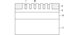
- 2 is an enlarged view of the area indicated by the dashed line in FIG. 1, including the active region and the termination region; This is a cross-sectional view corresponding to the a-a' cross section in Figure 2.
- 4 is a flowchart showing an example of a manufacturing method of a semiconductor device according to the embodiment.
- 1A to 1C are cross-sectional views showing an example of a manufacturing method of a semiconductor device in an embodiment.
- 1A to 1C are cross-sectional views showing an example of a manufacturing method of a semiconductor device in an embodiment.
- 1A to 1C are cross-sectional views showing an example of a manufacturing method of a semiconductor device in an embodiment.
- 1A to 1C are cross-sectional views showing an example of a manufacturing method of a semiconductor device in an embodiment.
- 2 is a cross-sectional view of a termination region of a semiconductor device according to an embodiment;
- 2 is a cross-sectional view of a termination region of a semiconductor device according to an embodiment;
- 1 is a plan view of a semiconductor device according to an embodiment;
- 18 is an enlarged view of the area indicated by the dashed dotted line in FIG. 17, including the active region and the termination region.
- 1 is a diagram conceptually illustrating an example of a configuration of a power conversion system including a power conversion device according to an embodiment.
- the upper surface of " or “the lower surface of " when it is stated that “the upper surface of " or “the lower surface of " is used, it is intended to include not only the upper surface or lower surface of the target component itself, but also a state in which another component is formed on the upper surface or lower surface of the target component.
- the upper surface of " or “the lower surface of " when it is stated that "B is provided on the upper surface of A,” it does not prevent another component "C" from being interposed between A and B.
- a power semiconductor device which is a MOSFET made of an n-channel SiC substrate.
- the semiconductor device is a planar gate type semiconductor device and includes a built-in Schottky barrier diode (SBD).
- FIG. 1 is a plan view of a semiconductor device according to this embodiment.
- a source electrode 3 is formed in the center of the top surface of the semiconductor device 1, and a gate wiring 2 is formed to surround the source electrode 3.
- a gate pad 4 is formed in the lower center and is electrically connected to the gate wiring 2.
- the region in which the unit cells are periodically arranged is defined as the active region, and the region other than the active region (the region surrounding the active region) is defined as the termination region.
- FIG. 2 is an enlarged view of the region including the active region and termination region indicated by the dashed line in FIG. 1.
- unit cells 14 (corresponding to the MOSFET region) are formed in a stripe pattern in active region 13, which is made up of a MOSFET region in which a MOSFET structure is formed and an SBD region in which an SBD structure is formed.
- FIG. 3 is a cross-sectional view corresponding to the a-a' cross section in FIG. 2.
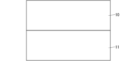
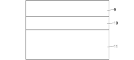
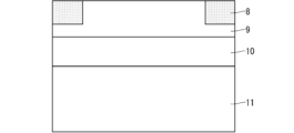
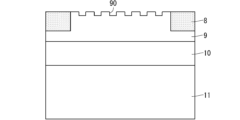
- the termination region of the semiconductor device includes an n-type SiC substrate 11, an n-type epitaxial growth layer 10 uniformly formed on the upper surface of the SiC substrate 11, an n-type n-well region 9 formed on the surface of the epitaxial growth layer 10, a p-type semiconductor region 7 partially formed on the surface of the n-well region 9, a p-type p-well region 8 partially formed on the surface of the n-well region 9, an interlayer insulating film 5 formed to cover a part of the upper surface of the p-well region 8, a barrier metal layer 6 formed to cover the interlayer insulating film 5, the n-well region 9, the p-type semiconductor region 7, and the p-well region 8, a source electrode 3 formed to cover the barrier metal layer 6, and a drain electrode 12 formed on the lower surface of the n-type SiC substrate 11.
- the interface between the p-type semiconductor region 7 and the barrier metal layer 6 is formed at a deeper position than the interface between the n-well region 9 and the barrier metal layer 6.
- the interface between the barrier metal layer 6 and the p-type semiconductor region 7, and part of the interface between the barrier metal layer 6 and the p-well region 8, are ohmic-connected.
- the interface between the barrier metal layer 6 and the n-well region 9 is Schottky-connected (i.e., the source electrode 3 and the n-well region 9 are Schottky-connected).
- the interface between the p-type semiconductor region 7 and the source electrode 3 (in FIG. 3, the interface between the p-type semiconductor region 7 and the barrier metal layer 6) is formed so as to satisfy D1>0, D2>0, and (D2 ⁇ 2)>D1.
- FIG. 4 is a flow chart showing an example of a method for manufacturing a semiconductor device according to the present embodiment.
- Fig. 5 to Fig. 14 are cross-sectional views showing an example of a method for manufacturing a semiconductor device according to the present embodiment.
- an epitaxial growth layer 10 made of n-type SiC is formed on the top surface (first main surface) of an n-type SiC substrate 11 having a polytype of 4H, for example, by chemical vapor deposition (CVD) (step ST1 in FIG. 4).
- CVD chemical vapor deposition
- impurities are ion-implanted into the surface layer of the epitaxial growth layer 10 to form an n-well region 9 (step ST2 in FIG. 4).
- the impurity concentration of the n-well region 9 is controlled to be higher than the impurity concentration of the epitaxial growth layer 10.
- an implantation mask is formed in a portion of the n-well region 9 using photoresist or the like (not shown here), and then p-type impurities are ion-implanted from the top surface of the n-well region 9 to form the p-well region 8 (step ST3 in FIG. 4).
- p-type impurities include B (boron) and Al (aluminum).
- the implantation depth of the p-well region 8 is controlled so as not to deviate from the n-well region 9 (i.e., so that the implantation depth of the p-well region 8 is not deeper than the bottom surface of the n-well region 9).
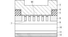
- an implantation mask is formed (not shown) using photoresist or the like in a portion of the n-well region 9 (in FIG. 8, the region where the p-well region 8 is not formed), and then a portion of the upper surface of the n-well region 9 is processed using dry etching or wet etching technology to form a recess 90 (step ST4 in FIG. 4).
- p-type impurities are ion-implanted into the recess 90 to form the p-type semiconductor region 7 (step ST5 in FIG. 4).
- the impurity concentration of the p-type semiconductor region 7 is controlled to be higher than the impurity concentration of the p-well region 8.
- the SiC substrate 11 is heat-treated at high temperature using a heat treatment device (not shown), and the implanted ions are electrically activated.
- an interlayer insulating film 5 is formed by a deposition method such as thermal oxidation or chemical vapor deposition, and then patterned using photolithography, dry etching, or wet etching so that the interlayer insulating film 5 remains in a predetermined area (step ST6 in FIG. 4).
- the interlayer insulating film may have a laminated structure of two or more layers of different materials.
- a barrier metal layer 6 is formed using a barrier metal made of titanium or a titanium compound such as titanium nitride (TiN).
- a film of aluminum, an aluminum alloy made of aluminum and silicon, or nickel is deposited to form the source electrode 3 (step ST7 in FIG. 4).
- a nickel film of about 600 nm is formed on the lower surface (second main surface) of the SiC substrate 11 by appropriately using a sputtering method or the like to form the drain electrode 12 (step ST9 in FIG. 4).
- the drain electrode 12 may be a laminated film made of a nickel film and gold or silver, etc., with a metal that is poorly reactive with the outside, such as gold (Au) or silver (Ag), used as a protective film on the nickel surface.
- This stress can cause the barrier metal layer 6 to peel off from the SiC substrate 11, or the source electrode 3 to peel off from the barrier metal layer 6.
- the amount of heat generated in the termination region increases compared to a semiconductor device without an SBD region. Therefore, when the barrier metal layer 6 and the source electrode 3 are formed on the top surface of the flat SiC substrate 11, there is a problem that the barrier metal layer 6 or the source electrode 3 peels off due to thermal stress caused by a rise in temperature when current is applied to the semiconductor device, as they have poor adhesion to lateral stress.
- the interface can be mechanically bonded (also called the anchor effect, fastener effect, or anchor effect) to increase adhesion and suppress peeling. This improves the reliability of the semiconductor device during operation.
- the p-type semiconductor region 7 by forming the p-type semiconductor region 7 by ion implanting p-type impurities into the recesses 90 of the n-well region 9, the p-type semiconductor region 7 can be formed to the same depth with lower acceleration energy compared to a structure in which ions are implanted without forming an uneven surface at the interface, and energy costs during manufacturing can be reduced. Furthermore, lowering the injection energy can reduce damage caused by ion implantation on the top surface of the SiC substrate 11, and suppress leakage current due to defects that may be formed due to the damage. This suppresses heat generation during operation of the semiconductor device 1, improving the reliability of the semiconductor device 1.
- Second Embodiment A semiconductor device and a method for manufacturing the semiconductor device according to the present embodiment will be described.
- components similar to those described in the above embodiment are illustrated with the same reference numerals, and detailed description thereof will be omitted as appropriate.
- the power semiconductor device according to the first embodiment is applied to a power conversion device.
- a power semiconductor device will be described using an n-channel MOSFET made of a SiC substrate.
- This semiconductor device is a planar gate type semiconductor device and has a built-in Schottky barrier diode (SBD).
- SBD Schottky barrier diode
- Figure 15 is a cross-sectional view of the termination region of the semiconductor device according to this embodiment.
- the device includes an n-type SiC substrate 11, an n-type epitaxial growth layer 10, an n-type n-well region 9, a plurality of p-type semiconductor regions 7a partially formed on the surface layer of the n-well region 9, a p-type p-well region 8, an interlayer insulating film 5, a barrier metal layer 6, a source electrode 3, and a drain electrode 12.
- a recess 90 is formed in the upper surface of the n-well region 9, as in the first embodiment.
- the p-type semiconductor region 7a is formed with a width that covers the recess 90 in a plan view (a range wider than the range in which the recess 90 is formed).
- the manufacturing method of the semiconductor device according to this embodiment differs in that, when ion-implanting p-type impurities to form p-type semiconductor region 7a, ion implantation is performed from a direction at an angle of 1° or more and 45° or less from a direction perpendicular to SiC substrate 11.
- the other manufacturing steps are the same as those shown in FIGS.
- the power semiconductor device according to the first or second embodiment is applied to a power conversion device.
- a power semiconductor device will be described, taking as an example a MOSFET made of an n-channel SiC substrate.
- This semiconductor device is a planar gate type semiconductor device, and includes a built-in Schottky barrier diode (SBD).
- SBD Schottky barrier diode
- Figure 16 is a cross-sectional view of the termination region of the semiconductor device according to this embodiment.
- the device includes an n-type SiC substrate 11, an n-type epitaxial growth layer 10, an n-type n-well region 9, a p-type semiconductor region 7, a p-type p-well region 8, an interlayer insulating film 5, a barrier metal layer 6b formed to cover the interlayer insulating film 5, the n-well region 9, the p-type semiconductor region 7, and the p-well region 8, a source electrode 3, and a drain electrode 12.
- a recess 90b is formed on the top surface of the n-well region 9.
- the interior angle of the bottom of the recess 90b is an obtuse angle of 90° or more.
- the barrier metal layer 6b is formed with an inclined surface so as to follow the shape of the recess 90b.
- the p-type semiconductor region provided below the recess 90b may be formed in an area larger than the area in which the recess 90b is formed.
- the manufacturing method of the semiconductor device according to this embodiment differs from the process of the first embodiment shown in Fig. 8 in that when forming the recess 90b, the side surface of the recess 90b is formed to be an inclined surface by wet etching or the like.
- the other manufacturing steps are the same as those shown in Figs. 5 to 14.
- a SiC semiconductor device that can suppress damage or peeling at the corners of the end of the recess 90 in a planar view by alleviating the concentration of electric field and stress at the corners of the end of the recess 90 in a planar view.
- FIG. 17 is an enlarged view of a region including the active region and the termination region of the above-mentioned SiC semiconductor device.
- FIG. 18 is an enlarged view of a region including a recess 90, which is indicated by a dashed line in FIG. 17.
- the concentration of electric fields and stresses at the corners of the end of the recess 90 in a planar view can be alleviated, thereby suppressing damage or peeling at the corners of the end of the recess 90 in a planar view.
- the mask for forming the recess 90 in step ST4 is changed. Then, through steps similar to steps ST5 to ST9 in the first embodiment, a SiC semiconductor device having a structure as shown in FIGS. 17 and 18 is formed.
- the semiconductor device according to the above-described embodiment is applied to a power converter.
- the power converter to which the semiconductor device is applied is not limited to a specific application, but the following describes a case where the semiconductor device is applied to a three-phase inverter.
- FIG. 19 is a conceptual diagram illustrating an example of the configuration of a power conversion system including the power conversion device of this embodiment.
- the power conversion device 2200 is a three-phase inverter connected between the power source 2100 and the load 2300.
- the power conversion device 2200 converts the DC power supplied from the power source 2100 into AC power, and further supplies the AC power to the load 2300.
- the power conversion device 2200 includes a conversion circuit 2201 that converts DC power into AC power and outputs it, a drive circuit 2202 that outputs drive signals for driving each switching element of the conversion circuit 2201, and a control circuit 2203 that outputs a control signal to the drive circuit 2202 to control the drive circuit 2202.
- the conversion circuit 2201 in this embodiment is a two-level three-phase full bridge circuit, and has six switching elements and six freewheeling diodes connected in anti-parallel to each switching element.
- a semiconductor device is applied to at least one of the switching elements and free wheel diodes in the conversion circuit 2201.
- the six switching elements are connected in series in groups of two to form upper and lower arms, and each upper and lower arm forms one phase of the full bridge circuit (i.e., U phase, V phase, and W phase).
- the output terminals of each upper and lower arm i.e., the three output terminals of the conversion circuit 2201 are connected to the load 2300.
- the drive circuit 2202 generates a drive signal for driving the switching element of the conversion circuit 2201, and further supplies the drive signal to the control electrode of the switching element of the conversion circuit 2201. Specifically, based on a control signal output from the control circuit 2203 described below, the drive circuit 2202 outputs a drive signal for turning the switching element on and a drive signal for turning the switching element off to the control electrodes of the respective switching elements.
- the drive signal When the switching element is maintained in the on state, the drive signal is a voltage signal equal to or greater than the threshold voltage of the switching element (i.e., an on signal), and when the switching element is maintained in the off state, the drive signal is a voltage signal equal to or less than the threshold voltage of the switching element (i.e., an off signal).
- the semiconductor device in any of the embodiments described above may be applied to a three-level or multi-level power conversion device.
- the semiconductor device in any of the embodiments described above may be applied to a single-phase inverter.
- the semiconductor device when supplying power to a DC load, can be applied to a DC-DC converter or an AC-DC converter.
- a power conversion device to which a semiconductor device according to any of the above-described embodiments is applied is not limited to cases in which the load described above is an electric motor, and can also be used, for example, as a power supply device for an electric discharge machine, a laser processing machine, an induction heating cooker, or a non-contact power supply system.Furthermore, a power conversion device to which a semiconductor device according to any of the above-described embodiments is applied can also be used as a power conditioner in a solar power generation system or a power storage system, etc.
- a semiconductor device is manufactured using the manufacturing method described in the embodiment described above. Then, a conversion circuit 2201 having the semiconductor device is provided as a component of a power conversion device.
- the conversion circuit 2201 is a circuit for converting input power and outputting it.
- a drive circuit 2202 is provided as a component of the power conversion device.
- the drive circuit 2202 is a circuit for outputting a drive signal to the semiconductor device for driving the semiconductor device.
- the power conversion device is further provided with a control circuit 2203.
- the control circuit 2203 is a circuit for outputting a control signal to the drive circuit 2202 for controlling the drive circuit 2202.
- the semiconductor switching elements used in the embodiments described above are not limited to switching elements made of silicon (Si) semiconductors, and may be made of, for example, non-Si semiconductor materials that have a wider band gap than Si semiconductors.
- Wide band gap semiconductors that are non-Si semiconductor materials include, for example, silicon carbide, gallium nitride-based materials, and diamond.
- Switching elements made of wide bandgap semiconductors can be used in high voltage regions where unipolar operation is difficult with silicon semiconductors, and can significantly reduce the switching losses that occur during switching operations. This allows for a significant reduction in power loss.
- switching elements made of wide band gap semiconductors have low power loss and high heat resistance. Therefore, when configuring a power module with a cooling section, it is possible to reduce the size of the heat dissipation fins of the heat sink, making it possible to further reduce the size of the semiconductor module.
- switching elements made of wide bandgap semiconductors are suitable for high-frequency switching operations. Therefore, when applied to converter circuits that require high frequencies, increasing the switching frequency can also reduce the size of reactors or capacitors connected to the converter circuit.
- the semiconductor switching element in the above-described embodiment is a switching element made of a wide-gap semiconductor such as silicon carbide.
- the semiconductor device includes an active region 13 and a termination region surrounding the active region 13 in a planar view.
- the termination region includes a first semiconductor layer of a first conductivity type (n-type), a second semiconductor layer of a second conductivity type (p-type), and a top electrode.
- the first semiconductor layer corresponds to, for example, the n-well region 9.
- the second semiconductor layer corresponds to, for example, at least one of the p-type semiconductor region 7, the p-type semiconductor region 7a, and the p-well region 8.
- the top electrode corresponds to, for example, the source electrode 3. At least one p-type semiconductor region 7 is provided on the surface layer of the n-well region 9.
- the source electrode 3 covers the n-well region 9 and the p-type semiconductor region 7.
- the source electrode 3 is connected to the n-well region 9 via a Schottky connection.
- at least one interface between the p-type semiconductor region 7 and the source electrode 3 (if a barrier metal layer 6 is present, the interface between the barrier metal layer 6 and the p-type semiconductor region 7) is located deeper than the interface between the n-well region 9 and the source electrode 3 (if a barrier metal layer 6 is present, the interface between the barrier metal layer 6 and the n-well region 9).
- the interface between the p-type semiconductor region 7 and the source electrode 3 is located deeper than the interface between the n-well region 9 and the source electrode 3, and the mechanical bond at this location improves adhesion, making it possible to suppress peeling of the source electrode 3 from the barrier metal layer 6 or the n-well region 9 due to thermal stress caused by a rise in temperature of the semiconductor device. This improves the reliability of the semiconductor device during operation.
- the distance from the interface between the n-well region 9 and the source electrode 3 (if a barrier metal layer 6 is present, the interface between the barrier metal layer 6 and the n-well region 9) to the interface between the p-type semiconductor region 7 and the source electrode 3 (if a barrier metal layer 6 is present, the interface between the barrier metal layer 6 and the p-type semiconductor region 7) is D1
- the distance from the interface between the n-well region 9 and the source electrode 3 (if a barrier metal layer 6 is present, the interface between the barrier metal layer 6 and the n-well region 9) to the underside of the p-type semiconductor region 7 is D2
- the interface between the p-type semiconductor region 7 and the source electrode 3 (if a barrier metal layer 6 is present, the interface between the barrier metal layer 6 and the p-type semiconductor region 7) is formed so as to satisfy D1>0, D2>0, and (D2 ⁇ 2)>D1.
- This configuration makes it possible to suppress peeling between the source electrode 3 and the n-well region 9 (or between the source electrode 3 and the barrier metal layer 6, or between the barrier metal layer 6 and the n-well region 9, if a barrier metal layer 6 is used) due to thermal stress that occurs during operation of the semiconductor device, without impairing the characteristics of the JBS.
- the active region 13 has a Schottky barrier diode structure.
- the active region 13 has a MOSFET structure.
- the region having the MOSFET structure and the region having the Schottky barrier diode structure are periodically arranged in a striped pattern in a plan view.
- a recess 90 (or recess 90b) is formed on the upper surface of the n-well region 9.
- the p-type semiconductor region 7a is provided to cover an area larger than the area in which the recess 90 (or recess 90b) is formed.
- the side surface of the recess 90b is an inclined surface.
- the power conversion device has the above-mentioned semiconductor device, and is equipped with a conversion circuit 2201 that converts and outputs input power, a drive circuit 2202 that outputs a drive signal to the semiconductor device for driving the semiconductor device, and a control circuit 2203 that outputs a control signal to the drive circuit 2202 for controlling the drive circuit 2202.
- the interface between the p-type semiconductor region 7 and the source electrode 3 is located deeper than the interface between the n-well region 9 and the source electrode 3, and the adhesion is improved by mechanical bonding at that location, so that peeling of the source electrode 3 from the barrier metal layer 6 or the n-well region 9 can be suppressed due to thermal stress caused by a temperature rise in the semiconductor device. This can improve the reliability of the semiconductor device during operation.
- At least one p-type semiconductor region 7 of a second conductivity type is provided on the surface of an n-well region 9 of a first conductivity type in the termination region.
- a source electrode 3 is provided in the termination region to cover the n-well region 9 and the p-type semiconductor region 7.
- the source electrode 3 is connected to the n-well region 9 by a Schottky connection.
- at least one interface between the p-type semiconductor region 7 and the source electrode 3 is located deeper than the interface between the n-well region 9 and the source electrode 3.
- the interface between the p-type semiconductor region 7 and the source electrode 3 is located deeper than the interface between the n-well region 9 and the source electrode 3, and the mechanical bond at this location improves adhesion, making it possible to suppress peeling of the source electrode 3 from the barrier metal layer 6 or the n-well region 9 due to thermal stress caused by a rise in temperature of the semiconductor device. This improves the reliability of the semiconductor device during operation.
- a conversion circuit 2201 that has a semiconductor device manufactured by the above manufacturing method and converts and outputs input power.
- a drive circuit 2202 is provided that outputs a drive signal to the semiconductor device for driving the semiconductor device.
- a control circuit 2203 is provided that outputs a control signal to the drive circuit 2202 for controlling the drive circuit 2202.
- the interface between the p-type semiconductor region 7 and the source electrode 3 is located deeper than the interface between the n-well region 9 and the source electrode 3, and the adhesion is improved by mechanical bonding at that location, so that peeling of the source electrode 3 from the barrier metal layer 6 or the n-well region 9 can be suppressed due to thermal stress caused by a rise in temperature of the semiconductor device. This can improve the reliability of the semiconductor device during operation.
- each component in the embodiments described above is a conceptual unit, and the scope of the technology disclosed in this specification includes cases where one component is made up of multiple structures, where one component corresponds to a part of a structure, and even where multiple components are provided in one structure.
- each component in the embodiments described above includes structures having other structures or shapes as long as they perform the same function.
- (Appendix 1) an active region and a termination region surrounding the active region in a plan view; In the termination region, a first semiconductor layer of a first conductivity type; At least one second semiconductor layer of a second conductivity type is provided on a surface layer of the first semiconductor layer; a top electrode covering the first semiconductor layer and the second semiconductor layer; the upper electrode is in Schottky contact with the first semiconductor layer; At least one interface between the second semiconductor layer and the top electrode is located deeper than an interface between the first semiconductor layer and the top electrode.
- Semiconductor device In the termination region, a first semiconductor layer of a first conductivity type; At least one second semiconductor layer of a second conductivity type is provided on a surface layer of the first semiconductor layer; a top electrode covering the first semiconductor layer and the second semiconductor layer; the upper electrode is in Schottky contact with the first semiconductor layer; At least one interface between the second semiconductor layer and the top electrode is located deeper than an interface between the first semiconductor layer and the top electrode.
- (Appendix 2) 2. The semiconductor device according to claim 1, a distance from an interface between the first semiconductor layer and the upper electrode to an interface between the second semiconductor layer and the upper electrode is defined as D1; When the distance from the interface between the first semiconductor layer and the upper electrode to the lower surface of the second semiconductor layer is D2, The interface between the second semiconductor layer and the upper electrode is formed so as to satisfy D1>0, D2>0, and (D2 ⁇ 2)>D1. Semiconductor device.
- the semiconductor device according to claim 1 The active region has a Schottky barrier diode structure.
- the semiconductor device according to claim 3 has a MOSFET structure, a region having a MOSFET structure and a region having a Schottky barrier diode structure are periodically arranged in a striped pattern in a plan view; Semiconductor device.
- a semiconductor device according to any one of claims 1 to 4, A recess is formed on an upper surface of the first semiconductor layer, The second semiconductor layer is provided to cover an area larger than an area in which the recess is formed. Semiconductor device.
- At least one corner of the end of the second semiconductor layer in a plan view is an obtuse angle or a curved surface.
- a conversion circuit including the semiconductor device according to any one of claims 1 to 7 and configured to convert and output an input power; a drive circuit that outputs a drive signal for driving the semiconductor device to the semiconductor device; a control circuit that outputs a control signal to the drive circuit for controlling the drive circuit; Power conversion equipment.
- a method for manufacturing a semiconductor device including an active region and a termination region surrounding the active region in a plan view, In the termination region, At least one second semiconductor layer of a second conductivity type is provided on a surface layer of a first semiconductor layer of a first conductivity type; providing a top electrode covering the first semiconductor layer and the second semiconductor layer; the upper electrode is in Schottky contact with the first semiconductor layer; At least one interface between the second semiconductor layer and the top electrode is located deeper than an interface between the first semiconductor layer and the top electrode.
- 1 semiconductor device 2 gate wiring, 3 source electrode, 4 gate pad, 5 interlayer insulating film, 6 barrier metal layer, 6b barrier metal layer, 7 p-type semiconductor region, 7a p-type semiconductor region, 8 p-well region, 9 n-well region, 10 epitaxial growth layer, 11 SiC substrate, 12 drain electrode, 13 active region, 14 unit cell, 90 recess, 90b recess, 2100 power supply, 2200 power conversion device, 2201 conversion circuit, 2202 drive circuit, 2203 control circuit, 2300 load.
Landscapes
- Electrodes Of Semiconductors (AREA)
Priority Applications (1)
| Application Number | Priority Date | Filing Date | Title |
|---|---|---|---|
| JP2025527838A JPWO2024257633A1 (https=) | 2023-06-16 | 2024-06-03 |
Applications Claiming Priority (2)
| Application Number | Priority Date | Filing Date | Title |
|---|---|---|---|
| JP2023098969 | 2023-06-16 | ||
| JP2023-098969 | 2023-06-16 |
Publications (1)
| Publication Number | Publication Date |
|---|---|
| WO2024257633A1 true WO2024257633A1 (ja) | 2024-12-19 |
Family
ID=93851887
Family Applications (1)
| Application Number | Title | Priority Date | Filing Date |
|---|---|---|---|
| PCT/JP2024/020150 Ceased WO2024257633A1 (ja) | 2023-06-16 | 2024-06-03 | 半導体装置、電力変換装置、半導体装置の製造方法 |
Country Status (2)
| Country | Link |
|---|---|
| JP (1) | JPWO2024257633A1 (https=) |
| WO (1) | WO2024257633A1 (https=) |
Citations (4)
| Publication number | Priority date | Publication date | Assignee | Title |
|---|---|---|---|---|
| WO2014038225A1 (ja) * | 2012-09-06 | 2014-03-13 | 三菱電機株式会社 | 炭化珪素半導体装置およびその製造方法 |
| WO2014155651A1 (ja) * | 2013-03-29 | 2014-10-02 | 株式会社日立製作所 | 炭化珪素半導体装置及びその製造方法 |
| WO2016052261A1 (ja) * | 2014-10-01 | 2016-04-07 | 三菱電機株式会社 | 半導体装置 |
| WO2019124378A1 (ja) * | 2017-12-19 | 2019-06-27 | 三菱電機株式会社 | 炭化珪素半導体装置および電力変換装置 |
-
2024
- 2024-06-03 JP JP2025527838A patent/JPWO2024257633A1/ja active Pending
- 2024-06-03 WO PCT/JP2024/020150 patent/WO2024257633A1/ja not_active Ceased
Patent Citations (4)
| Publication number | Priority date | Publication date | Assignee | Title |
|---|---|---|---|---|
| WO2014038225A1 (ja) * | 2012-09-06 | 2014-03-13 | 三菱電機株式会社 | 炭化珪素半導体装置およびその製造方法 |
| WO2014155651A1 (ja) * | 2013-03-29 | 2014-10-02 | 株式会社日立製作所 | 炭化珪素半導体装置及びその製造方法 |
| WO2016052261A1 (ja) * | 2014-10-01 | 2016-04-07 | 三菱電機株式会社 | 半導体装置 |
| WO2019124378A1 (ja) * | 2017-12-19 | 2019-06-27 | 三菱電機株式会社 | 炭化珪素半導体装置および電力変換装置 |
Also Published As
| Publication number | Publication date |
|---|---|
| JPWO2024257633A1 (https=) | 2024-12-19 |
Similar Documents
| Publication | Publication Date | Title |
|---|---|---|
| US11984492B2 (en) | Silicon carbide semiconductor device, power converter, and method of manufacturing silicon carbide semiconductor device | |
| JP6870119B2 (ja) | 半導体装置および電力変換装置 | |
| US20190057873A1 (en) | Semiconductor device, method of manufacturing same, and power converter | |
| JP6514338B2 (ja) | 半導体装置、パワーモジュール、電力変換装置、自動車および鉄道車両 | |
| JPWO2018155566A1 (ja) | 炭化珪素半導体装置および電力変換装置 | |
| US11915988B2 (en) | Semiconductor device and power converter | |
| JP6652802B2 (ja) | 半導体装置、および当該半導体装置を備えるインバータ装置 | |
| JPWO2020026401A1 (ja) | ワイドバンドギャップ半導体装置、および、電力変換装置 | |
| JP7094439B2 (ja) | 炭化珪素半導体装置および電力変換装置 | |
| JP7778041B2 (ja) | 半導体装置および電力変換装置 | |
| CN116325176B (zh) | 碳化硅半导体装置以及电力变换装置 | |
| JP7047981B1 (ja) | 炭化珪素半導体装置および電力変換装置 | |
| CN115668510A (zh) | 碳化硅半导体装置以及电力变换装置 | |
| JP6873273B2 (ja) | 炭化珪素半導体装置および電力変換装置 | |
| WO2019176466A1 (ja) | 半導体装置、電力変換装置 | |
| JP2019091754A (ja) | 炭化ケイ素半導体装置、電力変換装置および炭化ケイ素半導体装置の製造方法 | |
| WO2024257633A1 (ja) | 半導体装置、電力変換装置、半導体装置の製造方法 | |
| JP7262672B2 (ja) | 半導体装置および電力変換装置 | |
| US11296191B2 (en) | Power module and power converter | |
| US12464767B2 (en) | Semiconductor device and power conversion device | |
| CN116207140A (zh) | 半导体装置及电力变换装置 | |
| JP2024097559A (ja) | 半導体装置、電力変換装置および半導体装置の製造方法 | |
| WO2024237071A1 (ja) | 半導体装置、電力変換装置、半導体装置の製造方法、および、電力変換装置の製造方法 | |
| WO2025225432A1 (ja) | 半導体装置、および、電力変換装置 | |
| JP7607834B1 (ja) | 半導体装置、半導体装置の製造方法、及び、電力変換装置 |
Legal Events
| Date | Code | Title | Description |
|---|---|---|---|
| 121 | Ep: the epo has been informed by wipo that ep was designated in this application |
Ref document number: 24823253 Country of ref document: EP Kind code of ref document: A1 |
|
| WWE | Wipo information: entry into national phase |
Ref document number: 2025527838 Country of ref document: JP |
|
| NENP | Non-entry into the national phase |
Ref country code: DE |