WO2024252950A1 - 接着フィルムの製造方法及び接着フィルム、並びに、構造体の製造方法及び構造体 - Google Patents
接着フィルムの製造方法及び接着フィルム、並びに、構造体の製造方法及び構造体 Download PDFInfo
- Publication number
- WO2024252950A1 WO2024252950A1 PCT/JP2024/019117 JP2024019117W WO2024252950A1 WO 2024252950 A1 WO2024252950 A1 WO 2024252950A1 JP 2024019117 W JP2024019117 W JP 2024019117W WO 2024252950 A1 WO2024252950 A1 WO 2024252950A1
- Authority
- WO
- WIPO (PCT)
- Prior art keywords
- curing agent
- film
- film layer
- latent curing
- latent
- Prior art date
- Legal status (The legal status is an assumption and is not a legal conclusion. Google has not performed a legal analysis and makes no representation as to the accuracy of the status listed.)
- Ceased
Links
Images


Classifications
-
- C—CHEMISTRY; METALLURGY
- C08—ORGANIC MACROMOLECULAR COMPOUNDS; THEIR PREPARATION OR CHEMICAL WORKING-UP; COMPOSITIONS BASED THEREON
- C08G—MACROMOLECULAR COMPOUNDS OBTAINED OTHERWISE THAN BY REACTIONS ONLY INVOLVING UNSATURATED CARBON-TO-CARBON BONDS
- C08G59/00—Polycondensates containing more than one epoxy group per molecule; Macromolecules obtained by polymerising compounds containing more than one epoxy group per molecule using curing agents or catalysts which react with the epoxy groups
- C08G59/18—Macromolecules obtained by polymerising compounds containing more than one epoxy group per molecule using curing agents or catalysts which react with the epoxy groups ; e.g. general methods of curing
- C08G59/68—Macromolecules obtained by polymerising compounds containing more than one epoxy group per molecule using curing agents or catalysts which react with the epoxy groups ; e.g. general methods of curing characterised by the catalysts used
- C08G59/70—Chelates
-
- C—CHEMISTRY; METALLURGY
- C08—ORGANIC MACROMOLECULAR COMPOUNDS; THEIR PREPARATION OR CHEMICAL WORKING-UP; COMPOSITIONS BASED THEREON
- C08L—COMPOSITIONS OF MACROMOLECULAR COMPOUNDS
- C08L63/00—Compositions of epoxy resins; Compositions of derivatives of epoxy resins
-
- C—CHEMISTRY; METALLURGY
- C08—ORGANIC MACROMOLECULAR COMPOUNDS; THEIR PREPARATION OR CHEMICAL WORKING-UP; COMPOSITIONS BASED THEREON
- C08L—COMPOSITIONS OF MACROMOLECULAR COMPOUNDS
- C08L71/00—Compositions of polyethers obtained by reactions forming an ether link in the main chain; Compositions of derivatives of such polymers
-
- C—CHEMISTRY; METALLURGY
- C09—DYES; PAINTS; POLISHES; NATURAL RESINS; ADHESIVES; COMPOSITIONS NOT OTHERWISE PROVIDED FOR; APPLICATIONS OF MATERIALS NOT OTHERWISE PROVIDED FOR
- C09J—ADHESIVES; NON-MECHANICAL ASPECTS OF ADHESIVE PROCESSES IN GENERAL; ADHESIVE PROCESSES NOT PROVIDED FOR ELSEWHERE; USE OF MATERIALS AS ADHESIVES
- C09J11/00—Features of adhesives not provided for in group C09J9/00, e.g. additives
- C09J11/02—Non-macromolecular additives
- C09J11/06—Non-macromolecular additives organic
-
- C—CHEMISTRY; METALLURGY
- C09—DYES; PAINTS; POLISHES; NATURAL RESINS; ADHESIVES; COMPOSITIONS NOT OTHERWISE PROVIDED FOR; APPLICATIONS OF MATERIALS NOT OTHERWISE PROVIDED FOR
- C09J—ADHESIVES; NON-MECHANICAL ASPECTS OF ADHESIVE PROCESSES IN GENERAL; ADHESIVE PROCESSES NOT PROVIDED FOR ELSEWHERE; USE OF MATERIALS AS ADHESIVES
- C09J163/00—Adhesives based on epoxy resins; Adhesives based on derivatives of epoxy resins
-
- C—CHEMISTRY; METALLURGY
- C09—DYES; PAINTS; POLISHES; NATURAL RESINS; ADHESIVES; COMPOSITIONS NOT OTHERWISE PROVIDED FOR; APPLICATIONS OF MATERIALS NOT OTHERWISE PROVIDED FOR
- C09J—ADHESIVES; NON-MECHANICAL ASPECTS OF ADHESIVE PROCESSES IN GENERAL; ADHESIVE PROCESSES NOT PROVIDED FOR ELSEWHERE; USE OF MATERIALS AS ADHESIVES
- C09J171/00—Adhesives based on polyethers obtained by reactions forming an ether link in the main chain; Adhesives based on derivatives of such polymers
-
- C—CHEMISTRY; METALLURGY
- C09—DYES; PAINTS; POLISHES; NATURAL RESINS; ADHESIVES; COMPOSITIONS NOT OTHERWISE PROVIDED FOR; APPLICATIONS OF MATERIALS NOT OTHERWISE PROVIDED FOR
- C09J—ADHESIVES; NON-MECHANICAL ASPECTS OF ADHESIVE PROCESSES IN GENERAL; ADHESIVE PROCESSES NOT PROVIDED FOR ELSEWHERE; USE OF MATERIALS AS ADHESIVES
- C09J201/00—Adhesives based on unspecified macromolecular compounds
-
- C—CHEMISTRY; METALLURGY
- C09—DYES; PAINTS; POLISHES; NATURAL RESINS; ADHESIVES; COMPOSITIONS NOT OTHERWISE PROVIDED FOR; APPLICATIONS OF MATERIALS NOT OTHERWISE PROVIDED FOR
- C09J—ADHESIVES; NON-MECHANICAL ASPECTS OF ADHESIVE PROCESSES IN GENERAL; ADHESIVE PROCESSES NOT PROVIDED FOR ELSEWHERE; USE OF MATERIALS AS ADHESIVES
- C09J7/00—Adhesives in the form of films or foils
- C09J7/30—Adhesives in the form of films or foils characterised by the adhesive composition
-
- C—CHEMISTRY; METALLURGY
- C09—DYES; PAINTS; POLISHES; NATURAL RESINS; ADHESIVES; COMPOSITIONS NOT OTHERWISE PROVIDED FOR; APPLICATIONS OF MATERIALS NOT OTHERWISE PROVIDED FOR
- C09J—ADHESIVES; NON-MECHANICAL ASPECTS OF ADHESIVE PROCESSES IN GENERAL; ADHESIVE PROCESSES NOT PROVIDED FOR ELSEWHERE; USE OF MATERIALS AS ADHESIVES
- C09J7/00—Adhesives in the form of films or foils
- C09J7/30—Adhesives in the form of films or foils characterised by the adhesive composition
- C09J7/35—Heat-activated
-
- C—CHEMISTRY; METALLURGY
- C09—DYES; PAINTS; POLISHES; NATURAL RESINS; ADHESIVES; COMPOSITIONS NOT OTHERWISE PROVIDED FOR; APPLICATIONS OF MATERIALS NOT OTHERWISE PROVIDED FOR
- C09J—ADHESIVES; NON-MECHANICAL ASPECTS OF ADHESIVE PROCESSES IN GENERAL; ADHESIVE PROCESSES NOT PROVIDED FOR ELSEWHERE; USE OF MATERIALS AS ADHESIVES
- C09J9/00—Adhesives characterised by their physical nature or the effects produced, e.g. glue sticks
- C09J9/02—Electrically-conducting adhesives
-
- H—ELECTRICITY
- H01—ELECTRIC ELEMENTS
- H01B—CABLES; CONDUCTORS; INSULATORS; SELECTION OF MATERIALS FOR THEIR CONDUCTIVE, INSULATING OR DIELECTRIC PROPERTIES
- H01B5/00—Non-insulated conductors or conductive bodies characterised by their form
- H01B5/14—Non-insulated conductors or conductive bodies characterised by their form comprising conductive layers or films on insulating-supports
Definitions
- This technology relates to a method for producing an adhesive film containing a curing agent, an adhesive film, and a method for producing a structure and a structure.
- the hardener used in adhesive films is a latent hardener that only becomes reactive when exposed to external stimuli such as heat or light.
- Patent Document 1 describes a technology that makes it possible to use a two-liquid adhesive that is used by mixing two liquids as a one-liquid type by encapsulating a hardener that can be used in low-temperature reactions and making it latent.
- This technology solves the problems mentioned above, and provides a method for producing an adhesive film with excellent storage stability, an adhesive film, a method for producing a structure, and a structure.
- the curing agent-free adhesive composition comprises a film-forming resin, a cationically polymerizable compound, and a silane-based compound;
- a latent curing agent is exposed from at least one surface or disposed adjacent to at least one surface, the film layer containing conductive particles;
- the average particle size of the latent curing agent is 2 ⁇ m or more and 50 ⁇ m or less, The conductive film, wherein the thickness of the film layer is 3 ⁇ m or more and 40 ⁇ m or less.
- a latent curing agent is exposed from at least one surface or disposed adjacent to at least one surface, the film layer containing conductive particles;
- the average particle size of the latent curing agent is 2 ⁇ m or more and 50 ⁇ m or less,
- the thickness of the film layer is 3 ⁇ m or more and 40 ⁇ m or less.
- [10] A method for manufacturing a structure in which a first component and a second component are bonded together via the adhesive film according to [7] above.
- [11] A method for manufacturing a connection structure that connects a terminal of a first component and a terminal of a second component via the adhesive film described in [7] above, the conductive film described in [8] above, or the anisotropic conductive film described in [9] above.
- [12] A structure in which a first part and a second part are bonded via the adhesive film according to [7] above.
- connection structure in which a terminal of a first electronic component and a terminal of a second electronic component are connected via the adhesive film described in [7] above, the conductive film described in [8] above, or the anisotropic conductive film described in [9] above.
- the latent hardener by disposing the latent hardener after film formation, the progress of the hardening reaction caused by the solvent of the latent hardener can be suppressed, and excellent storage stability can be obtained.
- the latent hardener by disposing the latent hardener on the surface of the film layer, the reaction caused by the hardener is initiated, and excellent adhesive strength can be obtained.
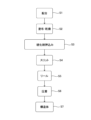
- FIG. 1 is a flow chart showing the process from production to use of an adhesive film according to the present embodiment.
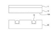
- FIG. 2 is a cross-sectional view that typically shows a state in which a transfer substrate filled with a latent curing agent and a film layer are placed opposite each other.
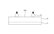
- FIG. 3 is a cross-sectional view that typically shows a state in which a latent curing agent is attached to the surface of a film layer.
- FIG. 4 is a cross-sectional view that shows a schematic state in which the latent curing agent is pressed into the film layer.
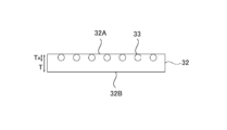
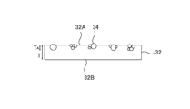
- FIG. 5 is a cross-sectional view that illustrates a schematic diagram of an adhesive film according to a first embodiment.
- FIG. 1 is a flow chart showing the process from production to use of an adhesive film according to the present embodiment.
- FIG. 2 is a cross-sectional view that typically shows a state in which a transfer substrate filled with a latent curing agent and a film layer are placed opposite each other.
- FIG. 3 is
- FIG. 6 is a cross-sectional view that illustrates a modified example of the adhesive film of the first embodiment.
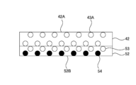
- FIG. 7 is a cross-sectional view that illustrates a schematic diagram of an adhesive film according to the second embodiment.
- FIG. 8 is a cross-sectional view that illustrates a schematic diagram of an adhesive film according to a third embodiment.
- the method for producing an adhesive film according to the present embodiment includes a forming step of forming a film layer of a curing agent-free adhesive composition that does not contain a curing agent, and a disposing step of transferring a latent curing agent from a transfer substrate on which the latent curing agent is disposed to the film layer, and exposing the latent curing agent from at least one surface of the film layer or disposing the latent curing agent in close proximity to at least one surface of the film layer.
- a hardener-free adhesive composition is one that does not contain a hardener and does not function as an adhesive when subjected to external stimuli such as heat or light.
- a latent hardener is one that becomes reactive only when subjected to external stimuli such as heat or light, and is in the form of powdered solid particles. Powdered solid particles are preferably capable of being observed under a microscope at 5 to 35°C.
- latent hardeners include microcapsule types in which the hardener component is used as a core and is covered with a coating agent (shell) such as an organic polymer or inorganic compound, and impregnated types in which the hardener component is encapsulated in porous particles.
- the manufacturing to use of the adhesive film includes a blending step S1 of blending a hardener-free adhesive composition, a coating and drying step S2 of applying and drying the hardener-free adhesive composition to obtain a film, a hardener pushing step S3 of pushing a hardener into the surface of the film, a slitting step S4 of obtaining a film of a predetermined width, a reeling step S5 of winding a film of a predetermined width, a pressure bonding step S6 of pulling out the film from the reel and pressure bonding a first electronic component and a second electronic component through the film, and a structure step S7 of obtaining a structure including the first electronic component and the second electronic component.
- the conductive particles when manufacturing an anisotropic conductive film in which conductive particles are arranged as an example of an adhesive film, it is preferable to arrange the conductive particles before or after the hardener pushing step S3.
- the conductive particles may be mixed in advance in the blending step S1, in which case the conductive particles are three-dimensionally and randomly dispersed in the adhesive film.
- the production of adhesive film begins by calculating backwards from the mixing time when the hardener is added to the bonding process in anticipation of the reaction of the hardener, so the production line must run continuously until the film is wound around the reel and shipped as a roll, which places constraints on production management.
- the roll is stored and managed under the constraints of the manufacturing management of the structure until the adhesive film is no longer in use (completion of the connection process).
- the hardener since the hardener is not added in the blending step S1, the restrictions on the amount and type of solvent can be reduced.
- the curing reaction can be prevented from progressing due to the heat of drying during film formation.
- the hardener pushing step S3 is the start of the reaction of the hardener, and since the manufacturing process (mass production line) can be temporarily stopped before the hardener pushing step S3, the life of the product can be easily controlled when calculated backwards from the pressure bonding step S6.
- the manufacturing schedule and time management become more flexible, there is an industrial advantage in that the constraints on manufacturing management are significantly reduced compared to the conventional method.
- the adhesive film may be a wound body wound on a reel, and the length of the adhesive film is preferably, for example, 5 m or more because it can be connected using an apparatus, and is preferably 5000 m or less in terms of attachment to the apparatus.
- the width of the adhesive film is preferably, for example, 0.5 mm or more and 60 cm or less.
- the adhesive film may also be in the form of a sheet, and there is no particular limit to its size, but it is preferable that one side is at least 5 cm, and more preferably at least 20 cm in terms of use. When it is in the form of a sheet, the maximum length of one side is preferably, for example, 200 cm or less for ease of handling.
- Figure 2 is a cross-sectional view that shows a state in which a transfer substrate filled with a latent hardener is opposed to a film layer
- Figure 3 is a cross-sectional view that shows a state in which a latent hardener is attached to the surface of the film layer
- Figure 4 is a cross-sectional view that shows a state in which the latent hardener has been pressed into the film layer.
- a curing agent-free adhesive composition that does not contain a curing agent is prepared.
- the adhesive composition can use a known insulating binder.
- the curing type can be a heat curing type, a light curing type, a light and heat combined curing type, etc., for example, a thermal cationic polymerization type resin composition containing an epoxy compound and a thermal cationic polymerization initiator, a thermal anionic polymerization type resin composition containing an epoxy compound and a thermal anionic polymerization initiator, a photoradical polymerization type resin composition containing a (meth)acrylate compound and a photoradical polymerization initiator, a thermal radical polymerization type resin composition containing a (meth)acrylate compound and a thermal radical polymerization initiator, etc. That is, in the case of a thermal cationic polymerization type resin composition, the curing agent-free adhesive composition does not contain a thermal cationic polymerization
- a solvent can be used to prepare the hardener-free adhesive composition.
- the solvent include propylene glycol monomethyl ether acetate (PMA) and methyl ethyl ketone (MEK).
- the hardener-free adhesive composition is applied onto the substrate film 11 and dried to evaporate the solvent, forming a film layer 12 of the hardener-free adhesive composition of a predetermined thickness on the substrate film 11.
- the amount of remaining solvent in the film layer 12 is preferably less than 1%, more preferably less than 0.5%, and even more preferably less than 0.1%. This makes it possible to suppress the progress of the hardening reaction caused by the solvent of the latent hardener, and to obtain excellent storage stability.
- a PET film that has been subjected to a release treatment using a silicone resin can be suitably used as the substrate film 11.
- the latent curing agent 13 is held on the first surface 12A of the film layer 12.
- methods for holding the latent curing agent 13 include a transfer method in which the latent curing agent 13 is transferred to the film layer 12 using a transfer substrate 20, and a spraying method in which the latent curing agent 13 is sprayed on the film layer 12.
- the transfer method can uniformly dispose the latent curing agent in a plan view, and can also uniformly dispose the latent curing agent in the thickness direction by pressing it with a flat plate or the like after transfer, thereby obtaining excellent adhesive strength (die shear strength, peel strength).
- a transfer substrate 20 filled with a latent hardener 13 is placed opposite a film layer 12, and the film layer 12 is pressed against the transfer substrate 20, so that the latent hardener 13 is held on the first surface 12A of the film layer 12.
- the transfer substrate 20 has recesses of a predetermined density formed in a predetermined arrangement.
- a transfer substrate 20 can be produced, for example, by creating a mold having protrusions of a predetermined density in a predetermined arrangement, pouring molten resin pellets into the mold, and cooling and solidifying them.
- the transfer substrate 20 may also be made of inorganic materials such as silicon, ceramics, glass, and metals such as stainless steel, or organic materials such as various resins, with openings formed by a known opening forming method such as photolithography.
- the transfer substrate 20 may be in the form of a plate or a roll.
- the latent hardener 13 attached to the first surface 12A of the film layer 12 is pressed into the film layer 12. This allows the latent hardener 13 to be exposed from the first surface 12A of the film layer 12 or to be placed close to the first surface 12A of the film layer 12 and dispersed in a planar view.
- the amount of latent hardener 13 embedded into the film layer 12 can be adjusted by the pressing force, temperature, etc., when pressing the latent hardener 13.
- multiple latent hardeners 13 may be filled into one recess of the transfer substrate 20, and the latent hardeners 13 may be arranged in the film layer 12 in the form of lumps. This allows the latent hardeners 13 to be aligned in the film layer 12 even if there is a large variation in the particle size of the latent hardeners 13.
- the number density of the latent curing agent 13 arranged in the film layer 12 is preferably equal to the number density of the recesses in the transfer substrate 20, and may be equal to or less than the number density of the recesses in the transfer substrate 20 when the transfer rate of the latent curing agent 13 is low.
- the number density of the latent curing agent 13 may be counted as one clump. In other words, it may be the number density of the clumps of the latent curing agent 13.
- the number density of the latent curing agent 13 can be measured by observation with a microscope.
- the number density of the latent curing agent 13 can be calculated based on the content of the latent curing agent 13 in the adhesive composition containing the latent curing agent 13, the area of the film layer 12, the transfer rate of the latent curing agent 13, and the like.
- the latent hardener 13 when placing the latent hardener 13 on the second surface of the film layer 12, the latent hardener 13 is held on the second surface of the film layer 12 and pressed into the film layer 12 in the same manner as described above. This allows the latent hardener 13 to be placed on both surfaces of the film layer 12.
- the method for manufacturing an adhesive film may further include a conductive particle arrangement step of arranging conductive particles in the film layer 12.
- the conductive particles can be held by a transfer method of transferring the conductive particles to the film layer 12 using a transfer substrate, a spraying method of spraying the conductive particles on the film layer 12, or the like, and the conductive particles can be pushed into the film layer 12 to arrange the conductive particles in the film layer 12.
- the conductive particles may be blended into a curing agent-free adhesive composition and the conductive particles may be dispersed in the film layer 12. This makes it possible to produce a conductive film containing conductive particles and an anisotropic conductive film.
- the arrangement and embedding state of the latent hardener and conductive particles in the film layer and the shape of the resin may conform to those in Patent No. 6187665.
- the adhesive film, conductive film, or anisotropic conductive film having the latent curing agent 13 disposed thereon may be a laminate of film layers 12. This can improve, for example, the adhesive strength (die shear strength, peel strength) and the particle capture ability of conductive particles.
- a latent curing agent in this method of manufacturing an adhesive film, by disposing a latent curing agent on the applied film, it is possible to use a curing agent that has been difficult to use due to the temperature and solvent resistance involved in film formation. Furthermore, for example, when the latent curing agent is an aluminum chelate-based latent curing agent and conductive particles are disposed, it is possible to manufacture an anisotropic conductive film that can harden at low temperatures while maintaining the latency and providing good adhesion without compromising the latency of the curing agent.
- this anisotropic conductive film with the latent curing agent and conductive particles disposed thereon when used for an anisotropic conductive connection between electronic components, it can harden at low temperatures, provide good adhesion, and provide a connection with a stable particle arrangement.
- the latent hardener is not mixed into the liquid adhesive composition, but after the adhesive composition is formed into a film, the latent hardener is arranged and present near the surface of the film layer.
- the difference between an adhesive film made by this manufacturing method and an adhesive film formed by applying a resin composition (liquid, paste, slurry, etc.) containing a latent hardener can be distinguished by whether or not a latent hardener is arranged.
- the fact that the latent hardener can be arranged at a predetermined position increases the convenience of the adhesive film, and the performance can be controlled more precisely, and there are no restrictions on the composition of the adhesive composition.
- One example of convenience is the convenience of the manufacturing schedule of the adhesive film mentioned above, and one example of more precise control of the performance is that it is possible to arrange the latent hardener only at a predetermined position on the plane of the adhesive film, and by giving the latent hardener a planar density distribution, the hardening reaction can be changed within the plane of the adhesive film (such as creating places where hardening proceeds quickly and places where it does not).
- the adhesive film according to the present embodiment has a film layer of an adhesive composition in which a latent curing agent is exposed from at least one surface or disposed adjacent to at least one surface. By disposing the latent curing agent on the surface of the foam layer, a curing reaction is initiated, and excellent adhesive strength (die shear strength, peel strength) can be obtained.
- the adhesive composition may use a known insulating binder.
- the curing type include a heat-curing type, a light-curing type, and a combined light-and-heat-curing type.
- a thermal cationic polymerization type resin composition containing an epoxy compound and a thermal cationic polymerization initiator a thermal anionic polymerization type resin composition containing an epoxy compound and a thermal anionic polymerization initiator, a photoradical polymerization type resin composition containing a (meth)acrylate compound and a photoradical polymerization initiator, and a thermal radical polymerization type resin composition containing a (meth)acrylate compound and a thermal radical polymerization initiator may be mentioned.
- Latent curing agents include, for example, aluminum chelate-based curing agents, imidazole-based curing agents, hydrazide-based curing agents, boron trifluoride-amine complexes, sulfonium salts, amine imides, polyamine salts, and dicyandiamide. These latent curing agents can be used alone or in combination with two or more types, and may be used with the addition of decomposition accelerators, inhibitors, etc. Among these, by using the above-mentioned adhesive film manufacturing method, it is possible to use aluminum chelate-based latent curing agents, which have been difficult to use due to their solvent resistance.
- thermal cationic polymerization type resin composition that contains a film-forming resin, a cationic polymerizable compound, an aluminum chelate-based latent curing agent, and a silane-based compound will be described.
- the film-forming resin corresponds to a high molecular weight resin having an average molecular weight of, for example, 10,000 or more, and from the viewpoint of film formability, the average molecular weight is preferably about 10,000 to 80,000.
- the film-forming resin include various resins such as phenoxy resin, epoxy resin, polyester resin, polyurethane resin, polyester urethane resin, acrylic resin, polyimide resin, butyral resin, etc., which may be used alone or in combination of two or more types. Among these, it is preferable to use phenoxy resin from the viewpoint of film formation state, connection reliability, etc.
- the content of the film-forming resin is preferably 20 to 80 wt%, more preferably 30 to 60 wt%.
- cationic polymerizable compound As the cationic polymerizable compound, at least one selected from the group consisting of epoxy compounds and oxetane compounds can be used.
- epoxy compound it is preferable to use one having five or less functionalities.
- epoxy compounds having five or less functionalities include glycidyl ether type epoxy compounds, glycidyl ester type epoxy compounds, alicyclic type epoxy compounds, bisphenol A type epoxy compounds, bisphenol F type epoxy compounds, dicyclopentadiene type epoxy compounds, novolac phenol type epoxy compounds, biphenyl type epoxy compounds, and naphthalene type epoxy compounds.
- one type can be used alone, or two or more types can be used in combination.
- a specific example of an alicyclic epoxy resin available on the market is "Celloxide 8000" by Daicel Corporation.
- oxetane compounds examples include biphenyl-type oxetane compounds, xylylene-type oxetane compounds, silsesquioxane-type oxetane compounds, ether-type oxetane compounds, phenol novolac-type oxetane compounds, and silicate-type oxetane compounds.
- oxetane compounds include biphenyl-type oxetane compounds, xylylene-type oxetane compounds, silsesquioxane-type oxetane compounds, ether-type oxetane compounds, phenol novolac-type oxetane compounds, and silicate-type oxetane compounds.
- One of these can be used alone, or two or more can be used in combination.
- a specific example of a commercially available biphenyl-type oxetane compound is the
- the content of the cationic polymerizable compound is preferably 10 to 70 wt%, more preferably 20 to 50 wt%. If the content of the cationic polymerizable compound is too high, the curing shrinkage tends to be large.
- aluminum chelate-based latent hardener examples include an aluminum chelate-based curing agent held in a porous resin obtained by interfacially polymerizing a polyfunctional isocyanate compound and simultaneously radically polymerizing a radically polymerizable compound in the presence of a radical polymerization initiator.
- aluminum chelate-based hardeners include aluminum tris(acetylacetonate), aluminum tris(ethylacetoacetate), aluminum monoacetylacetonate bis(ethylacetoacetate), aluminum monoacetylacetonate bisoleylacetoacetate, ethylacetoacetate aluminum diisopropylate, and alkylacetoacetate aluminum diisopropylate.
- the shape of the porous resin is spherical, and the size of the pores is preferably 5 to 150 nm in terms of hardening and latency.
- the average particle size of the aluminum chelate-based latent hardener is preferably 0.5 to 100 ⁇ m in terms of hardening and dispersibility.
- an aluminum chelate-based hardener is held in numerous fine pores present in a porous resin matrix, and the surface is inactivated with an alkoxysilane coupling agent.
- Alkoxysilane coupling agents used in surface deactivation treatments are classified into two types, as explained below.
- the first type is a type of silane coupling agent that reacts with the active aluminum chelate-based hardener on the surface of the aluminum chelate-based latent hardener to generate an aluminum chelate-silanol reactant, thereby decreasing the electron density of the oxygen adjacent to the aluminum atom (in other words, decreasing the acidity of the hydrogen bonded to the oxygen, or in other words, decreasing the polarizability between oxygen and hydrogen), thereby decreasing activity.
- Examples of this type of silane coupling agent include alkoxysilane coupling agents in which an electron-donating group is bonded to a silicon atom, preferably alkylalkoxysilane coupling agents having an alkyl group. Specific examples include methyltrimethoxysilane, n-propyltrimethoxysilane, hexyltrimethoxysilane, etc.
- the second type is a silane coupling agent that reduces activity by covering the surface with epoxy polymer chains generated by reacting the epoxy groups in the molecule with the active aluminum chelate-based latent hardener on the surface of the aluminum chelate-based hardener.
- silane coupling agent include epoxy silane coupling agents. Specific examples include 2-(3,4-epoxycyclohexyl)ethyltrimethoxysilane (KBM-303, Shin-Etsu Chemical Co., Ltd.) and 3-glycidoxypropyltrimethoxysilane (KBM-403, Shin-Etsu Chemical Co., Ltd.).
- the method of surface deactivation of an aluminum chelate-based latent curing agent with an alkoxysilane coupling agent includes immersing the material in a solution of an alkoxysilane coupling agent, preferably 5 to 80% (by mass), dissolved in an organic solvent, preferably a non-polar solvent, particularly cyclohexane, at 25 to 80°C for 1 to 20 hours. Stirring may also be used during immersion.
- the content of the aluminum chelate-based latent hardener is preferably 1 to 50 wt%, and more preferably 3 to 20 wt%. If the content of the aluminum chelate-based latent hardener is too low, the composition will not cure sufficiently, and if the content is too high, the resin properties (e.g., flexibility) of the cured product of the composition will tend to decrease.
- silane compounds can cooperate with the aluminum chelate curing agent to initiate cationic polymerization and promote curing.
- examples of the silane compound include a highly sterically hindered silanol compound and a silane coupling agent having one to three lower alkoxy groups in the molecule.
- silanol compounds include tris(tert-pentoxy)silanol, tris(tert-butoxy)silanol, and bis(tert-butoxy)(isopropoxy)silanol.
- silane coupling agents include vinyltris( ⁇ -methoxyethoxy)silane, vinyltriethoxysilane, vinyltrimethoxysilane, ⁇ -styryltrimethoxysilane, and ⁇ -methacryloxypropyltrimethoxysilane.
- the content of the silanol compound is preferably 1 to 50 wt%, and more preferably 3 to 20 wt%. If the content of the silanol compound is too low, the resin will not cure properly, and if the content is too high, the resin properties after curing tend to deteriorate.
- the thermal cationic polymerization resin composition preferably contains an inorganic filler.
- the inorganic filler examples include silica, talc, titanium oxide, calcium carbonate, and magnesium oxide.
- the inorganic filler may be used alone or in combination of two or more kinds.
- the content of the inorganic filler is preferably 1 to 50 wt %, and more preferably 3 to 20 wt %.
- the thermal cationic polymerization resin composition may contain a pigment, an antistatic agent, and the like, as necessary.
- Such a thermal cationic polymerization resin composition uses an aluminum chelate-based latent curing agent, and therefore has excellent storage stability despite being a one-component type.
- the inclusion of a highly sterically hindered silanol compound allows for cationic polymerization at low temperatures and rapid curing.
- the adhesive film may be a conductive film or anisotropic conductive film using conductive particles.
- the conductive particles may be mixed into the resin composition and dispersed three-dimensionally, or may be arranged after the film is formed. When the conductive particles are arranged after the film is formed, they may be arranged two-dimensionally flush with the film surface, and have regularity, as with the latent curing agent.
- the conductive particles may be any known conductive particles used in conductive films.
- particles of various metals or metal alloys such as nickel, iron, copper, aluminum, tin, lead, chromium, cobalt, silver, and gold, particles of metal oxides, carbon, graphite, glass, ceramics, plastics, etc., with metal coating on their surfaces, and particles that have been further insulated by coating the surfaces of these particles with an insulating thin film or attaching insulating fine particles, etc. Two or more of these may be mixed.
- resin particles with metal coating on their surfaces for example, particles of epoxy resin, phenol resin, acrylic resin, acrylonitrile-styrene (AS) resin, benzoguanamine resin, divinylbenzene resin, styrene resin, etc. may be used as the resin particles.
- the average particle size of the conductive particles is not particularly limited, but the lower limit of the average particle size is preferably 1 ⁇ m or more, and the upper limit of the average particle size is preferably 50 ⁇ m or less, for example, from the viewpoint of the capture efficiency of the conductive particles in the connection structure, and more preferably 20 ⁇ m or less.
- the average particle size can be the particle size at an integrated value of 50% measured using an image type particle size distribution meter (for example, FPIA-3000: manufactured by Malvern Instruments).
- Fig. 5 is a cross-sectional view showing a schematic diagram of an adhesive film of the first embodiment.
- the adhesive film of the first embodiment has a film layer 32 of an adhesive composition in which a latent curing agent 33 is exposed from a first surface 32A or is disposed at least in close proximity to the first surface 32A.
- the lower limit of the thickness T of the film layer 32 may be, for example, the same as the average particle size of the latent hardener 33, and is preferably 1.3 times the average particle size or 3 ⁇ m or more.
- the upper limit of the thickness T of the film layer 32 may be, for example, 40 ⁇ m or less or 12 times the average particle size or less.
- the film thickness can be measured using a known micrometer or digital thickness gauge. The film thickness can be calculated as the average value by measuring, for example, 10 or more points.
- the lower limit of the average particle size of the latent hardener 33 is preferably 2 ⁇ m or more, and the upper limit of the particle size is preferably, for example, 50 ⁇ m or less, and more preferably 20 ⁇ m or less.
- the average particle size can be the particle size at an integrated value of 50% measured using an image type particle size distribution meter (for example, FPIA-3000: manufactured by Malvern Instruments).
- FIG. 6 is a cross-sectional view showing a schematic diagram of a modified example of the adhesive film of the first embodiment.
- the adhesive film may have the latent hardener 34 in the form of lumps arranged in the film layer 32. If it is in the form of lumps, it is preferable that the size of the lumps satisfies the upper and lower limits described above.
- the average particle size of the lumps of latent hardener 33 can be determined by observation with an electron microscope such as a SEM. In this case, it is preferable that the number of samples for measuring the particle size is 200 or more.
- the lower limit of the embedment depth TA of the latent curing agent 33 in the film layer 32 is preferably 0.8 times or more, more preferably 1.0 times or more, the average particle size of the latent curing agent 33, and the upper limit of the embedment depth TA is preferably 1.5 times or less, more preferably 1.2 times or less, the average particle size of the latent curing agent 33. That is, the latent curing agent 33 may be exposed on the surface of the film layer 32 or may be completely embedded.
- the embedment depth of the latent curing agent in the film layer can be determined by observation with an electron microscope such as a SEM.
- the latent hardener 33 may be arranged randomly or with regularity in a plan view of the first surface 32A.
- the latent hardener 33 is preferably arranged in a regular array such as a lattice or a staggered pattern.
- lattice patterns include an oblique lattice, a hexagonal lattice, a square lattice, a rectangular lattice, and a parallelepiped lattice. This makes the particle surface density of the latent hardener 33 arranged on the surface uniform, and the adhesive strength (die shear strength, peel strength) can be further improved.
- the latent hardener may be arranged alone or in aggregates in the form of clumps. Even if the latent hardener is aggregated, it is preferable that the aggregated clumps are arranged with regularity as described above.
- Fig. 7 is a cross-sectional view showing a schematic diagram of an adhesive film of the second embodiment.
- the adhesive film of the second embodiment has a film layer 42 of an adhesive composition in which a latent curing agent 43A is exposed from a first surface 42A or disposed adjacent to the first surface 42A, and a latent curing agent 43B is exposed from a second surface 42B or disposed adjacent to the second surface 42B.
- the lower limit of the thickness of the film layer 42 may be, for example, the same as the average particle diameter of the latent curing agents 43A and 43B, and may preferably be 1.3 times or more than the average particle diameter or 3 ⁇ m or more.
- the thickness of the film layer 42 is less than twice the sum of the average particle diameter of the latent curing agent 43A and the average particle diameter of the latent curing agent 43B, it is desirable to arrange the latent curing agent 43A on the first surface 42A and the latent curing agent 43B on the second surface 42B so that they do not overlap in a plan view.
- the thickness of the film layer 42 may be, for example, the same as the sum of the average particle diameter of the latent curing agent 43A and the average particle diameter of the latent curing agent 43B, and may preferably be 1.3 times or more than the sum of the average particle diameters.
- the upper limit of the thickness of the film layer 42 may be, for example, 40 ⁇ m or less, or, for example, 12 times or less than the sum of the average particle diameter of the latent curing agent 43A and the average particle diameter of the latent curing agent 43B.
- the embedment depth TA of the latent hardener 43A in the film layer 42 and the embedment depth TB of the latent hardener 43A are the same as those in the first embodiment, and therefore description thereof will be omitted.
- the distance D between adjacent latent hardeners in the film thickness direction is preferably 5 times or less, more preferably 3 times or less, and even more preferably 2 times or less, the average particle size of the latent hardener. This reduces the bias of the latent hardener in the film thickness direction, so that excellent adhesion can be obtained.
- the distance between adjacent latent hardeners in the film thickness direction can be determined by observation with an electron microscope such as SEM as the distance between the average position of the centers of the latent hardeners disposed on one side and the average position of the centers of the latent hardeners disposed on the other side.
- the latent hardeners 43A, 43B may be arranged randomly or with regularity in a plan view of the first surface 42A or the second surface 42B.
- the latent hardeners 43A, 43B are arranged in a regular pattern such as a lattice pattern or a staggered pattern. This makes the particle surface density of the latent hardeners 43A, 43B arranged on both surfaces uniform, and the adhesive strength (die shear strength, peel strength) can be further improved.
- FIG. 8 is a cross-sectional view showing a schematic diagram of an adhesive film of the third embodiment.
- the adhesive film of the third embodiment has a film layer 52 of an adhesive composition in which a latent curing agent 53A is exposed from a first surface 52A or is disposed adjacent to the first surface 52A, and a conductive particle 54 is exposed from a second surface 52B or is disposed adjacent to the second surface 52B.
- the adhesive film of the third embodiment also has a film layer 42 of an adhesive composition in which a latent curing agent 43A is exposed from a first surface 42A or is disposed adjacent to the first surface 42A, and a latent curing agent 43B is exposed from a second surface 42B or is disposed adjacent to the second surface 42B. That is, the adhesive film of the third embodiment is obtained by laminating a film layer 42 on a first surface 52A of the film layer 52.
- the film layer 42 is the same as that of the second embodiment, and therefore will not be described.
- the lower limit of the thickness of the film layer 52 may be, for example, the same as the average particle size of the latent hardener 53 and the conductive particles 54, and is preferably at least 1.3 times the average particle size or at least 3 ⁇ m. If the thickness of the film layer 52 is less than twice the sum of the average particle size of the latent hardener 53 and the average particle size of the conductive particles 54, it is desirable to arrange the latent hardener 53 on the first surface 52A and the conductive particles 54 on the second surface 52B so that they do not overlap in a plan view.
- the latent hardener 53 arranged on the first surface 52A preferably has regularity, as in the first form, and is preferably arranged in a regular pattern such as a lattice pattern or a staggered pattern. This makes the particle surface density of the latent hardener 53 arranged on the surface uniform, and can further improve the adhesive strength (die shear strength, peel strength).
- the conductive particles 53 need only be dispersed in the film layer 52, and preferably have some regularity, and are preferably arranged in a regular pattern such as a lattice or staggered pattern when viewed from above.
- lattice patterns include rhombic lattice, hexagonal lattice, square lattice, rectangular lattice, and parallelepiped lattice. This makes the particle surface density of the conductive particles 53 arranged on the surface uniform, improving connection reliability.
- connection body according to the present embodiment is for bonding the first component and the second component via the above-mentioned adhesive film
- the connection body according to the present embodiment is formed by bonding the first component and the second component via the above-mentioned adhesive film.
- the adhesive film may be a conductive film or an anisotropic conductive film
- the manufacturing method of the connection structure may be for connecting the terminal of the first electronic component and the terminal of the second electronic component via the conductive film or the anisotropic conductive film
- connection structure may be for connecting the terminal of the first electronic component and the terminal of the second electronic component via the conductive film or the anisotropic conductive film.
- the first electronic component and the second electronic component are not particularly limited and can be appropriately selected depending on the purpose.
- the first electronic component include plastic substrates, glass substrates, printed wiring boards (PWBs), etc., for use in LCD (Liquid Crystal Display) panels and organic light-emitting display (OLED) panels.
- the second electronic component include flexible substrates (FPCs: Flexible Printed Circuits) such as ICs (Integrated Circuits) and COFs (Chip On Film), and tape carrier package (TCP) substrates.
- a pressure bonding tool heated to a predetermined temperature is used to apply heat and pressure to the second electronic component at a predetermined pressure for a predetermined time, connecting the terminals of the first electronic component and the second electronic component.
- the adhesive film is a conductive film or anisotropic conductive film, the conductive particles are sandwiched and crushed between the terminals of the first electronic component and the terminals of the second electronic component, and the binder hardens in this state.
- the specified pressure during the heat pressurization is preferably 1 MPa or more and 150 MPa or less from the viewpoint of preventing wiring cracks in electronic components.
- the specified temperature is preferably 80°C or more and 230°C or less.
- light irradiation such as UV may be used in combination.
- thermal compression bonding may be performed with a cushioning material interposed between the bonding tool and the second electronic component.
- the cushioning material is made of a sheet-like elastic material or plastic body, such as polytetrafluoroethylene (Teflon (trademark)) or silicone rubber.
- This manufacturing method for such a structure uses an adhesive film in which a latent hardener is placed on the surface of the foam layer, so the hardener reaction starts simultaneously, resulting in excellent adhesive strength (die shear strength, peel strength).
- this technology is not limited to the above-mentioned embodiment, but can also be applied to materials that undergo undesirable chemical or physical changes in the presence of a solvent in the film manufacturing process, in which materials and a solvent are used to coat and dry the materials and perform mixing, dissolving, or dispersion.
- a material that is soluble or cohesive can be placed on the film surface.
- this method is not limited to the use of solvents, and can also be applied to materials that change when mixed or stirred before being made into a film. It is also possible to transfer materials with different reactivity to both sides of the same film, control their properties, or transfer materials that react with each other.
- an anisotropic conductive film containing conductive particles was produced as a form of an adhesive film.
- a connection structure was produced using the anisotropic conductive film, and the conduction resistance, adhesive strength, and storage stability were evaluated.
- anisotropic conductive film was produced using the following materials: The size of the film was 20 cm x 30 cm.
- Phenoxy resin YP50, Nippon Steel Chemical & Material Co., Ltd.
- Epoxy resin YD-019, Nippon Steel Chemical & Material Co., Ltd.
- Silica filler Aerosil 805, Nippon Aerosil Co., Ltd.
- Alicyclic epoxy resin Celloxide 8000, Daicel Corporation Oxetane compound: OXBP, UBE Corporation Silane coupling agent: KBM-403, Shin-Etsu Chemical Co., Ltd.
- Thermal cationic curing agent SI-60L, Sanshin Chemical Industry Co., Ltd.
- Silanol compound tris(tert-pentoxy)silanol (TPS)
- Conductive particles (resin core metal-coated conductive particles): AUL704, Sekisui Chemical Co., Ltd., 4 ⁇ m ⁇
- Preparation of Aluminum Chelate-Based Latent Curing Agent 800 parts by mass of distilled water, 0.05 parts by mass of a surfactant (Newrex RT, NOF Corporation), and 4 parts by mass of polyvinyl alcohol (PVA-205, Kuraray Co., Ltd.) as a dispersant were placed in a 3-liter interfacial polymerization vessel equipped with a thermometer and mixed uniformly to prepare an aqueous phase.
- a surfactant Newrex RT, NOF Corporation
- PVA-205 polyvinyl alcohol
- the polymerization reaction liquid was allowed to cool to room temperature, and the polymerized particles were filtered off and naturally dried to obtain spherical particles of an aluminum chelate-based latent curing agent that had not been subjected to surface deactivation treatment.
- This aluminum chelate-based latent hardener was added to an impregnation solution consisting of 40 parts by mass of a 24% isopropanol solution of aluminum monoacetylacetonate bis(ethylacetoacetate) (Aluminum Chelate D, Kawaken Fine Chemical Co., Ltd.) and 60 parts by mass of ethanol, and after stirring at 30°C for 6 hours, the particulate hardener was filtered off and allowed to dry naturally, yielding a high-concentration, spherical aluminum chelate-based latent hardener that had not been subjected to surface deactivation treatment.
- an impregnation solution consisting of 40 parts by mass of a 24% isopropanol solution of aluminum monoacetylacetonate bis(ethylacetoacetate) (Aluminum Chelate D, Kawaken Fine Chemical Co., Ltd.) and 60 parts by mass of ethanol, and after stirring at 30°C for 6 hours, the particulate hardener was
- n-propyltrimethoxysilane KBM-303, Shin-Etsu Chemical Co., Ltd.
- cyclohexane 27 parts by mass of cyclohexane
- 3 parts by mass of an aluminum chelate-based latent curing agent that had not been surface-passivated was added to 30 parts by mass of this treatment liquid, and the mixture was stirred at 200 rpm at 30°C for 20 hours to perform surface passivation treatment of the aluminum chelate-based latent curing agent.
- the polymerized particles were filtered out of the treatment liquid and naturally dried to obtain a high-concentration type spherical aluminum chelate-based latent curing agent that had been surface-passivated.
- the average particle size of the aluminum chelate-based latent hardener was measured using an automated flow particle imaging analyzer (FPIA-3000 (Malvern Instruments)) and found to be 3 ⁇ m.
- a mold was prepared with a square lattice arrangement of convex portions at a predetermined number density (12,000 pieces/ mm2 , 24,000 pieces/ mm2 , 36,000 pieces/ mm2 ).
- Transparent resin pellets were poured in a molten state into the mold and cooled and solidified to prepare a transfer substrate with a square lattice arrangement of concave portions at a predetermined number density (12,000 pieces/ mm2 , 24,000 pieces/ mm2 , 36,000 pieces/ mm2 ).
- connection structure The following evaluation IC and glass substrate were prepared. (IC for evaluating conduction characteristics) External size 1.8 x 20.0mm Thickness: 0.5 mm Bump specifications: Size 30 x 85 ⁇ m, distance between bumps 50 ⁇ m, bump height 9 ⁇ m (Glass substrate) Glass material: Corning 1737F External dimensions: 30 x 50 mm Thickness: 0.5 mm Electrode ITO wiring
- the anisotropic conductive film of each example and comparative example was cut to an area sufficient for connection, sandwiched between an IC for evaluating the conductive characteristics and a glass substrate, and pressed under compression conditions of temperature 130°C, pressure 70 MPa, time 5 seconds or temperature 160°C, pressure 70 MPa, time 5 seconds to create a connection structure.
- connection structures produced under pressure bonding conditions at a temperature of 130° C. or 160° C. the resistance value ( ⁇ ) was measured when a current of 1 mA was passed by a four-terminal method using a digital multimeter (34401A, manufactured by Agilent Technologies, Inc.)
- B The maximum resistance value is between 2 ⁇ and 4 ⁇ .
- C The maximum resistance value is more than 4 ⁇ .
- the die shear strength of the evaluation IC was measured using a die shear tester (4000 series, Nordson Advanced Technology Co., Ltd.) at a tool speed of 0.2 mm/sec for the connection structures produced under pressure bonding conditions at a temperature of 130° C. or 160° C.
- A Die shear strength is 600N or more and 900N or less
- Die shear strength is less than 300N
- the anisotropic conductive film was aged under environmental conditions of temperature 40°C-time 8h. Using the aged anisotropic conductive film, a connection structure was produced under pressure bonding conditions of temperature 130°C-pressure 70MPa-time 5sec, similar to the above-mentioned connection structure production method. Then, for the connection structure connected using the aged anisotropic conductive film, the die shear strength was measured in the same manner as the above-mentioned evaluation of die shear strength.
- AA Decrease in die shear strength is less than 10%
- B Decrease in die shear strength is 30% to 50%
- C Decrease in die shear strength is more than 50%
- Example 1 In Example 1, a film layer of a curing agent-free adhesive composition not containing a curing agent was formed, and a transfer substrate on which a latent curing agent was arranged was used to transfer the latent curing agent to the film layer, to produce a conductive particle-containing layer A1. Similarly, a film layer of a curing agent-free adhesive composition not containing a curing agent was formed, and a transfer substrate on which a latent curing agent was arranged was used to transfer the latent curing agent to the film layer, to produce a conductive particle-free layer N1. Then, a conductive particle-free layer N1 was laminated on the transfer surface of the aluminum chelate-based latent curing agent of the conductive particle-containing layer A1, to produce a two-layer anisotropic conductive film.
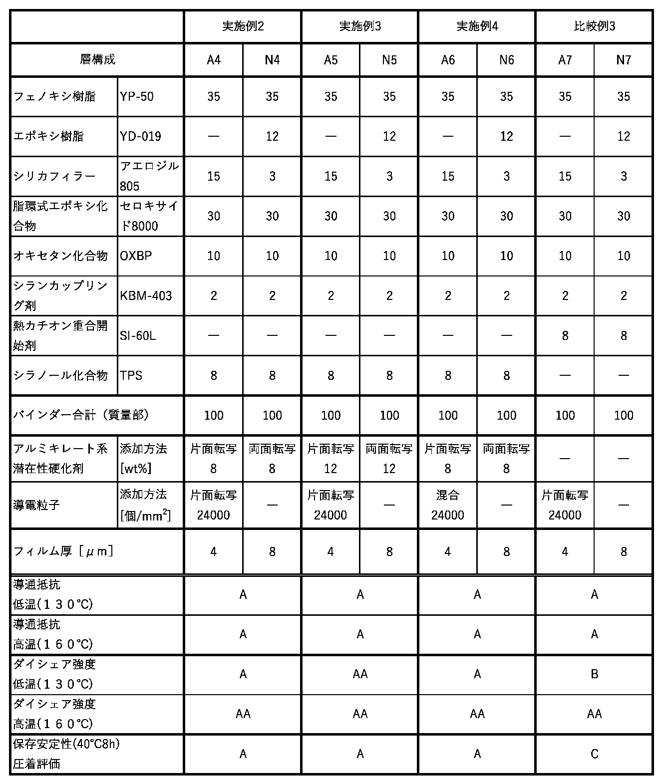
- Conductive particle-containing layer A1 The materials shown in Table 1 were mixed in the presence of a solvent such as propylene glycol monomethyl ether acetate (PMA) to obtain a binder composition.
- a solvent such as propylene glycol monomethyl ether acetate (PMA)
- This binder composition was applied onto a PET film using a bar coater and placed in an oven at a temperature of 80° C. The resulting mixture was dried for 5 minutes to form a binder layer having a thickness of 4 ⁇ m on the PET film.
- PMA propylene glycol monomethyl ether acetate
- Conductive particles were filled into the recesses of a transfer substrate with a particle density of 24,000 particles/ mm2 , one side of a binder layer was placed on top of the conductive particles, and pressure was applied (conditions: temperature 40-50°C, pressure 0.5 MPa) to attach the conductive particles to the surface of the binder layer. The binder layer was then peeled off from the transfer substrate, and the conductive particles on the binder layer were pressed (conditions: temperature 40-50°C, pressure 0.5 MPa) to push them into the binder layer, thereby disposing the conductive particles on one side of the binder layer.
- a transfer substrate with recesses formed at a predetermined density was used, and the recesses were filled with aluminum chelate-based latent hardener so that the amount of aluminum chelate-based latent hardener in the film layer was 4 wt %, and the aluminum chelate-based latent hardener was removed from areas other than the recesses with a squeegee.
- One side of the binder layer was placed on the transfer substrate with the aluminum chelate-based latent hardener filled in the recesses, and pressure was applied (conditions: temperature 40-50°C, pressure 0.5 MPa) to attach the aluminum chelate-based latent hardener to the surface of the binder layer.
- the binder layer was then peeled off from the transfer substrate, and the aluminum chelate-based latent hardener on the binder layer was pressurized (conditions: temperature 40-50°C, pressure 0.5 MPa) and pressed into the binder layer, disposing the aluminum chelate-based latent hardener on the other side of the binder layer to produce a conductive particle-containing layer A1.
- a transfer substrate with recesses formed at a predetermined density was used, and the recesses were filled with aluminum chelate-based latent hardener so that the amount of aluminum chelate-based latent hardener in the film layer was 4 wt %, and the aluminum chelate-based latent hardener was removed from areas other than the recesses with a squeegee.
- One side of the binder layer was placed on the transfer substrate with the aluminum chelate-based latent hardener filled in the recesses, and pressure was applied (conditions: temperature 40-50°C, pressure 0.5 MPa) to attach the aluminum chelate-based latent hardener to the surface of the binder layer.
- the binder layer was then peeled off from the transfer substrate, and the aluminum chelate-based latent hardener on the binder layer was pressurized (conditions: temperature 40-50°C, pressure 0.5 MPa) and pressed into the binder layer, thereby disposing the aluminum chelate-based latent hardener on one side of the binder layer. Similarly, aluminum chelate-based latent hardener was disposed on the other side of the binder layer to produce a conductive particle-free layer N1.
- Table 1 shows the evaluation results of the conduction resistance, die shear strength, and storage stability of Example 1.
- Example 1 the aluminum chelate-based latent hardener is placed after film formation, suppressing the effects of the solvent and allowing excellent conduction resistance, die shear strength, and storage stability to be obtained.
- the cross section of the two-layer anisotropic conductive film produced in Example 1 was observed with an electron microscope, the maximum distance in the film thickness direction between adjacent latent hardeners was approximately 5 ⁇ m in the conductive particle-free layer N1.
- Comparative Example 1 a film layer of a curing agent-free adhesive composition not containing a curing agent was formed, and a latent curing agent was sprinkled on the surface of the film layer to produce a conductive particle-containing layer A2. Similarly, a film layer of a curing agent-free adhesive composition not containing a curing agent was formed, and a latent curing agent was sprinkled on the surface of the film layer to produce a conductive particle-free layer N2. Then, the conductive particle-free layer N2 was laminated on the surface of the conductive particle-containing layer A2 on which the aluminum chelate-based latent curing agent was sprinkled, to produce a two-layer anisotropic conductive film.
- Conductive particle-containing layer A2 The materials shown in Table 1 were mixed in the presence of a solvent such as propylene glycol monomethyl ether acetate (PMA) to obtain a binder composition.
- a solvent such as propylene glycol monomethyl ether acetate (PMA)
- PMA propylene glycol monomethyl ether acetate
- This binder composition was applied onto a PET film using a bar coater and placed in an oven at a temperature of 80° C. The resulting mixture was dried for 5 minutes to form a binder layer having a thickness of 4 ⁇ m on the PET film.
- Conductive particles were filled into the recesses of a transfer substrate with a particle density of 24,000 particles/ mm2 , one side of a binder layer was placed on top of the conductive particles, and pressure was applied (conditions: temperature 40-50°C, pressure 0.5 MPa) to attach the conductive particles to the surface of the binder layer. The binder layer was then peeled off from the transfer substrate, and the conductive particles on the binder layer were pressed (conditions: temperature 40-50°C, pressure 0.5 MPa) to push them into the binder layer, thereby disposing the conductive particles on one side of the binder layer.
- the aluminum chelate-based latent hardener was sprinkled onto the other side of the binder layer so that the amount of aluminum chelate-based latent hardener was 4 wt%, and the aluminum chelate-based latent hardener was attached to the surface of the binder layer.
- the aluminum chelate-based latent hardener on the binder layer was then pressurized (conditions: temperature 40-50°C, pressure 0.5 MPa) and pushed into the binder layer, disposing the aluminum chelate-based latent hardener on the other side of the binder layer and creating conductive particle-containing layer A2.
- Example 2 shows the evaluation results of the electrical conduction resistance, die shear strength, and storage stability of Example 2.
- Example 2 an aluminum chelate-based latent hardener is placed after film formation, suppressing the effects of the solvent and allowing excellent electrical conduction resistance, die shear strength, and storage stability to be obtained.
- the die shear strength at high temperatures was superior to that of Example 1.
- Example 3 In Example 3, a conductive particle-containing layer A5 was prepared in the same manner as the conductive particle-containing layer A1, except that a transfer substrate was used in which recesses were formed at a predetermined number density so that the amount of the aluminum chelate-based latent curing agent in the film layer was 12 wt%.
- a conductive particle-free layer N5 was prepared in the same manner as the conductive particle-free layer N1, except that a transfer substrate was used in which recesses were formed at a predetermined number density so that the amount of the aluminum chelate-based latent curing agent in the film layer was 12 wt%. Then, a conductive particle-free layer N5 was laminated on the transfer surface of the aluminum chelate-based latent curing agent of the conductive particle-containing layer A5, to prepare a two-layer anisotropic conductive film.
- Example 3 shows the evaluation results of the electrical resistance, die shear strength, and storage stability of Example 3.
- an aluminum chelate-based latent hardener is placed after film formation, suppressing the effects of the solvent and allowing excellent electrical resistance, die shear strength, and storage stability to be obtained.
- the die shear strength at high and low temperatures was superior to that of Example 1.
- Example 4 In Example 4, the materials shown in Table 2 were mixed in the presence of a solvent of propylene glycol monomethyl ether acetate (PMA), and a predetermined amount of conductive particles was further mixed so that the number density was 24,000 particles/ mm2 to obtain a binder composition.
- This binder composition was applied to a PET film with a bar coater and dried in an oven at a temperature of 80°C for 5 minutes to form a binder layer having a thickness of 4 ⁇ m on the PET film.
- PMA propylene glycol monomethyl ether acetate
- a conductive particle-containing layer A6 was produced in the same manner as the conductive particle-containing layer A1, except that a transfer substrate was used in which recesses were formed at a predetermined number density so that the amount of the aluminum chelate-based latent curing agent in the film layer was 8 wt%.
- a non-conductive particle-containing layer N6 was prepared in the same manner as the non-conductive particle-containing layer N1, except that a transfer substrate was used in which recesses were formed at a predetermined number density so that the amount of aluminum chelate-based latent hardener in the film layer was 8 wt %. Then, the non-conductive particle-containing layer N6 was laminated on the transfer surface of the aluminum chelate-based latent hardener of the conductive particle-containing layer A6, to prepare a two-layer anisotropic conductive film.
- Example 4 shows the evaluation results of the electrical conduction resistance, die shear strength, and storage stability of Example 4.
- Example 4 an aluminum chelate-based latent hardener is placed after film formation, suppressing the effects of the solvent and allowing excellent electrical conduction resistance, die shear strength, and storage stability to be obtained.
- the die shear strength at high temperatures was superior to that of Example 1.
- Comparative Example 3 a conductive particle-containing layer A7 and a conductive particle-free layer N7 were prepared using a thermal cationic polymerization initiator instead of a silanol compound and an aluminum chelate-based latent curing agent.
- the materials shown in Table 2 were mixed in the presence of a solvent such as propylene glycol monomethyl ether acetate (PMA) to obtain a binder composition.
- PMA propylene glycol monomethyl ether acetate
- This binder composition was applied to a PET film using a bar coater and dried in an oven at a temperature of 80° C. for 5 minutes to form a binder layer having a thickness of 4 ⁇ m on the PET film.
- the materials shown in Table 1 were mixed in the presence of a solvent, propylene glycol monomethyl ether acetate (PMA), to obtain a binder composition.
- This binder composition was applied to a PET film with a bar coater and dried in an oven at 80°C for 5 minutes to form a binder layer with a thickness of 8 ⁇ m on the PET film, producing a conductive particle-free layer N7.
- the conductive particle-containing layer A7 and the conductive particle-free layer N7 were then laminated together to produce a two-layer anisotropic conductive film.
- Table 2 shows the evaluation results of the conduction resistance, die shear strength, and storage stability of Comparative Example 3.
- Comparative Example 3 a thermocationic curing agent with high solvent resistance was used, so an anisotropic conductive film could be produced, but the die shear strength at low temperature bonding was small and the storage stability was also low. This is thought to be due to the effect of the solvent on the curing agent during film formation.
Landscapes
- Chemical & Material Sciences (AREA)
- Organic Chemistry (AREA)
- Chemical Kinetics & Catalysis (AREA)
- Health & Medical Sciences (AREA)
- Medicinal Chemistry (AREA)
- Polymers & Plastics (AREA)
- Adhesives Or Adhesive Processes (AREA)
- Adhesive Tapes (AREA)
- Laminated Bodies (AREA)
Abstract
Description
[1]
硬化剤を含まない硬化剤非含有接着剤組成物のフィルム層を成形する成形工程と、
潜在性硬化剤が配置された転写基板から前記フィルム層に潜在性硬化剤を転写し、前記潜在性硬化剤を、前記フィルム層の少なくとも一方の面から露出させるか、又は前記フィルム層の少なくとも一方の面に近接させて配置する配置工程と
を有する接着フィルムの製造方法。
[2]
前記潜在性硬化剤が、前記フィルム層に塊状で配置される請求項[1]記載の接着フィルムの製造方法。
[3]
前記潜在性硬化剤が、マイクロカプセル型である[1]又は[2]記載の接着フィルムの製造方法。
[4]
前記硬化剤非含有接着剤組成物が、膜形成樹脂と、カチオン重合性化合物と、シラン系化合物とを含み、
前記潜在性硬化剤が、アルミニウムキレート系潜在性硬化剤である[1]又は[2]記載の接着フィルムの製造方法。
[5]
前記フィルム層に導電粒子を配置する導電粒子配置工程をさらに有する[1]又は[2]記載の接着フィルムの製造方法。
[6]
前記成形工程では、前記硬化剤非含有接着剤組成物に導電粒子を配合し、導電粒子を含有するフィルム層を成形する[1]又は[2]記載の接着フィルムの製造方法。
[7]
潜在性硬化剤が、少なくとも一方の面から露出するか、又は少なくとも一方の面に近接して配置されてなる接着剤組成物のフィルム層を有し、
前記潜在性硬化剤の平均粒径が、2μm以上50μm以下であり、
前記フィルム層の厚みが、3μm以上40μm以下である接着フィルム。
[8]
潜在性硬化剤が、少なくとも一方の面から露出するか、又は少なくとも一方の面に近接して配置され、導電粒子を含有するフィルム層を有し、
前記潜在性硬化剤の平均粒径が、2μm以上50μm以下であり、
前記フィルム層の厚みが、3μm以上40μm以下である導電フィルム。
[9]
潜在性硬化剤が、少なくとも一方の面から露出するか、又は少なくとも一方の面に近接して配置され、導電粒子を含有するフィルム層を有し、
前記潜在性硬化剤の平均粒径が、2μm以上50μm以下であり、
前記フィルム層の厚みが、3μm以上40μm以下である異方性導電フィルム。
[10]
前記[7]記載の接着フィルムを介して、第1の部品と第2の部品とを接着する構造体の製造方法。
[11]
前記[7]記載の接着フィルム、前記[8]記載の導電フィルム、又は前記[9]記載の異方性導電フィルムを介して、第1の部品の端子と第2の部品の端子とを接続する接続構造体の製造方法。
[12]
前記[7]記載の接着フィルムを介して、第1の部品と第2の部品とが接着された構造体。
[13]
前記[7]記載の接着フィルム、前記[8]記載の導電フィルム、又は前記[9]記載の異方性導電フィルムを介して、第1の電子部品の端子と第2の電子部品の端子とが接続された接続構造体。
1.接着フィルムの製造方法
2.接着フィルム
3.構造体の製造方法及び構造体
4.実施例
本実施の形態に係る接着フィルムの製造方法は、硬化剤を含まない硬化剤非含有接着剤組成物のフィルム層を成形する成形工程と、潜在性硬化剤が配置された転写基板から前記フィルム層に潜在性硬化剤を転写し、前記潜在性硬化剤を、前記フィルム層の少なくとも一方の面から露出させるか、又は前記フィルム層の少なくとも一方の面に近接させて配置する配置工程とを有するものである。これにより、潜在性硬化剤の溶剤による硬化反応の進行を抑制し、優れた保存安定性を得ることができる。
成形工程(A)では、先ず、硬化剤を含まない硬化剤非含有接着剤組成物を調整する。接着剤組成物は、公知の絶縁性バインダーを用いることができる。硬化型としては、熱硬化型、光硬化型、光熱併用硬化型などが挙げられ、例えば、エポキシ化合物と熱カチオン重合開始剤とを含む熱カチオン重合型樹脂組成物、エポキシ化合物と熱アニオン重合開始剤とを含む熱アニオン重合型樹脂組成物、(メタ)アクリレート化合物と光ラジカル重合開始剤とを含む光ラジカル重合型樹脂組成物、(メタ)アクリレート化合物と熱ラジカル重合開始剤とを含む熱ラジカル重合型樹脂組成物などが挙げられる。すなわち、硬化剤非含有接着剤組成物は、例えば熱カチオン重合型樹脂組成物の場合、熱カチオン重合開始剤を含まずに、エポキシ化合物などのカチオン重合性化合物を含むものである。
配置工程(B)では、先ず、フィルム層12の第1面12Aに潜在性硬化剤13を保持させる。潜在性硬化剤13を保持させる方法としては、転写基板20を用いてフィルム層12に潜在性硬化剤13を転写する転写方法、フィルム層12に潜在性硬化剤13を散布する散布方法などが挙げられる。これらの中でも転写方法は、潜在性硬化剤を平面視で均一に配置することができ、また転写後に平板等で押込めば厚み方向の位置も均一に配置することができるため、優れた接着強度(ダイシェア強度、ピール強度)を得ることができる。
本実施の形態に係る接着フィルムは、潜在性硬化剤が、少なくとも一方の面から露出するか、又は少なくとも一方の面に近接して配置されてなる接着剤組成物のフィルム層を有するものである。潜在性硬化剤がフォルム層の表面に配置されることにより、硬化反応が開始され、優れた接着強度(ダイシェア強度、ピール強度)を得ることができる。
膜形成樹脂は、例えば平均分子量が10000以上の高分子量樹脂に相当し、フィルム形成性の観点から、10000~80000程度の平均分子量であることが好ましい。膜形成樹脂としては、フェノキシ樹脂、エポキシ樹脂、ポリエステル樹脂、ポリウレタン樹脂、ポリエステルウレタン樹脂、アクリル樹脂、ポリイミド樹脂、ブチラール樹脂等の種々の樹脂が挙げられ、これらは単独で用いてもよく、2種類以上を組み合わせて用いてもよい。これらの中でも、膜形成状態、接続信頼性等の観点からフェノキシ樹脂を好適に用いることが好ましい。膜形成樹脂の含有量は、好ましくは20~80wt%、より好ましくは30~60wt%である。
カチオン重合性化合物としては、エポキシ化合物、オキセタン化合物から選択される少なくとも1種を用いることができる。
アルミニウムキレート系潜在性硬化剤としては、例えば、アルミニウムキレート系硬化剤が、多官能イソシアネート化合物を界面重合させると同時に、ラジカル重合開始剤の存在下でラジカル重合性化合物をラジカル重合させて得た多孔性樹脂に保持されているものなどが挙げられる。
シラン系化合物は、アルミニウムキレート系硬化剤と共働してカチオン重合を開始させ、硬化を促進させることができる。シラン系化合物としては、高立体障害性のシラノール化合物、分子中に1~3の低級アルコキシ基を有するシランカップリング剤などを挙げることができる。
また、熱カチオン重合型樹脂組成物は、無機フィラーを含有することが好ましい。無機フィラーとしては、シリカ、タルク、酸化チタン、炭酸カルシウム、酸化マグネシウム等を用いることができる。無機フィラーは、単独でも2種類以上を併用してもよい。無機フィラーの含有量は、好ましくは1~50wt%、より好ましくは3~20wt%である。また、熱カチオン重合型樹脂組成物は、必要に応じて、顔料、帯電防止剤などを含有させることができる。
図5は、第1の形態の接着フィルムを模式的に示す断面図である。図5に示すように、第1の形態の接着フィルムは、潜在性硬化剤33が、第1面32Aから露出するか、又は少なくとも第1面32Aに近接して配置されてなる接着剤組成物のフィルム層32を有する。
図7は、第2の形態の接着フィルムを模式的に示す断面図である。図7に示すように、第2の形態の接着フィルムは、潜在性硬化剤43Aが、第1面42Aから露出するか、又は第1面42Aに近接して配置されてなり、潜在性硬化剤43Bが、第2面42Bから露出するか、又は第2面42Bに近接して配置されてなる接着剤組成物のフィルム層42を有する。
図8は、第3の形態の接着フィルムを模式的に示す断面図である。図8に示すように、第3の形態の接着フィルムは、潜在性硬化剤53Aが、第1面52Aから露出するか、又は第1面52Aに近接して配置されてなり、導電粒子54が、第2面52Bから露出するか、又は第2面52Bに近接して配置されてなる接着剤組成物のフィルム層52を有する。また、第3の形態の接着フィルムは、潜在性硬化剤43Aが、第1面42Aから露出するか、又は第1面42Aに近接して配置されてなり、潜在性硬化剤43Bが、第2面42Bから露出するか、又は第2面42Bに近接して配置されてなる接着剤組成物のフィルム層42を有する。すなわち、第3の形態の接着フィルムは、フィルム層52の第1面52Aにフィルム層42を積層したものである。なお、フィルム層42は、第2の形態と同様であるため、説明を省略する。
本実施の形態に係る接続体の製造方法は、前述した接着フィルムを介して、第1の部品と第2の部品とを接着するものであり、本実施の形態に係る接続体は、前述した接着フィルムを介して、第1の部品と第2の部品とが接着されてなるものである。また、接着フィルムは、導電フィルム又は異方性導電フィルムであってもよく、導電フィルム又は異方性導電フィルムを介して、第1の電子部品の端子と第2の電子部品の端子とを接続する接続構造体の製造方法であっても、導電フィルム又は異方性導電フィルムを介して、第1の電子部品の端子と第2の電子部品の端子とが接続された接続構造体であってもよい。
本実施例では、接着フィルムの一形態として導電粒子を含有する異方性導電フィルムを作製した。そして、異方性導電フィルムを用いて接続構造体を作製し、導通抵抗、接着強度、及び保存安定性について評価した。
下記材料を用いて異方性導電フィルムを作製した。フィルムのサイズは、20cm×30cmの大きさとした。
フェノキシ樹脂:YP50、日鉄ケミカル&マテリアル(株)
エポキシ樹脂:YD-019、日鉄ケミカル&マテリアル(株)
シリカフィラー:アエロジル805、日本アエロジル(株)
脂環式エポキシ樹脂:セロキサイド8000、(株)ダイセル
オキセタン化合物:OXBP、UBE(株)
シランカップリング剤:KBM-403、信越化学工業(株)
熱カチオン硬化剤:SI-60L、三新化学工業(株)
シラノール化合物:トリス(tert-ペントキシ)シラノール(TPS)
導電粒子(樹脂コア金属被覆導電粒子):AUL704、積水化学工業(株)、4μmφ
蒸留水800質量部と、界面活性剤(ニューレックスR-T、日油(株))0.05質量部と、分散剤としてポリビニルアルコール(PVA-205、(株)クラレ)4質量部とを、温度計を備えた3リットルの界面重合容器に入れ、均一に混合し水相を調製した。
所定の個数密度(12000個/mm2、24000個/mm2、36000個/mm2)の凸部を有する正方格子配列の金型を作製した。金型に透明性樹脂のペレットを溶融させた状態で流し込み、冷やして固めることにより、所定の個数密度12000個/mm2、24000個/mm2、36000個/mm2)の凹部を有する正方格子配列の転写基板を作製した。
下記に示す評価用ICと、ガラス基板を準備した。
(導通特性の評価用IC)
外形 1.8×20.0mm
厚み 0.5mm
バンプ仕様 サイズ30×85μm、バンプ間距離50μm、バンプ高さ9μm
(ガラス基板)
ガラス材質 コーニング社製1737F
外形 30×50mm
厚み 0.5mm
電極 ITO配線
温度130℃又は温度160℃の圧着条件で作製した接続構造体について、デジタルマルチメータ(34401A、アジレント・テクノロジー株式会社製)を用いて4端子法にて電流1mAを流したときの抵抗値(Ω)を測定した。導通抵抗の評価は、実施例又は比較例の接続構造体(N=10)を次の基準で行い、最も低い評価を実施例又は比較例の評価とした。
A:抵抗値の最大値が2Ω未満
B:抵抗値の最大値が2Ω以上4Ω以下
C:抵抗値の最大値が4Ω超
温度130℃又は温度160℃の圧着条件で作製した接続構造体について、ダイシェアテスタ(4000series、ノードソン・アドバンスト・テクノロジー(株))を用いて、ツールスピード0.2mm/秒の条件で、評価用ICのダイシェア強度を測定した。ダイシェア強度の評価は、実施例又は比較例の接続構造体(N=10)を次の基準で行い、最も低い評価を実施例又は比較例の評価とした。
AA:ダイシェア強度が900N超
A:ダイシェア強度が600N以上900N以下
B:ダイシェア強度が300N以上600N以下
C:ダイシェア強度が300N未満
温度40℃-時間8hの環境条件で異方性導電フィルムをエージング処理した。エージング処理した異方性導電フィルムを用いて、前述した接続構造体の作製方法と同様に、温度130℃-圧力70MPa-時間5secの圧着条件で接続構造体を作製した。そして、エージング処理した異方性導電フィルムを用いて接続した接続構造体について、前述したダイシェア強度の評価と同様に、ダイシェア強度を測定した。保存安定性の評価は、エージング処理していない異方性導電フィルムを用いて接続した接続構造体のダイシェア強度に対し、実施例又は比較例の接続構造体(N=10)を次の基準で行い、最も低い評価を実施例又は比較例の評価とした。
AA:ダイシェア強度の低下が10%未満
A:ダイシェア強度の低下が10%以上30%以下
B:ダイシェア強度の低下が30%以上50%以下
C:ダイシェア強度の低下が50%超
実施例1では、硬化剤を含まない硬化剤非含有接着剤組成物のフィルム層を成形し、潜在性硬化剤が配置された転写基板を用いて、フィルム層に潜在性硬化剤を転写し、導電粒子含有層A1を作製した。同様に、硬化剤を含まない硬化剤非含有接着剤組成物のフィルム層を成形し、潜在性硬化剤が配置された転写基板を用いて、フィルム層に潜在性硬化剤を転写し、導電粒子非含有層N1を作製した。そして、導電粒子含有層A1のアルミニウムキレート系潜在性硬化剤の転写面に導電粒子非含有層N1を積層させ、2層型の異方性導電フィルムを作製した。
表1に示す材料をプロピレングリコールモノメチルエーテルアセテート(PMA)の溶剤存在下で混合し、バインダー組成物を得た。このバインダー組成物をPETフィルム上にバーコーターで塗布し、温度80℃のオーブンにて5分間乾燥させ、PETフィルム上に厚み4μmのバインダー層を形成した。
表1に示す材料をプロピレングリコールモノメチルエーテルアセテート(PMA)の溶剤存在下で混合し、バインダー組成物を得た。このバインダー組成物をPETフィルム上にバーコーターで塗布し、温度80℃のオーブンにて5分間乾燥させ、PETフィルム上に厚み8μmのバインダー層を形成した。
比較例1では、硬化剤を含まない硬化剤非含有接着剤組成物のフィルム層を成形し、潜在性硬化剤をフィルム層の表面に振掛け、導電粒子含有層A2を作製した。同様に、硬化剤を含まない硬化剤非含有接着剤組成物のフィルム層を成形し、潜在性硬化剤をフィルム層の表面に振掛け、導電粒子非含有層N2を作製した。そして、導電粒子含有層A2のアルミニウムキレート系潜在性硬化剤を振掛けた面に導電粒子非含有層N2を積層させ、2層型の異方性導電フィルムを作製した。
表1に示す材料をプロピレングリコールモノメチルエーテルアセテート(PMA)の溶剤存在下で混合し、バインダー組成物を得た。このバインダー組成物をPETフィルム上にバーコーターで塗布し、温度80℃のオーブンにて5分間乾燥させ、PETフィルム上に厚み4μmのバインダー層を形成した。
表1に示す材料をプロピレングリコールモノメチルエーテルアセテート(PMA)の溶剤存在下で混合し、バインダー組成物を得た。このバインダー組成物をPETフィルム上にバーコーターで塗布し、温度80℃のオーブンにて5分間乾燥させ、PETフィルム上に厚み8μmのバインダー層を形成した。
比較例2では、表1に示すように、アルミニウムキレート系潜在性硬化剤とシラノール化合物とを混合した接着剤組成物を作製し、導電粒子含有層A3の作製及び導電粒子非含有層N3の作製を試みた。しかしながら、比較例2では、導電粒子含有層A3の作製及び導電粒子非含有層N3の作製において、混合時にアルミニウムキレート系潜在性硬化剤が溶剤と反応し、発熱、硬化してしまうため、フィルム状に形成することができなかった。

実施例2では、フィルム層中のアルミニウムキレート系潜在性硬化剤の配合量が8wt%となるように、所定の個数密度で凹部が形成された転写基板を用いた以外は、導電粒子含有層A1と同様に、導電粒子含有層A4を作製した。また、フィルム層中のアルミニウムキレート系潜在性硬化剤の配合量が8wt%となるように、所定の個数密度で凹部が形成された転写基板を用いた以外は、導電粒子非含有層N1と同様に、導電粒子非含有層N4を作製した。そして、導電粒子含有層A4のアルミニウムキレート系潜在性硬化剤の転写面に導電粒子非含有層N4を積層させ、2層型の異方性導電フィルムを作製した。
実施例3では、フィルム層中のアルミニウムキレート系潜在性硬化剤の配合量が12wt%となるように、所定の個数密度で凹部が形成された転写基板を用いた以外は、導電粒子含有層A1と同様に、導電粒子含有層A5を作製した。また、フィルム層中のアルミニウムキレート系潜在性硬化剤の配合量が12wt%となるように、所定の個数密度で凹部が形成された転写基板を用いた以外は、導電粒子非含有層N1と同様に、導電粒子非含有層N5を作製した。そして、導電粒子含有層A5のアルミニウムキレート系潜在性硬化剤の転写面に導電粒子非含有層N5を積層させ、2層型の異方性導電フィルムを作製した。
実施例4では、表2に示す材料をプロピレングリコールモノメチルエーテルアセテート(PMA)の溶剤存在下で混合し、さらに個数密度が24000個/mm2となるように所定量の導電粒子を混合し、バインダー組成物を得た。このバインダー組成物をPETフィルム上にバーコーターで塗布し、温度80℃のオーブンにて5分間乾燥させ、PETフィルム上に厚み4μmのバインダー層を形成した。そして、フィルム層中のアルミニウムキレート系潜在性硬化剤の配合量が8wt%となるように、所定の個数密度で凹部が形成された転写基板を用いた以外は、導電粒子含有層A1と同様に、導電粒子含有層A6を作製した。
比較例3では、シラノール化合物及びアルミニウムキレート系潜在性硬化剤の代わりに、熱カチオン重合開始剤を用いて導電粒子含有層A7及び導電粒子非含有層N7を作製した。表2に示す材料をプロピレングリコールモノメチルエーテルアセテート(PMA)の溶剤存在下で混合し、バインダー組成物を得た。このバインダー組成物をPETフィルム上にバーコーターで塗布し、温度80℃のオーブンにて5分間乾燥させ、PETフィルム上に厚み4μmのバインダー層を形成した。
Claims (13)
- 硬化剤を含まない硬化剤非含有接着剤組成物のフィルム層を成形する成形工程と、
潜在性硬化剤が配置された転写基板から前記フィルム層に潜在性硬化剤を転写し、前記潜在性硬化剤を、前記フィルム層の少なくとも一方の面から露出させるか、又は前記フィルム層の少なくとも一方の面に近接させて配置する配置工程と
を有する接着フィルムの製造方法。 - 前記潜在性硬化剤が、前記フィルム層に塊状で配置される請求項1記載の接着フィルムの製造方法。
- 前記潜在性硬化剤が、マイクロカプセル型である請求項1又は2記載の接着フィルムの製造方法。
- 前記硬化剤非含有接着剤組成物が、膜形成樹脂と、カチオン重合性化合物と、シラン系化合物とを含み、
前記潜在性硬化剤が、アルミニウムキレート系潜在性硬化剤である請求項1又は2記載の接着フィルムの製造方法。 - 前記フィルム層に導電粒子を配置する導電粒子配置工程をさらに有する請求項1又は2記載の接着フィルムの製造方法。
- 前記成形工程では、前記硬化剤非含有接着剤組成物に導電粒子を配合し、導電粒子を含有するフィルム層を成形する請求項1又は2記載の接着フィルムの製造方法。
- 潜在性硬化剤が、少なくとも一方の面から露出するか、又は少なくとも一方の面に近接して配置されてなる接着剤組成物のフィルム層を有し、
前記潜在性硬化剤の平均粒径が、2μm以上50μm以下であり、
前記フィルム層の厚みが、3μm以上40μm以下である接着フィルム。 - 潜在性硬化剤が、少なくとも一方の面から露出するか、又は少なくとも一方の面に近接して配置され、導電粒子を含有するフィルム層を有し、
前記潜在性硬化剤の平均粒径が、2μm以上50μm以下であり、
前記フィルム層の厚みが、3μm以上40μm以下である導電フィルム。 - 潜在性硬化剤が、少なくとも一方の面から露出するか、又は少なくとも一方の面に近接して配置され、導電粒子を含有するフィルム層を有し、
前記潜在性硬化剤の平均粒径が、2μm以上50μm以下であり、
前記フィルム層の厚みが、3μm以上40μm以下である異方性導電フィルム。 - 前記請求項7記載の接着フィルムを介して、第1の部品と第2の部品とを接着する構造体の製造方法。
- 前記請求項7記載の接着フィルム、前記請求項8記載の導電フィルム、又は前記請求項9記載の異方性導電フィルムを介して、第1の部品の端子と第2の部品の端子とを接続する接続構造体の製造方法。
- 前記請求項7記載の接着フィルムを介して、第1の部品と第2の部品とが接着された構造体。
- 前記請求項7記載の接着フィルム、前記請求項8記載の導電フィルム、又は前記請求項9記載の異方性導電フィルムを介して、第1の電子部品の端子と第2の電子部品の端子とが接続された接続構造体。
Priority Applications (2)
| Application Number | Priority Date | Filing Date | Title |
|---|---|---|---|
| CN202480037272.0A CN121311557A (zh) | 2023-06-09 | 2024-05-23 | 粘接膜的制造方法及粘接膜、以及结构体的制造方法及结构体 |
| KR1020257040408A KR20260006638A (ko) | 2023-06-09 | 2024-05-23 | 접착 필름의 제조 방법 및 접착 필름, 그리고 구조체의 제조 방법 및 구조체 |
Applications Claiming Priority (2)
| Application Number | Priority Date | Filing Date | Title |
|---|---|---|---|
| JP2023095916A JP2024176983A (ja) | 2023-06-09 | 2023-06-09 | 接着フィルムの製造方法及び接着フィルム、並びに、構造体の製造方法及び構造体 |
| JP2023-095916 | 2023-06-09 |
Publications (1)
| Publication Number | Publication Date |
|---|---|
| WO2024252950A1 true WO2024252950A1 (ja) | 2024-12-12 |
Family
ID=93795477
Family Applications (1)
| Application Number | Title | Priority Date | Filing Date |
|---|---|---|---|
| PCT/JP2024/019117 Ceased WO2024252950A1 (ja) | 2023-06-09 | 2024-05-23 | 接着フィルムの製造方法及び接着フィルム、並びに、構造体の製造方法及び構造体 |
Country Status (5)
| Country | Link |
|---|---|
| JP (1) | JP2024176983A (ja) |
| KR (1) | KR20260006638A (ja) |
| CN (1) | CN121311557A (ja) |
| TW (1) | TW202506946A (ja) |
| WO (1) | WO2024252950A1 (ja) |
Citations (6)
| Publication number | Priority date | Publication date | Assignee | Title |
|---|---|---|---|---|
| WO2009005130A1 (ja) * | 2007-07-03 | 2009-01-08 | Hitachi Chemical Co., Ltd. | 接着剤組成物、接着剤組成物を用いた接着部材、半導体搭載用支持部材、半導体装置とそれらの製造方法 |
| JP2017088723A (ja) * | 2015-11-09 | 2017-05-25 | 日東電工株式会社 | 接着方法、接着構造体、および、接着キット |
| JP2017095570A (ja) * | 2015-11-20 | 2017-06-01 | 旭化成株式会社 | 接着フィルム用エポキシ樹脂組成物。 |
| JP2018172642A (ja) * | 2017-03-24 | 2018-11-08 | 日東電工株式会社 | 粘接着シート、接着キット、接着構造体およびその製造方法 |
| JP2021093357A (ja) * | 2019-12-03 | 2021-06-17 | デクセリアルズ株式会社 | 異方性導電フィルム |
| JP2023080000A (ja) * | 2021-11-29 | 2023-06-08 | デクセリアルズ株式会社 | 潜在性硬化剤及びその製造方法、並びに硬化性組成物 |
Family Cites Families (1)
| Publication number | Priority date | Publication date | Assignee | Title |
|---|---|---|---|---|
| JP6489494B2 (ja) | 2014-09-09 | 2019-03-27 | デクセリアルズ株式会社 | アルミニウムキレート系潜在性硬化剤、その製造方法及び熱硬化型エポキシ樹脂組成物 |
-
2023
- 2023-06-09 JP JP2023095916A patent/JP2024176983A/ja active Pending
-
2024
- 2024-05-23 CN CN202480037272.0A patent/CN121311557A/zh active Pending
- 2024-05-23 WO PCT/JP2024/019117 patent/WO2024252950A1/ja not_active Ceased
- 2024-05-23 KR KR1020257040408A patent/KR20260006638A/ko active Pending
- 2024-06-04 TW TW113120607A patent/TW202506946A/zh unknown
Patent Citations (6)
| Publication number | Priority date | Publication date | Assignee | Title |
|---|---|---|---|---|
| WO2009005130A1 (ja) * | 2007-07-03 | 2009-01-08 | Hitachi Chemical Co., Ltd. | 接着剤組成物、接着剤組成物を用いた接着部材、半導体搭載用支持部材、半導体装置とそれらの製造方法 |
| JP2017088723A (ja) * | 2015-11-09 | 2017-05-25 | 日東電工株式会社 | 接着方法、接着構造体、および、接着キット |
| JP2017095570A (ja) * | 2015-11-20 | 2017-06-01 | 旭化成株式会社 | 接着フィルム用エポキシ樹脂組成物。 |
| JP2018172642A (ja) * | 2017-03-24 | 2018-11-08 | 日東電工株式会社 | 粘接着シート、接着キット、接着構造体およびその製造方法 |
| JP2021093357A (ja) * | 2019-12-03 | 2021-06-17 | デクセリアルズ株式会社 | 異方性導電フィルム |
| JP2023080000A (ja) * | 2021-11-29 | 2023-06-08 | デクセリアルズ株式会社 | 潜在性硬化剤及びその製造方法、並びに硬化性組成物 |
Also Published As
| Publication number | Publication date |
|---|---|
| CN121311557A (zh) | 2026-01-09 |
| KR20260006638A (ko) | 2026-01-13 |
| TW202506946A (zh) | 2025-02-16 |
| JP2024176983A (ja) | 2024-12-19 |
Similar Documents
| Publication | Publication Date | Title |
|---|---|---|
| JP5825373B2 (ja) | 導電粒子配置シート及びその製造方法 | |
| JP5151902B2 (ja) | 異方導電性フィルム | |
| JP6161864B2 (ja) | 樹脂組成物、樹脂シート、プリプレグ、積層板、金属基板、及びプリント配線板 | |
| CN104106182B (zh) | 各向异性导电连接材料、连接结构体、连接结构体的制造方法和连接方法 | |
| TWI855294B (zh) | 接著劑組成物 | |
| JP5410387B2 (ja) | 導電性粒子及びその製造方法、並びに異方性導電フィルム、接合体、及び接続方法 | |
| EP2640173A2 (en) | Method for fabricating an electronic device | |
| KR101131162B1 (ko) | 저온 속경화형 이방 전도성 필름용 조성물 및 이를 이용한 저온 속경화형 이방 전도성 필름 | |
| US20120295098A1 (en) | Fixed-array anisotropic conductive film using surface modified conductive particles | |
| KR102161430B1 (ko) | 이방성 도전 필름, 접속 방법, 및 접합체 | |
| JP2014129544A (ja) | 接着剤組成物とその製造方法及び接着剤組成物を用いた接着部材とその製造方法、半導体搭載用支持部材とその製造方法並びに半導体装置とその製造方法 | |
| JP4148685B2 (ja) | 潜在性硬化剤、潜在性硬化剤の製造方法及び接着剤 | |
| CN105359354A (zh) | 导电性粘接膜的制造方法、导电性粘接膜、连接体的制造方法 | |
| JP2005200521A (ja) | 接着フィルム、接着フィルムの製造方法 | |
| JP2010261003A (ja) | 回路接続用フィルム接着剤の製造方法 | |
| KR102207300B1 (ko) | 이방성 도전 필름, 그의 경화물 및 그의 제조 방법 | |
| JP2024176983A (ja) | 接着フィルムの製造方法及び接着フィルム、並びに、構造体の製造方法及び構造体 | |
| WO2020203295A1 (ja) | 接着剤組成物 | |
| JP6271048B2 (ja) | 異方性導電フィルム、接続方法、及び接合体 | |
| WO2025022790A1 (ja) | 構造体の製造方法及び接着フィルム | |
| JP5630639B2 (ja) | フィルム状導電性接着剤 | |
| JP6894221B2 (ja) | 異方性導電フィルム、これを含む積層フィルム、およびこれらの製造方法 | |
| JP2006233202A (ja) | 回路接続用異方導電性接着フィルム | |
| WO2024090129A1 (ja) | 接続材料、接続構造体、及び接続構造体の製造方法 | |
| JP2006233201A (ja) | 異方性導電接着フィルム |
Legal Events
| Date | Code | Title | Description |
|---|---|---|---|
| 121 | Ep: the epo has been informed by wipo that ep was designated in this application |
Ref document number: 24819182 Country of ref document: EP Kind code of ref document: A1 |
|
| ENP | Entry into the national phase |
Ref document number: 1020257040408 Country of ref document: KR Free format text: ST27 STATUS EVENT CODE: A-0-1-A10-A15-NAP-PA0105 (AS PROVIDED BY THE NATIONAL OFFICE) |
|
| WWE | Wipo information: entry into national phase |
Ref document number: 1020257040408 Country of ref document: KR |
|
| NENP | Non-entry into the national phase |
Ref country code: DE |
|
| WWP | Wipo information: published in national office |
Ref document number: 1020257040408 Country of ref document: KR |
|
| 122 | Ep: pct application non-entry in european phase |
Ref document number: 24819182 Country of ref document: EP Kind code of ref document: A1 |