WO2024252608A1 - 電子デバイス及び電子デバイスの製造方法 - Google Patents
電子デバイス及び電子デバイスの製造方法 Download PDFInfo
- Publication number
- WO2024252608A1 WO2024252608A1 PCT/JP2023/021317 JP2023021317W WO2024252608A1 WO 2024252608 A1 WO2024252608 A1 WO 2024252608A1 JP 2023021317 W JP2023021317 W JP 2023021317W WO 2024252608 A1 WO2024252608 A1 WO 2024252608A1
- Authority
- WO
- WIPO (PCT)
- Prior art keywords
- superconducting wiring
- electronic device
- support member
- superconducting
- wiring
- Prior art date
- Legal status (The legal status is an assumption and is not a legal conclusion. Google has not performed a legal analysis and makes no representation as to the accuracy of the status listed.)
- Ceased
Links
Images














Classifications
-
- H—ELECTRICITY
- H10—SEMICONDUCTOR DEVICES; ELECTRIC SOLID-STATE DEVICES NOT OTHERWISE PROVIDED FOR
- H10N—ELECTRIC SOLID-STATE DEVICES NOT OTHERWISE PROVIDED FOR
- H10N60/00—Superconducting devices
- H10N60/10—Junction-based devices
- H10N60/12—Josephson-effect devices
-
- H—ELECTRICITY
- H10—SEMICONDUCTOR DEVICES; ELECTRIC SOLID-STATE DEVICES NOT OTHERWISE PROVIDED FOR
- H10N—ELECTRIC SOLID-STATE DEVICES NOT OTHERWISE PROVIDED FOR
- H10N60/00—Superconducting devices
- H10N60/01—Manufacture or treatment
- H10N60/0912—Manufacture or treatment of Josephson-effect devices
-
- H—ELECTRICITY
- H10—SEMICONDUCTOR DEVICES; ELECTRIC SOLID-STATE DEVICES NOT OTHERWISE PROVIDED FOR
- H10N—ELECTRIC SOLID-STATE DEVICES NOT OTHERWISE PROVIDED FOR
- H10N60/00—Superconducting devices
- H10N60/80—Constructional details
- H10N60/805—Constructional details for Josephson-effect devices
-
- H—ELECTRICITY
- H10—SEMICONDUCTOR DEVICES; ELECTRIC SOLID-STATE DEVICES NOT OTHERWISE PROVIDED FOR
- H10N—ELECTRIC SOLID-STATE DEVICES NOT OTHERWISE PROVIDED FOR
- H10N60/00—Superconducting devices
- H10N60/80—Constructional details
- H10N60/81—Containers; Mountings
- H10N60/815—Containers; Mountings for Josephson-effect devices
-
- H—ELECTRICITY
- H10—SEMICONDUCTOR DEVICES; ELECTRIC SOLID-STATE DEVICES NOT OTHERWISE PROVIDED FOR
- H10N—ELECTRIC SOLID-STATE DEVICES NOT OTHERWISE PROVIDED FOR
- H10N69/00—Integrated devices, or assemblies of multiple devices, comprising at least one superconducting element covered by group H10N60/00
Definitions
- This disclosure relates to electronic devices and methods for manufacturing electronic devices.
- Quantum computers may use electronic devices with quantum bits that include Josephson junction elements.
- Josephson junction elements are formed on a substrate such as a silicon substrate.
- the objective of this disclosure is to provide an electronic device and a method for manufacturing an electronic device that can suppress the effects of a two-level system.
- an electronic device having a substrate having a recess on a first surface, a first superconducting wiring having a portion in contact with the first surface, a second superconducting wiring intersecting with the first superconducting wiring in a plan view above the recess and having a portion in contact with the first surface, an insulating film provided between the first superconducting wiring and the second superconducting wiring, and a first support member provided within the recess and supporting at least one of the first superconducting wiring or the second superconducting wiring, wherein the area between the area where the first superconducting wiring and the second superconducting wiring intersect in a plan view and the bottom surface of the recess is hollow.
- This disclosure makes it possible to suppress the effects of two-level systems.
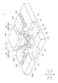
- FIG. 1 is a perspective view showing an electronic device according to a first embodiment.
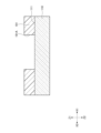
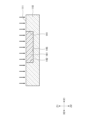
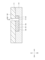
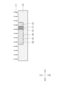
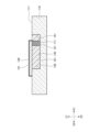
- FIG. 2 is a cross-sectional view (part 1) showing the electronic device according to the first embodiment.
- FIG. 3 is a cross-sectional view (part 2) showing the electronic device according to the first embodiment.
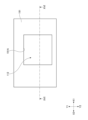
- FIG. 4 is a plan view (part 1) illustrating the method for manufacturing the electronic device according to the first embodiment.
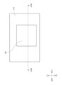
- FIG. 5 is a plan view (part 2) illustrating the method for manufacturing the electronic device according to the first embodiment.
- FIG. 6 is a plan view (part 3) illustrating the method for manufacturing the electronic device according to the first embodiment.
- FIG. 7 is a plan view (part 4) illustrating the method for manufacturing the electronic device according to the first embodiment.
- FIG. 1 is a perspective view showing an electronic device according to a first embodiment.
- FIG. 2 is a cross-sectional view (part 1) showing the electronic device according to the first embodiment.
- FIG. 3 is a cross-sectional view (part 2) showing the electronic device according to
- FIG. 8 is a plan view (part 5) illustrating the method for manufacturing the electronic device according to the first embodiment.
- FIG. 9 is a plan view (part 6) illustrating the method for manufacturing the electronic device according to the first embodiment.
- FIG. 10 is a plan view (part 7) illustrating the method for manufacturing the electronic device according to the first embodiment.
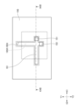
- FIG. 11 is a plan view (part 8) illustrating the method for manufacturing the electronic device according to the first embodiment.
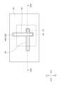
- FIG. 12 is a plan view (part 9) illustrating the method for manufacturing the electronic device according to the first embodiment.
- FIG. 13 is a plan view (part 10) illustrating the method for manufacturing the electronic device according to the first embodiment.
- FIG. 14 is a plan view (part 11) illustrating the method for manufacturing the electronic device according to the first embodiment.
- FIG. 15 is a cross-sectional view (part 1) illustrating the method for manufacturing the electronic device according to the first embodiment.
- 16A to 16C are cross-sectional views (part 2) illustrating the method for manufacturing the electronic device according to the first embodiment.
- FIG. 17 is a cross-sectional view (part 3) illustrating the method for manufacturing the electronic device according to the first embodiment.
- FIG. 18 is a cross-sectional view (part 4) illustrating the method for manufacturing the electronic device according to the first embodiment.
- FIG. 19 is a cross-sectional view (part 5) illustrating the method for manufacturing the electronic device according to the first embodiment.
- FIG. 20 is a cross-sectional view (part 6) illustrating the method for manufacturing the electronic device according to the first embodiment.
- FIG. 21 is a cross-sectional view (part 7) illustrating the method for manufacturing the electronic device according to the first embodiment.
- FIG. 22 is a cross-sectional view (part 8) illustrating the method for manufacturing the electronic device according to the first embodiment.
- FIG. 23 is a cross-sectional view (part 9) illustrating the method for manufacturing the electronic device according to the first embodiment.
- FIG. 24 is a cross-sectional view (part 10) illustrating the method for manufacturing the electronic device according to the first embodiment.
- FIG. 25 is a cross-sectional view (part 11) illustrating the method for manufacturing the electronic device according to the first embodiment.
- FIG. 26 is a perspective view showing an electronic device according to the second embodiment.
- FIG. 27 is a perspective view showing an electronic device according to the third embodiment.
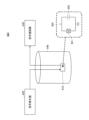
- FIG. 28 is a diagram illustrating a quantum processing device according to the fourth embodiment.
- the X1-X2 direction, the Y1-Y2 direction, and the Z1-Z2 direction are defined as mutually orthogonal directions.
- a plane including the X1-X2 direction and the Y1-Y2 direction is described as the XY plane
- a plane including the Y1-Y2 direction and the Z1-Z2 direction is described as the YZ plane
- a plane including the Z1-Z2 direction and the X1-X2 direction is described as the ZX plane.
- the Z1-Z2 direction is defined as the up-down direction, with the Z1 side as the top side and the Z2 side as the bottom side.
- a planar view refers to viewing an object from the Z1 side
- a planar shape refers to the shape of an object viewed from the Z1 side.
- FIG. 1 is a perspective view showing an electronic device according to the first embodiment.
- Figs. 2 and 3 are cross-sectional views showing the electronic device according to the first embodiment.
- the electronic device 1 has a substrate 110, a superconducting wiring 121, a superconducting wiring 122, an insulating film 130, a support member 151, and a support member 152.
- the substrate 110 is, for example, a silicon substrate or a sapphire substrate.
- a recess 112 is formed on the top surface 111 of the substrate 110.
- the top surface 111 is a surface parallel to the XY plane.
- the recess 112 has a rectangular planar shape with two sides parallel to the X1-X2 direction and two sides parallel to the Y1-Y2 direction. For example, the depth of the recess 112 (dimension in the Z1-Z2 direction) is constant.
- the recess 112 has sidewall surfaces 141 and 142 parallel to the YZ plane, sidewall surfaces 143 and 144 parallel to the ZX plane, and a bottom surface 145 parallel to the XY plane.
- the sidewall surface 141 is closer to the X1 side than the sidewall surface 142
- the sidewall surface 143 is closer to the Y1 side than the sidewall surface 144.
- the top surface 111 is an example of a first surface.
- the support members 151 and 152 are, for example, silicon oxide (SiO 2 ) films.
- the support members 151 and 152 are provided in the recessed portion 112.
- the height (thickness) of the support members 151 and 152 is preferably equal to the depth of the recessed portion 112, but may be greater or smaller than the depth of the recessed portion 112.
- the support member 151 is disposed near the side wall surface 141, and the support member 152 is disposed near the side wall surface 144.
- the distance between the support member 151 and the side wall surface 141 is smaller than the distance between the support member 151 and the side wall surface 142, and the distance between the support member 151 and the side wall surface 143 is larger than the distance between the support member 151 and the side wall surface 144.
- the distance between the support member 152 and the side wall surface 143 is greater than the distance between the support member 152 and the side wall surface 144, and the distance between the support member 152 and the side wall surface 141 is less than the distance between the support member 152 and the side wall surface 142.
- the distance between the support member 151 and the side wall surface 141 is less than the distance between the support member 152 and the side wall surface 141, and the distance between the support member 152 and the side wall surface 144 is less than the distance between the support member 151 and the side wall surface 144.
- the support member 151 is an example of a first support member
- the support member 152 is an example of a second support member.
- the superconducting wiring 121 and the superconducting wiring 122 are, for example, aluminum (Al) films.
- the superconducting wiring 121 extends along the X1-X2 direction. A portion of the superconducting wiring 121 contacts a portion of the upper surface 111 of the substrate 110 that is on the X2 side of the side wall surface 142. In a plan view, the superconducting wiring 121 is separated from the side wall surfaces 141, 143, and 144, and does not overlap with the side wall surfaces 141, 143, and 144.
- the X1 side end of the superconducting wiring 121 is supported by a support member 151.
- the superconducting wiring 122 extends along the Y1-Y2 direction.
- a portion of the superconducting wiring 122 contacts a portion of the upper surface 111 of the substrate 110 that is on the Y1 side of the side wall surface 143.
- the superconducting wiring 122 is separated from the side wall surfaces 141, 142, and 144 and does not overlap with the side wall surfaces 141, 142, and 144.
- the Y2 side end of the superconducting wiring 122 is supported by a support member 152.
- superconducting wiring 121 and superconducting wiring 122 cross each other. That is, in plan view, a portion of superconducting wiring 121 between support member 151 and side wall surface 142 and a portion of superconducting wiring 122 between support member 152 and side wall surface 143 overlap in the Z1-Z2 direction.
- Superconducting wiring 121 is an example of a first superconducting wiring
- superconducting wiring 122 is an example of a second superconducting wiring.
- the insulating film 130 is, for example, an aluminum oxide (Al 2 O 3 ) film.
- the insulating film 130 is provided between the superconducting wiring 121 and the superconducting wiring 122.
- the insulating film 130 is provided between the superconducting wiring 121 and the superconducting wiring 122 in a region where the superconducting wiring 121 and the superconducting wiring 122 overlap each other.
- the insulating film 130 contacts the superconducting wiring 121 and the superconducting wiring 122.
- the insulating film 130 may cover other parts of the superconducting wiring 121.
- the thickness of the insulating film 130 is a thickness that allows a tunnel effect to occur between the superconducting wiring 121 and the superconducting wiring 122.
- the insulating film 130 covers the top and side surfaces of the superconducting wiring 121, but is not shown in FIG. 1 except for the part between the superconducting wiring 121 and the superconducting wiring 122.
- the region where superconducting wiring 121 and superconducting wiring 122 intersect in a plan view functions as a superconducting Josephson junction element in an extremely low temperature environment of, for example, about 10 mK.
- a space 113 exists between the region that functions as a superconducting Josephson junction element and bottom surface 145 of recess 112.
- the region that functions as a superconducting Josephson junction element will be in direct contact with the substrate 110.
- the substrate 110 is a silicon substrate, an oxide will inevitably be present on the upper surface 111 due to natural oxidation.
- the oxide acts on the Josephson junction element as a defect called a two-level system (TLS), robbing the Josephson junction element of energy and shortening the coherence time of the quantum bit having the Josephson junction element. If the coherence time is shortened, the time for which the quantum entangled state is maintained will also be shortened, shortening the time for which quantum calculations can be performed in a quantum computer having quantum bits, and reducing fidelity.
- TLS two-level system
- the shapes of the superconducting wiring 121 and the superconducting wiring 122 are stable even above the recessed portion 112. Furthermore, since the material of the support member 151 and the support member 152, such as silicon oxide, has a lower dielectric constant than the material of the substrate 110, such as silicon, the parasitic capacitance between the superconducting wiring 121 and the substrate 110 and the parasitic capacitance between the superconducting wiring 122 and the substrate 110 can be kept low.
- the support member 151 and the support member 152 are separated from the Josephson junction element, so that the influence of the TLS present in the support member 151 and the support member 152 is unlikely to affect the Josephson junction element.
- the superconducting wiring 121 and the superconducting wiring 122 cross each other in a plan view, it is easy to form the superconducting wiring 121 and the superconducting wiring 122 with high precision, as described below.
- FIGS. 4 to 14 are plan views illustrating the method for manufacturing the electronic device according to the first embodiment.
- 15 to 25 are cross-sectional views showing the method for manufacturing the electronic device according to the first embodiment.
- a substrate 110 is prepared, and a mask 191 is formed on the upper surface 111 of the substrate 110.
- the mask 191 has an opening 191A that exposes the area in which the recessed portion 112 of the substrate 110 will be formed.
- the mask 191 is, for example, a resist mask.
- Fig. 15 corresponds to a cross-sectional view taken along line XV-XV in Fig. 4.
- FIG. 16 corresponds to a cross-sectional view taken along line XVI-XVI in FIG. 5.
- FIG. 17 corresponds to a cross-sectional view taken along the line XVII-XVII in FIG. 6.
- Fig. 18 corresponds to a cross-sectional view taken along line XVIII-XVIII in Fig. 7.
- a mask 192 is formed on the substrate 110 and the filling member 161.
- the mask 192 has an opening 192A exposing the region where the support member 151 is to be formed and an opening 192B exposing the region where the support member 152 is to be formed.
- the mask 192 is, for example, a resist mask.
- the portions of the filling member 161 exposed from the opening 192A and the portions exposed from the opening 192B are etched to form the openings 171 and 172 in the filling member 161.
- the opening 171 is connected to the opening 192A, and the opening 172 is connected to the opening 192B.
- the etching of the filling member 161 is, for example, dry etching.
- FIG. 19 corresponds to a cross-sectional view taken along the line XIX-XIX in FIG. 8.
- FIG. 20 corresponds to a cross-sectional view taken along the line XX-XX in FIG.
- the film 155 is etched back so that the film 155 remains in the openings 171 and 172.
- the support member 151 made of the film 155 is formed in the openings 171
- the support member 152 is formed in the openings 172.
- dry etching using, for example, tetrafluoromethane (CF 4 ) is performed.
- Fig. 21 corresponds to a cross-sectional view taken along the line XXI-XXI in Fig. 10.
- a mask 193 is formed on the substrate 110 and the embedding member 161.
- the mask 193 has a two-layer structure and includes a lower layer 194 and an upper layer 195.
- the lower layer 194 is formed on the substrate 110 and the embedding member 161, and the upper layer 195 is formed on the lower layer 194.
- the upper layer 195 includes an opening 195A that exposes the areas in which the superconducting wiring 121 and the superconducting wiring 122 are to be formed.
- the opening 195A has a cross-shaped planar shape.
- the lower layer 194 includes an opening 194A that is wider than the opening 195A.
- the opening 194A also has a cross-shaped planar shape.
- Fig. 22 corresponds to a cross-sectional view taken along the line XXII-XXII in Fig. 11.
- FIG. 12 and 23 corresponds to a cross-sectional view taken along the line XXIII-XXIII in Figure 12.
- Figure 24 corresponds to a cross-sectional view taken along the line XXIV-XXIV in Figure 13.
- the mask 193 is removed by, for example, a lift-off method. Then, the filling material 161 is removed.
- the filling material 161 is removed by, for example, dry etching using oxygen (O 2 ). At this time, by increasing the gas pressure, the filling material 161 below the superconducting wiring 121 and the superconducting wiring 122 can be easily removed.
- FIG. 25 corresponds to a cross-sectional view taken along the line XXV-XXV in FIG. 14.
- This manufacturing method uses the lift-off method, so the support member 151, the support member 152, the superconducting wiring 121, and the superconducting wiring 122 can be formed with high precision.
- the second embodiment differs from the first embodiment mainly in the structure of the superconducting wiring and the arrangement of the support members.
- the second embodiment relates to an electronic device.
- Fig. 26 is a perspective view showing an electronic device according to the second embodiment.
- the electronic device 2 has a substrate 210, a superconducting wiring 221, a superconducting wiring 222, an insulating film 230, two support members 251, two support members 252, four support members 253, and four support members 254.
- a structure having two support members 251, two support members 252, four support members 253, and four support members 254 is disclosed, but the number of each support member is not limited to this.
- the substrate 210 is, for example, a silicon substrate or a sapphire substrate.
- a recess 212 is formed on an upper surface 211 of the substrate 210.
- the upper surface 211 is a surface parallel to the XY plane.
- the recess 212 has a cross-shaped planar shape. For example, the depth of the recess 212 (dimension in the Z1-Z2 direction) is constant.
- the upper surface 211 is an example of a first surface.
- the support members 251, 252, 253, and 254 are, for example, SiO 2 films.
- the support members 251, 252, 253, and 254 are provided in the recessed portion 212.
- the height (thickness) of the support members 251, 252, 253, and 254 is preferably equal to the depth of the recessed portion 212, but may be greater or smaller than the depth of the recessed portion 212.
- the two support members 251 are arranged side by side in the X1-X2 direction in a portion of the recessed portion 212 that extends parallel to the X1-X2 direction.
- the four support members 253 are arranged on the X2 side of the two support members 251, and are arranged in a square lattice pattern parallel to the X1-X2 direction and the Y1-Y2 direction.
- the two support members 252 are arranged side by side in the Y1-Y2 direction in a portion of the recess 212 that extends parallel to the Y1-Y2 direction.
- the four support members 254 are arranged on the Y1 side of the two support members 252, and are arranged in a square lattice pattern parallel to the X1-X2 and Y1-Y2 directions.
- the superconducting wiring 221 and the superconducting wiring 222 are, for example, Al films.
- the superconducting wiring 221 extends along the X1-X2 direction.
- the superconducting wiring 221 has a thin wire portion 221A with a width W1A in the Y1-Y2 direction, and a thick wire portion 221B with a width W1B in the Y1-Y2 direction.
- the width W1B is greater than the width W1A.
- the thin wire portion 221A and the thick wire portion 221B are connected to each other.
- the thin wire portion 221A is supported by two support members 251, and the thick wire portion 221B is supported by four support members 253.
- the superconducting wiring 222 extends along the Y1-Y2 direction.
- the superconducting wiring 222 has a thin wire portion 222A with a width W2A in the X1-X2 direction, and a thick wire portion 222B with a width W2B in the X1-X2 direction. Width W2B is greater than width W2A.
- Thin line portion 222A and thick line portion 222B are connected to each other. Thin line portion 222A is supported by two support members 252, and thick line portion 222B is supported by four support members 254.
- Thin line portions 221A and 222A are an example of a first portion
- thick line portions 221B and 222B are an example of a second portion.
- the thin wire portion 221A of the superconducting wiring 221 and the thin wire portion 222A of the superconducting wiring 222 cross each other.
- the superconducting wiring 221 is an example of a first superconducting wiring
- the superconducting wiring 222 is an example of a second superconducting wiring.
- the insulating film 230 is, for example, an Al 2 O 3 film.
- the insulating film 230 is provided between the thin wire portion 221A and the thin wire portion 222A.
- the insulating film 230 is provided between the thin wire portion 221A and the thin wire portion 222A in the region where the thin wire portion 221A and the thin wire portion 222A overlap each other.
- the insulating film 230 contacts the thin wire portion 221A and the thin wire portion 222A.
- the insulating film 230 may cover other parts of the superconducting wiring 221.
- the thickness of the insulating film 230 is a thickness that can cause a tunnel effect between the thin wire portion 221A and the thin wire portion 222A.
- the insulating film 230 covers the upper surface and side surfaces of the superconducting wiring 221, but is omitted in FIG. 26 except for the portion between the superconducting wiring 121 and the superconducting wiring 122.
- the region where thin wire portion 221A and thin wire portion 222A intersect in a plan view functions as a superconducting Josephson junction element in an extremely low temperature environment of, for example, about 10 mK.
- a space 213 exists between the region that functions as a superconducting Josephson junction element and bottom surface 245 of recess 212.
- the electronic device 2 not only is there a hollow space between the region that functions as the superconducting Josephson junction element and the bottom surface 245 of the recessed portion 212, but also between the thick line portion 221B and the bottom surface 245, and between the thick line portion 222B and the bottom surface 245. This makes it possible to further reduce the parasitic capacitance between the superconducting wiring 221 and the substrate 210, and between the superconducting wiring 222 and the substrate 210.
- the thick line portion 221B and the thick line portion 222B are used for electrical connections with other elements, etc.
- the electronic device 2 according to the second embodiment can be manufactured by a method similar to that of the first embodiment.
- the electronic device 2 according to the second embodiment can be manufactured by changing the mask pattern used for etching from that of the first embodiment.
- the thick line portion 221B may be in contact with the upper surface 211 of the substrate 210, and the thick line portion 222B may be in contact with the upper surface 211 of the substrate 210.
- a third embodiment differs from the first embodiment mainly in the arrangement of the support members.
- Fig. 27 is a perspective view showing an electronic device according to the third embodiment.
- the electronic device 3 has a support member 351 instead of the support member 151, and has a support member 352 instead of the support member 152.
- the support members 351 and 352 are, for example, SiO 2 films. The thickness of the support members 351 and 352 is about 100 nm.
- the support members 351 and 352 are provided on the upper surface 111 of the substrate 110.
- the support member 351 is provided on a portion of the upper surface 111 of the substrate 110 that is closer to the X1 side than the side wall surface 141.
- the support member 352 is provided on a portion of the upper surface 111 of the substrate 110 that is closer to the Y2 side than the side wall surface 144.
- the end of the superconducting wiring 121 on the X1 side is supported by the support member 351.
- the end of the superconducting wiring 122 on the Y2 side is supported by the support member 352.
- the area that functions as a superconducting Josephson junction element and the bottom surface 145 of the recess 112 are hollow, so that the effect of TLS can be suppressed even if an oxide is present on the bottom surface 145.
- the dielectric constant of the support member is lower than that of the substrate, but the material of the support member is not limited to silicon oxide.
- the support member may contain silicon oxide, silicon nitride, aluminum oxide, or resin.
- An example of resin is benzocyclobutene (BCB).
- the material of the superconducting wiring is also not limited to aluminum.
- the superconducting wiring may contain a superconducting material other than Al, such as niobium (Nb), niobium nitride (NbN), tantalum (Ta), tantalum nitride (TaN), or titanium nitride (TiN).
- the material of the insulating film sandwiched between two superconducting wirings is not limited to aluminum oxide.
- the fourth embodiment relates to a quantum processing device including Josephson junction devices.
- Fig. 28 is a diagram showing a quantum processing device according to the fourth embodiment.
- the quantum computing device 800 has a quantum bit chip 810, a signal generator 820, a signal demodulator 830, and a cryogenic dilution refrigerator 840, as shown in FIG. 30.
- the quantum bit chip 810 is housed in the cryogenic dilution refrigerator 840 and cooled to a temperature of 10 mK or less.
- the signal generator 820 generates a microwave pulse signal, and the microwave pulse signal is input to the quantum bit chip 810.
- the quantum bit chip 810 outputs a signal corresponding to the microwave pulse signal, and the signal demodulator 830 demodulates the signal output from the quantum bit chip 810.
- the signal generator 820 and the signal demodulator 830 are used, for example, at a temperature around room temperature.
- the quantum bit chip 810 includes a plurality of superconducting quantum bits (transmons) 850, and each superconducting quantum bit 850 has a Josephson junction element 851 and a capacitor 852 electrically connected in parallel to the Josephson junction element 851.
- the Josephson junction element 851 is an electronic device according to any one of the first to third embodiments, and one superconducting wiring and the other superconducting wiring are connected to the capacitor 852.
- the Josephson junction element 851 included in the quantum computing device 800 according to the fourth embodiment is an electronic device according to any one of the first to third embodiments, a long coherence time can be obtained for the superconducting quantum bit 850, thereby suppressing errors in quantum computing and improving fidelity.
- the electronic device disclosed herein can be used, for example, in quantum computing.
Landscapes
- Engineering & Computer Science (AREA)
- Manufacturing & Machinery (AREA)
- Superconductor Devices And Manufacturing Methods Thereof (AREA)
Abstract
Description
第1実施形態について説明する。第1実施形態は電子デバイスに関する。図1は、第1実施形態に係る電子デバイスを示す斜視図である。図2及び図3は、第1実施形態に係る電子デバイスを示す断面図である。
図15~図25は、第1実施形態に係る電子デバイスの製造方法を示す断面図である。
次に、第2実施形態について説明する。第2実施形態は、主として、超伝導配線の構造及び支持部材の配置の点で第1実施形態と相違する。第2実施形態は電子デバイスに関する。図26は、第2実施形態に係る電子デバイスを示す斜視図である。
次に、第3実施形態について説明する。第3実施形態は、主として、支持部材の配置の点で第1実施形態と相違する。図27は、第3実施形態に係る電子デバイスを示す斜視図である。
次に、第4実施形態について説明する。第4実施形態は、ジョセフソン接合素子を含む量子演算装置に関する。図28は、第4実施形態に係る量子演算装置を示す図である。
110、210:基板
111、211:上面
112、212:凹み部
113、213:空間
121、122、221、222:超伝導配線
130、230:絶縁膜
145、245:底面
151、152、251、252、253、254、351、352:支持部材
160:樹脂層
161:埋め込み部材
221A、222A:細線部
221B、222B:太線部
Claims (11)
- 第1面に凹み部を有する基板と、
一部が前記第1面に接する第1超伝導配線と、
前記凹み部の上方で平面視において前記第1超伝導配線と交差し、一部が前記第1面に接する第2超伝導配線と、
前記第1超伝導配線と前記第2超伝導配線との間に設けられた絶縁膜と、
前記凹み部内に設けられ、前記第1超伝導配線又は前記第2超伝導配線の少なくとも一方を支持する第1支持部材と、
を有し、
平面視において前記第1超伝導配線と前記第2超伝導配線とが交差する領域と前記凹み部の底面との間は中空であることを特徴とする電子デバイス。 - 前記第1支持部材の比誘電率は、前記基板の比誘電率よりも低いことを特徴とする請求項1に記載の電子デバイス。
- 前記第1超伝導配線は前記第1支持部材により支持されており、
前記第2超伝導配線は第2支持部材により支持されており、
前記第2支持部材は前記凹み部内に設けられていることを特徴とする請求項1又は2に記載の電子デバイス。 - 前記第1超伝導配線及び前記第2超伝導配線は、いずれも、
第1部と、
平面視において前記第1部よりも幅が大きい第2部と、
を有し、
前記第1超伝導配線の前記第1部は前記第1支持部材によって支持され、前記第1超伝導配線の前記第2部は第3支持部材によって支持されており、前記第2超伝導配線の前記第1部は前記第2支持部材によって支持され、前記第2超伝導配線の前記第2部は第4支持部材により支持されており、
前記第1超伝導配線の前記第1部と前記第2超伝導配線の前記第1部とが平面視において交差することを特徴とする請求項3に記載の電子デバイス。 - 前記第1支持部材は、前記第1超伝導配線又は前記第2超伝導配線の少なくとも一方の端部を支持することを特徴とする請求項1又は2に記載の電子デバイス。
- 前記第1支持部材は、酸化シリコン、窒化シリコン、酸化アルミニウム又は樹脂を含むことを特徴とする請求項1又は2に記載の電子デバイス。
- 前記基板は、シリコン基板又はサファイア基板であることを特徴とする請求項1又は2に記載の電子デバイス。
- 前記第1超伝導配線及び前記第2超伝導配線は、アルミニウム配線であることを特徴とする請求項1又は2に記載の電子デバイス。
- 基板の第1面に凹み部を形成する工程と、
前記凹み部内に埋め込み部材を形成する工程と、
前記埋め込み部材に開口部を形成する工程と、
前記開口部内に支持部材を形成する工程と、
前記第1面及び前記埋め込み部材の上に第1超伝導配線を形成する工程と、
前記第1超伝導配線の上に絶縁膜を形成する工程と、
前記第1面、前記埋め込み部材及び前記絶縁膜の上に、平面視において前記第1超伝導配線と交差する第2超伝導配線を形成する工程と、
平面視において前記第1超伝導配線と前記第2超伝導配線とが交差する領域と前記凹み部の底面との間の前記埋め込み部材を除去する工程と、
を有し、
前記第1超伝導配線又は前記第2超伝導配線の少なくとも一方が前記支持部材の上に形成されることを特徴とする電子デバイスの製造方法。 - 前記支持部材の比誘電率は、前記基板の比誘電率よりも低いことを特徴とする請求項9に記載の電子デバイスの製造方法。
- 前記埋め込み部材は、樹脂であることを特徴とする請求項9又は10に記載の電子デバイスの製造方法。
Priority Applications (4)
| Application Number | Priority Date | Filing Date | Title |
|---|---|---|---|
| JP2025525854A JPWO2024252608A1 (ja) | 2023-06-08 | 2023-06-08 | |
| EP23940708.3A EP4727323A1 (en) | 2023-06-08 | 2023-06-08 | Electronic device and method for manufacturing electronic device |
| PCT/JP2023/021317 WO2024252608A1 (ja) | 2023-06-08 | 2023-06-08 | 電子デバイス及び電子デバイスの製造方法 |
| US19/401,693 US20260082820A1 (en) | 2023-06-08 | 2025-11-26 | Electronic device and method of manufacturing electronic device |
Applications Claiming Priority (1)
| Application Number | Priority Date | Filing Date | Title |
|---|---|---|---|
| PCT/JP2023/021317 WO2024252608A1 (ja) | 2023-06-08 | 2023-06-08 | 電子デバイス及び電子デバイスの製造方法 |
Related Child Applications (1)
| Application Number | Title | Priority Date | Filing Date |
|---|---|---|---|
| US19/401,693 Continuation US20260082820A1 (en) | 2023-06-08 | 2025-11-26 | Electronic device and method of manufacturing electronic device |
Publications (1)
| Publication Number | Publication Date |
|---|---|
| WO2024252608A1 true WO2024252608A1 (ja) | 2024-12-12 |
Family
ID=93795677
Family Applications (1)
| Application Number | Title | Priority Date | Filing Date |
|---|---|---|---|
| PCT/JP2023/021317 Ceased WO2024252608A1 (ja) | 2023-06-08 | 2023-06-08 | 電子デバイス及び電子デバイスの製造方法 |
Country Status (4)
| Country | Link |
|---|---|
| US (1) | US20260082820A1 (ja) |
| EP (1) | EP4727323A1 (ja) |
| JP (1) | JPWO2024252608A1 (ja) |
| WO (1) | WO2024252608A1 (ja) |
Citations (5)
| Publication number | Priority date | Publication date | Assignee | Title |
|---|---|---|---|---|
| JP2000356681A (ja) * | 1999-06-11 | 2000-12-26 | Agency Of Ind Science & Technol | 超伝導磁場発生装置及び超伝導検出器 |
| JP2008218439A (ja) * | 2007-02-01 | 2008-09-18 | Institute Of Physical & Chemical Research | 量子素子及びその製造方法 |
| JP2015192071A (ja) * | 2014-03-28 | 2015-11-02 | 住友重機械工業株式会社 | Sns型ジョセフソン接合素子の製造方法及びsns型ジョセフソン接合素子製造装置 |
| US10147865B1 (en) * | 2013-08-12 | 2018-12-04 | The United States Of America As Represented By The Director Of The National Security Agency | Epitaxial superconducting devices and method of forming same |
| US20220037578A1 (en) * | 2020-08-03 | 2022-02-03 | International Business Machines Corporation | Lithography for fabricating josephson junctions |
-
2023
- 2023-06-08 JP JP2025525854A patent/JPWO2024252608A1/ja active Pending
- 2023-06-08 EP EP23940708.3A patent/EP4727323A1/en active Pending
- 2023-06-08 WO PCT/JP2023/021317 patent/WO2024252608A1/ja not_active Ceased
-
2025
- 2025-11-26 US US19/401,693 patent/US20260082820A1/en active Pending
Patent Citations (5)
| Publication number | Priority date | Publication date | Assignee | Title |
|---|---|---|---|---|
| JP2000356681A (ja) * | 1999-06-11 | 2000-12-26 | Agency Of Ind Science & Technol | 超伝導磁場発生装置及び超伝導検出器 |
| JP2008218439A (ja) * | 2007-02-01 | 2008-09-18 | Institute Of Physical & Chemical Research | 量子素子及びその製造方法 |
| US10147865B1 (en) * | 2013-08-12 | 2018-12-04 | The United States Of America As Represented By The Director Of The National Security Agency | Epitaxial superconducting devices and method of forming same |
| JP2015192071A (ja) * | 2014-03-28 | 2015-11-02 | 住友重機械工業株式会社 | Sns型ジョセフソン接合素子の製造方法及びsns型ジョセフソン接合素子製造装置 |
| US20220037578A1 (en) * | 2020-08-03 | 2022-02-03 | International Business Machines Corporation | Lithography for fabricating josephson junctions |
Non-Patent Citations (1)
| Title |
|---|
| OHTOMO MANABU, DEACON RUSSELL S., HOSODA MASAYUKI, FUSHIMI NAOKI, HOSOI HIROKAZU, RANDLE MICHAEL D., OHFUCHI MARI, KAWAGUCHI KENIC: "Josephson junctions of Weyl semimetal WTe 2 induced by spontaneous nucleation of PdTe superconductor", APPLIED PHYSICS EXPRESS, vol. 15, no. 7, 1 July 2022 (2022-07-01), JP , pages 1 - 6, XP093144987, ISSN: 1882-0778, DOI: 10.35848/1882-0786/ac75a8 * |
Also Published As
| Publication number | Publication date |
|---|---|
| JPWO2024252608A1 (ja) | 2024-12-12 |
| EP4727323A1 (en) | 2026-04-15 |
| US20260082820A1 (en) | 2026-03-19 |
Similar Documents
| Publication | Publication Date | Title |
|---|---|---|
| JP3074713B2 (ja) | 半導体装置の製造方法 | |
| JP2964537B2 (ja) | 半導体装置およびその製造方法 | |
| TWI397162B (zh) | 基材具有導通孔之半導體元件及其製作方法 | |
| JP2005109145A (ja) | 半導体装置 | |
| KR101015444B1 (ko) | 반도체 장치 및 그 제조 방법 | |
| JP2007227874A (ja) | 薄膜キャパシタ及びその製造方法 | |
| TW201828428A (zh) | 封裝體裝置及其製造方法 | |
| US11715710B2 (en) | Method of treatment of an electronic circuit for a hybrid molecular bonding | |
| WO2024252608A1 (ja) | 電子デバイス及び電子デバイスの製造方法 | |
| CN111373231B (zh) | 具有减少的串扰的电磁辐射检测装置 | |
| JP2005079513A (ja) | 半導体装置及びその製造方法 | |
| KR102029915B1 (ko) | 솔더 패드, 솔더 패드를 포함하는 반도체 칩 및 그 형성 방법 | |
| JP2010118427A (ja) | 半導体装置および半導体装置の製造方法 | |
| US20250359371A1 (en) | Method for manufacturing a photonic or optoelectronic device | |
| JP2018531520A6 (ja) | 半田パッド、半田パッドを含む半導体チップ及びその形成方法 | |
| JP6690142B2 (ja) | 貫通電極基板、貫通電極基板の製造方法及び貫通電極基板を用いたインターポーザ | |
| JP2001022097A (ja) | 多層配線プロセス用転写マーク構造および多層配線プロセス用転写マーク作成方法 | |
| JP2015167180A (ja) | 多層配線構造体 | |
| JP2026030901A (ja) | 量子デバイスの製造方法及び量子デバイス | |
| JP2007073808A (ja) | 半導体装置の製造方法及び半導体装置 | |
| JP6330373B2 (ja) | 多層配線構造体 | |
| JP6544462B2 (ja) | 多層配線構造体 | |
| JPH02240947A (ja) | 半導体装置 | |
| JP2026012619A (ja) | プリント回路基板 | |
| KR100524917B1 (ko) | 반도체 소자의 금속 배선간 절연막 및 그 형성방법 |
Legal Events
| Date | Code | Title | Description |
|---|---|---|---|
| 121 | Ep: the epo has been informed by wipo that ep was designated in this application |
Ref document number: 23940708 Country of ref document: EP Kind code of ref document: A1 |
|
| ENP | Entry into the national phase |
Ref document number: 2025525854 Country of ref document: JP Kind code of ref document: A |
|
| WWE | Wipo information: entry into national phase |
Ref document number: 2023940708 Country of ref document: EP |
|
| NENP | Non-entry into the national phase |
Ref country code: DE |
|
| ENP | Entry into the national phase |
Ref document number: 2023940708 Country of ref document: EP Effective date: 20260108 |
|
| ENP | Entry into the national phase |
Ref document number: 2023940708 Country of ref document: EP Effective date: 20260108 |
|
| ENP | Entry into the national phase |
Ref document number: 2023940708 Country of ref document: EP Effective date: 20260108 |
|
| ENP | Entry into the national phase |
Ref document number: 2023940708 Country of ref document: EP Effective date: 20260108 |
|
| ENP | Entry into the national phase |
Ref document number: 2023940708 Country of ref document: EP Effective date: 20260108 |
|
| WWP | Wipo information: published in national office |
Ref document number: 2023940708 Country of ref document: EP |