WO2024248160A1 - 電子部品ユニット及び電子部品ユニットの製造方法 - Google Patents
電子部品ユニット及び電子部品ユニットの製造方法 Download PDFInfo
- Publication number
- WO2024248160A1 WO2024248160A1 PCT/JP2024/020162 JP2024020162W WO2024248160A1 WO 2024248160 A1 WO2024248160 A1 WO 2024248160A1 JP 2024020162 W JP2024020162 W JP 2024020162W WO 2024248160 A1 WO2024248160 A1 WO 2024248160A1
- Authority
- WO
- WIPO (PCT)
- Prior art keywords
- terminal
- electronic component
- connection portion
- connection
- component unit
- Prior art date
- Legal status (The legal status is an assumption and is not a legal conclusion. Google has not performed a legal analysis and makes no representation as to the accuracy of the status listed.)
- Ceased
Links
Images









Classifications
-
- H—ELECTRICITY
- H01—ELECTRIC ELEMENTS
- H01H—ELECTRIC SWITCHES; RELAYS; SELECTORS; EMERGENCY PROTECTIVE DEVICES
- H01H85/00—Protective devices in which the current flows through a part of fusible material and this current is interrupted by displacement of the fusible material when this current becomes excessive
- H01H85/02—Details
- H01H85/20—Bases for supporting the fuse; Separate parts thereof
-
- H—ELECTRICITY
- H01—ELECTRIC ELEMENTS
- H01M—PROCESSES OR MEANS, e.g. BATTERIES, FOR THE DIRECT CONVERSION OF CHEMICAL ENERGY INTO ELECTRICAL ENERGY
- H01M50/00—Constructional details or processes of manufacture of the non-active parts of electrochemical cells other than fuel cells, e.g. hybrid cells
- H01M50/50—Current conducting connections for cells or batteries
- H01M50/502—Interconnectors for connecting terminals of adjacent batteries; Interconnectors for connecting cells outside a battery casing
- H01M50/505—Interconnectors for connecting terminals of adjacent batteries; Interconnectors for connecting cells outside a battery casing comprising a single busbar
-
- H—ELECTRICITY
- H01—ELECTRIC ELEMENTS
- H01M—PROCESSES OR MEANS, e.g. BATTERIES, FOR THE DIRECT CONVERSION OF CHEMICAL ENERGY INTO ELECTRICAL ENERGY
- H01M50/00—Constructional details or processes of manufacture of the non-active parts of electrochemical cells other than fuel cells, e.g. hybrid cells
- H01M50/50—Current conducting connections for cells or batteries
- H01M50/502—Interconnectors for connecting terminals of adjacent batteries; Interconnectors for connecting cells outside a battery casing
- H01M50/514—Methods for interconnecting adjacent batteries or cells
- H01M50/517—Methods for interconnecting adjacent batteries or cells by fixing means, e.g. screws, rivets or bolts
-
- H—ELECTRICITY
- H01—ELECTRIC ELEMENTS
- H01M—PROCESSES OR MEANS, e.g. BATTERIES, FOR THE DIRECT CONVERSION OF CHEMICAL ENERGY INTO ELECTRICAL ENERGY
- H01M50/00—Constructional details or processes of manufacture of the non-active parts of electrochemical cells other than fuel cells, e.g. hybrid cells
- H01M50/50—Current conducting connections for cells or batteries
- H01M50/569—Constructional details of current conducting connections for detecting conditions inside cells or batteries, e.g. details of voltage sensing terminals
-
- H—ELECTRICITY
- H01—ELECTRIC ELEMENTS
- H01M—PROCESSES OR MEANS, e.g. BATTERIES, FOR THE DIRECT CONVERSION OF CHEMICAL ENERGY INTO ELECTRICAL ENERGY
- H01M50/00—Constructional details or processes of manufacture of the non-active parts of electrochemical cells other than fuel cells, e.g. hybrid cells
- H01M50/50—Current conducting connections for cells or batteries
- H01M50/572—Means for preventing undesired use or discharge
- H01M50/574—Devices or arrangements for the interruption of current
- H01M50/583—Devices or arrangements for the interruption of current in response to current, e.g. fuses
-
- H—ELECTRICITY
- H01—ELECTRIC ELEMENTS
- H01R—ELECTRICALLY-CONDUCTIVE CONNECTIONS; STRUCTURAL ASSOCIATIONS OF A PLURALITY OF MUTUALLY-INSULATED ELECTRICAL CONNECTING ELEMENTS; COUPLING DEVICES; CURRENT COLLECTORS
- H01R13/00—Details of coupling devices of the kinds covered by groups H01R12/70 or H01R24/00 - H01R33/00
- H01R13/40—Securing contact members in or to a base or case; Insulating of contact members
- H01R13/42—Securing in a demountable manner
-
- H—ELECTRICITY
- H01—ELECTRIC ELEMENTS
- H01R—ELECTRICALLY-CONDUCTIVE CONNECTIONS; STRUCTURAL ASSOCIATIONS OF A PLURALITY OF MUTUALLY-INSULATED ELECTRICAL CONNECTING ELEMENTS; COUPLING DEVICES; CURRENT COLLECTORS
- H01R13/00—Details of coupling devices of the kinds covered by groups H01R12/70 or H01R24/00 - H01R33/00
- H01R13/66—Structural association with built-in electrical component
- H01R13/68—Structural association with built-in electrical component with built-in fuse
-
- H—ELECTRICITY
- H01—ELECTRIC ELEMENTS
- H01R—ELECTRICALLY-CONDUCTIVE CONNECTIONS; STRUCTURAL ASSOCIATIONS OF A PLURALITY OF MUTUALLY-INSULATED ELECTRICAL CONNECTING ELEMENTS; COUPLING DEVICES; CURRENT COLLECTORS
- H01R13/00—Details of coupling devices of the kinds covered by groups H01R12/70 or H01R24/00 - H01R33/00
- H01R13/66—Structural association with built-in electrical component
- H01R13/68—Structural association with built-in electrical component with built-in fuse
- H01R13/696—Structural association with built-in electrical component with built-in fuse the fuse being integral with the terminal, e.g. pin or socket
-
- H—ELECTRICITY
- H01—ELECTRIC ELEMENTS
- H01R—ELECTRICALLY-CONDUCTIVE CONNECTIONS; STRUCTURAL ASSOCIATIONS OF A PLURALITY OF MUTUALLY-INSULATED ELECTRICAL CONNECTING ELEMENTS; COUPLING DEVICES; CURRENT COLLECTORS
- H01R43/00—Apparatus or processes specially adapted for manufacturing, assembling, maintaining, or repairing of line connectors or current collectors or for joining electric conductors
- H01R43/16—Apparatus or processes specially adapted for manufacturing, assembling, maintaining, or repairing of line connectors or current collectors or for joining electric conductors for manufacturing contact members, e.g. by punching and by bending
Definitions
- the present disclosure relates to an electronic component unit and a method for manufacturing an electronic component unit.
- High-voltage battery packs used in electric vehicles, hybrid vehicles, etc. usually have many stacked battery cells that are electrically connected in series or parallel by a wiring module.
- a conductor module described in JP 2019-32928 A (Patent Document 1 below) is known as such a wiring module.
- the conductor module described in Patent Document 1 includes a wiring material and multiple bus bars.
- the wiring material has multiple wirings that electrically connect the bus bars and the battery module monitoring unit, and electronic components that are provided midway along the wiring.
- Patent Document 1 cites a flexible printed circuit (FPC) as an example of the wiring material, and a fuse as an example of the electronic component. By using an FPC as the wiring material, the fuse can be easily provided on the wiring material by mounting.
- FPC flexible printed circuit
- the wiring material In the above-mentioned conductor module, if the battery cells, bus bars, etc. are changed, the wiring material must be designed and prepared separately. This makes it difficult to reduce the manufacturing cost of the wiring material.
- the electronic component unit of the present disclosure is an electronic component unit comprising a first terminal electrically connected to a mating member, a second terminal directly or indirectly electrically connected to a wiring member, a resin part covering a part of the first terminal and a part of the second terminal, and an electronic component, the resin part maintaining the distance between the first terminal and the second terminal, the first terminal comprising a first connection part exposed from the resin part, the second terminal comprising a second connection part exposed from the resin part, and the electronic component comprising a first electrode mounted on the first connection part and a second electrode mounted on the second connection part.
- the manufacturing method of the electronic component unit disclosed herein includes a terminal forming process for forming a first terminal and a second terminal, a resin part forming process for forming a resin part that covers a part of the first terminal and a part of the second terminal by insert molding, the resin part exposing the outer surface of the first terminal as a first connection part and exposing the outer surface of the second terminal as a second connection part, and a mounting process for mounting the first electrode of an electronic component having a first electrode and a second electrode to the first connection part and mounting the second electrode to the second connection part.
- This disclosure makes it possible to provide an electronic component unit that can reduce manufacturing costs.
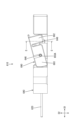
- FIG. 1 is a perspective view of an electronic component unit according to a first embodiment, illustrating a state in which the electronic component unit is connected to an electric wire.
- FIG. 2 is a plan view of the electronic component unit connected to the electric wire according to the first embodiment.
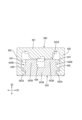
- FIG. 3 is a cross-sectional view taken along line AA of FIG.
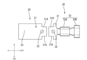
- FIG. 4 is a plan view of the first terminal and the second terminal according to the first embodiment.
- FIG. 5 is a plan view of the intermediate molded body according to the first embodiment.
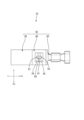
- FIG. 6 is a plan view of the electronic component unit according to the first embodiment.
- FIG. 7 is a perspective view of a wiring module including an electronic component unit according to the first embodiment.
- FIG. 8 is a perspective view of an electronic component unit according to the second embodiment, illustrating a state in which the electronic component unit is connected to an electric wire.
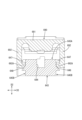
- FIG. 9 is a cross-sectional view of an electronic component unit according to the second embodiment, and corresponds to FIG. 3 of the first embodiment.
- FIG. 10 is a perspective view of an electronic component unit according to the third embodiment, illustrating a state in which the electronic component unit is connected to an electric wire.
- FIG. 11 is a cross-sectional view of an electronic component unit according to the third embodiment, and corresponds to FIG. 3 of the first embodiment.
- FIG. 12 is a cross-sectional view of an electronic component unit according to the fourth embodiment, and corresponds to FIG. 3 of the first embodiment.
- FIG. 13 is a perspective view of an electronic component unit according to the fifth embodiment, illustrating a state in which the electronic component unit is connected to an electric wire.
- FIG. 14 is a plan view of an electronic component unit according to the sixth embodiment, showing a state in which the electronic component unit is connected to an electric wire.
- FIG. 15 is a cross-sectional view taken along line BB of FIG.
- FIG. 16 is a perspective view of an electronic component unit according to the seventh embodiment, illustrating a state in which the electronic component unit is connected to an electric wire.
- FIG. 17 is a plan view of an electronic component unit connected to an electric wire according to the seventh embodiment.
- FIG. 18 is a cross-sectional view taken along line CC of FIG. FIG.
- FIG. 19 is a view showing a state in which the third terminal is inserted into the cavity, taken along the CC cross section of FIG. 20 is a cross-sectional view taken along the line CC of FIG. 17, showing a state in which the third terminal is inserted into the cavity and the retainer is in the provisionally retained position.
- FIG. 21 is a side view of an electronic component unit connected to an electric wire according to the seventh embodiment.
- FIG. 22 is a cross-sectional view taken along line DD of FIG. 21, and in FIG. 22, the second terminal, the third terminal, and the electric wires are omitted.
- FIG. 23 is a side view of the electronic component unit excluding the third terminal according to the seventh embodiment, showing a state in which the retainer is in the provisionally locked position.
- FIG. 24 is a cross-sectional view taken along line E--E of FIG.
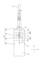
- FIG. 25 is a plan view of a first terminal, a second terminal, and a resin portion according to the seventh embodiment.
- 26 is a cross-sectional perspective view taken along the line FF in FIG. 25.
- FIG. FIG. 27 is a cross-sectional view taken along line GG of FIG.
- FIG. 28 is a plan view of a first terminal and a second terminal according to the seventh embodiment.
- FIG. 29 is a perspective view of an electronic component unit according to a modified example of the first embodiment, illustrating a state in which the electronic component unit is connected to an electric wire.
- FIG. 30 is a perspective view of an electronic component unit according to another embodiment, showing a state in which the electronic component unit is connected to a flexible substrate.
- the electronic component unit of the present disclosure comprises a first terminal electrically connected to a mating member, a second terminal directly or indirectly electrically connected to a wiring member, a resin part covering a part of the first terminal and a part of the second terminal, and an electronic component, wherein the resin part maintains a distance between the first terminal and the second terminal, the first terminal comprises a first connection part exposed from the resin part, the second terminal comprises a second connection part exposed from the resin part, and the electronic component comprises a first electrode mounted on the first connection part and a second electrode mounted on the second connection part.
- the resin portion has a peripheral wall portion that has a portion that protrudes beyond the first connection portion and the second connection portion and is disposed around the electronic component.
- the surrounding wall can protect the electronic components.
- the peripheral wall portion surrounds the first connection portion and the second connection portion.
- the peripheral wall portion can prevent foreign matter from coming into contact with the electronic component, thereby preventing stress from occurring at the connection portion between the first connection portion and the first electrode, and at the connection portion between the second connection portion and the second electrode.
- any one of the electronic component units [1] to [3] above further includes a cover member that covers the electronic component.
- the cover member can prevent condensation water and the like from adhering to the electronic components. This can prevent the first electrode and the second electrode from being short-circuited through condensation water and the like.
- any one of the electronic component units [1] to [4] above further comprises a third terminal to which the wiring member is connected, the second terminal comprises a first terminal connection portion connected to the third terminal, and the third terminal comprises a second terminal connection portion connected to the first terminal connection portion by fitting.
- This configuration makes it easier to connect the wiring member to the second terminal.
- the electronic component unit of [5] above further includes a retainer that is assembled to the resin portion and holds the third terminal.
- the third terminal can be held against the resin part, making it easier to determine the position of the third terminal relative to the resin part.
- the first terminal or the second terminal has a notch recessed from the outer edge, and the notch defines the first connection portion or the second connection portion.
- the notch defines the first connection portion or the second connection portion, so that the size of the first connection portion or the second connection portion can be appropriately adjusted, and heat dissipation from the first connection portion or the second connection portion can be controlled when mounting an electronic component.
- a groove is formed in the resin part, the groove being recessed toward the first connection part and the second connection part, the inner surface constituting the groove is continuous with the first connection part and the second connection part, and a part of the groove is disposed inside the notch.
- the plate thickness of the first terminal at the first connection portion is different from the plate thickness of the second terminal at the second connection portion, and that the first connection portion and the second connection portion are disposed at the same height.
- the first connection part and the second connection part are positioned at the same height, making it easy to mount electronic components.
- the manufacturing method of the electronic component unit disclosed herein includes a terminal forming process for forming a first terminal and a second terminal, a resin part forming process for forming a resin part by insert molding that covers a part of the first terminal and a part of the second terminal, exposing the outer surface of the first terminal as a first connection part and exposing the outer surface of the second terminal as a second connection part, and a mounting process for mounting the first electrode of an electronic component having a first electrode and a second electrode to the first connection part and mounting the second electrode to the second connection part.
- the electronic component can be easily included in the electronic component unit in the mounting process. Furthermore, even if the mating members to which the first terminal and the second terminal are respectively connected are changed, there are cases in which it is not necessary to redesign the electronic component unit, thereby reducing the manufacturing cost of the electronic component unit.
- first direction D1 and the second direction D2 are mutually perpendicular
- first direction D1 and the third direction D3 are mutually perpendicular
- second direction D2 and the third direction D3 are mutually perpendicular.
- an electronic component unit 10 of this embodiment includes a first terminal 20, a second terminal 30, a resin part 40, and an electronic component 50. Note that, for multiple identical members, reference numerals may be assigned to only some of the members, and the reference numerals of the other members may be omitted.
- the first terminal 20 is made of a conductive metal.
- conductive metals include aluminum and copper alloys.
- surface treatments of conductive metals include nickel plating and tin plating.
- the first terminal may be a first terminal in which nickel plating is formed on the surface of aluminum, a first terminal in which tin plating is formed on the surface of aluminum, or a first terminal in which tin plating is formed on the surface of copper alloy.
- the first terminal 20 has a plate-shaped portion 21 having a rectangular plate shape and a through hole 22 penetrating the plate-shaped portion 21.
- the through hole 22 is disposed at a position close to the end in the extension direction of the plate-shaped portion 21.
- the plate-shaped portion 21 has two recesses 21A at both ends in the width direction of the plate-shaped portion 21 (direction perpendicular to both the extension direction and the plate thickness direction of the plate-shaped portion 21).
- the recesses 21A are formed by recessing from the edge in the width direction of the plate-shaped portion 21.
- the plate-shaped portion 21 includes a mating member connection portion 23 that is electrically connected to a mating member.
- the mating member is, for example, a bus bar 60 (see FIG. 7).
- the mating member connecting portion 23 and the mating member are connected by, for example, welding or soldering.
- the second terminal 30 is made of a conductive metal.
- the metal constituting the second terminal 30 may be different from the metal constituting the first terminal 20.
- An example of the conductive metal is a copper alloy.
- an example of the surface treatment of the conductive metal is tin plating.
- the second terminal may be a copper alloy having a surface on which tin plating is formed.
- the second terminal 30 includes a plate-shaped portion 31 having a rectangular plate shape, a through hole 32 penetrating the plate-shaped portion 31, and a barrel portion 33.
- the barrel portion 33 is formed in a continuous manner with the plate-shaped portion 31 in the extension direction of the second terminal 30.
- the plate-shaped portion 31 has two recesses 31A at both ends in the width direction of the second terminal 30 (the direction perpendicular to both the extension direction of the second terminal 30 and the plate thickness direction of the plate-shaped portion 31).
- the recesses 31A are formed by recessing from the edge in the width direction of the second terminal 30.
- the barrel portion 33 includes a core wire crimping portion 33A and an insulating coating crimping portion 33B (an example of a fixing portion).
- the core wire crimping portion 33A is disposed between the plate-shaped portion 31 and the insulating coating crimping portion 33B in the extension direction of the second terminal 30.
- the core wire crimping portion 33A is crimped to the core wire of the electric wire 70 (an example of a wiring member).
- the second terminal 30 is electrically connected to the electric wire 70 by the core wire crimping portion 33A.
- the insulating coating crimping portion 33B is crimped to the insulating coating of the electric wire 70.
- the insulating coating crimping portion 33B can fix the electric wire 70 to the second terminal 30. For example, when a tensile stress is applied to the electric wire 70, the insulating coating crimping portion 33B suppresses the transmission of this tensile stress to the core wire crimping portion 33A. This makes it easier to maintain the electrical connection between the electric wire 70 and the second terminal 30.
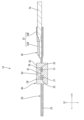
- the resin part 40 is made of an insulating synthetic resin. As shown in Figs. 1 to 3, the resin part 40 is disposed between the first terminal 20 and the second terminal 30, and covers a part of the first terminal 20 and a part of the second terminal 30. The resin part 40 is formed integrally with the first terminal 20 and the second terminal 30 by insert molding, as described later. As shown in Figs. 2 and 3, during insert molding, the molten resin, which is the raw material of the resin part 40, is filled into the through holes 22, 32 and the recesses 21A, 31A, so that the first terminal 20 and the second terminal 30 are held relative to the resin part 40. The resin part 40 positions the first terminal 20 and the second terminal 30 so as not to directly contact each other.
- the first terminal 20 and the second terminal 30 are disposed apart from each other in the first direction D1.
- the first terminal 20 is disposed so that the extension direction of the plate-shaped part 21 of the first terminal 20 is the first direction D1.
- the second terminals 30 are arranged such that the extension direction of the second terminals 30 is the first direction D1.
- the resin part 40 is formed to have a mounting surface 41.
- the mounting surface 41 is located between the first terminal 20 and the second terminal 30.
- the mounting surface 41 is a surface on which the electronic component 50 is mounted.
- the mounting surface 41 is perpendicular to a second direction D2 (hereinafter, described as the up-down direction).
- the second direction D2 coincides with the plate thickness direction of the plate-like parts 21, 31.
- the first connection portion 24 is exposed from the resin portion 40 next to the mounting surface 41.
- the first connection portion 24 is disposed at an end of the first terminal 20 closer to the second terminal 30 in the first direction D1.
- the first connection portion 24 is disposed flush with the mounting surface 41.
- the first connection portion 24 is parallel to the mounting surface 41 and disposed at the same position as the mounting surface 41 in the second direction D2.
- the first connection portion 24 is continuous with the mounting surface 41 in the first direction D1.
- flush means a state in which two parallel surfaces are smoothly connected without any steps, but in this specification, in addition to a state in which they are flush, it is also intended to include a state that is recognized as being substantially flush.
- a state recognized as being substantially flush means, for example, a state in which a minute step appears between the mounting surface 41 and the first connection portion 24 due to the effects of manufacturing tolerances, thermal expansion, etc., or a state in which the mounting surface 41 and the first connection portion 24 slightly intersect and are not strictly parallel to each other.
- the second connection portion 34 which is a part of the outer surface of the plate-shaped portion 31, is exposed from the mounting surface 41.
- the second connection portion 34 is exposed from the resin portion 40 next to the mounting surface 41.
- the second connection portion 34 is disposed at an end of the second terminal 30 closer to the first terminal 20 in the first direction D1.
- the second connection portion 34 is disposed flush with the mounting surface 41.
- the plate thickness of the plate-shaped portion 31 in the second connection portion 34 is different from the plate thickness of the plate-shaped portion 21 in the first connection portion 24, but the plate thickness of the plate-shaped portion 31 in the second connection portion 34 and the plate thickness of the plate-shaped portion 21 in the first connection portion 24 may be the same.
- the plate thickness of the plate-shaped portion 31 in the second connection portion 34 of the present disclosure is smaller than the plate thickness of the plate-shaped portion 21 in the first connection portion 24. Therefore, even if the plate-like portions 21, 31 have different plate thicknesses, the first connecting portion 24 and the second connecting portion 34 are disposed at the same height, so that the electronic component 50 can be easily mounted.
- the resin part 40 includes a peripheral wall part 42 that protrudes from the first connection part 24 and the second connection part 34.
- the peripheral wall part 42 protrudes, for example, along a direction perpendicular to the first connection part 24 and the second connection part 34.
- the peripheral wall part 42 also extends, for example, from the mounting surface 41 to one side (upward) in the second direction D2.
- the peripheral wall part 42 is disposed so as to surround the electronic component 50 in a direction perpendicular to the second direction D2.
- the peripheral wall part 42 is disposed so as not to contact the electronic component 50. As shown in FIG.
- the height of the peripheral wall part 42 from the mounting surface 41 (the dimension in the second direction D2) is greater than the height of the electronic component 50.
- the peripheral wall part 42 has four inner walls that form a square shape when viewed from the second direction D2.
- the length of the inner wall extending in the first direction D1 is approximately the same as the length of the inner wall extending in the third direction D3.
- the electronic component 50 includes a first electrode 51 and a second electrode 52.
- the first electrode 51 and the second electrode 52 are electrically insulated from each other.
- the electronic component 50 is placed on a placement surface 41.
- the first electrode 51 is disposed on the first connection portion 24, and the second electrode 52 is disposed on the second connection portion 34.
- the first electrode 51 and the first connection portion 24 are connected by soldering.
- the second electrode 52 and the second connection portion 34 are connected by soldering. That is, the electronic component 50 is mounted on an intermediate molded body 43 (see FIG. 5) that is composed of the first terminal 20, the second terminal 30, and the resin portion 40. Therefore, the electronic component 50 can be easily incorporated into the electronic component unit 10 through the mounting process (see FIG. 6).
- the electronic component unit 10 constitutes a member for mounting the electronic component 50 without using a flexible printed circuit (FPC). That is, the first terminal 20, the second terminal 30, and the resin part 40 form the first connection part 24 and the second connection part 34 on which the electronic component 50 can be mounted. This makes it easy to reduce the manufacturing cost of the electronic component unit 10.
- FPC flexible printed circuit
- the electronic component unit 10 of the present embodiment can be used in an electric storage module mounted on a vehicle such as an electric vehicle or a hybrid vehicle.
- the electric storage module includes a plurality of electric storage elements (not shown) and a wiring module 1 attached to the plurality of electric storage elements.
- the wiring module 1 includes the electronic component unit 10, a bus bar 60 connected to the mating member connection portion 23 of the first terminal 20, and an electric wire 70 connected to the barrel portion 33 of the second terminal 30.
- the bus bar 60 is connected to the electrode terminals of the plurality of electric storage elements.
- the electric wire 70 is connected to an ECU (Electronic Control Unit) or the like via a connector (not shown).
- the electric wire 70 functions as a voltage detection line.
- the wiring module 1 including the electronic component unit 10 has an electric wire 70 instead of an FPC as a voltage detection line. Therefore, the wiring module 1 can be manufactured at a lower cost compared to a wiring module in which an FPC is used as a voltage detection line.
- insert molding of the resin part 40 is performed using a part of the first terminal 20 and a part of the second terminal 30 as insert parts (resin part forming process).
- the first terminal 20 and the second terminal 30 are placed in a mold, and the mold is filled with molten resin, which is the raw material of the resin part 40.
- the first terminal 20 and the second terminal 30 are arranged so that they do not come into direct contact with each other.
- the first terminal 20 and the second terminal 30 are appropriately positioned in the mold so that the first connection part 24 and the second connection part 34 adjacent to the mounting surface 41 are exposed from the resin part 40, and the first connection part 24 and the second connection part 34 are flush with the mounting surface 41.
- the mold is removed, and an intermediate molded body 43 is obtained (see FIG. 5).
- the electronic component 50 is placed on the mounting surface 41 of the intermediate molded body 43, and the first electrode 51 is mounted to the first connection portion 24 and the second electrode 52 is mounted to the second connection portion 34 (mounting process, see Figure 6). This completes the manufacturing of the electronic component unit 10.
- the electronic component unit 10 of the present disclosure comprises a first terminal 20 electrically connected to a mating member (bus bar 60), a second terminal 30 directly or indirectly electrically connected to a wiring member (electric wire 70), a resin part 40 covering a part of the first terminal 20 and a part of the second terminal 30, and an electronic component 50, wherein the resin part 40 maintains the distance between the first terminal 20 and the second terminal 30, the first terminal 20 comprises a first connection part 24 exposed from the resin part 40, the second terminal 30 comprises a second connection part 34 exposed from the resin part 40, and the electronic component 50 comprises a first electrode 51 mounted on the first connection part 24 and a second electrode 52 mounted on the second connection part 34.
- the electronic component 50 can be easily included in the electronic component unit 10 by mounting. Furthermore, even if the mating member or wiring member is changed, there may be cases where the electronic component unit 10 does not need to be redesigned, so the manufacturing cost of the electronic component unit 10 can be reduced. Furthermore, it is expected that a need to change the material of the first terminal 20 to a dissimilar metal such as copper or aluminum will arise due to a change in the material of the mating member (bus bar 60). In such cases, by using the electronic component unit 10, the material of the first terminal 20 can be appropriately changed to a dissimilar metal regardless of the material of the second terminal 30.
- the resin part 40 has a peripheral wall part 42 that has a portion that protrudes beyond the first connection part 24 and the second connection part 34 and is disposed around the electronic component 50.
- the electronic components 50 can be protected by the peripheral wall portion 42.
- peripheral wall portion 42 surrounds the first connection portion 24 and the second connection portion 34.
- the peripheral wall 42 can prevent foreign matter from coming into contact with the electronic component 50, thereby preventing stress from occurring at the connection between the first connection 24 and the first electrode 51, and at the connection between the second connection 34 and the second electrode 52.
- the plate thickness of the plate-shaped portion 21 at the first connection portion 24 is different from the plate thickness of the plate-shaped portion 31 at the second connection portion 34, and the first connection portion 24 and the second connection portion 34 are disposed at the same height.
- the first connection portion 24 and the second connection portion 34 are positioned at the same height, making it easy to mount the electronic component 50.
- the manufacturing method of the electronic component unit 10 of the present disclosure includes a terminal forming process for forming the first terminal 20 and the second terminal 30, a resin part forming process for forming the resin part 40 by insert molding, the resin part 40 covering a part of the first terminal 20 and a part of the second terminal 30, exposing the outer surface of the first terminal 20 as the first connection part 24 and exposing the outer surface of the second terminal 30 as the second connection part 34, and a mounting process for mounting the first electrode 51 of the electronic component 50 having a first electrode 51 and a second electrode 52 to the first connection part 24 and the second electrode 52 to the second connection part 34.
- the resin part 40 that exposes the first connection part 24 and the second connection part 34 is formed in the resin part formation process, so that the electronic component 50 can be easily included in the electronic component unit 10 in the mounting process. Furthermore, even if the mating members to which the first terminal 20 and the second terminal 30 are respectively connected are changed, there are cases where it is not necessary to redesign the electronic component unit 10, so the manufacturing cost of the electronic component unit 10 can be reduced.
- An electronic component unit 110 according to the second embodiment is configured similarly to the first embodiment except that it further includes a lid portion 144 (an example of a cover member), and therefore descriptions of the same members and effects as those of the first embodiment will be omitted.
- the lid portion 144 is made of insulating synthetic resin, insulating tape, or the like. As shown in Fig. 9, the lid portion 144 is attached to the upper end surface of the peripheral wall portion 42, and closes the opening 42A formed by the peripheral wall portion 42. The lid portion 144 and the electronic component 50 are disposed with a space between them.
- the electronic component unit 110 of the second embodiment can be manufactured by attaching the lid portion 144 to the electronic component unit 10 of the first embodiment.
- the lid portion 144 can prevent water droplets from entering the opening 42A of the peripheral wall portion 42. Therefore, after the electronic component 50 melts, it is possible to prevent electrical continuity between the first connection portion 24 and the second connection portion 34 through the water droplets.
- An electronic component unit 210 according to the third embodiment is configured similarly to the first embodiment except that it further includes a sealing portion 245 (an example of a cover member), and therefore descriptions of the same members and effects as those of the first embodiment will be omitted.
- the sealing portion 245 is made of a curable insulating resin.
- the sealing portion 245 may be made of a resin different from the synthetic resin constituting the resin portion 40.
- the sealing portion 245 may be transparent.
- the sealing portion 245 of the third embodiment is, for example, a potting agent. As shown in FIG. 11, the sealing portion 245 is arranged so as to fill the space in the opening 42A of the peripheral wall portion 42.
- the sealing portion 245 is in close contact with the outer surface of the electronic component 50, the first connecting portion 24, the second connecting portion 34, and the mounting surface 41.
- the sealing portion 245 is formed by filling the opening 42A with liquid insulating resin before hardening after the mounting process and hardening the insulating resin.
- a bottomed recess is formed on the inside of the peripheral wall portion 42 by the inner circumferential surface of the peripheral wall portion 42, a surface of the portion of the resin portion 40 between the first terminal 20 and the second terminal 30 that is exposed to the inside of the peripheral wall portion 42, the surface of the first terminal 20 that is exposed to the inside of the peripheral wall portion 42, and the surface of the second terminal 30 that is exposed to the inside of the peripheral wall portion 42. Therefore, by arranging the molten sealing portion 245 in this recess, the electronic component 50, the connection portion between the first connection portion 24 and the first electrode 51, and the connection portion between the second connection portion 34 and the second electrode 52 can be easily covered by the sealing portion 245.
- a through hole 246 may be formed in the resin part 40.
- This through hole 246 penetrates the mounting surface 41 and the lower surface of the resin part 40.
- the through hole 246 exposes a part of the outer surface of the electronic component 50, which is different from the first electrode 51 and the second electrode 52, to the outside. In other words, the entire outer surface of the electronic component 50 is not covered by the sealing part 245 and the resin part 40.
- the first electrode 51 and the second electrode 52 are not exposed to the outside through the through hole 246.
- the through hole 246 may be formed, for example, in the resin part forming process or after the resin part forming process.
- the sealing portion 245 can prevent water droplets from entering the opening 42A of the peripheral wall portion 42. Therefore, after the electronic component 50 melts, it is possible to prevent electrical continuity between the first connection portion 24 and the second connection portion 34 through the water droplets.
- An electronic component unit 310 according to the fourth embodiment is configured substantially similarly to the third embodiment, except for the configuration of a sealing portion 345 (an example of a cover member), and therefore descriptions of the same members and effects as those of the first and third embodiments will be omitted.
- the sealing portion 345 in the fourth embodiment is, for example, a moisture-proof coating agent.
- the sealing portion 345 is in close contact with the outer surface of the electronic component 50, the first connecting portion 24, the second connecting portion 34, and the mounting surface 41 within the opening 42A of the peripheral wall portion 42.
- the sealing portion 345 does not have to fill the entire space within the opening 42A.
- An electronic component unit 410 according to the fifth embodiment is configured substantially similarly to the first embodiment except for the configuration of the second terminal 430, and therefore descriptions of the same members and effects as those of the first embodiment will be omitted.
- the second terminal 430 includes a plate-shaped portion 31, an electric wire connection portion 434, and an electric wire pressing portion 435 (an example of a fixing portion).
- the electric wire connection portion 434 is a plate-shaped member extending in the first direction D1 from the plate-shaped portion 31.
- the electric wire connection portion 434 is connected to the core wire of the electric wire 70 by soldering.
- the electric wire pressing portion 435 is disposed on the opposite side of the electric wire connection portion 434 from the plate-shaped portion 31.
- the electric wire pressing portion 435 includes a base portion 435A formed continuously from the electric wire connection portion 434 in the first direction D1, and an extension portion 435B extending in a cantilever shape from the base portion 435A in the third direction D3 (the width direction of the second terminal 430).
- the insulating coating of the electric wire 70 is clamped by the base portion 435A and the extension portion 435B bent so as to approach the base portion 435A. This allows the electric wire 70 to be fixed to the second terminal 430.
- the second terminal 430 does not necessarily have to include the electric wire pressing portion 435.
- FIG. 14 A sixth embodiment of the present disclosure will be described with reference to Fig. 14 and Fig. 15.
- An electronic component unit 510 according to the sixth embodiment is configured substantially similarly to the first embodiment, except that the peripheral wall portion 42 is not provided, and the configurations of the plate-shaped portions 521 and 531 are not provided. Therefore, a description of the same members and effects as those of the first embodiment will be omitted.
- the electronic component unit 510 includes a first terminal 520, a second terminal 530, a resin part 540, and an electronic component 50. As shown in FIG. 15, the resin part 540 does not have a peripheral wall part 42. The upper surface of the resin part 540 serves as the mounting surface 41.
- the plate-like portion 521 of the first terminal 520 includes a first plate portion 521A, a second plate portion 521B, and a third plate portion 521C.
- the second plate portion 521B and the third plate portion 521C are formed narrower than the first plate portion 521A (see FIG. 14).
- the first plate portion 521A is a plate-like member that is connected to the mating member connection portion 23 in the first direction D1.
- the second plate portion 521B extends upward from the end of the first plate portion 521A opposite the mating member connection portion 23 in the first direction D1.
- the third plate portion 521C extends in the first direction D1 from the upper end of the second plate portion 521B.
- the third plate portion 521C and the first plate portion 521A extend in opposite directions to each other in the first direction D1 relative to the second plate portion 521B.
- the upper surface of the third plate portion 521C is the first connection portion 24.
- the plate-shaped portion 531 of the second terminal 530 includes a first plate portion 531A, a second plate portion 531B, and a third plate portion 531C.
- the second plate portion 531B and the third plate portion 531C are formed narrower than the first plate portion 531A (see FIG. 14).
- the first plate portion 531A is a portion that is connected to the barrel portion 33 in the first direction D1.
- the second plate portion 531B extends upward from the end of the first plate portion 531A opposite the barrel portion 33 in the first direction D1.
- the third plate portion 531C extends in the first direction D1 from the upper end of the second plate portion 531B.
- the third plate portion 531C and the first plate portion 531A extend in opposite directions to each other in the first direction D1 relative to the second plate portion 531B.
- the upper surface of the third plate portion 531C is the second connection portion 34.
- the electronic component unit 610 according to the seventh embodiment further includes a third terminal 680, and the second terminal 630 and the electric wire 70 are connected via the third terminal 680.
- the same members and effects as those of the first embodiment may be omitted.
- the electronic component unit 610 includes a first terminal 620, a second terminal 630, a resin part 640, and an electronic component 50. As shown in Fig. 18, the electronic component unit 610 includes a third terminal 680 disposed inside the resin part 640. The third terminal 680 is connected to the electric wire 70.
- the first terminal 620 has a plate-shaped portion 21, a through hole 22, two recesses 21A, a mating member connection portion 23, and a first connection portion 24, similar to the first terminal 20 of the first embodiment.
- the first terminal 620 also has a notch 625 as a configuration different from the first terminal 20 of the first embodiment.
- the notch 625 is formed as a pair by being recessed from an outer edge portion on one side in the extension direction of the first terminal 620.
- the first connection portion 24 is defined by the notch 625. In other words, the first connection portion 24 and the notch 625 are adjacent to each other in the width direction of the first terminal 620.
- the notch 625 appropriately sets the area of the first connection portion 24 in a plan view.
- the notch 625 is not provided, when the first electrode 51 of the electronic component 50 and the first connection portion 24 are connected by soldering, the amount of heat transferred to the first terminal 620 may be large. However, in this embodiment, the size of the first connection portion 24 is appropriately adjusted using the notch 625, so that the amount of heat transferred to the first terminal 620 can be appropriately controlled.
- the second terminal 630 has a plate-shaped portion 31, a through hole 32, two recesses 31A, and a second connection portion 34, similar to the second terminal 30 of the first embodiment.
- the plate-shaped portion 31 has two recesses 31A at both ends in the width direction of the second terminal 30 (a direction perpendicular to both the extension direction of the second terminal 30 and the plate thickness direction of the plate-shaped portion 31).
- the recesses 31A are formed by being recessed from the edge of the width direction of the second terminal 30.
- the second terminal 630 also includes a tab portion 633 (an example of a first terminal connection portion).
- the tab portion 633 is formed in a continuous manner with the plate-shaped portion 31 in the extension direction of the second terminal 630.
- the tab portion 633 is rod-shaped and extends from the edge of the plate-shaped portion 31 in the extension direction of the second terminal 630.
- the second terminal 630 is provided with a notch 635, similar to the first terminal 620.
- the notch 635 is formed as a pair by being recessed from the outer edge portion opposite the tab portion 633 in the extension direction of the second terminal 630.
- the second connection portion 34 is defined by the notch 635.
- the second connection portion 34 and the notch 635 are adjacent to each other in the width direction of the second terminal 630.
- the notch 635 appropriately sets the area of the second connection portion 34 in a plan view.
- the third terminal 680 is made of a conductive metal.
- the metal constituting the third terminal 680 may be different from the metal constituting the first terminal 620 and the metal constituting the second terminal 630.
- the third terminal 680 includes a connection tube portion 681 (an example of a second terminal connection portion) connected to the second terminal 630, and a barrel portion 682.
- the barrel portion 682 is formed to be continuous with the connection tube portion 681 in the extension direction of the third terminal 680.
- the barrel portion 682 includes a core wire crimping portion 682A that is crimped to the core wire of the electric wire 70, and an insulating coating crimping portion 682B that is crimped to the insulating coating of the electric wire 70.
- connection tube portion 681 includes a tube wall portion 683 having, for example, a rectangular tube shape, and an elastic contact piece 684 formed inside the tube wall portion 683.
- the tube wall portion 683 is open in the first direction D1.
- the elastic contact piece 684 extends from the inner surface of the tube wall portion 683 and is elastically deformable in a direction perpendicular to the first direction D1.
- the connection tube portion 681 also has a locking hole 683A formed penetrating the tube wall portion 683. As shown in FIG. 18 to FIG.
- the tab portion 633 of the second terminal 630 is inserted into the tube wall portion 683, and the elastic contact piece 684 comes into contact with the tab portion 633, thereby electrically connecting the third terminal 680 and the second terminal 630. That is, the connection tube portion 681 and the tab portion 633 are electrically connected by fitting. Therefore, the second terminal 630 and the electric wire 70 are electrically connected via the third terminal 680.
- the second terminal 630 is not directly connected to the electric wire 70, but is indirectly connected to the electric wire 70 via the third terminal 680. Therefore, when electrically connecting the electronic component unit 610 and the electric wire 70, for example, it is possible to prevent the connection portion between the electronic component 50 and the second terminal 630 from being damaged by stress or the like. This makes it easier to ensure the reliability of the electrical connection between the electronic component unit 610 and the electric wire 70.
- the resin part 640 covers a part of the first terminal 620 and a part of the second terminal 630.
- the resin part 640 is formed integrally with the first terminal 620 and the second terminal 630 by insert molding, as in the first embodiment.
- the first terminal 620 and the second terminal 630 are fixed to the resin part 640.
- the resin part 640 has an intermediate part 641 disposed between the first terminal 620 and the second terminal 630 in the first direction D1.
- the resin part 640 maintains the distance between the first terminal 620 and the second terminal 630.
- the resin part 640 exposes the first connection part 24, which is a part of the outer surface of the plate part 21, and the second connection part 34, which is a part of the outer surface of the plate part 31.
- the first connection part 24 and the second connection part 34 are disposed at a predetermined distance in the first direction D1 by the resin part 640. Further, the resin portion 640 exposes the mating member connecting portion 23 to the outside.
- one end face (upper) of the intermediate portion 641 in the second direction D2 is set as the reference surface 641A.
- the reference surface 641A is disposed flush with the first connection portion 24 (outer surface of the plate-shaped portion 21) and the second connection portion 34 (outer surface of the plate-shaped portion 31).
- the reference surface 641A is perpendicular to the second direction D2 (up-down direction).
- the second direction D2 coincides with the plate thickness direction of the plate-shaped portions 21, 31.
- the resin portion 640 may have a through hole 246, similar to the third embodiment.
- the through hole 246 penetrates the middle portion 641 in the second direction D2.
- the resin part 640 has a peripheral wall portion 42, similar to the first embodiment.
- the peripheral wall portion 42 extends from the reference surface 641A to one side (upward) in the second direction D2. That is, the peripheral wall portion 42 has a portion that protrudes upward beyond the first connection portion 24 and the second connection portion 34.
- the peripheral wall portion 42 is disposed around the electronic component 50.
- the peripheral wall portion 42 also surrounds the first connection portion 24 and the second connection portion 34 in a direction perpendicular to the second direction D2.
- the intermediate portion 641 has a groove 641B recessed from the reference surface 641A to the other side (downward) in the second direction D2.
- the groove 641B is recessed downward with respect to the first connecting portion 24 and the second connecting portion 34.
- the groove 641B is composed of a bottom surface BS that is approximately parallel to the reference surface 641A, a first inner surface S1 that connects the bottom surface BS and the first connecting portion 24, a second inner surface S2 that connects the bottom surface BS and the second connecting portion 34, and a third inner surface S3 that connects the bottom surface BS and the reference surface 641A.
- the groove 641B is adjacent to each of the first connecting portion 24 and the second connecting portion 34 when viewed from a direction (second direction D2) perpendicular to the first connecting portion 24 and the second connecting portion 34.
- the bottom surface BS faces the electronic component 50 in the second direction D2.
- a gap is provided between the bottom surface BS and the electronic component 50.
- a portion of the groove 641B is disposed inside the notches 625 and 635.
- the first side surface part SP1 a part of the side surface of the first terminal 620 continuing from the outer edge of the first connection part 24 (hereinafter, the first side surface part SP1) may be exposed from the resin part 640.
- the first connection part 24 and the first inner surface S1 may be connected via the first side surface part SP1.
- a part of the side surface of the second terminal 630 continuing from the outer edge of the second connection part 34 (hereinafter, the second side surface part) may be exposed from the resin part 640.
- the second connection part 34 and the second inner surface S2 may be connected via the second side surface part.
- the first connection portion 24 and the inner surface of the groove 641 may be directly connected.
- the second connection portion 34 and the inner surface of the groove 641 may be directly connected.
- the molten resin may move to the outer surface (top surface) of the first connection part 24 and the second connection part 34, and burrs may occur on the first connection part 24 and the second connection part 34. In such a case, the burrs may cause a poor electrical connection between the first connection part 24 and the first electrode 51 or between the second connection part 34 and the second electrode 52.
- the groove 641B is provided in the intermediate part 641, when the resin part 640 is formed, the molten resin is more likely to move into the groove 641B than to the top surface of the first connection part 24 and the second connection part 34. Therefore, it is possible to suppress the occurrence of burrs on the first connection part 24 and the second connection part 34.
- the resin part 640 has a housing part 643 formed continuously with the intermediate part 641 and the peripheral wall part 42.
- the housing part 643 extends on the opposite side of the first terminal 620 from the intermediate part 641.
- the housing part 643 has a cavity 644 in which the third terminal 680 is accommodated.
- the cavity 644 extends in the first direction D1 and opens to one side in the first direction D1 (the right side in the figure).
- the tab part 633 of the second terminal 630 and a part of the plate part 31 which is the base end part of the tab part 633 are arranged at the end of the cavity 644 on the other side in the first direction D1 (the left side in the figure).
- the housing portion 643 includes a bottom wall 643A (see FIG. 18), a pair of side walls 643B, and a ceiling wall 643C.
- the pair of side walls 643B extend from both ends of the bottom wall 643A in the third direction D3 to one side (upward) in the second direction D2.
- the ceiling wall 643C faces the bottom wall 643A in the second direction D2.
- the ceiling wall 643C connects one end (upper end) of the pair of side walls 643B in the second direction D2.
- the cavity 644 is an internal space defined by the bottom wall 643A, the pair of side walls 643B, and the ceiling wall 643C.
- a first communication hole 643C1 is provided in a portion of the ceiling wall 643C closer to the middle portion 641.
- the first communication hole 643C1 penetrates the ceiling wall 643C in the second direction D2 and communicates with the cavity 644.
- a second communication hole 643A1 is provided in the end of the bottom wall 643A closer to the middle portion 641.
- the second communication hole 643A1 penetrates the bottom wall 643A in the second direction D2 and communicates with the cavity 644.
- a mounting recess 645 for mounting a retainer 690 (described later) is formed in approximately two-thirds of the area on the other side (left side in the figure) of the housing portion 643 in the first direction D1.
- the mounting recess 645 has a first mounting recess 645A recessed from the outer surface of the ceiling wall 643C, and a second mounting recess 645B recessed from the outer surfaces of the pair of side walls 643B.
- the end of the first mounting recess 645A closer to the middle portion 641 extends to the peripheral wall portion 42.
- the first mounting recess 645A communicates with the first communication hole 643C1.
- the second mounting recess 645B is connected to the first mounting recess 645A.
- the housing portion 643 includes a shaft portion 646, a temporary locking portion 647, and a full locking portion 648 that protrude from the inner wall of the second mounting recess 645B in the third direction D3.
- the shaft portion 646 is generally cylindrical.
- the shaft portion 646 is disposed on a portion of the inner wall of the second mounting recess 645B closer to the middle portion 641 in the first direction D1.
- the temporary locking portion 647 and the full locking portion 648 are disposed on an end of the inner wall of the second mounting recess 645B opposite the middle portion 641 in the first direction D1.
- the temporary locking portion 647 and the full locking portion 648 are disposed close to each other.
- the temporary locking portion 647 is disposed on one side (the right side in the figure) of the full locking portion 648 in the first direction D1.
- the provisional locking portion 647 is disposed on one side (above) of the full locking portion 648 in the second direction D2.
- the electronic component unit 610 of this embodiment includes a retainer 690 that is assembled to the resin part 640.
- the retainer 690 is made of insulating synthetic resin.
- the retainer 690 is adapted to be assembled to the resin part 640 at a provisional locking position (see Fig. 23) and a full locking position (see Fig. 21).
- the retainer 690 is substantially gate-shaped when viewed from the first direction D1.
- the retainer 690 includes a main body part 691, a pair of lock pieces 692, and a pair of side walls 693.
- the pair of lock pieces 692 and the pair of side walls 693 extend from both ends of the main body part 691 in the third direction D3.
- the lock piece 692 is disposed on one side (the right side in the figure) of the side wall 693 in the first direction D1. 22, the main body 691 is adapted to be housed in the first mounting recess 645A.
- the pair of lock pieces 692 and the pair of side walls 693 are adapted to be housed in the second mounting recess 645B.
- the retainer 690 includes a lance 694 and a retaining portion 695.
- the lance 694 extends from the main body portion 691 to the other side (the left side in the figure) in the first direction D1 and also to the other side (downward) in the second direction D2.
- the lance 694 is elastically deformable with respect to the main body portion 691.
- the retaining portion 695 protrudes from the main body portion 691 to the other side (downward) in the second direction D2.
- the retaining portion 695 is generally block-shaped.
- the removal prevention portion 695 does not enter the cavity 644, and only the tip of the lance 694 enters the cavity 644 through the first communication hole 643C1.
- the third terminal 680 is allowed to be inserted from the opening on one side (the right side in the figure) of the cavity 644 in the first direction D1. This is because the removal prevention portion 695 is not positioned in a position that will interfere with the third terminal 680, and the lance 694 can elastically deform even if it interferes with the third terminal 680.
- the lance 694 and the retaining portion 695 are disposed in the cavity 644 through the first communication hole 643C1.
- the lance 694 engages with the inner wall of the locking hole 683A of the third terminal 680.
- the retaining portion 695 engages with the end of the connecting tube portion 681 on one side (right side in the figure) in the first direction D1. This allows the third terminal 680 to be held in the cavity 644. That is, the third terminal 680 can be held against the resin portion 640.
- the third terminal 680 abuts against the edge (see FIG.
- the retainer 690 has an insertion hole 693A that penetrates the side wall 693 in the third direction D3.
- the shaft portion 646 is inserted into the insertion hole 693A.
- the retainer 690 is rotatable about the shaft portion 646, and is movable between a provisional locking position and a full locking position.
- the retainer 690 has a locking protrusion 692A that protrudes from the tip of the lock piece 692 toward the inner wall of the second mounting recess 645B.
- the locking protrusion 692A is disposed between the temporary locking portion 647 and the full locking portion 648, thereby holding the retainer 690 in the temporary locking position.
- the locking protrusion 692A is disposed on the other side (lower) in the second direction D2 relative to the full locking portion 648, thereby holding the retainer 690 in the full locking position.
- the locking protrusion 692A engages with the full locking portion 648, thereby preventing the retainer 690 from rotating counterclockwise in FIG. 21 from the full locking position. Furthermore, the main body 691 and the inner wall of the first mounting recess 645A are engaged to prevent the retainer 690 from rotating clockwise in FIG. 21 from the main engagement position.
- the above is the configuration of the electronic component unit 610.
- An example of a manufacturing method for the electronic component unit 610 will be described below.
- the resin part 640 is integrally molded with the first terminal 620 and the second terminal 630 by insert molding (see FIG. 25 ).
- the first electrode 51 and the second electrode 52 of the electronic component 50 are mounted on the first connection part 24 and the second connection part 34, respectively.
- the retainer 690 is attached to the resin part 640, and the retainer 690 is placed in the temporary locking position. That is, the shaft part 646 is inserted into the insertion hole 693A, and the locking protrusion 692A is placed in the gap between the temporary locking part 647 and the full locking part 648.
- the third terminal 680 which has been previously formed from a metal plate and connected to the electric wire 70, is inserted (see FIG. 19).
- the lance 694 interferes with the connecting tube portion 681 and elastically deforms.
- the lance 694 elastically returns to its original position and enters the locking hole 683A (see FIG. 20).
- the retainer 690 When the third terminal 680 is placed in the correct position in the cavity 644, the retainer 690 is moved to the full locking position.
- the lock piece 692 When the retainer 690 is rotated clockwise in FIG. 23 from the provisional locking position, the lock piece 692 is elastically deformed, and the locking projection 692A passes over the full locking portion 648.
- the lock piece 692 moves to the other side (downward) in the second direction D2 relative to the full locking portion 648, the lock piece 692 elastically returns, and the retainer 690 reaches the full locking position (see FIG. 22).
- the lance 694 enters the depth of the locking hole 683A, and the lance 694 and the inner wall of the locking hole 683A are arranged to be able to engage with each other (see FIG.
- the removal prevention portion 695 is arranged on one side (the right side in the figure) in the first direction D1 relative to the connection tube portion 681, and is arranged to be able to engage with the connection tube portion 681. This holds the third terminal 680 in the cavity 644. This completes the manufacturing of the electronic component unit 610.
- the electronic component unit 610 according to the seventh embodiment further includes a third terminal 680 to which a wiring member (electric wire 70) is connected, the second terminal 630 includes a first terminal connection portion (tab portion 633) connected to the third terminal 680, and the third terminal 680 includes a second terminal connection portion (connection tube portion 681) connected by fitting to the first terminal connection portion.
- This configuration makes it easier to connect the wiring member to the second terminal 630.
- the electronic component unit 610 according to the seventh embodiment further includes a retainer 690 that is attached to the resin part 640 and holds the third terminal 680.
- the third terminal 680 can be held relative to the resin part 640, making it easier to determine the position of the third terminal 680 relative to the resin part 640.
- the first terminal 620 or the second terminal 630 has a notch 625, 635 recessed from the outer edge, and the notch 625, 635 defines the first connection portion 24 or the second connection portion 34.
- the first connection portion 24 or the second connection portion 34 is defined by the notches 625, 635, so that the size of the first connection portion 24 or the second connection portion 34 can be appropriately adjusted, and heat dissipation from the first connection portion 24 or the second connection portion 34 can be controlled when mounting the electronic component 50.
- a groove 641B is formed in the resin part 640, which is recessed toward the first connection part 24 and the second connection part 34, and the inner surfaces (first inner surface S1 and second inner surface S2) that form the groove 641B are continuous with the first connection part 24 and the second connection part 34, and a part of the groove 641B is disposed inside the notches 625, 635.
- the shapes of the first terminal, the second terminal, and the resin part, and their relative arrangement are not limited to those described in the above embodiments 1 to 7, and may be modified as appropriate within the scope of the objectives of this disclosure.
- the end faces of the first terminal 20 and the second terminal 30 in the third direction D3 are substantially flush with the end face of the resin part 40 in the third direction D3 (see FIG. 1), but the end faces of the first terminal and the second terminal in the third direction D3 do not have to be substantially flush with the end face of the resin part in the third direction D3.
- an aspect may be adopted in which the resin part 40 covers the end faces of the first terminal 20 and the second terminal 30 in the third direction D3, as shown in FIG. 29.
- the mating member was a bus bar 60, but the mating member does not have to be a bus bar and may be, for example, an electrode terminal.
- the wiring member is an electric wire 70, but the wiring member does not have to be an electric wire.
- the electronic component unit 710 may include a second terminal 730 connected to a flexible substrate 770, which is an example of a wiring member.
- the flexible substrate 770 is, for example, a flexible printed circuit board or a flexible flat cable.
- the flexible substrate 770 and the second terminal 730 may be connected by, for example, soldering.
- the mounting surface 41 of the resin part 40 is flush with the first connection part 24 of the first terminal 20 and the second connection part 34 of the second terminal 30, but the mounting surface may be formed with a step relative to the first connection part and the second connection part.
- the resin part 40 has a mounting surface 41 on which the electronic component 50 is placed, but the resin part does not have to have a mounting surface. In other words, the resin part does not have to have a surface that contacts the electronic component, and it is sufficient that the first electrode and the second electrode of the electronic component are connected to the first connection part of the first terminal and the second connection part of the second terminal, respectively.
- the electronic component unit 610 includes a retainer 690 that is attached to the resin portion 640, but the electronic component unit does not need to include a retainer. If no retainer is provided, the housing portion may be provided with a retaining portion for holding the third terminal within the cavity.
- the tab portion 633 is exemplified as the first terminal connection portion
- the connection tube portion 681 is exemplified as the second terminal connection portion
- the first terminal connection portion may be the connection tube portion
- the second terminal connection portion may be the tab portion
- the shape of the retainer 690 in the seventh embodiment is an example, and the shape of the retainer may be changed as desired as long as it has the function of fixing the third terminal to the resin part.
- the retainer 690 is held at a provisional locking position and a full locking position relative to the resin part 640, but it is also possible to set only the full locking position and omit the provisional locking position.
- the retainer may move linearly rather than rotating relative to the resin part.
- Wiring module 10 Electronic component unit 20: First terminal 21: Plate-shaped portion 21A: Recess 22: Through hole 23: Mating member connection portion 24: First connection portion 30: Second terminal 31: Plate-shaped portion 31A: Recess 32: Through hole 33: Barrel portion 33A: Core wire crimping portion 33B: Insulation coating crimping portion (fixing portion) 34: Second connection portion 40: Resin portion 41: Mounting surface 42: Peripheral wall portion 43: Intermediate molded body 50: Electronic component 51: First electrode 52: Second electrode 60: Bus bar (mating member) 70: Electric wire (wiring member) 110: Electronic component unit 144: Lid portion (cover member) 210: Electronic component unit 245: Sealing portion (cover member) 246: Through hole 310: Electronic component unit 345: Sealing portion (cover member) 410: Electronic component unit 430: Second terminal 434: Electric wire connection portion 435: Electric wire pressing portion (fixing portion) 435A: Base portion 435B: Extension portion 510: Electronic component unit 520
Landscapes
- Chemical & Material Sciences (AREA)
- Chemical Kinetics & Catalysis (AREA)
- Electrochemistry (AREA)
- General Chemical & Material Sciences (AREA)
- Engineering & Computer Science (AREA)
- Manufacturing & Machinery (AREA)
- Connection Of Batteries Or Terminals (AREA)
- Details Of Connecting Devices For Male And Female Coupling (AREA)
- Manufacturing Of Electrical Connectors (AREA)
- Fuses (AREA)
- Connector Housings Or Holding Contact Members (AREA)
- Structures Or Materials For Encapsulating Or Coating Semiconductor Devices Or Solid State Devices (AREA)
- Switch Cases, Indication, And Locking (AREA)
Priority Applications (2)
| Application Number | Priority Date | Filing Date | Title |
|---|---|---|---|
| CN202480033161.2A CN121195325A (zh) | 2023-06-01 | 2024-06-03 | 电子部件单元及电子部件单元的制造方法 |
| JP2025524927A JPWO2024248160A1 (https=) | 2023-06-01 | 2024-06-03 |
Applications Claiming Priority (4)
| Application Number | Priority Date | Filing Date | Title |
|---|---|---|---|
| JP2023090832 | 2023-06-01 | ||
| JP2023-090832 | 2023-06-01 | ||
| JPPCT/JP2024/000420 | 2024-01-11 | ||
| PCT/JP2024/000420 WO2024247346A1 (ja) | 2023-06-01 | 2024-01-11 | ヒューズユニット及びヒューズユニットの製造方法 |
Publications (1)
| Publication Number | Publication Date |
|---|---|
| WO2024248160A1 true WO2024248160A1 (ja) | 2024-12-05 |
Family
ID=92909777
Family Applications (1)
| Application Number | Title | Priority Date | Filing Date |
|---|---|---|---|
| PCT/JP2024/020162 Ceased WO2024248160A1 (ja) | 2023-06-01 | 2024-06-03 | 電子部品ユニット及び電子部品ユニットの製造方法 |
Country Status (3)
| Country | Link |
|---|---|
| JP (6) | JP7561318B1 (https=) |
| CN (2) | CN121153096A (https=) |
| WO (1) | WO2024248160A1 (https=) |
Cited By (1)
| Publication number | Priority date | Publication date | Assignee | Title |
|---|---|---|---|---|
| CN119674471A (zh) * | 2025-02-20 | 2025-03-21 | 宁德时代新能源科技股份有限公司 | 电池装置及用电设备 |
Citations (11)
| Publication number | Priority date | Publication date | Assignee | Title |
|---|---|---|---|---|
| JPS5054860A (https=) * | 1974-09-05 | 1975-05-14 | ||
| JPH09139256A (ja) * | 1995-11-15 | 1997-05-27 | Harness Sogo Gijutsu Kenkyusho:Kk | ヒューズ内蔵型コネクタ及びその製造方法 |
| JPH11185885A (ja) * | 1997-12-24 | 1999-07-09 | Yazaki Corp | 過電流保護付ジョイントコネクタ |
| JP2000260534A (ja) * | 1999-03-10 | 2000-09-22 | Sumitomo Wiring Syst Ltd | 端子金具、及びコネクタ |
| JP2009070803A (ja) * | 2007-08-20 | 2009-04-02 | Uchihashi Estec Co Ltd | 抵抗付き温度ヒューズ及び電池保護回路板 |
| DE102009052353A1 (de) * | 2009-11-07 | 2011-05-12 | Volkswagen Ag | Kontaktstecker |
| JP2014013707A (ja) * | 2012-07-05 | 2014-01-23 | Auto Network Gijutsu Kenkyusho:Kk | 電気素子内蔵コネクタ |
| DE102015110593A1 (de) * | 2015-07-01 | 2017-01-05 | Lisa Dräxlmaier GmbH | Stecksicherungselement |
| JP2019032928A (ja) * | 2017-08-04 | 2019-02-28 | 矢崎総業株式会社 | 導体モジュール |
| WO2020194967A1 (ja) * | 2019-03-27 | 2020-10-01 | 三洋電機株式会社 | 過電流保護素子とバッテリーシステム |
| JP2022127478A (ja) * | 2021-02-19 | 2022-08-31 | デクセリアルズ株式会社 | 保護素子 |
Family Cites Families (5)
| Publication number | Priority date | Publication date | Assignee | Title |
|---|---|---|---|---|
| JPH08330007A (ja) * | 1995-05-29 | 1996-12-13 | Sato Seiki:Kk | 接続用の電気部品 |
| JP2001307610A (ja) * | 2000-04-17 | 2001-11-02 | Sanyo Electric Co Ltd | ヒューズの製造方法とこのヒューズを内蔵するパック電池 |
| JP2013118174A (ja) * | 2011-11-04 | 2013-06-13 | Jst Mfg Co Ltd | 防水コネクタ及びその製造方法 |
| JP6458996B2 (ja) | 2015-04-24 | 2019-01-30 | 株式会社オートネットワーク技術研究所 | 雄型コネクタ |
| CN209561113U (zh) * | 2019-04-12 | 2019-10-29 | 昆山万丰电子有限公司 | 一种贴片式热熔断复合型压敏电阻器组件 |
-
2024
- 2024-01-11 CN CN202480033556.2A patent/CN121153096A/zh active Pending
- 2024-01-11 JP JP2024520026A patent/JP7561318B1/ja active Active
- 2024-06-03 CN CN202480033161.2A patent/CN121195325A/zh active Pending
- 2024-06-03 WO PCT/JP2024/020162 patent/WO2024248160A1/ja not_active Ceased
- 2024-06-03 JP JP2025524927A patent/JPWO2024248160A1/ja active Pending
- 2024-08-06 JP JP2024129678A patent/JP7850379B2/ja active Active
- 2024-08-06 JP JP2024129677A patent/JP7803381B2/ja active Active
- 2024-08-06 JP JP2024129676A patent/JP7803380B2/ja active Active
- 2024-12-26 JP JP2024229793A patent/JP2025041905A/ja active Pending
Patent Citations (11)
| Publication number | Priority date | Publication date | Assignee | Title |
|---|---|---|---|---|
| JPS5054860A (https=) * | 1974-09-05 | 1975-05-14 | ||
| JPH09139256A (ja) * | 1995-11-15 | 1997-05-27 | Harness Sogo Gijutsu Kenkyusho:Kk | ヒューズ内蔵型コネクタ及びその製造方法 |
| JPH11185885A (ja) * | 1997-12-24 | 1999-07-09 | Yazaki Corp | 過電流保護付ジョイントコネクタ |
| JP2000260534A (ja) * | 1999-03-10 | 2000-09-22 | Sumitomo Wiring Syst Ltd | 端子金具、及びコネクタ |
| JP2009070803A (ja) * | 2007-08-20 | 2009-04-02 | Uchihashi Estec Co Ltd | 抵抗付き温度ヒューズ及び電池保護回路板 |
| DE102009052353A1 (de) * | 2009-11-07 | 2011-05-12 | Volkswagen Ag | Kontaktstecker |
| JP2014013707A (ja) * | 2012-07-05 | 2014-01-23 | Auto Network Gijutsu Kenkyusho:Kk | 電気素子内蔵コネクタ |
| DE102015110593A1 (de) * | 2015-07-01 | 2017-01-05 | Lisa Dräxlmaier GmbH | Stecksicherungselement |
| JP2019032928A (ja) * | 2017-08-04 | 2019-02-28 | 矢崎総業株式会社 | 導体モジュール |
| WO2020194967A1 (ja) * | 2019-03-27 | 2020-10-01 | 三洋電機株式会社 | 過電流保護素子とバッテリーシステム |
| JP2022127478A (ja) * | 2021-02-19 | 2022-08-31 | デクセリアルズ株式会社 | 保護素子 |
Cited By (1)
| Publication number | Priority date | Publication date | Assignee | Title |
|---|---|---|---|---|
| CN119674471A (zh) * | 2025-02-20 | 2025-03-21 | 宁德时代新能源科技股份有限公司 | 电池装置及用电设备 |
Also Published As
| Publication number | Publication date |
|---|---|
| JP7850379B2 (ja) | 2026-04-23 |
| JP2025041905A (ja) | 2025-03-26 |
| JP7803381B2 (ja) | 2026-01-21 |
| JP2024173927A (ja) | 2024-12-13 |
| JP2024173928A (ja) | 2024-12-13 |
| JP7561318B1 (ja) | 2024-10-04 |
| JP2024173846A (ja) | 2024-12-12 |
| CN121153096A (zh) | 2025-12-16 |
| CN121195325A (zh) | 2025-12-23 |
| JPWO2024247346A1 (https=) | 2024-12-05 |
| JPWO2024248160A1 (https=) | 2024-12-05 |
| JP7803380B2 (ja) | 2026-01-21 |
Similar Documents
| Publication | Publication Date | Title |
|---|---|---|
| US8342880B2 (en) | Electrical connector with elastically held terminals | |
| WO2024247346A1 (ja) | ヒューズユニット及びヒューズユニットの製造方法 | |
| US9305732B2 (en) | Electronic part and electronic control unit | |
| US20150077959A1 (en) | Connector device for a printed circuit board of a control device for a vehicle transmission, control system for a vehicle transmission and method for assembling a control system for a vehicle transmission | |
| US8366457B2 (en) | Wiring structure having a plurality of circuit boards with an insulating sleeve in a terminal insertion hole | |
| JP2017135799A (ja) | 電子部品ユニット、及び電気接続箱 | |
| CN112531379B (zh) | 电路单元、电气接线箱及电路单元的制造方法 | |
| JP7803381B2 (ja) | ヒューズユニット及びヒューズユニットの製造方法 | |
| US10464510B2 (en) | Power supply device and method for producing the same | |
| JP7648007B1 (ja) | 配線モジュール | |
| JP2026074365A (ja) | 配線モジュール | |
| WO2026014310A1 (ja) | 電子部品ユニット及び配線モジュール | |
| CN121219906A (zh) | 布线模块 | |
| WO2026014305A1 (ja) | 電子部品ユニット及び配線モジュール | |
| JP7512992B2 (ja) | コネクタ | |
| JP7560509B2 (ja) | バスバモジュール | |
| JP7757229B2 (ja) | ケースモールド型フィルムコンデンサ | |
| JP7755564B2 (ja) | 電気接続箱 | |
| JP2002216870A (ja) | 基板用コネクタ | |
| EP4654241A1 (en) | Fuse holder device for high-power electrical circuit | |
| JP2025001707A (ja) | 導電モジュール | |
| JP2025001708A (ja) | 導電モジュール | |
| US10468200B2 (en) | Power supply device | |
| JP2012005284A (ja) | 電気接続箱 |
Legal Events
| Date | Code | Title | Description |
|---|---|---|---|
| 121 | Ep: the epo has been informed by wipo that ep was designated in this application |
Ref document number: 24815639 Country of ref document: EP Kind code of ref document: A1 |
|
| ENP | Entry into the national phase |
Ref document number: 2025524927 Country of ref document: JP Kind code of ref document: A |
|
| WWE | Wipo information: entry into national phase |
Ref document number: 2025524927 Country of ref document: JP |
|
| NENP | Non-entry into the national phase |
Ref country code: DE |