WO2024241666A1 - 電磁波反射パネル、電磁波反射装置、及び電磁波反射フェンス - Google Patents
電磁波反射パネル、電磁波反射装置、及び電磁波反射フェンス Download PDFInfo
- Publication number
- WO2024241666A1 WO2024241666A1 PCT/JP2024/009354 JP2024009354W WO2024241666A1 WO 2024241666 A1 WO2024241666 A1 WO 2024241666A1 JP 2024009354 W JP2024009354 W JP 2024009354W WO 2024241666 A1 WO2024241666 A1 WO 2024241666A1
- Authority
- WO
- WIPO (PCT)
- Prior art keywords
- electromagnetic wave
- dielectric substrate
- wave reflecting
- layer
- film
- Prior art date
- Legal status (The legal status is an assumption and is not a legal conclusion. Google has not performed a legal analysis and makes no representation as to the accuracy of the status listed.)
- Ceased
Links
Images



Classifications
-
- B—PERFORMING OPERATIONS; TRANSPORTING
- B32—LAYERED PRODUCTS
- B32B—LAYERED PRODUCTS, i.e. PRODUCTS BUILT-UP OF STRATA OF FLAT OR NON-FLAT, e.g. CELLULAR OR HONEYCOMB, FORM
- B32B7/00—Layered products characterised by the relation between layers; Layered products characterised by the relative orientation of features between layers, or by the relative values of a measurable parameter between layers, i.e. products comprising layers having different physical, chemical or physicochemical properties; Layered products characterised by the interconnection of layers
- B32B7/02—Physical, chemical or physicochemical properties
- B32B7/025—Electric or magnetic properties
-
- E—FIXED CONSTRUCTIONS
- E04—BUILDING
- E04B—GENERAL BUILDING CONSTRUCTIONS; WALLS, e.g. PARTITIONS; ROOFS; FLOORS; CEILINGS; INSULATION OR OTHER PROTECTION OF BUILDINGS
- E04B1/00—Constructions in general; Structures which are not restricted either to walls, e.g. partitions, or floors or ceilings or roofs
- E04B1/62—Insulation or other protection; Elements or use of specified material therefor
- E04B1/92—Protection against other undesired influences or dangers
-
- G—PHYSICS
- G02—OPTICS
- G02B—OPTICAL ELEMENTS, SYSTEMS OR APPARATUS
- G02B5/00—Optical elements other than lenses
-
- H—ELECTRICITY
- H01—ELECTRIC ELEMENTS
- H01Q—ANTENNAS, i.e. RADIO AERIALS
- H01Q15/00—Devices for reflection, refraction, diffraction or polarisation of waves radiated from an antenna, e.g. quasi-optical devices
- H01Q15/14—Reflecting surfaces; Equivalent structures
-
- H—ELECTRICITY
- H05—ELECTRIC TECHNIQUES NOT OTHERWISE PROVIDED FOR
- H05K—PRINTED CIRCUITS; CASINGS OR CONSTRUCTIONAL DETAILS OF ELECTRIC APPARATUS; MANUFACTURE OF ASSEMBLAGES OF ELECTRICAL COMPONENTS
- H05K9/00—Screening of apparatus or components against electric or magnetic fields
Definitions
- the present invention relates to an electromagnetic wave reflecting panel, an electromagnetic wave reflecting device, and an electromagnetic wave reflecting fence.
- the fifth generation mobile communication system (hereinafter referred to as "5G") provides a frequency band of 6 GHz or less called “sub-6" and a 28 GHz band classified as a millimeter wave band.
- the next generation 6G mobile communication standard is expected to expand to the terahertz band. By using such high frequency bands, the communication bandwidth will be expanded, enabling large amounts of data communication with low latency.
- a configuration has been proposed in which electromagnetic wave reflecting devices are arranged along at least a part of a production line (for example, see Patent Document 1). When installing reflective panels along a production line, visibility is required so that the state inside the production line can be observed from outside.
- Wire mesh or metal mesh is often used as the reflective functional layer of reflective panels, but to maintain visibility or increase transparency, it is necessary to select a material with a high aperture ratio. Materials with a high aperture ratio have low rigidity, and the mesh is prone to twisting or deformation when a resin layer or adhesive layer is laminated onto the reflective functional layer. For example, if the mesh is deformed by the flow of adhesive caused by heating during lamination, streaks will appear on the reflective panel and the haze will increase. The reduced visibility may make the panel unsuitable for use in locations where safety is required.
- One objective of the present invention is to provide an electromagnetic wave reflective panel that has low haze and high transmittance for visible light.
- the electromagnetic wave reflecting panel comprises: A dielectric substrate; A reflective functional layer laminated on the dielectric substrate; The reflective function layer is formed of a resin film and a conductive layer provided on the resin film.
- 1 is a schematic diagram of an electromagnetic wave reflecting device using an electromagnetic wave reflecting panel according to an embodiment of the present invention.
- 1 is a schematic diagram of an electromagnetic wave reflecting fence formed by connecting multiple electromagnetic wave reflecting devices.
- 1 is a diagram showing an example of a layer structure of an electromagnetic wave reflection panel according to an embodiment;
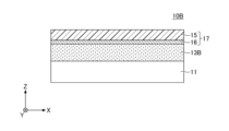
- 10A to 10C are diagrams illustrating another example of a layer structure of the electromagnetic wave reflecting panel according to the embodiment.
- FIG. 13 is a diagram showing the layer structure of an electromagnetic wave reflective panel using a metal mesh for comparison.
- the reflection function layer is formed of a conductive layer provided on a resin film, thereby suppressing the haze of the electromagnetic wave reflection panel and maintaining high transparency.
- the haze of the electromagnetic wave reflection panel is 5.0% or less, preferably 2.5% or less.
- the transmittance for visible light is 70% or more, preferably 75% or more, and more preferably 80% or more.
- the conductive layer may be formed as a solid film or a patterned film on the resin film by sputtering, vacuum deposition, or the like. Alternatively, it may be formed as a patterned film by wet etching a metal foil attached to the resin film via an adhesive. The surface resistivity of the conductive layer thus formed is 0.5 ⁇ /sq.
- the surface resistivity and film thickness of the conductive layer is set to an appropriate range so that the visible light transmittance and reflection characteristics are maintained at a high level.
- FIG. 1 is a schematic diagram of an electromagnetic wave reflecting device 60 using an electromagnetic wave reflecting panel 10 according to an embodiment.
- the electromagnetic wave reflecting device 60 has the electromagnetic wave reflecting panel 10 and a frame 50 that holds the electromagnetic wave reflecting panel 10.
- the width or horizontal direction of the electromagnetic wave reflecting panel 10 is the X direction
- the height or vertical direction is the Y direction
- the thickness direction is the Z direction.
- the electromagnetic wave reflecting panel 10 reflects electromagnetic waves from the gigahertz band to the terahertz band, such as microwaves, millimeter waves, and submillimeter waves, and is transparent to visible light.
- the visible light transmittance is 70% or more, preferably 75% or more, and more preferably 80% or more.
- the electromagnetic wave reflection panel 10 has a conductive layer formed on a resin film as a reflection function layer, as described below.
- the resin film is a transparent, heat-resistant film such as polyethylene terephthalate (PET), polycarbonate (PC), cycloolefin polymer (COP), or polyimide (PI).
- the conductive layer is formed of a metal with low visible light absorption, such as Ag, Pt, Rh, Pd, or Al, a good conductor such as Cu, or a transparent conductive oxide such as ITO or IZO. From the viewpoint of transparency to visible light and electrical resistance, Ag is particularly preferred.
- sputtering may be performed on the resin film at room temperature or low temperature, or a combination of vacuum deposition and etching may be used, or a combination of lamination of metal foil and etching may be used.
- the surface resistivity of the conductive layer constituting the reflective functional layer is 0.5 ⁇ /sq. or more and less than 60.0 ⁇ /sq., preferably 0.5 ⁇ /sq. or more and 50.0 ⁇ /sq. or less.
- the thickness of the conductive layer is 10 nm or more and 1000 nm or less, preferably 30 nm or more and 500 nm or less. It is practically difficult to form a transparent conductive film with a surface resistivity of less than 0.5 ⁇ /sq. If the surface resistivity is 60.0 ⁇ /sq. or more, the loss exceeds the allowable range and the reflection characteristics deteriorate. If the thickness of the conductive layer is less than 10 nm, the surface resistivity increases.
- the thickness of the conductive layer exceeds 1000 nm, the visible light transmittance decreases.
- a low surface resistivity and high visible light transmittance can be obtained by making the thickness 30 nm or more and 700 nm or less, preferably 50 nm or more and 500 nm or less.
- the frame 50 holds two sides along the height direction of the electromagnetic wave reflection panel 10 when it is installed.
- a top frame 57 that holds the upper end of the electromagnetic wave reflection panel 10 and a bottom frame 58 that holds the lower end may be provided.
- the frame 50, the top frame 57, and the bottom frame 58 form a frame that holds the entire circumference of the electromagnetic wave reflection panel 10.
- the frame 50 may be called a "side frame” based on its positional relationship with the top frame 57 and the bottom frame 58.
- Legs 56 that support the frame 50 may be provided. As shown in FIG. 1, it is desirable to provide the legs 56 when the electromagnetic wave reflection device 60 is to be freestanding on the installation surface, but the legs 56 are not essential. Casters may be provided on the legs 56 to make it mobile, or the electromagnetic wave reflection panel 10 may be installed on a wall surface or hung from the ceiling without providing the legs 56.
- FIG. 2 is a schematic diagram of an electromagnetic wave reflecting fence 100 in which electromagnetic wave reflecting devices 60-1, 60-2, and 60-3 are connected.
- three electromagnetic wave reflecting devices 60-1, 60-2, and 60-3 (hereinafter, collectively referred to as “electromagnetic wave reflecting devices 60" as appropriate) are connected to form the electromagnetic wave reflecting fence 100, but there is no particular limit to the number of electromagnetic wave reflecting devices 60 that are connected.
- Electromagnetic wave reflecting devices 60-1, 60-2, and 60-3 each have electromagnetic wave reflecting panels 10-1, 10-2, and 10-3. Adjacent electromagnetic wave reflecting panels are held together by a frame 50 to obtain an electromagnetic wave reflecting fence 100 connected in the X direction.
- Each of the electromagnetic wave reflecting panels 10-1, 10-2, and 10-3 (hereinafter sometimes collectively referred to as "electromagnetic wave reflecting panel 10") has a reflecting function layer made of a conductive layer formed on a resin film. By having this reflecting function layer, the electromagnetic wave reflecting panel 10 has a lower haze and higher transparency than a configuration in which a metal mesh is used for the reflecting function layer.
- ⁇ Layer structure of electromagnetic wave reflection panel> 3 shows the layer structure of the electromagnetic wave reflection panel 10A.
- the stacking direction is the thickness direction (Z direction) of the electromagnetic wave reflection panel 10A.
- a reflection function layer 17 is disposed between a first dielectric substrate 11 and a second dielectric substrate 12 via adhesive layers 13A and 14A.
- the reflection function layer 17 has a conductive layer 16 formed on a resin film 15.
- the dielectric substrate on the resin film 15 side is called the "first dielectric substrate” and the dielectric substrate on the conductive layer 16 side is called the "second dielectric substrate", but either of the two dielectric substrates may be called the "first dielectric substrate”.
- the first dielectric substrate 11 and the second dielectric substrate 12 are transparent to electromagnetic waves in the gigahertz to terahertz bands, specifically, electromagnetic waves in the range of 1 GHz to 1 THz, preferably 1 GHz to 300 GHz.
- the first dielectric substrate 11 and the second dielectric substrate 12 are desirably formed of a material having excellent impact resistance, durability, and transparency as the outermost layer of the electromagnetic wave reflection panel 10A.
- Polycarbonate, acrylic resin, PET, etc. can be used as the first dielectric substrate 11 and the second dielectric substrate 12.
- the thickness of the first dielectric substrate 11 and the second dielectric substrate 12 can be appropriately selected, for example, between 1.0 mm and 10.0 mm depending on the installation location.
- the thickness of the first dielectric substrate 11 and the second dielectric substrate 12 may be the same or different.
- the adhesive layers 13A and 14A may be a general non-carrier (base material-free) pressure sensitive adhesive or a silicone adhesive.
- Thermoplastic resins such as vinyl acetate resin, acrylic resin, cellulose resin, and silicone resin may also be used. If it is desired to give durability and moisture resistance to the adhesive layers 13A and 14A, ethylene-vinyl acetate (EVA) copolymer or COP may be used.
- the thickness of the adhesive layers 13A and 14A may be any thickness that can bond the reflective function layer 17 to the first dielectric substrate 11 and the second dielectric substrate 12, and may be appropriately selected, for example, within the range of 10 ⁇ m to 400 ⁇ m.
- the resin film 15 of the reflective function layer 17 is a transparent, heat-resistant film such as PET, PC, COP, or PI.
- the thickness of the resin film 15 may be any thickness that can support the conductive layer 16, and is 10 ⁇ m or more and 200 ⁇ m or less, preferably 30 ⁇ m or more and 150 ⁇ m or less, and more preferably 50 ⁇ m or more and 125 ⁇ m or less.
- the conductive layer 16 is formed from a metal with low visible light absorption, such as Ag, Pt, Rh, Pd, or Al, a good conductor such as Cu, or a transparent conductive oxide such as ITO or IZO. Ag is particularly preferred from the viewpoint of transmittance to visible light and low electrical resistance.
- the conductive layer 16 may be formed by sputtering on the resin film 15 at room temperature or with slight heating at 100°C or less, or a combination of vacuum deposition and etching, or lamination of metal foil and etching may be used.
- the thickness of the conductive layer 16 is appropriately designed in the range of 10 nm to 1000 nm depending on the conductive material used so that the surface resistivity is 0.5 ⁇ /sq. or more and less than 60.0 ⁇ /sq., preferably 0.5 ⁇ /sq. or more and 60.0 ⁇ /sq. or less, and the visible light transmittance is 70% or more.
- a thickness of 30 nm to 700 nm, preferably 50 nm to 500 nm can be used to obtain a low surface resistivity and a high visible light transmittance.
- the dielectric constants and dielectric loss tangents of the resin film 15 carrying the conductive layer 16, the adhesive layers 13A and 14A, the first dielectric substrate 11, and the second dielectric substrate 12 are appropriately selected for the entire laminate so as to obtain the target reflection characteristics.
- the adhesive layers 13A and 14A and the resin film 15 are transparent to electromagnetic waves in the range of 1 GHz to 1 THz, preferably 1 GHz to 300 GHz. Regardless of whether electromagnetic waves in the above bands are incident from either the first dielectric substrate 11 or the second dielectric substrate 12, they are reflected with a high reflectance by the conductive layer 16.
- the metal mesh In general lamination processing, the metal mesh is often heated to 80°C to 130°C.
- a metal mesh When a metal mesh is used as a reflective layer, the fluidity of the adhesive layer pulls the metal mesh, causing deformation and warping of the metal mesh.
- a rigid conductive layer 16 formed on the resin film 15 is used, so that even if the metal mesh is heated to the above temperature during lamination, the fluidity of the adhesive layers 13A and 14A is not affected. Therefore, the electromagnetic wave reflection panel 10A is less likely to suffer from poor appearance such as streaks and cloudiness.
- the panels may be bonded using a general non-carrier adhesive film or silicone adhesive without heat treatment.
- the above adhesive is applied to the bonding surfaces of the first dielectric substrate 11 and the second dielectric substrate 12, and the reflective functional layer 17 is sandwiched between them, so that the reflective functional layer 17 can be bonded between the first dielectric substrate 11 and the second dielectric substrate 12.
- Figure 4 shows an example of the layer structure of the electromagnetic wave reflection panel 10B.
- the stacking direction is the thickness direction (Z direction) of the electromagnetic wave reflection panel 10A.
- a reflection function layer 17 is bonded to the first dielectric substrate 11 by an adhesive layer 13B.
- the reflection function layer 17 has a conductive layer 16 formed on a resin film 15.
- the first dielectric substrate 11 and the resin film 15 are transparent to electromagnetic waves in the gigahertz to terahertz bands, specifically, electromagnetic waves in the range of 1 GHz to 1 THz, and preferably 1 GHz to 300 GHz.
- the first dielectric substrate 11 is the outermost layer of the electromagnetic wave reflecting panel 10A and is desirably formed from a material that is excellent in impact resistance, durability, and transparency.
- the first dielectric substrate 11 may be made of polycarbonate, acrylic resin, PET, or the like.
- the thickness of the first dielectric substrate 11 may be selected appropriately depending on the installation location, for example, between 1.0 mm and 10.0 mm.
- the adhesive layer 13B may be a general non-carrier (base material-free) pressure sensitive adhesive or a silicone-based adhesive.
- Thermoplastic resins such as vinyl acetate resin, acrylic resin, cellulose resin, and silicone resin may also be used. If it is desired to give durability and moisture resistance to the adhesive layer 13B, EVA copolymer or COP may be used.
- the thickness of the adhesive layer 13B may be any thickness that can bond the reflective function layer 17 to the first dielectric substrate 11, and may be appropriately selected, for example, within the range of 10 ⁇ m to 400 ⁇ m.
- the resin film 15 of the reflective functional layer 17 supports the conductive layer 16 and also serves to protect the surface of the conductive layer 16 in the laminated electromagnetic wave reflection panel 10B.
- the resin film is preferably made of a material with excellent weather resistance and transparency, and a PC film, PET film, etc. can be used.
- the electromagnetic wave reflecting panel 10B also uses a reflecting functional layer 17 including a conductive layer 16 formed on a resin film, so even if it is heated to 80°C to 130°C during lamination, the conductive layer 16 is not affected by the fluidity of the adhesive layer 13B, and poor appearance is unlikely to occur. Furthermore, the conductive layer 16 may be bonded to the first dielectric substrate 11 by applying a general non-carrier adhesive film or silicone-based adhesive to the first dielectric substrate 11 without heating at the above temperatures.
- haze and visible light transmittance are measured. Haze is measured using a commercially available haze meter such as that of Nippon Denshoku Industries Co., Ltd. Transmittance is measured using a commercially available visible light transmittance measuring device. Return loss is measured using a spectrum network analyzer and a high-frequency oblique incidence free space type S-parameter measuring jig. Electromagnetic waves of 28.0 GHz are vertically incident and vertical reflection is measured.
- Example 1 is Example 1.
- a sample having the layer structure of FIG. 3 is prepared, and the optical characteristics and return loss are measured.
- Two polycarbonate sheets having a length of 1.0 m, a width of 2.0 m, and a thickness of 2.0 mm are prepared and used as the first dielectric substrate 11 and the second dielectric substrate 12.
- a layer in which an Ag film having a thickness of 350 nm is sputtered on a PET film having a thickness of 100 ⁇ m is used as the reflective functional layer 17.
- the surface resistivity of the Ag film measured by the four-probe method is 0.8 ⁇ /sq.
- This reflective functional layer is sandwiched between two polycarbonate sheets using EVA having a thickness of 400 ⁇ m as an adhesive layer and laminated.
- the sample is heated at a temperature of 100° C.
- the haze of the sample after lamination is 1.0%
- the visible light transmittance is 70.0%
- the return loss at a frequency of 28.0 GHz is ⁇ 0.35 dB.
- the sample in Example 1 has a low haze of 1.0% and is highly transparent.
- the surface resistivity can be reduced to 0.8 ⁇ /sq., but the visible light transmittance is 70.0%, which is within the acceptable range.
- the Ag film is used as the reflective functional layer, the return loss for electromagnetic waves of 28.0 GHz is only -0.35 dB, and the reflective properties are comparable to those of a 3.0 mm thick aluminum plate.
- Example 2 is Example 2.
- the sample of Example 2 also has the layer structure of FIG. 3, but the thickness of the resin film and the conductive layer of the reflective functional layer are changed.
- Two polycarbonate sheets with a length of 1.0 m, a width of 2.0 m, and a thickness of 2.0 mm are prepared and used as the first dielectric substrate 11 and the second dielectric substrate 12.
- As the reflective functional layer 17 a layer in which a 100 nm thick Ag film is sputtered on a 50 ⁇ m thick PET film is used.
- the surface resistivity of the Ag film measured by the four-probe method is 5.0 ⁇ /sq.
- This reflective functional layer is sandwiched between two polycarbonate sheets using a 400 ⁇ m thick EVA as an adhesive layer and laminated.
- the laminate is heated at a temperature of 100° C.
- the haze of the sample after lamination is 0.8%, and the visible light transmittance is 80.0%.
- the return loss at a frequency of 28.0 GHz is ⁇ 0.50 dB.
- the sample in Example 2 has a low haze of 0.8% and is highly transparent.
- the surface resistivity was 5.0 ⁇ /sq., but the visible light transmittance was improved to 80.0%.
- the return loss for electromagnetic waves of 28.0 GHz is small at -0.50 dB, and the reflective characteristics are comparable to those of a 3.0 mm thick aluminum plate.
- the sample is heated at a temperature of 100° C.
- the haze of the sample after lamination is 1.2%
- the visible light transmittance is 80.0%
- the return loss at a frequency of 28.0 GHz is ⁇ 0.51 dB.
- Example 4 is Example 4.
- the sample of Example 4 also has the layer structure of FIG. 3, but the thickness of the resin film of the reflective functional layer and the conductive layer, and the material of the conductive layer are changed.
- Two polycarbonate sheets with a length of 1.0 m, a width of 2.0 m, and a thickness of 2.0 mm are prepared and used as the first dielectric substrate 11 and the second dielectric substrate 12.
- the surface resistivity of the ITO film measured by the four-probe method is 30.0 ⁇ /sq.
- This reflective functional layer is sandwiched between two polycarbonate sheets using EVA with a thickness of 400 ⁇ m as an adhesive layer and laminated.
- EVA adhesive layer
- the sample is heated at a temperature of 100° C.
- the haze of the sample after lamination treatment was 1.3%, the visible light transmittance was 85.0%, and the return loss at a frequency of 28.0 GHz was as small as -1.54 dB.
- the sample in Example 4 uses ITO for the conductive film of the reflective functional layer, so it has a low haze of 1.3%, a high visible light transmittance of 85%, and high transparency.
- the surface resistivity is 30.0 ⁇ /sq., which is well within the acceptable range. Because an ITO film is used for the reflective functional layer, the return loss for electromagnetic waves of 28.0 GHz is small at -1.54 dB.
- Example 5 is Example 5.
- the sample of Example 5 adopts the layer structure of FIG. 4 and is laminated without heating.
- a polycarbonate sheet having a length of 1.0 m, a width of 2.0 m, and a thickness of 2.0 mm is used as the first dielectric substrate 11.
- the same configuration as in Example 1 is used as the reflective functional layer 17. That is, a layer in which a 50 nm thick Ag film is sputtered on a 100 ⁇ m thick PET film is used.
- the surface resistivity of the Ag film measured by the four-probe method is 10.0 ⁇ /sq.
- An acrylic adhesive having a thickness of 25 ⁇ m is used as the adhesive layer 13B to bond the Ag film to one surface of the polycarbonate sheet.
- Example 6 is Example 6.
- the sample of Example 6 adopts the layer structure of FIG. 4 and is laminated without heating.
- a polycarbonate sheet having a length of 1.0 m, a width of 2.0 m, and a thickness of 2.0 mm is used as the first dielectric substrate 11.
- a layer in which an ITO film having a thickness of 300 nm is sputtered on a PET film having a thickness of 100 ⁇ m is used as the reflective functional layer 17.
- the surface resistivity of the ITO film measured by the four-probe method is 30.0 ⁇ /sq.
- An acrylic adhesive having a thickness of 25 ⁇ m is used as the adhesive layer 13B to bond the ITO film to one surface of the polycarbonate sheet.
- Example 7 is Example 7.
- the sample of Example 7 adopts the layer structure of FIG. 4 and is laminated without heating.
- a polycarbonate sheet having a length of 1.0 m, a width of 2.0 m, and a thickness of 2.0 mm is used as the first dielectric substrate 11.
- the surface resistivity of the Ag vapor deposition film measured by the four-probe method is 40.0 ⁇ /sq.
- the patterned Ag vapor deposition film is bonded to one surface of the polycarbonate sheet using an acrylic adhesive having a thickness of 25 ⁇ m as the adhesive layer 13B.
- the Ag vapor deposition film of the sample in Example 7 is thin at 30 nm, and the surface resistivity is higher than that of Ag sputtered films, but is well within the acceptable range.
- the return loss for electromagnetic waves of 28.0 GHz is -1.55 dB, providing sufficient reflection characteristics.
- Example 8 is Example 8.
- the sample of Example 8 adopts the layer structure of FIG. 4 and is laminated without heating.
- a polycarbonate sheet having a length of 1.0 m, a width of 2.0 m, and a thickness of 2.0 mm is used as the first dielectric substrate 11.
- the reflective functional layer 17 a copper foil having a thickness of 10 ⁇ m, which is attached to a PET film having a thickness of 100 ⁇ m via an adhesive having a thickness of 5 ⁇ m, is used which is patterned by wet etching.
- the line width of the copper foil after patterning is 10 ⁇ m, and the pitch is 300 ⁇ m.
- the surface resistivity of the copper foil pattern measured by the four-probe method is 5.0 ⁇ /sq.
- the patterned surface of the copper foil is bonded to one surface of the polycarbonate sheet. No appearance defects such as streaks or cloudiness were observed in the sample after bonding.
- the haze of the sample is 2.5%, and the visible light transmittance is 90.0%.
- an electromagnetic wave of 28.0 GHz is vertically incident from the PET film side and normal reflection is measured, the return loss is small at -0.30 dB.
- Example 8 The sample in Example 8 has a high surface resistivity compared to the Ag sputtered film, even though the copper foil is as thick as 10 ⁇ m, but this is well within the acceptable range.
- the return loss for electromagnetic waves of 28.0 GHz is -0.30 dB, providing sufficient reflection characteristics.
- Example 9 is Comparative Example 1.
- a metal mesh is used as the reflective functional layer.
- the layer structure of the sample of Example 9 is shown in FIG. 5.
- Two polycarbonate sheets, each having a length of 1.0 m, a width of 2.0 m, and a thickness of 2.0 mm, are prepared and used as the first dielectric substrate 11 and the second dielectric substrate 12.
- a stainless steel mesh 18 having a thickness of 100 ⁇ m is placed between the two polycarbonate sheets, and laminated using EVA having a thickness of 400 ⁇ m as adhesive layers 13 and 14.
- the aperture ratio of the metal mesh is 71.0%.
- the sample is heated at 110° C. during lamination processing, and then quenched at a rate of 65° C./hour to prepare a sample. When the sample was prepared, five streaks were observed with the naked eye. The haze of this sample is 7.5%, and the visible light transmittance is 55.0%.
- the return loss at a frequency of 28.0 GHz is ⁇ 0.35 dB.
- Example 9 the use of a stainless steel mesh as the reflective functional layer caused multiple streaks to appear on the sample, resulting in a high haze of 7.5%.
- the visible light transmittance was low at 55.0%.
- Increasing the mesh aperture ratio would increase the visible light transmittance, but this would likely reduce the rigidity of the mesh, resulting in more streaks and an increase in return loss. It is difficult to maintain the haze, visible light transmittance, and return loss all within the acceptable ranges when using a metal mesh.
- Example 10 is Comparative Example 2.
- a 150 nm thick ITO film formed by sputtering on a 100 ⁇ m thick PET film is used as the reflective functional layer.
- the surface resistivity of this ITO film is 60.0 ⁇ /sq.
- a reflective functional layer having an ITO film is sandwiched between two polycarbonate sheets, each having a length of 1.0 m, a width of 2.0 m, and a thickness of 2.0 mm, via an EVA adhesive layer having a thickness of 400 ⁇ m, to produce a laminate.
- the laminate is heated at 100° C. during lamination processing to obtain a sample. When the sample was produced and observed with the naked eye, no defects in appearance were observed.
- the haze of this sample is 1.0%, and the visible light transmittance is 90.0%.
- the return loss at a frequency of 28.0 GHz is ⁇ 3.50 dB, and the reflection characteristics are poor.
- Example 10 an ITO film is used for the reflective functional layer, so the haze is low and the visible light transmittance is high at 90.0%.
- the surface resistivity is high at 60.0 ⁇ /sq., and the reflective properties are poor.
- the surface resistivity is 30.0 ⁇ /sq. and the return loss is within -1.0 dB, so it is believed that by appropriately setting the film thickness of the ITO film to a surface resistivity of less than 60 ⁇ /sq., preferably 50.0 ⁇ /sq. or less, it is possible to maintain good haze, visible light transmittance, and reflective properties.
- a conductive layer of an appropriate thickness is formed on a resin film, thereby realizing an electromagnetic wave reflective panel with low haze and a visible light transmittance of 70% or more.
- the surface resistivity of the conductive layer By setting the surface resistivity of the conductive layer to 0.5 ⁇ /sq. or more and less than 60 ⁇ /sq., and preferably 0.5 ⁇ /sq. or more and 50.0 ⁇ /sq. or less, both visible light transmittance and reflective properties can be achieved.
- the thickness of the conductive layer formed on the resin film is a thickness that can achieve a surface resistivity of 0.5 ⁇ /sq. to 50.0 ⁇ /sq. and a visible light transmittance of 70% or more, depending on the conductive material used, and is typically set in the range of 10 nm to 1000 nm.
- the film thickness is 30 nm to 700 nm, more preferably 50 nm to 500 nm.
- the haze of the electromagnetic wave reflective panel can be kept low, and the visible light transmittance and reflection characteristics can be kept high.
- the layer structure of the electromagnetic wave reflective panel is not limited to the examples in Figures 3 and 4, and protective layers such as an ultraviolet protection layer and a water-repellent layer may be provided within a range that does not significantly affect the reflection characteristics and visible light transmittance.
- the above disclosure includes the following configurations.
- (Item 1) A dielectric substrate; A reflective functional layer laminated on the dielectric substrate; The reflective layer is formed of a resin film and a conductive layer provided on the resin film.
- Electromagnetic wave reflecting panel. The conductive layer is a solid film or a patterned film formed on the resin film by sputtering, vacuum deposition, or lamination of a metal foil.
- An electromagnetic wave reflecting panel according to item 1. (Item 3) an adhesive layer provided between the dielectric substrate and the reflective functional layer; 3.
- the electromagnetic wave reflecting panel according to item 1 or 2 further comprising: (Item 4) a second dielectric substrate laminated on the reflective functional layer; The reflective functional layer is sandwiched between the dielectric substrate and the second dielectric substrate.
- Item 4 An electromagnetic wave reflecting panel according to any one of items 1 to 3.
- the conductive layer of the reflective functional layer is bonded to the dielectric substrate by a first adhesive layer, The resin film is bonded to the second dielectric substrate by a second adhesive layer.
- Item 5. An electromagnetic wave reflecting panel according to item 4.
- the surface resistivity of the conductive layer is 0.5 ⁇ /sq. or more and less than 60.0 ⁇ /sq.
- Item 6 An electromagnetic wave reflecting panel according to any one of items 1 to 5.
- the dielectric substrate is transparent to frequencies of 1 GHz to 300 GHz.
- Item 7. An electromagnetic wave reflecting panel according to any one of items 1 to 6.
- the electromagnetic wave reflection panel has a haze of 5.0% or less and a visible light transmittance of 70% or more.
- Item 8 An electromagnetic wave reflecting panel according to any one of items 1 to 7.
- Item 9 An electromagnetic wave reflection panel according to any one of items 1 to 8;
- An electromagnetic wave reflecting device comprising: (Item 10) 10.
- An electromagnetic wave reflecting fence comprising a plurality of electromagnetic wave reflecting devices according to item 9 connected together by the frame.
- Electromagnetic wave reflecting panel 13A, 13B, 14, 14A Adhesive layer 15 Resin film 16 Conductive layer 17 Reflection function layer 60, 60-1, 60-2, 60-3 Electromagnetic wave reflecting device 100 Electromagnetic wave reflecting fence
Landscapes
- Physics & Mathematics (AREA)
- Engineering & Computer Science (AREA)
- Electromagnetism (AREA)
- Architecture (AREA)
- General Physics & Mathematics (AREA)
- Optics & Photonics (AREA)
- Civil Engineering (AREA)
- Structural Engineering (AREA)
- Microelectronics & Electronic Packaging (AREA)
- Laminated Bodies (AREA)
Priority Applications (1)
| Application Number | Priority Date | Filing Date | Title |
|---|---|---|---|
| JP2025521814A JPWO2024241666A1 (https=) | 2023-05-23 | 2024-03-11 |
Applications Claiming Priority (2)
| Application Number | Priority Date | Filing Date | Title |
|---|---|---|---|
| JP2023-084434 | 2023-05-23 | ||
| JP2023084434 | 2023-05-23 |
Publications (1)
| Publication Number | Publication Date |
|---|---|
| WO2024241666A1 true WO2024241666A1 (ja) | 2024-11-28 |
Family
ID=93589334
Family Applications (1)
| Application Number | Title | Priority Date | Filing Date |
|---|---|---|---|
| PCT/JP2024/009354 Ceased WO2024241666A1 (ja) | 2023-05-23 | 2024-03-11 | 電磁波反射パネル、電磁波反射装置、及び電磁波反射フェンス |
Country Status (2)
| Country | Link |
|---|---|
| JP (1) | JPWO2024241666A1 (https=) |
| WO (1) | WO2024241666A1 (https=) |
Citations (7)
| Publication number | Priority date | Publication date | Assignee | Title |
|---|---|---|---|---|
| JP2000357893A (ja) * | 1999-04-13 | 2000-12-26 | Nippon Paint Co Ltd | 電磁波シールド膜および電磁波シールド塗料 |
| JP4892207B2 (ja) * | 2005-07-25 | 2012-03-07 | 鹿島建設株式会社 | 透光性電磁波シールド板の接合構造及び接合具 |
| WO2019235536A1 (ja) * | 2018-06-07 | 2019-12-12 | マクセルホールディングス株式会社 | 電磁波吸収シート |
| WO2022102708A1 (ja) * | 2020-11-13 | 2022-05-19 | Agc株式会社 | 電磁波遮蔽体 |
| WO2022138642A1 (ja) * | 2020-12-23 | 2022-06-30 | 凸版印刷株式会社 | 電磁波抑制体 |
| WO2022196338A1 (ja) * | 2021-03-16 | 2022-09-22 | Agc株式会社 | 電磁波反射装置、電磁波反射フェンス、及び電磁波反射装置の組み立て方法 |
| WO2023042799A1 (ja) * | 2021-09-16 | 2023-03-23 | 凸版印刷株式会社 | 電磁波抑制体 |
-
2024
- 2024-03-11 WO PCT/JP2024/009354 patent/WO2024241666A1/ja not_active Ceased
- 2024-03-11 JP JP2025521814A patent/JPWO2024241666A1/ja active Pending
Patent Citations (7)
| Publication number | Priority date | Publication date | Assignee | Title |
|---|---|---|---|---|
| JP2000357893A (ja) * | 1999-04-13 | 2000-12-26 | Nippon Paint Co Ltd | 電磁波シールド膜および電磁波シールド塗料 |
| JP4892207B2 (ja) * | 2005-07-25 | 2012-03-07 | 鹿島建設株式会社 | 透光性電磁波シールド板の接合構造及び接合具 |
| WO2019235536A1 (ja) * | 2018-06-07 | 2019-12-12 | マクセルホールディングス株式会社 | 電磁波吸収シート |
| WO2022102708A1 (ja) * | 2020-11-13 | 2022-05-19 | Agc株式会社 | 電磁波遮蔽体 |
| WO2022138642A1 (ja) * | 2020-12-23 | 2022-06-30 | 凸版印刷株式会社 | 電磁波抑制体 |
| WO2022196338A1 (ja) * | 2021-03-16 | 2022-09-22 | Agc株式会社 | 電磁波反射装置、電磁波反射フェンス、及び電磁波反射装置の組み立て方法 |
| WO2023042799A1 (ja) * | 2021-09-16 | 2023-03-23 | 凸版印刷株式会社 | 電磁波抑制体 |
Also Published As
| Publication number | Publication date |
|---|---|
| JPWO2024241666A1 (https=) | 2024-11-28 |
Similar Documents
| Publication | Publication Date | Title |
|---|---|---|
| CN112622391B (zh) | 一种光学透明超宽带雷达与红外双隐身结构 | |
| JP2022169557A (ja) | ガラス用アンテナユニット、アンテナ付きガラス板、およびガラス用アンテナユニットの製造方法 | |
| JP7622746B2 (ja) | 電波吸収体 | |
| JP6601199B2 (ja) | 透明導電体 | |
| JP7638232B2 (ja) | 透過性アンテナ積層体及びアセンブリ | |
| KR20180042543A (ko) | 필름 적층물 및 이를 포함하는 윈도우 제조물 | |
| EP2593820A1 (en) | Thin films for energy efficient transparent electromagnetic shields | |
| WO2021241455A1 (ja) | アンテナユニット及び窓ガラス | |
| CN114122738A (zh) | 一种基于ito电阻膜的透明宽带电磁吸波器 | |
| KR102007723B1 (ko) | 열차단 필름 | |
| WO2024241666A1 (ja) | 電磁波反射パネル、電磁波反射装置、及び電磁波反射フェンス | |
| KR20140110909A (ko) | 레이다 반사-흡수 글레이징 | |
| JP7255179B2 (ja) | 熱線遮蔽合わせガラス | |
| JP6550860B2 (ja) | 透明発熱板、暖房器具及び住宅用窓 | |
| JP2018001554A (ja) | 赤外線反射性積層体および閉鎖部材 | |
| WO2022030395A1 (ja) | 周波数選択表面装荷部材および車両用窓部材 | |
| WO2025041555A1 (ja) | 電磁波反射パネル、これを用いた電磁波反射装置、電磁波反射フェンス、電磁波反射パネルの製造方法、及び電磁波反射パネルの評価方法 | |
| JPH11150393A (ja) | 透明電波吸収体およびその作製方法 | |
| WO2025100388A1 (ja) | 電磁波反射フィルム | |
| WO2024214372A1 (ja) | 電磁波反射パネルの製造方法、電磁波反射パネル、電磁波反射装置、及び電磁波反射フェンス | |
| WO2024214374A1 (ja) | 電磁波反射パネルの製造方法、電磁波反射パネル、電磁波反射装置、及び電磁波反射フェンス | |
| WO2024195270A1 (ja) | 電磁波反射パネル、電磁波反射装置、電磁波反射フェンス、及び電磁波反射パネルの製造方法 | |
| WO2024190085A1 (ja) | 電磁波反射パネル、電磁波反射装置、電磁波反射フェンス、及び電磁波反射パネルの製造方法 | |
| CN224093246U (zh) | 隔热膜及窗结构体 | |
| CN119895663A (zh) | 反射面板、使用其的电磁波反射装置、电磁波反射围栏以及反射面板的制作方法 |
Legal Events
| Date | Code | Title | Description |
|---|---|---|---|
| 121 | Ep: the epo has been informed by wipo that ep was designated in this application |
Ref document number: 24810674 Country of ref document: EP Kind code of ref document: A1 |
|
| ENP | Entry into the national phase |
Ref document number: 2025521814 Country of ref document: JP Kind code of ref document: A |
|
| WWE | Wipo information: entry into national phase |
Ref document number: 2025521814 Country of ref document: JP |
|
| NENP | Non-entry into the national phase |
Ref country code: DE |