WO2024237161A1 - 半導体積層体および光半導体素子 - Google Patents
半導体積層体および光半導体素子 Download PDFInfo
- Publication number
- WO2024237161A1 WO2024237161A1 PCT/JP2024/017231 JP2024017231W WO2024237161A1 WO 2024237161 A1 WO2024237161 A1 WO 2024237161A1 JP 2024017231 W JP2024017231 W JP 2024017231W WO 2024237161 A1 WO2024237161 A1 WO 2024237161A1
- Authority
- WO
- WIPO (PCT)
- Prior art keywords
- semiconductor layer
- type
- type semiconductor
- layer
- concentration
- Prior art date
- Legal status (The legal status is an assumption and is not a legal conclusion. Google has not performed a legal analysis and makes no representation as to the accuracy of the status listed.)
- Ceased
Links
Images

Classifications
-
- H—ELECTRICITY
- H01—ELECTRIC ELEMENTS
- H01S—DEVICES USING THE PROCESS OF LIGHT AMPLIFICATION BY STIMULATED EMISSION OF RADIATION [LASER] TO AMPLIFY OR GENERATE LIGHT; DEVICES USING STIMULATED EMISSION OF ELECTROMAGNETIC RADIATION IN WAVE RANGES OTHER THAN OPTICAL
- H01S5/00—Semiconductor lasers
- H01S5/04—Processes or apparatus for excitation, e.g. pumping, e.g. by electron beams
- H01S5/042—Electrical excitation ; Circuits therefor
-
- H—ELECTRICITY
- H10—SEMICONDUCTOR DEVICES; ELECTRIC SOLID-STATE DEVICES NOT OTHERWISE PROVIDED FOR
- H10H—INORGANIC LIGHT-EMITTING SEMICONDUCTOR DEVICES HAVING POTENTIAL BARRIERS
- H10H20/00—Individual inorganic light-emitting semiconductor devices having potential barriers, e.g. light-emitting diodes [LED]
- H10H20/80—Constructional details
- H10H20/81—Bodies
- H10H20/811—Bodies having quantum effect structures or superlattices, e.g. tunnel junctions
-
- H—ELECTRICITY
- H10—SEMICONDUCTOR DEVICES; ELECTRIC SOLID-STATE DEVICES NOT OTHERWISE PROVIDED FOR
- H10H—INORGANIC LIGHT-EMITTING SEMICONDUCTOR DEVICES HAVING POTENTIAL BARRIERS
- H10H20/00—Individual inorganic light-emitting semiconductor devices having potential barriers, e.g. light-emitting diodes [LED]
- H10H20/80—Constructional details
- H10H20/81—Bodies
- H10H20/816—Bodies having carrier transport control structures, e.g. highly-doped semiconductor layers or current-blocking structures
Definitions
- This disclosure relates to a semiconductor laminate and an optical semiconductor element.
- a semiconductor laminate including a structure (pn junction) in which an n-type semiconductor layer with n-type conductivity and a p-type semiconductor layer with p-type conductivity are in contact and laminated can be used to manufacture various semiconductor elements.
- a laser diode structure including a p-type semiconductor layer and an n-type semiconductor layer that form a tunnel junction has been proposed (Non-Patent Document 1).
- the semiconductor laminate according to the present disclosure comprises a first p-type semiconductor layer made of a III-V compound semiconductor and having a p-type conductivity, and a first n-type semiconductor layer made of a III-V compound semiconductor and having an n-type conductivity, laminated on the first p-type semiconductor layer so as to be in contact with the first p-type semiconductor layer.
- the first p-type semiconductor layer contains carbon as an acceptor. In the first n-type semiconductor layer, carbon functions as a donor.
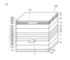
- FIG. 1 is a schematic cross-sectional view showing the structure of a semiconductor laminate.
- FIG. 2 is a schematic diagram showing the structure of a semiconductor laser.
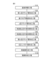
- FIG. 3 is a flow chart showing an outline of a method for manufacturing a semiconductor laminate and a semiconductor laser.
- the n-type semiconductor layer contains donors (n-type impurities that generate electrons, which are majority carriers).
- the p-type semiconductor layer contains acceptors (p-type impurities that generate holes, which are majority carriers).
- the donors of the n-type semiconductor layer diffuse from the n-type semiconductor layer to the p-type semiconductor layer.
- the acceptors of the p-type semiconductor layer diffuse from the p-type semiconductor layer to the n-type semiconductor layer. In this way, there is a problem that the mutual diffusion of impurities reduces the carrier concentration in the p-type semiconductor layer and the n-type semiconductor layer, and increases the resistance at the pn junction.
- one of the objectives of this disclosure is to provide a semiconductor laminate and an optical semiconductor element that can suppress an increase in resistance due to interdiffusion of impurities between a p-type semiconductor layer and an n-type semiconductor layer.
- the first p-type semiconductor layer contains carbon as an acceptor. In the first n-type semiconductor layer, carbon functions as a donor.
- the semiconductor laminate of the present disclosure when carbon contained as an acceptor in the first p-type semiconductor layer diffuses into the first n-type semiconductor layer, it functions as a donor in the first n-type semiconductor layer. In other words, carbon that diffuses into the first n-type semiconductor layer generates electrons, which are majority carriers in the first n-type semiconductor layer.
- the mobility of electrons, which are majority carriers in the first n-type semiconductor layer is high and has a large effect on the resistance at the pn junction. Therefore, according to the semiconductor laminate of the present disclosure, it is possible to suppress an increase in resistance caused by mutual diffusion of impurities between the first p-type semiconductor layer and the first n-type semiconductor layer.
- the first n-type semiconductor layer may contain silicon, tellurium, or sulfur as a donor. Silicon, tellurium, and sulfur are all suitable donors to be contained in the first n-type semiconductor layer.
- the first n-type semiconductor layer may contain carbon as a donor.
- the carbon contained as a donor in the first n-type semiconductor layer diffuses into the first p-type semiconductor layer, it functions as an acceptor in the first p-type semiconductor layer. Therefore, it is possible to further suppress an increase in resistance caused by mutual diffusion of impurities between the first p-type semiconductor layer and the first n-type semiconductor layer.
- the first n-type semiconductor layer may be composed of In1 - xGaxAsyP1 -y , where 0 ⁇ x ⁇ 0.3 and 0 ⁇ y ⁇ 1 are satisfied.
- carbon functions as a donor. Therefore, such a first n-type semiconductor layer is suitable as the first n-type semiconductor layer of the present disclosure.
- the carrier concentration of the first n-type semiconductor layer may be 1 ⁇ 10 18 cm ⁇ 3 or more.
- the carrier concentration of the first p-type semiconductor layer may be 1 ⁇ 10 18 cm ⁇ 3 or more.
- the first n-type semiconductor layer may have a carrier concentration of 1 ⁇ 10 19 cm ⁇ 3 or more.
- the first p-type semiconductor layer may have a carrier concentration of 1 ⁇ 10 19 cm ⁇ 3 or more.
- the first n-type semiconductor layer and the first p-type semiconductor layer may form a tunnel junction.
- the semiconductor laminate of the present disclosure is particularly suitable for a semiconductor laminate including a tunnel junction that requires a first n-type semiconductor layer and a first p-type semiconductor layer with high carrier concentrations.
- the semiconductor laminate may further include a second n-type semiconductor layer made of a III-V compound semiconductor and having an n-type conductivity type, an active layer made of a III-V compound semiconductor, a second p-type semiconductor layer made of a III-V compound semiconductor and having a p-type conductivity type, and a third n-type semiconductor layer made of a III-V compound semiconductor and having an n-type conductivity type.
- the second n-type semiconductor layer, the active layer, the second p-type semiconductor layer, the first p-type semiconductor layer, the first n-type semiconductor layer, and the third n-type semiconductor layer may be laminated in this order.
- Such a semiconductor laminate may be used in the manufacture of an optical semiconductor element.
- the optical semiconductor element according to the present disclosure comprises: (8) An optical semiconductor element according to the present disclosure, comprising the semiconductor laminate according to (7) above and an electrode disposed on the third n-type semiconductor layer, the optical semiconductor element according to the present disclosure including the semiconductor laminate according to the present disclosure, can suppress an increase in resistance caused by interdiffusion of impurities between the first p-type semiconductor layer and the first n-type semiconductor layer.
- the composition wavelength of the first n-type semiconductor layer and the first p-type semiconductor layer may be shorter than the emission wavelength of the optical semiconductor element. This configuration makes it possible to prevent the light generated in the active layer from being absorbed by the first n-type semiconductor layer and the first p-type semiconductor layer.
- the "composition wavelength" of the semiconductor layer means the wavelength of light equivalent to the band gap energy determined by the composition of the semiconductor layer.
- the semiconductor laminate 1 in one embodiment of the present disclosure includes, in order, a substrate 11, a first n-type cladding layer 12, an active layer 20, a p-type cladding layer 30, a high-concentration p-type semiconductor layer 41, a high-concentration n-type semiconductor layer 42, a second n-type cladding layer 50, and an n-type contact layer 60.
- the high-concentration p-type semiconductor layer 41 is made of a III-V compound semiconductor and is a first p-type semiconductor layer with a p-type conductivity.
- the high-concentration n-type semiconductor layer 42 is made of a III-V compound semiconductor and is a first n-type semiconductor layer with an n-type conductivity.
- the first n-type cladding layer 12 is a second n-type semiconductor layer with an n-type conductivity.
- the p-type cladding layer 30 is a second p-type semiconductor layer with a p-type conductivity.
- the second n-type cladding layer 50 and the n-type contact layer 60 are a third n-type semiconductor layer with an n-type conductivity.
- the substrate 11 is made of a III-V group compound semiconductor.
- the diameter of the substrate 11 is 50 mm or more, for example, 3 inches.
- the diameter of the substrate 11 can be 80 mm or more (for example, 4 inches), further 100 mm or more (for example, 5 inches), and further 130 mm or more (for example, 6 inches) for the purpose of improving the production efficiency and yield of semiconductor devices such as optical semiconductor elements using the semiconductor laminate 1.
- As the n-type impurity contained in the substrate 11, for example, S (sulfur) can be adopted.
- the substrate 11 has a higher impurity concentration than the first n-type cladding layer 12, and therefore has a higher carrier concentration than the first n-type cladding layer 12.
- the n-type carrier concentration of the substrate 11 is, for example, 1 ⁇ 10 17 cm ⁇ 3 or more and 1 ⁇ 10 19 cm ⁇ 3 or less.
- the substrate 11 has a first major surface 11A and a second major surface 11B.
- carrier concentration refers to the concentration of carriers (holes or electrons) generated by impurities contained in a semiconductor, excluding inactive impurities.
- Carrier concentration can be measured, for example, using an ECV-pro, an ECV (Electrochemical Capacitance-Voltage) measuring device manufactured by Nanometrics.
- the first n-type cladding layer 12 is disposed so as to be in contact with the second main surface 11B of the substrate 11.
- the first n-type cladding layer 12 is made of a III-V group compound semiconductor.
- InP can be adopted as the III-V group compound semiconductor constituting the first n-type cladding layer 12.
- the first n-type cladding layer 12 has a first main surface 12A and a second main surface 12B.
- InP (n-InP) having an n-type conductivity type is adopted as the compound semiconductor constituting the first n-type cladding layer 12.
- S or the like can be adopted as the n-type impurity contained in the first n-type cladding layer 12.
- the n-type carrier concentration of the first n-type cladding layer 12 is, for example, 1 ⁇ 10 17 cm ⁇ 3 or more and 1 ⁇ 10 19 cm ⁇ 3 or less.
- the first n-type cladding layer 12 is in contact with the second main surface 11B of the substrate 11 at the first main surface 12A.
- the active layer 20 is arranged so as to be in contact with the second main surface 12B of the first n-type cladding layer 12.
- the active layer 20 has a structure in which a plurality of element layers made of III-V group compound semiconductors are stacked. More specifically, the active layer 20 may be a SCH-MQW (Separate Confinement Heterostructure Multiple Quantum Well) including, for example, an InGaAs (indium gallium arsenide) layer and an InGaAsP (indium gallium arsenide phosphide) layer.
- the active layer 20 has a first main surface 20A and a second main surface 20B. The active layer 20 is in contact with the second main surface 12B of the first n-type cladding layer 12 at the first main surface 20A.
- the p-type cladding layer 30 has a first main surface 30A and a second main surface 30B.
- the p-type cladding layer 30 is disposed so that the first main surface 30A is in contact with the second main surface 20B of the active layer 20.
- the p-type cladding layer 30 is made of a III-V group compound semiconductor.
- InP can be used as the III-V group compound semiconductor constituting the p-type cladding layer 30.
- InP (p-InP) having a p-type conductivity is used as the compound semiconductor constituting the p-type cladding layer 30.
- Zn (zinc) can be used as the p-type impurity contained in the p-type cladding layer 30.
- DEZn diethyl zinc
- DMZn dimethyl zinc
- the p-type carrier concentration of the p-type cladding layer 30 is, for example, 1 ⁇ 10 17 cm ⁇ 3 or more and 1 ⁇ 10 19 cm ⁇ 3 or less.
- the high-concentration p-type semiconductor layer 41 has a first major surface 41A and a second major surface 41B.
- the high-concentration p-type semiconductor layer 41 is disposed so as to contact the second major surface 30B of the p-type cladding layer 30 at the first major surface 41A.
- the high-concentration p-type semiconductor layer 41 is made of a III-V group compound semiconductor.
- the high-concentration p-type semiconductor layer 41 has a p-type conductivity type by containing a high concentration of p-type impurities.
- the high-concentration p-type semiconductor layer 41 contains carbon (C) as an acceptor (p-type impurity).
- carbon is a dopant of the high-concentration p-type semiconductor layer 41, and the concentration of carbon is, for example, 1 ⁇ 10 18 cm ⁇ 3 or more.
- the III-V group compound semiconductor III-V group compound semiconductor in which carbon functions as an acceptor
- the value of x can be 0.38 or more and 1 or less.
- AlXInYGa1 -X-YAs aluminum indium gallium arsenide
- the value of X can be set to 0 or more and 0.62 or less
- the value of Y can be set to 0.38 or more and 1 or less.
- the high-concentration n-type semiconductor layer 42 has a first major surface 42A and a second major surface 42B.
- the high-concentration n-type semiconductor layer 42 is disposed so as to contact the second major surface 41B of the high-concentration p-type semiconductor layer 41 at the first major surface 42A.
- the high-concentration n-type semiconductor layer 42 is made of a III-V group compound semiconductor.
- the high-concentration n-type semiconductor layer 42 has an n-type conductivity type by containing a high concentration of n-type impurities. In 1-x Ga x As y P 1-y can be adopted as the III-V group compound semiconductor constituting the high-concentration n-type semiconductor layer 42.
- the high-concentration n-type semiconductor layer 42 contains a high concentration of Si (silicon) as an n-type impurity that generates electrons, which are majority carriers. Te (tellurium), S (sulfur), or the like may be adopted as the n-type impurity of the high-concentration n-type semiconductor layer 42 instead of Si (silicon). Furthermore, the high-concentration n-type semiconductor layer 42 may contain carbon diffused from the high-concentration p-type semiconductor layer 41.
- the carbon concentration of the high-concentration n-type semiconductor layer 42 is smaller than that of the high-concentration p-type semiconductor layer 41, and although it varies depending on the carbon concentration in the high-concentration p-type semiconductor layer 41, it is at most 1 ⁇ 10 19 cm ⁇ 3 .
- carbon functions as a donor. That is, even if carbon, which is a dopant (acceptor) of the high-concentration p-type semiconductor layer 41, diffuses into the high-concentration n-type semiconductor layer 42, the carbon functions as a donor in the high-concentration n-type semiconductor layer 42. Therefore, the effective carrier concentration does not decrease due to impurity diffusion, and an increase in resistance can be suppressed.
- the p-type carrier concentration of the high-concentration p-type semiconductor layer 41 is 1 ⁇ 10 19 cm ⁇ 3 or more.
- the n-type carrier concentration of the high-concentration n-type semiconductor layer 42 is 1 ⁇ 10 19 cm ⁇ 3 or more.
- the high-concentration p-type semiconductor layer 41 and the high-concentration n-type semiconductor layer 42 form a tunnel junction. That is, electrons in the valence band of the high-concentration p-type semiconductor layer 41 are replaced by electrons in the conduction band of the high-concentration n-type semiconductor layer 42 by the tunnel effect.
- the p-type carrier concentration of the high-concentration p-type semiconductor layer 41 can be, for example, 1 ⁇ 10 20 cm ⁇ 3 or less.
- the n-type carrier concentration of the high-concentration n-type semiconductor layer 42 can be, for example, 1 ⁇ 10 20 cm ⁇ 3 or less.
- the second n-type cladding layer 50 has a first main surface 50A and a second main surface 50B.
- the second n-type cladding layer 50 is disposed so as to be in contact with the second main surface 42B of the high-concentration n-type semiconductor layer 42 at the first main surface 50A.
- the second n-type cladding layer 50 is made of a III-V group compound semiconductor.
- InP can be used as the III-V group compound semiconductor constituting the second n-type cladding layer 50.
- InP (n-InP) having an n-type conductivity type is used as the compound semiconductor constituting the second n-type cladding layer 50.
- the n-type carrier concentration of the second n-type cladding layer 50 is, for example, 1 ⁇ 10 17 cm ⁇ 3 or more and 1 ⁇ 10 19 cm ⁇ 3 or less.
- the n-type contact layer 60 has a first major surface 60A and a second major surface 60B.
- the n-type contact layer 60 is disposed so that the first major surface 60A is in contact with the second major surface 50B of the second n-type cladding layer 50.
- the n-type contact layer 60 is made of a III-V group compound semiconductor.
- InP can be used as the III-V group compound semiconductor constituting the n-type contact layer 60.
- InP (n-InP) having an n-type conductivity type is used as the compound semiconductor constituting the n-type contact layer 60.
- S or the like can be used as the n-type impurity contained in the n-type contact layer 60.
- the n-type contact layer 60 has a higher impurity concentration than the second n-type cladding layer 50, and therefore has a higher carrier concentration than the second n-type cladding layer 50.
- the n-type carrier concentration of the n-type contact layer 60 is, for example, 1 ⁇ 10 18 cm ⁇ 3 or more and 1 ⁇ 10 20 cm ⁇ 3 or less.
- the semiconductor laminate 1 of this embodiment includes a high-concentration p-type semiconductor layer 41 and a high-concentration n-type semiconductor layer 42 that form a tunnel junction. This makes it possible to configure the region located on the opposite side of the active layer 20 from the high-concentration p-type semiconductor layer 41 and the high-concentration n-type semiconductor layer 42 with the second n-type cladding layer 50 and the n-type contact layer 60, which are n-type semiconductor layers.
- n-type semiconductor layers tend to have a smaller contact resistance with an electrode than p-type semiconductor layers.
- n-type semiconductor layers tend to absorb less light than p-type semiconductor layers. For this reason, for example, a highly efficient semiconductor laser can be obtained by forming an electrode in contact with the n-type contact layer 60 of the semiconductor laminate 1 of this embodiment to fabricate a semiconductor laser, which is an optical semiconductor device.
- the carbon contained as an acceptor in the high-concentration p-type semiconductor layer 41 diffuses into the high-concentration n-type semiconductor layer 42, it functions as a donor in the high-concentration n-type semiconductor layer 42.
- the carbon that diffuses into the high-concentration n-type semiconductor layer 42 generates electrons, which are the majority carriers in the high-concentration n-type semiconductor layer 42. Therefore, according to the semiconductor laminate 1 of this embodiment, it is possible to suppress an increase in resistance caused by mutual diffusion of impurities between the high-concentration p-type semiconductor layer 41 and the high-concentration n-type semiconductor layer 42.
- the semiconductor laser 100 of this embodiment is fabricated using the semiconductor laminate 1 of this embodiment, and includes a substrate 11, a first n-type cladding layer 12, an active layer 20, a p-type cladding layer 30, a high-concentration p-type semiconductor layer 41, a high-concentration n-type semiconductor layer 42, a second n-type cladding layer 50, and an n-type contact layer 60.
- the semiconductor laser 100 further includes an insulating film 70, a first electrode 81, and a second electrode 82.
- the insulating film 70 is disposed so as to be in contact with the second major surface 60B of the n-type contact layer 60.
- the insulating film 70 is made of an insulator such as silicon nitride or silicon oxide.
- the insulating film 70 has a first major surface 70A and a second major surface 70B.
- the insulating film 70 has an opening 70C formed therein, penetrating the insulating film 70 in the thickness direction.
- the first electrode 81 is disposed so as to be in contact with the second major surface 70B of the insulating film 70.
- the first electrode 81 is made of a conductor such as a metal. More specifically, the first electrode 81 can be made of a metal layer in which, for example, a Ti (titanium) layer, a Pt (platinum) layer, and an Au (gold) layer are laminated in this order.
- the first electrode 81 fills the opening 70C formed in the insulating film 70. As a result, the first electrode 81 is in contact with the second major surface 60B of the n-type contact layer 60 exposed in the opening 70C.
- the first electrode 81 is in ohmic contact with the n-type contact layer 60.
- the second electrode 82 is disposed so as to be in contact with the first main surface 11A of the substrate 11.
- the second electrode 82 is made of a conductor such as a metal. More specifically, the second electrode 82 can be made of a metal layer in which, for example, a Ti layer, a Pt layer, and an Au layer are laminated in this order.
- the second electrode 82 is in ohmic contact with the substrate 11.
- the semiconductor laser 100 is an edge-emitting laser diode having a Fabry-Perot structure.
- the semiconductor laser 100 of this embodiment includes the semiconductor laminate 1 of this embodiment. Therefore, the semiconductor laser 100 includes a high-concentration p-type semiconductor layer 41 and a high-concentration n-type semiconductor layer 42 that form a tunnel junction, and an increase in resistance due to mutual diffusion of impurities between the high-concentration p-type semiconductor layer 41 and the high-concentration n-type semiconductor layer 42 is suppressed, making it a highly efficient optical semiconductor element.
- the composition wavelength of the high-concentration p-type semiconductor layer 41 and the high-concentration n-type semiconductor layer 42 is preferably shorter than the emission wavelength of the semiconductor laser 100.
- This configuration makes it possible to suppress the light generated in the active layer 20 from being absorbed by the high-concentration p-type semiconductor layer 41 and the high-concentration n-type semiconductor layer 42. As a result, the efficiency of the semiconductor laser 100 can be further improved.
- a substrate preparation step is first performed as step S10.
- step S10 referring to FIG. 1, a substrate 11 made of InP having an n-type conductivity is prepared. More specifically, an ingot made of InP is sliced to obtain the substrate 11 made of InP. The surface of the substrate 11 is polished, and then the substrate 11 is prepared through a process such as cleaning, ensuring the flatness and cleanliness of the second main surface 11B.
- a first n-type cladding layer formation step is carried out as step S20.
- the first n-type cladding layer 12 made of, for example, n-InP, a III-V compound semiconductor, is formed by vapor phase epitaxy (for example, metal organic vapor phase epitaxy) so as to be in contact with the second main surface 11B of the substrate 11.
- vapor phase epitaxy for example, metal organic vapor phase epitaxy
- TMIn trimethylindium
- TBP tertiary butyl phosphine
- an active layer 20 which is an SCH-MQW including, for example, an InGaAs layer and an InGaAsP layer, is formed by vapor phase growth so as to be in contact with the second main surface 12B of the first n-type cladding layer 12.
- TMIn can be used as the In raw material.
- TEGa triethylgallium
- TBAs tertiarybutylarsine
- TBP tertiarybutylphosphine
- a p-type cladding layer formation step is carried out as step S40.
- the p-type cladding layer 30 is formed by vapor phase growth so as to be in contact with the second main surface 20B of the active layer 20.
- TMIn can be used as the In source material.
- TBP can be used as the P source material.
- a high-concentration p-type semiconductor layer forming step is performed as step S50.
- a high-concentration p-type semiconductor layer 41 made of, for example, In x Ga 1-x As is formed so as to be in contact with the second main surface 30B of the p-type cladding layer 30.
- TMIn can be used as a source of In.
- TEGa can be used as a source of Ga.
- TBAs can be used as a source of As.
- CBr 4 carbon tetrabromide
- CBr 4 carbon tetrabromide
- a high-concentration n-type semiconductor layer forming step is performed as step S60.
- a high-concentration n-type semiconductor layer 42 made of In 1-x Ga x As y P 1-y (0 ⁇ x ⁇ 0.3 and 0 ⁇ y ⁇ 1) is formed so as to contact the second main surface 41B of the high-concentration p-type semiconductor layer 41.
- TMIn can be used as a source of In.
- TEGa can be used as a source of Ga.
- TBAs can be used as a source of As.
- TBP tertiary butyl phosphine
- SiH 4 (silane), TeESi (tetraethyl silane), etc. can be used as a source of Si as an n-type impurity.
- a second n-type cladding layer formation step is carried out as step S70.
- the second n-type cladding layer 50 is formed by vapor phase growth so as to be in contact with the second main surface 42B of the high-concentration n-type semiconductor layer 42.
- TMIn can be used as the In source material.
- TBP can be used as the P source material.
- an n-type contact layer formation step is performed as step S80.
- the n-type contact layer 60 is formed by vapor phase growth so as to be in contact with the second main surface 50B of the second n-type cladding layer 50.
- TMIn can be used as the In source.
- TBP can be used as the P source.
- an insulating film forming step is carried out as step S90 on the semiconductor laminate 1 obtained by carrying out steps S10 to S80.
- an insulating film 70 is formed on the second main surface 60B of the n-type contact layer 60.
- the insulating film 70 made of an insulator such as silicon oxide or silicon nitride is formed by, for example, CVD (Chemical Vapor Deposition).
- step S100 an electrode formation step is performed as step S100.
- a first electrode 81 and a second electrode 82 are formed on the semiconductor laminate 1 on which the insulating film 70 has been formed.
- a mask having an opening on a region where the opening 70C of the insulating film 70 is to be formed is first formed on the insulating film 70.
- the opening 70C is formed in the insulating film 70 using the mask.
- the first electrode 81 and the second electrode 82 made of an appropriate conductor are formed by, for example, a deposition method.
- the semiconductor laser 100 in this embodiment is completed. Thereafter, it is separated into each element by, for example, dicing.
- the semiconductor layers are formed by a vapor phase epitaxy method such as metal organic vapor phase epitaxy.
- a vapor phase epitaxy method such as metal organic vapor phase epitaxy.
- the formation of each semiconductor layer may also be achieved by, for example, a molecular beam epitaxy (MBE) method.
- MBE molecular beam epitaxy
- the high-concentration n-type semiconductor layer 42 contains Si (silicon), Te (tellurium), or S (sulfur) as a donor
- C carbon
- carbon may be the dopant of the high-concentration n-type semiconductor layer 42.
- the semiconductor laminate 1 of this embodiment includes the high-concentration p-type semiconductor layer 41 and the high-concentration n-type semiconductor layer 42 that constitute a tunnel junction, and the increase in resistance due to the mutual diffusion of impurities between the high-concentration p-type semiconductor layer 41 and the high-concentration n-type semiconductor layer 42 is suppressed.
- the semiconductor laminate 1 of this embodiment is a semiconductor laminate that can contribute to improving the efficiency of semiconductor elements.
- the carrier concentration of the high-concentration p-type semiconductor layer 41 and the high-concentration n-type semiconductor layer 42 corresponding to the first p-type semiconductor layer and the first n-type semiconductor layer of the present disclosure, respectively, is described as 1 ⁇ 10 19 cm ⁇ 3 or more, but the carrier concentration of the first p-type semiconductor layer and the first n-type semiconductor layer is not limited to this range.
- the carrier concentration of the first p-type semiconductor layer and the first n-type semiconductor layer may be, for example, 1 ⁇ 10 16 cm ⁇ 3 or more and 1 ⁇ 10 19 cm ⁇ 3 or less.
- the influence of mutual diffusion of impurities on the resistance is large, so that the effect of adopting the first p-type semiconductor layer and the first n-type semiconductor layer having the characteristics of the present disclosure is large.
- a laser diode semiconductor laser
- a semiconductor laminate suitable for fabricating a laser diode is exemplified, but the optical semiconductor element of the present disclosure is not limited to a laser diode.
- the optical semiconductor element of the present disclosure may be, for example, an LED (Light Emitting Diode) or a solar cell.
Landscapes
- Physics & Mathematics (AREA)
- Condensed Matter Physics & Semiconductors (AREA)
- General Physics & Mathematics (AREA)
- Electromagnetism (AREA)
- Optics & Photonics (AREA)
- Semiconductor Lasers (AREA)
Priority Applications (1)
| Application Number | Priority Date | Filing Date | Title |
|---|---|---|---|
| JP2025520537A JPWO2024237161A1 (https=) | 2023-05-12 | 2024-05-09 |
Applications Claiming Priority (2)
| Application Number | Priority Date | Filing Date | Title |
|---|---|---|---|
| JP2023079312 | 2023-05-12 | ||
| JP2023-079312 | 2023-05-12 |
Publications (1)
| Publication Number | Publication Date |
|---|---|
| WO2024237161A1 true WO2024237161A1 (ja) | 2024-11-21 |
Family
ID=93519095
Family Applications (1)
| Application Number | Title | Priority Date | Filing Date |
|---|---|---|---|
| PCT/JP2024/017231 Ceased WO2024237161A1 (ja) | 2023-05-12 | 2024-05-09 | 半導体積層体および光半導体素子 |
Country Status (2)
| Country | Link |
|---|---|
| JP (1) | JPWO2024237161A1 (https=) |
| WO (1) | WO2024237161A1 (https=) |
Citations (3)
| Publication number | Priority date | Publication date | Assignee | Title |
|---|---|---|---|---|
| JP2007053376A (ja) * | 2005-08-15 | 2007-03-01 | Avago Technologies Ecbu Ip (Singapore) Pte Ltd | 半導体素子の作動電圧を低下させるための構造 |
| JP2009059918A (ja) * | 2007-08-31 | 2009-03-19 | Sumitomo Electric Ind Ltd | 光半導体デバイス |
| US20180006189A1 (en) * | 2016-06-29 | 2018-01-04 | Epileds Technologies, Inc. | Epitaxial structure with tunnel junction, p-side up processing intermediate structure and method of manufacturing the same |
Family Cites Families (6)
| Publication number | Priority date | Publication date | Assignee | Title |
|---|---|---|---|---|
| JPH06152056A (ja) * | 1992-11-10 | 1994-05-31 | Fujitsu Ltd | 半導体レーザ |
| JPH0815213B2 (ja) * | 1993-01-14 | 1996-02-14 | 日本電気株式会社 | 電界効果トランジスタ |
| JP3421836B2 (ja) * | 1998-07-14 | 2003-06-30 | 日本電信電話株式会社 | 半導体装置の製造方法 |
| KR20070023453A (ko) * | 2005-08-24 | 2007-02-28 | 삼성전자주식회사 | 스토리지 노드의 특성을 개선할 수 있는 반도체 메모리소자의 제조 방법 |
| JP2008235574A (ja) * | 2007-03-20 | 2008-10-02 | Sumitomo Electric Ind Ltd | 面発光半導体レーザ |
| JP2008235519A (ja) * | 2007-03-20 | 2008-10-02 | Nippon Telegr & Teleph Corp <Ntt> | 光半導体素子及び光半導体素子の作製方法 |
-
2024
- 2024-05-09 JP JP2025520537A patent/JPWO2024237161A1/ja active Pending
- 2024-05-09 WO PCT/JP2024/017231 patent/WO2024237161A1/ja not_active Ceased
Patent Citations (3)
| Publication number | Priority date | Publication date | Assignee | Title |
|---|---|---|---|---|
| JP2007053376A (ja) * | 2005-08-15 | 2007-03-01 | Avago Technologies Ecbu Ip (Singapore) Pte Ltd | 半導体素子の作動電圧を低下させるための構造 |
| JP2009059918A (ja) * | 2007-08-31 | 2009-03-19 | Sumitomo Electric Ind Ltd | 光半導体デバイス |
| US20180006189A1 (en) * | 2016-06-29 | 2018-01-04 | Epileds Technologies, Inc. | Epitaxial structure with tunnel junction, p-side up processing intermediate structure and method of manufacturing the same |
Also Published As
| Publication number | Publication date |
|---|---|
| JPWO2024237161A1 (https=) | 2024-11-21 |
Similar Documents
| Publication | Publication Date | Title |
|---|---|---|
| CN102292833B (zh) | Iii-v族化合物半导体受光元件 | |
| JPH1056201A (ja) | 基板構造、発光装置、基板構造の製造方法および発光装置の製造方法 | |
| US11894502B2 (en) | Method of manufacturing semiconductor optical device and intermediate article of semiconductor optical device | |
| JP2009059918A (ja) | 光半導体デバイス | |
| US7583715B2 (en) | Semiconductor conductive layers | |
| JP5463760B2 (ja) | 光導波路集積型半導体光素子およびその製造方法 | |
| US20080253422A1 (en) | Surface emitting semiconductor laser | |
| JP4172505B2 (ja) | 面発光型半導体素子及び面発光型半導体素子の製造方法 | |
| CN103125054A (zh) | 光电装置 | |
| US11329453B2 (en) | Surface emitting laser | |
| CN101453100B (zh) | 集成型半导体光元件 | |
| WO2015011966A1 (ja) | 垂直共振器型面発光レーザおよびその製造方法 | |
| JP6702523B1 (ja) | 半導体装置 | |
| US20230096932A1 (en) | Surface emitting laser | |
| JPH11284280A (ja) | 半導体レーザ装置及びその製造方法ならびにiii−v族化合物半導体素子の製造方法 | |
| WO2024237161A1 (ja) | 半導体積層体および光半導体素子 | |
| US20200028328A1 (en) | Vertical cavity surface emitting laser | |
| US20040013146A1 (en) | Laser diode with a low absorption diode junction | |
| JP2006253212A (ja) | 半導体レーザ | |
| JP6200158B2 (ja) | 半導体発光素子およびその製造方法 | |
| JP2005260109A (ja) | 光半導体素子 | |
| EP4568030A1 (en) | Semiconductor laminate, semiconductor element, and method for producing semiconductor laminate | |
| JP2020098891A (ja) | 半導体レーザ | |
| JP4508174B2 (ja) | 垂直共振型面発光素子 | |
| JP2008135667A (ja) | 半導体装置 |
Legal Events
| Date | Code | Title | Description |
|---|---|---|---|
| 121 | Ep: the epo has been informed by wipo that ep was designated in this application |
Ref document number: 24807113 Country of ref document: EP Kind code of ref document: A1 |
|
| ENP | Entry into the national phase |
Ref document number: 2025520537 Country of ref document: JP Kind code of ref document: A |
|
| WWE | Wipo information: entry into national phase |
Ref document number: 2025520537 Country of ref document: JP |
|
| NENP | Non-entry into the national phase |
Ref country code: DE |