WO2024237037A1 - 多層基板及び電子機器 - Google Patents
多層基板及び電子機器 Download PDFInfo
- Publication number
- WO2024237037A1 WO2024237037A1 PCT/JP2024/015875 JP2024015875W WO2024237037A1 WO 2024237037 A1 WO2024237037 A1 WO 2024237037A1 JP 2024015875 W JP2024015875 W JP 2024015875W WO 2024237037 A1 WO2024237037 A1 WO 2024237037A1
- Authority
- WO
- WIPO (PCT)
- Prior art keywords
- conductor layer
- layer
- signal line
- resin layer
- conductor
- Prior art date
- Legal status (The legal status is an assumption and is not a legal conclusion. Google has not performed a legal analysis and makes no representation as to the accuracy of the status listed.)
- Ceased
Links
Images






Classifications
-
- H—ELECTRICITY
- H05—ELECTRIC TECHNIQUES NOT OTHERWISE PROVIDED FOR
- H05K—PRINTED CIRCUITS; CASINGS OR CONSTRUCTIONAL DETAILS OF ELECTRIC APPARATUS; MANUFACTURE OF ASSEMBLAGES OF ELECTRICAL COMPONENTS
- H05K1/00—Printed circuits
- H05K1/02—Details
- H05K1/0213—Electrical arrangements not otherwise provided for
- H05K1/0237—High frequency adaptations
- H05K1/024—Dielectric details, e.g. changing the dielectric material around a transmission line
-
- H—ELECTRICITY
- H01—ELECTRIC ELEMENTS
- H01P—WAVEGUIDES; RESONATORS, LINES, OR OTHER DEVICES OF THE WAVEGUIDE TYPE
- H01P3/00—Waveguides; Transmission lines of the waveguide type
- H01P3/02—Waveguides; Transmission lines of the waveguide type with two longitudinal conductors
- H01P3/08—Microstrips; Strip lines
-
- H—ELECTRICITY
- H05—ELECTRIC TECHNIQUES NOT OTHERWISE PROVIDED FOR
- H05K—PRINTED CIRCUITS; CASINGS OR CONSTRUCTIONAL DETAILS OF ELECTRIC APPARATUS; MANUFACTURE OF ASSEMBLAGES OF ELECTRICAL COMPONENTS
- H05K1/00—Printed circuits
- H05K1/02—Details
-
- H—ELECTRICITY
- H05—ELECTRIC TECHNIQUES NOT OTHERWISE PROVIDED FOR
- H05K—PRINTED CIRCUITS; CASINGS OR CONSTRUCTIONAL DETAILS OF ELECTRIC APPARATUS; MANUFACTURE OF ASSEMBLAGES OF ELECTRICAL COMPONENTS
- H05K1/00—Printed circuits
- H05K1/02—Details
- H05K1/0213—Electrical arrangements not otherwise provided for
- H05K1/0216—Reduction of cross-talk, noise or electromagnetic interference
- H05K1/0218—Reduction of cross-talk, noise or electromagnetic interference by printed shielding conductors, ground planes or power plane
-
- H—ELECTRICITY
- H05—ELECTRIC TECHNIQUES NOT OTHERWISE PROVIDED FOR
- H05K—PRINTED CIRCUITS; CASINGS OR CONSTRUCTIONAL DETAILS OF ELECTRIC APPARATUS; MANUFACTURE OF ASSEMBLAGES OF ELECTRICAL COMPONENTS
- H05K1/00—Printed circuits
- H05K1/02—Details
- H05K1/0213—Electrical arrangements not otherwise provided for
- H05K1/0216—Reduction of cross-talk, noise or electromagnetic interference
- H05K1/0218—Reduction of cross-talk, noise or electromagnetic interference by printed shielding conductors, ground planes or power plane
- H05K1/0219—Printed shielding conductors for shielding around or between signal conductors, e.g. coplanar or coaxial printed shielding conductors
-
- H—ELECTRICITY
- H05—ELECTRIC TECHNIQUES NOT OTHERWISE PROVIDED FOR
- H05K—PRINTED CIRCUITS; CASINGS OR CONSTRUCTIONAL DETAILS OF ELECTRIC APPARATUS; MANUFACTURE OF ASSEMBLAGES OF ELECTRICAL COMPONENTS
- H05K1/00—Printed circuits
- H05K1/02—Details
- H05K1/0213—Electrical arrangements not otherwise provided for
- H05K1/0216—Reduction of cross-talk, noise or electromagnetic interference
- H05K1/0218—Reduction of cross-talk, noise or electromagnetic interference by printed shielding conductors, ground planes or power plane
- H05K1/0224—Patterned shielding planes, ground planes or power planes
-
- H—ELECTRICITY
- H05—ELECTRIC TECHNIQUES NOT OTHERWISE PROVIDED FOR
- H05K—PRINTED CIRCUITS; CASINGS OR CONSTRUCTIONAL DETAILS OF ELECTRIC APPARATUS; MANUFACTURE OF ASSEMBLAGES OF ELECTRICAL COMPONENTS
- H05K1/00—Printed circuits
- H05K1/02—Details
- H05K1/0213—Electrical arrangements not otherwise provided for
- H05K1/0216—Reduction of cross-talk, noise or electromagnetic interference
- H05K1/0218—Reduction of cross-talk, noise or electromagnetic interference by printed shielding conductors, ground planes or power plane
- H05K1/0224—Patterned shielding planes, ground planes or power planes
- H05K1/0225—Single or multiple openings in a shielding, ground or power plane
-
- H—ELECTRICITY
- H05—ELECTRIC TECHNIQUES NOT OTHERWISE PROVIDED FOR
- H05K—PRINTED CIRCUITS; CASINGS OR CONSTRUCTIONAL DETAILS OF ELECTRIC APPARATUS; MANUFACTURE OF ASSEMBLAGES OF ELECTRICAL COMPONENTS
- H05K1/00—Printed circuits
- H05K1/02—Details
- H05K1/0213—Electrical arrangements not otherwise provided for
- H05K1/0237—High frequency adaptations
-
- H—ELECTRICITY
- H05—ELECTRIC TECHNIQUES NOT OTHERWISE PROVIDED FOR
- H05K—PRINTED CIRCUITS; CASINGS OR CONSTRUCTIONAL DETAILS OF ELECTRIC APPARATUS; MANUFACTURE OF ASSEMBLAGES OF ELECTRICAL COMPONENTS
- H05K1/00—Printed circuits
- H05K1/02—Details
- H05K1/0213—Electrical arrangements not otherwise provided for
- H05K1/0237—High frequency adaptations
- H05K1/0242—Structural details of individual signal conductors, e.g. related to the skin effect
-
- H—ELECTRICITY
- H05—ELECTRIC TECHNIQUES NOT OTHERWISE PROVIDED FOR
- H05K—PRINTED CIRCUITS; CASINGS OR CONSTRUCTIONAL DETAILS OF ELECTRIC APPARATUS; MANUFACTURE OF ASSEMBLAGES OF ELECTRICAL COMPONENTS
- H05K1/00—Printed circuits
- H05K1/02—Details
- H05K1/0213—Electrical arrangements not otherwise provided for
- H05K1/0237—High frequency adaptations
- H05K1/025—Impedance arrangements, e.g. impedance matching, reduction of parasitic impedance
-
- H—ELECTRICITY
- H05—ELECTRIC TECHNIQUES NOT OTHERWISE PROVIDED FOR
- H05K—PRINTED CIRCUITS; CASINGS OR CONSTRUCTIONAL DETAILS OF ELECTRIC APPARATUS; MANUFACTURE OF ASSEMBLAGES OF ELECTRICAL COMPONENTS
- H05K1/00—Printed circuits
- H05K1/02—Details
- H05K1/0213—Electrical arrangements not otherwise provided for
- H05K1/0237—High frequency adaptations
- H05K1/025—Impedance arrangements, e.g. impedance matching, reduction of parasitic impedance
- H05K1/0253—Impedance adaptations of transmission lines by special lay-out of power planes, e.g. providing openings
-
- H—ELECTRICITY
- H05—ELECTRIC TECHNIQUES NOT OTHERWISE PROVIDED FOR
- H05K—PRINTED CIRCUITS; CASINGS OR CONSTRUCTIONAL DETAILS OF ELECTRIC APPARATUS; MANUFACTURE OF ASSEMBLAGES OF ELECTRICAL COMPONENTS
- H05K1/00—Printed circuits
- H05K1/02—Details
- H05K1/0296—Conductive pattern lay-out details not covered by sub groups H05K1/02 - H05K1/0295
- H05K1/0298—Multilayer circuits
-
- H—ELECTRICITY
- H05—ELECTRIC TECHNIQUES NOT OTHERWISE PROVIDED FOR
- H05K—PRINTED CIRCUITS; CASINGS OR CONSTRUCTIONAL DETAILS OF ELECTRIC APPARATUS; MANUFACTURE OF ASSEMBLAGES OF ELECTRICAL COMPONENTS
- H05K3/00—Apparatus or processes for manufacturing printed circuits
- H05K3/46—Manufacturing multilayer circuits
-
- H—ELECTRICITY
- H05—ELECTRIC TECHNIQUES NOT OTHERWISE PROVIDED FOR
- H05K—PRINTED CIRCUITS; CASINGS OR CONSTRUCTIONAL DETAILS OF ELECTRIC APPARATUS; MANUFACTURE OF ASSEMBLAGES OF ELECTRICAL COMPONENTS
- H05K3/00—Apparatus or processes for manufacturing printed circuits
- H05K3/46—Manufacturing multilayer circuits
- H05K3/4611—Manufacturing multilayer circuits by laminating two or more circuit boards
- H05K3/4626—Manufacturing multilayer circuits by laminating two or more circuit boards characterised by the insulating layers or materials
- H05K3/4632—Manufacturing multilayer circuits by laminating two or more circuit boards characterised by the insulating layers or materials laminating thermoplastic or uncured resin sheets comprising printed circuits without added adhesive materials between the sheets
-
- H—ELECTRICITY
- H05—ELECTRIC TECHNIQUES NOT OTHERWISE PROVIDED FOR
- H05K—PRINTED CIRCUITS; CASINGS OR CONSTRUCTIONAL DETAILS OF ELECTRIC APPARATUS; MANUFACTURE OF ASSEMBLAGES OF ELECTRICAL COMPONENTS
- H05K3/00—Apparatus or processes for manufacturing printed circuits
- H05K3/46—Manufacturing multilayer circuits
- H05K3/4688—Composite multilayer circuits, i.e. comprising insulating layers having different properties
-
- H—ELECTRICITY
- H05—ELECTRIC TECHNIQUES NOT OTHERWISE PROVIDED FOR
- H05K—PRINTED CIRCUITS; CASINGS OR CONSTRUCTIONAL DETAILS OF ELECTRIC APPARATUS; MANUFACTURE OF ASSEMBLAGES OF ELECTRICAL COMPONENTS
- H05K3/00—Apparatus or processes for manufacturing printed circuits
- H05K3/46—Manufacturing multilayer circuits
- H05K3/4697—Manufacturing multilayer circuits having cavities, e.g. for mounting components
-
- H—ELECTRICITY
- H05—ELECTRIC TECHNIQUES NOT OTHERWISE PROVIDED FOR
- H05K—PRINTED CIRCUITS; CASINGS OR CONSTRUCTIONAL DETAILS OF ELECTRIC APPARATUS; MANUFACTURE OF ASSEMBLAGES OF ELECTRICAL COMPONENTS
- H05K2201/00—Indexing scheme relating to printed circuits covered by H05K1/00
- H05K2201/07—Electric details
- H05K2201/0707—Shielding
- H05K2201/0715—Shielding provided by an outer layer of PCB
Definitions
- the present invention relates to a multilayer substrate having a cavity and an electronic device equipped with the multilayer substrate.
- a high-speed transmission board using a flex board made of copper foil and a resin insulating substrate is disclosed in Patent Document 1, for example.
- This high-speed transmission board has high-speed transmission signal wiring, and is a laminated board made of a substrate surrounded by an air layer.
- the laminated unit substrate is a flex board with a structure in which an adhesive made of a thermoplastic resin is applied between the copper foil and the resin insulating substrate, and on the underside of the resin insulating substrate.
- Patent Document 1 requires an adhesive layer to ensure the adhesion of the copper foil.
- the surface of copper foil is generally roughened to improve adhesion, but at high frequencies, the roughening increases the skin resistance, resulting in large transmission losses.
- the object of the present invention is to provide a multilayer board in which the signal line passes through a cavity, i.e., the signal line is partially in contact with the cavity, and in which the high-frequency characteristics of the signal line in the cavity where the signal line is not supported are improved, and an electronic device equipped with this multilayer board.
- a multilayer board is formed by laminating layers including a plurality of conductor-layer-forming resin layers, each of which has a conductor layer formed on a main surface of a resin layer, the conductor layer-forming resin layer includes a first conductor layer-forming resin layer having a first conductor layer formed on one main surface, and a second conductor layer-forming resin layer having a second conductor layer formed on one main surface, At least a portion of the first conductor layer is a signal line, At least a portion of the second conductor layer is a GND electrode, When viewed in the lamination direction, there is a hollow portion in the first conductor layer-forming resin layer, the hollow portion being free of resin in the resin layer in a region including a position where the signal line overlaps, and whereby the signal line is exposed; The thickness of the signal line in the cavity is thinner than the thickness of the first conductor layer other than the cavity.
- a multilayer board is formed by laminating layers including a plurality of conductor-layer-forming resin layers, each of which has a conductor layer formed on a main surface of a resin layer, the conductor layer-forming resin layer includes a first conductor layer-forming resin layer having a first conductor layer formed on one main surface, and a second conductor layer-forming resin layer having a second conductor layer formed on one main surface, At least a portion of the first conductor layer is a signal line, At least a portion of the second conductor layer is a GND electrode, When viewed in the lamination direction, there is a hollow portion in the second conductor layer-forming resin layer, the hollow portion being absent of resin in the resin layer in a region including a position where the signal line overlaps, and exposing the GND electrode, The thickness of the GND electrode in the cavity is formed to be thinner than the thickness of the GND electrode other than the cavity.
- An example of an electronic device is a device that includes the multilayer substrate and a processing unit that processes high-frequency signals propagating through the multilayer substrate.
- the multilayer board of the present invention provides a multilayer board having a structure in which a signal line is partially in contact with a cavity, in which the high frequency characteristics of the signal line in the cavity where the signal line is not supported are improved, and an electronic device equipped with this multilayer board.
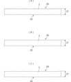
- 1A, 1B, and 1C are cross-sectional views of conductor layers that form a part of a multilayer substrate according to a first embodiment.
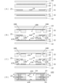
- 2A, 2B, 2C, and 2D are cross-sectional views of the multilayer substrate according to the first embodiment at various stages in the manufacture thereof.
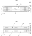
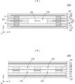
- 3A and 3B are cross-sectional views of a multilayer substrate 101 according to the first embodiment.
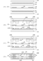
- 4A, 4B, and 4C are cross-sectional views of conductor layers that form part of a multilayer substrate according to a second embodiment.
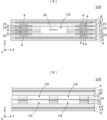
- 5A and 5B are cross-sectional views of a multilayer substrate 102 according to the second embodiment.
- 6A, 6B, and 6C are cross-sectional views of conductor layers that form part of a multilayer substrate according to a third embodiment.
- 7A and 7B are cross-sectional views of a multilayer substrate 103 according to the third embodiment.
- 8A, 8B, and 8C are cross-sectional views of conductor layers that form a part of a multilayer substrate according to a fourth embodiment.
- 9A and 9B are cross-sectional views of a multilayer substrate 104 according to the fourth embodiment.
- 10A, 10B, and 10C are cross-sectional views of conductor layers that form part of a multilayer substrate according to a fifth embodiment.
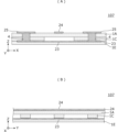
- 11A and 11B are cross-sectional views of a multilayer substrate 105 according to the sixth embodiment.
- 12A and 12B are cross-sectional views of a multilayer substrate 106 according to the seventh embodiment.
- FIG. 13A and 13B are cross-sectional views of a multilayer substrate 107 according to the eighth embodiment.
- 14A and 14B are cross-sectional views of a multilayer substrate 108 according to the ninth embodiment.
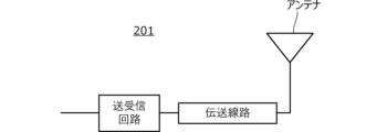
- FIG. 15 is a block diagram showing the configuration of an electronic device 201 according to the ninth embodiment.
- the multilayer board according to the first aspect of the present invention is a multilayer board including a plurality of conductor-layer-forming resin layers, each having a conductor layer formed on a main surface of the resin layer, and may include a layer of a single resin layer that does not include a conductor layer as necessary.
- the conductor-layer-forming resin layer includes a first conductor-layer-forming resin layer having a first conductor layer formed on one main surface, and a second conductor-layer-forming resin layer having a second conductor layer formed on one main surface. At least a part of the first conductor layer is a signal line, and at least a part of the second conductor layer is a GND electrode.
- the thickness of the signal line in the cavity is formed thinner by etching or the like than the thickness of the first conductor layer other than the cavity.
- the multilayer board according to the second aspect of the present invention is a multilayer board including a plurality of conductor layer-forming resin layers, each having a conductor layer formed on a main surface of the resin layer, and optionally including a layer of a single resin layer that does not include a conductor layer.
- the conductor layer-forming resin layer includes a first conductor layer-forming resin layer having a first conductor layer formed on one main surface, and a second conductor layer-forming resin layer having a second conductor layer formed on one main surface. At least a part of the first conductor layer is a signal line, and at least a part of the second conductor layer is a GND electrode.
- the thickness of the GND electrode in the cavity is formed thinner by etching or the like than the thickness of the GND electrode outside the cavity.
- First Embodiment 1(A), 1(B), and 1(C) are cross-sectional views of a conductor layer constituting a part of a multilayer substrate according to a first embodiment.
- the conductor layer 2 is, for example, a copper foil, and has one main surface 2R and the other main surface 2S. However, hatching is omitted in these figures.
- the state shown in FIG. 1(A) is a cross-sectional view of the conductor layer 2 before processing (initial state), with one main surface 2R being a rough surface and the other main surface 2S being a smooth surface.
- the state shown in FIG. 1(B) is a cross-sectional view of the conductor layer 2 in a state where it has been smoothed to a certain extent, with one main surface 2R having a rough surface that has been smoothed to a certain extent, and the other main surface 2S having a smooth surface.
- the state shown in FIG. 1(C) is a cross-sectional view of the conductor layer 2 in a further smoothened state, with both the main surface 2R and the other main surface 2S having a smoothened surface.
- the conductor layer 2 is, for example, copper foil.
- the one main surface 2R and the other main surface 2S in the above state are each effectively used.
- FIGS. 2(A), 2(B), 2(C), and 2(D) are cross-sectional views at each stage during the manufacture of a multilayer board according to this embodiment.
- FIG. 2(D) is a cross-sectional view at the completion of manufacture.
- the rough surface which is one of the main surfaces of each resin layer, is shown as having a simple array of protrusions.
- the smooth surface, which is the other main surface of each resin layer is shown as a simple straight line.
- the multilayer substrate 101 of this embodiment shown in FIG. 2(D) includes one resin layer 1D, 1E in which no conductor layer is formed, and one first conductor layer-forming resin layer 31 and two second conductor layer-forming resin layers 32 in which a conductor layer is formed, as shown in FIG. 2(A).
- the manufacturing method for the multilayer substrate 101 is as follows.
- the layers before lamination include resin layer 1E, lower second conductor layer-forming resin layer 32, first conductor layer-forming resin layer 31, upper second conductor layer-forming resin layer 32, and resin layer 1D.
- the first conductor layer-forming resin layer 31 is a layer in which a signal line 24 and a GND electrode 25 are formed on resin layer 1A.
- the upper second conductor layer-forming resin layer 32 is a layer in which a GND electrode 23 is formed on resin layer 1B.
- the lower second conductor layer-forming resin layer 32 is a layer in which a GND electrode 23 is formed on resin layer 1C.
- resin removal sections 1AR are formed in multiple locations on resin layer 1A.
- Resin removal sections 1BR are formed in multiple locations on resin layer 1B.
- resin removal sections 1CR are formed in multiple locations on resin layer 1C.
- the signal line 24 and the GND electrode 25 of one of the first conductor layer-forming resin layers 31 shown in FIG. 2(B) are etched.
- the GND electrodes 23 of the two second conductor layer-forming resin layers 32 shown in FIG. 2(B) are each etched.
- the copper foil surface is treated with a soft etching acidic solution.
- one main surface of the GND electrode 25 remains embedded in the resin layer 1A, so the bonding strength between one main surface of the GND electrode 25 and the resin layer 1A is not reduced.
- the GND electrodes 23 of the two second conductor layer-forming resin layers 32 shown in FIG. 2(B) are etched. This makes the GND electrode 23C in the hollow portion of the GND electrode 23 in the portion opened by the resin removal portion 1BR of the resin layer 1B smooth (reducing the surface roughness), as shown in FIG. 2(C).
- the surfaces of the GND electrodes 23 and 25 may be coated to suppress oxidation of the GND electrodes.
- the surface of the signal line 24 may be coated to suppress oxidation of the signal line 24.
- gold plating or water-soluble preflux treatment may be performed.
- the surfaces of the signal line 24 and the GND electrodes 23 and 25 may be oxidized to create a copper oxide film on the surfaces.
- a corrosion prevention treatment may be applied to the surface of the signal line 24 that is exposed in the area that will later become the cavity CA.
- a corrosion prevention treatment may be applied to the surface of the GND electrode 23 that is exposed in the area that will later become the cavity CA.
- These corrosion prevention treatments include, for example, gold plating, water-soluble preflux treatment, and oxidation treatment.
- the interlayer connection conductors 4 are embedded in the resin removed portions 1AR, 1BR, and 1CR shown in FIG. 2(C), and all layers are stacked and heated as shown in FIG. 2(D) to form the multilayer board 101.
- the interlayer connection conductors 4 are a conductive paste or solder paste before heating.
- the interlayer connection conductors 4 may also be formed by drilling through holes with the layers stacked and plating the inside of the through holes with copper.
- FIGS. 3(A) and 3(B) are cross-sectional views of the multilayer substrate 101 according to this embodiment.
- FIG. 3(A) is a cross-sectional view of the multilayer substrate 101 in the same completed state as shown in FIG. 2(D). It is a cross-sectional view in the X-Z plane.
- FIG. 3(B) is a cross-sectional view in the Y-Z plane.
- the signal line 24 extends in the Y direction.
- the GND electrodes 23 and 25 also extend in the Y direction.
- the GND electrode 25 extends in the Y direction like the GND electrode 23, but the GND electrode 25 can also be formed only in the interlayer connection conductor portion.
- the interlayer connection conductor 4 shown in FIG. 3(A) provides electrical continuity between the upper and lower GND electrodes 23 via the GND electrode 25. In this way, a coaxial line is formed by surrounding the signal line 24 with the GND electrodes 23, 25.
- the interlayer connection conductors 4 are arranged at regular intervals in the extension direction of the signal line 24. These intervals are narrow enough that electromagnetic waves in the frequency band of the high-frequency signal propagating through the coaxial line hardly leak to the side (X direction).
- the GND electrodes 23, 25 (copper foil) pressed and adhered to the resin layers 1A, 1B, and 1C, respectively, are highly roughened, so the adhesion between the resin part and the copper foil is strong.
- the roughened areas of the copper foil can be easily removed by etching.
- a nickel layer is formed on the surface of the copper foil as an anti-rust layer (anti-corrosion layer), the high electrical resistance of the nickel layer can cause transmission loss problems.
- the nickel layer can be removed by the etching process described above, which also reduces transmission loss.
- the distance between the signal line 24 and the GND electrode 23 increases. Paradoxically, even if the distance between the signal line 24 and the GND electrode 23 is narrowed, the high high frequency characteristics can be maintained due to the smooth surfaces of the signal line 24 and the GND electrode 23, so a thin multilayer board can be constructed by narrowing the distance between the signal line 24 and the GND electrode 23. Even if the signal line 24 becomes thinner due to etching, the resistance value of the signal line 24 can be reduced by widening the line width of the signal line 24. This reduces transmission loss. Also, by setting the line width of the signal line 24, a transmission line with a specified characteristic impedance can be easily obtained.
- FIGS. 4(A), 4(B), and 4(C) are cross-sectional views of conductor layers that form part of the multilayer substrate according to this embodiment.
- FIG. 4(D) is a cross-sectional view of multilayer substrate 102 according to this embodiment.
- the method of manufacturing the multilayer board 102 is almost the same as that of the multilayer board 101 shown in the first embodiment.
- the states in Figs. 4(A) and 4(B) are the same as those shown in Figs. 2(A) and 2(B).
- the GND electrodes 23 of the two second conductor layer-forming resin layers 32 shown in Fig. 4(B) are etched more strongly than under the conditions shown in Fig. 2. This makes the GND electrode 23C in the hollow portion of the GND electrode 23 in the portion opened by the resin removal portion 1BR of the resin layer 1B thinner (less roughened), as shown in Fig. 4(C). This strong etching also makes the signal line 24 thinner.
- the rest of the configuration is the same as that of the multilayer substrate 101 shown in the first embodiment.
- FIGS. 5(A) and 5(B) are cross-sectional views of the multilayer substrate 102 according to this embodiment.
- FIG. 5(A) is a cross-sectional view of the multilayer substrate 102 in the same completed state as shown in FIG. 4(D). It is a cross-sectional view in the X-Z plane.
- FIG. 5(B) is a cross-sectional view in the Y-Z plane.
- the structure of the multilayer substrate 101 according to this embodiment is similar to the multilayer substrate 101 according to the first embodiment shown in FIGS. 3(A) and 3(B), but the GND electrode 23C exposed in the cavity CA is etched more strongly, so that the surface of the signal line 24 is smoother (less rough) than in the first embodiment. This strong etching also makes the signal line 24 thinner.
- the area of the GND electrode 23 exposed in the cavity CA and the signal line (copper foil) 24 are very little roughened, so the skin resistance of the signal line 24 is small and the high frequency transmission loss is small.
- the thickness inside the cavity can be made thicker, so a thinner multilayer board can be constructed.
- Figures 6(A), 6(B), and 6(C) are cross-sectional views of conductor layers constituting a portion of the multilayer substrate according to this embodiment. As shown in Figures 6(B) and 6(C), resin layers 1A, 1B, and 1C forming GND electrodes 23 and 25 have openings at locations where interlayer connection conductors 4 are to be formed.
- Figure 6(D) is a cross-sectional view of multilayer substrate 103 according to this embodiment.
- the method for manufacturing the multilayer substrate 103 is almost the same as that for the multilayer substrate 101 shown in the first embodiment.
- the method for manufacturing the multilayer substrate 103 is as follows.
- the layers before lamination are resin layer 1E, resin layer 1C on which the lower GND electrode 23 is formed, resin layer 1A on which the signal line 24 and GND electrode 25 are formed, resin layer 1F, resin layer 1B on which the upper GND electrode 23 is formed, and resin layer 1D.
- the roughened surface of the GND electrode 23 is on the surface that is not exposed in the cavity CA shown in FIG. 6(D).
- the rest of the configuration is the same as that of the multilayer substrates 101 and 102 according to the first and second embodiments.
- FIGS. 7(A) and 7(B) are cross-sectional views of the multilayer substrate 103 according to this embodiment.
- FIG. 7(A) is a cross-sectional view of the multilayer substrate 103 in the same completed state as shown in FIG. 6(D). It is a cross-sectional view in the X-Z plane.
- FIG. 7(B) is a cross-sectional view in the Y-Z plane.
- the adhesion of the GND electrode 23 to the resin layers 1D and 1E is high, so the adhesion of the surface resin layer is stronger than in the first and second embodiments. Also, since the smooth side of the copper foil of the GND electrode 23 is originally on the signal line 24 side, the skin resistance is small even without etching, and high-frequency characteristics are good. In other words, since there is no need to etch the GND electrode 23, characteristic degradation due to poor etching is less likely to occur.
- the thickness inside the cavity can be increased, which may lead to a thinner device and improved high-frequency characteristics.
- FIGS. 8(A), 8(B), and 8(C) are cross-sectional views of conductor layers that form part of the multilayer substrate according to this embodiment.
- FIG. 8(D) is a cross-sectional view of multilayer substrate 104 according to this embodiment.
- the method for manufacturing the multilayer substrate 104 is almost the same as that for the multilayer substrate 101 shown in the first embodiment.
- the method for manufacturing the multilayer substrate 104 is as follows.
- the layers before lamination are resin layer 1E, resin layer 1C on which the lower GND electrode 23 is formed, resin layer 1A on which the signal line 24 and GND electrode 25 are formed, resin layer 1B on which the upper GND electrode 23 is formed, and resin layer 1D.
- the signal line 24 remains attached to the resin layer 1A.
- the rest of the configuration is the same as that of the multilayer boards 101 and 102 according to the first and second embodiments.
- FIGS. 9(A) and 9(B) are cross-sectional views of the multilayer substrate 104 according to this embodiment.
- FIG. 9(A) is a cross-sectional view of the multilayer substrate 104 in the same completed state as shown in FIG. 8(D). It is a cross-sectional view in the X-Z plane.
- FIG. 9(B) is a cross-sectional view in the Y-Z plane.
- the roughened surface of the signal line 24 remains, but the resin layer 1A on which the signal line is formed remains, resulting in a multilayer board with high overall strength.
- the fifth embodiment differs from the fourth embodiment in that a multilayer substrate in which the roughened surface of the signal line faces the cavity portion is exemplified.
- FIGS. 10(A) and 10(B) are cross-sectional views of the multilayer substrate 105 according to this embodiment.
- FIG. 10(A) is a cross-sectional view in the X-Z plane.
- FIG. 10(B) is a cross-sectional view in the Y-Z plane.
- This multilayer board 105 includes a resin layer 1E, a lower GND electrode 23, a resin layer 1C, a signal line 24 and a GND electrode 25, a resin layer 1A, a resin layer 1F, an upper GND electrode 23, a resin layer 1B, and a resin layer 1D.
- the surface (both sides) of the signal line 24 is not roughened.
- FIGS. 11(A) and 11(B) are cross-sectional views of the multilayer substrate 106 according to this embodiment.
- FIG. 11(A) is a cross-sectional view of the multilayer substrate 106 in the X-Z plane
- FIG. 11(B) is a cross-sectional view of the multilayer substrate 106 in the Y-Z plane.
- This multilayer board 106 includes a resin layer 1E, a lower GND electrode 23, resin layers 1C and 1A, a signal line 24 and a GND electrode 25, a resin layer 1F, a resin layer 1B, an upper GND electrode 23, and a resin layer 1D.
- a cavity CA may be formed in which resin layers exist on the top, bottom, left and right sides of the inner surface.
- the GND electrode 23 is not exposed in the cavity and is covered with resin, and only the signal line 24 can have its electrode roughened in the cavity to a small extent, allowing the thickness to be reduced.
- FIGS. 12(A) and 12(B) are cross-sectional views of the multilayer substrate 107 according to this embodiment.
- FIG. 12(A) is a cross-sectional view in the X-Z plane.
- FIG. 11(B) is a cross-sectional view in the Y-Z plane.
- the multilayer board 107 of this embodiment is constructed using the resin layers 1A, 1C, and 1E shown in FIG. 8(A) in the fourth embodiment, for example.
- the multilayer board 106 of this embodiment is a multilayer board constructed by stacking the resin layers 1A, 1C, and 1E shown in FIG. 8(C).
- FIGS. 13(A) and 13(B) are cross-sectional views of the multilayer substrate 108 according to this embodiment.
- FIG. 13(A) is a cross-sectional view in the X-Z plane.
- FIG. 13(B) is a cross-sectional view in the Y-Z plane.
- the resin layer 1A on which the signal line 24 and the GND electrode 25 are formed is bonded to the resin layer 1B on which the GND electrode 23 is formed via an adhesive layer 5.
- the resin layer 1C on which the GND electrode 23 is formed is bonded to the resin layer 1A via an adhesive layer 5.
- a resist layer 6 made of a material different from the substrate is formed on the surface of the laminate.
- FIGS. 14(A) and 14(B) are cross-sectional views of the multilayer substrate 109 according to this embodiment.
- FIG. 14(A) is a cross-sectional view of the multilayer substrate 109 in the X-Z plane
- FIG. 14(B) is a cross-sectional view of the multilayer substrate 109 in the Y-Z plane.
- This multilayer board 109 includes resin layers 1A, 1B, 1C, 1G, and 1H, a lower GND electrode 23, an upper GND electrode 23, a signal line 24, a GND electrode 25, an interlayer connection conductor 4, and a resist layer 6.
- a signal line 24 and a GND electrode 25 are formed on the upper surface of resin layer 1A.
- An upper GND electrode 23 is formed on the upper surface of resin layer 1B, and a lower GND electrode 23 is formed on the lower surface of resin layer 1H.
- a GND electrode 25 is formed on the upper surface of resin layer 1C, and a GND electrode 25 is formed on the lower surface of resin layer 1G.
- a conductor layer is formed on one side of each of the resin layers 1A, 1B, 1C, 1G, and 1H.
- the surfaces of the resin layer 1A and the resin layer 1G on which no conductor layer is formed are joined together.
- both sides of the signal line 24 exposed in the cavity CA are thinned by etching, polishing, grinding, etc. With such a shape, the signal line 24 exposed in the cavity CA may be thinned.
- a resist layer 6 made of a material different from the base material is formed on the surface of the laminate. This structure protects the upper GND electrode 23 and the lower GND electrode 23 and electrically insulates them.
- FIG. 15 is a block diagram showing the main components of an electronic device according to this embodiment.
- This electronic device 201 has a transmitting/receiving circuit and an antenna, and a transmission line is provided between this transmitting/receiving circuit and the antenna.
- the transmitting/receiving circuit is an example of a "processing unit that processes high-frequency signals.”
- the transmission line in this electronic device 201 is configured with a multi-layer board according to the present invention, and is configured with the multi-layer boards shown in each of the first to seventh embodiments. High-frequency signals, for example, in the 1 GHz to 1 THz band, are propagated through this transmission line.
- the interlayer connection conductors 4 are shown to be located at the same positions above and below the GND electrode 25, but they may be located at different positions (shifted positions).
- each embodiment shows a single transmission line section, the same can be applied to a multilayer board having multiple transmission lines.
- the multilayer substrate and electronic device of the present invention may be provided in the following forms:
- a multilayer board is formed by laminating layers including a plurality of conductor-layer-forming resin layers, each of which has a conductor layer formed on a main surface of a resin layer, the conductor layer-forming resin layer includes a first conductor layer-forming resin layer having a first conductor layer formed on one main surface, and a second conductor layer-forming resin layer having a second conductor layer formed on one main surface, At least a portion of the first conductor layer is a signal line, At least a portion of the second conductor layer is a GND electrode, When viewed in the lamination direction, there is a hollow portion in the first conductor layer-forming resin layer, the hollow portion being free of resin in the resin layer in a region including a position where the signal line overlaps, and whereby the signal line is exposed; a thickness of the signal line in the cavity portion is smaller than a thickness of the first conductor layer other than the cavity portion; Multilayer board.
- a multilayer board is formed by laminating layers including a plurality of conductor-layer-forming resin layers, each of which has a conductor layer formed on a main surface of a resin layer, the conductor layer-forming resin layer includes a first conductor layer-forming resin layer having a first conductor layer formed on one main surface, and a second conductor layer-forming resin layer having a second conductor layer formed on one main surface, At least a portion of the first conductor layer is a signal line, At least a portion of the second conductor layer is a GND electrode, When viewed in the lamination direction, there is a hollow portion in the second conductor layer-forming resin layer, the hollow portion being absent of resin in the resin layer in a region including a position where the signal line overlaps, and exposing the GND electrode, a thickness of the GND electrode in the hollow portion is smaller than a thickness of the GND electrode other than the hollow portion; Multilayer board.
- a surface roughness of the signal line in the cavity portion is smaller than a surface roughness of the first conductor layer and the second conductor layer other than the cavity portion;
- a surface roughness of the GND electrode in the cavity portion is smaller than a surface roughness of the second conductor layer other than the cavity portion;
- a corrosion prevention layer is formed on a surface of the signal line that is exposed to the cavity portion;
- a corrosion prevention layer is formed on a surface of the GND electrode that is exposed to the cavity portion;
- An electronic device comprising: the multilayer substrate according to claim 7; and a processing unit that processes the high-frequency signal propagating through the multilayer substrate.
Landscapes
- Engineering & Computer Science (AREA)
- Microelectronics & Electronic Packaging (AREA)
- Physics & Mathematics (AREA)
- Electromagnetism (AREA)
- Manufacturing & Machinery (AREA)
- Production Of Multi-Layered Print Wiring Board (AREA)
Priority Applications (5)
| Application Number | Priority Date | Filing Date | Title |
|---|---|---|---|
| CN202480032467.6A CN121128319A (zh) | 2023-05-17 | 2024-04-23 | 多层基板以及电子设备 |
| DE112024002130.1T DE112024002130T5 (de) | 2023-05-17 | 2024-04-23 | Mehrschichtsubstrat und elektronische vorrichtung |
| JP2025520479A JP7823794B2 (ja) | 2023-05-17 | 2024-04-23 | 多層基板及び電子機器 |
| US19/375,775 US20260059648A1 (en) | 2023-05-17 | 2025-10-31 | Multilayer substrate and electronic device |
| JP2026021570A JP2026066370A (ja) | 2023-05-17 | 2026-02-13 | 多層基板及び電子機器 |
Applications Claiming Priority (2)
| Application Number | Priority Date | Filing Date | Title |
|---|---|---|---|
| JP2023-081874 | 2023-05-17 | ||
| JP2023081874 | 2023-05-17 |
Related Child Applications (1)
| Application Number | Title | Priority Date | Filing Date |
|---|---|---|---|
| US19/375,775 Continuation US20260059648A1 (en) | 2023-05-17 | 2025-10-31 | Multilayer substrate and electronic device |
Publications (1)
| Publication Number | Publication Date |
|---|---|
| WO2024237037A1 true WO2024237037A1 (ja) | 2024-11-21 |
Family
ID=93519008
Family Applications (1)
| Application Number | Title | Priority Date | Filing Date |
|---|---|---|---|
| PCT/JP2024/015875 Ceased WO2024237037A1 (ja) | 2023-05-17 | 2024-04-23 | 多層基板及び電子機器 |
Country Status (5)
| Country | Link |
|---|---|
| US (1) | US20260059648A1 (https=) |
| JP (2) | JP7823794B2 (https=) |
| CN (1) | CN121128319A (https=) |
| DE (1) | DE112024002130T5 (https=) |
| WO (1) | WO2024237037A1 (https=) |
Cited By (1)
| Publication number | Priority date | Publication date | Assignee | Title |
|---|---|---|---|---|
| WO2026048711A1 (ja) * | 2024-08-29 | 2026-03-05 | 株式会社村田製作所 | グラウンデッドコプレーナ導波路及び電子機器 |
Citations (4)
| Publication number | Priority date | Publication date | Assignee | Title |
|---|---|---|---|---|
| JP2003133660A (ja) * | 2001-10-19 | 2003-05-09 | G Tekku:Kk | 電源用と信号用回路が複合されたフレキシブルプリント配線板 |
| JP2021073701A (ja) * | 2016-02-26 | 2021-05-13 | ギガレーン カンパニー リミテッドGigalane Co., Ltd. | フレキシブルプリント回路基板 |
| WO2022113889A1 (ja) * | 2020-11-30 | 2022-06-02 | 株式会社村田製作所 | 伝送線路及び電子機器 |
| WO2022138355A1 (ja) * | 2020-12-24 | 2022-06-30 | 株式会社村田製作所 | 多層基板及び多層基板の製造方法 |
Family Cites Families (1)
| Publication number | Priority date | Publication date | Assignee | Title |
|---|---|---|---|---|
| JP2002118361A (ja) | 2000-10-10 | 2002-04-19 | Hitachi Cable Ltd | 高速伝送用積層基板及びその製造方法 |
-
2024
- 2024-04-23 DE DE112024002130.1T patent/DE112024002130T5/de active Pending
- 2024-04-23 CN CN202480032467.6A patent/CN121128319A/zh active Pending
- 2024-04-23 WO PCT/JP2024/015875 patent/WO2024237037A1/ja not_active Ceased
- 2024-04-23 JP JP2025520479A patent/JP7823794B2/ja active Active
-
2025
- 2025-10-31 US US19/375,775 patent/US20260059648A1/en active Pending
-
2026
- 2026-02-13 JP JP2026021570A patent/JP2026066370A/ja active Pending
Patent Citations (4)
| Publication number | Priority date | Publication date | Assignee | Title |
|---|---|---|---|---|
| JP2003133660A (ja) * | 2001-10-19 | 2003-05-09 | G Tekku:Kk | 電源用と信号用回路が複合されたフレキシブルプリント配線板 |
| JP2021073701A (ja) * | 2016-02-26 | 2021-05-13 | ギガレーン カンパニー リミテッドGigalane Co., Ltd. | フレキシブルプリント回路基板 |
| WO2022113889A1 (ja) * | 2020-11-30 | 2022-06-02 | 株式会社村田製作所 | 伝送線路及び電子機器 |
| WO2022138355A1 (ja) * | 2020-12-24 | 2022-06-30 | 株式会社村田製作所 | 多層基板及び多層基板の製造方法 |
Cited By (1)
| Publication number | Priority date | Publication date | Assignee | Title |
|---|---|---|---|---|
| WO2026048711A1 (ja) * | 2024-08-29 | 2026-03-05 | 株式会社村田製作所 | グラウンデッドコプレーナ導波路及び電子機器 |
Also Published As
| Publication number | Publication date |
|---|---|
| JP7823794B2 (ja) | 2026-03-04 |
| JPWO2024237037A1 (https=) | 2024-11-21 |
| CN121128319A (zh) | 2025-12-12 |
| JP2026066370A (ja) | 2026-04-16 |
| DE112024002130T5 (de) | 2026-04-23 |
| US20260059648A1 (en) | 2026-02-26 |
Similar Documents
| Publication | Publication Date | Title |
|---|---|---|
| JP4985894B2 (ja) | 信号線路 | |
| US11445606B2 (en) | Laminated body and method for manufacturing the same | |
| KR20010104646A (ko) | 다층 기판 상의 고주파 회로 모듈 | |
| JP2026066370A (ja) | 多層基板及び電子機器 | |
| US9848489B2 (en) | Multilayer resin substrate, and method of manufacturing multilayer resin substrate | |
| CN204333194U (zh) | 高频信号线路 | |
| JP3347607B2 (ja) | 積層型導波管線路 | |
| JPH07106766A (ja) | フレックスリジッド多層板及びその製造方法 | |
| TWI608769B (zh) | 柔性電路板及其製作方法 | |
| JPWO2024237037A5 (https=) | ||
| CN111050466A (zh) | 插入损耗低且剥离强度大的pcb及其制作方法 | |
| JP2000068716A (ja) | 多層伝送線路 | |
| JP2017045882A (ja) | フレキシブル基板及びその製造方法並びに電子装置 | |
| WO2022113618A1 (ja) | 伝送線路及び電子機器 | |
| JP2006140933A (ja) | 伝送線路層間接続器 | |
| WO2026048711A1 (ja) | グラウンデッドコプレーナ導波路及び電子機器 | |
| JP2008117846A (ja) | 多層フレキシブルプリント配線板およびその製造法 | |
| TWI893545B (zh) | 電波傳輸板及其製造方法 | |
| JP3880921B2 (ja) | 金属ベース配線基板及びその基板を使った高周波装置 | |
| WO2026048713A1 (ja) | 伝送線路及び電子機器 | |
| JPWO2022019156A5 (https=) | ||
| CN118765538A (zh) | 布线基板 | |
| JP2000031709A (ja) | 多層伝送線路 | |
| CN120050836A (zh) | 电波传输板及其制造方法 | |
| JP2006253372A (ja) | 多層プリント配線基板とその製造方法 |
Legal Events
| Date | Code | Title | Description |
|---|---|---|---|
| 121 | Ep: the epo has been informed by wipo that ep was designated in this application |
Ref document number: 24806991 Country of ref document: EP Kind code of ref document: A1 |
|
| ENP | Entry into the national phase |
Ref document number: 2025520479 Country of ref document: JP Kind code of ref document: A |
|
| WWE | Wipo information: entry into national phase |
Ref document number: 2025520479 Country of ref document: JP |
|
| WWE | Wipo information: entry into national phase |
Ref document number: 112024002130 Country of ref document: DE |