WO2024228334A1 - 半導体モジュールおよび車両 - Google Patents
半導体モジュールおよび車両 Download PDFInfo
- Publication number
- WO2024228334A1 WO2024228334A1 PCT/JP2024/015379 JP2024015379W WO2024228334A1 WO 2024228334 A1 WO2024228334 A1 WO 2024228334A1 JP 2024015379 W JP2024015379 W JP 2024015379W WO 2024228334 A1 WO2024228334 A1 WO 2024228334A1
- Authority
- WO
- WIPO (PCT)
- Prior art keywords
- wiring
- thickness direction
- semiconductor
- semiconductor module
- hole
- Prior art date
- Legal status (The legal status is an assumption and is not a legal conclusion. Google has not performed a legal analysis and makes no representation as to the accuracy of the status listed.)
- Ceased
Links
Images


Classifications
-
- H—ELECTRICITY
- H02—GENERATION; CONVERSION OR DISTRIBUTION OF ELECTRIC POWER
- H02M—APPARATUS FOR CONVERSION BETWEEN AC AND AC, BETWEEN AC AND DC, OR BETWEEN DC AND DC, AND FOR USE WITH MAINS OR SIMILAR POWER SUPPLY SYSTEMS; CONVERSION OF DC OR AC INPUT POWER INTO SURGE OUTPUT POWER; CONTROL OR REGULATION THEREOF
- H02M7/00—Conversion of AC power input into DC power output; Conversion of DC power input into AC power output
- H02M7/42—Conversion of DC power input into AC power output without possibility of reversal
- H02M7/44—Conversion of DC power input into AC power output without possibility of reversal by static converters
- H02M7/48—Conversion of DC power input into AC power output without possibility of reversal by static converters using discharge tubes with control electrode or semiconductor devices with control electrode
-
- H—ELECTRICITY
- H05—ELECTRIC TECHNIQUES NOT OTHERWISE PROVIDED FOR
- H05K—PRINTED CIRCUITS; CASINGS OR CONSTRUCTIONAL DETAILS OF ELECTRIC APPARATUS; MANUFACTURE OF ASSEMBLAGES OF ELECTRICAL COMPONENTS
- H05K1/00—Printed circuits
- H05K1/18—Printed circuits structurally associated with non-printed electric components
-
- H—ELECTRICITY
- H10—SEMICONDUCTOR DEVICES; ELECTRIC SOLID-STATE DEVICES NOT OTHERWISE PROVIDED FOR
- H10W—GENERIC PACKAGES, INTERCONNECTIONS, CONNECTORS OR OTHER CONSTRUCTIONAL DETAILS OF DEVICES COVERED BY CLASS H10
- H10W40/00—Arrangements for thermal protection or thermal control
- H10W40/10—Arrangements for heating
-
- H—ELECTRICITY
- H10—SEMICONDUCTOR DEVICES; ELECTRIC SOLID-STATE DEVICES NOT OTHERWISE PROVIDED FOR
- H10W—GENERIC PACKAGES, INTERCONNECTIONS, CONNECTORS OR OTHER CONSTRUCTIONAL DETAILS OF DEVICES COVERED BY CLASS H10
- H10W72/00—Interconnections or connectors in packages
-
- H—ELECTRICITY
- H10—SEMICONDUCTOR DEVICES; ELECTRIC SOLID-STATE DEVICES NOT OTHERWISE PROVIDED FOR
- H10W—GENERIC PACKAGES, INTERCONNECTIONS, CONNECTORS OR OTHER CONSTRUCTIONAL DETAILS OF DEVICES COVERED BY CLASS H10
- H10W90/00—Package configurations
Definitions
- This disclosure relates to a semiconductor module and a vehicle equipped with the semiconductor module.
- Patent Document 1 discloses an example of a conventional semiconductor device.
- the semiconductor device disclosed in this document comprises a semiconductor chip, a resin sealing portion, and multiple press-fit terminals.
- the resin sealing portion covers the semiconductor chip.
- the multiple press-fit terminals protrude from the upper surface of the resin sealing portion and extend upward.
- the semiconductor device equipped with the multiple press-fit terminals is used in combination with a circuit board.
- the multiple press-fit terminals are each pressed into a through hole formed in the circuit board and inserted into the through hole.
- high positioning accuracy is required between the press-fit terminals and the through hole of the circuit board, and if the positioning accuracy is insufficient, there is a risk of problems in assembling the semiconductor device and the circuit board.
- An object of the present disclosure is to provide a semiconductor device that is an improvement over conventional semiconductor devices.
- an object of the present disclosure is to provide a semiconductor module having a structure suitable for facilitating assembly in a module in which terminals of a semiconductor device are inserted into through holes in a wiring board.
- the semiconductor module provided by the first aspect of the present disclosure comprises a semiconductor device including a semiconductor element, a sealing portion covering the semiconductor element, and a signal terminal protruding from the sealing portion to one side in the thickness direction of the sealing portion and conducting to the semiconductor element, and a wiring board arranged on one side of the sealing portion in the thickness direction.
- the wiring board includes a base material, a first wiring, a second wiring, a third wiring, and a fourth wiring.
- the base material has a first surface facing one side in the thickness direction, a second surface facing the other side in the thickness direction, at least one through hole penetrating in the thickness direction, and an inner surface of the through hole and a first recess recessed from the second surface.
- the first wiring is arranged on the first surface.
- the second wiring is arranged on the second surface.
- the third wiring is arranged on the inner surface of the through hole.
- the fourth wiring is arranged in the first recess, and is connected to both the second wiring and the third wiring.
- the signal terminal has a base portion extending in the thickness direction and a bulge portion that bulges from the base portion in a direction perpendicular to the thickness direction. The bulge portion is in contact with the third wiring.
- the vehicle provided by the second aspect of the present disclosure includes a drive source and a semiconductor module according to the first aspect of the present disclosure.
- the semiconductor device is electrically connected to the drive source.
- the above configuration makes it possible to provide a semiconductor module with a structure that is favorable for easy assembly.
- FIG. 1 is a perspective view showing a semiconductor module according to a first embodiment.
- FIG. 2 is a perspective view of FIG. 1 with the wiring board omitted.
- FIG. 3 is a plan view showing the semiconductor module according to the first embodiment.
- FIG. 4 is a plan view of FIG. 1 with the wiring board omitted.
- FIG. 5 is a front view showing the semiconductor module according to the first embodiment.
- FIG. 6 is a bottom view showing the semiconductor module according to the first embodiment.
- FIG. 7 is a left side view showing the semiconductor module according to the first embodiment.
- FIG. 8 is a right side view showing the semiconductor module according to the first embodiment.
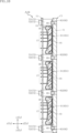
- FIG. 9 is a cross-sectional view taken along line IX-IX in FIG. FIG.
- FIG. 10 is a cross-sectional view taken along line XX in FIG.
- FIG. 11 is a cross-sectional view taken along line XI-XI in FIG.
- FIG. 12 is a cross-sectional view taken along line XII-XII in FIG.
- FIG. 13 is a cross-sectional view taken along line XIII-XIII in FIG.
- FIG. 14 is a partially enlarged cross-sectional view of the semiconductor module according to the first embodiment.
- FIG. 15 is a perspective view showing a semiconductor device of the semiconductor module according to the first embodiment.
- FIG. 16 is a plan view showing the semiconductor device of the semiconductor module according to the first embodiment.
- FIG. 17 is a plan view of FIG. 16 in which the sealing portion is shown by imaginary lines.
- FIG. 18 is a plan view of FIG.
- FIG. 19 is a front view showing the semiconductor device of the semiconductor module according to the first embodiment.
- FIG. 20 is a bottom view showing the semiconductor device of the semiconductor module according to the first embodiment.
- FIG. 21 is a cross-sectional view taken along line XXI-XXI in FIG.
- FIG. 22 is a partially enlarged cross-sectional view of FIG.
- FIG. 23 is a partially enlarged cross-sectional view of FIG.
- FIG. 24 is a cross-sectional view taken along line XXIV-XXIV in FIG.
- FIG. 25 is a cross-sectional view taken along line XXV-XXV in FIG.
- FIG. 26 is a cross-sectional view taken along line XXVI-XXVI in FIG.
- FIG. 27 is an enlarged cross-sectional view of a portion of FIG.
- FIG. 28 is a schematic diagram of a vehicle equipped with the semiconductor module according to the first embodiment.
- FIG. 29 is a partially enlarged cross-sectional view showing a semiconductor module according to a first modified example of the first embodiment, and shows a cross section similar to that of FIG.
- FIG. 30 is a partially enlarged cross-sectional view showing a semiconductor module according to a second modification of the first embodiment, and shows a cross section similar to that of FIG.
- an object A is formed on an object B
- an object A is formed on (an object B)
- an object A is formed directly on an object B
- an object A is formed on an object B with another object interposed between the object A and the object B” unless otherwise specified.
- An object A is disposed on an object B” and “an object A is disposed on (an object B)” include “an object A is disposed directly on an object B” and “an object A is disposed on (an object B) with another object interposed between the object A and the object B” unless otherwise specified.
- An object A is located on (an object B) includes “an object A is in contact with an object B and is located on (an object B)” and “an object A is located on (an object B) with another object interposed between the object A and the object B".
- an object A overlaps an object B includes “an object A overlaps the entire object B” and “an object A overlaps a part of an object B” unless otherwise specified.
- An object A (its material) contains a certain material C includes “an object A (its material) is made of a certain material C” and “an object A (its material) is mainly composed of a certain material C.”
- a certain surface A faces (one side or the other side of) direction B is not limited to the case where the angle of surface A with respect to direction B is 90°, but also includes the case where surface A is tilted with respect to direction B.
- First embodiment: 1 to 14 show a semiconductor module A10 according to the first embodiment.
- the semiconductor module A10 includes a plurality of semiconductor devices B1, a heat sink C1, a mounting member D1, and a wiring board E1.
- the thickness direction z corresponds to the thickness direction of the semiconductor module A10.
- plane view refers to the case when viewed in the thickness direction z.
- the first direction x is perpendicular to the thickness direction z.
- the second direction y is perpendicular to the thickness direction z and the first direction x.
- One side of the first direction x is referred to as the x1 side of the first direction x, and the other side of the first direction x is referred to as the x2 side of the first direction x.
- One side of the second direction y is referred to as the y1 side of the second direction y, and the other side of the second direction y is referred to as the y2 side of the second direction y.
- One side of the thickness direction z is referred to as the z1 side of the thickness direction z, and the other side of the thickness direction z is referred to as the z2 side of the thickness direction z.
- the z1 side of the thickness direction z is sometimes referred to as the upper side, and the z2 side of the thickness direction z is sometimes referred to as the lower side. Note that terms such as “top,” “bottom,” “upper,” “lower,” “top surface,” and “bottom surface” indicate the relative positional relationship of each part in the thickness direction z, and do not necessarily define the relationship with the direction of gravity.
- the multiple semiconductor devices B1 are arranged along the second direction y as shown in Figures 2, 4, 7, and 8.
- Each of the multiple semiconductor devices B1 includes multiple semiconductor elements 21.
- the multiple semiconductor elements 21 are switching elements such as MOSFETs and IGBTs, and each of the multiple semiconductor devices B1 constitutes, for example, a half-bridge type switching circuit.
- Each of the multiple semiconductor devices B1 includes multiple power terminals 13, multiple signal terminals 17, and a sealing portion 50 as shown in Figures 1 to 9. In each of the multiple semiconductor devices B1, the multiple semiconductor elements 21 are covered by the sealing portion 50.
- the multiple power terminals 13 protrude in the first direction x from the side of the sealing portion 50 (second side surface 532 described later).
- the multiple signal terminals 17 protrude in the thickness direction z from the upper surface of the sealing portion 50 (top surface 51 described later).
- the semiconductor module A10 includes three semiconductor devices B1, but may include two or four or more semiconductor devices B1.
- a first device B11 when distinguishing between the three semiconductor devices B1, they are referred to as a first device B11, a second device B12, and a third device B13.
- the first device B11 is located closest to the y1 side of the multiple semiconductor devices B1 in the second direction y.
- the third device B13 is located closest to the y2 side of the multiple semiconductor devices B1 in the second direction y.
- the second device B12 is located between the first device B11 and the third device B13 in the second direction y.
- the heat sink C1 supports the multiple semiconductor devices B1. Most of the heat sink C1 is located below the multiple semiconductor devices B1 in the thickness direction z (on the z2 side). The heat sink C1 faces the lower surface (bottom surface 52 described below) of the sealing portion 50 of the multiple semiconductor devices B1.
- the material of the heat sink C1 includes aluminum, for example. The material is not limited to aluminum, and may be other metal materials or resin materials (preferably those with good thermal conductivity).
- the heat sink C1 includes a main body portion 71, multiple pedestal portions 72, and multiple positioning portions 73.
- the main body 71 is a plate material.
- the multiple semiconductor devices B1 are mounted on the main body 71. Therefore, as shown in Figures 2, 4, 7 and 8, the multiple semiconductor devices B1 are arranged on the main body 71 along the second direction y.
- the main body 71 faces the lower surface (bottom surface 52 described below) of each sealing portion 50 of the multiple semiconductor devices B1.
- the main body 71 contacts each semiconductor device B1.
- the main body 71 is, for example, rectangular in plan view.
- each of the multiple pedestal portions 72 protrudes upward in the thickness direction z from the main body portion 71.
- the multiple pedestal portions 72 are formed integrally with the main body portion 71, but they may be attached to the main body portion 71 as separate bodies.
- Each of the multiple pedestal portions 72 includes a first portion 721 and a second portion 722, as shown in Figures 9 to 13.
- the first portion 721 is interposed between the wiring substrate E1 and the main body portion 71 in the thickness direction z.
- the dimension of the first portion 721 in the thickness direction z is greater than the dimension of the sealing portion 50 of each semiconductor device B1 in the thickness direction z.
- the second portion 722 is disposed on the first portion 721.
- the wiring substrate E1 is sandwiched between the first portion 721 and the second portion 722. With this configuration, the wiring substrate E1 is disposed at a fixed distance from the upper surface of the main body portion 71.
- the first part 721 has a concave part machined with a female thread
- the second part 722 has a convex part machined with a male thread.
- the second part 722 is fastened to the first part 721 by inserting the male thread part (convex part) of the second part 722 into the female thread part (concave part) of the first part 721.
- Each pedestal part 72 may have a structure in which the first part 721 and the second part 722 are fitted together.
- the structure may be such that the second part 722 is press-fitted into the first part 721.
- the first part 721 may have a convex part
- the second part 722 may have a concave part.
- each of the positioning parts 73 protrudes upward from the main body part 71 in the thickness direction z.
- each of the positioning parts 73 is attached to the main body part 71 as a separate body. Unlike this example, each positioning part 73 may be formed integrally with the main body part 71.
- each positioning part 73 is press-fitted into a through hole formed in the main body part 71.
- Each positioning part 73 is cylindrical and has a tapered tip on the z1 side in the thickness direction z.
- the diameter of each positioning part 73 in plan view is smaller than the diameter of each base part 72 in plan view.
- the multiple positioning parts 73 include those arranged on the y1 side of the first device B11 in the second direction y and those arranged on the y2 side of the third device B13 in the second direction y.
- the mounting member D1 holds the multiple semiconductor devices B1 to the heat sink C1.
- the mounting member D1 is, for example, a leaf spring.
- the elastic force of the mounting member D1 presses the multiple semiconductor devices B1 against the heat sink C1.
- the material of the mounting member D1 is not limited in any way, but may be, for example, copper, iron, titanium, or an alloy containing any of these (including, for example, stainless steel).
- the mounting member D1 includes multiple pressing portions 81 and multiple fixing portions 82.
- the multiple pressing portions 81 are provided individually for each of the multiple semiconductor devices B1. Each of the multiple pressing portions 81 contacts the sealing portion 50 (top surface 51) of the corresponding semiconductor device B1. Each pressing portion 81 presses the semiconductor device B1 it contacts against the main body portion 71 of the heat sink C1.
- Each of the multiple fixing parts 82 is fixed to the heat sink C1, and in this embodiment, is fixed to the main body part 71.
- Each of the multiple fixing parts 82 is, for example, a flat plate parallel to the x-y plane.
- a through hole is formed in each of the multiple fixing parts 82.
- a fastener 89 (a hexagonal bolt in the illustrated example) is inserted into the through hole. The fastener 89 fixes the fixing part 82 to the main body part 71.
- the multiple fixing parts 82 include multiple end arrangement parts 821 and multiple intermediate arrangement parts 822.
- the multiple fixing parts 82 include a pair of end arrangement parts 821 and two intermediate arrangement parts 822. As shown in Figures 4 and 10, one of the pair of end arrangement parts 821 is located on the y1 side of the first device B11 in the second direction y, and the other of the pair of end arrangement parts 821 is located on the y2 side of the third device B13 in the second direction y. One of the two intermediate arrangement parts 822 is located between the first device B11 and the second device B12, and the other of the two intermediate arrangement parts 822 is located between the second device B12 and the third device B13.
- the width (dimension in the first direction x) of each of the two end arrangement portions 821 is smaller than the width (dimension in the first direction x) of each of the pressing portions 81 and the width (dimension in the first direction x) of each of the intermediate arrangement portions 822.
- the width of the pressing portion 81 and the width of each of the intermediate arrangement portions 822 may be the same as the width of each of the two end arrangement portions 821.
- the mounting member D1 can be formed in a rectangular shape (strip shape) in a plan view.
- the width of each of the intermediate arrangement portions 822 may be the same as the width of each of the two end arrangement portions 821.
- the wiring board E1 is provided in common for the multiple semiconductor devices B1, as shown in Figures 1, 3, 7, and 8. Unlike this configuration, multiple wiring boards E1 may be provided individually for the multiple semiconductor devices B1. As can be seen from Figures 9 and 11, the signal terminals 17 of the multiple semiconductor devices B1 are inserted into the wiring board E1.
- the wiring board E1 is conductive to each signal terminal 17.
- the wiring board E1 is, for example, a drive circuit that controls the drive of each semiconductor element 21 of the multiple semiconductor devices B1. In an example in which each semiconductor element 21 is a MOSFET or IGBT, the wiring board E1 is a gate driver.
- the wiring board E1 is disposed above (on the z1 side) the sealing portions 50 of the multiple semiconductor devices B1 in the thickness direction z.
- the wiring board E1 faces the upper surfaces (top surfaces 51) of the sealing portions 50 of the multiple semiconductor devices B1.
- the wiring board E1 is located on the opposite side of the main body 71 of the heat sink C1 with respect to the multiple semiconductor devices B1. In a plan view, the wiring substrate E1 overlaps each of the sealing portions 50 of the semiconductor devices B1.
- the wiring substrate E1 is held by the multiple pedestal portions 72 at a fixed distance in the thickness direction z from the upper surfaces (top surfaces 51) of the sealing portions 50 of the semiconductor devices B1 (see FIG. 27).
- the wiring board E1 has a base material 90, a first wiring 91, a second wiring 92, a third wiring 93, and a fourth wiring 94.
- the substrate 90 has a first surface 901 and a second surface 902.
- the first surface 901 is located above (z1 side) the substrate 90 in the thickness direction z and faces the z1 side of the thickness direction z.
- the second surface 902 is located below (z2 side) the substrate 90 in the thickness direction z and faces the z2 side of the thickness direction z.
- the substrate 90 has a plurality of through holes 903 penetrating in the thickness direction z.
- the substrate 90 has a first recess 904.
- the first recess 904 is recessed from the inner surface of the through hole 903 and the second surface 902, and is formed individually in each through hole 903.
- the first recess 904 includes a portion (first portion) located radially inward of the through hole 903 as it moves toward the z1 side of the thickness direction z.
- the first recess 904 is formed in an inclined cone shape so that the entire first recess 904 is located radially inward of the through hole 903 as it moves toward the z1 side of the thickness direction z.
- the first recess 904 has a first edge 904a and a second edge 904b.
- the first edge 904a contacts the inner surface of the through hole 903.
- the second edge 904b contacts the second surface 902.
- the first recess 904. is formed by cutting concentrically with the through hole 903 from the z2 side in the thickness direction z of the substrate 90 using a drill with a conical tip.
- the first wiring 91 is disposed on the first surface 901 of the substrate 90.
- the second wiring 92 is disposed on the second surface 902.
- the third wiring 93 is disposed on the inner surface of the through hole 903 and is connected to the first wiring.
- the fourth wiring 94 is disposed in the first recess 904.
- the fourth wiring 94 is connected to both the second wiring 92 and the third wiring 93.
- the first wiring 91 forms a path for mutual conduction between the second wiring 92, the fourth wiring 94, and the third wiring 93 and the circuit provided on the wiring board E1.
- the first wiring 91, the second wiring 92, the third wiring 93, and the fourth wiring 94 are formed, for example, by metal plating formed on the surface of the substrate 90.
- the composition of the metal plating includes copper (Cu).
- Examples of dimensions of the substrate 90 include a first dimension L1, which is the length in the thickness direction z of the substrate 90, of about 1.6 mm to 3.2 mm.
- the inner diameter (diameter of the inner surface) of the through hole 903 is, for example, about 0.9 mm to 1.2 mm.
- the ratio of the second dimension L2, which is the radial length of the through hole 903 from the first edge 904a to the second edge 904b, to the thickness (first dimension L1) of the substrate 90 is, for example, 5% to 40%, preferably 9% to 15%.
- the ratio of the third dimension L3, which is the length in the thickness direction z from the first edge 904a to the second edge 904b, to the thickness (first dimension L1) of the substrate 90 is, for example, 5% to 40%, preferably 9% to 15%.
- the second dimension L2 is, for example, about 0.2 mm to 1.0 mm.
- the third dimension L3 is, for example, about 0.2 mm to 1.0 mm.
- the thickness of the first wiring 91, second wiring 92, third wiring 93 and fourth wiring 94 (metal plating) formed on the substrate 90 is, for example, approximately 10 to 18 ⁇ m.
- FIG. 14 shows the portion of the signal terminals 17 that is inserted into the through hole 903 of the substrate 90. All of the signal terminals 17 of the multiple semiconductor devices B1 are inserted into the through hole 903 of the substrate 90, as shown in FIG. 14.
- each signal terminal 17 has a base 170A and a bulge 170B.
- the z2 side of the base 170A in the thickness direction z is press-fitted into one of the multiple sleeves 64 (described later) of the multiple semiconductor devices B1.
- the outer diameter (diameter) of the base 170A is, for example, about 0.6 mm to 1.2 mm.
- the bulge 170B is provided on the z1 side of the base 170A in the thickness direction z.
- the bulge 170B bulges in a direction perpendicular to the thickness direction z from the base 170A.
- the bulge 170B has a bulge tip 170c.
- the bulge tip 170c is the part that bulges most from the base 170A in a direction perpendicular to the thickness direction z.
- the bulge tip 170c is located at the center of the thickness direction z of the bulge 170B.
- each signal terminal 17 is press-fitted into one of the multiple through holes 903 of the wiring board E1.
- the bulge 170B (bulge tip 170c) of each signal terminal 17 contacts the third wiring 93 arranged in one of the multiple through holes 903.
- the third wiring 93 arranged in one of the multiple through holes 903 is pressed against the bulge 170B (bulge tip 170c) of the signal terminal 17 inserted into the through hole 903. Therefore, each signal terminal 17 is press-fitted into the through hole 903 in the thickness direction z, and is thereby electrically connected to the wiring board E1.
- the wiring board E1 is supported by each signal terminal 17.
- the wiring board E1 has a plurality of mounting holes 951 and a plurality of positioning holes 952 formed therein.
- each mounting hole 951 is formed, for example, as a perfect circle in a plan view.
- the diameter of each mounting hole 951 in a plan view is smaller than the diameter of each base portion 72 (particularly first portion 721) in a plan view. Therefore, the wiring board E1 is held above the first portion 721 in the thickness direction z (z1 side).
- a plurality of positioning portions 73 are individually inserted into each of the positioning holes 952.
- two positioning holes 952 are formed in the wiring board E1.
- One of the two positioning holes 952 (the positioning hole 952 arranged on the y1 side of the second direction y) is formed as a perfect circle, and the other of the two positioning holes 952 (the positioning hole 952 arranged on the y2 side of the second direction y) is formed as an elongated hole.
- by forming one of the two positioning holes 952 as an elongated hole it is possible to suppress misalignment of the heat sink C1 and the wiring board E1 due to manufacturing errors.
- Figures 15 to 26 are enlarged views of one of the multiple semiconductor devices B1.
- the multiple semiconductor devices B1 all have the same structure. Unless otherwise specified, the semiconductor device B1 described below is common to the first device B11, the second device B12, and the third device B13.
- each semiconductor device B1 (first device B11, second device B12, and third device B13) includes the above-mentioned power terminals 13, signal terminals 17, semiconductor elements 21, and sealing portion 50, as well as a support substrate 11, a pair of thermistors 22, a first conductive member 31, a second conductive member 32, wires, and a pair of control wiring 60.
- the power terminals 13 include a first power terminal 14, two second power terminals 15, and two third power terminals 16, and the signal terminals 17 include a first signal terminal 171, a second signal terminal 172, a third signal terminal 173, a fourth signal terminal 174, a pair of fifth signal terminals 181, and a pair of sixth signal terminals 182.
- the wires include a first wire 41, a second wire 42, a third wire 43, and a fourth wire 44.
- Each semiconductor device B1 converts the DC power supply voltage applied to the first power terminal 14 and the two second power terminals 15 into AC power using multiple semiconductor elements 21.
- the converted AC power is input from the two third power terminals 16 to a power supply target such as a motor.
- the support substrate 11 supports a plurality of semiconductor elements 21 in the thickness direction z.
- the support substrate 11 is composed of, for example, a DBC (Direct Bonded Copper) substrate.
- the support substrate 11 includes an insulating layer 111, a first wiring layer 112, and a second wiring layer 113.
- the support substrate 11 is covered by a sealing portion 50 except for a portion of the second wiring layer 113.
- the insulating layer 111 includes a portion that is interposed between the first wiring layer 112 and the second wiring layer 113 in the thickness direction z.
- the insulating layer 111 is made of a material with relatively high thermal conductivity.
- the insulating layer 111 is made of ceramics containing aluminum nitride (AlN), for example.
- the insulating layer 111 may be made of an insulating resin sheet in addition to ceramics.
- the first wiring layer 112 is located above (on the z1 side) the insulating layer 111 in the thickness direction z.
- the composition of the first wiring layer 112 includes copper (Cu).
- the first wiring layer 112 is surrounded by the periphery of the insulating layer 111 in a planar view.
- the first wiring layer 112 includes a first mounting portion 1121 and a second mounting portion 1122.
- the first mounting portion 1121 and the second mounting portion 1122 are each rectangular in a planar view.
- the first mounting portion 1121 and the second mounting portion 1122 are separated from each other in the first direction x.
- the first mounting portion 1121 is located on the x1 side of the second mounting portion 1122 in the first direction x.
- Each of the multiple semiconductor elements 21 is bonded to either the first mounting portion 1121 or the second mounting portion 1122.
- the second wiring layer 113 is located below (on the z2 side) the insulating layer 111 in the thickness direction z. As shown in Figure 20, the second wiring layer 113 is exposed from the sealing portion 50.
- the lower surface of the second wiring layer 113 corresponds to the bottom surface of the support substrate 11.
- the lower surface of the second wiring layer 113 (the bottom surface of the support substrate 11) is in contact with the upper surface of the body portion 71 of the heat sink C1 (the surface facing the z1 side in the thickness direction z).
- the composition of the second wiring layer 113 includes copper.
- the second wiring layer 113 is rectangular in plan view.
- the second wiring layer 113 is surrounded by the periphery of the insulating layer 111 in plan view.
- each of the multiple semiconductor elements 21 is mounted on either the first mounting portion 1121 or the second mounting portion 1122.
- Each semiconductor element 21 is, for example, a MOSFET.
- each semiconductor element 21 may be a switching element such as an IGBT or a diode.
- the semiconductor element 21 is an n-channel type MOSFET with a vertical structure.
- the semiconductor element 21 includes a compound semiconductor substrate.
- the composition of the compound semiconductor substrate includes silicon carbide (SiC) or silicon (Si).
- the multiple semiconductor elements 21 include multiple first elements 21A and multiple second elements 21B.
- the structure of each of the multiple second elements 21B is the same as the structure of each of the multiple first elements 21A.
- the multiple first elements 21A are mounted on a first mounting portion 1121.
- the multiple first elements 21A are arranged along the second direction y.
- the multiple second elements 21B are mounted on a second mounting portion 1122.
- the multiple second elements 21B are arranged along the second direction y.
- the multiple semiconductor elements 21 have a first electrode 211, a second electrode 212, a third electrode 213 and two fourth electrodes 214.
- the first electrode 211 faces either the first mounting portion 1121 or the second mounting portion 1122. A current corresponding to the power before being converted by the semiconductor element 21 flows through the first electrode 211. In other words, the first electrode 211 corresponds to the drain electrode of the semiconductor element 21.
- the second electrode 212 is located on the opposite side to the first electrode 211 in the thickness direction z. A current corresponding to the power converted by the semiconductor element 21 flows through the second electrode 212. In other words, the second electrode 212 corresponds to the source electrode of the semiconductor element 21.
- the third electrode 213 is located on the same side as the second electrode 212 in the thickness direction z.
- a drive signal (gate voltage) for driving the semiconductor element 21 is input to the third electrode 213.
- the third electrode 213 corresponds to the gate electrode of the semiconductor element 21.
- the area of the third electrode 213 is smaller than the area of the second electrode 212 in a plan view.
- the two fourth electrodes 214 are located on the same side as the second electrode 212 in the thickness direction z, and are located next to the third electrode 213 in the first direction x.
- the two fourth electrodes 214 are arranged on either side of the third electrode 213 in the first direction x, sandwiching the third electrode 213 therebetween.
- the potential of each fourth electrode 214 is equal to the potential of the second electrode 212.
- each semiconductor element 21 may include only one of the two fourth electrodes 214, or may not include either of the two fourth electrodes 214.
- the conductive bonding layer 23 is interposed between either the first mounting portion 1121 or the second mounting portion 1122 and the first electrode 211 of any of the multiple semiconductor elements 21.
- the conductive bonding layer 23 is, for example, solder.
- the conductive bonding layer 23 may include a sintered body of metal particles.
- the first electrodes 211 of the multiple first elements 21A are conductively bonded to the first mounting portion 1121 via the conductive bonding layer 23.
- each of the first electrodes 211 of the multiple first elements 21A is electrically connected to the first mounting portion 1121.
- the first electrodes 211 of the multiple second elements 21B are conductively bonded to the second mounting portion 1122 via the conductive bonding layer 23.
- each of the first electrodes 211 of the multiple second elements 21B is electrically connected to the second mounting portion 1122.
- the multiple power terminals 13 are each electrically connected to the multiple semiconductor elements 21. A current corresponding to the power before being converted by the multiple semiconductor elements 21 or a current corresponding to the power after being converted by the multiple semiconductor elements 21 flows through the multiple power terminals 13.
- the multiple power terminals 13 include a first power terminal 14, two second power terminals 15, and two third power terminals 16.
- the first power terminal 14 is joined to the first mounting portion 1121 as shown in FIG. 18 and FIG. 24. This joining is not limited in any way and may be joining with a conductive joining material (for example, solder) not shown, joining by laser welding, or crimping joining.
- the first power terminal 14 is electrically connected to the first electrodes 211 of the multiple first elements 21A via the first mounting portion 1121.
- the first power terminal 14 is a P terminal (positive electrode) to which a DC power supply voltage to be the subject of power conversion is applied. As shown in FIG. 18, the first power terminal 14 is located on the opposite side of the second mounting portion 1122 in the first direction x, sandwiching the first mounting portion 1121 therebetween.
- the first power terminal 14 extends from the first mounting portion 1121 to one side (x1 side) of the first direction x, and protrudes from the sealing portion 50 to one side (x1 side) of the first direction x. As shown in FIG. 17 and FIG. 24, the first power terminal 14 includes a portion covered by the sealing portion 50 and a portion exposed from the sealing portion 50. In the first power terminal 14, the portion covered by the sealing portion 50 is joined to the first mounting portion 1121. In the first power terminal 14, the portion exposed from the sealing portion 50 is used as the aforementioned P terminal of each semiconductor device B1.
- a second conductive member 32 is joined to the two second power terminals 15.
- the two second power terminals 15 are electrically connected to the second electrodes 212 of the multiple second elements 21B via the second conductive member 32.
- the two second power terminals 15 are N terminals (negative electrodes) to which the DC power supply voltage to be the subject of power conversion is applied.
- the two second power terminals 15 are spaced apart from each other in the second direction y.
- the first power terminal 14 is located between the two second power terminals 15. As shown in FIG. 18, the two second power terminals 15 are each located on the same side as the first power terminal 14 with respect to the first mounting portion 1121 and the second mounting portion 1122 in the first direction x.
- the two second power terminals 15 are each spaced apart from the first mounting portion 1121 and the second mounting portion 1122. Each of the two second power terminals 15 extends in the first direction x and protrudes from the sealing portion 50 to one side (x1 side) in the first direction x. As shown in FIG. 17 and FIG. 21, each of the two second power terminals 15 includes a portion covered by the sealing portion 50 and a portion exposed from the sealing portion 50. In each of the second power terminals 15, the second conductive member 32 is joined to the portion covered by the sealing portion 50. In each of the second power terminals 15, the portion exposed from the sealing portion 50 is used as the aforementioned N terminal of each of the semiconductor devices B1.
- the two third power terminals 16 are each joined to the second mounting portion 1122 as shown in FIG. 18 and FIG. 21. This joining is not limited in any way and may be joining with a conductive joining material (for example, solder) not shown, joining by laser welding, or crimping joining.
- the two third power terminals 16 are each electrically connected to the first electrodes 211 of the multiple second elements 21B via the second mounting portion 1122.
- the two third power terminals 16 are each electrically connected to the second electrodes 212 of the multiple first elements 21A via the second mounting portion 1122 and the first conductive member 31. AC power converted by the multiple semiconductor elements 21 (the multiple first elements 21A and the multiple second elements 21B) is output from the two third power terminals 16.
- the two third power terminals 16 are each an output terminal of the AC power.
- the two third power terminals 16 are separated from each other in the second direction y.
- the two third power terminals 16 are located on the opposite side of the first mounting portion 1121 in the first direction x, with the second mounting portion 1122 sandwiched therebetween.
- the two third power terminals 16 each extend from the second mounting portion 1122 to the other side (x2 side) of the first direction x, and protrude from the sealing portion 50 to the other side (x2 side) of the first direction x.
- the two third power terminals 16 each include a portion covered by the sealing portion 50 and a portion exposed from the sealing portion 50. In each of the third power terminals 16, the portion covered by the sealing portion 50 is joined to the second mounting portion 1122. In each of the third power terminals 16, the portion exposed from the sealing portion 50 is used as the output terminal described above for each semiconductor device B1.
- the pair of control wirings 60 constitute a part of the conductive path between the plurality of signal terminals 17 and the plurality of semiconductor elements 21.
- the pair of control wirings 60 includes a first wiring 601 and a second wiring 602.
- the first wiring 601 is located between the plurality of first elements 21A and the first power terminal 14 and the two second power terminals 15 in the first direction x.
- the first wiring 601 is joined to the first mounting portion 1121 as shown in FIG. 18 and FIG. 24.
- the second wiring 602 is located between the plurality of second elements 21B and the two third power terminals 16 in the first direction x.
- the second wiring 602 is joined to the second mounting portion 1122 as shown in FIG. 18 and FIG. 24.
- the pair of control wirings 60 has an insulating layer 61, a plurality of wiring layers 62, a metal layer 63 and a plurality of sleeves 64.
- the pair of control wirings 60 are covered by the sealing portion 50 except for a portion of each of the multiple sleeves 64.
- the insulating layer 61, multiple wiring layers 62, metal layer 63, and multiple sleeves 64 described below are common to the pair of control wirings 60 (first wiring 601 and second wiring 602) unless otherwise specified.
- the insulating layer 61 includes a portion interposed between the multiple wiring layers 62 and the metal layer 63 in the thickness direction z.
- the insulating layer 61 is made of, for example, ceramics.
- the insulating layer 61 may be made of an insulating resin sheet in addition to ceramics.
- the multiple wiring layers 62 are located above (on the z1 side of) the insulating layer 61 in the thickness direction z.
- the composition of the multiple wiring layers 62 includes copper.
- the multiple wiring layers 62 include a first wiring layer 621, a second wiring layer 622, a third wiring layer 623, a fourth wiring layer 624, and a fifth wiring layer 625.
- the metal layer 63 is located on the opposite side to the multiple wiring layers 62 in the thickness direction z, with the insulating layer 61 sandwiched therebetween.
- the metal layer 63 contains copper.
- the metal layer 63 of the first wiring 601 is bonded to the first mounting portion 1121 by an adhesive layer (not shown).
- the metal layer 63 of the second wiring 602 is bonded to the second mounting portion 1122 by an adhesive layer (not shown).
- These adhesive layers are made of materials that may or may not be conductive. For example, these adhesive layers are solder.
- the multiple sleeves 64 are respectively bonded to the multiple wiring layers 62. This bonding is performed by a conductive bonding layer (e.g., solder) not shown.
- the multiple sleeves 64 are made of a conductive material such as metal.
- Each of the multiple sleeves 64 is tubular and extends along the thickness direction z.
- One end of the multiple sleeves 64 (the edge on the z2 side in the thickness direction z) is conductively bonded to one of the multiple wiring layers 62.
- the other end of the multiple sleeves 64 (the edge on the z1 side in the thickness direction z) is exposed from the sealing portion 50.
- one of the pair of thermistors 22 straddles and is conductively joined to a pair of third wiring layers 623 of the first wiring 601.
- the other of the pair of thermistors 22 straddles and is conductively joined to a pair of third wiring layers 623 of the second wiring 602.
- Each of the pair of thermistors 22 is, for example, an NTC (Negative Temperature Coefficient) thermistor. NTC thermistors have the property that their resistance decreases gradually as the temperature increases.
- NTC thermistors 22 is used as a temperature detection sensor for the semiconductor device B1.
- each of the multiple signal terminals 17 consists of a metal pin extending in the thickness direction z.
- the multiple signal terminals 17 protrude from a top surface 51 (described later) of the sealing portion 50.
- the multiple signal terminals 17 are individually pressed into the multiple sleeves 64 of the pair of control wirings 60.
- each of the multiple signal terminals 17 is supported by one of the multiple sleeves 64 and is conductive to one of the multiple wiring layers 62.
- the multiple signal terminals 17 include a first signal terminal 171, a second signal terminal 172, a third signal terminal 173, a fourth signal terminal 174, a pair of fifth signal terminals 181, a pair of sixth signal terminals 182, and a seventh signal terminal 19.
- the first signal terminal 171, the second signal terminal 172, the third signal terminal 173, the fourth signal terminal 174, the pair of fifth signal terminals 181, the pair of sixth signal terminals 182, and the seventh signal terminal 19 are inserted into the wiring board E1 and input or output each signal to the wiring board E1.
- the first signal terminal 171 is press-fitted into one of the multiple sleeves 64 that is joined to the first wiring layer 621 of the first wiring 601. As a result, the first signal terminal 171 is supported by the sleeve 64 and is conductive to the first wiring layer 621 of the first wiring 601. Furthermore, the first signal terminal 171 is conductive to the third electrodes 213 of the multiple first elements 21A. A gate voltage is applied to the first signal terminal 171 to drive the multiple first elements 21A.
- the second signal terminal 172 is press-fitted into one of the multiple sleeves 64 that is joined to the first wiring layer 621 of the second wiring 602. As a result, the second signal terminal 172 is supported by the sleeve 64 and is conductive to the first wiring layer 621 of the second wiring 602. Furthermore, the second signal terminal 172 is conductive to the third electrodes 213 of the multiple second elements 21B. A gate voltage is applied to the second signal terminal 172 to drive the multiple second elements 21B.
- the third signal terminal 173 is located next to the first signal terminal 171 in the second direction y.
- the third signal terminal 173 is press-fitted into one of the multiple sleeves 64 that is joined to the second wiring layer 622 of the first wiring 601.
- the third signal terminal 173 is supported by the sleeve 64 and is conductive to the second wiring layer 622 of the first wiring 601.
- the third signal terminal 173 is conductive to the fourth electrodes 214 of the multiple first elements 21A.
- a voltage corresponding to the maximum current among the currents flowing through the fourth electrodes 214 of the multiple first elements 21A is applied to the third signal terminal 173.
- the fourth signal terminal 174 is located next to the second signal terminal 172 in the second direction y.
- the fourth signal terminal 174 is press-fitted into one of the multiple sleeves 64 that is joined to the second wiring layer 622 of the second wiring 602.
- the fourth signal terminal 174 is supported by the sleeve 64 and is conductive to the second wiring layer 622 of the second wiring 602.
- the fourth signal terminal 174 is conductive to the fourth electrodes 214 of the multiple second elements 21B.
- a voltage corresponding to the maximum current among the currents flowing through the fourth electrodes 214 of the multiple second elements 21B is applied to the fourth signal terminal 174.
- the pair of fifth signal terminals 181 are located on the opposite side of the first signal terminal 171 from the third signal terminal 173 in the second direction y.
- the pair of fifth signal terminals 181 are adjacent to each other in the second direction y.
- the pair of fifth signal terminals 181 are individually press-fitted into a pair of sleeves 64 respectively joined to a pair of third wiring layers 623 of the first wiring 601.
- the pair of fifth signal terminals 181 are individually supported by the pair of sleeves 64 and are individually conductive to the pair of third wiring layers 623 of the first wiring 601.
- the pair of fifth signal terminals 181 are conductive to the thermistor 22 on the first wiring 601.
- the pair of sixth signal terminals 182 are located on the opposite side of the second signal terminal 172 from the fourth signal terminal 174 in the second direction y.
- the pair of sixth signal terminals 182 are adjacent to each other in the second direction y.
- the pair of sixth signal terminals 182 are individually press-fitted into a pair of sleeves 64 respectively joined to a pair of third wiring layers 623 of the second wiring 602.
- the pair of sixth signal terminals 182 are individually supported by the pair of sleeves 64 and are individually conductive to the pair of third wiring layers 623 of the second wiring 602.
- the pair of sixth signal terminals 182 are conductive to the thermistor 22 on the second wiring 602.
- the seventh signal terminal 19 is located on the opposite side of the first signal terminal 171 in the second direction y, with the third signal terminal 173 sandwiched therebetween.
- the seventh signal terminal 19 is press-fitted into a sleeve 64 joined to the fifth wiring layer 625 of the first wiring 601.
- the seventh signal terminal 19 is supported by the sleeve 64 and is conductive to the fifth wiring layer 625 of the first wiring 601.
- the seventh signal terminal 19 is conductive to the first mounting portion 1121.
- a voltage equivalent to the DC power input to the first power terminal 14 is applied to the seventh signal terminal 19.
- the multiple first wires 41, the multiple second wires 42, the multiple third wires 43, and the fourth wires 44 each electrically connect parts spaced apart from one another.
- the multiple first wires 41, the multiple second wires 42, the multiple third wires 43, and the fourth wires 44 are each bonding wires. Note that the multiple first wires 41, the multiple second wires 42, the multiple third wires 43, and the fourth wires 44 are omitted in Figures 17 and 21 to 24.
- the first wires 41 include first wires 41 conductively joined to the third electrodes 213 of the first elements 21A and the fourth wiring layer 624 of the first wiring 601, as shown in FIG. 18.
- the third wires 43 include third wires 43 conductively joined to the fourth wiring layer 624 of the first wiring 601 and the first wiring layer 621 of the first wiring 601, as shown in FIG. 18.
- the first signal terminal 171 is conductive to the third electrodes 213 of the first elements 21A.
- the composition of the first wires 41 and the third wires 43 includes gold (Au).
- the composition of the first wires 41 and the third wires 43 may include copper or aluminum.
- the plurality of first wires 41 include first wires 41 conductively joined to the third electrodes 213 of the plurality of second elements 21B and the fourth wiring layer 624 of the second wiring 602 as shown in FIG. 18.
- the plurality of third wires 43 include third wires 43 conductively joined to the fourth wiring layer 624 of the second wiring 602 and the first wiring layer 621 of the second wiring 602 as shown in FIG. 18.
- the second signal terminal 172 is electrically connected to the third electrodes 213 of the plurality of second elements 21B.
- the second wires 42 include second wires 42 conductively bonded to one of the two fourth electrodes 214 of the first elements 21A and the second wiring layer 622 of the first wiring 601, as shown in FIG. 18.
- the third signal terminal 173 is electrically connected to one of the two fourth electrodes 214 of the first elements 21A.
- the second wires 42 include second wires 42 conductively bonded to one of the two fourth electrodes 214 of the second elements 21B and the second wiring layer 622 of the second wiring 602, as shown in FIG. 18.
- the fourth signal terminal 174 is electrically connected to one of the two fourth electrodes 214 of the second elements 21B.
- the composition of the second wires 42 includes gold.
- composition of the second wires 42 may include copper or aluminum.
- each semiconductor element 21 each of the multiple first elements 21A and the multiple second elements 21B
- the multiple second wires 42 are bonded one by one to each of the multiple semiconductor elements 21's second electrodes 212.
- the fourth wire 44 is conductively joined to the fifth wiring layer 625 of the first wiring 601 and the first mounting portion 1121.
- the seventh signal terminal 19 is electrically connected to the first electrodes 211 of the multiple first elements 21A via the first mounting portion 1121.
- the composition of the fourth wire 44 includes gold.
- the composition of the fourth wire 44 may include copper or aluminum.
- the first conductive member 31 is conductively joined to the second electrodes 212 of the multiple first elements 21A and the second mounting portion 1122. As a result, the second electrodes 212 of the multiple first elements 21A are electrically connected to the second mounting portion 1122.
- the composition of the first conductive member 31 includes copper.
- the first conductive member 31 is a metal clip. As shown in Figures 18 and 21, the first conductive member 31 has a main body portion 311, multiple first joints 312, and multiple second joints 313.
- the main body 311 forms a major part of the first conductive member 31. As shown in FIG. 18, the main body 311 extends in the first direction x. As shown in FIG. 18 and FIG. 21, the main body 311 straddles between the first mounting portion 1121 and the second mounting portion 1122. In the example shown in FIG. 18, a plurality of through holes are formed in the main body 311. Each of the plurality of through holes penetrates the main body 311 in the thickness direction z. The plurality of through holes overlap between the first mounting portion 1121 and the second mounting portion 1122 in a plan view. This allows the sealing portion 50 to flow smoothly downward in the thickness direction z of the main body 311 (to the z2 side of the thickness direction z) when the sealing portion 50 is formed.
- the first joints 312 are individually joined to the second electrodes 212 of the first elements 21A.
- Each of the first joints 312 faces one of the second electrodes 212 of the first elements 21A.
- each of the first joints 312 extends from the main body 311 to the x1 side in the first direction x.
- the first joints 312 are bifurcated from the main body 311, but they do not need to be bifurcated.
- the base end (the end connected to the main body 311) of each of the first joints 312 is bent downward in the thickness direction z (to the z2 side in the thickness direction z). Therefore, the tip (the end opposite to the end connected to the main body 311) of each of the first joints 312 is located downward in the thickness direction z (to the z2 side in the thickness direction z) from the main body 311 in the thickness direction z.
- each second joint 313 extends from the main body 311 to the x2 side in the first direction x.
- the base end (the end connected to the main body 311) of each second joint 313 is bent downward in the thickness direction z (to the z2 side in the thickness direction z). Therefore, the tip (the end opposite to the side connected to the main body 311) of each second joint 313 is located downward in the thickness direction z (to the z2 side in the thickness direction z) from the main body 311 in the thickness direction z.
- the semiconductor device B1 further includes a plurality of first conductive bonding layers 33.
- the plurality of first conductive bonding layers 33 are respectively interposed between the second electrodes 212 of the plurality of first elements 21A and the plurality of first bonding portions 312.
- the first conductive bonding layer 33 conductively bonds the second electrodes 212 of the plurality of first elements 21A to the plurality of first bonding portions 312.
- the first conductive bonding layer 33 is, for example, solder.
- the first conductive bonding layer 33 may include a sintered body of metal particles.
- the semiconductor device B1 further includes a plurality of second conductive bonding layers 34.
- the plurality of second conductive bonding layers 34 are respectively interposed between the second mounting portion 1122 and the plurality of second bonding portions 313.
- the second conductive bonding layer 34 conductively bonds the second mounting portion 1122 and the plurality of second bonding portions 313.
- the second conductive bonding layer 34 is, for example, solder.
- the second conductive bonding layer 34 may include a sintered body of metal particles.
- the second conductive member 32 is conductively joined to the second electrodes 212 of the multiple second elements 21B and the two second power terminals 15. As a result, the second electrodes 212 of the multiple second elements 21B are electrically connected to the two second power terminals 15.
- the composition of the second conductive member 32 includes copper.
- the second conductive member 32 is a metal clip. As shown in FIG. 17 and FIG. 21 to FIG. 26, the second conductive member 32 includes a main body portion 321, multiple third joint portions 322, and a pair of fourth joint portions 323.
- the main body 321 forms the main part of the second conductive member 32. As shown in Figures 21 and 25, the main body 321 is disposed parallel to the upper surface of the first mounting portion 1121 and the upper surface of the second mounting portion 1122. The main body 321 is separated from the main body 311 of the first conductive member 31, and is also separated from the first mounting portion 1121 and the second mounting portion 1122.
- the third joints 322 are individually joined to the second electrodes 212 of the second elements 21B.
- Each of the third joints 322 faces one of the second electrodes 212 of the second elements 21B.
- the third joints 322 extend in the first direction x from the main body 321.
- the base end (the end connected to the main body 321) of each third joint 322 is bent downward in the thickness direction z (toward the z2 side of the thickness direction z). Therefore, the tip (the end opposite to the end connected to the main body 321) of each third joint 322 is located downward in the thickness direction z (toward the z2 side of the thickness direction z) from the main body 321 in the thickness direction z.
- the pair of fourth joints 323 are individually joined to the two second power terminals 15. Each of the pair of fourth joints 323 faces a corresponding one of the two second power terminals 15.
- the semiconductor device B1 further includes a plurality of third conductive bonding layers 35.
- the plurality of third conductive bonding layers 35 are respectively interposed between the second electrodes 212 of the plurality of second elements 21B and the plurality of third bonding portions 322.
- the plurality of third conductive bonding layers 35 conductively bond the second electrodes 212 of the plurality of second elements 21B to the plurality of third bonding portions 322.
- the third conductive bonding layer 35 is, for example, solder.
- the third conductive bonding layer 35 may include a sintered body of metal particles.
- the semiconductor device B1 further includes two fourth conductive bonding layers 36.
- the two fourth conductive bonding layers 36 are respectively interposed between the two second power terminals 15 and the pair of fourth bonding portions 323.
- the two fourth conductive bonding layers 36 conductively bond the two second power terminals 15 and the pair of fourth bonding portions 323.
- the fourth conductive bonding layer 36 is, for example, solder.
- the fourth conductive bonding layer 36 may include a sintered body of metal particles.
- the sealing portion 50 covers the semiconductor elements 21, the first conductive member 31, the second conductive member 32, the first wires 41, the second wires 42, the third wires 43, and the fourth wires 44. Furthermore, the sealing portion 50 covers the support substrate 11, a portion of each of the power terminals 13, and a portion of each of the signal terminals 17.
- the sealing portion 50 has electrical insulation properties.
- the sealing portion 50 contains, for example, a black epoxy resin.
- the sealing portion 50 is formed, for example, by molding. As shown in Figures 15 to 17 and Figures 19 to 26, the sealing portion 50 has a top surface 51, a bottom surface 52, a plurality of resin side surfaces 53, and a pair of recesses 55.
- the top surface 51 faces in the same direction (z1 side in the thickness direction z) as the upper surfaces of the first mounting portion 1121 and the second mounting portion 1122 in the thickness direction z.
- the top surface 51 of each semiconductor device B1 contacts the mounting member D1.
- the wiring board E1 is positioned at a fixed distance from the top surface 51 of the sealing portion 50 of each semiconductor device B1.
- the fourth dimension L4, which is the length in the thickness direction z from the top surface 51 of the sealing portion 50 to the bulging tip portion 170c of the signal terminal 17, is, for example, approximately 5 mm to 15 mm.
- the bottom surface 52 faces the opposite side to the top surface 51 in the thickness direction z (the z2 side in the thickness direction z).
- the second wiring layer 113 of the support substrate 11 is exposed from the bottom surface 52.
- the bottom surface 52 of each semiconductor device B1 contacts the main body portion 71 of the heat sink C1.
- the multiple resin side surfaces 53 are each connected to the top surface 51.
- the multiple resin side surfaces 53 include a pair of first side surfaces 531 and a pair of second side surfaces 532.
- the pair of first side surfaces 531 are positioned apart from each other in the first direction x.
- the pair of first side surfaces 531 face opposite each other in the first direction x and extend in the second direction y.
- the pair of first side surfaces 531 are connected to the top surface 51.
- a first power terminal 14 and two second power terminals 15 each protrude from the first side surface 531 on the x1 side in the first direction x of the pair of first side surfaces 531.
- Two third power terminals 16 each protrude from the first side surface 531 on the x2 side in the first direction x of the pair of first side surfaces 531.
- the pair of second side surfaces 532 are positioned apart from each other in the second direction y.
- the pair of second side surfaces 532 face opposite each other in the second direction y and extend in the first direction x.
- the pair of second side surfaces 532 are connected to the top surface 51 and the bottom surface 52.
- the pair of recesses 55 are recessed in the first direction x from the first side surface 531 on the x1 side of the pair of first side surfaces 531 in the first direction x.
- the pair of recesses 55 extend from the top surface 51 to the bottom surface 52 in the thickness direction z.
- the pair of recesses 55 are located on both sides of the first power terminal 14 in the second direction y.
- the specific configuration of the semiconductor device B1 described above is an example and is not limited to the above example.
- the number of the signal terminals 17, or the signals input/output to/from each signal terminal 17, the number of the semiconductor elements 21, the configuration of the first wiring 601 and the second wiring 602, etc. can be changed as appropriate.
- the support substrate 11 may have a conductive plate-like member bonded onto the first wiring layer 112 (each of the first mounting portion 1121 and the second mounting portion 1122). In this case, the conductive plate-like member mounts the semiconductor elements 21 (each of the first elements 21A and the second elements 21B) and a pair of control wirings 60, etc.
- FIG. 28 is a schematic diagram of a vehicle F1 equipped with a semiconductor module A10.
- the vehicle F1 is, for example, an electric vehicle (EV).
- EV electric vehicle
- the vehicle F1 is equipped with an on-board charger 96, a storage battery 97, and a drive system 98.
- the on-board charger 96 is supplied with power wirelessly from a power supply facility (not shown) installed outdoors. Alternatively, the means for supplying power from the power supply facility to the on-board charger 96 may be wired.
- the on-board charger 96 is configured with a step-up DC-DC converter. The voltage of the power supplied to the on-board charger 96 is stepped up by the converter and then supplied to the storage battery 97. The stepped-up voltage is, for example, 600V.
- the drive system 98 drives the vehicle F1.
- the drive system 98 has an inverter 981 and a drive source 982.
- the semiconductor module A10 semiconductor device B1 constitutes part of the inverter 981.
- the power stored in the storage battery 97 is supplied to the inverter 981.
- the power supplied from the storage battery 97 to the inverter 981 is DC power.
- a step-up DC-DC converter may be further provided between the storage battery 97 and the inverter 981.
- the inverter 981 converts DC power into AC power.
- the inverter 981 including the semiconductor device B1 is conductive to the drive source 982.
- the drive source 982 has an AC motor and a transmission.
- the AC motor rotates and the rotation is transmitted to the transmission.
- the transmission appropriately reduces the rotation speed transmitted from the AC motor and then rotates the drive shaft of the vehicle F1. This drives the vehicle F1.
- the semiconductor device B1 in the inverter 981 is necessary to output AC power whose frequency has been appropriately changed to correspond to the required rotation speed of the AC motor.
- the functions and effects of the semiconductor module A10 are as follows:
- the base material 90 of the wiring board E1 has a first recess 904.
- the first recess 904 is recessed from the inner surface of the through hole 903 and the second surface 902 facing downward (z2 side) in the thickness direction z in the base material 90.
- the bulging portion 170B of the signal terminal 17 contacts the third wiring 93 arranged on the inner surface of the through hole 903.
- the first recess 904 includes a portion (first portion) that is positioned radially inward of the through hole 903 as it moves toward the z1 side in the thickness direction z.
- the first recess 904 is formed into an inclined cone shape so that the entire first recess 904 is positioned radially inward of the through hole 903 as it moves toward the z1 side in the thickness direction z.
- the signal terminal 17 (base 170A) is displaced in a direction perpendicular to the thickness direction z between the wiring board E1 and the top surface 51 of the sealing portion 50. If the thickness (first dimension L1) of the substrate 90 becomes large, the opening end of the substrate 90 on the lower side (z2 side) in the thickness direction z and the signal terminal 17 may come into contact, causing stress.
- the first recess 904 is connected to the lower side (z2 side) of the through hole 903 in the thickness direction z, and the opening end of the substrate 90 on the lower side (z2 side) in the thickness direction z is larger than the diameter of the through hole 903.
- the ratio of the second dimension L2, which is the radial length of the through hole 903 from the first edge 904a to the second edge 904b of the first recess 904, to the thickness (first dimension L1) of the substrate 90 is 5% to 40%.
- the ratio of the third dimension L3, which is the length in the thickness direction z from the first edge 904a to the second edge 904b, to the thickness (first dimension L1) of the base material 90 is, for example, 5% to 40%.
- FIGS. 29 and 30 show modified examples of the semiconductor module of the present disclosure.
- elements that are the same as or similar to those in the above embodiment are given the same reference numerals as in the above embodiment, and duplicated explanations will be omitted.
- the configurations of each part in each modified example and each embodiment can be combined with each other as appropriate to the extent that no technical contradictions arise.
- Fig. 29 shows a first modified example of the semiconductor module A10.
- Fig. 29 is a partially enlarged cross-sectional view showing a semiconductor module A11 according to the first modified example, and shows a cross section similar to that of Fig. 14.
- the semiconductor module A11 of this modified example differs from the semiconductor module A10 in the configuration of a first recess 904 in the base material 90.
- the first recess 904 includes a first portion 9041 and a second portion 9042.
- the first portion 9041 is cone-shaped and inclined so as to be positioned radially inward of the through-hole 903 as it approaches the z1 side in the thickness direction z.
- the first portion 9041 has a first edge 904a that contacts the inner surface of the through-hole 903.
- the second portion 9042 is cylindrical along the thickness direction z and connects to the z2 side in the thickness direction z relative to the first portion 9041.
- the second portion 9042 has a second edge 904b that contacts the second surface 902.
- the base material 90 of the wiring board E1 also has a first recess 904.
- the first recess 904 is recessed from the inner surface of the through hole 903 and the second surface 902 facing downward (z2 side) in the thickness direction z in the base material 90.
- the bulging portion 170B of the signal terminal 17 contacts the third wiring 93 arranged on the inner surface of the through hole 903.
- the semiconductor module A11 has the same effects as the semiconductor module A10 of the above embodiment.
- Fig. 30 shows a second modified example of the semiconductor module A10.
- Fig. 30 is a partially enlarged cross-sectional view showing a semiconductor module A12 according to the second modified example, and shows a cross section similar to that of Fig. 14.
- the semiconductor module A12 of this modified example differs from the semiconductor module A10 in the configuration of the first recess 904 in the base material 90.
- the first recess 904 includes a portion (first portion) that is located radially inward of the through hole 903 as it moves toward the z1 side in the thickness direction z.
- the first recess 904 is entirely spherical and is located radially inward of the through hole 903 as it moves toward the z1 side in the thickness direction z.
- the base material 90 of the wiring board E1 also has a first recess 904.
- the first recess 904 is recessed from the inner surface of the through hole 903 and the second surface 902 facing downward (z2 side) in the thickness direction z in the base material 90.
- the bulging portion 170B of the signal terminal 17 contacts the third wiring 93 arranged on the inner surface of the through hole 903.
- the semiconductor module A12 has the same effects as the semiconductor module A10 of the above embodiment.
- the semiconductor module according to the present disclosure is not limited to the above-described embodiment.
- the specific configuration of each part of the semiconductor module according to the present disclosure can be freely designed in various ways.
- Appendix 1 a semiconductor device including a semiconductor element, a sealing portion covering the semiconductor element, and a signal terminal protruding from the sealing portion to one side in a thickness direction of the sealing portion and electrically connected to the semiconductor element; a wiring board disposed on one side of the sealing portion in the thickness direction, the wiring board includes a base material, a first wiring, a second wiring, a third wiring, and a fourth wiring; the base material has a first surface facing one side in the thickness direction, a second surface facing the other side in the thickness direction, at least one through hole penetrating in the thickness direction, and a first recess recessed from an inner surface of the through hole and the second surface; The first wiring is disposed on the first surface, the second wiring is disposed on the second surface, the third wiring is disposed on the inner surface of the through hole, the fourth wiring is disposed in the first recess and is connected to both the second wiring and the third wiring; the signal terminal has a base portion
- Appendix 2 The semiconductor module of claim 1, wherein the first recess includes a first portion that is positioned radially inward of the through hole as it moves toward one side in the thickness direction. Appendix 3. 3. The semiconductor module of claim 2, wherein the first portion is conical. Appendix 4. 4. The semiconductor module of claim 3, wherein the first recess is entirely formed by the first portion. Appendix 5.
- the first recess has a first edge in contact with the inner surface of the through hole and a second edge in contact with the second surface;
- the semiconductor module of claim 5, wherein a ratio of a third dimension, which is the length in the thickness direction from the first edge to the second edge, to the first dimension is 5% to 40%.
- the semiconductor module of claim 5, wherein the first dimension is between 1.6 mm and 3.2 mm.
- the sealing portion has a top surface facing one side in the thickness direction, the bulging portion has a bulging tip portion that bulges most from the base portion in a direction perpendicular to the thickness direction,
- Appendix 9. The semiconductor module according to any one of claims 1 to 8, wherein the semiconductor device further comprises a support substrate on which the semiconductor element is mounted, and a sleeve mounted on the support substrate, and the base is inserted into the sleeve. Appendix 10. 10.
- the semiconductor device further includes a power terminal protruding from the sealing portion in a first direction perpendicular to the thickness direction.
- Appendix 11. the semiconductor element includes a first element and a second element; 11.
- Appendix 12. the support substrate includes a first mounting portion on which the first element is mounted and a second mounting portion on which the second element is mounted, the first mounting portion is located on one side in the first direction with respect to the second mounting portion, 12.
- the power terminal includes a third power terminal in electrical communication with the first element and the second element; 13.
- the semiconductor module according to claim 10 further comprising a plurality of the semiconductor devices arranged in a second direction perpendicular to the thickness direction and the first direction.
- Appendix 15. Further comprising a heat sink; the supporting substrate of each of the plurality of semiconductor devices has a bottom surface facing the other side in the thickness direction, In each of the plurality of semiconductor devices, the bottom surface is exposed from the sealing portion, 15.
- Appendix 16. A driving source; A semiconductor module according to claim 13, The semiconductor device is electrically connected to the drive source.
Landscapes
- Engineering & Computer Science (AREA)
- Power Engineering (AREA)
- Microelectronics & Electronic Packaging (AREA)
- Cooling Or The Like Of Semiconductors Or Solid State Devices (AREA)
Priority Applications (1)
| Application Number | Priority Date | Filing Date | Title |
|---|---|---|---|
| JP2025518123A JPWO2024228334A1 (https=) | 2023-05-02 | 2024-04-18 |
Applications Claiming Priority (2)
| Application Number | Priority Date | Filing Date | Title |
|---|---|---|---|
| JP2023-076219 | 2023-05-02 | ||
| JP2023076219 | 2023-05-02 |
Publications (1)
| Publication Number | Publication Date |
|---|---|
| WO2024228334A1 true WO2024228334A1 (ja) | 2024-11-07 |
Family
ID=93333045
Family Applications (1)
| Application Number | Title | Priority Date | Filing Date |
|---|---|---|---|
| PCT/JP2024/015379 Ceased WO2024228334A1 (ja) | 2023-05-02 | 2024-04-18 | 半導体モジュールおよび車両 |
Country Status (2)
| Country | Link |
|---|---|
| JP (1) | JPWO2024228334A1 (https=) |
| WO (1) | WO2024228334A1 (https=) |
Citations (3)
| Publication number | Priority date | Publication date | Assignee | Title |
|---|---|---|---|---|
| JP2007180079A (ja) * | 2005-12-27 | 2007-07-12 | Cmk Corp | プレスフィット接合用プリント配線板及びその製造方法 |
| JP2009218455A (ja) * | 2008-03-12 | 2009-09-24 | Hitachi Ltd | 電子機器および車載モジュール |
| WO2023047890A1 (ja) * | 2021-09-21 | 2023-03-30 | ローム株式会社 | 半導体モジュール |
-
2024
- 2024-04-18 JP JP2025518123A patent/JPWO2024228334A1/ja active Pending
- 2024-04-18 WO PCT/JP2024/015379 patent/WO2024228334A1/ja not_active Ceased
Patent Citations (3)
| Publication number | Priority date | Publication date | Assignee | Title |
|---|---|---|---|---|
| JP2007180079A (ja) * | 2005-12-27 | 2007-07-12 | Cmk Corp | プレスフィット接合用プリント配線板及びその製造方法 |
| JP2009218455A (ja) * | 2008-03-12 | 2009-09-24 | Hitachi Ltd | 電子機器および車載モジュール |
| WO2023047890A1 (ja) * | 2021-09-21 | 2023-03-30 | ローム株式会社 | 半導体モジュール |
Also Published As
| Publication number | Publication date |
|---|---|
| JPWO2024228334A1 (https=) | 2024-11-07 |
Similar Documents
| Publication | Publication Date | Title |
|---|---|---|
| US7919854B2 (en) | Semiconductor module with two cooling surfaces and method | |
| US20140319665A1 (en) | Power Semiconductor Package | |
| WO2019098368A1 (ja) | 半導体装置 | |
| JP2008291730A (ja) | エンジン制御装置 | |
| JP2017163135A (ja) | 半導体モジュール | |
| JP3780230B2 (ja) | 半導体モジュール及び電力変換装置 | |
| EP4517823A1 (en) | Semiconductor device | |
| CN103168356B (zh) | 半导体模块 | |
| JPH1189248A (ja) | 電力制御装置 | |
| JP7461307B2 (ja) | Ac/dcコンバータユニット | |
| WO2024228334A1 (ja) | 半導体モジュールおよび車両 | |
| EP3863045B1 (en) | Power semiconductor module arrangement and method for producing the same | |
| WO2024247629A1 (ja) | 半導体装置および車両 | |
| WO2025100295A1 (ja) | 半導体装置、半導体モジュール、電力変換ユニットおよび半導体装置の製造方法 | |
| WO2023243464A1 (ja) | 半導体装置、半導体モジュール、および半導体モジュールの取付構造 | |
| WO2023190180A1 (ja) | 半導体装置 | |
| WO2025177812A1 (ja) | 半導体装置 | |
| WO2024070581A1 (ja) | 電力変換ユニット | |
| JP2024157348A (ja) | 電力変換ユニットおよび車両 | |
| WO2026074948A1 (ja) | 半導体モジュール | |
| US20260076248A1 (en) | Bonded structure, semiconductor device, and bonding method | |
| US20240429154A1 (en) | Semiconductor device | |
| WO2026034269A1 (ja) | 半導体モジュール、車両、および半導体モジュールの製造方法 | |
| WO2024225036A1 (ja) | 半導体装置および車両 | |
| WO2025164225A1 (ja) | 半導体装置 |
Legal Events
| Date | Code | Title | Description |
|---|---|---|---|
| 121 | Ep: the epo has been informed by wipo that ep was designated in this application |
Ref document number: 24800065 Country of ref document: EP Kind code of ref document: A1 |
|
| ENP | Entry into the national phase |
Ref document number: 2025518123 Country of ref document: JP Kind code of ref document: A |
|
| WWE | Wipo information: entry into national phase |
Ref document number: 2025518123 Country of ref document: JP |
|
| NENP | Non-entry into the national phase |
Ref country code: DE |