WO2024224665A1 - SiC基板及びSiC複合基板 - Google Patents
SiC基板及びSiC複合基板 Download PDFInfo
- Publication number
- WO2024224665A1 WO2024224665A1 PCT/JP2023/040963 JP2023040963W WO2024224665A1 WO 2024224665 A1 WO2024224665 A1 WO 2024224665A1 JP 2023040963 W JP2023040963 W JP 2023040963W WO 2024224665 A1 WO2024224665 A1 WO 2024224665A1
- Authority
- WO
- WIPO (PCT)
- Prior art keywords
- sic
- substrate
- layer
- single crystal
- sic substrate
- Prior art date
- Legal status (The legal status is an assumption and is not a legal conclusion. Google has not performed a legal analysis and makes no representation as to the accuracy of the status listed.)
- Ceased
Links
Images




Classifications
-
- H—ELECTRICITY
- H10—SEMICONDUCTOR DEVICES; ELECTRIC SOLID-STATE DEVICES NOT OTHERWISE PROVIDED FOR
- H10P—GENERIC PROCESSES OR APPARATUS FOR THE MANUFACTURE OR TREATMENT OF DEVICES COVERED BY CLASS H10
- H10P90/00—Preparation of wafers not covered by a single main group of this subclass, e.g. wafer reinforcement
- H10P90/19—Preparing inhomogeneous wafers
- H10P90/1904—Preparing vertically inhomogeneous wafers
-
- C—CHEMISTRY; METALLURGY
- C30—CRYSTAL GROWTH
- C30B—SINGLE-CRYSTAL GROWTH; UNIDIRECTIONAL SOLIDIFICATION OF EUTECTIC MATERIAL OR UNIDIRECTIONAL DEMIXING OF EUTECTOID MATERIAL; REFINING BY ZONE-MELTING OF MATERIAL; PRODUCTION OF A HOMOGENEOUS POLYCRYSTALLINE MATERIAL WITH DEFINED STRUCTURE; SINGLE CRYSTALS OR HOMOGENEOUS POLYCRYSTALLINE MATERIAL WITH DEFINED STRUCTURE; AFTER-TREATMENT OF SINGLE CRYSTALS OR A HOMOGENEOUS POLYCRYSTALLINE MATERIAL WITH DEFINED STRUCTURE; APPARATUS THEREFOR
- C30B1/00—Single-crystal growth directly from the solid state
-
- C—CHEMISTRY; METALLURGY
- C30—CRYSTAL GROWTH
- C30B—SINGLE-CRYSTAL GROWTH; UNIDIRECTIONAL SOLIDIFICATION OF EUTECTIC MATERIAL OR UNIDIRECTIONAL DEMIXING OF EUTECTOID MATERIAL; REFINING BY ZONE-MELTING OF MATERIAL; PRODUCTION OF A HOMOGENEOUS POLYCRYSTALLINE MATERIAL WITH DEFINED STRUCTURE; SINGLE CRYSTALS OR HOMOGENEOUS POLYCRYSTALLINE MATERIAL WITH DEFINED STRUCTURE; AFTER-TREATMENT OF SINGLE CRYSTALS OR A HOMOGENEOUS POLYCRYSTALLINE MATERIAL WITH DEFINED STRUCTURE; APPARATUS THEREFOR
- C30B1/00—Single-crystal growth directly from the solid state
- C30B1/02—Single-crystal growth directly from the solid state by thermal treatment, e.g. strain annealing
-
- C—CHEMISTRY; METALLURGY
- C30—CRYSTAL GROWTH
- C30B—SINGLE-CRYSTAL GROWTH; UNIDIRECTIONAL SOLIDIFICATION OF EUTECTIC MATERIAL OR UNIDIRECTIONAL DEMIXING OF EUTECTOID MATERIAL; REFINING BY ZONE-MELTING OF MATERIAL; PRODUCTION OF A HOMOGENEOUS POLYCRYSTALLINE MATERIAL WITH DEFINED STRUCTURE; SINGLE CRYSTALS OR HOMOGENEOUS POLYCRYSTALLINE MATERIAL WITH DEFINED STRUCTURE; AFTER-TREATMENT OF SINGLE CRYSTALS OR A HOMOGENEOUS POLYCRYSTALLINE MATERIAL WITH DEFINED STRUCTURE; APPARATUS THEREFOR
- C30B29/00—Single crystals or homogeneous polycrystalline material with defined structure characterised by the material or by their shape
- C30B29/10—Inorganic compounds or compositions
- C30B29/36—Carbides
-
- C—CHEMISTRY; METALLURGY
- C30—CRYSTAL GROWTH
- C30B—SINGLE-CRYSTAL GROWTH; UNIDIRECTIONAL SOLIDIFICATION OF EUTECTIC MATERIAL OR UNIDIRECTIONAL DEMIXING OF EUTECTOID MATERIAL; REFINING BY ZONE-MELTING OF MATERIAL; PRODUCTION OF A HOMOGENEOUS POLYCRYSTALLINE MATERIAL WITH DEFINED STRUCTURE; SINGLE CRYSTALS OR HOMOGENEOUS POLYCRYSTALLINE MATERIAL WITH DEFINED STRUCTURE; AFTER-TREATMENT OF SINGLE CRYSTALS OR A HOMOGENEOUS POLYCRYSTALLINE MATERIAL WITH DEFINED STRUCTURE; APPARATUS THEREFOR
- C30B29/00—Single crystals or homogeneous polycrystalline material with defined structure characterised by the material or by their shape
- C30B29/60—Single crystals or homogeneous polycrystalline material with defined structure characterised by the material or by their shape characterised by shape
- C30B29/68—Crystals with laminate structure, e.g. "superlattices"
-
- H—ELECTRICITY
- H10—SEMICONDUCTOR DEVICES; ELECTRIC SOLID-STATE DEVICES NOT OTHERWISE PROVIDED FOR
- H10P—GENERIC PROCESSES OR APPARATUS FOR THE MANUFACTURE OR TREATMENT OF DEVICES COVERED BY CLASS H10
- H10P14/00—Formation of materials, e.g. in the shape of layers or pillars
- H10P14/20—Formation of materials, e.g. in the shape of layers or pillars of semiconductor materials
-
- H—ELECTRICITY
- H10—SEMICONDUCTOR DEVICES; ELECTRIC SOLID-STATE DEVICES NOT OTHERWISE PROVIDED FOR
- H10P—GENERIC PROCESSES OR APPARATUS FOR THE MANUFACTURE OR TREATMENT OF DEVICES COVERED BY CLASS H10
- H10P14/00—Formation of materials, e.g. in the shape of layers or pillars
- H10P14/60—Formation of materials, e.g. in the shape of layers or pillars of insulating materials
- H10P14/63—Formation of materials, e.g. in the shape of layers or pillars of insulating materials characterised by the formation processes
- H10P14/6326—Deposition processes
- H10P14/6328—Deposition from the gas or vapour phase
- H10P14/6334—Deposition from the gas or vapour phase using decomposition or reaction of gaseous or vapour phase compounds, i.e. chemical vapour deposition
-
- H—ELECTRICITY
- H10—SEMICONDUCTOR DEVICES; ELECTRIC SOLID-STATE DEVICES NOT OTHERWISE PROVIDED FOR
- H10P—GENERIC PROCESSES OR APPARATUS FOR THE MANUFACTURE OR TREATMENT OF DEVICES COVERED BY CLASS H10
- H10P14/00—Formation of materials, e.g. in the shape of layers or pillars
- H10P14/60—Formation of materials, e.g. in the shape of layers or pillars of insulating materials
- H10P14/66—Formation of materials, e.g. in the shape of layers or pillars of insulating materials characterised by the type of materials
- H10P14/668—Formation of materials, e.g. in the shape of layers or pillars of insulating materials characterised by the type of materials the materials being characterised by the deposition precursor materials
- H10P14/6681—Formation of materials, e.g. in the shape of layers or pillars of insulating materials characterised by the type of materials the materials being characterised by the deposition precursor materials the precursor containing a compound comprising Si
- H10P14/6682—Formation of materials, e.g. in the shape of layers or pillars of insulating materials characterised by the type of materials the materials being characterised by the deposition precursor materials the precursor containing a compound comprising Si the compound being a silane, e.g. disilane, methylsilane or chlorosilane
-
- H—ELECTRICITY
- H10—SEMICONDUCTOR DEVICES; ELECTRIC SOLID-STATE DEVICES NOT OTHERWISE PROVIDED FOR
- H10P—GENERIC PROCESSES OR APPARATUS FOR THE MANUFACTURE OR TREATMENT OF DEVICES COVERED BY CLASS H10
- H10P14/00—Formation of materials, e.g. in the shape of layers or pillars
- H10P14/60—Formation of materials, e.g. in the shape of layers or pillars of insulating materials
- H10P14/69—Inorganic materials
- H10P14/6903—Inorganic materials containing silicon
- H10P14/6905—Inorganic materials containing silicon being a silicon carbide or silicon carbonitride and not containing oxygen, e.g. SiC or SiC:H
-
- H—ELECTRICITY
- H10—SEMICONDUCTOR DEVICES; ELECTRIC SOLID-STATE DEVICES NOT OTHERWISE PROVIDED FOR
- H10P—GENERIC PROCESSES OR APPARATUS FOR THE MANUFACTURE OR TREATMENT OF DEVICES COVERED BY CLASS H10
- H10P74/00—Testing or measuring during manufacture or treatment of wafers, substrates or devices
- H10P74/20—Testing or measuring during manufacture or treatment of wafers, substrates or devices characterised by the properties tested or measured, e.g. structural or electrical properties
- H10P74/203—Structural properties, e.g. testing or measuring thicknesses, line widths, warpage, bond strengths or physical defects
Definitions
- the present invention relates to SiC substrates and SiC composite substrates.
- SiC silicon carbide
- SiC power devices power semiconductor devices using SiC materials
- SiC power devices are smaller, consume less power, and are more efficient than those using Si semiconductors, and are therefore expected to be used in a variety of applications.
- the adoption of SiC power devices can make it possible to miniaturize converters, inverters, on-board chargers, etc. for electric vehicles (EVs) and plug-in hybrid vehicles (PHEVs) and increase their efficiency.
- EVs electric vehicles
- PHEVs plug-in hybrid vehicles
- Patent Document 1 JP 2022-120059 A discloses a SiC substrate that satisfies ⁇ max - ⁇ min ⁇ 0.14, where ⁇ max is the maximum value of the half-width of the peak corresponding to the folded mode of the vertical optical branch of the Raman spectrum of the SiC substrate, and ⁇ min is the minimum value.
- Patent Document 2 discloses a SiC substrate having a first principal surface and a second principal surface opposite to the first principal surface, in which, when an average value of wavenumbers showing a peak corresponding to a folding mode of a vertical optical branch in a Raman spectrum of SiC in a first square region in the first principal surface is defined as a first wavenumber, and an average value of wavenumbers showing a peak corresponding to a folding mode of a vertical optical branch in a Raman spectrum of SiC in a second square region in the first principal surface is defined as a second wavenumber, the absolute value of the difference between the first wavenumber and the second wavenumber is 0.2 cm -1 or less.
- Patent Document 3 JP 2017-75074 A discloses a SiC substrate having a 4H crystal structure including a carbon surface side main surface and a silicon surface side main surface, in which the nitrogen concentration in the carbon surface side main surface is higher than the nitrogen concentration in the silicon surface side main surface, and the difference in Raman peak shift between the carbon surface side main surface and the silicon surface side main surface is 0.2 cm -1 or less.
- Patent Document 4 discloses a SiC single crystal ingot having a SiC single crystal on a seed crystal, in which the Raman index, which is the difference (A-B) between the Raman shift value (A) measured at the center of a substrate cut from the ingot and the Raman shift value (B) measured at the periphery, is 0.20 or less.
- Patent Document 5 JP 2016-164120 A discloses a SiC single crystal wafer having a surface basal plane dislocation density of 100/cm2 or more and 1000/cm2 or less, a threading screw dislocation density of 160/cm2 or more and 500/cm2 or less, and a Raman index of 0.03 or more and 0.2 or less, and having a diameter of 150 mm or more and 300 mm or less.
- JP 2022-120059 A WO2021/111835A1 JP 2017-75074 A WO2017/057742A1 JP 2016-164120 A
- warpage of SiC substrates poses problems when polishing the SiC substrate after epitaxial film formation and when manufacturing semiconductor devices. Specifically, it causes cracks when attaching the SiC substrate to the polishing plate and poor adhesion when adsorbing and fixing the SiC substrate during the semiconductor manufacturing process.
- the inventors have now discovered that it is possible to reduce the warping of a SiC substrate by controlling the Raman shift value, which indicates a peak that corresponds to the shear wave acoustic branch of the Raman spectrum in the SiC substrate.
- the object of the present invention is therefore to provide a SiC substrate with minimal warping.
- a SiC substrate having a biaxially textured SiC layer, a difference between a maximum value k max and a minimum value k min of the Raman shift value in the Si-face and the C-face of the SiC substrate is 0.50 cm ⁇ 1 or less;
- the Raman shift value is a value obtained by measuring Raman shift values showing peaks corresponding to shear wave acoustic branches of a Raman spectrum at 1 mm intervals on two straight lines passing through the center point of the Si-face and perpendicular to each other within the Si-face of the SiC substrate, and measuring Raman shift values showing peaks corresponding to shear wave acoustic branches of a Raman spectrum at 1 mm intervals on two straight lines passing through the center point of the C-face and perpendicular to each other within the C-face of the SiC substrate.
- SiC substrate [Aspect 2] 2. The SiC substrate according to aspect 1, wherein a difference between the maximum value k max and the minimum value k min is 0.20 cm ⁇ 1 or less. [Aspect 3] 3. The SiC substrate according to aspect 1 or 2, wherein the biaxially textured SiC layer has an N concentration of 5.0 ⁇ 10 18 atoms/cm 3 or more. [Aspect 4] The SiC substrate according to any one of aspects 1 to 3, wherein the biaxially textured SiC layer has a rare earth element concentration of 1.0 ⁇ 10 14 to 5.0 ⁇ 10 15 atoms/cm 3. [Aspect 5] A SiC composite substrate comprising a SiC single crystal substrate and a SiC substrate according to any one of aspects 1 to 4 on the SiC single crystal substrate.
- FIG. 2 is a longitudinal sectional view of the SiC composite substrate 10.
- 1 is a manufacturing process diagram of a SiC composite substrate 10.
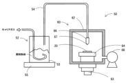
- FIG. 1 is a conceptual diagram showing the configuration of an aerosol deposition (AD) device 50.
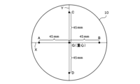
- 1 is a top view of a SiC substrate 10 for explaining a method for measuring the amount of warpage of the SiC substrate 10.
- FIG. 2 is a schematic cross-sectional view of the SiC substrate 10 for explaining a method for measuring the amount of warpage of the SiC substrate 10.
- FIG. 2 is a schematic cross-sectional view of the SiC substrate 10 for explaining a method for measuring the amount of warpage of the SiC substrate 10.
- FIG. 1 is a manufacturing process diagram of a SiC composite substrate 10.
- FIG. 1 is a conceptual diagram showing the configuration of an aerosol deposition (AD) device 50.
- 1 is a top view of a SiC substrate 10 for explaining a method for measuring the amount of warpage of the SiC substrate 10.
- FIG. 2 is a schematic
- SiC substrate The SiC substrate according to the present invention is provided with a biaxially oriented SiC layer.
- the difference between the maximum value k max and the minimum value k min of the Raman shift value is 0.50 cm ⁇ 1 or less in the Si-face and C-face.
- the Raman shift value is a value obtained by measuring Raman shift values showing peaks corresponding to the shear wave acoustic branch of the Raman spectrum at 1 mm intervals on two straight lines passing through the center point of the Si-face and perpendicular to each other in the Si-face of the SiC substrate, and measuring Raman shift values showing peaks corresponding to the shear wave acoustic branch of the Raman spectrum at 1 mm intervals on two straight lines passing through the center point of the C-face and perpendicular to each other in the C-face of the SiC substrate.
- the Si-face and C-face of the SiC substrate are the Si-face and C-face of the biaxially oriented SiC layer when the SiC substrate is composed of a biaxially oriented SiC layer, and are the Si-face and C-face of the composite substrate when the SiC substrate is a composite substrate including a biaxially oriented SiC layer and a SiC single crystal substrate (in this case, the biaxially oriented SiC layer surface may be the Si-face and the SiC single crystal substrate surface may be the C-face, or the biaxially oriented SiC layer surface may be the C-face and the SiC single crystal substrate surface may be the Si-face).
- the Raman shift value showing a peak corresponding to the shear wave acoustic branch of the Raman spectrum typically means a Raman shift value showing a peak of FTA(2/4)E 2 (wave number around 200 cm -1 ). In this way, by controlling the Raman shift value showing a peak corresponding to the shear wave acoustic branch of the Raman spectrum in the SiC substrate, the warpage of the SiC substrate can be reduced.
- controlling the Raman shift value that indicates a peak corresponding to the shear wave acoustic branch of the Raman spectrum in a SiC substrate means that the in-plane distribution of nitrogen and the elastic strain distribution in the SiC substrate can be reduced. It is believed that by reducing the in-plane distribution of nitrogen and the elastic strain distribution in this SiC substrate, warping of the SiC substrate can be reduced.
- the difference between the maximum value k max and the minimum value k min of the obtained Raman shift value is 0.50 cm -1 or less, preferably 0.20 cm -1 or less.
- the Raman shift values showing the peaks corresponding to the shear wave acoustic branch of the Raman spectrum are measured at 1 mm intervals on two straight lines passing through the center point of the Si-face and perpendicular to each other
- the Raman shift values showing the peaks corresponding to the shear wave acoustic branch of the Raman spectrum are measured at 1 mm intervals on two straight lines passing through the center point of the C-face and perpendicular to each other.
- the difference between the maximum value k max and the minimum value k min of the Raman shift value obtained in this way can be regarded as the difference between the maximum value and the minimum value of the Raman shift value when measured over the entire surface (entire region) of the SiC substrate.
- the SiC substrate or biaxially oriented SiC layer has an off-angle, and the off-angle is preferably 0.1 to 12° from the [0001] axis of the SiC substrate or biaxially oriented SiC layer, and more preferably 1 to 5°.
- rare earth elements contained in the biaxially oriented SiC layer include Y, La, Ce, Pr, Nd, Pm, Sm, Eu, Gd, Tb, Dy, Ho, Er, Tm, Yb, Lu, Sc, and combinations thereof. From the viewpoint of reducing warpage of the substrate, the rare earth element is preferably Y or Ce, and more preferably Y.
- the rare earth element concentration of the biaxially oriented SiC layer is preferably 1.0 ⁇ 10 14 to 5.0 ⁇ 10 15 atoms/cm 3 , more preferably 5.0 ⁇ 10 14 to 5.0 ⁇ 10 15 atoms/cm 3 , and even more preferably 5.0 ⁇ 10 14 to 1.4 ⁇ 10 15 atoms/cm 3 .
- the N concentration of the biaxially oriented SiC layer is preferably 1.0 ⁇ 10 18 atoms/cm 3 or more, more preferably 5.0 ⁇ 10 18 atoms/cm 3 or more, and even more preferably 8.0 ⁇ 10 18 atoms/cm 3 or more.
- the upper limit of the N concentration is not particularly limited, but is preferably 1.0 ⁇ 10 21 atoms/cm 3 or less, more preferably 1.0 ⁇ 10 20 atoms/cm 3 or less, and even more preferably 1.0 ⁇ 10 19 atoms/cm 3 or less.
- the biaxially oriented SiC layer is preferably oriented in the c-axis direction and the a-axis direction.
- the SiC substrate is preferably composed of a biaxially oriented SiC layer.
- the biaxially oriented SiC layer may be a SiC single crystal, a SiC polycrystal, or a mosaic crystal, as long as it is oriented in the two axes of the c-axis and the a-axis.
- a mosaic crystal is a collection of crystals that do not have clear grain boundaries but have slightly different orientations in one or both of the c-axis and the a-axis.
- the method for evaluating the orientation is not particularly limited, but known analytical methods such as the EBSD (Electron Back Scatter Diffraction Patterns) method and X-ray pole figures can be used.
- EBSD Electro Back Scatter Diffraction Patterns
- X-ray pole figures can be used.
- the EBSD method inverse pole figure mapping of the surface (plate surface) of the biaxially oriented SiC layer or a cross section perpendicular to the plate surface is measured.
- the SiC layer when the following four conditions are satisfied, (A) the SiC layer is oriented in a specific direction (first axis) approximately normal to the plate surface, (B) the SiC layer is oriented in a specific direction (second axis) approximately in the plate surface direction perpendicular to the first axis, (C) the inclination angle from the first axis is distributed within ⁇ 10°, and (D) the inclination angle from the second axis is distributed within ⁇ 10°, the SiC layer can be defined as being oriented in two axes, the approximately normal direction and the approximately plate surface direction.
- the SiC layer is determined to be oriented in two axes, the c-axis and the a-axis.
- the approximately normal direction of the plate surface is oriented to the c-axis
- the approximately in-plane direction may be oriented in a specific direction (e.g., the a-axis) perpendicular to the c-axis.
- the biaxially oriented SiC layer may be oriented in two axes, the approximately normal direction and the approximately in-plane direction, but it is preferable that the approximately normal direction is oriented to the c-axis.
- the tilt angle distribution in the approximately normal direction and/or the approximately in-plane direction the smaller the mosaic property of the biaxially oriented SiC layer, and the closer it is to zero, the closer it is to a single crystal. Therefore, from the viewpoint of the crystallinity of the biaxially oriented SiC layer, it is preferable that the tilt angle distribution is small in both the approximately normal direction and the approximately in-plane direction, for example, ⁇ 5° or less is more preferable, and ⁇ 3° or less is even more preferable.
- the SiC substrate of the present invention is preferably in the form of a SiC composite substrate. That is, according to a preferred embodiment of the present invention, a SiC composite substrate is provided that includes a SiC single crystal substrate and the above-mentioned SiC substrate on the SiC single crystal substrate. In this way, the SiC composite substrate includes a SiC substrate with a controlled Raman shift value that shows a peak corresponding to the shear wave acoustic branch of the Raman spectrum, thereby making it possible to reduce warpage of the SiC composite substrate.
- a SiC single crystal substrate is typically a layer composed of a SiC single crystal, and has a crystal growth surface.
- the polytype and off-angle of the SiC single crystal are not particularly limited, but the polytype is preferably 4H or 6H, and the off-angle is preferably 0.1 to 12° from the [0001] axis of the single crystal SiC. It is more preferable that the polytype is 4H, and the off-angle is 1 to 5° from the [0001] axis of the single crystal SiC.
- the SiC substrate of the present invention may be in the form of a free-standing substrate of a biaxially oriented SiC layer alone, or in the form of a SiC composite substrate accompanied by a SiC single crystal substrate. Therefore, if necessary, the biaxially oriented SiC layer may be finally separated from the SiC single crystal substrate.
- the separation of the SiC single crystal substrate may be performed by a known method, and is not particularly limited. For example, a method of separating the biaxially oriented SiC layer using a wire saw, a method of separating the biaxially oriented SiC layer using electric discharge machining, a method of separating the biaxially oriented SiC layer using a laser, etc. may be mentioned.
- the biaxially oriented SiC layer may be placed on another support substrate.
- the material of the other support substrate is not particularly limited, but a suitable one may be selected from the viewpoint of material properties.
- a metal substrate such as Cu, a ceramic substrate such as SiC or AlN, etc. may be mentioned.
- the SiC composite substrate having the SiC substrate of the present invention can be preferably manufactured by (a) forming a predetermined oriented precursor layer on a SiC single crystal substrate, (b) heat-treating the oriented precursor layer on the SiC single crystal substrate to convert at least the portion near the SiC single crystal substrate into a SiC substrate (biaxially oriented SiC layer), and optionally (c) performing processing such as grinding or polishing to expose the surface of the biaxially oriented SiC layer.
- processing such as grinding or polishing to expose the surface of the biaxially oriented SiC layer.
- there is no limitation on the manufacturing method of the SiC composite substrate as long as it is possible to obtain a SiC substrate with a controlled Raman shift value that shows a peak corresponding to the shear wave acoustic branch of the Raman spectrum.
- the manufacturing method is capable of increasing the flow rate of nitrogen during heat treatment, and in that case, it may be a gas phase method such as CVD or sublimation method, or a liquid phase method such as a solution method.
- the rare earth element concentration and/or N concentration in the SiC substrate (biaxially oriented SiC layer) can be preferably controlled by adding a rare earth compound to the raw material when forming the oriented precursor layer, or by changing the heat treatment conditions (gas flow rate, heat treatment temperature, holding time, etc.).
- Figure 1 is a longitudinal cross-sectional view of a SiC composite substrate 10 (a cross-sectional view of the SiC composite substrate 10 cut longitudinally along a plane including the central axis of the SiC composite substrate 10), and Figure 2 is a manufacturing process diagram for the SiC composite substrate 10.
- the SiC composite substrate 10 of this embodiment includes a SiC single crystal substrate 20 and a SiC substrate 30 on the SiC single crystal substrate.
- the textured precursor layer 40 becomes the SiC substrate (biaxially textured SiC layer) 30 by heat treatment, which will be described later.
- the textured precursor layer 40 is formed on the crystal growth surface of the SiC single crystal substrate 20.
- the method of forming the oriented precursor layer 40 can be a known method.
- the method of forming the oriented precursor layer 40 can be, for example, a solid-phase film formation method such as an AD (aerosol deposition) method or an HPPD (supersonic plasma particle deposition) method, a gas-phase film formation method such as a sputtering method, a vapor deposition method, a sublimation method, or various CVD (chemical vapor deposition) methods, or a liquid-phase film formation method such as a solution growth method.
- a method of forming the oriented precursor layer 40 directly on the SiC single crystal substrate 20 can be used.
- a thermal CVD method for example, a thermal CVD method, a plasma CVD method, a mist CVD method, an MO (metal organic) CVD method, or the like can be used.
- a method of using a polycrystalline body prepared in advance by a sublimation method, various CVD methods, sintering, or the like as the oriented precursor layer 40 and placing it on the SiC single crystal substrate 20 can also be used.
- a method of preparing a molded body of the oriented precursor layer 40 in advance and placing this molded body on the SiC single crystal substrate 20 may be used.
- Such an orientation precursor layer 40 may be a tape molded body produced by tape casting, or a green compact produced by pressure molding such as a uniaxial press.
- the raw materials for the oriented precursor layers 40 contain a rare earth compound.
- the rare earth compound is not particularly limited, but examples include oxides, nitrides, carbides, and fluorides of at least one of the 17 rare earth elements mentioned above. Oxides of rare earth elements are preferable as the rare earth compound.
- the oriented precursor layer 40 In the method of forming the oriented precursor layer 40 directly on the SiC single crystal substrate 20, when various CVD methods, sublimation methods, solution growth methods, etc. are used, epitaxial growth may occur on the SiC single crystal substrate 20 without going through the heat treatment process described below, and the SiC substrate 30 may be formed.
- the oriented precursor layer 40 is in an unoriented state when formed, that is, it is an amorphous or unoriented polycrystal, and it is preferable to orient it using the SiC single crystal as a seed in the subsequent heat treatment process. In this way, it is possible to effectively reduce crystal defects that reach the surface of the SiC substrate 30.
- the re-arrangement of the crystal structure of the solid-phase oriented precursor layer once formed using the SiC single crystal as a seed may also be effective in eliminating crystal defects. Therefore, when various CVD methods, sublimation methods, solution growth methods, etc. are used, it is preferable to select conditions that do not cause epitaxial growth in the formation process of the oriented precursor layer 40.
- the method of forming the oriented precursor layer 40 directly on the SiC single crystal substrate 20 by the AD method or various CVD methods, or the method of placing a polycrystalline body separately prepared by sublimation, various CVD methods, sintering, etc. on the SiC single crystal substrate 20 is preferable.
- the AD method is particularly preferable because it does not require a high vacuum process and the film formation speed is relatively fast.
- the method of directly forming the oriented precursor layer 40 is preferable.
- the method of placing a pre-prepared molded body on the SiC single crystal substrate 20 is also preferable as a simple method, but since the oriented precursor layer 40 is made of powder, a sintering process is required in the heat treatment step described later. Both methods can use known conditions, but below we will describe a method of forming an orientation precursor layer 40 directly on a SiC single crystal substrate 20 by AD or thermal CVD, and a method of placing a previously prepared molded body on a SiC single crystal substrate 20.
- the AD method is a technology in which fine particles or fine particle raw material are mixed with a gas to form an aerosol, and this aerosol is sprayed at high speed from a nozzle to collide with a substrate to form a coating, and has the characteristic that the coating can be formed at room temperature.
- An example of a film formation apparatus (AD apparatus) used in such an AD method is shown in Figure 3.
- the AD apparatus 50 shown in Figure 3 is configured as an apparatus used in the AD method in which raw material powder is sprayed onto a substrate under an atmosphere with a lower pressure than atmospheric pressure.
- This AD apparatus 50 includes an aerosol generation section 52 that generates an aerosol of raw material powder containing raw material components, and a film formation section 60 that sprays the raw material powder onto a SiC single crystal substrate 20 to form a film containing the raw material components.
- the aerosol generating section 52 includes an aerosol generating chamber 53 that contains raw material powder and generates aerosol by receiving a carrier gas from a gas cylinder (not shown), a raw material supply pipe 54 that supplies the generated aerosol to the film forming section 60, and a vibrator 55 that applies vibrations at a frequency of 10 to 100 Hz to the aerosol generating chamber 53 and the aerosol therein.
- the film forming section 60 includes a film forming chamber 62 that sprays the aerosol onto the SiC single crystal substrate 20, a substrate holder 64 that is disposed inside the film forming chamber 62 and fixes the SiC single crystal substrate 20, and an XY stage 63 that moves the substrate holder 64 in the X-axis and Y-axis directions.
- the film forming section 60 also includes an injection nozzle 66 that has a slit 67 formed at its tip and sprays the aerosol onto the SiC single crystal substrate 20, and a vacuum pump 68 that reduces the pressure in the film forming chamber 62.
- the injection nozzle 66 is attached to the tip of the raw material supply pipe 54.
- the AD method can cause pores in the film or the film to become a compact, depending on the deposition conditions. For example, it is easily affected by the collision speed of the raw material powder with the substrate, the particle size of the raw material powder, the agglomeration state of the raw material powder in the aerosol, the amount sprayed per unit time, etc.
- the collision speed of the raw material powder with the substrate is affected by the pressure difference between the deposition chamber 62 and the spray nozzle 66, the opening area of the spray nozzle, etc. For this reason, in order to obtain a dense oriented precursor layer, it is necessary to appropriately control these factors.
- the source gas is not particularly limited, but silicon tetrachloride (SiCl 4 ) gas or silane (SiH 4 ) gas can be used as a Si source, and methane (CH 4 ) gas or propane (C 3 H 8 ) gas can be used as a C source.
- the deposition temperature is preferably 1000 to 2200°C, more preferably 1100 to 2000°C, and even more preferably 1200 to 1900°C.
- the oriented precursor layer 40 is not oriented when it is produced, that is, it is amorphous or unoriented polycrystalline, and it is preferable to use a SiC single crystal as a seed crystal during the heat treatment process to cause crystal rearrangement. It is known that the film formation temperature, the gas flow rate of the Si source and the C source and their ratio, the film formation pressure, etc. have an effect on the formation of an amorphous or polycrystalline layer on a SiC single crystal using a thermal CVD method.
- the film formation temperature has a large effect, and from the viewpoint of forming an amorphous or polycrystalline layer, a low film formation temperature is preferable, preferably less than 1700°C, more preferably 1500°C or less, and even more preferably 1400°C or less. However, if the film formation temperature is too low, the film formation rate itself also decreases, so from the viewpoint of the film formation rate, a high film formation temperature is preferable.
- the orientation precursor layer 40 can be prepared by molding the raw material powder of the orientation precursor.
- the orientation precursor layer 40 is a press molded body.
- the press molded body can be prepared by press molding the raw material powder of the orientation precursor based on a known method, for example, by putting the raw material powder into a mold and pressing it at a pressure of preferably 100 to 400 kgf/cm 2 , more preferably 150 to 300 kgf/cm 2.
- there is no particular limitation on the molding method and in addition to press molding, tape molding, extrusion molding, casting molding, doctor blade method, and any combination thereof can be used.
- additives such as binders, plasticizers, dispersants, and dispersion media are appropriately added to the raw material powder to make a slurry, and the slurry is preferably discharged and molded into a sheet by passing it through a thin slit-shaped discharge port.
- the thickness of the molded body molded into a sheet there is no limitation on the thickness of the molded body molded into a sheet, but from the viewpoint of handling, it is preferable that it is 5 to 500 ⁇ m.
- a number of these sheet molded bodies may be stacked and used to obtain the desired thickness. These molded bodies are then heat-treated on the SiC single crystal substrate 20, and the portions near the SiC single crystal substrate 20 become the SiC substrate 30.
- the molded body it is necessary to sinter the molded body in the heat treatment process described below. It is preferable to form the SiC substrate 30 after the molded body is sintered and integrated with the SiC single crystal substrate 20 as a polycrystalline body. If the molded body does not go through the sintered state, epitaxial growth using the SiC single crystal as a seed may not occur sufficiently. For this reason, the molded body may contain additives such as sintering aids in addition to the SiC raw material.
- the SiC substrate 30 is generated by heat treating the laminate in which the orientation precursor layer 40 is laminated or placed on the SiC single crystal substrate 20.
- the heat treatment method is not particularly limited as long as epitaxial growth occurs using the SiC single crystal substrate 20 as a seed, and can be performed in a known heat treatment furnace such as a tubular furnace or a hot plate. In addition to these normal pressure (pressless) heat treatments, pressurized heat treatments such as hot pressing and HIP, and combinations of normal pressure heat treatment and pressurized heat treatment can also be used.
- the heat treatment atmosphere is preferably an inert gas atmosphere containing nitrogen.
- the nitrogen-containing inert gas is preferably a mixed gas containing nitrogen and argon, and the flow rate of nitrogen at that time is, for example, 0.5 to 15 L/min, and the flow rate of argon is, for example, 3 to 100 L/min.
- the heat treatment temperature is preferably 1700 to 2700° C. By increasing the temperature, the orientation precursor layer 40 is likely to grow while being oriented to the c-axis and a-axis with the SiC single crystal substrate 20 as a seed crystal. Therefore, the heat treatment temperature is preferably 1700°C or higher, more preferably 1800°C or higher, even more preferably 1900°C or higher, and particularly preferably 2200°C or higher.
- the heat treatment temperature is preferably 2700°C or lower, more preferably 2500°C or lower.
- the heat treatment conditions affect the content of rare earth elements in the biaxially oriented SiC layer, it is preferable to appropriately control the conditions (for example, heat treatment temperature and holding time).
- the heat treatment temperature is preferably 1900 to 2700°C, more preferably 2200 to 2600°C, and even more preferably 2400 to 2500°C.
- the holding time is preferably 2 to 30 hours, more preferably 4 to 20 hours.
- the heat treatment temperature and holding time are related to the thickness of the SiC substrate 30 produced by epitaxial growth, and can be adjusted as appropriate.
- the orientation precursor layer 40 when a molded body prepared in advance is used as the orientation precursor layer 40, it is necessary to sinter it during the heat treatment, and high-temperature atmospheric sintering, hot pressing, HIP, or a combination thereof is suitable.
- the surface pressure is preferably 50 kgf/cm 2 or more, more preferably 100 kgf/cm 2 or more, and even more preferably 200 kgf/cm 2 or more, and there is no particular upper limit.
- the sintering temperature is also not particularly limited as long as sintering and epitaxial growth occur.
- the sintering conditions affect the content of rare earth elements in the biaxially oriented SiC layer, it is preferable to appropriately control the conditions (for example, the sintering temperature and holding time).
- the sintering temperature is preferably 1700 to 2700 ° C.
- the holding time is preferably 2 to 18 hours.
- the atmosphere during sintering can be selected from vacuum, nitrogen, inert gas, or a mixed gas of nitrogen and inert gas.
- sintering may be performed in multiple stages, and the sintering temperature and total holding time are preferably within the above range.
- the SiC powder used as the raw material may be composed of at least one of ⁇ -SiC and ⁇ -SiC, but is preferably composed of ⁇ -SiC.
- the SiC powder is preferably composed of SiC particles having an average particle size of 0.01 to 100 ⁇ m.
- the average particle size refers to the average value obtained by observing the powder with a scanning electron microscope and measuring the maximum diameter in a certain direction for 100 primary particles.
- the crystals in the oriented precursor layer 40 grow from the crystal growth surface of the SiC single crystal substrate 20 while being oriented in the c-axis and a-axis, so that the oriented precursor layer 40 gradually changes from the crystal growth surface into the SiC substrate 30.
- the SiC composite substrate including the resulting SiC substrate 30 has a controlled Raman shift value, which indicates a peak corresponding to the shear wave acoustic branch of the Raman spectrum, and has reduced warping. The exact mechanism behind this is unclear, but it is thought that, for example, by increasing the flow rate of nitrogen during heat treatment, the uniformity of the nitrogen concentration and heat distribution increases, resulting in reduced warping.
- the orientation precursor layer 40 remaining on the SiC substrate 30 after the heat treatment step is ground and removed to expose the surface of the SiC substrate 30, and the exposed surface is ground and/or polished. In this manner, the SiC composite substrate 10 is obtained.
- the present invention is not limited to the above-described embodiment, and may be embodied in various forms within the technical scope of the present invention.
- only one layer of SiC substrate 30 is provided on SiC single crystal substrate 20, but two or more layers may be provided.
- a second layer of SiC substrate 30 can be provided on SiC substrate 30 by stacking an orientation precursor layer 40 on SiC substrate 30 of SiC composite substrate 10, heat treating the substrate, and then grinding and/or polishing the substrate in this order.
- Example 1 (1) Preparation of Oriented Precursor Layer A raw material powder containing 93.0% by weight of commercially available fine ⁇ -SiC powder (volume-based D50 particle size: 0.7 ⁇ m) and 7.0% by weight of yttrium oxide powder (volume-based D50 particle size: 0.1 ⁇ m) was prepared. The raw material powder was mixed in ethanol for 24 hours using SiC balls in a ball mill, and then dried to obtain a mixed powder.
- a commercially available SiC single crystal substrate (n-type 4H-SiC, diameter 100 mm (4 inches), Si face, (0001) face, off angle 4°, thickness 0.35 mm, no orientation flat) was prepared as a SiC single crystal layer, and the mixed powder was sprayed onto the SiC single crystal substrate in the AD device 50 shown in FIG. 3 to form an AD film (oriented precursor layer).
- the AD deposition conditions were as follows. First, the carrier gas was He, and the deposition was performed using a ceramic nozzle with a slit of 5 mm long side x 0.4 mm short side. The nozzle was scanned at a scanning speed of 0.5 mm/s, with the nozzle moving 105 mm in the forward direction perpendicular to the long side of the slit, 5 mm in the long side direction of the slit, 105 mm in the return direction perpendicular to the long side of the slit, and 5 mm in the long side direction of the slit opposite the initial position. When the nozzle had moved 105 mm from the initial position in the long side direction of the slit, it scanned in the opposite direction and returned to the initial position. This cycle was repeated 4000 times. The thickness of the AD film formed in this way was approximately 400 ⁇ m.
- the Raman shift values showing peaks corresponding to the shear wave acoustic branch of the Raman spectrum were measured at 1 mm intervals on two straight lines passing through the center point of the (0001) plane (i.e., Si plane) of the obtained SiC substrate and perpendicular to each other.
- the Raman shift values showing peaks corresponding to the shear wave acoustic branch of the Raman spectrum were measured at 1 mm intervals on two straight lines passing through the center point of the (000-1) plane (i.e., C plane) of the obtained SiC substrate and perpendicular to each other.
- the measurement conditions at this time are shown below.
- the Raman shift value showing a peak corresponding to the shear wave acoustic branch of the Raman spectrum means the Raman shift value showing a peak of FTA(2/4)E 2 (near a wave number of 200 cm -1 ).
- Light source Semiconductor pumped solid-state laser (DPSS, 532 nm, 100 mW) ⁇ Diffraction grating: 1800 gr/mm
- Optical system backscattering configuration
- Objective lens 100x Laser irradiation time: 5 seconds
- a point P on the curve AB was determined so that the distance of the line segment was the longest (for example, in FIG. 5, there are points P and O as arbitrary points on the curve AB, and among the line segments extending perpendicularly from each point to the line segment AB, the line segment extending from point P is the longest).
- the distance between the line segment AB and point P was determined as the warpage amount ⁇ . Also, as shown in FIG.
- a point R on the curve CD was determined so that the distance of the line segment was the longest (for example, in FIG. 6, there are points R and O as arbitrary points on the curve CD, and among the line segments extending perpendicularly from each point to the line segment CD, the line segment extending from point R is the longest).
- the distance between the line segment CD and the point R was taken as the amount of warpage ⁇ .
- the average value of these amounts of warpage ⁇ and ⁇ was taken as the amount of warpage of the SiC substrate.
- Table 1 The amount of warpage can be measured by the above-mentioned measurement method whether the SiC substrate 10 is warped in a convex shape or in a concave shape.
- Example 2 In the above (2), except that the flow rate of argon was 45 L/min and the flow rate of nitrogen was 5 L/min, the same procedure as in Example 1 was followed to produce and evaluate a SiC substrate. The heat-treated layer obtained was confirmed to be a biaxially oriented SiC layer. The results are shown in Table 1.
- Example 3 In the above (2), except that the flow rate of argon was 90 L/min and the flow rate of nitrogen was 10 L/min, the same procedure as in Example 1 was followed to produce and evaluate a SiC substrate. The heat-treated layer obtained was confirmed to be a biaxially oriented SiC layer. The results are shown in Table 1.
- Example 4 In the above (2), except that the flow rate of argon was 5 L/min and the flow rate of nitrogen was 0.5 L/min, the same procedure as in Example 1 was followed to produce and evaluate a SiC substrate. The heat-treated layer obtained was confirmed to be a biaxially oriented SiC layer. The results are shown in Table 1.
- Example 5 In the above (1), a SiC substrate was produced and evaluated in the same manner as in Example 1, except that a raw material powder containing 91.7% by weight of commercially available fine ⁇ -SiC powder (volume-based D50 particle size: 0.7 ⁇ m) and 8.3% by weight of yttrium oxide powder (volume-based D50 particle size: 0.1 ⁇ m) was used. The obtained heat-treated layer was confirmed to be a biaxially oriented SiC layer. The results are shown in Table 1.
- Example 6 In the above (1), a SiC substrate was produced and evaluated in the same manner as in Example 1, except that a raw material powder containing 95.2% by weight of commercially available fine ⁇ -SiC powder (volume-based D50 particle size: 0.7 ⁇ m) and 4.8% by weight of yttrium oxide powder (volume-based D50 particle size: 0.1 ⁇ m) was used. The obtained heat-treated layer was confirmed to be a biaxially oriented SiC layer. The results are shown in Table 1.
- Example 7 In the above (1), a SiC substrate was produced and evaluated in the same manner as in Example 1, except that a raw material powder containing 93.0% by weight of commercially available fine ⁇ -SiC powder (volume-based D50 particle size: 0.7 ⁇ m) and 7.0% by weight of yttrium oxide powder (volume-based D50 particle size: 0.1 ⁇ m) was used. The obtained heat-treated layer was confirmed to be a biaxially oriented SiC layer. The results are shown in Table 1.
- Example 8 (Comparative) In the above (2), except that the flow rate of argon was 2.7 L/min and the flow rate of nitrogen was 0.3 L/min, the same procedure as in Example 1 was followed to produce and evaluate a SiC substrate. The obtained heat-treated layer was confirmed to be a biaxially oriented SiC layer. The results are shown in Table 1.
- Example 9 (Comparison) In the above (2), except that the flow rate of argon was 0.9 L/min and the flow rate of nitrogen was 0.1 L/min, the same procedure as in Example 1 was followed to produce and evaluate a SiC substrate. The obtained heat-treated layer was confirmed to be a biaxially oriented SiC layer. The results are shown in Table 1.
Landscapes
- Chemical & Material Sciences (AREA)
- Metallurgy (AREA)
- Engineering & Computer Science (AREA)
- Crystallography & Structural Chemistry (AREA)
- Materials Engineering (AREA)
- Organic Chemistry (AREA)
- Inorganic Chemistry (AREA)
- Thermal Sciences (AREA)
- Physics & Mathematics (AREA)
- Crystals, And After-Treatments Of Crystals (AREA)
- Investigating, Analyzing Materials By Fluorescence Or Luminescence (AREA)
- Laminated Bodies (AREA)
- Carbon And Carbon Compounds (AREA)
Priority Applications (4)
| Application Number | Priority Date | Filing Date | Title |
|---|---|---|---|
| JP2025516502A JPWO2024224665A1 (https=) | 2023-04-27 | 2023-11-14 | |
| CN202380096444.7A CN121002235A (zh) | 2023-04-27 | 2023-11-14 | SiC基板及SiC复合基板 |
| EP23935437.6A EP4703502A1 (en) | 2023-04-27 | 2023-11-14 | Sic substrate and sic composite substrate |
| US19/361,101 US20260043171A1 (en) | 2023-04-27 | 2025-10-17 | SiC SUBSTRATE AND SiC COMPOSITE SUBSTRATE |
Applications Claiming Priority (2)
| Application Number | Priority Date | Filing Date | Title |
|---|---|---|---|
| JP2023-073297 | 2023-04-27 | ||
| JP2023073297 | 2023-04-27 |
Related Child Applications (1)
| Application Number | Title | Priority Date | Filing Date |
|---|---|---|---|
| US19/361,101 Continuation US20260043171A1 (en) | 2023-04-27 | 2025-10-17 | SiC SUBSTRATE AND SiC COMPOSITE SUBSTRATE |
Publications (1)
| Publication Number | Publication Date |
|---|---|
| WO2024224665A1 true WO2024224665A1 (ja) | 2024-10-31 |
Family
ID=93255813
Family Applications (1)
| Application Number | Title | Priority Date | Filing Date |
|---|---|---|---|
| PCT/JP2023/040963 Ceased WO2024224665A1 (ja) | 2023-04-27 | 2023-11-14 | SiC基板及びSiC複合基板 |
Country Status (5)
| Country | Link |
|---|---|
| US (1) | US20260043171A1 (https=) |
| EP (1) | EP4703502A1 (https=) |
| JP (1) | JPWO2024224665A1 (https=) |
| CN (1) | CN121002235A (https=) |
| WO (1) | WO2024224665A1 (https=) |
Citations (8)
| Publication number | Priority date | Publication date | Assignee | Title |
|---|---|---|---|---|
| JP2015059073A (ja) * | 2013-09-20 | 2015-03-30 | 新日鉄住金マテリアルズ株式会社 | 炭化珪素単結晶ウェハの内部応力評価方法、及び炭化珪素単結晶ウェハの反りの予測方法 |
| WO2016067918A1 (ja) * | 2014-10-31 | 2016-05-06 | 富士電機株式会社 | 炭化珪素エピタキシャル膜の成長方法 |
| JP2016164120A (ja) | 2016-03-15 | 2016-09-08 | 新日鉄住金マテリアルズ株式会社 | 炭化珪素単結晶ウェハ |
| WO2017057742A1 (ja) | 2015-10-02 | 2017-04-06 | 新日鐵住金株式会社 | SiC単結晶インゴット |
| JP2017075074A (ja) | 2015-10-15 | 2017-04-20 | 住友電気工業株式会社 | 炭化珪素基板 |
| WO2021111835A1 (ja) | 2019-12-02 | 2021-06-10 | 住友電気工業株式会社 | 炭化珪素基板および炭化珪素基板の製造方法 |
| JP2022120059A (ja) | 2017-12-08 | 2022-08-17 | 住友電気工業株式会社 | 炭化珪素基板および炭化珪素エピタキシャル基板 |
| WO2022191751A1 (en) * | 2021-03-11 | 2022-09-15 | Kiselkarbid I Stockholm Ab | System and method of producing monocrystalline layers on a substrate |
Family Cites Families (4)
| Publication number | Priority date | Publication date | Assignee | Title |
|---|---|---|---|---|
| JP6515757B2 (ja) * | 2015-09-15 | 2019-05-22 | 信越化学工業株式会社 | SiC複合基板の製造方法 |
| JP7212139B2 (ja) * | 2019-03-11 | 2023-01-24 | 日本碍子株式会社 | SiC複合基板及び半導体デバイス |
| WO2021149598A1 (ja) * | 2020-01-24 | 2021-07-29 | 日本碍子株式会社 | 二軸配向SiC複合基板及び半導体デバイス用複合基板 |
| WO2023062850A1 (ja) * | 2021-10-12 | 2023-04-20 | 日本碍子株式会社 | 希土類含有SiC基板及びSiC複合基板 |
-
2023
- 2023-11-14 JP JP2025516502A patent/JPWO2024224665A1/ja active Pending
- 2023-11-14 WO PCT/JP2023/040963 patent/WO2024224665A1/ja not_active Ceased
- 2023-11-14 CN CN202380096444.7A patent/CN121002235A/zh active Pending
- 2023-11-14 EP EP23935437.6A patent/EP4703502A1/en active Pending
-
2025
- 2025-10-17 US US19/361,101 patent/US20260043171A1/en active Pending
Patent Citations (8)
| Publication number | Priority date | Publication date | Assignee | Title |
|---|---|---|---|---|
| JP2015059073A (ja) * | 2013-09-20 | 2015-03-30 | 新日鉄住金マテリアルズ株式会社 | 炭化珪素単結晶ウェハの内部応力評価方法、及び炭化珪素単結晶ウェハの反りの予測方法 |
| WO2016067918A1 (ja) * | 2014-10-31 | 2016-05-06 | 富士電機株式会社 | 炭化珪素エピタキシャル膜の成長方法 |
| WO2017057742A1 (ja) | 2015-10-02 | 2017-04-06 | 新日鐵住金株式会社 | SiC単結晶インゴット |
| JP2017075074A (ja) | 2015-10-15 | 2017-04-20 | 住友電気工業株式会社 | 炭化珪素基板 |
| JP2016164120A (ja) | 2016-03-15 | 2016-09-08 | 新日鉄住金マテリアルズ株式会社 | 炭化珪素単結晶ウェハ |
| JP2022120059A (ja) | 2017-12-08 | 2022-08-17 | 住友電気工業株式会社 | 炭化珪素基板および炭化珪素エピタキシャル基板 |
| WO2021111835A1 (ja) | 2019-12-02 | 2021-06-10 | 住友電気工業株式会社 | 炭化珪素基板および炭化珪素基板の製造方法 |
| WO2022191751A1 (en) * | 2021-03-11 | 2022-09-15 | Kiselkarbid I Stockholm Ab | System and method of producing monocrystalline layers on a substrate |
Non-Patent Citations (3)
| Title |
|---|
| NAKASHIMA, SHINICHI ET AL.: "23p-ZQ-12 Measurement of surface phonons and determination of polar surface of SiC by DUV Raman scattering spectroscopy. entire text", LECTURE PREPRINTS OF THE 53RD SPRING MEETING OF THE JAPAN SOCIETY OF APPLIED PHYSICS AND RELATED SOCIETIES JSAP; TOKYO, JAPAN; MAR 22-26, 2006, vol. 53, 1 January 2006 (2006-01-01) - 26 March 2006 (2006-03-26), pages 419, XP009559292 * |
| See also references of EP4703502A1 |
| TAKENAKA KAZUMASA, BANDO YOTA, TAKIDANI YUSUKE, YAMAGUCHI MAKOTO, TANAKA YASUHIRO, NAKASHIMA SHIN-ICHI, OKADA TATSUTA, TOMITA TA: " The surface polarity dependences of the Raman spectrum in sub-micrometer thick 4H-SiC substrate", LECTURE PREPRINTS OF THE 65TH JSAP SPRING MEETING (2018), 1 January 2018 (2018-01-01), XP093230110 * |
Also Published As
| Publication number | Publication date |
|---|---|
| CN121002235A (zh) | 2025-11-21 |
| US20260043171A1 (en) | 2026-02-12 |
| EP4703502A1 (en) | 2026-03-04 |
| JPWO2024224665A1 (https=) | 2024-10-31 |
Similar Documents
| Publication | Publication Date | Title |
|---|---|---|
| JP7628968B2 (ja) | 二軸配向SiC複合基板及び半導体デバイス用複合基板 | |
| JP7282214B2 (ja) | 希土類含有SiC基板及びSiCエピタキシャル層の製法 | |
| CN113574215A (zh) | 基底基板及其制造方法 | |
| JP7538900B2 (ja) | 希土類含有SiC基板及びそれを用いたSiC複合基板 | |
| US12080551B2 (en) | SiC composite substrate including biaxially oreinted SiC layer and semiconductor device | |
| US20210384300A1 (en) | SiC COMPOSITE SUBSTRATE AND COMPOSITE SUBSTRATE FOR SEMICONDUCTOR DEVICE | |
| WO2023062850A1 (ja) | 希土類含有SiC基板及びSiC複合基板 | |
| JP7636908B2 (ja) | SiC複合基板 | |
| JP7372312B2 (ja) | SiC複合基板及び半導体デバイス用複合基板 | |
| JP7265624B2 (ja) | 半導体膜 | |
| JP7587688B2 (ja) | SiC基板及びSiC複合基板 | |
| WO2024224665A1 (ja) | SiC基板及びSiC複合基板 | |
| JP7686016B2 (ja) | SiC基板及びSiC複合基板 | |
| JP7104266B1 (ja) | 希土類含有SiC基板及びSiC複合基板 | |
| WO2024202200A1 (ja) | SiC基板及びSiC複合基板 | |
| US20250391657A1 (en) | Base substrate | |
| WO2025083939A1 (ja) | SiC基板及びSiC複合基板 | |
| WO2025203572A1 (ja) | 下地基板 |
Legal Events
| Date | Code | Title | Description |
|---|---|---|---|
| 121 | Ep: the epo has been informed by wipo that ep was designated in this application |
Ref document number: 23935437 Country of ref document: EP Kind code of ref document: A1 |
|
| ENP | Entry into the national phase |
Ref document number: 2025516502 Country of ref document: JP Kind code of ref document: A |
|
| WWE | Wipo information: entry into national phase |
Ref document number: 2025516502 Country of ref document: JP |
|
| WWE | Wipo information: entry into national phase |
Ref document number: 2023935437 Country of ref document: EP |
|
| NENP | Non-entry into the national phase |
Ref country code: DE |
|
| ENP | Entry into the national phase |
Ref document number: 2023935437 Country of ref document: EP Effective date: 20251127 |
|
| ENP | Entry into the national phase |
Ref document number: 2023935437 Country of ref document: EP Effective date: 20251127 |
|
| ENP | Entry into the national phase |
Ref document number: 2023935437 Country of ref document: EP Effective date: 20251127 |
|
| ENP | Entry into the national phase |
Ref document number: 2023935437 Country of ref document: EP Effective date: 20251127 |
|
| ENP | Entry into the national phase |
Ref document number: 2023935437 Country of ref document: EP Effective date: 20251127 |
|
| ENP | Entry into the national phase |
Ref document number: 2023935437 Country of ref document: EP Effective date: 20251127 |
|
| ENP | Entry into the national phase |
Ref document number: 2023935437 Country of ref document: EP Effective date: 20251127 |
|
| ENP | Entry into the national phase |
Ref document number: 2023935437 Country of ref document: EP Effective date: 20251127 |
|
| ENP | Entry into the national phase |
Ref document number: 2023935437 Country of ref document: EP Effective date: 20251127 |
|
| WWP | Wipo information: published in national office |
Ref document number: 2023935437 Country of ref document: EP |