WO2024218897A1 - プリント配線基板用露光装置、露光方法及びプリント配線基板の製造方法 - Google Patents
プリント配線基板用露光装置、露光方法及びプリント配線基板の製造方法 Download PDFInfo
- Publication number
- WO2024218897A1 WO2024218897A1 PCT/JP2023/015608 JP2023015608W WO2024218897A1 WO 2024218897 A1 WO2024218897 A1 WO 2024218897A1 JP 2023015608 W JP2023015608 W JP 2023015608W WO 2024218897 A1 WO2024218897 A1 WO 2024218897A1
- Authority
- WO
- WIPO (PCT)
- Prior art keywords
- substrate
- mask
- exposure
- laser beam
- irradiation
- Prior art date
- Legal status (The legal status is an assumption and is not a legal conclusion. Google has not performed a legal analysis and makes no representation as to the accuracy of the status listed.)
- Ceased
Links
Images


Classifications
-
- G—PHYSICS
- G03—PHOTOGRAPHY; CINEMATOGRAPHY; ANALOGOUS TECHNIQUES USING WAVES OTHER THAN OPTICAL WAVES; ELECTROGRAPHY; HOLOGRAPHY
- G03F—PHOTOMECHANICAL PRODUCTION OF TEXTURED OR PATTERNED SURFACES, e.g. FOR PRINTING, FOR PROCESSING OF SEMICONDUCTOR DEVICES; MATERIALS THEREFOR; ORIGINALS THEREFOR; APPARATUS SPECIALLY ADAPTED THEREFOR
- G03F7/00—Photomechanical, e.g. photolithographic, production of textured or patterned surfaces, e.g. printing surfaces; Materials therefor, e.g. comprising photoresists; Apparatus specially adapted therefor
- G03F7/20—Exposure; Apparatus therefor
- G03F7/2002—Exposure; Apparatus therefor with visible light or UV light, through an original having an opaque pattern on a transparent support, e.g. film printing, projection printing; by reflection of visible or UV light from an original such as a printed image
- G03F7/201—Exposure; Apparatus therefor with visible light or UV light, through an original having an opaque pattern on a transparent support, e.g. film printing, projection printing; by reflection of visible or UV light from an original such as a printed image characterised by an oblique exposure; characterised by the use of plural sources; characterised by the rotation of the optical device; characterised by a relative movement of the optical device, the light source, the sensitive system or the mask
-
- G—PHYSICS
- G03—PHOTOGRAPHY; CINEMATOGRAPHY; ANALOGOUS TECHNIQUES USING WAVES OTHER THAN OPTICAL WAVES; ELECTROGRAPHY; HOLOGRAPHY
- G03F—PHOTOMECHANICAL PRODUCTION OF TEXTURED OR PATTERNED SURFACES, e.g. FOR PRINTING, FOR PROCESSING OF SEMICONDUCTOR DEVICES; MATERIALS THEREFOR; ORIGINALS THEREFOR; APPARATUS SPECIALLY ADAPTED THEREFOR
- G03F7/00—Photomechanical, e.g. photolithographic, production of textured or patterned surfaces, e.g. printing surfaces; Materials therefor, e.g. comprising photoresists; Apparatus specially adapted therefor
- G03F7/70—Microphotolithographic exposure; Apparatus therefor
- G03F7/70383—Direct write, i.e. pattern is written directly without the use of a mask by one or multiple beams
Definitions
- the present invention relates to an exposure device for printed wiring boards, an exposure method, and a method for manufacturing printed wiring boards.
- SoCs System on a Chip
- Fine wiring patterns are also being required for printed wiring boards. To form fine wiring patterns on printed wiring boards, fine patterns must be formed on a resist film. Pattern exposure is generally used to form such patterns.
- Patent Document 1 discloses an exposure device that can align a printed wiring board and a photomask with high precision.
- the present invention has been made to solve the above problems, and aims to provide an exposure device for printed wiring boards that can perform fine pattern exposure with high precision over the exposed area of the board, an exposure method that can perform fine pattern exposure with high precision over the exposed area of the board, and a method for manufacturing a board that can produce a printed wiring board on which a fine exposure pattern is formed with high precision over the exposed area of the board.
- the present invention provides an exposure apparatus according to a first aspect, which is an exposure apparatus for printed wiring boards for forming a printed wiring exposure pattern by exposing a resist film formed on a surface of a substrate to irradiation energy of a laser beam, the exposure apparatus comprising: A first optical function unit including a laser light source that irradiates the laser beam in a pulsed manner and a shaping optical system that shapes the irradiation shape of the laser beam from the laser light source into a rectangular shape; a second optical function unit including a mask having an effective area having a pattern corresponding to an exposed region of the substrate; a substrate stage for holding the substrate; Including, the mask includes a mask irradiation area on which the laser beam having passed through the first optical function portion is irradiated, the mask irradiation area being a portion of the effective area of the mask; the substrate includes a substrate illumination area onto which the pattern is projected by the laser beam through the mask; the substrate illumination area is smaller than the exposed region
- Such an exposure device can perform fine pattern exposure with high precision across the entire exposed area of the substrate.
- such an exposure device does not require the use of high laser energy, can be constructed inexpensively without using expensive laser light sources or optical components, and can suppress deterioration of accuracy due to thermal drift of the laser beam, allowing for highly accurate pattern exposure.
- the area of the substrate irradiated in one shot can be made small, making high-density irradiation possible.
- the present invention also provides, as an exposure apparatus according to a second aspect, an exposure apparatus for printed wiring boards for forming a printed wiring exposure pattern by exposing a resist film formed on a surface of a board to irradiation energy of a laser beam, comprising: A first optical function unit including a laser light source that irradiates the laser beam in a pulsed manner and a shaping optical system that shapes the irradiation shape of the laser beam from the laser light source into a rectangular shape; a second optical function unit including a mask having an effective area having a pattern corresponding to an exposed region of the substrate; a substrate stage for holding the substrate; Including, the mask includes a mask irradiation area on which the laser beam having passed through the first optical function portion is irradiated, the mask irradiation area being a portion of the effective area of the mask; the substrate includes a substrate illumination area onto which the pattern is projected by the laser beam through the mask; the substrate illumination area is smaller than the exposed region of the substrate; the mask and the substrate
- Such an exposure device can perform fine pattern exposure with high precision across the entire exposed area of the substrate.
- such exposure devices do not require the use of high laser energy, and can be constructed inexpensively without using expensive laser light sources or optical components. They can also suppress deterioration of accuracy due to thermal drift of the laser beam, allowing for highly accurate exposure. In addition, because small optical components can be used, inexpensive, highly accurate components can be used.
- this type of exposure device exposure can be performed with greater precision than when a laser beam is scanned.
- a large-area mask can be used, which makes it possible to increase the irradiation energy density in the exposed area of the substrate relative to the irradiation energy of the mask portion, thereby enabling exposure to be performed with a higher energy density.
- the exposure apparatus of the first aspect is configured to maintain a relative corresponding positional relationship by operating synchronously in a planar direction substantially perpendicular to the direction in which the laser beam is irradiated, During exposure to the substrate, it is preferable that the mask and the substrate stage are operated in synchronization with each other while keeping the irradiation position of the laser beam fixed, and the mask and the substrate stage are swept and irradiated while overlapping a portion of the substrate irradiation area, thereby performing pattern exposure of the exposed region of the substrate.
- This type of exposure device can perform pattern exposure with greater precision than scanning a laser beam.
- this type of exposure device can also use a large-area mask, which makes it possible to increase the irradiation energy density in the exposed area of the substrate relative to the irradiation energy of the mask portion, thereby enabling exposure to be performed at a higher energy density.
- the laser beam is preferably an excimer laser.
- the excimer laser By using an excimer laser, it is possible to achieve more precise pattern exposure.
- the excimer laser has good energy absorption efficiency in the resist material, allowing for good pattern exposure.
- the system further includes a mask stage that holds the mask and sweeps the mask.
- An exposure apparatus that includes such a mask stage can perform efficient mask sweeping operations.
- the device further includes a third optical function unit equipped with a reduction projection optical system between the second optical function unit and the substrate stage.
- the mask can be enlarged larger than the actual exposure pattern, and the energy of the laser beam irradiated onto the mask can be made smaller than the exposure energy irradiated onto the substrate. This makes it possible to suppress thermal drift caused by the energy of the laser beam, thereby suppressing thermal expansion of the mask and enabling highly accurate exposure even after a long exposure operation.
- the mask can be made into a pattern larger than the actual exposure pattern, it is less susceptible to the effects of minute particles.
- the third optical function unit further includes a cooling means for cooling the reduction projection optical system.
- the shaping optical system is preferably an optical system that includes a plurality of cylindrical lenses and shapes the laser beam from the laser light source into a laser beam whose irradiation shape is the rectangular shape and whose irradiation energy density is uniform.
- An exposure device including such an optical system is capable of shaping a high-quality laser beam with a rectangular beam profile that has extremely uniform energy density.
- the shaping optical system is preferably an optical system that includes a plurality of cylindrical lenses and shapes the laser beam from the laser light source into a laser beam whose irradiation shape is the rectangular shape and a top hat shape.
- An exposure apparatus including such an optical system can irradiate the exposed area of the substrate with a top-hat shaped laser beam, which has a rectangular shape with extremely uniform energy density.
- the second optical function unit can be configured to further shape the irradiation shape of the laser beam that has passed through the first optical function unit through the mask.
- the second optical function unit can further shape the irradiation shape of the rectangular laser beam, for example, according to a pattern corresponding to the exposed area of the substrate.
- the mask and the substrate stage are swept non-stop while the laser beam is irradiated in pulses onto the mask and the substrate stage.
- the stage does not move and stop repeatedly as frequently as in step-and-repeat, the heat load on the stage is reduced and highly accurate positioning can be maintained for long periods of time.
- An imaging means for reading a characteristic portion of the substrate an imaging means for reading a characteristic portion of the mask; It is preferable that the apparatus further includes an alignment mechanism that aligns the relative positions of the substrate and the mask based on position information of the characteristic portions of the substrate and the characteristic portions of the mask.
- the system further includes a means for correcting the exposure shape of the substrate relative to the pattern of the mask based on information from the alignment mechanism.
- This type of exposure device allows for more accurate pattern exposure onto the substrate.
- the mask is installed in a direction approximately perpendicular to the horizontal plane on which the exposure device is installed.
- this type of exposure equipment can reduce the effects of mask bending, allowing for highly accurate pattern exposure, and is also less likely to cause defects due to dust, as dust is less likely to adhere to the mask surface. Furthermore, because most of the long optical path can be aligned along the horizontal plane, the height of the equipment can be reduced.
- an exposure method for forming a printed wiring exposure pattern by exposing a resist film formed on a surface of a substrate to irradiation energy of a laser beam comprising the steps of: Preparing an exposure apparatus including a first optical functional unit having a laser light source and a shaping optical system, a second optical functional unit having a mask including an effective area having a pattern corresponding to an exposed region of the substrate, and a substrate stage that holds the substrate;
- the laser beam is irradiated in a pulsed manner from the laser light source to the shaping optical system to shape the irradiation shape of the laser beam into a rectangular shape; irradiating a mask irradiation area, which is a part of the effective area of the mask, with the laser beam that has passed through the first optical function unit in the second optical function unit; and projecting the pattern onto a substrate illumination area of the substrate with the laser beam that has passed through the
- This type of exposure method allows for precise pattern exposure across the entire exposed area of the substrate.
- this type of exposure method does not require the use of high laser energy, and can be constructed inexpensively without using expensive laser light sources or optical components. It also prevents deterioration of accuracy due to thermal drift of the laser beam, allowing for highly accurate pattern exposure.
- the area of the substrate irradiated in one shot can be made small, making high-density irradiation possible.
- an exposure method for forming a printed wiring exposure pattern by exposing a resist film formed on a surface of a substrate to irradiation energy of a laser beam, the method comprising the steps of: irradiating the substrate with the laser beam so that the substrate irradiation area is smaller than the exposed area of the substrate by passing the rectangular laser beam through a mask;
- the present invention provides an exposure method for performing pattern exposure of an exposed region of the substrate while overlapping a part of the substrate irradiation area during exposure of the substrate.
- This type of exposure method allows for precise pattern exposure across the entire exposed area of the substrate.
- the present invention provides a third embodiment of an exposure method for forming a printed wiring exposure pattern by exposing a resist film formed on a surface of a substrate to irradiation energy of a laser beam, the method comprising the steps of: Preparing an exposure apparatus including a first optical functional unit having a laser light source and a shaping optical system, a second optical functional unit having a mask including an effective area having a pattern corresponding to an exposed region of the substrate, and a substrate stage that holds the substrate; In the first optical function unit, the laser beam is irradiated in a pulsed manner from the laser light source to the shaping optical system to shape the irradiation shape of the laser beam into a rectangular shape; irradiating a mask irradiation area, which is a part of the effective area of the mask, with the laser beam that has passed through the first optical function unit in the second optical function unit; and projecting the pattern onto a substrate illumination area of the substrate with the laser beam that has passed through the mask;
- This type of exposure method allows for precise pattern exposure across the entire exposed area of the substrate.
- this type of exposure method does not require the use of high laser energy, and can be constructed inexpensively without using expensive laser light sources or optical components. It is also possible to suppress deterioration of accuracy due to thermal drift of the laser beam, and to perform highly accurate pattern exposure. In addition, because small optical components can be used, inexpensive and highly accurate components can be used.
- This type of exposure method allows pattern exposure to be performed with greater precision than when scanning a laser beam.
- this type of exposure method can also be used with a large-area mask, which increases the irradiation energy density in the exposed area of the substrate relative to the irradiation energy of the mask portion, making it possible to perform pattern exposure with a higher energy density.
- the mask and the substrate stage are synchronously moved in a planar direction substantially perpendicular to a direction in which the laser beam is irradiated, thereby maintaining a relative corresponding positional relationship;
- it is preferable to fix the irradiation position of the laser beam operate the mask and the substrate stage in synchronization, and sweep-irradiate the mask and the substrate stage while overlapping a portion of the substrate irradiation area, thereby performing pattern exposure of the exposed region of the substrate.
- This type of exposure method allows for pattern exposure with greater precision than scanning with a laser beam.
- this type of exposure method also allows for the use of large-area masks, making it possible to perform exposure at a higher energy density.
- an excimer laser allows for more precise pattern exposure.
- the excimer laser has good energy absorption efficiency in the resist material, allowing for good pattern exposure.
- a mask stage that holds the mask and sweeps the mask.
- an exposure apparatus that further includes a third optical function unit equipped with a reduction projection optical system between the second optical function unit and the substrate stage.
- the mask can be enlarged to be larger than the actual exposure pattern, and as a result, the energy of the laser beam irradiated onto the mask can be made smaller than the exposure energy irradiated onto the substrate. This makes it possible to suppress thermal drift due to the energy of the laser beam, thereby suppressing thermal expansion of the mask and enabling highly accurate pattern exposure even after a long exposure operation.
- the mask can be made to have a pattern larger than the actual exposure pattern, it is less susceptible to the effects of minute particles. This also has the effect of extending the life of the mask.
- the processing energy density irradiated onto the substrate can be improved, processing can be performed with a deep processing depth and a high aspect ratio.
- a third optical function unit that further includes a cooling means for cooling the reduction projection optical system.
- the shaping optical system it is preferable to use an optical system equipped with a plurality of cylindrical lenses as the shaping optical system, and shape the laser beam from the laser light source into a uniform laser beam having the rectangular irradiation shape.
- the irradiation shape of the laser beam that has passed through the first optical function unit can be further shaped through the mask in the second optical function unit.
- the second optical function unit can further shape the irradiation shape of the rectangular laser beam, for example, according to a pattern corresponding to the exposed area of the substrate.
- the sweep irradiation in at least one direction it is preferable to sweep the mask and the substrate stage non-stop while irradiating the mask and the substrate stage with the laser beam in pulses.
- the stage does not move and stop repeatedly as frequently as in step-and-repeat, the heat load on the stage is reduced and highly accurate positioning can be maintained for long periods of time.
- the sweep irradiation can be repeated multiple times for each exposed region of the substrate.
- the method includes: reading a feature of the substrate and a feature of the mask; It is preferable that the method further includes aligning the relative positions of the substrate and the mask using an alignment mechanism based on position information of the characteristic portions of the substrate and the characteristic portions of the mask.
- the method further includes correcting the exposure shape of the substrate relative to the pattern of the mask based on information from the alignment mechanism.
- This type of exposure method allows for more accurate pattern exposure onto the substrate.
- the exposure method of the first or third aspect it is preferable to use an exposure device in which the mask is installed perpendicular to the horizontal plane on which the exposure device is installed.
- this type of exposure device reduces the effects of mask bending, enabling highly accurate pattern exposure, and also reduces the likelihood of dust adhering to the mask surface, making it less likely for dust-related defects to occur. Furthermore, because most of the long optical path can be aligned along the horizontal plane, the height of the device can be reduced.
- the present invention also provides a method for manufacturing a printed wiring board, which includes performing pattern exposure on a resist film formed on the surface of a substrate using the exposure method of the present invention.
- This method of manufacturing a printed wiring board makes it possible to manufacture a printed wiring board on which a fine exposure pattern is formed with high precision across the exposed area of the board.
- this type of substrate manufacturing method does not require the use of high laser energy, and can be constructed inexpensively without using expensive laser light sources or optical components. It also prevents deterioration of accuracy due to thermal drift of the laser beam, making it possible to manufacture substrates on which pattern exposure has been performed with high accuracy.
- a wiring pattern may be formed on the surface of the substrate.
- the resist film may be formed on the surface of the substrate, and then the pattern exposure may be performed.
- pattern exposure may be performed before forming a wiring pattern on the surface of the substrate, or after forming a wiring pattern on the surface of the substrate.
- the substrate may be a substrate for a semiconductor package.
- the substrate manufacturing method of the present invention can be particularly advantageously applied to the manufacture of semiconductor packages.
- the exposure apparatus of the present invention can perform fine pattern exposure with high precision across the entire exposed area of the substrate.
- the exposure method of the present invention makes it possible to perform fine pattern exposure with high precision over the entire exposed area of the substrate.
- the method for manufacturing a printed wiring board of the present invention makes it possible to manufacture a printed wiring board on which a fine exposure pattern is formed with high precision over the entire exposed area of the board.
- FIG. 1 is a schematic cross-sectional view showing an example of a substrate as a target of pattern exposure according to the present invention.
- FIG. 2 is a schematic cross-sectional view showing another example of a substrate as a target of pattern exposure according to the present invention.
- 1 is a schematic diagram showing an example of an exposure apparatus of the present invention.
- 3 is a diagram showing an example of the relationship between an exposed region of a substrate and an irradiation area of the substrate in the present invention.
- FIG. FIG. 13 is a diagram illustrating an example of overlapping irradiation in one axial direction.
- FIG. 13 is a diagram illustrating an example of overlapping irradiation from the first row to the third row.
- FIG. 1 is a conceptual diagram of shaping the irradiation shape of a laser beam in an example of a shaping optical system.
- FIG. 2 is a schematic flow diagram showing an example of a method for producing a printed wiring board according to the present invention.
- 1 is a schematic plan view of an example of a printed wiring board that can be manufactured by an example of a method for manufacturing a printed wiring board of the present invention.
- FIG. 4 is a schematic flow diagram showing another example of the method for producing a printed wiring board of the present invention.
- the inventors have discovered that in exposure to form a printed wiring exposure pattern by exposing a resist film formed on the surface of a substrate to the irradiation energy of a laser beam, the substrate irradiation area irradiated with the laser beam in one shot is made smaller than the exposed region of the substrate, and during the exposure operation on the substrate, the mask and substrate stage are swept and irradiated while overlapping a portion of the substrate irradiation area to perform pattern exposure of the exposed region of the substrate, and/or the mask and substrate stage are operated in synchronization with a fixed irradiation position of the laser beam, the mask and substrate stage are swept and irradiated to perform pattern exposure of the exposed region of the substrate, thereby enabling fine pattern exposure to be performed with high precision over the exposed region of the substrate, and have completed the present invention.
- the exposure apparatus is an exposure apparatus for a printed wiring board for forming a printed wiring exposure pattern by exposing a resist film formed on a surface of a board to irradiation energy of a laser beam
- a first optical function unit including a laser light source that irradiates the laser beam in a pulsed manner and a shaping optical system that shapes the irradiation shape of the laser beam from the laser light source into a rectangular shape
- a second optical function unit including a mask having an effective area having a pattern corresponding to an exposed region of the substrate; a substrate stage for holding the substrate;
- the mask includes a mask irradiation area on which the laser beam having passed through the first optical function portion is irradiated, the mask irradiation area being a portion of the effective area of the mask
- the substrate includes a substrate illumination area onto which the pattern is projected by the laser beam through the mask; the substrate illumination area is smaller than the exposed region of the substrate;
- an exposure apparatus for a printed wiring board for forming a printed wiring exposure pattern by exposing a resist film formed on a surface of a board to irradiation energy of a laser beam
- the exposure apparatus comprising: A first optical function unit including a laser light source that irradiates the laser beam in a pulsed manner and a shaping optical system that shapes the irradiation shape of the laser beam from the laser light source into a rectangular shape; a second optical function unit including a mask having an effective area having a pattern corresponding to an exposed region of the substrate; a substrate stage for holding the substrate; Including, the mask includes a mask irradiation area on which the laser beam having passed through the first optical function portion is irradiated, the mask irradiation area being a portion of the effective area of the mask; the substrate includes a substrate illumination area onto which the pattern is projected by the laser beam through the mask; the substrate illumination area is smaller than the exposed region of the substrate; the mask
- an exposure method for forming a printed wiring exposure pattern by exposing a resist film formed on a surface of a substrate to irradiation energy of a laser beam, the method comprising the steps of: Preparing an exposure apparatus including a first optical functional unit having a laser light source and a shaping optical system, a second optical functional unit having a mask including an effective area having a pattern corresponding to an exposed region of the substrate, and a substrate stage that holds the substrate; In the first optical function unit, the laser beam is irradiated in a pulsed manner from the laser light source to the shaping optical system to shape the irradiation shape of the laser beam into a rectangular shape; irradiating a mask irradiation area, which is a part of the effective area of the mask, with the laser beam that has passed through the first optical function unit in the second optical function unit; and projecting the pattern onto a substrate illumination area of the substrate with the laser beam that has passed through the mask;
- the substrate Preparing an exposure apparatus including a first optical functional unit
- an exposure method is an exposure method for forming a printed wiring exposure pattern by exposing a resist film formed on a surface of a substrate to irradiation energy of a laser beam, the method comprising the steps of: irradiating the substrate with the laser beam so that the substrate irradiation area is smaller than the exposed area of the substrate by passing the rectangular laser beam through a mask;
- This is an exposure method in which, when exposing the substrate, pattern exposure is performed on an exposed region of the substrate while overlapping a portion of the substrate irradiation area.
- an exposure method for forming a printed wiring exposure pattern by exposing a resist film formed on a surface of a substrate to irradiation energy of a laser beam, the method comprising the steps of: Preparing an exposure apparatus including a first optical functional unit having a laser light source and a shaping optical system, a second optical functional unit having a mask including an effective area having a pattern corresponding to an exposed region of the substrate, and a substrate stage that holds the substrate; In the first optical function unit, the laser beam is irradiated in a pulsed manner from the laser light source to the shaping optical system to shape the irradiation shape of the laser beam into a rectangular shape; irradiating a mask irradiation area, which is a part of the effective area of the mask, with the laser beam that has passed through the first optical function unit in the second optical function unit; and projecting the pattern onto a substrate illumination area of the substrate with the laser beam that has passed through the mask;
- the substrate Preparing an exposure apparatus including a first optical functional unit
- the method for producing a printed wiring board of the present invention also includes performing pattern exposure on a resist film formed on the surface of a substrate by the exposure method of the present invention.
- the substrate to be exposed in the exposure method according to the present invention is, for example, a substrate (resist film-formed substrate) 80 including a base substrate 80A and a resist film 80B formed on the surface of the base substrate 80A, as shown in FIG.
- the base substrate 80A is, for example, a semiconductor substrate.
- the base substrate 80A may be a substrate of an elemental semiconductor, or a substrate containing a compound semiconductor.
- the base substrate 80A may contain a dopant.
- the material of the resist film 80B is not particularly limited.
- the material of the resist film 80B may be either negative or positive. Examples include solder resist (photo- or heat-curing type), electroforming resist, and circuit formation resist (etching resist (resist for pattern etching of patterned electrode material such as copper, and tenting resist for forming electrode material such as copper around holes), and plating resist).
- the method for forming the resist film 80B can be selected as appropriate depending on the resist material. For example, a liquid resist material may be applied, or a lamination method may be used in which a film-like resist material is layered on the base substrate 80A.
- the method for hardening the resist material depends on the resist material.
- the resist material can be hardened by thermal hardening or photohardening.
- the resist film 80B can also be called an organic film or a resin film.
- the substrate may include an underlying substrate 80A on which a wiring pattern 80P is formed, an interlayer insulating film 80I formed on the surface of the underlying substrate 80A, and a resist film 80B formed on the surface of the interlayer insulating film 80I.
- the wiring pattern 80P shown in FIG. 2 includes a through electrode 80C and internal wiring 80D.
- the present invention is an invention in which pattern exposure is performed on a resist film 80B formed on the surface of an underlying substrate 80A.
- the exposure target is simply the substrate 80.
- pattern exposure is performed on a resist film 80B formed on the surface of the substrate 80.
- FIG. 3 is a schematic diagram showing an example of an exposure apparatus of the present invention.
- the exposure apparatus 100 shown in Fig. 3 is an exposure apparatus for printed wiring boards for forming a printed wiring exposure pattern by exposing a resist film 80B formed on the surface of a substrate 80 to irradiation energy of a laser beam.
- the exposure apparatus 100 shown in FIG. 3 includes a first optical function unit 10, a second optical function unit 20, and a substrate stage 40 that holds a substrate 80.
- the first optical function unit 10 includes a laser light source (laser oscillator) 11 that irradiates (emits) the laser beam 1 in a pulsed manner, and a shaping optical system 12 to which the laser beam 1 is irradiated from the laser light source 11.
- the shaping optical system 12 shapes the irradiation shape of the laser beam 1, for example, as shown in FIG. 3(a), into a rectangular irradiation shape, for example, as shown in FIG. 3(b).
- the laser beam 2 having a rectangular irradiation shape can exhibit a uniform irradiation energy density, and is a beam profile that exhibits, for example, a top hat shape.
- the second optical function unit 20 includes a mask 21.
- the mask 21 includes an effective area 22 having a pattern corresponding to the exposed region of the substrate 80.
- the mask 21 includes a mask irradiation area onto which the laser beam 2 that has passed through the first optical function unit 10 is irradiated. This mask irradiation area is a portion of the effective area 22 of the mask 21.
- the exposure apparatus 100 shown in FIG. 3 is configured so that the laser beam 4 emitted from the third optical function unit 30 is irradiated onto a portion of the substrate 80 held by the substrate stage 40.
- the substrate 80 includes a substrate illumination area onto which a pattern is projected by the laser beam passing through the mask 21 (and optional third optical function portion 30).
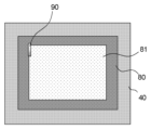
- FIG. 4 shows an example of the relationship between a substrate irradiation area 90 where the laser beam 4 is irradiated on the substrate 80 and an exposed region 81 on the substrate 80. As shown in FIG. 4, the substrate irradiation area 90 is smaller than the exposed region 81 on the substrate 80.
- the substrate irradiation area 90 shown in FIG. 4 is an area irradiated by one shot of the pulsed laser beam 4.
- the substrate irradiation area 90 corresponds to the mask irradiation area, which is a part of the effective area 22 of the mask 21, since the pattern is projected by the laser beam that has passed through the mask 21.
- the mask 21 is configured to be scanned along the sweep axes 21X and 21Y shown in FIG. 3.
- the substrate stage 40 is configured to be scanned along the sweep axes 80X and 80Y shown in FIG. 3.
- the exposure apparatus 100 of the present invention is configured to sweep and irradiate the mask 21 and the substrate stage 40 with the laser beam 4, and perform pattern exposure on the exposed area 81 of the substrate 80.
- the exposure apparatus 100 of the present invention is configured to perform overlapping irradiation (first embodiment) and/or to perform synchronous sweep irradiation with the laser beam irradiation position fixed (second embodiment), as described in detail below.
- the exposure apparatus 100 of the first aspect is configured to perform pattern exposure of an exposed region 81 of the substrate 80 by sweeping and irradiating the mask 20 and the substrate stage 80 while overlapping a portion of the substrate irradiation area 90 during exposure of the substrate 80.
- irradiating the laser beam while overlapping a portion of the substrate irradiation area 90 is referred to as overlapping irradiation.
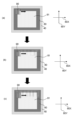
- FIG. 5(a) shows a substrate irradiation area 90 on a substrate 80 by one shot of a pulsed laser beam.
- the mask 20 and substrate stage 80 are swept, and the laser beam is irradiated so that the substrate irradiation area 91 of the first shot and the substrate irradiation area 92 of the second shot partially overlap in the direction of the arrow along the sweep axis 80X, as shown in FIG. 5(b).
- the laser beam is irradiated so that the substrate irradiation area 93 of the third shot partially overlaps with the substrate irradiation area 91 of the first shot and the substrate irradiation area 92 of the second shot.
- the exposure area expands along the sweep axis 80X.
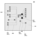
- FIG. 6(a) shows a process of pattern-exposing the first row of the exposed region 81 along the sweep axis 80X by the overlapping irradiation shown in FIG. 5(b).
- overlapping irradiation is performed along the sweep axis 80X so as to overlap a portion of the region overlapping-irradiated in FIG. 6(a) in the direction of the sweep axis 80Y (orthogonal to the sweep axis 80X), and the second row of the exposed region 81 is pattern-exposed along the sweep axis 80X.
- FIG. 6(b) shows a process of pattern-exposing the first row of the exposed region 81 along the sweep axis 80X by the overlapping irradiation shown in FIG. 5(b).
- overlapping irradiation is performed along the sweep axis 80X so as to overlap a portion of the region overlapping-irradiated in FIG. 6(a) and (b) in the direction of the sweep axis 80Y, and the third row of the exposed region 81 is pattern-exposed along the sweep axis 80X.
- the exposure region spreads over the exposed region 81.
- overlapping irradiation can be performed at regular intervals in the two directions of the sweep axes 80X and 80Y.
- the overlapping portions of the substrate irradiation area are irradiated with the laser beam multiple times.
- the portions receive sufficient pattern exposure according to the mask pattern shape, and the pattern exposure according to the mask pattern shape required for the exposed region 81 can be reliably achieved.
- a laser beam 4 which is a pulsed rectangular laser beam with uniform irradiation energy density and converted into an exposure shape through a mask 21, is irradiated onto a substrate irradiation area 90 of a substrate 80. Therefore, the exposure depth of the substrate irradiation area 90 in the substrate 80 corresponding to the mask irradiation area, which is a part of the effective area 22 of the mask 21, can be made uniform and irradiation can be performed multiple times. As a result, with this exposure apparatus 100, fine pattern exposure can be performed accurately across the exposed region 81 of the substrate 80.
- such an exposure device 100 does not require the use of high laser energy, can be constructed inexpensively without using expensive laser light sources or optical components, and can suppress deterioration of accuracy due to thermal drift of the laser beam, allowing for highly accurate pattern exposure.
- the exposure device 100 can irradiate the substrate with the laser beam 4 in a pulsed manner, so the overlapping irradiation can be performed at high speed.
- the exposure apparatus 100 can perform high-speed, high-precision pattern exposure.
- the exposure apparatus 100 according to the first aspect of the present invention, overlapping irradiation is performed, so the substrate irradiation area in one shot can be made smaller. As a result, high-density irradiation is possible.
- the second aspect of the exposure apparatus 100 is configured such that the mask 21 and the substrate stage 40 maintain a relative corresponding positional relationship by operating synchronously in a planar direction approximately perpendicular to the direction in which the laser beams 2 and 4 are irradiated.
- the mask 21 is configured such that the movement of the mask 21 along the sweep axis 21X is synchronized with the movement of the substrate stage 80 along the sweep axis 80X, and the movement of the mask 21 along the sweep axis 21Y is synchronized with the movement of the substrate stage 80 along the sweep axis 80Y, so that the mask 21 and the substrate stage 40 maintain a relative corresponding positional relationship.
- the second embodiment of the exposure apparatus 100 is also configured to, during exposure to the substrate 80, operate the mask 21 and the substrate stage 40 in synchronization with a fixed irradiation position of the laser beam 4, sweep-irradiate the mask 21 and the substrate stage 40, and perform pattern exposure of the exposed region 81 of the substrate 80.
- this type of sweep-irradiation that can be performed with the second embodiment of the exposure apparatus 100 will be referred to as "synchronous sweep-irradiation with a fixed irradiation position of the laser beam.”
- Such synchronous sweep irradiation allows pattern exposure to be performed with greater precision than when scanning a laser beam. Furthermore, with such an exposure device 100, a large-area mask can be used as the mask 21, and by using the large-area mask in combination with the third optical function unit 30, which will be described later, pattern exposure can be performed with a higher energy density.
- a laser beam 4 which is a pulsed and rectangular laser beam with uniform irradiation energy density and converted into an exposure shape through a mask 21, is irradiated onto a substrate irradiation area 90 of a substrate 80. Therefore, as in the first aspect, in the exposure apparatus 100 of the second aspect, multiple irradiations can be performed with a uniform exposure depth in the substrate irradiation area 90 in the substrate 80 corresponding to the mask irradiation area, which is a part of the effective area 22 of the mask 21. As a result, in this exposure apparatus 100, fine pattern exposure can be performed with high precision across the exposed region 81 of the substrate 80.
- such an exposure device 100 does not require the use of high laser energy, and can be constructed inexpensively without using expensive laser light sources or optical components. It is also possible to suppress deterioration of accuracy due to thermal drift of the laser beam, and to perform highly accurate pattern exposure. In addition, because small optical components can be used, inexpensive and highly accurate components can be used.
- the exposure device 100 of the first embodiment is preferably configured to perform synchronous sweep irradiation with the laser beam irradiation position fixed, in addition to the superimposed irradiation described above, as in the second embodiment.
- the laser beam 1 emitted from the laser light source 11 is preferably an excimer laser.
- Excimer lasers have a higher resolution due to their shorter wavelength compared to conventional solid-state lasers, such as LD-pumped solid-state (DPSS) lasers. Therefore, by using an excimer laser, more precise pattern exposure is possible. Also, for example, excimer lasers have very high absorption and high processing capabilities for epoxy-based substrate materials. Furthermore, excimer lasers have low coherency and are less likely to produce interference fringes, so they can form a very uniform flat-top beam pattern. This makes it possible to make the processing depth by ablation uniform.
- DPSS LD-pumped solid-state
- the shaping optical system 12 is preferably an optical system equipped with multiple cylindrical lenses, which shapes the laser beam 1 from the laser light source 11 into a laser beam having a rectangular irradiation shape and a uniform irradiation energy density, in particular a top-hat shaped laser beam.
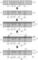
- Figure 7 shows a conceptual diagram of shaping the irradiation shape of a laser beam in a shaping optical system equipped with multiple cylindrical lenses.
- the shaping optical system 12 shown in FIG. 7 comprises a plurality of cylindrical lenses consisting of an X1 cylindrical lens 13, a Y1 cylindrical lens 14, an X2 cylindrical lens 15, and a Y2 cylindrical lens 16, and a focusing lens 17.
- the X1 cylindrical lens 13 and the X2 cylindrical lens 15 are arranged at a distance twice their focal length f1.
- the Y1 cylindrical lens 14 and the Y2 cylindrical lens 16 are also arranged at a distance twice their focal length.
- the laser beam 1 emitted by the laser light source 11 shown in FIG. 3 has a non-uniform irradiation shape (beam profile) as shown in FIG. 7.
- each component of the laser beam 1 is shaped according to their positions in the X and Y directions.
- the lower part of FIG. 7 shows, for example, a schematic diagram of the component indicated by "2" being shaped through cylindrical lenses 14 and 16.
- Each component of the laser beam 1 is shaped by the cylindrical lenses 13 to 16 and is focused at a position a focal length f2 away from the focusing lens 17.
- the laser beam 2 has a top hat beam shape, and is emitted from the shaping optical system 12 as outgoing light.
- the exposure apparatus 100 by performing overlapping irradiation using such a rectangular beam profile, there are no dead spots, which are areas that are not irradiated, and pattern exposure that is averaged within the tolerance range of the desired pattern exposure can be performed, making it possible to perform extremely efficient pattern exposure of the substrate 80.
- the second optical function section 20 further includes a mask stage that holds the mask 21 and sweeps the mask 21 . By attaching a sweep axis to the mask stage on which the mask 21 is held, the mask can be efficiently swept.
- correction can be easily made to the surface shape of the substrate 80 to be pattern exposed, making it possible to perform accurate pattern exposure.
- the second optical function section 20 can be configured to further shape the irradiation shape of the laser beam 2 that has passed through the first optical function section 10 through a mask 21 .
- the second optical function section 20 can further shape the irradiation shape of the laser beam 2 , which has been formed into a rectangular shape, according to a pattern corresponding to the exposed region 81 of the substrate 80 , for example.
- the mask 21 is installed in a direction approximately perpendicular to the horizontal plane on which the exposure device 100 is installed.
- the required resolution of the exposure pattern on the substrate is increasing, and distortion of the mask image affects the processing accuracy.
- the mask If the mask is installed in the same horizontal direction as the horizontal surface on which the equipment is installed, gravity will cause distortion and poor exposure accuracy if the mask is installed alone. Also, if the mask is made thicker to reduce bending, the mask will become very heavy, making it difficult to replace.
- the supports When inserting supports under the mask to prevent bending, the supports must be optically transparent, but as the mask becomes larger, the support material must be thicker, which not only creates cost problems but also increases the absorption of laser energy in the support material, reducing the energy efficiency of the laser irradiation.
- the optical path from the laser light source to the substrate is long, if the mask is placed horizontally, the height of the equipment becomes large. By placing the mask vertically, it becomes possible to lower the height of the equipment.
- the mask 21 if the mask 21 is placed in a direction approximately perpendicular to the horizontal surface on which the exposure device 100 is placed, the mask 21 will not bend and there is no need to use an optically transparent material to support it against bending, so the laser energy can be used efficiently and pattern exposure can be performed with high precision and extremely uniformity.
- the irradiation area of the laser beam 3 that has passed through the mask 21 can be reduced through an optional reduction optical system 31, which will be described below, to increase the energy density of the laser beam 4 that is irradiated onto the substrate. Therefore, even if the mask 21 is made large and has a large area, it is possible to achieve the desired fine pattern exposure by using a reduction optical system 31 that matches it.
- the size of the mask 21 is not particularly limited.
- a mask 21 can be used in which the dimensions in the vertical and horizontal directions perpendicular to the thickness direction are 700 mm or more (e.g., 700 mm x 800 mm) and the dimensions in the vertical and horizontal directions perpendicular to the thickness direction of the effective area 22 are 500 mm or more (e.g., 600 mm x 600 mm).
- hird optical function section 30 As in the exposure apparatus 100 shown in FIG. 3, it is preferable to further include a third optical function unit equipped with a reduction projection optical system 31 between the second optical function unit 20 and the substrate stage 40 .
- the exposure patterns on substrates have become finer, and the minimum width of the exposure pattern is now required to be several microns. This has an effect on minute dust particles, and minute dust particles that adhere to the mask portion in particular can cause a large amount of exposure failure. For this reason, the mask 21 is enlarged beyond the actual exposure, and the laser beam 3 that passes through the mask 21 is reduced and projected and exposed by the reduced projection optical system 31 at the subsequent stage, thereby minimizing the effect of minute dust particles.
- the energy of the laser beam 2 that strikes the mask 21 can be made smaller than the exposure energy. If the reduction ratio of the reduction projection optical system 31 is N, the energy of the laser beam that strikes the mask surface is 1/(N 2 ) compared to the exposure energy of the substrate 80 surface. This makes it possible to suppress thermal drift caused by the energy of the laser beam 2, thereby suppressing thermal expansion of the mask 21 and enabling highly accurate pattern exposure even after a long exposure operation.
- optical components e.g., the shaping optical system 12 and mask 21
- deterioration of optical components caused by the heat of the laser beam can be suppressed, thereby extending the lifespan of the optical components.
- the exposure apparatus 100 is configured to perform synchronous sweep irradiation with the laser beam irradiation position fixed, and can use a reduced projection lens with a very small aperture compared to a method in which the laser beam irradiation position is moved. This not only makes it cost-effective, but also reduces lens distortion and lens aberration, allowing for very high exposure precision of the substrate.
- the reduction projection optical system 31 can be equipped with a pair of reduction projection lenses.
- the magnification achieved by the reduction projection optical system 31 can be adjusted, for example, by the ratio of the focal lengths of the reduction projection lenses and the distance between the reduction projection lenses.
- the reduction projection lens preferably has a high NA (numerical aperture).
- NA number of apertures
- the exposure device of the present invention can perform projection exposure, and as a result, a reduction projection lens with a high NA can be used.
- the NA of the reduction projection lens is preferably selected to match the energy density required for pattern exposure of the substrate 80.
- the NA of the reduction projection lens is preferably 0.12 or more.
- the third optical function unit 30 further includes a cooling means for cooling the reduction projection optical system 31.
- the laser beam 3 that has passed through the mask 21 is reduced and projected at 1/N, so that the energy of the laser beam that passes through the lens portion at the tip of the objective becomes N2 times as much as the laser beam energy irradiated on the mask 21, and this portion is prone to heat influence. Therefore, by providing a cooling function to the reduction projection optical system 30 in order to suppress this heat energy, it is possible to suppress the thermal drift due to the energy of the laser beam, and it becomes possible to perform highly accurate pattern exposure even after a long exposure operation.
- the exposure apparatus 100 which is configured to perform synchronous sweep irradiation with the laser beam irradiation position fixed as described above, can use a reduction projection lens with a very small aperture.
- the cooling means for the reduction projection lens cannot be directly attached to the lens itself, but rather cools the jacket part that holds the lens. Therefore, if the lens aperture is large, although temperature control is possible around the periphery of the lens, the cooling effect is not as widespread around the crucial central part, making heat control difficult. For this reason, even a small amount of energy absorbed into the lens due to long-term laser beam irradiation can easily cause distortion due to heat. If the third optical function unit 30 has a cooling function, the lens aperture can be made small, thereby preventing such problems.
- the exposure apparatus 100 is configured to non-stop sweep the mask 21 and the substrate stage 40 while irradiating the mask 21 and the substrate stage 40 with pulsed laser beams 2 and 4, respectively, in a sweep irradiation in at least one direction.
- the exposure apparatus 100 of the present invention further includes an imaging means for reading characteristic portions of the substrate 80, an imaging means for reading characteristic portions of the mask 21, and an alignment mechanism for aligning the relative positions of the substrate and the mask based on positional information of the characteristic portions of the substrate and the mask.
- the exposure apparatus 100 shown in FIG. 3 includes a mask alignment camera 23 as an imaging means for reading characteristic portions of the mask 21, a substrate alignment camera 60 as an imaging means for reading characteristic portions of the substrate 80, and an alignment mechanism (not shown).
- the mask alignment camera 23 is configured to send position information of the characteristic portions of the mask 21 to the alignment mechanism.
- the substrate alignment camera 60 is configured to send position information of the characteristic portions of the substrate 80 to the alignment mechanism.
- the alignment mechanism is configured to adjust the relative positions of the substrate 80 and the mask 21 based on this position information.
- circuit boards are often processed across multiple layers, and if the exposure position of each layer for processing does not match the intended position precisely, the circuits on each layer will not connect, or even if they do connect, there will be high conductive resistance and other quality defects. To prevent this, the exposure position must be precise.
- the shape of the projected image of the pattern on the mask 21 is not necessarily exactly similar to the exposure shape on the substrate 80, and the magnification is not always the same due to the effects of thermal expansion and the like. Also, there are cases where it becomes necessary to deform the exposure shape on the substrate 80 relative to the projection image on the mask 21 due to minute distortions or deformations of the substrate 80.
- the positions of the mask 21 and the substrate 80 are acquired by imaging means (mask alignment camera 23 and substrate alignment camera 60), and the projected image of the mask 21 is aligned with the shape of the substrate to be exposed based on that information, enabling accurate pattern exposure onto the substrate.
- the projection position of the projection image of the mask 21 is acquired by the beam image detection camera 70, and correction is made based on the information of this projection position to optimize the projection magnification by the third optical function unit 30, and the sweep speed during sweep irradiation is also optimized based on the above information.
- This makes it possible to arbitrarily change the vertical and horizontal magnifications of the substrate 80 relative to the image of the mask 21 within a certain range, and to apply an optimal exposure shape to the resist film of the substrate.
- the exposure method of the first aspect of the present invention is a method of performing the overlapping irradiation described above using the exposure apparatus 100 of the first aspect. Therefore, according to the exposure method of the first aspect of the present invention, fine pattern exposure can be performed with high precision over the entire exposed region of the substrate. In addition, irradiation can be performed at a high energy density, and sufficient pattern exposure can be performed at high speed.
- the exposure method of the present invention is not limited to methods using the exposure apparatus 100 of the first aspect described above.
- the exposure method of the second aspect of the present invention is an exposure method for forming a printed wiring exposure pattern by exposing a resist film formed on the surface of a substrate to the irradiation energy of a laser beam, in which a rectangularly shaped laser beam is passed through a mask to irradiate the substrate with the laser beam so that the substrate irradiation area is smaller than the exposed region of the substrate, and when exposing the substrate, a portion of the substrate irradiation area is overlapped while performing pattern exposure of the exposed region of the substrate.
- the substrate is irradiated with a laser beam so that the substrate irradiation area is smaller than the exposed region of the substrate, and pattern exposure of the exposed region of the substrate is performed while overlapping a portion of the substrate irradiation area, i.e., overlapping irradiation is performed, so that fine pattern exposure can be performed with high precision over the exposed region of the substrate.
- the use of an excimer laser enables more precise pattern exposure.
- the exposure method of the third aspect of the present invention is a method of performing synchronous sweep irradiation with the previously described laser beam irradiation position fixed using the exposure apparatus 100 of the second aspect. Therefore, according to the exposure method of the third aspect of the present invention, fine pattern exposure can be performed with high precision over the exposed area of the substrate. Furthermore, according to the exposure method of the third aspect, pattern exposure can be performed with higher precision than when scanning a laser beam. Furthermore, with such an exposure method, a large area mask can be used as the mask 21, and by using a large area mask in combination with the previously described third optical function unit 30, pattern exposure can be performed with a higher energy density.
- an exposure apparatus 100 that satisfies one or more of the optional items described above.
- the sweep irradiation in at least one direction it is preferable to sweep the mask 21 and the substrate stage 40 non-stop while irradiating the mask 21 and the substrate stage 40 with pulsed irradiation of the laser beam 2 or 4, respectively.
- the exposure method of the first or third aspect of the present invention it is preferable to repeat the sweep irradiation multiple times for each exposure region 81 of the substrate 80.
- the depth that can be exposed in one sweep (one pass) is limited, and especially with the non-stop sweep exposure described above, it is not possible to irradiate the same exposed area multiple times.
- the exposure depth is averaged and it is possible to perform exposure to a uniform depth by shifting the substrate irradiation area 90 and shifting the irradiation for each sweep, for example, as described with reference to Figures 5 and 6.
- the characteristic parts of the substrate 80 can be read, for example, by a substrate alignment camera 60.
- the characteristic parts of the mask 21 can be read, for example, by a mask alignment camera 23.
- This type of exposure method allows for more accurate pattern exposure onto the substrate.
- Such correction can be performed, for example, by combining the third optical function unit 30, the beam image detection camera 70, the sweeping mechanism for the mask 21, and the sweeping mechanism for the substrate stage 80.
- Method of manufacturing a printed wiring board In the method for producing a printed wiring board of the present invention, a resist film formed on the surface of a substrate is subjected to pattern exposure by the exposure method of the present invention.
- this method of manufacturing printed wiring boards does not require the use of high laser energy, and can be constructed inexpensively without using expensive laser light sources or optical components. It also prevents deterioration of accuracy due to thermal drift of the laser beam, making it possible to manufacture boards on which pattern exposure has been performed with high accuracy.
- the area of the board irradiated in one shot can be made small, making high-density irradiation possible.
- the above-mentioned synchronous sweep irradiation is performed with the laser beam irradiation position fixed during the exposure operation on the board, so pattern exposure can be performed with higher accuracy than when scanning a laser beam. Furthermore, with such an exposure method, a large area mask can be used, so pattern exposure can be performed with a higher energy density.
- the method for manufacturing a printed wiring board of the present invention can be particularly advantageously applied to the manufacture of semiconductor packages.
- FIG. 8 shows a schematic flow diagram of a first embodiment of a method for producing a printed wiring board according to the present invention.
- a substrate 80 is prepared, which has a base substrate 80A and a resist film 80B formed on the surface of the base substrate 80A.
- the resist film 80B is subjected to pattern exposure using the exposure method of the present invention. As a result, an exposure pattern 80p consisting of exposed portions 80b is formed in the resist film 80B.
- the resist film 80B is developed to remove the exposed pattern 80p, and an opening 80H corresponding to the exposed pattern 80p is formed, as shown in FIG. 8(C).
- the resist film 80B having the opening 80H is used as a mask to process the base substrate 80A.
- the processing may be etching (wet or dry) or laser processing.
- etching wet or dry
- laser processing As a result, as shown in FIG. 8(D), for example, a recess (groove or trench) 80d and/or a through hole 80C can be formed in the base substrate 80A.
- a through electrode 80C can be formed in the through hole 80c, and an internal wiring 80D can be formed in the recess 80d. This results in the formation of a wiring pattern 80P consisting of the through electrode 80C and the internal wiring 80D.
- this is an example in which a wiring pattern 80P is formed on the surface of the substrate 80 after pattern exposure.
- an interlayer insulating film 80I may be formed on the surface of the substrate 80, for example as shown in FIG. 8(F).
- an electrode 80E may be formed at the end of the through electrode 80C, as shown in FIG. 8(F). This prevents short circuits due to electrical conduction between the internal wiring 80D and the outside, while enabling electrical connection between the through electrode 80C and the outside. This allows the manufacture of a printed wiring board 80F having the wiring pattern 80P.
- FIG. 9 shows an example of a printed wiring board 80F that can be manufactured using the printed wiring board manufacturing method of the present invention.
- the printed wiring board 80F includes a wiring pattern 80P consisting of a through electrode 80C and internal wiring 80D.
- the internal wiring 80D is covered with an interlayer insulating film 80I and is not exposed.
- the electrode E formed on the through electrode 80C is exposed.
- the blackened areas are the insertion ports for conductive terminals from the outside.
- the method for manufacturing a printed wiring board of the present invention allows for the precise formation of a fine exposure pattern, and therefore allows for the precise formation of a fine wiring pattern 80P based on such a fine exposure pattern.
- multiple internal wirings 80D can be formed between adjacent through electrodes 80C.
- FIG. 10 shows a schematic flow diagram of a second embodiment of the method for producing a printed wiring board according to the present invention.
- a through hole 80c and a recess 80d are formed in a base substrate 80A.
- the through hole 80c and the recess 80d can be formed, for example, by laser processing.
- a processing method in which the concept of overlapping irradiation according to the present invention is applied to laser processing can be used to process trenches and VIAs of any depth.
- a through electrode 80C is formed in the through hole 80c, and an internal wiring 80D is formed in the recess 80d.
- a wiring pattern 80P for example, consisting of the through electrode 80C and the internal wiring 80D.
- an interlayer insulating film 80I and a resist film 80B are formed in sequence on the surface of the base substrate 80A on which the wiring pattern 80P is formed.
- pattern exposure is performed using the exposure method of the present invention so that only the portions of the resist film 80B that correspond to the through electrodes 80C are exposed to light.
- an exposure pattern 80b consisting of exposed portions 80p is formed in the resist film 80B, as shown in FIG. 10(D).
- the resist film 80B is developed, the exposed pattern 80b is removed, and an opening corresponding to the exposed pattern 80b is formed. That is, in this example, after the wiring pattern 80P is formed on the surface of the substrate 80, the resist film 80B is formed on the surface of the substrate 80, and then the pattern exposure is performed.
- processing is performed to remove only the portion of the interlayer insulating film 80I directly above the through electrode 80C, forming an opening 80h.
- pattern exposure may be performed before forming the wiring pattern 80P on the surface of the substrate 80, or after forming the wiring pattern 80P on the surface of the substrate 80.
- the present invention is not limited to the above-described embodiments.
- the above-described embodiments are merely examples, and anything that has substantially the same configuration as the technical idea described in the claims of the present invention and exhibits similar effects is included within the technical scope of the present invention.
Landscapes
- Physics & Mathematics (AREA)
- General Physics & Mathematics (AREA)
- Exposure And Positioning Against Photoresist Photosensitive Materials (AREA)
- Engineering & Computer Science (AREA)
- Life Sciences & Earth Sciences (AREA)
- Health & Medical Sciences (AREA)
- Manufacturing & Machinery (AREA)
- Microelectronics & Electronic Packaging (AREA)
- Manufacturing Of Printed Circuit Boards (AREA)
- Atmospheric Sciences (AREA)
- Toxicology (AREA)
- Environmental & Geological Engineering (AREA)
- Epidemiology (AREA)
- Public Health (AREA)
- Sustainable Development (AREA)
- Optics & Photonics (AREA)
- Plasma & Fusion (AREA)
Priority Applications (6)
| Application Number | Priority Date | Filing Date | Title |
|---|---|---|---|
| JP2025514956A JPWO2024218897A1 (https=) | 2023-04-19 | 2023-04-19 | |
| PCT/JP2023/015608 WO2024218897A1 (ja) | 2023-04-19 | 2023-04-19 | プリント配線基板用露光装置、露光方法及びプリント配線基板の製造方法 |
| DE112023006228.5T DE112023006228T5 (de) | 2023-04-19 | 2023-04-19 | Belichtungsvorrichtung für ein substrat mit gedruckter verdrahtung, belichtungsverfahren und herstellungsverfahren für ein substrat mit gedruckter verdrahtung |
| CN202380097259.XA CN121002448A (zh) | 2023-04-19 | 2023-04-19 | 印刷配线基板用曝光装置、曝光方法、印刷配线基板的制造方法 |
| KR1020257038302A KR20260002933A (ko) | 2023-04-19 | 2023-04-19 | 프린트 배선 기판용 노광 장치, 노광 방법 및 프린트 배선 기판의 제조 방법 |
| TW113114084A TW202445282A (zh) | 2023-04-19 | 2024-04-16 | 印刷配線基板用曝光裝置、曝光方法、印刷配線基板的製造方法 |
Applications Claiming Priority (1)
| Application Number | Priority Date | Filing Date | Title |
|---|---|---|---|
| PCT/JP2023/015608 WO2024218897A1 (ja) | 2023-04-19 | 2023-04-19 | プリント配線基板用露光装置、露光方法及びプリント配線基板の製造方法 |
Publications (1)
| Publication Number | Publication Date |
|---|---|
| WO2024218897A1 true WO2024218897A1 (ja) | 2024-10-24 |
Family
ID=93152108
Family Applications (1)
| Application Number | Title | Priority Date | Filing Date |
|---|---|---|---|
| PCT/JP2023/015608 Ceased WO2024218897A1 (ja) | 2023-04-19 | 2023-04-19 | プリント配線基板用露光装置、露光方法及びプリント配線基板の製造方法 |
Country Status (6)
| Country | Link |
|---|---|
| JP (1) | JPWO2024218897A1 (https=) |
| KR (1) | KR20260002933A (https=) |
| CN (1) | CN121002448A (https=) |
| DE (1) | DE112023006228T5 (https=) |
| TW (1) | TW202445282A (https=) |
| WO (1) | WO2024218897A1 (https=) |
Citations (5)
| Publication number | Priority date | Publication date | Assignee | Title |
|---|---|---|---|---|
| JPH0933344A (ja) * | 1995-07-17 | 1997-02-07 | Canon Inc | 光量測定装置 |
| JPH09312255A (ja) * | 1996-05-23 | 1997-12-02 | Nikon Corp | 露光装置 |
| JP2001162392A (ja) * | 1999-09-28 | 2001-06-19 | Sumitomo Heavy Ind Ltd | レーザ穴あけ加工方法及び加工装置 |
| JP2007158225A (ja) * | 2005-12-08 | 2007-06-21 | Canon Inc | 露光装置 |
| JP2008053732A (ja) * | 2006-08-24 | 2008-03-06 | Asml Netherlands Bv | 露光装置及び露光方法 |
Family Cites Families (1)
| Publication number | Priority date | Publication date | Assignee | Title |
|---|---|---|---|---|
| JP2017132120A (ja) | 2016-01-27 | 2017-08-03 | 株式会社沖データ | 露光装置、画像形成装置及び露光装置製造方法 |
-
2023
- 2023-04-19 KR KR1020257038302A patent/KR20260002933A/ko active Pending
- 2023-04-19 DE DE112023006228.5T patent/DE112023006228T5/de active Pending
- 2023-04-19 JP JP2025514956A patent/JPWO2024218897A1/ja active Pending
- 2023-04-19 WO PCT/JP2023/015608 patent/WO2024218897A1/ja not_active Ceased
- 2023-04-19 CN CN202380097259.XA patent/CN121002448A/zh active Pending
-
2024
- 2024-04-16 TW TW113114084A patent/TW202445282A/zh unknown
Patent Citations (5)
| Publication number | Priority date | Publication date | Assignee | Title |
|---|---|---|---|---|
| JPH0933344A (ja) * | 1995-07-17 | 1997-02-07 | Canon Inc | 光量測定装置 |
| JPH09312255A (ja) * | 1996-05-23 | 1997-12-02 | Nikon Corp | 露光装置 |
| JP2001162392A (ja) * | 1999-09-28 | 2001-06-19 | Sumitomo Heavy Ind Ltd | レーザ穴あけ加工方法及び加工装置 |
| JP2007158225A (ja) * | 2005-12-08 | 2007-06-21 | Canon Inc | 露光装置 |
| JP2008053732A (ja) * | 2006-08-24 | 2008-03-06 | Asml Netherlands Bv | 露光装置及び露光方法 |
Also Published As
| Publication number | Publication date |
|---|---|
| CN121002448A (zh) | 2025-11-21 |
| JPWO2024218897A1 (https=) | 2024-10-24 |
| TW202445282A (zh) | 2024-11-16 |
| DE112023006228T5 (de) | 2026-02-26 |
| KR20260002933A (ko) | 2026-01-06 |
Similar Documents
| Publication | Publication Date | Title |
|---|---|---|
| US20080223839A1 (en) | Laser Machining Apparatus | |
| JP7278868B2 (ja) | レーザ加工装置 | |
| JP2025172783A (ja) | レーザ照射装置 | |
| WO2024218897A1 (ja) | プリント配線基板用露光装置、露光方法及びプリント配線基板の製造方法 | |
| JP7734754B2 (ja) | 加工装置、加工方法、基板の製造方法、及び半導体パッケージの製造方法 | |
| WO2024218894A1 (ja) | 加工装置、加工方法及び基板の製造方法 | |
| WO2024105861A1 (ja) | アブレーション加工方法、アブレーション加工装置、基板、及び基板を製造する方法 | |
| JP7732128B2 (ja) | レーザ照射装置、レーザ加工装置、レーザ加工方法、マスクの設置方法、レーザ加工装置の設置方法及びマスク | |
| TWI903099B (zh) | 照明光學系統以及雷射加工裝置 | |
| CN223414066U (zh) | 半导体封装基板 | |
| WO2026033742A1 (ja) | レーザ加工方法、半導体パッケージ基板の製造方法、及びレーザ加工装置 | |
| JP2023066566A (ja) | 照明光学系及びレーザ加工装置 | |
| TW202504715A (zh) | 雷射加工裝置以及雷射加工裝置之投影光學系統 | |
| CN116060799A (zh) | 照明光学系统和激光加工装置 |
Legal Events
| Date | Code | Title | Description |
|---|---|---|---|
| 121 | Ep: the epo has been informed by wipo that ep was designated in this application |
Ref document number: 23934043 Country of ref document: EP Kind code of ref document: A1 |
|
| ENP | Entry into the national phase |
Ref document number: 2025514956 Country of ref document: JP Kind code of ref document: A |
|
| WWE | Wipo information: entry into national phase |
Ref document number: 2025514956 Country of ref document: JP |
|
| WWE | Wipo information: entry into national phase |
Ref document number: CN202380097259X Country of ref document: CN |
|
| WWE | Wipo information: entry into national phase |
Ref document number: KR1020257038302 Country of ref document: KR |
|
| WWE | Wipo information: entry into national phase |
Ref document number: 112023006228 Country of ref document: DE |
|
| WWP | Wipo information: published in national office |
Ref document number: 112023006228 Country of ref document: DE |
|
| 122 | Ep: pct application non-entry in european phase |
Ref document number: 23934043 Country of ref document: EP Kind code of ref document: A1 |