WO2024214628A1 - 半導体装置及びその製造方法並びに電力変換装置 - Google Patents
半導体装置及びその製造方法並びに電力変換装置 Download PDFInfo
- Publication number
- WO2024214628A1 WO2024214628A1 PCT/JP2024/013915 JP2024013915W WO2024214628A1 WO 2024214628 A1 WO2024214628 A1 WO 2024214628A1 JP 2024013915 W JP2024013915 W JP 2024013915W WO 2024214628 A1 WO2024214628 A1 WO 2024214628A1
- Authority
- WO
- WIPO (PCT)
- Prior art keywords
- type
- heat sink
- dissipation fins
- heat dissipation
- semiconductor device
- Prior art date
- Legal status (The legal status is an assumption and is not a legal conclusion. Google has not performed a legal analysis and makes no representation as to the accuracy of the status listed.)
- Ceased
Links
Images















Classifications
-
- H—ELECTRICITY
- H05—ELECTRIC TECHNIQUES NOT OTHERWISE PROVIDED FOR
- H05K—PRINTED CIRCUITS; CASINGS OR CONSTRUCTIONAL DETAILS OF ELECTRIC APPARATUS; MANUFACTURE OF ASSEMBLAGES OF ELECTRICAL COMPONENTS
- H05K7/00—Constructional details common to different types of electric apparatus
- H05K7/20—Modifications to facilitate cooling, ventilating, or heating
-
- H—ELECTRICITY
- H10—SEMICONDUCTOR DEVICES; ELECTRIC SOLID-STATE DEVICES NOT OTHERWISE PROVIDED FOR
- H10W—GENERIC PACKAGES, INTERCONNECTIONS, CONNECTORS OR OTHER CONSTRUCTIONAL DETAILS OF DEVICES COVERED BY CLASS H10
- H10W40/00—Arrangements for thermal protection or thermal control
- H10W40/10—Arrangements for heating
-
- H—ELECTRICITY
- H10—SEMICONDUCTOR DEVICES; ELECTRIC SOLID-STATE DEVICES NOT OTHERWISE PROVIDED FOR
- H10W—GENERIC PACKAGES, INTERCONNECTIONS, CONNECTORS OR OTHER CONSTRUCTIONAL DETAILS OF DEVICES COVERED BY CLASS H10
- H10W40/00—Arrangements for thermal protection or thermal control
- H10W40/40—Arrangements for thermal protection or thermal control involving heat exchange by flowing fluids
- H10W40/43—Arrangements for thermal protection or thermal control involving heat exchange by flowing fluids by flowing gases, e.g. forced air cooling
-
- H—ELECTRICITY
- H10—SEMICONDUCTOR DEVICES; ELECTRIC SOLID-STATE DEVICES NOT OTHERWISE PROVIDED FOR
- H10W—GENERIC PACKAGES, INTERCONNECTIONS, CONNECTORS OR OTHER CONSTRUCTIONAL DETAILS OF DEVICES COVERED BY CLASS H10
- H10W90/00—Package configurations
Definitions
- the heat dissipation device includes a plurality of modular cooling devices having a heat dissipation plate on which heat generating elements are arranged, and a housing for removably connecting the plurality of modular cooling devices, the housing including an external frame, an opening formed to penetrate the interior of the external frame, and at least one bridge provided on the external frame to separate the opening and support the modular cooling device inserted into the opening.
- the heat dissipation device further includes at least one airflow direction guide member that is inserted between the plurality of modular cooling devices and controls the flow of air flowing into the interior of the modular cooling device.
- Conventional power semiconductor devices equipped with multiple power semiconductor modules generally employ a structure in which heat generated from the semiconductor elements in one power semiconductor module is dissipated by a heat sink. For this reason, when blowing cooling air to achieve a cooling function, the heated air flows into the heat sinks of the other power semiconductor modules, raising the temperatures of the semiconductor elements of the other power semiconductor modules. This characteristic is described in detail below.
- the air passing between the multiple heat dissipation fins directly below the heat sink on the windward side rises in temperature in order to dissipate heat generated by the power semiconductor module directly above.
- This heated air passes between the multiple heat dissipation fins directly below the heat sink on the downwind side.
- the temperature of the downwind air passing between the multiple heat dissipation fins directly below the heat sink on the downwind side is higher than the temperature of the upwind air passing between the multiple heat dissipation fins directly below the heat sink on the windward side. This reduces the effect of suppressing temperature rise in the power semiconductor module directly above the heat sink on the downwind side.
- This disclosure has been made to solve the above problems, and aims to provide a semiconductor device that has a cooling function for a semiconductor module and is compact in size.
- the semiconductor device disclosed herein is a semiconductor device including a first type heat sink, a second type heat sink, a first type semiconductor module mounted on the first type heat sink, and a second type semiconductor module mounted on the second type heat sink
- the first type heat sink has a plurality of first type heat dissipation fins, each of the plurality of first type heat dissipation fins having a first type formation depth extending in a formation depth direction on the side opposite to the mounting surface of the first type semiconductor module and a first type formation width extending in the fin formation direction
- the plurality of first type heat dissipation fins are arranged discretely from one another along a fin arrangement direction intersecting with the fin formation direction, and gap regions between the plurality of first type heat dissipation fins become first type cooling air passing regions
- the second type heat sink has a plurality of second type heat dissipation fins, each of the plurality of second type heat dissipation fins having a second type formation depth extending in the formation depth
- the semiconductor device has a cooling air supply structure that supplies cooling air to the first and second type heat sinks in a blowing direction along the fin formation direction, and the cooling air is supplied to pass through the second type cooling air passage area after passing through the first type cooling air passage area.
- the first type cooling air passage area includes multiple first type narrow areas and at least one first type wide area, and each of the multiple first type narrow areas has a first type narrow spacing, and the at least one first type wide area has a first type wide spacing.
- the second type cooling air passage area includes multiple second type width areas, and each of the multiple second type width areas has a second type spacing, and in the first type cooling air passage area, the first type wide spacing is set wider than the first type narrow spacing.
- the first type heat sink is on the windward side and the second type heat sink is on the leeward side of the cooling air supplied by the cooling air supply structure.
- the first type wide interval is set wider than the first type narrow interval.
- the semiconductor device disclosed herein can minimize the temperature rise of the cooling air passing through the first type wide region and allow the cooling air to flow into multiple second type heat dissipation fins.
- the semiconductor device disclosed herein can therefore suppress temperature rise in the multiple second-type heat dissipation fins in addition to the multiple first-type heat dissipation fins by the cooling air blown by the cooling air supply structure.
- the first-type heat sink can suppress temperature rise during operation of the first-type semiconductor module
- the second-type heat sink can suppress temperature rise during operation of the second-type semiconductor module.
- the semiconductor device disclosed herein does not require the first and second type semiconductor modules and the first and second type heat sinks to be enlarged in order to suppress temperature increases during operation of the first and second type semiconductor modules.
- the semiconductor device disclosed herein has a cooling function for the first and second types of semiconductor modules, and can also be made smaller.
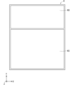
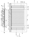
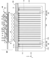
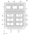
- FIG. 1 is an explanatory diagram illustrating a planar configuration of a semiconductor device according to a first embodiment of the present disclosure
- 2 is an explanatory diagram illustrating a planar structure of the heat sink mounting frame illustrated in FIG. 1
- FIG. 11 is an explanatory diagram illustrating a planar structure of a semiconductor device according to a modification of the first embodiment
- FIG. 1 is a cross-sectional view (part 1) illustrating a schematic cross-sectional structure of a power semiconductor module.
- FIG. 2 is a cross-sectional view (part 2) illustrating a schematic cross-sectional structure of the power semiconductor module;
- FIG. 4 is a cross-sectional view (part 3) illustrating a schematic cross-sectional structure of the power semiconductor module;
- FIG. 1 is a cross-sectional view (part 1) illustrating a schematic cross-sectional structure of a power semiconductor module.
- FIG. 2 is a cross-sectional view (part 2) illustrating a schematic cross-sectional structure of the power semiconductor module
- FIG. 1 is a first explanatory diagram illustrating a cross-sectional structure of a semiconductor device according to a first embodiment of the present invention
- FIG. 2 is an explanatory diagram (part 2) illustrating a schematic cross-sectional structure of the semiconductor device according to the first embodiment
- FIG. 1 is a first explanatory diagram illustrating a cross-sectional structure of a heat sink.
- FIG. 2 is a second explanatory diagram illustrating a cross-sectional structure of the heat sink.
- FIG. 4 is a third explanatory diagram illustrating a cross-sectional structure of the heat sink.
- 1 is an explanatory diagram (part 1) showing the effect of the semiconductor device of the first embodiment
- 11 is an explanatory diagram (part 2) showing the effect of the semiconductor device of the first embodiment;
- FIG. 1 is an explanatory diagram (part 1) showing the effect of the semiconductor device of the first embodiment
- 11 is an explanatory diagram (part 2) showing the effect of the semiconductor device of the first embodiment
- FIG. 11 is an explanatory diagram (part 3) showing the effect of the semiconductor device of the first embodiment;
- FIG. FIG. 11 is an explanatory diagram illustrating a planar configuration of a semiconductor device according to a second embodiment of the present invention;
- 11A to 11C are explanatory diagrams each showing a planar structure of a first type and a second type heat sink in a semiconductor device according to a second embodiment.
- 11 is an explanatory diagram illustrating a cross-sectional structure of a basic configuration of a semiconductor device according to a second embodiment of the present invention;
- 13 is an explanatory diagram illustrating a cross-sectional structure of a modified example of the semiconductor device according to the second embodiment;
- FIG. 13A to 13C are explanatory diagrams each showing a planar structure of a first type and a second type heat sink in a semiconductor device according to a third embodiment.
- 20 is an explanatory diagram illustrating a schematic cross-sectional structure of the semiconductor device illustrated in FIG. 19 .
- FIG. 13 is an explanatory diagram illustrating a planar configuration of a semiconductor device according to a fourth embodiment.
- FIG. 11 is an explanatory diagram (part 1) illustrating a schematic cross-sectional structure of a semiconductor device according to a fourth embodiment.
- FIG. 13 is an explanatory diagram (part 2) illustrating a schematic cross-sectional structure of a semiconductor device according to the fourth embodiment.
- 13 is an explanatory diagram (part 1) showing the effect of the semiconductor device of the fourth embodiment;
- FIG. 13 is an explanatory diagram (part 1) showing the effect of the semiconductor device of the fourth embodiment;
- FIG. 13 is an explanatory diagram illustrating a planar configuration of a semiconductor device that is a basic configuration of a fifth embodiment.
- 13 is an explanatory diagram illustrating a schematic cross-sectional structure of a semiconductor device according to a fifth embodiment.
- FIG. FIG. 2 is an explanatory diagram illustrating a cross-sectional structure of a heat sink-integrated power semiconductor module.
- 13 is an explanatory diagram (part 1) showing the effect of the semiconductor device of the fifth embodiment;
- FIG. FIG. 23 is an explanatory diagram (part 2) showing the effect of the semiconductor device of the fifth embodiment;
- FIG. 13 is an explanatory diagram illustrating a planar configuration of a semiconductor device that is a modification of the fifth embodiment
- FIG. 32 is an explanatory diagram illustrating a cross-sectional structure of FIG. 31 .
- 13 is an explanatory diagram (part 1) showing a basic manufacturing method of a semiconductor device according to a fifth embodiment
- FIG. FIG. 23 is an explanatory diagram (part 2) showing the basic manufacturing method of the semiconductor device according to the fifth embodiment
- FIG. 13 is an explanatory diagram (part 1) showing a first improved method for manufacturing a semiconductor device according to the fifth embodiment
- FIG. 23 is an explanatory diagram (part 2) showing the first improved manufacturing method of the semiconductor device of the fifth embodiment
- FIG. 1 is an explanatory diagram (part 1) showing a problem with the first improved manufacturing method.
- FIG. 1 is an explanatory diagram (part 1) showing a problem with the first improved manufacturing method.
- FIG. 2 is an explanatory diagram (part 2) showing the problem of the first improved manufacturing method.
- FIG. 13 is an explanatory diagram (part 1) showing a second improved method for manufacturing a semiconductor device according to the fifth embodiment;
- FIG. 23 is an explanatory diagram (part 2) showing the second improved manufacturing method of the semiconductor device of the fifth embodiment;
- FIG. 13 is an explanatory diagram (part 1) showing a third improved method for manufacturing a semiconductor device according to the fifth embodiment;
- FIG. 23 is an explanatory diagram (part 2) showing the third improved manufacturing method of the semiconductor device of the fifth embodiment;
- FIG. 13 is an explanatory diagram (part 1) showing a fourth improved method for manufacturing a semiconductor device according to the fifth embodiment;
- FIG. 13 is an explanatory diagram (part 1) showing a fourth improved method for manufacturing a semiconductor device according to the fifth embodiment;
- FIG. 13 is an explanatory diagram (part 1) showing a fourth improved method for manufacturing a semiconductor device according to the fifth embodiment;
- FIG. 13 is an explanatory diagram (part 1)
- FIG. 23 is an explanatory diagram (part 2) showing the fourth improved manufacturing method of the semiconductor device of the fifth embodiment
- FIG. 13 is a block diagram showing a configuration of a power conversion system to which a power conversion device according to a sixth embodiment is applied.
- 1 is an explanatory diagram illustrating a planar structure of a semiconductor device for comparison with the semiconductor device of the embodiment
- FIG. 1 is an explanatory diagram (part 1) that illustrates a schematic cross-sectional structure of a comparative semiconductor device.
- FIG. 13 is an explanatory diagram (part 2) that illustrates a cross-sectional structure of a comparative semiconductor device.
- FIG. 1 is an explanatory diagram (part 1) showing characteristics of a comparative semiconductor device
- FIG. 11 is an explanatory diagram (part 2) showing characteristics of a comparative semiconductor device;
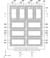
- ⁇ First embodiment> 1 is an explanatory diagram showing a schematic planar configuration of a semiconductor device 101 according to a first embodiment of the present disclosure.
- the semiconductor device 101 according to the first embodiment is a power semiconductor device having a plurality of power semiconductor modules.
- An XYZ orthogonal coordinate system is shown in FIG.
- an XYZ Cartesian coordinate system is used, with the upper surface on the +Z side being described as the first main surface, and the lower surface on the -Z side being described as the second main surface.
- the semiconductor device 101 of the first embodiment has a first type heat sink 5 and a second type heat sink 6, and the first and second type heat sinks 5 and 6 are attached to a heat sink mounting frame 4, which is an attachment plate.
- FIG. 2 is an explanatory diagram showing a schematic planar structure of the heat sink mounting frame 4.
- the XYZ Cartesian coordinate system is shown in FIG. 2.
- the heat sink mounting frame 4 has an opening K5 and an opening K6, and the first type heat sink 5 is attached so as to be fitted into the opening K5, and the second type heat sink 6 is attached so as to be fitted into the opening K6.
- the heat sink mounting frame 4 is fixed above the housing 3.
- the semiconductor device 101 of the first embodiment has six power semiconductor modules M11 to M16 mounted on the first main surface of the first-type heat sink 5, and three power semiconductor modules M41 to M43 mounted on the first main surface of the second-type heat sink 6.
- the semiconductor device 101 of the first embodiment has a plurality of power semiconductor modules, namely power semiconductor modules M11 to M16 and power semiconductor modules M41 to M43.
- the power semiconductor modules M11 to M16 are classified as first-type semiconductor modules, and the power semiconductor modules M41 to M43 are classified as second-type semiconductor modules. Therefore, the first main surface of the first-type heat sink 5 becomes the mounting surface for the first-type semiconductor modules, and the first main surface of the second-type heat sink 6 becomes the mounting surface for the second-type semiconductor modules.
- a cooling fan 2 is attached to the mounting side of the housing 3.
- a cooling fan 2 is used that blows cooling air with a flow velocity vector 1 in the air flow direction along the +Y direction. Note that with regard to the side of the housing 3, the side on the -Y direction opposite the +Y direction side on which the second type heat sink 6 is arranged relative to the first type heat sink 5 becomes the mounting side. In this way, the semiconductor device 101 realizes a cooling air supply structure that supplies cooling air in the air flow direction along the Y direction by using the cooling fan 2.
- Flow velocity vector 1 indicates the direction in which cooling air flows from cooling fan 2.
- cooling fan 2 takes in cooling air in the direction indicated by flow velocity vector 1, and supplies the cooling air to the multiple first-type heat dissipation fins and multiple second-type heat dissipation fins of first-type and second-type heat sinks 5 and 6, respectively, as described below.
- the first type heat sink 5 is located on the upwind side and the second type heat sink 6 is located on the downwind side of the cooling air supplied along flow velocity vector 1, which indicates the airflow direction.
- flow velocity vector 1 may also be in the direction of exhausting air from the housing 3. In other words, if the structure is such that the air flow matches flow velocity vector 1, a cooling air supply structure can be realized without using a cooling fan 2.
- the semiconductor device 101 of the first embodiment includes the power semiconductor modules M11 to M16, the power semiconductor modules M41 to M43, the first and second type heat sinks 5 and 6, the heat sink mounting frame 4, the housing 3, and the cooling fan 2 as main components.
- the heat sink mounting frame 4, which is the mounting plate, and the housing 3 are constructed as separate members, but the heat sink mounting frame 4 and the housing 3 may be constructed as a single unit by pressing, or the heat sink mounting frame 4 and the housing 3 may be constructed as an integrated part by welding, etc.
- FIG. 3 is an explanatory diagram showing a schematic planar structure of a semiconductor device 101s, which is a modification of the first embodiment.
- An XYZ orthogonal coordinate system is shown in FIG. 3.
- components similar to those of the semiconductor device 101 are given the same reference numerals and their description is omitted, and the following description focuses on the features of the modified semiconductor device 101s.
- the modified semiconductor device 101s has one power semiconductor module M1 mounted on the first main surface of the first-type heat sink 5, and one power semiconductor module M4 mounted on the first main surface of the second-type heat sink 6.
- the semiconductor device 101s of the modified example has a power semiconductor module M1 as a first type semiconductor module, and a power semiconductor module M4 as a second type semiconductor module. Therefore, the first main surface of the first type heat sink 5 becomes the mounting surface for the first type semiconductor module, and the first main surface of the second type heat sink 6 becomes the mounting surface for the second type semiconductor module.
- the number of heat sinks is "2" and the number of power semiconductor modules is "9", but in the semiconductor device 101s, which is a modified example of the first embodiment shown in FIG. 3, the number of heat sinks is "2" and the number of power semiconductor modules is "2".
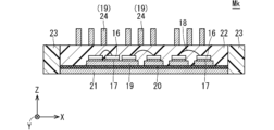
- Figures 4 to 6 are cross-sectional views that show the cross-sectional structures of power semiconductor modules Mi, Mj, and Mk. Each of Figures 4 to 6 shows an XYZ orthogonal coordinate system.
- An insulating material 20 is provided on a first main surface of a metal plate 21.
- a plurality of metal conductors 19 are selectively provided on the first main surface of the insulating material 20.
- a plurality of semiconductor elements 16 are selectively provided on the first main surfaces of the plurality of metal conductors 19 via bonding material 17. A portion of the spaces between the plurality of semiconductor elements 16, and the semiconductor elements 16 and the metal conductors 19 are electrically connected via wiring 18.
- the bonding material 17 is made of solder or the like, the multiple metal conductors 19 are provided using, for example, a lead frame, the insulating material 20 is made of, for example, an insulating sheet, and the sealing material 22 is made of, for example, an epoxy resin.
- the multiple semiconductor elements 16 may be Si-based semiconductor elements, SiC-based semiconductor elements, compound semiconductor elements such as GaN, etc., and are not particularly limited.
- a sealing material 22 is provided to cover the metal plate 21, the insulating material 20, the multiple metal conductors 19, the multiple bonding materials 17, the multiple semiconductor elements 16, and the multiple wirings 18.
- the insulating material 20, the multiple bonding materials 17, the multiple semiconductor elements 16, and the multiple wirings 18 are all sealed within the sealing material 22.
- the multiple metal conductors 19 are sealed within the sealing material 22, and some of them protrude from the first main surface or side surface of the sealing material 22 and are exposed to the outside. In addition, the second main surface of the metal plate 21 is exposed. Of the multiple metal conductors 19, the metal conductors 19 protruding from above the sealing material 22 are electrically connected to one of the multiple semiconductor elements 16.
- the power semiconductor module Mi having such a structure can be used as the power semiconductor modules M11 to M16 and the power semiconductor modules M41 to M43 of the semiconductor device 101, and can also be used as the power semiconductor module M1 and the power semiconductor module M4 of the semiconductor device 101s, which is a modified example.
- the exposed part of the metal conductor 19B protruding from the side of the sealing material 22 has a curved shape that includes a part parallel to the X direction and a part parallel to the Z direction.
- the power semiconductor module Mj having such a structure can be used as the power semiconductor modules M11 to M16 and the power semiconductor modules M41 to M43 of the semiconductor device 101, and can also be used as the power semiconductor module M1 and the power semiconductor module M4 of the semiconductor device 101s.
- a sealing material 22 is provided covering the metal plate 21, the insulating material 20, the multiple metal conductors 19, the multiple bonding materials 17, the multiple semiconductor elements 16, and the multiple wirings 18.
- the multiple bonding materials 17, the multiple semiconductor elements 16, and the multiple wirings 18 are all sealed within the sealing material 22.
- Some of the multiple metal conductors 19 are sealed within the sealing material 22, and some protrude from the first main surface of the sealing material 22 and are exposed to the outside as electrode terminals 24. In addition, the second main surface of the metal plate 21 is exposed.
- the resin case 23 contains inside it the metal plate 21, the insulating material 20, the multiple metal conductors 19, the multiple bonding materials 17, the multiple semiconductor elements 16, and the sealing material 22. At this time, the resin case 23 is in contact with the sides of the metal plate 21 and the insulating material 20.
- the power semiconductor module Mk having such a structure can be used as the power semiconductor modules M11 to M16 and the power semiconductor modules M41 to M43 of the semiconductor device 101, and can also be used as the power semiconductor module M1 and the power semiconductor module M4 of the semiconductor device 101s.
- power semiconductor modules other than the power semiconductor modules Mi, Mj, and Mk shown in Figures 4 to 6 can also be used as the first type semiconductor module or the second type semiconductor module for the semiconductor device 101 and the semiconductor device 101s.
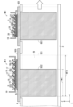
- FIGS. 7 and 8 are explanatory diagrams that show a schematic cross-sectional structure of the semiconductor device 101 of the first embodiment shown in FIG. 1.
- FIG. 7 shows the A-A cross section of FIG. 1
- FIG. 8 shows the B-B cross section of FIG. 1.
- An XYZ orthogonal coordinate system is shown in each of FIG. 7 and FIG. 8.
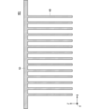
- the first type heat sink 5 has a heat sink base 51 and multiple heat dissipation fins 61.
- the multiple heat dissipation fins 61 are classified into multiple first type heat dissipation fins.
- Power semiconductor modules M13 and M14 are mounted on a first main surface of the heat sink base 51. Specifically, the second main surfaces of the metal plates 21 of the power semiconductor modules M13 and M14 are bonded to the first main surface of the heat sink base 51 via a TIM (Thermal Interface Material) material 25.
- the TIM material 25 is made of thermally conductive grease or the like, and ensures relatively high thermal conductivity between the first type heat sink 5 and the power semiconductor modules M13 and M14.
- the first main surface of the heat sink base 51 becomes the first main surface of the first type heat sink 5, and the multiple heat dissipation fins 61 each extend in the -Z direction from the second main surface of the heat sink base 51. Therefore, the multiple heat dissipation fins 61 each have a first type formation depth that extends in the formation depth direction (-Z direction) on the opposite side to the first main surface of the heat sink base 51, which is the mounting surface for the first type semiconductor module. In addition, the multiple heat dissipation fins 61 each have a first type formation width that extends in the fin formation direction along the Y direction.
- the multiple heat dissipation fins 61 are arranged in the X direction, which intersects at right angles with the Y direction, which is the fin formation direction, and the multiple heat dissipation fins 61 are arranged discretely from each other along the X direction, and the gap areas between the multiple heat dissipation fins 61 become multiple cooling air passage areas 91 or four cooling air passage areas 95.
- the assembly of the multiple cooling air passage areas 91 and the four cooling air passage areas 95 constitutes a first type cooling air passage area provided on the second main surface side of the first type heat sink 5.
- the multiple cooling air passage areas 91 are classified into multiple first type narrow areas, and the four cooling air passage areas 95 are classified into at least one first type wide area.
- the plurality of heat dissipating fins 61 each include four pairs of adjacent deformed heat dissipating fins 61X, 61X.
- the four pairs of deformed heat dissipating fins 61X, 61X are classified as at least one pair of deformed heat dissipating fins, and all other than the four pairs of deformed heat dissipating fins 61X, 61X are classified as normal heat dissipating fins 61n.
- the four cooling air passage regions 95 classified as at least one type 1 wide region correspond one-to-one to the four pairs of deformed heat dissipation fins 61X and 61X.
- Each of the four cooling air passage regions 95 is a gap region between a corresponding pair of deformed heat dissipation fins 61X and 61X among the four pairs of deformed heat dissipation fins 61X and 61X.
- Each of the four cooling air passage regions 95 has a wide fin spacing S5 along the X direction, which is the fin arrangement direction. This wide fin spacing S5 is classified as a type 1 wide spacing.
- the wide fin spacing S5 between the four pairs of modified heat dissipation fins 61X and 61X is dimensioned to be larger than the fin spacing S1 at the design level, not due to differences in the fin gaps caused by manufacturing variations.
- the heat dissipation fins 61 other than the four pairs of deformed heat dissipation fins 61X and 61X become multiple normal heat dissipation fins 61n.
- the multiple cooling air passing areas 91 are gap areas between adjacent normal heat dissipation fins 61n and 61n among the multiple normal heat dissipation fins 61n, and have a fin spacing S1 along the X direction. This fin spacing S1 is classified as a first type narrow spacing. Note that the fin spacing S1 is also set between adjacent normal heat dissipation fins 61n and deformed heat dissipation fins 61X.
- the spacing ratio (S5/S1) between the fin spacing S1 and the wide fin spacing S5 is set to, for example, about 2 to 3 times.
- the housing 3 supports the heat sink mounting frame 4 in a manner that accommodates a plurality of heat dissipation fins 61 of the first type heat sink 5.
- the heat sink base 51 of the first type heat sink 5 and the heat sink mounting frame 4 are fixed with screws or the like.
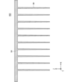
- the second type heat sink 6 has a heat sink base 52 and a plurality of heat dissipation fins 62.
- the plurality of heat dissipation fins 62 are classified into a plurality of second type heat dissipation fins.
- the power semiconductor modules M41 to M43 are mounted on the first main surface of the heat sink base 52.
- the second main surface of the metal plate 21 of each of the power semiconductor modules M41 to M43 is bonded to the first main surface of the heat sink base 52 via the TIM material 25, ensuring relatively high thermal conductivity between the second type heat sink 6 and the power semiconductor modules M41 to M43.
- the first main surface of the heat sink base 52 becomes the first main surface of the second-type heat sink 6, and the multiple heat dissipation fins 62 each extend in the -Z direction from the second main surface of the heat sink base 52. Therefore, the multiple heat dissipation fins 62 each have a second-type formation depth that extends in the formation depth direction (-Z direction) opposite the first main surface of the heat sink base 52, which is the mounting surface for the second-type semiconductor module. In addition, the multiple heat dissipation fins 62 each have a second-type formation width that extends in the fin formation direction along the Y direction.
- the multiple heat dissipation fins 62 are arranged in the X direction, which intersects at right angles with the Y direction, which is the fin formation direction, and the multiple heat dissipation fins 62 are arranged separately from each other along the X direction, and the gap areas between the multiple heat dissipation fins 62 become multiple cooling air passage areas 92.
- the assembly of the multiple cooling air passage areas 92 constitutes a second type cooling air passage area provided on the second main surface side of the second type heat sink 6.
- the multiple cooling air passage areas 92 are classified into multiple second type width areas.
- Each of the multiple cooling air passage areas 92 has a fin spacing S2 along the X direction, which is the fin arrangement direction.
- This fin spacing S2 is classified as a second type of width spacing.
- the fin spacing S2 is set, for example, to be approximately the same as the fin spacing S1 of the cooling air passage area 91 on the first type heat sink 5 side.
- the fin spacing S2 of the multiple heat dissipation fins 62 and 62 of the second type heat sink 6 placed on the downwind side is configured with a uniform fin spacing at the design level, excluding differences in fin spacing due to manufacturing variations.
- the spacing of the heat dissipation fins 62 and 62 of the second type heat sink 6 placed on the downwind side does not necessarily have to be a uniform fin spacing, and can be freely configured.
- the cooling air is blown from the cooling fan 2 along the flow velocity vector 1, so that the cooling air passes through the first type cooling air passage area below the first type heat sink 5, and then is supplied to pass through the second type cooling air passage area below the second type heat sink 6.
- the housing 3 supports the heat sink mounting frame 4 in a manner that accommodates a plurality of heat dissipation fins 62 of the second-type heat sink 6.
- the heat sink base 52 of the second-type heat sink 6 and the heat sink mounting frame 4 are fixed together with screws or the like.
- the cross-sectional structure of the modified semiconductor device 101s taken along line C-C in FIG. 3 is similar to the cross-sectional structure shown in FIG. 7, except that the first type semiconductor module mounted on the first main surface of the first type heat sink 5 is replaced by the power semiconductor module M1 instead of the power semiconductor modules M13 and M14.
- the cross-sectional structure of the semiconductor device 101s taken along line D-D in FIG. 3 is similar to the cross-sectional structure shown in FIG. 8, except that the second-type semiconductor module mounted on the first main surface of the second-type heat sink 6 is replaced with the power semiconductor module M4, replacing the power semiconductor modules M41-M43.
- Figures 9 to 11 are explanatory diagrams that show the cross-sectional structure of heat sinks HS1 to HS3. Each of Figures 9 to 11 shows an XYZ orthogonal coordinate system.
- the heat sink HS1 has a heat sink base 53 and a plurality of heat dissipation fins 63 provided on the second main surface side of the heat sink base 53.
- the heat sink HS1 is manufactured, for example, by extrusion processing.
- the heat sink HS1 shown in FIG. 9 may be used as the first type heat sink 5 and the second type heat sink 6. However, it is necessary to set the dimensions of the fin spacing S1 and the wide fin spacing S5 in the first type heat sink 5, and to set the dimension of the fin spacing S2 in the second type heat sink 6.
- the heat sink HS2 has a heat sink base 54 and a number of heat dissipation fins 64 provided on the second main surface side of the heat sink base 54.
- the number of heat dissipation fins 64 have a tapered structure along the formation depth direction, which is the -Z direction. In other words, the thickness, which is the formation width in the X direction, of each of the number of heat dissipation fins 64 becomes thinner along the depth direction.
- the heat sink HS2 shown in FIG. 10 may be used as the first type heat sink 5 and the second type heat sink 6. However, it is necessary to set the dimensions of the fin spacing S1 and the wide fin spacing S5 in the first type heat sink 5, and to set the dimension of the fin spacing S2 in the second type heat sink 6.
- the heat sink HS2 can be produced, for example, by casting (die casting). Aluminum, aluminum alloys, etc. are used as the constituent material of the heat sink HS1 and the heat sink HS2. However, the constituent material is not limited to aluminum material, and other constituent materials such as copper may also be used.
- the heat sink HS3 has a heat sink base 55 and a plurality of heat dissipation fins 65 provided on the second main surface side of the heat sink base 55.
- the heat sink HS3 shown in FIG. 11 may be used as the first type heat sink 5 and the second type heat sink 6. However, it is necessary to set the dimensions of the fin spacing S1 and the wide fin spacing S5 in the first type heat sink 5, and to set the dimension of the fin spacing S2 in the second type heat sink 6.
- the heat sink HS3 can be produced, for example, by casting (die casting). Aluminum, aluminum alloys, etc. are used as the constituent material of the heat sink HS3. However, the constituent material is not limited to aluminum material, and other constituent materials such as copper may also be used.
- the heat sink HS3 is a heat sink made by crimping, and the heat sink base 55 and multiple heat dissipation fins 65 are integrated by "crimping".
- the heat sink base 55 of the heat sink HS3 is made by cutting, die casting, forging, extrusion, etc., and aluminum and aluminum alloys are used as the constituent materials.
- the multiple heat dissipation fins 65 of the heat sink HS3 are made of plate material (rolled material) such as aluminum or aluminum alloy, so the multiple heat dissipation fins 65 can achieve both workability and heat dissipation properties.
- the constituent materials of the heat sink base 55 and the multiple heat dissipation fins 65 are not limited to the aluminum material described above, and may be a combination of different materials.
- the multiple heat dissipation fins 65 could be made of a copper-based plate material, which has a higher thermal conductivity than aluminum-based materials. In this case, the heat dissipation capacity can be improved compared to when the constituent material of the multiple heat dissipation fins 65 is an aluminum-based material.
- the heat sink structure used for the first type heat sink 5 and the second type heat sink 6 is not limited to the heat sinks HS1 to HS3 shown in Figures 9 to 11, and may be other heat sinks made by cutting, forging, etc.
- effect Comparative Technology Considerations
- FIGS. 46 to 48 are explanatory diagrams showing the structure of a comparative semiconductor device 201 for comparison with the semiconductor device 101 of the first embodiment.
- FIGS. 49 and 50 are explanatory diagrams showing the characteristics of the comparative semiconductor device 201.
- An XYZ orthogonal coordinate system is shown in each of FIGS. 46 to 50.
- Figure 46 is an explanatory diagram showing a schematic planar structure of the comparative semiconductor device 201.
- Figure 47 is an explanatory diagram showing a schematic E-E cross-sectional structure of Figure 46.
- Figure 48 is an explanatory diagram showing a schematic F-F cross-sectional structure of Figure 46.
- Figure 49 is an explanatory diagram showing the temperature distribution of air flowing between the heat dissipation fins of the heat sink of the comparative semiconductor device 201.
- Figure 50 is an explanatory diagram showing the temperature of air flowing into the heat sink of the comparative semiconductor device 201 in the form of a contour diagram. In Figure 50, the temperature distribution of the first type heat sink 7 is shown as air temperature contour TC2.
- the comparative semiconductor device 201 shown in Figures 46 to 50 is a power semiconductor device of a general structure that has multiple power semiconductor modules.
- the comparative semiconductor device 201 As shown in FIG. 46, in the comparative semiconductor device 201, six power semiconductor modules M11 to M16 are mounted on a first type heat sink 7, and three power semiconductor modules M41 to M43 are mounted on a second type heat sink 8.
- the first type heat sink 7 has a heat sink base 56 and a plurality of heat dissipation fins 66.
- the plurality of heat dissipation fins 66 are classified into a plurality of first type heat dissipation fins.
- Power semiconductor modules M13 and M14 are mounted on the first main surface of the heat sink base 56.
- the multiple heat dissipation fins 66 are arranged discretely from one another along the X direction, and the gap areas between the multiple heat dissipation fins 66 form multiple cooling air passage areas 98.
- the collection of the multiple cooling air passage areas 98 forms a first type cooling air passage area provided on the second main surface side of the first type heat sink 7.
- the cooling air passage areas 98 are gap areas between adjacent heat dissipation fins 66 in the heat dissipation fins 66, and have a fin spacing S8 along the X direction. This fin spacing S8 is classified as a first type of width spacing.
- the housing 3 supports the heat sink mounting frame 4 in a manner that accommodates a number of heat dissipation fins 66 of the first type heat sink 7.
- the heat sink base 56 of the first type heat sink 7 and the heat sink mounting frame 4 are fixed together with screws or the like.
- the fin spacing S8 between adjacent fins 66 of the first type heat sink 7 arranged on the windward side is configured to be uniform at the design level, excluding differences in fin spacing due to manufacturing variations.
- the fin spacing S8 is set to be approximately the same as the fin spacing S1 in the first type heat sink 5 of the semiconductor device 101, for example.
- the second type heat sink 8 has a heat sink base 57 and multiple heat dissipation fins 67.
- the multiple heat dissipation fins 67 are classified as multiple second type heat dissipation fins.
- Power semiconductor modules M41 to M43 are mounted on the first main surface of the heat sink base 57.
- the multiple heat dissipation fins 67 are arranged discretely from each other along the X direction, and the gap areas between the multiple heat dissipation fins 67 form multiple cooling air passage areas 94.
- the assembly of the multiple cooling air passage areas 94 becomes a second type cooling air passage area provided on the second main surface side of the second type heat sink 8.
- the multiple cooling air passage areas 94 are classified into multiple second type width areas.
- Each of the multiple cooling air passage areas 94 has a fin spacing S4 along the X direction, which is the fin arrangement direction.
- This fin spacing S4 is classified as a second type of width spacing.
- the fin spacing S4 between adjacent fins 67 of the multiple heat dissipation fins 67 of the second type heat sink 8 arranged on the downwind side is configured with a uniform fin spacing at the design level, excluding differences in fin spacing due to manufacturing variations.
- the fin spacing S4 is set to be approximately the same as the fin spacing S1 in the first type heat sink 5 of the semiconductor device 101 and the fin spacing S8 in the first type heat sink 7, for example.
- the housing 3 supports the heat sink mounting frame 4 in a manner that accommodates a number of heat dissipation fins 67 of the second-type heat sink 8.
- the heat sink base 57 of the second-type heat sink 8 and the heat sink mounting frame 4 are fixed together with screws or the like.
- the multiple semiconductor elements 16 in each of the power semiconductor modules M11 to M16 generate heat, and the multiple semiconductor elements 16 in each of the power semiconductor modules M41 to M43 also generate heat.
- heat generated from the multiple semiconductor elements 16 in each of the power semiconductor modules M11 and M12 is dissipated from the first type heat sink 7 directly below, causing the temperature of the cooling air flowing into each of the power semiconductor modules M13 and M14 to rise.
- heat generated from the multiple semiconductor elements 16 in each of the power semiconductor modules M13 and M14 is dissipated from the first type heat sink 7 directly below, further increasing the temperature of the cooling air flowing into each of the power semiconductor modules M15 and M16.
- heat generated by the multiple semiconductor elements 16 in each of the power semiconductor modules M15 and M16 is dissipated from the first-type heat sink 7 directly below, further increasing the temperature of the cooling air flowing into each of the power semiconductor modules M41 to M43.
- the width in the X direction of each of the air flow velocity vectors F1 to F3 shown in Figure 49 indicates the amount of heat. As shown in Figure 49, in the comparative semiconductor device 201, the amount of heat of the air flow velocity vector F3 before it reaches the second type heat sink 8 is quite large.
- the second-type heat sink 8 cannot suppress the temperature rise of the multiple semiconductor elements 16 in each of the power semiconductor modules M41 to M43, which causes the power semiconductor modules M41 to M43 to reach a high temperature state.
- the comparative semiconductor device 201 has the problem that the temperature of the cooling air flowing into the second type heat sink 8 becomes quite high, as shown in Figure 50. Note that in Figure 50, the higher the air temperature, the darker the black color becomes.
- power semiconductor modules M11 to M16 and the power semiconductor modules M41 to M43 are generally referred to as "power semiconductor modules MP.”
- a typical comparative semiconductor device 201 air is mainly introduced and exhausted from the inlet and outlet sides, with very little air being introduced and exhausted from sides other than the inlet and outlet sides.
- IP International Protection
- FIGS. 12 to 14 are explanatory diagrams showing the cooling effect of the semiconductor device 101 according to the first embodiment.
- An XYZ orthogonal coordinate system is depicted in each of Figs.
- FIG. 12 is an explanatory diagram showing the temperature distribution of the air flowing between the heat dissipation fins of the heat sink of the semiconductor device 101.
- FIGS. 13 and 14 are explanatory diagrams showing the temperature of the air flowing into the heat sink of the semiconductor device 101 in the form of a contour diagram, with FIG. 13 showing the temperature distribution of the first type heat sink 5 as an air temperature contour TC1, and FIG. 14 showing the temperature distribution of the first type heat sink 5 and the second type heat sink 6 as an air temperature contour TC1B. Note that in each of FIGS. 13 and 14, the higher the air temperature, the darker the black becomes.
- the first type heat sink 5 in the semiconductor device 101 of the first embodiment has four pairs of modified heat dissipation fins 61X and 61X.
- the four cooling air passage areas 95 which are the gap areas between the four modified heat dissipation fins 61X and 61X, each have a wide fin spacing S5, and this wide fin spacing S5 is set wider than the fin spacing S1. Therefore, during operation, the semiconductor device 101 can effectively suppress the temperature rise of the cooling air when it reaches the multiple heat dissipation fins 62 of the second type heat sink 6.
- heat generated by the multiple semiconductor elements 16 in each of the power semiconductor modules M11 and M12 is dissipated from the first type heat sink 5 directly below, causing the temperature of the cooling air that flows into the power semiconductor modules M13 and M14 to rise.
- heat generated from the multiple semiconductor elements 16 in each of the power semiconductor modules M13 and M14 is dissipated from the first-class heat sink 5 directly below, causing the temperature of the cooling air flowing into the power semiconductor modules M15 and M16 to rise. Furthermore, heat generated from the multiple semiconductor elements 16 in each of the power semiconductor modules M15 and M16 is dissipated from the first-class heat sink 5 directly below, causing the temperature of the air flowing into the power semiconductor modules M41 to M43 to rise.
- each of the air flow velocity vectors F1 to F3 and the air flow velocity vector FX1 shown in FIG. 12 indicates the amount of heat.
- the amount of heat of the air flow velocity vector F3 before it reaches the second type heat sink 6 is quite large.
- the wide fin spacing S5 in the four cooling air passage areas 95 is set to be larger than the fin spacing S1 in the multiple cooling air passage areas 91.
- the temperature rise of the cooling air along the flow velocity vector 1 in the four cooling air passage areas 95 can be kept to a minimum. This is because, in a cooling air passage area 95 having a relatively wide wide fin spacing S5, the coefficient of heat transfer from the surface of the deformed heat dissipation fin 61X to the air is small and the amount of heat dissipation from the deformed heat dissipation fin 61X is small, so the amount of rise in the air temperature of the cooling air passing through the cooling air passage area 95 is negligible.
- the four cooling air passage areas 95 can be kept in a relatively low temperature area tc11, as shown in Figures 13 and 14.
- the amount of heat is kept below a certain value, so that cooling air having a relatively low temperature air flow velocity vector FX can be supplied to the second type heat sink 6.
- a relatively low temperature region tc12 can be provided even in the second type heat sink 6 on the downwind side (air outlet side), so the temperature of the multiple semiconductor elements 16 in each of the power semiconductor modules M41 to M43 can be kept below the allowable temperature without increasing the size of the first type heat sink 5 and the second type heat sink 6.
- the size of the first type heat sink 5 and the second type heat sink 6 can be kept to a minimum, making it possible to miniaturize the semiconductor device 101 of the first embodiment.
- the first type heat sink 5 is on the windward side and the second type heat sink 6 is on the leeward side with respect to the cooling air supplied from the cooling fan 2.
- the first type heat sink 5 in the semiconductor device 101 of the first embodiment has four cooling air passing areas 95, each set to a wide fin spacing S5, so that the temperature rise of the cooling air passing through the cooling air passing areas 95 classified as the first type wide areas can be minimized, and relatively low-temperature cooling air can be allowed to flow into the multiple heat dissipation fins 62 of the second type heat sink 6.
- the semiconductor device 101 of the first embodiment can suppress the temperature rise of the multiple heat dissipation fins 62 in addition to the multiple heat dissipation fins 61 by the cooling air blown from the cooling fan 2. Therefore, the first type heat sink 5 can suppress the temperature rise of the power semiconductor modules M11 to M16 during operation, and the second type heat sink 6 can suppress the temperature rise of the power semiconductor modules M41 to M43 during operation.
- the semiconductor device 101 of the first embodiment in order to suppress the temperature rise during operation of the power semiconductor modules M11 to M16 and M41 to M43, there is no need to increase the size of the power semiconductor modules M11 to M16 and M41 to M43, as well as the first type heat sink 5 and the second type heat sink 6.
- the semiconductor device 101 of the first embodiment has a cooling function for the power semiconductor module MP by the first type heat sink 5 and the second type heat sink 6, and can achieve miniaturization of the device.
- the heat dissipation properties of the second type heat sink 6 can be maintained good.
- the semiconductor device 101 of the first embodiment has a configuration in which four cooling air passage areas 95 are set by four pairs of modified heat dissipation fins 61X and 61X, so that the temperature rise of the cooling air passing through the four cooling air passage areas 95 can be minimized and the cooling air can be made to flow into the multiple heat dissipation fins 62 of the second type heat sink 6.
- the semiconductor device 101 of the first embodiment has a cooling function by the first type heat sink 5 and the second type heat sink 6, and can achieve miniaturization of the device.
- cooling air passage areas 95 are shown as at least one first type wide area, but the above-mentioned effect can be achieved if there is at least one cooling air passage area 95.
- the semiconductor device 101 of the first embodiment includes a heat sink mounting frame 4, which is a mounting plate, and a housing 3, and includes a cooling fan 2 that blows cooling air with the flow velocity vector 1 as the blowing direction to realize a cooling air supply structure.
- the semiconductor device 101 of the first embodiment can obtain a structure in which the first type heat sink 5, the second type heat sink 6, the power semiconductor modules M11 to M16, and the power semiconductor modules M41 to M43 are integrated by the heat sink mounting frame 4 and the housing 3.
- the cooling fan 2 can then stably supply cooling air having a flow velocity vector 1.
- the semiconductor device 101 of the first embodiment can be manufactured by the following steps (a) to (c).
- Step (a) is a step of fixing the heat sink mounting frame 4, which serves as a mounting plate, to the housing 3.
- Step (b) is a step of mounting the first type heat sink 5 and the second type heat sink 6 on the heat sink mounting frame 4 in a manner that accommodates multiple heat dissipation fins 61 and multiple heat dissipation fins 62 within the housing 3.
- Step (c) is a step of mounting the power semiconductor modules M11 to M16 on the first main surface of the first type heat sink 5, and mounting the power semiconductor modules M41 to M43 on the first main surface of the second type heat sink 6.
- the semiconductor device 101 manufactured by the semiconductor device manufacturing method of the first embodiment does not need to be enlarged in order to suppress the temperature rise during operation of the power semiconductor modules M11-M16 and M41-M43, and the first and second type heat sinks 5 and 6.
- the semiconductor device 101 manufactured by the manufacturing method of the first embodiment has a cooling function for the power semiconductor modules M11 to M16 and M41 to M43, and can also be made smaller.
- Fig. 15 is an explanatory diagram showing a schematic planar configuration of a semiconductor device 102 according to a second embodiment of the present disclosure.
- An XYZ orthogonal coordinate system is shown in Fig. 15.
- the semiconductor device 102 according to the second embodiment is a power semiconductor device having a plurality of power semiconductor modules.
- the semiconductor device 102 of the second embodiment has a first type heat sink 5B and a second type heat sink 6B, and the first and second type heat sinks 5B and 6B are attached to the heat sink mounting frame 4, which is a mounting plate, in the same manner as in the first embodiment.
- the semiconductor device 102 of the second embodiment has six power semiconductor modules M11 to M16 mounted on the first main surface of the first-type heat sink 5B, and three power semiconductor modules M41 to M43 mounted on the second main surface of the second-type heat sink 6B.
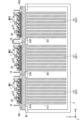
- FIG. 16 is an explanatory diagram showing a schematic planar structure of the first and second type heat sinks 5B and 6B in the semiconductor device 102 of the second embodiment.
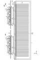
- FIG. 17 is an explanatory diagram showing a schematic cross-sectional structure in the basic configuration of the semiconductor device 102.
- FIG. 17 shows the G-G cross-sectional structure of FIG. 16.
- An XYZ orthogonal coordinate system is shown in each of FIG. 16 and FIG. 17.
- Figure 16 shows the planar structure of the multiple heat dissipation fins provided on the first type heat sink 5B and the multiple heat dissipation fins provided on the second type heat sink 6B so that they can be visually recognized.
- the first type heat sink 5B includes a heat sink base 5B0, a plurality of normal heat dissipation fins 5B1, and four notched heat dissipation fins 5B2, while the second type heat sink 6B includes a heat sink base 6B0 and a plurality of heat dissipation fins 6B1.
- the gap areas between adjacent normal heat dissipation fins 5B1 among the multiple normal heat dissipation fins 5B1 become multiple cooling air passing areas 91, and the spacing along the X direction, which is the fin arrangement direction of the cooling air passing areas 91, becomes the fin spacing S1.
- the multiple cooling air passing areas 91 are classified into multiple first type narrow areas, and the fin spacing S1 is classified into the first type narrow spacing.
- the four notched heat dissipation fins 5B2 are classified into at least one notched heat dissipation fin.
- a pair of normal heat dissipation fins 5B1 adjacent in the X direction which is the fin arrangement direction, are defined as four pairs of adjacent heat dissipation fins 5B1s and 5B1s.
- the four pairs of adjacent heat dissipation fins 5B1s and 5B1s are classified into at least one pair of adjacent heat dissipation fins.
- each of the four notched heat dissipation fins 5B2 has a normal region R51 with a normal depth DT1 in the -Z direction, which is the formation depth direction, and a deformed region R52 with a deformed depth DT2.
- each of the multiple normal heat dissipation fins 5B1 has only a constant normal depth DT1.
- the notched heat dissipation fin 5B2 includes the normal depth DT1 and the modified depth DT2 as the first type forming depth, and the normal heat dissipation fin 5B1 has only the normal depth DT1 as the first type forming depth.
- the deformation depth DT2 is shallower than the normal depth DT1, ⁇ DT1 > DT2 ⁇ holds. Therefore, in the notched heat dissipation fin 5B2, the area from the deformation depth DT2 of the deformation region R52 to the normal depth DT1 becomes the partial cutout region 27 where nothing is formed. In other words, the partial cutout region 27 that becomes the cutout region is the empty area from the deformation depth DT2 to the normal depth DT1 in the deformation region R52 of each of the four notched heat dissipation fins 5B2.
- the gap areas between each of the four pairs of adjacent heat dissipation fins 5B1s and 5B1s become four cooling air passage areas 96, which are classified as at least one first type wide area.
- Each of the four cooling air passage areas 96 includes an area between the adjacent heat dissipation fins 5B1s and 5B1s via a partial cutout area 27.
- the spacing between each of the four pairs of adjacent heat dissipation fins 5B1s and 5B1s in the X direction is the wide fin spacing S6.
- This wide fin spacing S6 is classified as the first type of wide spacing.
- the first-type heat sink 5B has a group of multiple cooling air passage areas 91 and four cooling air passage areas 96 as the first-type cooling air passage area.
- the first type heat sink 5B in the semiconductor device 102 of the second embodiment has four notched heat dissipation fins 5B2.
- Four pairs of adjacent heat dissipation fins 5B1s and four cooling air passage areas 96 including gap areas through the partial cutout areas 27 of 5B1s each have a wide fin spacing S6, which is set wider than the fin spacing S1. Therefore, when the semiconductor device 102 is in operation, the temperature rise of the cooling air supplied from the cooling fan 2 when it reaches the multiple heat dissipation fins 6B1 can be effectively suppressed.
- the multiple heat dissipation fins including the multiple normal heat dissipation fins 5B1 and the four notched heat dissipation fins 5B2, are arranged with a uniform fin spacing S1. Therefore, in the semiconductor device 102 of the second embodiment, the fin spacing S6 of the cooling air passage area 96 is twice the fin spacing S1 plus the thickness, which is the formation width in the X direction, of the notched heat dissipation fins 5B2.
- the semiconductor device 102 of the second embodiment has the structure shown in Figures 15 to 17, so that the temperature rise of the cooling air passing through the cooling air passage area 96, which includes the area through the partial cutout area 27 between each of the four pairs of adjacent heat dissipation fins 5B1s and 5B1s, can be minimized and the cooling air can be made to flow into the multiple heat dissipation fins 6B1.
- the semiconductor device 102 of the second embodiment has a cooling function for the power semiconductor modules M11 to M16 and the power semiconductor modules M41 to M43, and can achieve a compact device.
- the empty area from the deformation depth DT2 to the normal depth DT1 of each of the four notched heat dissipation fins 5B2 is the partial cutout area 27.
- four cooling air passage areas 96 can be formed from a general structure in which the spacing between multiple heat dissipation fins, including multiple normal heat dissipation fins 5B1 and four notched heat dissipation fins 5B2, is set to a uniform fin spacing S1.
- the basic configuration of the semiconductor device 102 shown in Figures 15 to 17 is such that the four notched heat dissipation fins 5B2 are formed in a combination of a deformation region R52 with a deformation depth DT2 and a normal region R51 with a normal depth DT1 in order to provide a partial cutout region 27.
- FIG. 18 is a cross-sectional view showing a schematic cross-sectional structure of a modified example of semiconductor device 102.
- FIG. 18 shows the G-G cross-sectional structure of FIG. 16.
- the XYZ orthogonal coordinate system is shown in FIG. 18.
- the modified example of semiconductor device 102 will be described, focusing on the differences from the cross-sectional structure of the basic configuration of semiconductor device 101 shown in FIG. 17.
- the first type heat sink 5BB in the modified example includes a heat sink base 5B0, a number of normal heat dissipation fins 5B1, and four notched heat dissipation fins 5B3.
- the four notched heat dissipation fins 5B3 are classified into at least one notched heat dissipation fin.
- the normal heat dissipation fins 5B1 and 5B1 adjacent in the X direction which is the fin arrangement direction, are defined as four pairs of adjacent heat dissipation fins 5B1s and 5B1s.
- the four pairs of adjacent heat dissipation fins 5B1s and 5B1s are classified into at least one pair of adjacent heat dissipation fins.
- each of the multiple normal heat dissipation fins 5B1 has a normal depth DT1.
- each of the four notched heat dissipation fins 5B3 is composed only of a deformation region R53 having a deformation depth DT2. Therefore, the first type forming depth in the notched heat dissipation fins 5B3 is only the shape depth DT2.
- the deformation depth DT2 is shallower than the normal depth DT1, ⁇ DT1 > DT2 ⁇ holds. Therefore, in the notched heat dissipation fin 5B3, the area from the deformation depth DT2 to the normal depth DT1 in the deformation region R53 becomes the notched region 28 where nothing is formed. In other words, the notched region 28 becomes the empty area from the deformation depth DT2 to the normal depth DT1 in the deformation region R53 which is the entire area of each of the four notched heat dissipation fins 5B3.
- the gap areas between each of the four pairs of adjacent heat dissipation fins 5B1s and 5B1s become the four cooling air passage areas 96 in the modified example, and are classified as at least one first type wide area.
- Each of the four cooling air passage areas 96 includes an area via the cutout area 28 between the adjacent heat dissipation fins 5B1s and 5B1s.
- the spacing along the X direction between each of the four pairs of adjacent heat dissipation fins 5B1s and 5B1s becomes the wide fin spacing S6, and is classified as the first type wide spacing.
- the modified example of the semiconductor device 102 of the second embodiment has the configuration shown in Figures 15, 16, and 18, so that the cooling air can be made to flow into the multiple heat dissipation fins 6B1 while minimizing the temperature rise of the cooling air passing through the cooling air passage area 96, which includes the area through the notch area 28 between each of the four pairs of adjacent heat dissipation fins 5B1s and 5B1s.
- the modified example of the semiconductor device 102 of the second embodiment has the same cooling function for the power semiconductor modules M11 to M16 and the power semiconductor modules M41 to M43 as the basic configuration of the second embodiment, and can also achieve a reduction in the size of the device.
- the empty area from the deformation depth DT2 to the normal depth DT1 of each of the four notched heat dissipation fins 5B3 is defined as the notched area 28.
- four cooling air passage areas 96 can be formed from a general structure in which the spacing between multiple heat dissipation fins, including multiple normal heat dissipation fins 5B1 and four notched heat dissipation fins 5B3, is set to a uniform fin spacing S1.
- the basic configuration of the semiconductor device 102 is such that the four notched heat dissipation fins 5B3 are formed with only a deformation region R53 of deformation depth DT2 in order to provide the notched region 28.
- the cutout region 28 of the modified example can be easily created compared to the cutout region 27 of the basic configuration.
- Fig. 19 is an explanatory diagram showing a schematic planar structure of the first and second type heat sinks 5C and 6C in the semiconductor device 103 of the embodiment 3.
- Fig. 20 is an explanatory diagram showing a schematic H-H cross-sectional structure of the semiconductor device 103 in Fig. 19. An XYZ orthogonal coordinate system is shown in each of Figs. 19 and 20.
- Figure 19 shows the planar structure of the multiple heat dissipation fins provided on the first type heat sink 5C and the multiple heat dissipation fins provided on the second type heat sink 6C so that they can be visually recognized.
- the semiconductor device 103 of the third embodiment is characterized by having a first type heat sink 5C and a second type heat sink 6C.
- the planar configuration of the semiconductor device 103 is the same as that of the semiconductor device 101 of the first embodiment, except that the first and second type heat sinks 5 and 6 are replaced with the first and second type heat sinks 5C and 6C.
- the first type heat sink 5C includes a heat sink base 5C0, a plurality of normal heat dissipation fins 5C1, and four notched heat dissipation fins 5C2, while the second type heat sink 6C includes a heat sink base 6C0 and a plurality of heat dissipation fins 6C1.
- the gap area between adjacent normal heat dissipation fins 5C1 and 5C1 among the multiple normal heat dissipation fins 5C1 is the cooling air passage area 91, and the distance along the X direction, which is the fin arrangement direction of the cooling air passage area 91, is the fin spacing S1.
- the cooling air passage area 91 is classified as a first type narrow area
- the fin spacing S1 is classified as a first type narrow spacing.
- the four notched heat dissipation fins 5C2 are classified into at least one notched heat dissipation fin.
- the normal heat dissipation fins 5C1 and 5C1 adjacent in the X direction which is the fin arrangement direction, are defined as four pairs of adjacent heat dissipation fins 5C1s and 5C1s.
- the four pairs of adjacent heat dissipation fins 5C1s and 5C1s are classified into at least one pair of adjacent heat dissipation fins.
- the multiple normal heat dissipation fins 5C1 each have a normal width WT1 in the Y direction, which is the fin formation direction, and the four notched heat dissipation fins 5C2 each have a deformed width WT2 in the Y direction, where the deformed width WT2 is shorter than the normal width WT1, satisfying ⁇ WT2 ⁇ WT1 ⁇ .
- the notched heat dissipation fin 5C2 of the semiconductor device 102 of embodiment 3 has the feature that the first type formation width includes the normal width WT1 and the deformed width WT2, and the deformed width WT2 is narrower than the normal width WT1.
- the empty area from the deformed width WT2 to the normal width WT1 of each of the four notched heat dissipation fins 5C2 is the notched area 29.
- the non-fin formation area where the normal heat dissipation fins 5C1 exist and the notched heat dissipation fins 5C2 do not exist is the notched area 29.
- the gap area between each of the four pairs of adjacent heat dissipation fins 5C1s and 5C1s becomes a cooling air passage area 97, which is classified as at least one first type wide area.
- the spacing along the X direction between each of the four pairs of adjacent heat dissipation fins 5C1s and 5C1s becomes a fin spacing S7, which is classified as a first type wide spacing.
- Each of the four cooling air passage areas 97 includes an area through the cutout area 29 between the adjacent heat dissipation fins 5C1s and 5C1s.
- the assembly of the multiple cooling air passage areas 91 and the four cooling air passage areas 97 constitutes the first type cooling air passage area.
- the first type heat sink 5B in the semiconductor device 103 of the third embodiment has four notched heat dissipation fins 5C2.
- the four cooling air passage areas 97 including the gap areas through the four pairs of adjacent heat dissipation fins 5C1s and the notched areas 28 of the 5C1s, each have a wide fin spacing S7, and this fin spacing S7 is set wider than the fin spacing S1. Therefore, during operation, the semiconductor device 103 can effectively suppress the temperature rise of the cooling air supplied from the cooling fan 2 to the multiple heat dissipation fins 6C1.
- the multiple heat dissipation fins including the multiple normal heat dissipation fins 5C1 and the four notched heat dissipation fins 5C2, are arranged with a uniform fin spacing S1. Therefore, in the semiconductor device 103 of the third embodiment, the fin spacing S7 is twice the fin spacing S1 plus the thickness of the notched heat dissipation fins 5C2.
- the semiconductor device 103 of the third embodiment has the structure shown in FIG. 19 and FIG. 20, so that the cooling air can be made to flow into the multiple heat dissipation fins 6C1 while minimizing the temperature rise of the cooling air passing through the four cooling air passage areas 97, each of which includes the area through the notch area 29 between each of the four pairs of adjacent heat dissipation fins 5C1s and 5C1s.
- the semiconductor device 103 of the third embodiment has a cooling function for the power semiconductor modules M11 to M16 and the power semiconductor modules M41 to M43, and can achieve a compact device.
- the non-fin regions of each of the four notched heat dissipation fins 5C2 are defined as notched regions 29.
- four cooling air passage areas 97 can be formed from a general structure in which the spacing between multiple heat dissipation fins, including multiple normal heat dissipation fins 5C1 and four notched heat dissipation fins 5C2, is set to a uniform fin spacing S1.
- ⁇ Fourth embodiment> 21 is an explanatory diagram showing a schematic planar configuration of a semiconductor device 104 according to a fourth embodiment of the present disclosure.
- the semiconductor device 104 according to the fourth embodiment is a power semiconductor device having a plurality of power semiconductor modules.
- An XYZ orthogonal coordinate system is shown in FIG.
- the semiconductor device 104 of the fourth embodiment has first-type heat sinks H51 to H56 and second-type heat sinks H61 to H64, and the first and second-type heat sinks 5 and 6 are attached to a heat sink mounting frame 4D, which is an attachment plate.
- the semiconductor device 104 of embodiment 4 has multiple first-type heat sinks H51 to H56 as first-type heat sinks, and multiple second-type heat sinks H61 to H64 as second-type heat sinks.
- the heat sink mounting frame 4D has six openings and four openings (not shown), and the first type heat sinks H51 to H56 are attached by fitting into each of the six openings, and the second type heat sinks H61 to H64 are attached by fitting into each of the four openings.
- the heat sink mounting frame 4D is fixed to the top of the housing 3.
- the first main surface of each of the first type heat sinks H51 to H56 serves as a mounting surface for a first type semiconductor module
- the first main surface of each of the second type heat sinks H61 to H64 serves as a mounting surface for a second type semiconductor module.
- the first type heat sinks H51 to H56 are located on the windward side, and the second type heat sinks H61 to H64 are located on the leeward side.
- the semiconductor device 104 of the fourth embodiment includes the power semiconductor modules M51 to M56, the power semiconductor modules M61 to M64, the first type heat sinks H51 to H56, the second type heat sinks H61 to H64, the heat sink mounting frame 4D, the housing 3, and the cooling fan 2 as main components.
- FIGS. 22 and 23 are explanatory diagrams that show a schematic cross-sectional structure of the semiconductor device 104 of the fourth embodiment shown in FIG. 21.
- FIG. 22 shows the I-I cross section of FIG. 21, and
- FIG. 23 shows the J-J cross section of FIG. 21.
- An XYZ orthogonal coordinate system is shown in each of FIG. 22 and FIG. 23.
- the first type heat sink H53 has a heat sink base 530 and multiple heat dissipation fins 531
- the first type heat sink H54 has a heat sink base 540 and multiple heat dissipation fins 541.
- the multiple heat dissipation fins 531 and the multiple heat dissipation fins 541 are classified as multiple first type heat dissipation fins.
- a power semiconductor module M53 is mounted on the first main surface of the first type heat sink H53, and a power semiconductor module M54 is mounted on the first main surface of the first type heat sink H54.
- the first type heat sink H53 has the same structure as each of the first type heat sinks H51, H52, H54 to H56, and the power semiconductor module M53 has the same structure as each of the power semiconductor modules M51, M52, M54 to M56.
- the following description will be given using the first type heat sink H53 and the power semiconductor module M53 as representative examples.
- the heat sink base 530 corresponds to the heat sink base 540
- the multiple heat dissipation fins 531 correspond to the multiple heat dissipation fins 541 (541n, 541X).
- the second main surface of the metal plate 21 of the power semiconductor module M53 is bonded to the first main surface of the first type heat sink H53 via the TIM material 25.
- the TIM material 25 By using the TIM material 25, a relatively high thermal conductivity is ensured between the first type heat sink H53 and the power semiconductor module M53.
- the first main surface of the heat sink base 530 becomes the first main surface of the first type heat sink H53, and the multiple heat dissipation fins 531 each extend in the -Z direction from the second main surface of the first type heat sink H53. Therefore, the multiple heat dissipation fins 531 each have a first type formation depth that extends in the formation depth direction (-Z direction) on the opposite side to the first main surface of the first type heat sink H53, which is the mounting surface for the first type semiconductor module. In addition, the multiple heat dissipation fins 531 each have a first type formation width that extends in the fin formation direction along the Y direction.
- the multiple heat dissipation fins 531 are arranged in the X direction, which intersects at right angles with the Y direction, which is the fin formation direction, and the multiple heat dissipation fins 531 are arranged separately from each other along the X direction, and the gap areas between the multiple heat dissipation fins 531 become multiple cooling air passage areas 111 or two cooling air passage areas 115.
- the assembly of the multiple cooling air passage areas 111 and the two cooling air passage areas 115 constitutes a first type cooling air passage area provided on the second main surface side of the first type heat sink H53.
- the multiple cooling air passage areas 111 are classified into multiple first type narrow areas, and the two cooling air passage areas 115 are classified into at least one first type wide area.
- the plurality of heat dissipating fins 531 each include two adjacent pairs of modified heat dissipating fins 531X and 531X.
- the two pairs of modified heat dissipating fins 531X and 531X are classified as at least one pair of modified heat dissipating fins, and all heat dissipating fins 531 other than the two pairs of modified heat dissipating fins 531X, 531X are classified as a plurality of normal heat dissipating fins 531n.
- the two cooling air passage regions 115 are classified as at least one first type wide region and correspond one-to-one to the two pairs of deformed heat dissipation fins 531X and 531X.
- the two cooling air passage regions 115 are the gap regions between the corresponding pairs of deformed heat dissipation fins 531X and 531X of the two pairs of deformed heat dissipation fins 531X and 531X.
- the two cooling air passage regions 115 each have a wide fin spacing S15 along the X direction, which is the fin arrangement direction. This wide fin spacing S15 is classified as a first type wide spacing.
- the wide fin spacing S15 between the two pairs of modified heat dissipation fins 531X and 531X is dimensioned to be larger than the fin spacing S11 at the design level, not due to differences in the fin gaps caused by manufacturing variations.
- the cooling air passage areas 111 are gap areas between adjacent normal heat dissipation fins 531n and 531n among the normal heat dissipation fins 531n, and have a fin spacing S11 along the X direction. This fin spacing S11 is classified as a first type narrow spacing.
- the spacing ratio (S15/S11) between the fin spacing S11 and the wide fin spacing S15 is set to, for example, about 2 to 3 times.
- the housing 3 supports the heat sink mounting frame 4D in a manner that accommodates the multiple heat dissipation fins 531 of the first type heat sink H53 and the multiple heat dissipation fins 541 of the first type heat sink H54.
- the heat sink base 530 of the first type heat sink H53 and the heat sink mounting frame 4D are fixed with screws or the like.
- the J-J cross-sectional structure in Figure 21 actually includes second-type heat sinks H61-H64 and power semiconductor modules M61-M64, but for ease of explanation, Figure 23 selectively shows second-type heat sinks H61-H63 and power semiconductor modules M61-M63.
- the second type heat sink H61 has a heat sink base 610 and multiple heat dissipation fins 611
- the second type heat sink H62 has a heat sink base 620 and multiple heat dissipation fins 621
- the second type heat sink H63 has a heat sink base 630 and multiple heat dissipation fins 631.
- the multiple heat dissipation fins 631, the multiple heat dissipation fins 621, and the multiple heat dissipation fins 631 are classified as multiple second type heat dissipation fins.
- a power semiconductor module M61 is mounted on the first main surface of the second type heat sink H61, a power semiconductor module M62 is mounted on the first main surface of the second type heat sink H62, and a power semiconductor module M63 is mounted on the first main surface of the second type heat sink H63.
- the second type heat sink H61 has the same structure as each of the second type heat sinks H62 to H64, and the power semiconductor module M61 has the same structure as each of the power semiconductor modules M62 to M64.
- the following description will be given using the second type heat sink H61 and the power semiconductor module M61 as representative examples.
- the heat sink base 610, the heat sink base 620, and the heat sink base 630 correspond to each other, and the multiple heat dissipation fins 611, the multiple heat dissipation fins 621, and the multiple heat dissipation fins 631 correspond to each other.
- the power semiconductor module M61 is mounted on the first main surface of the heat sink base 610. That is, the second main surface of the metal plate 21 of the power semiconductor module M61 is bonded to the first main surface of the heat sink base 610 via the TIM material 25, and the TIM material 25 ensures relatively high thermal conductivity between the second type heat sink H61 and the power semiconductor module M61.
- the first main surface of the heat sink base 610 becomes the first main surface of the second type heat sink H61, and the multiple heat dissipation fins 611 each extend in the -Z direction from the second main surface of the heat sink base 610. Therefore, the multiple heat dissipation fins 611 each have a second type formation depth that extends in the formation depth direction (-Z direction) on the opposite side to the first main surface of the heat sink base 610, which is the mounting surface for the second type semiconductor module. In addition, the multiple heat dissipation fins 611 each have a second type formation width that extends in the fin formation direction along the Y direction.
- the multiple heat dissipation fins 611 are arranged in the X direction, which is the fin formation direction, and the multiple heat dissipation fins 611 are arranged separately from each other along the X direction, and the gap areas between the multiple heat dissipation fins 611 become multiple cooling air passage areas 121.
- the assembly of the multiple cooling air passage areas 121 constitutes a second type cooling air passage area provided on the second main surface side of the second type heat sink H61.
- the multiple cooling air passage areas 121 are classified into multiple second type width areas.
- Each of the multiple cooling air passage areas 121 has a fin spacing S21 along the X direction, which is the fin arrangement direction.
- This fin spacing S21 is classified as a second type of width spacing.
- the fin spacing S21 is set, for example, to be approximately the same as the fin spacing S11 of the cooling air passage area 111 on the first type heat sink H53 side.
- the fin spacing S21 of the multiple heat dissipation fins 611 of the second type heat sink H61 arranged on the downwind side is configured with uniform fin spacing at the design level, excluding differences in fin spacing due to manufacturing variations.
- the spacing between the heat dissipation fins 611 and 611 of the second type heat sink H61 arranged on the downwind side does not necessarily have to be uniform fin spacing, and can be freely configured.
- the housing 3 supports the heat sink mounting frame 4D in a manner that accommodates the multiple heat dissipation fins 611, multiple heat dissipation fins 621, and multiple heat dissipation fins 631 of the second type heat sinks H61 to H63.
- the heat sink base 610 of the second type heat sinks H61 to H63 and the heat sink mounting frame 4D are fixed with screws or the like.
- FIGS. 24 and 25 are explanatory diagrams showing the cooling effect of the semiconductor device 104 according to the fourth embodiment.
- An XYZ orthogonal coordinate system is shown in each of Figs. 24 and 25.
- Figure 24 is an explanatory diagram showing the temperature distribution of air flowing between the heat dissipation fins of the heat sink of the semiconductor device 104.
- Figure 25 is an explanatory diagram showing the temperature of air flowing into the first type heat sinks H51 to H56 of the semiconductor device 104 in the form of a contour diagram, and Figure 25 shows the temperature distribution of the first type heat sinks H51 to H56 as air temperature contour TC4.
- the first type heat sink H53 in the semiconductor device 104 of the fourth embodiment has two pairs of modified heat dissipation fins 531X and 531X.
- the two cooling air passage areas 115 which are the gap areas between the two pairs of modified heat dissipation fins 531X and 531X, each have a wide fin spacing S15, and this wide fin spacing S15 is set wider than the fin spacing S11 of the cooling air passage area 111. Therefore, during operation of the semiconductor device 104, the temperature rise of the cooling air when it reaches the multiple heat dissipation fins 61 of the second type heat sink H61 can be effectively suppressed.
- heat generated by the multiple semiconductor elements 16 in each of the power semiconductor modules M51 and M52 is dissipated from the first type heat sinks H51 and H52, respectively, causing the temperature of the air flowing into the power semiconductor modules M53 and M54 to rise.
- heat generated from the multiple semiconductor elements 16 in each of the power semiconductor modules M53 and M54 is dissipated from the first-type heat sinks H53 and H54, respectively, causing the temperature of the air flowing into the power semiconductor modules M55 and M56 to rise.
- heat generated from the multiple semiconductor elements 16 in each of the power semiconductor modules M55 and M56 is dissipated from the first-type heat sinks H55 and H56, respectively, causing the temperature of the air flowing into the power semiconductor modules M61 to M64 to rise.
- the cooling air which is air with a raised temperature due to heat generated by the multiple semiconductor elements 16 in each of the power semiconductor modules M51 to M56 mounted on the first type heat sinks H51 to H56 on the windward side, flows into the second type heat sinks H61 to H64 on the leeward side on which the power semiconductor modules M61 to M64 are mounted.
- each of the air flow velocity vectors F11 to F13 and the air flow velocity vector FX1 shown in FIG. 24 indicates the amount of heat.
- the amount of heat of the air flow velocity vector F13 before it reaches the second type heat sinks H61 to H64 is quite large.
- the wide fin spacing S15 between the two pairs of modified heat dissipation fins 531X and 531X among the multiple heat dissipation fins 531 is set to be larger than the fin spacing S11 between the adjacent normal heat dissipation fins 531n and 531n.
- the two cooling air passage areas 115 can be kept at a relatively low temperature area tc41, as shown in FIG. 25. Note that in FIG. 15, the higher the air temperature, the darker the black color becomes.
- a relatively low temperature region can be provided in the second type heat sinks H61 to H64 on the leeward side, so the temperature of the multiple semiconductor elements 16 in each of the power semiconductor modules M61 to M64 can be kept below the allowable temperature without increasing the size of the first type heat sinks H51 to H56 and the second type heat sinks H61 to H64.
- the size of the first type heat sinks H51 to H56 and the second type heat sinks H61 to H64 can be reduced to the minimum necessary, thereby enabling miniaturization of the semiconductor device 104 of embodiment 4.
- the first type heat sinks H51 to H56 are on the windward side and the second type heat sinks H61 to H64 are on the leeward side with respect to the cooling air supplied from the cooling fan 2.
- Each of the first type heat sinks H51 to H56 in the semiconductor device 104 of embodiment 4 has two cooling air passing areas 115 set at a wide fin spacing S15. This allows the cooling air to flow into the multiple heat dissipation fins 611 of the second type heat sinks H61 to H64 while minimizing the temperature rise of the cooling air passing through the cooling air passing areas 115 classified as the first type wide areas.
- the wide fin spacing S15 is set to be between two and three times the fin spacing S11 ⁇ 2 ⁇ (S15/S11) ⁇ 3 ⁇ , similar to the spacing ratio (S5/S1) described in embodiment 1, a beneficial effect of suppressing the temperature rise of the cooling air can be obtained.
- the semiconductor device 104 of the fourth embodiment can suppress the temperature rise of the multiple heat dissipation fins 611, etc., in addition to the multiple heat dissipation fins 531, etc., by the cooling air blown from the cooling fan 2. Therefore, the first type heat sinks H51 to H56 can suppress the temperature rise of the power semiconductor modules M51 to M56 during operation, and the second type heat sinks H61 to H64 can suppress the temperature rise of the power semiconductor modules M61 to M64 during operation.
- the semiconductor device 104 of the fourth embodiment in order to suppress the temperature rise during operation of the power semiconductor modules M51-M56 and M61-M64, there is no need to increase the size of the power semiconductor modules M51-M56 and M61-M64, as well as the first type heat sinks H51-H56 and the second type heat sinks H61-H64.
- the semiconductor device 104 of the fourth embodiment has a cooling function for the power semiconductor module MP by the first type heat sinks H51 to H56 and the second type heat sinks H61 to H64, and can achieve a compact device.
- the semiconductor device 104 of the fourth embodiment has a structure including first type heat sinks H51-H56 and power semiconductor modules M51-M56 in one-to-one correspondence, and second type heat sinks H61-H64 and power semiconductor modules M61-M64 in one-to-one correspondence, which allows the device to be made compact.
- the structure of the plurality of heat dissipation fins 531, etc. is the same as the structure of the plurality of heat dissipation fins 61 of the first embodiment shown in FIG. 7, but is not limited to this structure.
- the structure of the plurality of heat dissipation fins 531, etc. may be a structure including the plurality of normal heat dissipation fins 5B1 and four notched heat dissipation fins 5B2 (5B3) of the second embodiment shown in FIGS. 16 to 18, or a structure including the plurality of normal heat dissipation fins 5C1 and four notched heat dissipation fins 5C2 shown in FIGS. 19 and 20.
- first type heat sinks H51 to H56 are described as being on the windward side, and the second type heat sinks H61 to H64 are described as being on the leeward side, but this classification is not limiting.
- ⁇ Fifth embodiment> 26 is an explanatory diagram showing a schematic planar configuration of a semiconductor device 105 which is a basic configuration of the fifth embodiment of the present disclosure.
- the semiconductor device 105 of the fifth embodiment is a power semiconductor device having a plurality of power semiconductor modules.
- An XYZ orthogonal coordinate system is shown in FIG.
- the semiconductor device 105 which is the basic configuration of the fifth embodiment, has heatsink-integrated power semiconductor modules HM51-HM56 and heatsink-integrated power semiconductor modules HM61-HM64.
- the heatsink-integrated power semiconductor modules HM51-HM56 and HM61-HM64 are attached to a heatsink mounting frame 4D, which is an attachment plate.
- the semiconductor device 105 of embodiment 5 has heat sink portions HK51 to HK56 as multiple first-type heat sinks, and has heat sink portions HK61 to HK64 as multiple second-type heat sinks.
- the heat sink mounting frame 4D has six openings and four openings (not shown), and the heat sink integrated power semiconductor modules HM51 to HM56 are attached by fitting into each of the six openings, and the heat sink integrated power semiconductor modules HM61 to HM64 are attached by fitting into each of the four openings.
- the heat sink mounting frame 4D is fixed to the top of the housing 3.
- the first main surface of each of the heat sink portions HK51 to HK56 becomes the mounting surface for the first type semiconductor module
- the first main surface of each of the heat sink portions HK61 to HK64 becomes the mounting surface for the second type semiconductor module.
- the heat sink integrated power semiconductor modules HM51 to HM56 are located on the windward side with respect to the flow velocity vector 1, and the heat sink integrated power semiconductor modules HM61 to HM64 are located on the leeward side.
- the semiconductor device 105 of the fifth embodiment includes the heat sink integrated power semiconductor modules HM51 to HM56, the heat sink integrated power semiconductor modules HM61 to HM64, the heat sink mounting frame 4D, the housing 3, and the cooling fan 2 as main components.
- the power semiconductor module parts MM51 to MM56 and the power semiconductor module parts MM61 to MM64 each have the cross-sectional structure shown in, for example, Figures 4 to 6.
- the heat sink mounting frame 4D, which is the mounting plate, and the housing 3 may be configured as separate members or as an integrated part.
- FIG. 27 is an explanatory diagram showing a schematic cross-sectional structure of the semiconductor device 105 of the fifth embodiment shown in FIG. 26.
- FIG. 27 shows the K-K cross section of FIG. 26.
- the L-L cross-sectional structure of FIG. 26 is omitted.
- An XYZ orthogonal coordinate system is shown in FIG. 27.
- the heat sink parts HK53 and HK54 each have a heat sink base 70 and a number of heat dissipation fins 71.
- the multiple heat dissipation fins 71 are classified as multiple type 1 heat dissipation fins.
- the power semiconductor module part MM53 is mounted on the first main surface of the heat sink part HK53, and the power semiconductor module part MM54 is mounted on the first main surface of the heat sink part HK54.
- FIG. 28 is an explanatory diagram showing a schematic cross-sectional structure of a heat sink integrated power semiconductor module HM.
- Each of the heat sink integrated power semiconductor modules HM51 to HM56 and HM61 to HM64 has a similar structure to the heat sink integrated power semiconductor module HM shown in FIG. 28.
- the power semiconductor module portion MM shown in FIG. 28 corresponds to the power semiconductor module portions MM51-MM56 and MM61-M64, respectively
- the heat sink portion HK corresponds to the heat sink portions HK51-HK56 and HK61-HK64, respectively.
- the heat sink portion HK includes a heat sink base 70 having a first main surface and a second main surface, and a plurality of heat dissipation fins 71 provided on the second main surface side of the heat sink base 70, and the first main surface of the heat sink base 70 is textured. In other words, an uneven area is provided on the first main surface of the upward protruding area, which is part of the first main surface of the heat sink base 70.
- the heat sink part HK shown in FIG. 28 has a structure that uses a crimped heat sink, in which a heat sink base 70 and multiple heat dissipation fins 71 are integrated by "crimping".
- the heat sink base 70 of the heat sink part HK shown in FIG. 28 is produced by cutting, die casting, forging, extrusion, etc., and aluminum, aluminum alloys, etc. are used as the constituent material.
- the multiple heat dissipation fins 71 of the heat sink portion HK shown in FIG. 28 are made of aluminum or aluminum alloy plate material (rolled material), so they can be easily processed and have good heat dissipation properties.
- the constituent materials of the fin base 48, heat sink base 70, and multiple heat dissipation fins 71 described below are not limited to aluminum materials, and each may be a combination of different materials.
- the heat dissipation capacity can be further improved compared to aluminum-based materials.
- the heat sink portion HK is not limited to the crimped heat sink shown in FIG. 28, and may be produced by extrusion, casting (die casting) processing, cutting, or forging, as in the first and second type heat sinks 5 and 6 of embodiment 1. It is not limited to the above configuration, and the same effect can be obtained by adopting a heat sink integrated power module in which the power semiconductor module and the heat sink are connected with a bonding material such as solder or an adhesive, rather than integrating the power semiconductor module and the crimped heat sink.
- the heat sink integrated power semiconductor module HM is provided between the heat sink portion HK and the power semiconductor module portion MM, and further includes a fin base 48 that serves as an intermediate joint having a first main surface and a second main surface.
- the second main surface of the fin base 48 which is an intermediate structure, is textured. In other words, an uneven area is provided on the second main surface of the fin base 48.
- the fin base 48 is manufactured using cutting, die casting, forging, extrusion, etc., and is made of aluminum or aluminum alloy.
- the fin base 48 When the fin base 48 is made of aluminum, its thermal conductivity is 222 W/(m ⁇ K), whereas the thermal conductivity of the TIM material 25 is about 5 to 10 W/(m ⁇ K) for typical materials. Therefore, the fin base 48 has a significantly better thermal conductivity than the TIM material 25.
- the power semiconductor module portion MM is bonded to the first main surface of the fin base 48, and the heat sink portion HK is bonded to the second main surface of the fin base 48, thereby forming a heat sink integrated power semiconductor module HM.
- An insulating material 40 is provided on the first main surface of the fin base 48.
- a plurality of metal conductors 39 are provided on the first main surface of the insulating material 40.
- a plurality of semiconductor elements 36 are selectively provided on the first main surfaces of the plurality of metal conductors 39 via bonding material 37.
- a portion between the plurality of semiconductor elements 36, and between the semiconductor elements 36 and the metal conductors 39, are electrically connected via wiring 38.
- the bonding material 37 is made of solder or the like, the multiple metal conductors 39 are provided using, for example, a lead frame, the insulating material 40 is made of, for example, an insulating sheet, and the sealing material 42 is made of, for example, an epoxy resin.
- the multiple semiconductor elements 36 may be Si-based semiconductor elements, SiC-based semiconductor elements, compound semiconductor elements such as GaN, etc., and are not particularly limited.
- a sealing material 42 is provided covering the fin base 48, the insulating material 40, the multiple metal conductors 39, the multiple bonding materials 37, the multiple semiconductor elements 36, and the multiple wirings 38.
- the insulating material 40, the multiple bonding materials 37, the multiple semiconductor elements 36, and the multiple wirings 38 are all sealed within the sealing material 42.
- Some of the multiple metal conductors 39 are sealed within the sealing material 42, and some protrude to the outside from the first main surface or side of the sealing material 42.
- the exposed parts of the metal conductors 39 protruding from the side of the sealing material 42 become main terminals 391, and the exposed parts of the metal conductors 39 protruding from the first main surface of the sealing material 42 become control terminals 392.
- the heat sink integrated power semiconductor modules HM51 to HM56 and HM61 to HM64 each have substantially the same structure as the heat sink integrated power semiconductor module HM shown in FIG. 28.
- the heat sink integrated power semiconductor modules HM51 to HM56 are classified into a plurality of first type heat sink integrated power semiconductor modules, and the power semiconductor module portions MM51 to MM56 are classified into a plurality of first type semiconductor modules.
- fin bases 48 provided on each of the heat sink integrated power semiconductor modules HM61 to HM64 are classified as first type intermediate combinations.
- the heatsink-integrated power semiconductor modules HM61-HM64 are classified into a plurality of second-type heatsink-integrated power semiconductor modules, and the power semiconductor module portions MM61-MM64 are classified into a plurality of second-type semiconductor modules.
- the fin bases 48 provided on the heatsink-integrated power semiconductor modules HM61-HM64 are classified into a second-type intermediate combination.
- heat sink parts HK53 and HK54 which are multiple first-class heat sinks, will be described with reference to FIG. 27. Because the heat sink parts HK51 to HK56 have the same structure, the heat sink part HK53 will be described below as a representative example.
- the multiple heat dissipation fins 71 are arranged in the X direction, which is the fin formation direction, and the multiple heat dissipation fins 71 are arranged separately from each other along the X direction, and the gap areas between the multiple heat dissipation fins 71 become multiple cooling air passage areas 111 or two cooling air passage areas 115.
- the assembly of the multiple cooling air passage areas 111 and the two cooling air passage areas 115 constitutes a first type cooling air passage area provided on the second main surface side of the first type heat sink H53.
- the multiple cooling air passage areas 111 are classified into multiple first type narrow areas, and the two cooling air passage areas 115 are classified into at least one first type wide area.
- the plurality of heat dissipating fins 71 each include two adjacent pairs of modified heat dissipating fins 71X, 71X.
- the two pairs of modified heat dissipating fins 71X, 71X are classified as at least one pair of modified heat dissipating fins, and all other than the two pairs of modified heat dissipating fins 71X, 71X are classified as normal heat dissipating fins 71n.
- the two cooling air passage regions 115 are classified as at least one first type wide region, and correspond one-to-one to the two pairs of deformed heat dissipation fins 71X and 71X. Therefore, the two cooling air passage regions 115 are the gap regions between the corresponding pairs of deformed heat dissipation fins 71X and 71X of the two pairs of deformed heat dissipation fins 71X and 71X, and the two cooling air passage regions 115 each have a wide fin spacing S15 along the X direction, which is the fin arrangement direction. This wide fin spacing S15 is classified as a first type wide spacing.
- the wide fin spacing S15 between the two modified heat dissipation fins 71X and 71X is dimensioned to be larger than the fin spacing S11 of the cooling air passage area 111 at the design level, not due to differences in the fin spacing caused by manufacturing variations.
- the cooling air passage areas 111 are gap areas between adjacent normal heat dissipation fins 71n among the normal heat dissipation fins 71n, and have a fin spacing S11 along the X direction. This fin spacing S11 is classified as a first type narrow spacing.
- the spacing ratio (S15/S11) between the fin spacing S11 and the wide fin spacing S15 is set to, for example, about 2 to 3 times.
- the housing 3 supports the heat sink mounting frame 4D in a manner that accommodates multiple heat dissipation fins 71 in each of the first type heat sinks H53 and H54.
- the multiple heat dissipation fins 71 on each of the heat sink parts HK61 to HK64 are arranged in the X direction, with the multiple heat dissipation fins 71 spaced apart from one another along the X direction, and the gap areas between the multiple heat dissipation fins 71 form multiple cooling air passage areas.
- the multiple cooling air passage areas are equivalent to the cooling air passage area 92 of the first embodiment shown in FIG. 8. Therefore, the collection of the multiple cooling air passage areas is a second type cooling air passage area provided on the second main surface side of each of the heat sink parts HK61 to HK64.
- the multiple cooling air passage areas are classified into multiple second type width areas.
- each of the multiple cooling air passage areas has a fin spacing S2 along the X direction, which is the fin arrangement direction.
- This fin spacing S2 is the second type width spacing.
- the fin spacing S2 in the heat sink parts HK61 to HK64 arranged on the leeward side is configured with uniform fin spacing at the design level, similar to the fin spacing S2 in the second type heat sink 6 of embodiment 1, except for differences in fin spacing due to manufacturing variations.
- FIGS. 29 and 30 are explanatory diagrams showing the cooling effect of the semiconductor device 105 according to the fifth embodiment.
- An XYZ orthogonal coordinate system is shown in each of Figs. 29 and 30.
- Figure 29 is an explanatory diagram showing the temperature distribution of the air flowing between the heat dissipation fins of the heat sink of the semiconductor device 105.
- Figure 30 is an explanatory diagram showing the temperature of the air flowing into the heat sink of the semiconductor device 105 in the form of a contour diagram, and Figure 30 shows the temperature distribution of the heat sink parts HK51 to HK56 in the heat sink integrated power semiconductor modules HM51 to HM56 as an air temperature contour TC5.
- the heat sink portion HK53 in the semiconductor device 105 of the fifth embodiment has two pairs of modified heat dissipation fins 71X and 71X.
- the two cooling air passage areas 115 which are the gap areas between the two pairs of modified heat dissipation fins 71X and 71X, each have a wide fin spacing S15, and this wide fin spacing S15 is set wider than the fin spacing S11. Therefore, during operation of the semiconductor device 105, the temperature rise of the cooling air when it reaches the multiple heat dissipation fins 71 of the first type heat sink H53 can be effectively suppressed.
- heat generated by the multiple semiconductor elements 36 in each of the power semiconductor module parts MM51 and MM52 is dissipated from the heat sink parts HK51 and HK52, respectively, causing the temperature of the cooling air flowing into the power semiconductor module parts MM53 and MM54 to rise.
- heat generated from the multiple semiconductor elements 36 in each of the power semiconductor module parts MM53 and MM54 is dissipated from the heat sink parts HK53 and HK54, respectively, causing the temperature of the cooling air flowing into the power semiconductor module parts MM55 and MM56 to rise.
- heat generated from the multiple semiconductor elements 36 in each of the power semiconductor module parts MM55 and MM56 is dissipated from the heat sink parts HK55 and HK56, respectively, causing the temperature of the cooling air flowing into the power semiconductor module parts MM61 to MM64 to rise.
- each of the air flow velocity vectors F11 to F13 and the air flow velocity vector FX5 shown in FIG. 29 indicates the amount of heat.
- the amount of heat of the air flow velocity vector F13 before it reaches the heat sink parts HK61 to HK64 is quite large.
- the wide fin spacing S15 between two pairs of modified heat dissipation fins 71X and 71X among the multiple heat dissipation fins 71 is set to be larger than the fin spacing S11 between the normal heat dissipation fins 71n and 71n.
- the two cooling air passage areas 115 can be kept at a relatively low temperature area tc51, as shown in FIG. 30. Note that in FIG. 30, the higher the air temperature, the darker the black color becomes.
- a relatively low temperature region can be provided even in the heat sink portions HK61-HK64 on the leeward side, so the temperature of the multiple semiconductor elements 36 in each of the power semiconductor module portions MM61-MM64 can be kept below the allowable temperature without increasing the size of the heat sink integrated power semiconductor modules HM51-HM56 and the heat sink integrated power semiconductor modules HM61-HM64.
- the size of the heat sink integrated power semiconductor modules HM51 to HM56 and the heat sink integrated power semiconductor modules HM61 to HM64 can be kept to a minimum, allowing the semiconductor device 105 of embodiment 5 to be miniaturized.
- the heat sink integrated power semiconductor modules HM51-HM56 are on the windward side of the cooling air supplied from the cooling fan 2, and the heat sink integrated power semiconductor modules HM61-HM64 are on the leeward side.
- Each of the heat sink portions HK51-HK56 in the semiconductor device 105 of the fifth embodiment has two cooling air passing areas 115 set at a wide fin spacing S15. This allows the cooling air to flow into the multiple heat dissipation fins 71 of each of the heat sink portions HK61-HK64 while minimizing the temperature rise of the cooling air passing through the cooling air passing areas 115 classified as the first type wide area.
- the semiconductor device 105 of the fifth embodiment can therefore suppress temperature rises in the multiple heat dissipation fins 71 of the heat sink portions HK51 to HK56 as well as the multiple heat dissipation fins 71 of the heat sink portions HK61 to HK64 by the cooling air blown from the cooling fan 2.
- the heat sink portions HK51 to HK56 can suppress temperature rises during operation of the power semiconductor module portions MM51 to MM56
- the heat sink portions HK61 to HK64 can suppress temperature rises during operation of the power semiconductor module portions MM61 to MM64.
- the semiconductor device 105 of the fifth embodiment there is no need to increase the size of the heat sink integrated power semiconductor modules HM51-HM56 and the heat sink integrated power semiconductor modules HM61-HM64 in order to suppress the temperature rise during operation of the power semiconductor module parts MM51-MM56 and MM61-MM64.
- the semiconductor device 105 of the fifth embodiment has a cooling function for the power semiconductor module portion MM by the heat sink portions HK51 to HK56 and HK61 to HK64, and can achieve miniaturization of the device.
- the semiconductor device 105 of the fifth embodiment includes heat sink portions HK51 to HK56, which are multiple first-type heat sinks, as a first-type heat sink, and multiple fin bases 48i used in the heat sink-integrated power semiconductor modules HM51 to HM56 as a first-type intermediate combination.
- the first type semiconductor module includes a plurality of first type semiconductor modules, that is, power semiconductor module parts MM51 to MM56, and there is a one-to-one correspondence between the heat sink parts HK51 to HK56, the plurality of fin bases 48i, and the plurality of power semiconductor module parts MM416.
- first type heat sink integrated power semiconductor modules include heat sink integrated power semiconductor modules HM51 to HM56, which are classified into a plurality of first type heat sink integrated power semiconductor modules.
- the heat sink integrated power semiconductor modules HM51-HM56 each include a power semiconductor module part MM51-MM56, a plurality of first type intermediate coupling bodies (fin bases 48i), and a corresponding heat sink part HKi among the heat sink parts HK51-HK56.
- the heat sink includes heat sink portions HK61-HK64, which are multiple second-type heat sinks, as second-type heat sinks, and multiple second-type intermediate couplers (fin bases 48j) used in the heat sink-integrated power semiconductor modules HM61-HM64 as second-type intermediate couplers.
- the second type semiconductor module includes a plurality of second type semiconductor modules, that is, power semiconductor module parts MM61 to MM64, and there is a one-to-one correspondence between the heat sink parts HK61 to HK64, the plurality of second type intermediate combination bodies (fin bases 48j), and the power semiconductor module parts MM61 to MM64.
- the second type heat sink integrated power semiconductor modules include heat sink integrated power semiconductor modules HM61 to HM64, which are classified into a plurality of second type heat sink integrated power semiconductor modules.
- the semiconductor device 105 of the fifth embodiment has heat sink integrated power semiconductor modules HM51 to HM56, each of which includes a power semiconductor module portion MM5i, a fin base 48i, and a heat sink portion HK5i, and therefore can improve the heat dissipation performance of each of the heat sink integrated power semiconductor modules HM51 to HM56.
- the semiconductor device 105 of the fifth embodiment has heat sink integrated power semiconductor modules HM61-HM64, each of which includes a power semiconductor module portion MM6j, a fin base 48j, and a heat sink portion HK6j, and therefore the heat dissipation properties of each of the heat sink integrated power semiconductor modules HM61-HM64 can be improved.
- the uneven area on the second main surface of the fin base 48 and the uneven area on the first main surface of the heat sink base 70 are integrated by fitting them together by press working.
- a greaseless power module can be constructed using the fin base 48 without using thermally conductive grease between the power semiconductor module portion MM and the heat sink portion HK, and therefore high heat dissipation performance can be achieved.
- Modification 31 is an explanatory diagram illustrating a planar configuration of a semiconductor device 105B according to a modification of the fifth embodiment of the present disclosure.
- the semiconductor device 105B according to the fifth embodiment is a power semiconductor device having a plurality of power semiconductor modules.
- the semiconductor device 105B of the modified example has heat sink integrated power semiconductor modules HM51-HM56 and a heat sink integrated power semiconductor module HM60.
- the heat sink integrated power semiconductor modules HM51-HM56 and HM60 are attached to a heat sink mounting frame 4E, which is a mounting plate.
- the XYZ Cartesian coordinate system is shown in FIG. 31.
- the cross section of the modified semiconductor device 105B taken along the line K2-K2 in FIG. 31 has the same structure as the cross-sectional structure of the semiconductor device 105 having the basic configuration shown in FIG. 27.
- FIG. 32 is an explanatory diagram that shows a schematic cross-sectional structure of the semiconductor device 105B of the fifth embodiment shown in FIG. 31.
- FIG. 32 shows the L2-L2 cross section of FIG. 31.
- the XYZ orthogonal coordinate system is shown in FIG. 32.
- FIG. 32 selectively shows power semiconductor module parts MM62 and MM63 out of the power semiconductor module parts MM61 to MM64.
- the single heat sink portion HK7 includes a heat sink base 70B having a first main surface and a second main surface, and a plurality of heat dissipation fins 71B provided on the second main surface side of the heat sink base 70B, and the first main surface of the heat sink base 70B is textured in four places. In other words, an uneven area is formed on the first main surface of each of the four upwardly protruding areas of the heat sink base 70B.
- FIG. 32 shows the uneven areas of the two upwardly protruding areas for the power semiconductor module parts MM63 and MM64.
- the multiple heat dissipation fins 71B are classified as multiple type 2 heat dissipation fins.
- Power semiconductor module parts MM61 to MM64 are mounted on the first main surface of the heat sink part HK7. Note that only power semiconductor module parts MM62 and MM63 are shown in FIG. 32.
- the heat sink integrated power semiconductor module HM60 is provided between the heat sink portion HK7 and the power semiconductor module portions MM61 to MM64, and is equipped with four fin bases 48 that serve as intermediate joints having a first main surface and a second main surface.
- the second main surfaces of the four fin bases 48 which are the four intermediate structures, are textured. In other words, an uneven area is formed on the second main surface of each of the four fin bases 48. Note that two fin bases 48 for the power semiconductor module portions MM63 and MM64 are shown in Figure 32.
- the power semiconductor module parts MM61 to MM64 are joined to the first main surfaces of the four fin bases 48, and the heat sink part HK7 is joined to the second main surfaces of the four fin bases 48, thereby forming the heat sink integrated power semiconductor module HM60.
- the heat sink integrated power semiconductor module HM60 is classified as a second type heat sink integrated power semiconductor module. Also, the four fin bases 48 provided on the heat sink integrated power semiconductor module HM60 are classified as four second type intermediate combinations.
- the first main surface of the heat sink base 70B becomes the first main surface of the heat sink portion HK7, and the multiple heat dissipation fins 71B each extend in the -Z direction from the second main surface of the heat sink base 70B. Therefore, the multiple heat dissipation fins 71B each have a second type formation depth that extends in the formation depth direction (-Z direction) on the opposite side to the first main surface of the heat sink base 70B, which is the mounting surface for the second type semiconductor module. In addition, the multiple heat dissipation fins 71B each have a second type formation width that extends in the fin formation direction along the Y direction.
- the multiple heat dissipation fins 71B are arranged in the X direction, which is the fin formation direction, and the multiple heat dissipation fins 71B are arranged separately from each other along the X direction, and the gap areas between the multiple heat dissipation fins 71B become multiple cooling air passage areas 112.
- the assembly of the multiple cooling air passage areas 112 constitutes a second type cooling air passage area provided on the second main surface side of the heat sink portion HK7.
- the multiple cooling air passage areas 112 are classified into multiple second type width areas.
- the multiple cooling air passage areas 112 each have a fin spacing S12 along the X direction, which is the fin arrangement direction.
- This fin spacing S12 is classified as a second type of width spacing.
- the fin spacing S12 in the heat sink portion HK7 located on the leeward side is configured with uniform fin spacing at the design level, excluding differences in fin spacing due to manufacturing variations.
- the semiconductor device 105B which is a variation of the fifth embodiment described above, has a cooling function for the power semiconductor module portion MM by the heat sink portions HK51 to HK56 and the heat sink portion HK7, similar to the semiconductor device 105 having the basic configuration, and can also be made smaller.
- a structure is shown in which a single heat sink-integrated power semiconductor module HM60 is provided as a second type heat sink-integrated power semiconductor module having all the power semiconductor module parts MM61 to MM64 in one place.
- a first type heat sink-integrated power semiconductor module having all the power semiconductor module parts MM51 to MM56 in one place may be used.
- the structure of the plurality of heat dissipation fins 71 is the same as the structure of the plurality of heat dissipation fins 61 of the first embodiment shown in FIG. 7, but is not limited to this structure.
- the structure of the plurality of heat dissipation fins 71 may be a structure including the plurality of normal heat dissipation fins 5B1 and four notched heat dissipation fins 5B2 (5B3) of the second embodiment shown in FIGS. 16 to 18, or a structure including the plurality of normal heat dissipation fins 5C1 and four notched heat dissipation fins 5C2 shown in FIGS. 19 and 20.
- the heat sink integrated power semiconductor modules HM51 to HM56 are described as being on the windward side, and the heat sink integrated power semiconductor modules HM61 to HM64 (HM60) are described as being on the leeward side, but the present invention is not limited to this classification.
- FIGS 33 and 34 are explanatory diagrams showing a basic manufacturing method, which is a basic manufacturing method for the semiconductor device 105 or semiconductor device 105B of the fifth embodiment, respectively.
- An XYZ orthogonal coordinate system is depicted in each of Figures 33 and 34.
- These figures show the basic manufacturing method for the heat sink-integrated power semiconductor module HM shown in Figure 28. Note that since the content of the basic manufacturing method is the same between the semiconductor device 105 and the semiconductor device 105B, the following description will be given as the basic manufacturing method for the heat sink-integrated power semiconductor module HM shown in Figure 38.
- the second main surface of the fin base 48 which is a first type intermediate combination or a second type intermediate combination, is textured. That is, the fin base 48 has an uneven area on the second main surface.
- the heat sink portion HK which is a first type heat sink or a second type heat sink, includes a heat sink base 70 having a first main surface and a second main surface, and a plurality of heat dissipation fins 71 provided on the second main surface side of the heat sink base 70.
- the heat sink base 70 has a portion of its first main surface processed to have an uneven surface.
- the fin base 48 has an uneven surface in the central upward protruding region on its second main surface.
- the power semiconductor module portion MM is classified as a first type semiconductor module or a second type semiconductor module, and the multiple heat dissipation fins 71 are classified as multiple first type heat dissipation fins or multiple second type heat dissipation fins.
- the basic manufacturing method of the semiconductor device 105 includes the following steps (a) and (b).
- Step (a) is a step of fixing the power semiconductor module part MM onto the first main surface of the fin base 48 having a first main surface and a second main surface, as shown in FIG. 33, to obtain a power semiconductor module part MMF with a fin base.
- the power semiconductor module part MMF with a fin base becomes a module part intermediate structure.
- Step (a) is described in detail below.
- a number of semiconductor elements 36 are die-bonded to the metal conductor 39 with a bonding material 37 such as solder, and the semiconductor elements 36 and the metal conductor 39, and the metal conductors 39, 39 are connected by wire bonding with wiring 38 such as aluminum. Note that some of the metal conductors 39 become the main terminals 391 and the control terminals 392.
- the fin base 48 to which the insulating material 40 such as an insulating sheet is temporarily attached and the metal conductor 39 to which the die bonding and wire bonding have been completed are placed over a sealing material 42 such as an epoxy resin to obtain the power semiconductor module portion MMF with fin base.
- the multiple semiconductor elements 36 may be any semiconductor element such as a Si-based semiconductor element, a SiC-based semiconductor element, or a compound semiconductor element such as GaN.
- Step (b) is a step in which the heat sink portion HK is supported by the press load receiver 31 from the second main surface side of the heat sink base 70, and a press load PL2 is applied to the fin-base-attached power semiconductor module portion MMF from the first main surface side of the heat sink base 70, as shown in FIG. 34.
- the press load receiver 31 has a support base 310 and a plurality of partial support parts 311.
- Each of the plurality of partial support parts 311 stands upright from the support base 310 toward the second main surface side of the heat sink base 70.
- the multiple partial support parts 311 correspond one-to-one to the multiple cooling air passage areas 111, and by inserting the multiple partial support parts 311 into the corresponding cooling air passage areas 111, the heat sink base 70 of the heat sink part HK can be supported from the second main surface side when step (b) is performed. Note that when the heat sink part HK is a type 2 heat sink, the cooling air passage area 111 is replaced with the cooling air passage area 112.
- step (b) described above the uneven area on the second main surface of the fin base 48 and the uneven area on the first main surface of the heat sink base 70 are fitted together and bonded together, resulting in the heat sink integrated power semiconductor module HM shown in FIG. 28.
- the press load PL2 is applied with the multiple partial support parts 311 inserted into the multiple cooling air passage areas 111 formed between the multiple heat dissipation fins 71, so deformation of the heat sink base 70 when the press load PL2 is applied can be suppressed, and the press load PL2 can be applied to the uneven areas of the fin base 48 and the uneven areas of the heat sink base 70.
- the uneven areas of the fin base 48 and the heat sink base 70 can be integrated with sufficient surface pressure remaining as residual stress, resulting in a sufficiently small contact thermal resistance.
- the semiconductor device 105 or the semiconductor device 105B of the fifth embodiment which has a heatsink-integrated power semiconductor module HM having a structure in which the heatsink portion HK and the power semiconductor module portion MM are integrated together.
- the basic manufacturing method involves performing step (b) described above and integrating the fin base 48 and the heat sink base 70 by pressing, which may result in damage to the multiple semiconductor elements 36 during the pressing process, cracks or changes in the characteristics of each of the multiple semiconductor elements 36, cracks in the sealing material 42, a decrease in pressure resistance, and peeling between components within the sealing material 42.
- the press load PL2 for integrating the fin base 48 and the heat sink base 70 be as low as possible.
- the fin base 48 is produced by machining, die casting, forging, extrusion, or other processes, and is made of aluminum or an aluminum alloy.
- the required number of heat dissipation fins 71 are provided, so the fin spacing S11 of the cooling air passage area 111 is relatively narrow.
- step (b) it is necessary to insert the multiple partial support parts 311 into the multiple cooling air passage areas 111 all at once, which reduces workability and productivity.
- the thickness which is the formation width in the X direction of each of the multiple partial support parts 311, is reduced to facilitate insertion into the multiple cooling air passage areas 111, the multiple partial support parts 311 will be prone to buckling.
- step (b) if the fin spacing S11 of the cooling air passage area 111 is set wide, workability and productivity during execution of step (b) will improve, but the number of multiple heat dissipation fins 71 will decrease, resulting in a deterioration in the heat dissipation performance of the heat sink portion HK. For this reason, a trade-off occurs in which it is desirable to make the fin spacing S11 of the multiple cooling air passage areas 111 formed by the multiple heat dissipation fins 71 as narrow as possible and to make the thickness of the multiple partial support parts 311 as thick as possible.
- the basic manufacturing method poses the above-mentioned concern of reduced productivity.
- the first improved manufacturing method described below aims to resolve this concern.
- FIGS. 35 and 36 are explanatory diagrams showing a first improved manufacturing method for semiconductor device 105.
- FIGS. 37 and 38 are explanatory diagrams showing the problems with the first improved manufacturing method.
- Each of FIGS. 35 to 38 shows an XYZ orthogonal coordinate system.
- a press load receiver 32 is used instead of the press load receiver 31.
- the press load receiver 32 has a support base 320 and a peripheral support portion 321.
- the peripheral support portion 321 corresponds to the peripheral region of the heat sink base 70, and stands from the support base 320 toward the peripheral region of the heat sink base 70. No heat dissipation fins 71 are formed in the peripheral region of the heat sink base 70.
- the peripheral region may be, for example, the two end regions in the X direction of the heat sink base 70.
- the press load receiver 32 supports the heat sink base 70 in the peripheral area where the heat dissipation fins 71 are not mounted, and is configured to receive the press load PL2. Therefore, the press load receiver 32 makes it easy to mount the heat sink portion HK on the peripheral support portion 321, and is configured as a tool with good productivity.
- the press load receiver 32 is configured to receive the press load PL2 only in the peripheral area of the heat sink base 70, the heat sink base 70 is prone to elastic and plastic deformation during and after the press process. Specifically, as shown in FIG. 37, when the heat sink base 70 receives the press load PL2, it deforms into a deformed heat sink base shape 170.
- heat sink base 70 undergoes elastic deformation during press processing and plastic deformation after press processing, sufficient surface pressure will not be applied between the uneven areas of the fin base 48 and the uneven areas of the heat sink base 70, resulting in large contact thermal resistance and making it impossible to obtain the desired thermal resistance.
- the heatsink mounting frame 4D is fixed with screws at the four corners of each of the heatsink-integrated power semiconductor modules HM51-HM56 and HM61-HM64, i.e., at the four corners of the heatsink base 70, through holes 49. If the heatsink base 70 is plastically deformed after pressing, the positions of the through holes 49 in the heatsink base 70 and the screw holes in the heatsink mounting frame 4D will be misaligned, which may result in the heatsink being unable to be fixed to the heatsink mounting frame 4D, or it may be possible to fix it, but this may result in poor workability and productivity.
- (Second improved method) 39 and 40 are explanatory diagrams showing the second improved manufacturing method of the semiconductor device 105.
- An XYZ orthogonal coordinate system is shown in each of Figs. 39 and 40.
- the third improved manufacturing method uses a press load receiver 33 that is adapted to the structure of the heat sink portion HK5.
- the heat sink portion HK5 corresponds to the heat sink portions HK51 to HK56 of the heat sink integrated power semiconductor modules HM51 to HM56.
- the heat sink portion HK5 is a general term for the heat sink portions HK51 to HK56.
- the heat sink portion HK5 has a plurality of heat dissipation fins 71, each of which includes two adjacent pairs of modified heat dissipation fins 71X and 71X. Of the plurality of heat dissipation fins 71, the other heat dissipation fins 71 other than the two pairs of modified heat dissipation fins 71X and 71X are normal heat dissipation fins 71n.
- the gap area between the two pairs of deformed heat dissipation fins 71X and 71X becomes two cooling air passage areas 115, and the two cooling air passage areas 115 become at least one first type wide area, which is classified as a first type wide area.
- the spacing in the X direction, which is the fin formation direction, of the cooling air passage areas 115 is the wide fin spacing S15.
- the gap areas between adjacent normal heat dissipation fins 71n and 71n form multiple cooling air passage areas 111 and are classified as type 1 narrow areas.
- the spacing between the cooling air passage areas 111 in the X direction is the fin spacing S11.
- the wide fin spacing S15 is wider than the fin spacing S11.
- the press load receiver 33 has a support base 330, a peripheral support portion 331, and two intermediate support portions 332.
- the peripheral support portion 331 corresponds to the peripheral region of the heat sink base 70 and stands from the support base 330 toward the peripheral region of the heat sink base 70. No heat dissipation fins 71 are formed in the peripheral region of the heat sink base 70.
- the peripheral region may be, for example, the regions at both ends of the heat sink base 70 in the X direction.
- the two intermediate support parts 332 correspond one-to-one to the two cooling air passage areas 115 and are erected from the support base 310 toward the second main surface side of the heat sink base 70.
- step (b) shown in the basic manufacturing method is performed, the two intermediate support parts 332 are inserted into the two corresponding cooling air passage areas 115.
- the press load receiver 33 supports the peripheral regions on both ends of the second main surface of the heat sink base 70 where the heat dissipation fins 71 are not mounted with the peripheral support parts 331, and supports the regions corresponding to the two cooling air passage areas 115 with the two intermediate support parts 332.
- step (b) When step (b) is performed, the second main surface of the heat sink base 70 is supported by a limited number of peripheral support parts 331 and two intermediate support parts 332. Therefore, when performing step (b), productivity can be improved compared to the basic manufacturing method shown in Figures 33 and 34.
- step (b) since the second main surface of the heat sink base 70 is supported by the peripheral support portion 331 and the two intermediate support portions 332, elastic deformation and plastic deformation of the heat sink base 70 during and after the press processing of step (b) can be suppressed during the press processing performed in step (b).
- the contact thermal resistance between the uneven area on the second main surface of the fin base 48 and the uneven area on the first main surface of the heat sink base 70 is reduced, and the thermal resistance of the entire completed heat sink-integrated power semiconductor module HM is reduced, improving the quality of the semiconductor device 105.
- two intermediate support parts 332 are inserted into two cooling air passage areas 115 having a relatively wide fin spacing S15, so the thickness of each of the two intermediate support parts 332 that receive the press load PL1 can be set to be wide, and the heat sink base 70 can be stably supported by a limited number of intermediate support parts 332.
- step (b) when step (b) is performed, the heat sink portion HK5 can be stably supported from the second main surface side of the heat sink base 70 by the multiple supports consisting of the two intermediate supports 342 and the peripheral support 341.
- the quality of the semiconductor device 105 manufactured using the second improved manufacturing method can be improved.
- FIGS. 41 and 42 are explanatory diagrams showing a third improved manufacturing method of the semiconductor device 105.
- An XYZ orthogonal coordinate system is shown in each of Figs. 41 and 42.
- a press load receiver 34 adapted to the structure of the heat sink portion HK5 is used.
- the press load receiver 34 has a support base 340, a peripheral support portion 341, and two intermediate support portions 342.
- the peripheral support portion 341 corresponds to the peripheral region of the heat sink base 70, and stands from the support base 340 toward the peripheral region of the heat sink base 70. No heat dissipation fins 71 are formed in the peripheral region of the heat sink base 70.
- the two intermediate support parts 342 correspond to the two cooling air passage areas 115 and are erected from the support base 310 toward the second main surface side of the heat sink base 70.
- step (b) shown in the basic manufacturing method is performed, the two intermediate support parts 342 are inserted into the two corresponding cooling air passage areas 115.
- Each of the two intermediate support parts 342 has a support part body 342A and an elastic member 342B, the support part body 342A contacts the second main surface of the heat sink base 70, and the elastic member 342B is interposed between the support base 340 and the support part body 342A and has an elastic force.
- the press load receiver 34 having this structure supports the peripheral area on the second main surface of the heat sink base 70 where the heat dissipation fins 71 are not mounted with the peripheral support parts 341, and supports the areas corresponding to the two cooling air passage areas 115 with the two intermediate support parts 342.
- the third improved manufacturing method is an embodiment in which two intermediate support parts 342 are inserted into two cooling air passage areas 115 having a relatively wide fin spacing S15. Therefore, by increasing the thickness of the two intermediate support parts 342 that receive the press load PL1, the heat sink base 70 can be stably supported by a limited number of intermediate support parts 342.
- the two intermediate support parts 342 of the press load receiver 34 used in the third improved manufacturing method each have an elastic member 342B having elastic force that is interposed between the support base 340 and the support part main body 342A, it is possible to suppress variation between the two intermediate support parts 342 with respect to the contact state between the support part main body 342A and the second main surface of the heat sink base 70 when step (b) is performed.
- the quality of the semiconductor device 105 manufactured using the third improved manufacturing method can be improved.
- FIGS. 43 and 44 are explanatory diagrams showing the fourth improved manufacturing method of the semiconductor device 105.
- An XYZ orthogonal coordinate system is shown in each of Figs. 43 and 44.
- a press load receiver 35 adapted to the structure of the heat sink part HK5B is used.
- the heat sink portion HK5B corresponds to the heat sink portions HK51 to HK56 of the heat sink-integrated power semiconductor modules HM51 to HM56, respectively, and has a modified structure for multiple heat dissipation fins.
- the heat sink portion HK5B is a general term for the modified structures of the heat sink portions HK51 to HK56.
- the heat sink portion HK5B has a plurality of heat dissipation fins 73, including a pair of adjacent deformed heat dissipation fins 73X and 73X. Of the plurality of heat dissipation fins 73, the heat dissipation fins 73 other than the pair of deformed heat dissipation fins 73X and 73X are normal heat dissipation fins 73n.
- a pair of deformed heat dissipation fins 73X and 73X are provided in the central region of the second main surface of the heat sink base 70.
- the gap region between the pair of deformed heat dissipation fins 73X and 73X becomes one cooling air passage region 117, and one cooling air passage region 117 is classified as at least one first type wide region.
- the spacing in the X direction of the cooling air passage regions 117 becomes the wide fin spacing S17.
- the gap areas between adjacent normal heat dissipation fins 73n and 73n become multiple cooling air passage areas 111, which are classified into multiple first type narrow areas.
- the spacing in the X direction between the cooling air passage areas 111 is the fin spacing S11.
- the wide fin spacing S17 is wider than the fin spacing S11.
- the press load receiver 35 has a support base 350, a peripheral support portion 351, and one intermediate support portion 352.
- the peripheral support portion 351 corresponds to the peripheral region of the heat sink base 70, and stands from the support base 350 toward the peripheral region of the heat sink base 70. No heat dissipation fins 73 are formed in the peripheral region of the heat sink base 70.
- the intermediate support part 352 corresponds to the cooling air passage area 117 and stands upright from the support base 310 toward the second main surface side of the heat sink base 70.
- step (b) shown in the basic manufacturing method is performed, the central intermediate support part 352 is inserted into the cooling air passage area 117.
- the intermediate support portion 352 has a support portion main body 352A and an elastic member 352B.
- the support portion main body 352A contacts the second main surface of the heat sink base 70, and the elastic member 352B is interposed between the support base 350 and the support portion main body 352A and has an elastic force.
- the press load receiver 35 having this structure supports the peripheral area on the second main surface of the heat sink base 70 where the heat dissipation fins 73 are not mounted with the peripheral support part 351, and supports the area corresponding to the central cooling air passage area 117 with the intermediate support part 352.
- the fourth improved manufacturing method is an embodiment in which the intermediate support parts 352 are inserted into the cooling air passage area 117 having a relatively wide fin spacing S17. Therefore, by increasing the thickness of the intermediate support parts 352 that receive the press load PL1, the heat sink base 70 can be stably supported by a limited number of intermediate support parts 352.
- the fourth improved manufacturing method when the intermediate support portion 352 supports the second main surface of the heat sink base 70, an elastic member 352B having elasticity is provided between the support portion main body 352A and the support base 350. Therefore, like the third improved manufacturing method, the fourth improved manufacturing method can effectively suppress elastic deformation and plastic deformation of the heat sink base 70 by stabilizing the contact surface between the upper end of the support portion main body 352A and the second main surface of the heat sink base 70 in the intermediate support portion 352.
- the intermediate support portion 352 of the press load receiver 35 used in the fourth improved manufacturing method has an elastic member 352B having elastic force that is interposed between the support base 350 and the support portion main body 352A, so that the quality of the semiconductor device 105 manufactured by the fourth improved manufacturing method can be improved, just like the semiconductor device 105 manufactured by the third improved manufacturing method.
- the heat sink part HK5B to be manufactured has a cooling air passage area 117 with a relatively wide fin spacing S17 that corresponds to the central area of the heat sink base 70.
- the semiconductor devices 101 to 105 according to the first to fifth embodiments are applied to a power conversion device.
- the present disclosure is not limited to a specific power conversion device, the following will describe the sixth embodiment in the case where the present disclosure is applied to a three-phase inverter.
- the semiconductor device 101 according to the first embodiment will be described as a concept including the semiconductor device 101s, which is a modified example
- the semiconductor device 105 according to the fifth embodiment will be described as a device including the semiconductor device 105B, which is a modified example.
- FIG. 45 is a block diagram showing the configuration of a power conversion system to which a power conversion device according to embodiment 6 of the present disclosure is applied.
- the power conversion system shown in FIG. 45 is composed of a power source 1000, a power conversion device 2000, and a load 3000.
- the power source 1000 is a DC power source, and supplies DC power to the power conversion device 2000.
- the power source 1000 can be composed of various things, for example, a DC system, a solar cell, or a storage battery, or it may be composed of a rectifier circuit connected to an AC system or an AC/DC converter.
- the power source 1000 may also be composed of a DC/DC converter that converts the DC power output from the DC system into a specified power.
- the power conversion device 2000 is a three-phase inverter connected between the power source 1000 and the load 3000, converts the DC power supplied from the power source 1000 into AC power, and supplies the AC power to the load 3000. As shown in FIG. 45, the power conversion device 2000 includes a main conversion circuit 2001 that converts the DC power into AC power and outputs it, and a control circuit 2003 that outputs a control signal to the main conversion circuit 2001 to control the main conversion circuit 2001.
- the load 3000 is a three-phase motor driven by AC power supplied from the power conversion device 2000.
- the load 3000 is not limited to a specific use, but is a motor mounted on various electrical devices, and is used, for example, as a motor for hybrid cars, electric cars, railroad cars, elevators, or air conditioning equipment.
- the power conversion device 2000 will be described in detail below.
- the main conversion circuit 2001 includes switching elements and free wheel diodes (not shown), and converts DC power supplied from the power source 1000 into AC power by switching the switching elements, and supplies it to the load 3000.
- the main conversion circuit 2001 is a two-level three-phase full bridge circuit, and can be configured from six switching elements and six free wheel diodes connected in inverse parallel to each switching element.
- At least one of the switching elements and free wheel diodes of the main conversion circuit 2001 is configured from the first type semiconductor module or the second type semiconductor module used in the semiconductor devices 101 to 105 of the first to fifth embodiments described above.
- the first type semiconductor modules include the power semiconductor modules M11 to M16 and the power semiconductor module M1 used in the first to third embodiments, the power semiconductor modules M51 to M56 used in the fourth embodiment, and the power semiconductor module parts MM51 to MM56 also used in the fifth embodiment.
- the second type semiconductor modules include the power semiconductor modules M41 to M43 and the power semiconductor module M4 used in the first to third embodiments, the power semiconductor modules M61 to M64 used in the fourth embodiment, and the power semiconductor module portions MM61 to MM64 used in the fifth embodiment.
- the first type semiconductor module is configured as the power semiconductor module Mi shown in FIG. 4, one of the multiple semiconductor elements 16 functions as the switching element or free wheel diode described above.
- each upper and lower arm constitutes one phase (U phase, V phase, W phase) of the full bridge circuit.
- the output terminals of each upper and lower arm i.e., the three output terminals of the main conversion circuit 2001, are connected to the load 3000.
- the main conversion circuit 2001 also includes a drive circuit (not shown) that drives each switching element, but the drive circuit may be built into the semiconductor module 2002, or the drive circuit may be provided separately from the semiconductor module 2002.
- the semiconductor module 2002 may be configured with the first type semiconductor module or the second type semiconductor module used in the semiconductor devices 101 to 105 of the first to fifth embodiments described above.
- the drive circuit generates drive signals that drive the switching elements of the main conversion circuit 2001 and supplies them to the control electrodes of the switching elements of the main conversion circuit 2001. Specifically, in accordance with a control signal from the control circuit 2003 described below, it outputs to the control electrodes of each switching element a drive signal that turns the switching element on and a drive signal that turns the switching element off.
- the drive signal is a voltage signal (on signal) that is equal to or higher than the threshold voltage of the switching element
- the drive signal is a voltage signal (off signal) that is equal to or lower than the threshold voltage of the switching element.
- the control circuit 2003 controls the switching elements of the main conversion circuit 2001 so that the desired power is supplied to the load 3000. Specifically, it calculates the time (on time) that each switching element of the main conversion circuit 2001 should be in the on state based on the power to be supplied to the load 3000.
- the main conversion circuit 2001 can be controlled by PWM control, which modulates the on time of the switching elements according to the voltage to be output. Then, it outputs a control command (control signal) to a drive circuit provided in the main conversion circuit 2001 so that an on signal is output to the switching element that should be in the on state at each point in time, and an off signal is output to the switching element that should be in the off state.
- the drive circuit outputs an on signal or an off signal as a drive signal to the control electrode of each switching element according to this control signal.
- the first and second type semiconductor modules used in the semiconductor devices 101 to 105 of the first to fifth embodiments are used as the switching elements and free wheel diodes of the main conversion circuit 2001, so that the device has a cooling function for the first and second type semiconductor modules and can be made compact.
- the present disclosure is not limited to this and can be applied to various power conversion devices.
- a two-level power conversion device is described, but a three-level or multi-level power conversion device may also be used, and the present disclosure may be applied to a single-phase inverter when supplying power to a single-phase load.
- the present disclosure can also be applied to a DC/DC converter or an AC/DC converter when supplying power to a DC load, etc.
- the power conversion device to which this disclosure is applied is not limited to the case where the load described above is an electric motor, but can also be used, for example, as a power supply device for an electric discharge machine, a laser processing machine, an induction heating cooker, or a non-contact power supply system, and can also be used as a power conditioner for a solar power generation system, a power storage system, etc.
- the first type of heat dissipating fins include a plurality of normal heat dissipating fins and at least a pair of modified heat dissipating fins adjacent to each other,
- the at least one first type wide region corresponds to the at least one pair of modified heat dissipating fins one-to-one, the at least one first type wide region is a gap region between a corresponding pair of modified heat dissipating fins of the at least one pair of modified heat dissipating fins, and the first type wide interval is an interval along the fin arrangement direction of each of the at least one pair of modified heat dissipating fins,
- the first type narrow region is a gap region between adjacent normal heat dissipation fins among the plurality of normal heat dissipation fins, and the first type narrow interval is an interval along the fin arrangement direction between adjacent normal heat dissipation fins among the plurality of normal heat dissipation fins.
- the plurality of first type heat dissipating fins include a plurality of normal heat dissipating fins and at least one notched heat dissipating fin, and the at least one notched heat dissipating fin has a notched region;
- a pair of heat dissipation fins adjacent to each of the at least one notched heat dissipation fins in the fin arrangement direction are defined as at least a pair of adjacent heat dissipation fins
- the first type wide region includes a region between each of the at least one pair of adjacent heat dissipation fins via the notch region
- the first type wide interval is an interval between each of the at least one adjacent heat dissipation fins along the fin arrangement direction
- the first type narrow region is a gap region between adjacent normal heat dissipation fins among the plurality of normal heat dissipation fins, and the first type narrow interval
- Each of the plurality of normal heat dissipation fins has a normal depth in the formation depth direction
- Each of the at least one notched heat dissipation fins has a deformation region having a deformation depth shallower than the normal depth in the formation depth direction
- the first type forming depth includes the normal depth and the deformation depth
- the cutout region includes an empty region from the deformation depth to the normal depth in the deformation region of each of the at least one cutout heat dissipation fins.
- Each of the at least one notched heat dissipation fins further includes a normal region having the normal depth in the formation depth direction. Semiconductor device.
- Each of the at least one notched heat dissipating fins has only the deformation region; Semiconductor device.
- Each of the plurality of normal heat dissipation fins has a normal width in the fin formation direction
- Each of the at least one notched heat dissipation fins has a deformation width in the fin formation direction
- the first type forming width includes the normal width and the modified width, the modified width being narrower than the normal width
- the cutout region includes a fin non-forming region in which the plurality of normal heat dissipating fins are present in the fin forming direction and the at least one cutout heat dissipating fin is not present.
- the first type heat sink includes a plurality of first type heat sinks;
- the first type semiconductor module includes a plurality of first type semiconductor modules, the plurality of first type heat sinks and the plurality of first type semiconductor modules correspond one-to-one to each other, and the plurality of first type semiconductor modules are mounted on corresponding one of the plurality of first type heat sinks;
- the second type heat sink includes a plurality of second type heat sinks;
- the second type semiconductor module includes a plurality of second type semiconductor modules, the plurality of second type heat sinks and the plurality of second type semiconductor modules are in one-to-one correspondence, and the plurality of second type semiconductor modules are mounted on corresponding ones of the plurality of second type heat sinks;
- Semiconductor device includes a plurality of first type heat sinks;
- the first type semiconductor module includes a plurality of first type semiconductor modules, the plurality of first type heat sinks and the plurality of first type semiconductor modules correspond one-to-one to each other, and the plurality of first type semiconductor modules are
- a semiconductor device according to any one of claims 1 to 8, a mounting plate on which the first type heat sink and the second type heat sink are mounted; a housing that supports the mounting plate in a manner to accommodate the plurality of first-type heat dissipation fins and the plurality of second-type heat dissipation fins;
- the cooling air supply structure includes a cooling fan that blows the cooling air in the blowing direction.
- a semiconductor device according to any one of claims 1 to 7, a first type intermediate coupling body provided between the first type heat sink and the first type semiconductor module and having a first main surface and a second main surface; a first-type heat sink-integrated power semiconductor module is configured by coupling the first-type semiconductor module to a first main surface side of the first-type intermediate assembly and coupling the first-type heat sink to a second main surface side of the first-type intermediate assembly, Semiconductor device.
- (Appendix 11) 11 The semiconductor device according to claim 10, a second type intermediate coupling body provided between the second type heat sink and the second type semiconductor module and having a first main surface and a second main surface; a second-type heat sink-integrated power semiconductor module is configured by coupling the second-type semiconductor module to a first main surface side of the second-type intermediate assembly and coupling the second-type heat sink to a second main surface side of the second-type intermediate assembly, Semiconductor device.
- the first type heat sink includes a plurality of first type heat sinks; the first type intermediate conjugate comprises a plurality of first type intermediate conjugates; the first type semiconductor module includes a plurality of first type semiconductor modules, the plurality of first type heat sinks, the plurality of first type intermediate combination bodies, and the plurality of first type semiconductor modules are in one-to-one correspondence; the first type heat sink integrated power semiconductor module includes a plurality of first type heat sink integrated power semiconductor modules, Each of the plurality of first-type heat sink integrated power semiconductor modules includes a corresponding first-type semiconductor module, a corresponding first-type intermediate combination body, and a corresponding first-type heat sink among the plurality of first-type semiconductor modules, the plurality of first-type intermediate combination bodies, and the plurality of first-type heat sinks; the second type heat sink includes a plurality of second type heat sinks; the second type intermediate conjugate comprises a plurality of second type intermediate conjugates; the second type semiconductor module includes a plurality of second
- a method for manufacturing a semiconductor device comprising: The semiconductor device includes the semiconductor device described in Supplementary Note 9, (a) fastening the mounting plate to the housing; (b) mounting the first type heat sink and the second type heat sink on the mounting plate in a manner such that the plurality of first type heat dissipation fins and the plurality of second type heat dissipation fins are housed within the housing; (c) mounting the first type semiconductor module on the first type heat sink and mounting the second type semiconductor module on the second type heat sink.
- a method for manufacturing a semiconductor device includes the semiconductor device described in Supplementary Note 9, (a) fastening the mounting plate to the housing; (b) mounting the first type heat sink and the second type heat sink on the mounting plate in a manner such that the plurality of first type heat dissipation fins and the plurality of second type heat dissipation fins are housed within the housing; (c) mounting the first type semiconductor module on the first type heat sink and mounting the second type semiconductor module on the second type heat sink.
- the semiconductor device includes the semiconductor device according to any one of Supplementary Note 10 to Supplementary Note 12, The second main surface of the first type intermediate bond is textured, the first type heat sink includes a heat sink base having a first main surface and a second main surface, and the first type heat dissipation fins are provided on the second main surface side of the heat sink base, the first main surface of the heat sink base is unevenly processed, (a) fixing the first type semiconductor module onto a first main surface of the first type intermediate assembly to obtain a module portion intermediate structure; (b) supporting the first type heat sink from a second main surface side of the heat sink base with a press load receiver and applying a press load to the module portion intermediate structure from a first main surface side of the heat sink base, By carrying out the step (b), the second main surface of the first type intermediate assembly and the first main surface of the heat sink base are fitted together and joined to obtain the first type heat sink integrated power semiconductor module.
- a method for manufacturing a semiconductor device is described in this specification.
- the first type of heat dissipating fins include a plurality of normal heat dissipating fins and at least a pair of modified heat dissipating fins adjacent to each other,
- the at least one first type wide region corresponds to the at least one pair of modified heat dissipating fins one-to-one, the at least one first type wide region is a gap region between a corresponding pair of modified heat dissipating fins of the at least one pair of modified heat dissipating fins, and the first type wide interval is an interval along the fin arrangement direction of each of the at least one pair of modified heat dissipating fins,
- the first type narrow region is a gap region between adjacent normal heat dissipation fins among the plurality of normal heat dissipation fins, and the first type narrow interval is an interval along the fin arrangement direction between adjacent normal heat dissipation fins among the plurality of normal heat dissipation finsi
- Each of the at least one intermediate support portions comprises: a support body in contact with the second main surface of the heat sink base; An elastic member having an elastic force is interposed between the support base and the support body, A method for manufacturing a semiconductor device.
- a main conversion circuit having the semiconductor device according to any one of Supplementary Note 1 to Supplementary Note 12, which converts input power and outputs the converted power; a control circuit for outputting a control signal for controlling the main conversion circuit to the main conversion circuit, Power conversion equipment.
Landscapes
- Physics & Mathematics (AREA)
- Thermal Sciences (AREA)
- Engineering & Computer Science (AREA)
- Microelectronics & Electronic Packaging (AREA)
- Cooling Or The Like Of Semiconductors Or Solid State Devices (AREA)
- Cooling Or The Like Of Electrical Apparatus (AREA)
Priority Applications (2)
| Application Number | Priority Date | Filing Date | Title |
|---|---|---|---|
| JP2025513925A JPWO2024214628A1 (https=) | 2023-04-11 | 2024-04-04 | |
| CN202480023393.XA CN120981919A (zh) | 2023-04-11 | 2024-04-04 | 半导体装置及其制造方法以及电力转换装置 |
Applications Claiming Priority (2)
| Application Number | Priority Date | Filing Date | Title |
|---|---|---|---|
| JP2023064211 | 2023-04-11 | ||
| JP2023-064211 | 2023-04-11 |
Publications (1)
| Publication Number | Publication Date |
|---|---|
| WO2024214628A1 true WO2024214628A1 (ja) | 2024-10-17 |
Family
ID=93059247
Family Applications (1)
| Application Number | Title | Priority Date | Filing Date |
|---|---|---|---|
| PCT/JP2024/013915 Ceased WO2024214628A1 (ja) | 2023-04-11 | 2024-04-04 | 半導体装置及びその製造方法並びに電力変換装置 |
Country Status (3)
| Country | Link |
|---|---|
| JP (1) | JPWO2024214628A1 (https=) |
| CN (1) | CN120981919A (https=) |
| WO (1) | WO2024214628A1 (https=) |
Citations (4)
| Publication number | Priority date | Publication date | Assignee | Title |
|---|---|---|---|---|
| JP2005150132A (ja) * | 2003-11-11 | 2005-06-09 | Toshiba Corp | 半導体冷却装置 |
| JP2011009367A (ja) * | 2009-06-24 | 2011-01-13 | Toyota Motor Corp | 半導体装置 |
| JP2011035267A (ja) * | 2009-08-04 | 2011-02-17 | Mitsubishi Electric Corp | 半導体モジュール |
| WO2022158392A1 (ja) * | 2021-01-22 | 2022-07-28 | 三菱電機株式会社 | パワー半導体装置およびその製造方法ならびに電力変換装置 |
Family Cites Families (4)
| Publication number | Priority date | Publication date | Assignee | Title |
|---|---|---|---|---|
| JPS6112246U (ja) * | 1984-06-27 | 1986-01-24 | 株式会社日立製作所 | 冷却構造 |
| JP2000223872A (ja) * | 1998-03-18 | 2000-08-11 | Hitachi Ltd | 電子機器装置、その冷却構造及び配置方法 |
| JP2000091776A (ja) * | 1998-09-09 | 2000-03-31 | Hitachi Ltd | 電子機器用放熱フィン |
| JP6336364B2 (ja) * | 2014-09-12 | 2018-06-06 | 株式会社ティラド | ヒートシンク |
-
2024
- 2024-04-04 CN CN202480023393.XA patent/CN120981919A/zh active Pending
- 2024-04-04 JP JP2025513925A patent/JPWO2024214628A1/ja active Pending
- 2024-04-04 WO PCT/JP2024/013915 patent/WO2024214628A1/ja not_active Ceased
Patent Citations (4)
| Publication number | Priority date | Publication date | Assignee | Title |
|---|---|---|---|---|
| JP2005150132A (ja) * | 2003-11-11 | 2005-06-09 | Toshiba Corp | 半導体冷却装置 |
| JP2011009367A (ja) * | 2009-06-24 | 2011-01-13 | Toyota Motor Corp | 半導体装置 |
| JP2011035267A (ja) * | 2009-08-04 | 2011-02-17 | Mitsubishi Electric Corp | 半導体モジュール |
| WO2022158392A1 (ja) * | 2021-01-22 | 2022-07-28 | 三菱電機株式会社 | パワー半導体装置およびその製造方法ならびに電力変換装置 |
Also Published As
| Publication number | Publication date |
|---|---|
| JPWO2024214628A1 (https=) | 2024-10-17 |
| CN120981919A (zh) | 2025-11-18 |
Similar Documents
| Publication | Publication Date | Title |
|---|---|---|
| JP4434181B2 (ja) | 電力変換装置 | |
| US11322432B2 (en) | Semiconductor module and power conversion apparatus | |
| US6542365B2 (en) | Coolant cooled type semiconductor device | |
| JP2007209184A (ja) | 電力変換装置 | |
| JP7199167B2 (ja) | パワー半導体モジュール、電力変換装置、およびパワー半導体モジュールの製造方法 | |
| US7206205B2 (en) | Inverter device and method of manufacturing the device thereof, and electric automobile incorporating the inverter device thereof | |
| JP2011036016A (ja) | 電力変換装置 | |
| JP7053897B2 (ja) | 半導体装置、半導体装置の製造方法及び電力変換装置 | |
| US10777499B2 (en) | Semiconductor module, method for manufacturing the same and power conversion apparatus | |
| WO2024214628A1 (ja) | 半導体装置及びその製造方法並びに電力変換装置 | |
| JP3651406B2 (ja) | 電力変換装置 | |
| JP7678937B2 (ja) | パワーモジュール、パワーモジュールの製造方法、および電力変換装置 | |
| JP2009094164A (ja) | インバータ装置における電力用半導体素子 | |
| US11652032B2 (en) | Semiconductor device having inner lead exposed from sealing resin, semiconductor device manufacturing method thereof, and power converter including the semiconductor device | |
| WO2025094656A1 (ja) | 半導体装置、半導体装置の製造方法、および電力変換装置 | |
| WO2025243727A1 (ja) | 電力半導体装置、及び、電力変換装置 | |
| JP7562012B2 (ja) | 半導体装置、電力変換装置、および半導体装置の製造方法 | |
| JP7493605B2 (ja) | 半導体モジュール、その製造方法及び電力変換装置 | |
| US12424526B2 (en) | Semiconductor device and power conversion device | |
| WO2026074615A1 (ja) | 半導体装置および電力変換装置 | |
| WO2025083852A1 (ja) | 電力変換装置 | |
| WO2026028384A1 (ja) | 半導体装置および電力変換装置 | |
| CN120677567A (zh) | 功率模块、功率模块的制造方法及电力变换装置 | |
| JP2004128117A (ja) | 半導体装置 |
Legal Events
| Date | Code | Title | Description |
|---|---|---|---|
| 121 | Ep: the epo has been informed by wipo that ep was designated in this application |
Ref document number: 24788653 Country of ref document: EP Kind code of ref document: A1 |
|
| WWE | Wipo information: entry into national phase |
Ref document number: 2025513925 Country of ref document: JP |
|
| NENP | Non-entry into the national phase |
Ref country code: DE |
|
| 122 | Ep: pct application non-entry in european phase |
Ref document number: 24788653 Country of ref document: EP Kind code of ref document: A1 |