WO2024210048A1 - 基板処理方法および基板処理装置 - Google Patents
基板処理方法および基板処理装置 Download PDFInfo
- Publication number
- WO2024210048A1 WO2024210048A1 PCT/JP2024/012955 JP2024012955W WO2024210048A1 WO 2024210048 A1 WO2024210048 A1 WO 2024210048A1 JP 2024012955 W JP2024012955 W JP 2024012955W WO 2024210048 A1 WO2024210048 A1 WO 2024210048A1
- Authority
- WO
- WIPO (PCT)
- Prior art keywords
- processing
- substrate
- irradiation point
- main surface
- point
- Prior art date
- Legal status (The legal status is an assumption and is not a legal conclusion. Google has not performed a legal analysis and makes no representation as to the accuracy of the status listed.)
- Ceased
Links
Images




Classifications
-
- B—PERFORMING OPERATIONS; TRANSPORTING
- B23—MACHINE TOOLS; METAL-WORKING NOT OTHERWISE PROVIDED FOR
- B23K—SOLDERING OR UNSOLDERING; WELDING; CLADDING OR PLATING BY SOLDERING OR WELDING; CUTTING BY APPLYING HEAT LOCALLY, e.g. FLAME CUTTING; WORKING BY LASER BEAM
- B23K26/00—Working by laser beam, e.g. welding, cutting or boring
- B23K26/02—Positioning or observing the workpiece, e.g. with respect to the point of impact; Aligning, aiming or focusing the laser beam
- B23K26/03—Observing, e.g. monitoring, the workpiece
- B23K26/032—Observing, e.g. monitoring, the workpiece using optical means
-
- B—PERFORMING OPERATIONS; TRANSPORTING
- B23—MACHINE TOOLS; METAL-WORKING NOT OTHERWISE PROVIDED FOR
- B23K—SOLDERING OR UNSOLDERING; WELDING; CLADDING OR PLATING BY SOLDERING OR WELDING; CUTTING BY APPLYING HEAT LOCALLY, e.g. FLAME CUTTING; WORKING BY LASER BEAM
- B23K26/00—Working by laser beam, e.g. welding, cutting or boring
- B23K26/02—Positioning or observing the workpiece, e.g. with respect to the point of impact; Aligning, aiming or focusing the laser beam
- B23K26/04—Automatically aligning, aiming or focusing the laser beam, e.g. using the back-scattered light
- B23K26/046—Automatically focusing the laser beam
-
- B—PERFORMING OPERATIONS; TRANSPORTING
- B23—MACHINE TOOLS; METAL-WORKING NOT OTHERWISE PROVIDED FOR
- B23K—SOLDERING OR UNSOLDERING; WELDING; CLADDING OR PLATING BY SOLDERING OR WELDING; CUTTING BY APPLYING HEAT LOCALLY, e.g. FLAME CUTTING; WORKING BY LASER BEAM
- B23K26/00—Working by laser beam, e.g. welding, cutting or boring
- B23K26/08—Devices involving relative movement between laser beam and workpiece
- B23K26/0869—Devices involving movement of the laser head in at least one axial direction
-
- B—PERFORMING OPERATIONS; TRANSPORTING
- B23—MACHINE TOOLS; METAL-WORKING NOT OTHERWISE PROVIDED FOR
- B23K—SOLDERING OR UNSOLDERING; WELDING; CLADDING OR PLATING BY SOLDERING OR WELDING; CUTTING BY APPLYING HEAT LOCALLY, e.g. FLAME CUTTING; WORKING BY LASER BEAM
- B23K26/00—Working by laser beam, e.g. welding, cutting or boring
- B23K26/36—Removing material
-
- H—ELECTRICITY
- H10—SEMICONDUCTOR DEVICES; ELECTRIC SOLID-STATE DEVICES NOT OTHERWISE PROVIDED FOR
- H10P—GENERIC PROCESSES OR APPARATUS FOR THE MANUFACTURE OR TREATMENT OF DEVICES COVERED BY CLASS H10
- H10P52/00—Grinding, lapping or polishing of wafers, substrates or parts of devices
-
- H—ELECTRICITY
- H10—SEMICONDUCTOR DEVICES; ELECTRIC SOLID-STATE DEVICES NOT OTHERWISE PROVIDED FOR
- H10P—GENERIC PROCESSES OR APPARATUS FOR THE MANUFACTURE OR TREATMENT OF DEVICES COVERED BY CLASS H10
- H10P74/00—Testing or measuring during manufacture or treatment of wafers, substrates or devices
- H10P74/20—Testing or measuring during manufacture or treatment of wafers, substrates or devices characterised by the properties tested or measured, e.g. structural or electrical properties
- H10P74/203—Structural properties, e.g. testing or measuring thicknesses, line widths, warpage, bond strengths or physical defects
Definitions
- This disclosure relates to a substrate processing method and a substrate processing apparatus.
- Patent Document 1 describes a method for processing semiconductor wafers.
- a semiconductor wafer obtained by slicing a single crystal ingot is subjected to a chamfering process, a lapping process, an etching process, and a mirror polishing process.
- One aspect of the present disclosure provides technology that simplifies the control of laser processing.
- a substrate processing method includes preparing a substrate having a first main surface and a second main surface facing opposite to the first main surface, the first main surface having undulations, and laser processing the first main surface of the substrate.
- the substrate processing method includes obtaining map data of the undulations of the first main surface before the laser processing, creating map data of the amount of processing in the laser processing based on the map data of the undulations, creating n (n is an integer of 2 or more) layers by dividing the map data of the amount of processing according to height, setting a processing area for each layer, and moving the irradiation point of the laser beam in the processing area for each layer.
- FIG. 1 is a flowchart illustrating a substrate processing method according to an embodiment.
- FIG. 2 is a cross-sectional view showing an example of step S101.
- FIG. 3 is a cross-sectional view showing an example of step S103.
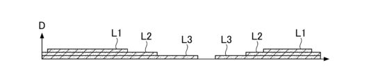
- FIG. 4 is a cross-sectional view showing an example of step S104.
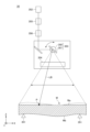
- FIG. 5 is a cross-sectional view showing an example of step S106.
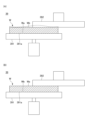
- FIG. 6A is a cross-sectional view showing an example of step S108
- FIG. 6B is a cross-sectional view showing an example of step S110.
- FIG. 7 is a plan view showing a substrate processing apparatus according to an embodiment.
- FIG. 8 is a functional block diagram showing an example of components of the control circuit.
- FIG. 8 is a functional block diagram showing an example of components of the control circuit.
- FIG. 9 is a plan view showing an example of movement of the irradiation point in the processing region.
- FIG. 10 is a cross-sectional view showing an example of a local recess.
- FIG. 11 is a plan view showing a modified example of the movement of the irradiation point in the processing region.
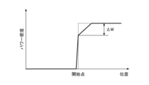
- FIG. 12 is a diagram showing an example of the power density at the irradiation point.
- FIG. 13(A) is a diagram showing an example of map data of the waviness of the first main surface obtained before laser processing
- FIG. 13(B) is a diagram showing an example of map data of the processing amount in laser processing
- FIG. 13(C) is a diagram showing an example of map data of the waviness of the first main surface obtained after grinding.
- a substrate processing method will be described with reference to Figures 1 to 6.
- the substrate processing method includes steps S101 to S110, as shown in Figure 1, for example. Steps S101 to S110 are performed under the control of a control circuit. Polishing may be performed instead of grinding.
- the substrate processing method does not have to include all steps S101 to S110 shown in FIG. 1. For example, since multiple substrates that make up the same lot are likely to have the same or similar waviness, steps S102 to S105 only need to be performed on one substrate.
- the processing conditions for one substrate may be used as the laser processing conditions for the remaining substrates. Multiple substrates (e.g., 25 substrates) that make up the same lot are cut simultaneously from a single crystal ingot and stored in the same cassette.
- the substrate processing method may further include a step not shown.
- An example of a step not shown is cleaning or etching of the substrate.
- the cleaning or etching of the substrate is performed, for example, immediately after the laser processing (step S106) or immediately after the grinding processing (step S108 or S110). Both cleaning and etching may be performed.
- the etching of the substrate may be performed before obtaining the waviness map data (step S102).
- the measurement accuracy of the waviness map data can be improved.
- the damage layer is no longer a problem, it is also possible to increase the cutting speed.
- Step S101 involves preparing a substrate W (see FIG. 2).
- Preparing the substrate W involves, for example, loading the substrate W into the substrate processing apparatus 1 described below.
- the substrate W is loaded into the substrate processing apparatus 1 while housed in a cassette C.
- the substrate W is a silicon wafer or a compound semiconductor wafer.
- the compound semiconductor wafer is not particularly limited, but may be, for example, a GaAs wafer, a SiC wafer, a GaN wafer, or an InP wafer.
- the substrate W is a bare wafer.
- the substrate W is, for example, disk-shaped.
- the substrate W may have a bevel on its periphery.
- the substrate W includes a first main surface Wa and a second main surface Wb facing in the opposite direction to the first main surface Wa.
- the substrate W has undulations on each of the first main surface Wa and the second main surface Wb.
- the undulations tend to have a shape that is linearly symmetrical about a reference line L0 extending in the cutting direction as shown in FIG. 13(A).
- the height of the map data is shown in grayscale. The closer the color is from black to white, the higher the height.
- the waviness of each of the first principal surface Wa and the second principal surface Wb is measured in advance by a waviness measuring device.
- the waviness measuring device may be of the contact type or the non-contact type.
- a commercially available three-dimensional measuring machine for example, SBW-330 manufactured by Kobelco Research Institute Co., Ltd., is used.
- the waviness is expressed as the height from a reference plane.
- the reference plane is a plane.
- the reference plane is, for example, a plane that approximates the central plane of the first principal surface Wa and the second principal surface Wb using the least squares method, but it may also be a crystal plane expressed by the desired Miller indices, or a plane inclined by the desired off angle from that crystal plane.
- Step S102 involves acquiring map data of undulations on the first principal surface Wa.
- Map data of undulations may be acquired for both the upper and lower surfaces of the substrate W, and a surface with a relatively small difference in undulation height may be set as the first principal surface Wa.
- the first principal surface Wa may be any surface that is to be laser processed.
- Step S103 involves creating map data of the processing amount D as shown in FIG. 3 based on the swell map data acquired in step S102.
- the dashed lines represent contour lines.
- the processing amount D is determined mainly by the height from a reference point P0 in the swell map data.
- the height of the reference point P0 is the height of the first main surface Wa obtained by laser processing.
- the reference point P0 may be the lowest point in the swell map data, or it may be a point shifted lower by a set amount from that lowest point.
- the map data for the processing amount D may be created using a model generated by machine learning.
- Step S104 involves dividing the map data of the processing amount D created in step S103 according to height as shown in FIG. 4 to create n layers L1, L2, and L3 (for example, three layers).
- n can be an integer equal to or greater than 2 and is not limited to 3.
- n is set based on the maximum value Dmax of the processing amount D and the processing amount per irradiation of the laser beam.
- the processing amount per irradiation is determined by the power density of the irradiation point P.
- n may also be set based on the upper limit of the surface roughness after laser processing.
- the n layers L1, L2, and L3 have the same thickness, but may have different thicknesses.
- the thickness of each of the n layers L1, L2, and L3 is set appropriately depending on the power density of the irradiation point P and the amount of overlap between the trajectories of adjacent irradiation points P, and is, for example, 0.1 ⁇ m to 1.0 ⁇ m.
- Step S105 involves setting a processing area for each of the layers L1, L2, and L3 created in step S104.
- the processing areas of the layers L1, L2, and L3 coincide with the layers L1, L2, and L3, respectively, but they do not have to coincide.
- the processing area of the layer L3, which is the bottom layer in FIG. 4 may be expanded so as to connect two separated layers L3.
- Step S106 includes performing laser processing of the first main surface Wa as shown in FIG. 5.
- the laser processing is an ablation process.
- the substrate W locally changes state from a solid phase to a gas phase and scatters, or scatters in the solid phase, and the substrate W is locally ablated. Details of the laser processing device 35 will be described later.
- Step S106 involves moving the irradiation point P of the laser beam LB in the processing area, for example for each of the layers L1, L2, and L3.
- the n layers L1, L2, and L3 are removed in a desired order. For example, a taller layer (e.g., layer L1) is removed before a shorter layer (e.g., layer L2).
- Step S106 involves moving the irradiation point P over the entire processing area of the kth layer to be removed, and then moving the irradiation point P over the entire processing area of the (k+1)th layer to be removed.
- k is an integer between 1 and (n-1). This removes layers L1, L2, and L3 for each layer L1, L2, and L3.
- the irradiation point P is moved in the processing area for each of the layers L1, L2, and L3.
- the n layers L1, L2, and L3 can be removed in the desired order. Since each of the layers L1, L2, and L3 has a constant thickness, it is not necessary to change the power density of the irradiation point P in most of the processing area, and it is not necessary to change the output of the light source. This simplifies the control of the laser processing.
- the n layers L1, L2, and L3 may have the same thickness as described above. There is no need to change the power density of the irradiation point P for each layer L1, L2, and L3, and there is no need to change the output of the light source. This makes it easier to control the laser processing. However, taking into account the gradient of the waviness, etc., two or more of the n layers L1, L2, and L3 may have different thicknesses.
- the irradiation point P is moved in the processing area for each of the layers L1, L2, and L3, but the technology disclosed herein is not limited to this. If the power density of the irradiation point P is changed each time according to the position of the irradiation point P while referring to the height of the map data of the processing amount D, it is not necessary to divide the map data of the processing amount D into n layers.
- Step S107 includes inverting the substrate W.
- Step S107 includes inverting the substrate W upside down so that the first main surface Wa of the substrate W faces downward and the second main surface Wb of the substrate W faces upward.
- Step S108 includes grinding the second main surface Wb while the first main surface Wa, which has been flattened by laser processing, is held by the suction surface 391a of the chuck 391, as shown in FIG. 6(A).
- the processing tool 392 includes, for example, a grindstone.
- the second main surface Wb can be flattened by grinding the second main surface Wb parallel to the first main surface Wa, which has been flattened in advance. Note that polishing may be performed instead of grinding.
- the suction surface 391a of the chuck 391 suctions the first main surface Wa while the first main surface Wa has undulations, the first main surface Wa will be flattened to imitate the suction surface 391a.
- the second main surface Wb is ground parallel to the first main surface Wa and then the suction of the substrate W is released, not only will the first main surface Wa return to a undulating state, but the same undulations as the first main surface Wa will also occur in the second main surface Wb.
- the second main surface Wb can be flattened by grinding the second main surface Wb parallel to the first main surface Wa, which has been flattened in advance by laser processing. Also, compared to flattening both sides of the substrate W with a laser beam, undulations present on both sides of the substrate W can be removed in a short time. This is because the processing speed of laser processing is slower than that of grinding processing.
- Step S109 includes inverting the substrate W.
- Step S109 includes inverting the substrate W upside down so that the first main surface Wa of the substrate W faces upward and the second main surface Wb of the substrate W faces downward.
- Step S110 includes performing grinding of the first main surface Wa while the second main surface Wb, which has been flattened by grinding, is adsorbed by the suction surface 391a of the chuck 391, as shown in FIG. 6(B). This makes it possible to make the processing quality of the first main surface Wa and the second main surface Wb equivalent. Since the first main surface Wa has already been flattened by laser processing, the amount of grinding of the first main surface Wa may be less than the amount of grinding of the second main surface Wb. Note that polishing may be performed instead of grinding.
- the substrate processing apparatus 1 performs steps S101 to S107 shown in FIG. 1. Steps S108 to S110 are performed outside the substrate processing apparatus 1.
- the substrate processing apparatus 1 may be equipped with a grinding apparatus 39 shown in FIG. 6(A) and FIG. 6(B) and may perform steps S108 to S110.
- a polishing apparatus may also be provided instead of the grinding apparatus 39.
- the substrate processing apparatus 1 includes a loading/unloading station 2, a processing station 3, and a control circuit 9.
- the loading/unloading station 2 and the processing station 3 are arranged in this order from the negative side in the X-axis direction to the positive side in the X-axis direction.
- the loading/unloading station 2 comprises a mounting table 20, a second transport area 21, and a second transport device 22.
- a plurality of cassettes C are mounted on the mounting table 20.
- Each cassette C contains a plurality of substrates W.
- a plurality of substrates W cut from a single crystal ingot are contained in the same cassette C.
- the second transfer region 21 is adjacent to the mounting table 20 and the transition device 33 of the processing station 3.
- the second transfer device 22 transfers substrates between multiple devices adjacent to the second transfer region 21.
- the second transfer device 22 has a transfer arm that holds the substrate W and a drive unit that moves or rotates the transfer arm.
- the transfer arm is capable of moving horizontally (in both the X-axis and Y-axis directions) and vertically, and of rotating about the vertical axis. Multiple transfer arms may be provided.
- the processing station 3 includes a first transport area 31, a first transport device 32, a transition device 33, a waviness measuring device 34, a laser processing device 35, a cleaning device 36, an inversion device 37, and an alignment device 38. Note that the arrangement and number of devices constituting the processing station 3 are not limited to those shown in FIG. 7.
- the first transfer region 31 is adjacent to a transition device 33, a waviness measuring device 34, a laser processing device 35, a cleaning device 36, an inversion device 37, and an alignment device 38.
- the first transfer device 32 transfers substrates between multiple devices adjacent to the first transfer region 31.
- the first transfer device 32 has a transfer arm that holds the substrate W, and a drive unit that moves or rotates the transfer arm.
- the transfer arm is capable of moving horizontally (in both the X-axis and Y-axis directions) and vertically, and of rotating about the vertical axis. Multiple transfer arms may be provided.
- the transition device 33 relays the substrate W between the second transport device 22 of the loading/unloading station 2 and the first transport device 32 of the processing station 3.
- the transition device 33 for relaying from the second transport device 22 to the first transport device 32 and the transition device 33 for relaying from the first transport device 32 to the second transport device 22 may be provided separately.
- the swell measuring device 34 measures the swell of the first main surface Wa of the substrate W.
- the swell measuring device 34 may also measure the swell of the second main surface Wb of the substrate W.
- the swell measuring device 34 transmits the measurement data to the control circuit 9.
- the control circuit 9 obtains map data of the swell of the first main surface Wa from the swell measuring device 34. Note that although the swell measuring device 34 is provided inside the substrate processing apparatus 1 in this embodiment, it may also be provided outside the substrate processing apparatus 1.
- the waviness measuring device 34 measures the waviness of the first main surface Wa of the substrate W before laser processing, but it may also measure the waviness of the first main surface Wa of the substrate W after laser processing. Also, the waviness measuring device 34 may measure the waviness of the first main surface Wa of the substrate W after grinding or polishing.
- the laser processing device 35 performs laser processing of the first main surface Wa of the substrate W.
- the laser processing device 35 moves the irradiation point P in the processing area for each of the layers L1, L2, L3, for example.
- the n layers L1, L2, L3 can be removed in the desired order.
- the inversion device 37 inverts the substrate W upside down. Like the transition device 33, the inversion device 37 may relay the substrate W between the first transport device 32 and the second transport device 22. The inversion device 37 and the transition device 33 may be stacked in the vertical direction.
- the alignment device 38 detects the notch of the substrate W while rotating the substrate W, thereby orienting the notch of the substrate W in the desired direction.
- the notch indicates the crystal orientation of the substrate W.
- the alignment device 38 may detect an orientation flat instead of the notch.
- the control circuit 9 is, for example, a computer, and includes an arithmetic unit 91 such as a CPU (Central Processing Unit), and a storage unit 92 such as a memory.
- the storage unit 92 stores programs that control various processes executed in the substrate processing apparatus 1.
- the control circuit 9 controls the operation of the substrate processing apparatus 1 by having the arithmetic unit 91 execute the programs stored in the storage unit 92.
- a lower control circuit that controls the operation of each device constituting the substrate processing apparatus 1 may be provided, and a higher-level control circuit that provides overall control of multiple lower-level control circuits may be provided.
- the control circuit 9 may be composed of the lower-level control circuit and the higher-level control circuit.
- the control circuit 9 includes electronic circuits such as a CPU, FPGA (Field Programmable Gate Array) or ASIC (Application Specific Integrated Circuit), and executes the various control operations described in this specification by executing instruction codes stored in memory or by being a circuit designed for a specific purpose.
- electronic circuits such as a CPU, FPGA (Field Programmable Gate Array) or ASIC (Application Specific Integrated Circuit)
- the control circuit 9 has, for example, a data acquisition unit 901, a processing amount setting unit 902, a layer creation unit 903, a processing area setting unit 904, a movement control unit 905, a power density control unit 906, and a model generation unit 907.
- the data acquisition unit 901 acquires map data of the waviness of the first main surface Wa of the substrate W.
- the processing amount setting unit 902 creates map data of the processing amount D in laser processing based on the waviness map data acquired by the data acquisition unit 901.
- the layer creation unit 903 creates n layers L1, L2, and L3 by dividing the map data of the processing amount D created by the processing amount setting unit 902 according to height.
- the processing area setting unit 904 sets a processing area for each of the layers L1, L2, and L3 created by the layer creation unit 903.
- the movement control unit 905 controls the movement of the irradiation point P in the processing area for each of the layers L1, L2, and L3.
- the power density control unit 906 controls the power density (unit: W/cm 2 ) at the irradiation point P.
- the model generation unit 907 generates a model used to create map data of the processing amount D, which will be described in detail later.
- each functional block shown in FIG. 8 is conceptual, and does not necessarily have to be physically configured as shown. It is possible to configure all or part of each functional block by distributing or integrating it functionally or physically in any unit. All or any part of each processing function performed by each functional block can be realized by a program executed by a CPU, or can be realized as hardware using wired logic.
- a transport device (not shown) transports the substrate W into the substrate processing apparatus 1. This allows the substrate W to be prepared (step S101).
- the substrate W is placed on the mounting table 20 while contained in a cassette C.
- the second transport device 22 removes the substrate W from the cassette C on the mounting table 20 and transports it to the transition device 33.
- the first transport device 32 of the processing station 3 removes the substrate W from the transition device 33 and transports it to the alignment device 38.
- the alignment device 38 detects the notch of the substrate W while rotating the substrate W, thereby orienting the notch of the substrate W in the desired direction.
- the first transport device 32 removes the substrate W from the alignment device 38 and transports it to the waviness measurement device 34.
- the waviness measuring device 34 measures the waviness of the first main surface Wa of the substrate W.
- the waviness measuring device 34 transmits the measurement data to the control circuit 9.
- the data acquisition unit 901 acquires map data of the waviness of the first main surface Wa (step S102).
- the processing amount setting unit 902 creates map data of the processing amount D in laser processing based on the waviness map data (step S103).
- the layer creation unit 903 creates n layers L1, L2, L3 by dividing the map data of the processing amount D according to height (step S104).
- the processing area setting unit 904 sets a processing area for each of the layers L1, L2, L3 (step S105).
- the first transport device 32 removes the substrate W from the waviness measuring device 34 and transports it to the laser processing device 35.
- steps S102 to S105 only need to be performed before the start of laser processing of the first main surface Wa (step S106). Steps S102 to S105 may also be performed after the first transport device 32 removes the substrate W from the waviness measuring device 34.
- the laser processing device 35 laser processes the first main surface Wa (step S106).
- the movement control unit 905 controls the movement of the irradiation point P in the processing area for each of the layers L1, L2, and L3.
- the first transport device 32 removes the substrate W from the laser processing device 35 and transports it to the cleaning device 36.
- the cleaning device 36 cleans the first main surface Wa of the substrate W.
- the first transport device 32 removes the substrate W from the cleaning device 36 and transports it to the inversion device 37.
- the inversion device 37 inverts the substrate W upside down (step S107).
- the second transport device 22 removes the substrate W from the inversion device 37 and stores it in a cassette C on the mounting table 20.
- a transport device (not shown) removes the substrate W stored in the cassette C from the substrate processing apparatus 1.
- the laser processing device 35 includes a substrate holder 351, a light source 352, and a galvanometer scanner 353.
- the laser processing device 35 may also include an f ⁇ lens 354, a homogenizer 355, and an aperture 356.
- the substrate holding part 351 holds the substrate W.
- the substrate holding part 351 holds the substrate W horizontally from below with the first main surface Wa of the substrate W facing upward.
- the substrate holding part 351 holds the substrate W in a natural state without adsorbing it and without any external forces acting other than gravity and its resistance.
- the substrate holding part 351 may also adsorb the substrate W.
- the substrate holding part 351 may be a vacuum chuck or an electrostatic chuck.
- the light source 352 emits a laser beam LB.
- the laser beam LB is, for example, UV light.
- the substrate W locally changes state from solid to gaseous and scatters, or scatters while remaining in the solid phase, and the substrate W is locally abraded.
- the laser beam LB may be focused and irradiated onto the upper surface of the substrate W.
- the irradiation point P is the focal point where the power density is highest, but it does not have to be a focal point.
- the light source 352 is, for example, a pulsed laser.
- the irradiation time per pulse is, for example, 30 nsec or less. If the irradiation time per pulse is 30 nsec or less, a laser beam LB with a high power density can be irradiated onto the substrate W in a short period of time, and overheating of the substrate W can be suppressed. This makes it possible to suppress deterioration of the substrate W due to heat, for example, to suppress the occurrence of a discolored layer.
- the irradiation time per pulse is preferably 10 psec or less. If the irradiation time per pulse is 10 psec or less, deterioration of the substrate W due to heat can be suppressed even if irradiation points P are formed multiple times at the same location.
- the galvanometer scanner 353 is disposed, for example, above the substrate W held by the substrate holder 351.
- the galvanometer scanner 353 allows the irradiation point P of the laser beam LB to be moved on the upper surface of the substrate W without moving the substrate holder 351. Even when the substrate holder 351 does not adsorb the substrate W, as long as the substrate holder 351 does not move, there is no misalignment of the substrate W relative to the substrate holder 351. Therefore, the position of the irradiation point P can be controlled with high precision.
- the galvanometer scanner 353 includes two pairs of galvanometer mirrors 357 and galvanometer motors 358 (only one pair is shown in FIG. 5).
- One galvanometer motor 358 rotates one galvanometer mirror 357, displacing the irradiation point P in the X-axis direction.
- Another galvanometer motor 358 rotates another galvanometer mirror 357, displacing the irradiation point P in the Y-axis direction.
- the galvano scanner 353 is an example of a moving unit that moves the irradiation point P.
- the moving unit may move the substrate holding unit 351 in the X-axis and Y-axis directions, and may have a motor and a ball screw mechanism that converts the rotational motion of the motor into linear motion of the substrate holding unit 351.
- the moving unit may also have a mechanism that rotates the substrate holding unit 351 around a vertical axis.
- the f ⁇ lens 354 forms a focal plane perpendicular to the Z-axis direction. While the galvanometer scanner 353 moves the position of the irradiation point P in the X-axis direction or the Y-axis direction, the f ⁇ lens 354 maintains the shape and dimensions of the irradiation point P on the upper surface of the substrate W. In this embodiment, the height of the irradiation point P matches the height of the focal plane, but it does not have to match the height of the focal plane, and may be higher or lower than the height of the focal plane.
- the homogenizer 355 converts the power density distribution of the laser beam LB from a Gaussian distribution to a top-hat distribution, homogenizing the power density.
- the aperture 356 shapes the cross-sectional shape of the laser beam LB into a rectangle.
- the aperture 356 is a light-shielding film with a rectangular opening. The opening allows the portion of the laser beam LB where the power density is constant to pass through.
- the homogenizer 355 and the aperture 356 can form a rectangular irradiation point P with uniform power density.
- the arrows indicate the movement direction and movement range of the irradiation point P.
- the movement range is the range from the start point of the movement to the end point of the movement.
- the arrows have the same meaning in FIG. 11 described later.
- the movement of the irradiation point P is not limited to the examples shown in FIG. 9 and FIG. 11.
- the movement of the irradiation point P may be performed in a spiral shape.
- the movement control unit 905 repeatedly controls the movement of the irradiation point P in a first direction (e.g., the positive direction of the X-axis) and the movement of the irradiation point P in a second direction (e.g., the negative direction of the X-axis) that is opposite to the first direction.
- the movement control unit 905 controls the shifting of the position of the irradiation point P in a third direction (e.g., the negative direction of the Y-axis) perpendicular to the first and second directions before and after changing the movement direction of the irradiation point P between the first and second directions.
- a first locus moving in the first direction of the irradiation point P and a second locus moving in the second direction of the irradiation point P, which are adjacent in the third direction, may partially overlap in the third direction.
- the pitch of the irradiation point P in the third direction may be smaller than the size of the irradiation point P in the third direction so that the first locus and the second locus partially overlap in the third direction.
- the movement control unit 905 may perform control to change the movement direction of the irradiation point P to vertical or diagonal between the kth layer to be removed and the (k+1)th layer to be removed.
- the movement control unit 905 may perform control to change the movement direction of the irradiation point P to vertical or diagonal between the odd-numbered layer to be removed and the even-numbered layer to be removed.
- the movement control unit 905 when removing odd-numbered layers L1 and L3, the movement control unit 905 repeatedly controls the movement of the irradiation point P in a first direction and the movement of the irradiation point P in a second direction. In addition, when removing odd-numbered layers L1 and L3, the movement control unit 905 controls the shifting of the position of the irradiation point P in a third direction before and after changing the movement direction of the irradiation point P between the first direction and the second direction.
- the movement control unit 905 when removing an even-numbered layer L2, the movement control unit 905 repeatedly controls the movement of the irradiation point P in the third direction and the movement of the irradiation point P in a fourth direction (e.g., the positive Y-axis direction) that is opposite to the third direction. Also, when removing an even-numbered layer L2, the movement control unit 905 controls the shifting of the position of the irradiation point P in the first direction or the second direction before and after changing the movement direction of the irradiation point P between the third direction and the fourth direction.
- a fourth direction e.g., the positive Y-axis direction
- the movement control unit 905 controls the movement direction of the irradiation point to change to vertical or diagonal (vertical in this embodiment) between the kth layer to be removed and the (k+1)th layer to be removed. This makes it possible to thin the processing marks formed along the movement direction of the irradiation point P. This makes it possible to reduce the surface roughness of the first main surface Wa after laser processing.
- a processing area A is set for each layer L1, L2, and L3.
- the periphery of the processing area A coincides with the periphery of each layer L1, L2, and L3.
- the start point where the movement of the irradiation point P begins and the end point where the movement of the irradiation point P ends are set on the periphery of the processing area A, for example, as shown in FIG. 9.
- the second main surface Wb is ground parallel to the first main surface Wa while the recesses Wc are formed on the first main surface Wa, and then the suction of the substrate W is released, a localized recess will be formed on the second main surface Wb, just like on the first main surface Wa.
- the movement control unit 905 controls the position of at least one of the start point and end point (both in FIG. 11) to be shifted from the periphery of the processing area A.
- the shift direction may be toward the inside of the processing area A, or toward the outside of the processing area A.
- the shift distance ⁇ L is set in advance through experiments, etc.
- the movement control unit 905 shifts the positions of both the start point and the end point from the periphery of the processing area A both when moving the irradiation point P in the first direction and when moving the irradiation point P in the second direction, but the technology disclosed herein is not limited to this.
- the start point and the end point may be positioned in a zigzag pattern along the periphery of the processing area A, that is, so as to repeatedly move toward and away from the periphery along the periphery of the processing area A.
- the movement control unit 905 shifts the positions of both the start point and the end point from the periphery of the processing area A when moving the irradiation point P in a first direction, it is not necessary for the movement control unit 905 to shift the start point and the irradiation point from the periphery of the processing area A when moving the irradiation point P in a second direction.
- the movement control unit 905 may shift the position of only the start point from the periphery of the processing area A or shift the position of only the end point from the periphery of the processing area A both when moving the irradiation point P in the first direction and when moving the irradiation point P in the second direction.
- the start point and end point can be arranged in a zigzag pattern along the periphery of the processing area A, that is, so as to repeatedly approach and move away from the periphery along the periphery of the processing area A. This can suppress the formation of recesses Wc. This effect is noticeable when the first and second trajectories adjacent to each other in the third direction partially overlap in the third direction.
- first locus and a second locus that are adjacent in the third direction overlap partially in the third direction
- start point of the first locus and the end point of the second locus are positioned apart so as not to overlap with each other.
- end point of the first locus and the start point of the second locus are positioned apart so as not to overlap with each other. This makes it possible to suppress the formation of recesses Wc.
- the power density control unit 906 may perform control to reduce the power density of the irradiation point P on the periphery of the processing area A compared to the center of the processing area A.
- the amount of reduction in power density ⁇ W is set in advance through experiments, etc.
- the power density of the irradiation point P is controlled, for example, by the output of the light source 352.
- the control shown in FIG. 11 and the control shown in FIG. 12 may be used in combination.
- the control shown in FIG. 11 and the control shown in FIG. 12 may also be applied when the map data of the processing amount D is not divided into n layers L1, L2, and L3. In this case as well, it is possible to prevent the recesses Wc from being formed locally along the periphery of the processing area A, thereby improving the processing quality of the laser processing.
- Figure 13(A) is map data of the waviness of the first principal surface Wa obtained before laser processing.
- Figure 13(B) is map data of the processing amount D in laser processing.
- Figure 13(C) is map data of the waviness of the first principal surface Wa obtained after grinding.
- the height of the map data is shown in grayscale. The closer the color is from black to white, the higher the height.
- the inventors of the present application created map data of the processing amount D so that the waviness of the first main surface Wa would be completely eliminated by laser processing, and performed laser processing of the first main surface Wa according to the map data. They discovered that in some cases, the waviness of the first main surface Wa was not completely eliminated and remained after the grinding process. It is believed that unintended deformation of the substrate W occurs during the laser processing or grinding process. As mentioned above, polishing may be performed instead of grinding.
- the processing amount setting unit 902 may create map data for the processing amount D in the current laser processing based on the desired data of a substrate W on which laser processing of the first main surface Wa, grinding or polishing of the second main surface Wb, and grinding or polishing of the first main surface Wa have been previously performed in that order, in addition to the map data of the waviness of the first main surface Wa obtained before the current laser processing.
- the desired data includes, for example, (A) map data of the waviness of the first main surface Wa obtained before laser processing, (B) map data of the processing amount D in the laser processing, and (C) data of the waviness of the first main surface Wa obtained after grinding or polishing.
- the data on the waviness of the first main surface Wa obtained after grinding or polishing is map data, but it may simply be data on the height difference.
- the height difference of the waviness after grinding or polishing is used as scoring data for the map data of the processing amount. The smaller the height difference of the waviness after grinding or polishing, the better the score.
- the map data of the processing amount D in the current laser processing can be appropriately corrected.
- the height difference of the waviness of the first main surface Wa obtained after the current grinding or polishing processing can be reduced.
- a regression analysis or the like can be performed to absorb errors resulting from unintended deformations thought to have occurred in previous laser processing, grinding, or polishing processes, and the map data for the processing amount D in the current laser processing can be corrected. By feeding back past data into the current processing conditions, the flatness of the substrate W can be improved.
- the processing amount setting unit 902 may input map data of the waviness of the first main surface Wa obtained before the current laser processing into a model that has been machine-learned using the desired data as training data, and output map data of the processing amount D in the current laser processing so that the height difference of the waviness after the current grinding or polishing process is equal to or less than a set value.
- the map data of the processing amount D can be appropriately corrected regardless of the user's level of skill, that is, without relying on the user's experience and intuition.
- the data input to the machine-learned model may include (D) map data of the waviness of the first main surface Wa obtained before the current laser processing, as well as (E) map data of the waviness of the first main surface Wa to be obtained after the current grinding or polishing processing.
- the data input to the model may include (F) the height difference of the waviness of the first main surface Wa to be obtained after the current grinding or polishing processing, instead of (E).
- the model may be read from a storage unit in advance and used, or may be generated by the model generation unit 907.
- the model generation unit 907 uses the desired data as teacher data and generates the model through supervised learning using a known machine learning algorithm such as a convolutional neural network (CNN).
- CNN convolutional neural network
- the processing amount setting unit 902 is an example of a processing condition setting unit.
- the processing condition setting unit sets the current laser processing conditions based on desired data acquired in the past, in addition to map data of the waviness of the first main surface Wa acquired before the current laser processing.
- the laser processing conditions may include, for example, at least one selected from map data of the processing amount D, the number of layers L1, L2, and L3, the thicknesses of each of the layers L1, L2, and L3, ⁇ L shown in FIG. 11, and ⁇ W shown in FIG. 12.
Landscapes
- Physics & Mathematics (AREA)
- Optics & Photonics (AREA)
- Engineering & Computer Science (AREA)
- Plasma & Fusion (AREA)
- Mechanical Engineering (AREA)
- Laser Beam Processing (AREA)
Priority Applications (3)
| Application Number | Priority Date | Filing Date | Title |
|---|---|---|---|
| JP2025512532A JPWO2024210048A1 (https=) | 2023-04-07 | 2024-03-29 | |
| KR1020257037012A KR20250174051A (ko) | 2023-04-07 | 2024-03-29 | 기판 처리 방법 및 기판 처리 장치 |
| CN202480021449.8A CN120981892A (zh) | 2023-04-07 | 2024-03-29 | 基板处理方法和基板处理装置 |
Applications Claiming Priority (2)
| Application Number | Priority Date | Filing Date | Title |
|---|---|---|---|
| JP2023-062771 | 2023-04-07 | ||
| JP2023062771 | 2023-04-07 |
Publications (1)
| Publication Number | Publication Date |
|---|---|
| WO2024210048A1 true WO2024210048A1 (ja) | 2024-10-10 |
Family
ID=92971712
Family Applications (1)
| Application Number | Title | Priority Date | Filing Date |
|---|---|---|---|
| PCT/JP2024/012955 Ceased WO2024210048A1 (ja) | 2023-04-07 | 2024-03-29 | 基板処理方法および基板処理装置 |
Country Status (5)
| Country | Link |
|---|---|
| JP (1) | JPWO2024210048A1 (https=) |
| KR (1) | KR20250174051A (https=) |
| CN (1) | CN120981892A (https=) |
| TW (1) | TW202442353A (https=) |
| WO (1) | WO2024210048A1 (https=) |
Citations (8)
| Publication number | Priority date | Publication date | Assignee | Title |
|---|---|---|---|---|
| US4986664A (en) * | 1984-02-07 | 1991-01-22 | International Technical Associates | System and process for controlled removal of material to produce a desired surface contour |
| US5953578A (en) * | 1998-09-08 | 1999-09-14 | Winbond Electronics Corp. | Global planarization method using plasma etching |
| JP2018065147A (ja) * | 2016-10-17 | 2018-04-26 | 矢崎総業株式会社 | レーザ加工方法及びレーザ加工装置 |
| WO2020202976A1 (ja) * | 2019-04-05 | 2020-10-08 | 東京エレクトロン株式会社 | レーザー加工装置、基板処理システム、レーザー加工方法、および基板処理方法 |
| WO2022054611A1 (ja) * | 2020-09-09 | 2022-03-17 | 東京エレクトロン株式会社 | レーザー加工装置、及びレーザー加工方法 |
| WO2022158333A1 (ja) * | 2021-01-21 | 2022-07-28 | 東京エレクトロン株式会社 | 基板加工方法、及び基板加工装置 |
| JP2022148013A (ja) * | 2021-03-24 | 2022-10-06 | 株式会社東京精密 | シリコンウエハの表面改質方法 |
| JP2023104449A (ja) * | 2022-01-18 | 2023-07-28 | 株式会社東京精密 | 半導体ウエハ表面の平坦化装置 |
Family Cites Families (1)
| Publication number | Priority date | Publication date | Assignee | Title |
|---|---|---|---|---|
| JP3943869B2 (ja) | 2000-06-29 | 2007-07-11 | 信越半導体株式会社 | 半導体ウエーハの加工方法および半導体ウエーハ |
-
2024
- 2024-03-28 TW TW113111572A patent/TW202442353A/zh unknown
- 2024-03-29 JP JP2025512532A patent/JPWO2024210048A1/ja active Pending
- 2024-03-29 CN CN202480021449.8A patent/CN120981892A/zh active Pending
- 2024-03-29 KR KR1020257037012A patent/KR20250174051A/ko active Pending
- 2024-03-29 WO PCT/JP2024/012955 patent/WO2024210048A1/ja not_active Ceased
Patent Citations (8)
| Publication number | Priority date | Publication date | Assignee | Title |
|---|---|---|---|---|
| US4986664A (en) * | 1984-02-07 | 1991-01-22 | International Technical Associates | System and process for controlled removal of material to produce a desired surface contour |
| US5953578A (en) * | 1998-09-08 | 1999-09-14 | Winbond Electronics Corp. | Global planarization method using plasma etching |
| JP2018065147A (ja) * | 2016-10-17 | 2018-04-26 | 矢崎総業株式会社 | レーザ加工方法及びレーザ加工装置 |
| WO2020202976A1 (ja) * | 2019-04-05 | 2020-10-08 | 東京エレクトロン株式会社 | レーザー加工装置、基板処理システム、レーザー加工方法、および基板処理方法 |
| WO2022054611A1 (ja) * | 2020-09-09 | 2022-03-17 | 東京エレクトロン株式会社 | レーザー加工装置、及びレーザー加工方法 |
| WO2022158333A1 (ja) * | 2021-01-21 | 2022-07-28 | 東京エレクトロン株式会社 | 基板加工方法、及び基板加工装置 |
| JP2022148013A (ja) * | 2021-03-24 | 2022-10-06 | 株式会社東京精密 | シリコンウエハの表面改質方法 |
| JP2023104449A (ja) * | 2022-01-18 | 2023-07-28 | 株式会社東京精密 | 半導体ウエハ表面の平坦化装置 |
Also Published As
| Publication number | Publication date |
|---|---|
| JPWO2024210048A1 (https=) | 2024-10-10 |
| TW202442353A (zh) | 2024-11-01 |
| CN120981892A (zh) | 2025-11-18 |
| KR20250174051A (ko) | 2025-12-11 |
Similar Documents
| Publication | Publication Date | Title |
|---|---|---|
| JP7483020B2 (ja) | レーザー加工装置、及びレーザー加工方法 | |
| JP7655651B2 (ja) | 基板加工方法、及び基板加工装置 | |
| US11090766B2 (en) | Laser processing apparatus | |
| US9649775B2 (en) | Workpiece dividing method | |
| JP7118245B2 (ja) | 基板処理システム、および基板処理方法 | |
| US20130014905A1 (en) | Film peeling apparatus and film peeling method | |
| WO2024210026A1 (ja) | 基板処理方法および基板処理装置 | |
| JP6012185B2 (ja) | 半導体デバイスの製造方法 | |
| WO2024210048A1 (ja) | 基板処理方法および基板処理装置 | |
| WO2024209992A1 (ja) | 基板処理方法および基板処理装置 | |
| JP2005118832A (ja) | レーザー加工方法およびレーザー加工装置 | |
| JP5969214B2 (ja) | 半導体デバイスの製造方法 | |
| JP5442801B2 (ja) | 半導体切断装置および半導体切断方法 | |
| WO2025258398A1 (ja) | 基板処理方法および基板処理装置 | |
| WO2019239801A1 (ja) | 基板処理システム、および基板処理方法 | |
| JP2007329357A (ja) | 半導体装置切断システムおよび半導体装置切断方法 | |
| WO2025047207A1 (ja) | 基板処理方法および基板処理システム | |
| TW202604664A (zh) | 雷射加工裝置及雷射加工方法 | |
| JP7802178B2 (ja) | 基板処理方法、および基板処理装置 | |
| JP2013157449A (ja) | 半導体デバイスの製造方法 | |
| JP2023032215A (ja) | 加工方法 |
Legal Events
| Date | Code | Title | Description |
|---|---|---|---|
| 121 | Ep: the epo has been informed by wipo that ep was designated in this application |
Ref document number: 24784834 Country of ref document: EP Kind code of ref document: A1 |
|
| ENP | Entry into the national phase |
Ref document number: 2025512532 Country of ref document: JP Kind code of ref document: A |
|
| WWE | Wipo information: entry into national phase |
Ref document number: 2025512532 Country of ref document: JP Ref document number: CN2024800214498 Country of ref document: CN |
|
| ENP | Entry into the national phase |
Ref document number: 1020257037012 Country of ref document: KR Free format text: ST27 STATUS EVENT CODE: A-0-1-A10-A15-NAP-PA0105 (AS PROVIDED BY THE NATIONAL OFFICE) |
|
| WWE | Wipo information: entry into national phase |
Ref document number: KR1020257037012 Country of ref document: KR |
|
| NENP | Non-entry into the national phase |
Ref country code: DE |
|
| 122 | Ep: pct application non-entry in european phase |
Ref document number: 24784834 Country of ref document: EP Kind code of ref document: A1 |