WO2024203971A1 - 二次元層状物質および多孔質膜を含む積層体、積層体の転写方法、および、積層体の製造方法 - Google Patents
二次元層状物質および多孔質膜を含む積層体、積層体の転写方法、および、積層体の製造方法 Download PDFInfo
- Publication number
- WO2024203971A1 WO2024203971A1 PCT/JP2024/011525 JP2024011525W WO2024203971A1 WO 2024203971 A1 WO2024203971 A1 WO 2024203971A1 JP 2024011525 W JP2024011525 W JP 2024011525W WO 2024203971 A1 WO2024203971 A1 WO 2024203971A1
- Authority
- WO
- WIPO (PCT)
- Prior art keywords
- laminate
- graphene
- film
- porous
- membrane
- Prior art date
- Legal status (The legal status is an assumption and is not a legal conclusion. Google has not performed a legal analysis and makes no representation as to the accuracy of the status listed.)
- Ceased
Links
Images










Classifications
-
- G—PHYSICS
- G01—MEASURING; TESTING
- G01N—INVESTIGATING OR ANALYSING MATERIALS BY DETERMINING THEIR CHEMICAL OR PHYSICAL PROPERTIES
- G01N33/00—Investigating or analysing materials by specific methods not covered by groups G01N1/00 - G01N31/00
- G01N33/48—Biological material, e.g. blood, urine; Haemocytometers
- G01N33/50—Chemical analysis of biological material, e.g. blood, urine; Testing involving biospecific ligand binding methods; Immunological testing
- G01N33/53—Immunoassay; Biospecific binding assay; Materials therefor
- G01N33/543—Immunoassay; Biospecific binding assay; Materials therefor with an insoluble carrier for immobilising immunochemicals
- G01N33/54366—Apparatus specially adapted for solid-phase testing
- G01N33/54373—Apparatus specially adapted for solid-phase testing involving physiochemical end-point determination, e.g. wave-guides, FETS, gratings
- G01N33/5438—Electrodes
-
- C—CHEMISTRY; METALLURGY
- C01—INORGANIC CHEMISTRY
- C01B—NON-METALLIC ELEMENTS; COMPOUNDS THEREOF; METALLOIDS OR COMPOUNDS THEREOF NOT COVERED BY SUBCLASS C01C
- C01B32/00—Carbon; Compounds thereof
- C01B32/15—Nano-sized carbon materials
- C01B32/182—Graphene
- C01B32/184—Preparation
- C01B32/186—Preparation by chemical vapour deposition [CVD]
-
- B—PERFORMING OPERATIONS; TRANSPORTING
- B32—LAYERED PRODUCTS
- B32B—LAYERED PRODUCTS, i.e. PRODUCTS BUILT-UP OF STRATA OF FLAT OR NON-FLAT, e.g. CELLULAR OR HONEYCOMB, FORM
- B32B27/00—Layered products comprising a layer of synthetic resin
-
- B—PERFORMING OPERATIONS; TRANSPORTING
- B32—LAYERED PRODUCTS
- B32B—LAYERED PRODUCTS, i.e. PRODUCTS BUILT-UP OF STRATA OF FLAT OR NON-FLAT, e.g. CELLULAR OR HONEYCOMB, FORM
- B32B3/00—Layered products comprising a layer with external or internal discontinuities or unevennesses, or a layer of non-planar shape; Layered products comprising a layer having particular features of form
- B32B3/26—Layered products comprising a layer with external or internal discontinuities or unevennesses, or a layer of non-planar shape; Layered products comprising a layer having particular features of form characterised by a particular shape of the outline of the cross-section of a continuous layer; characterised by a layer with cavities or internal voids ; characterised by an apertured layer
- B32B3/266—Layered products comprising a layer with external or internal discontinuities or unevennesses, or a layer of non-planar shape; Layered products comprising a layer having particular features of form characterised by a particular shape of the outline of the cross-section of a continuous layer; characterised by a layer with cavities or internal voids ; characterised by an apertured layer characterised by an apertured layer, the apertures going through the whole thickness of the layer, e.g. expanded metal, perforated layer, slit layer regular cells B32B3/12
-
- B—PERFORMING OPERATIONS; TRANSPORTING
- B32—LAYERED PRODUCTS
- B32B—LAYERED PRODUCTS, i.e. PRODUCTS BUILT-UP OF STRATA OF FLAT OR NON-FLAT, e.g. CELLULAR OR HONEYCOMB, FORM
- B32B5/00—Layered products characterised by the non- homogeneity or physical structure, i.e. comprising a fibrous, filamentary, particulate or foam layer; Layered products characterised by having a layer differing constitutionally or physically in different parts
- B32B5/18—Layered products characterised by the non- homogeneity or physical structure, i.e. comprising a fibrous, filamentary, particulate or foam layer; Layered products characterised by having a layer differing constitutionally or physically in different parts characterised by features of a layer of foamed material
-
- B—PERFORMING OPERATIONS; TRANSPORTING
- B32—LAYERED PRODUCTS
- B32B—LAYERED PRODUCTS, i.e. PRODUCTS BUILT-UP OF STRATA OF FLAT OR NON-FLAT, e.g. CELLULAR OR HONEYCOMB, FORM
- B32B9/00—Layered products comprising a layer of a particular substance not covered by groups B32B11/00 - B32B29/00
- B32B9/005—Layered products comprising a layer of a particular substance not covered by groups B32B11/00 - B32B29/00 comprising one layer of ceramic material, e.g. porcelain, ceramic tile
- B32B9/007—Layered products comprising a layer of a particular substance not covered by groups B32B11/00 - B32B29/00 comprising one layer of ceramic material, e.g. porcelain, ceramic tile comprising carbon, e.g. graphite, composite carbon
-
- B—PERFORMING OPERATIONS; TRANSPORTING
- B32—LAYERED PRODUCTS
- B32B—LAYERED PRODUCTS, i.e. PRODUCTS BUILT-UP OF STRATA OF FLAT OR NON-FLAT, e.g. CELLULAR OR HONEYCOMB, FORM
- B32B9/00—Layered products comprising a layer of a particular substance not covered by groups B32B11/00 - B32B29/00
- B32B9/04—Layered products comprising a layer of a particular substance not covered by groups B32B11/00 - B32B29/00 comprising such particular substance as the main or only constituent of a layer, which is next to another layer of the same or of a different material
- B32B9/045—Layered products comprising a layer of a particular substance not covered by groups B32B11/00 - B32B29/00 comprising such particular substance as the main or only constituent of a layer, which is next to another layer of the same or of a different material of synthetic resin
-
- C—CHEMISTRY; METALLURGY
- C23—COATING METALLIC MATERIAL; COATING MATERIAL WITH METALLIC MATERIAL; CHEMICAL SURFACE TREATMENT; DIFFUSION TREATMENT OF METALLIC MATERIAL; COATING BY VACUUM EVAPORATION, BY SPUTTERING, BY ION IMPLANTATION OR BY CHEMICAL VAPOUR DEPOSITION, IN GENERAL; INHIBITING CORROSION OF METALLIC MATERIAL OR INCRUSTATION IN GENERAL
- C23C—COATING METALLIC MATERIAL; COATING MATERIAL WITH METALLIC MATERIAL; SURFACE TREATMENT OF METALLIC MATERIAL BY DIFFUSION INTO THE SURFACE, BY CHEMICAL CONVERSION OR SUBSTITUTION; COATING BY VACUUM EVAPORATION, BY SPUTTERING, BY ION IMPLANTATION OR BY CHEMICAL VAPOUR DEPOSITION, IN GENERAL
- C23C16/00—Chemical coating by decomposition of gaseous compounds, without leaving reaction products of surface material in the coating, i.e. chemical vapour deposition [CVD] processes
- C23C16/22—Chemical coating by decomposition of gaseous compounds, without leaving reaction products of surface material in the coating, i.e. chemical vapour deposition [CVD] processes characterised by the deposition of inorganic material, other than metallic material
- C23C16/26—Deposition of carbon only
-
- G—PHYSICS
- G01—MEASURING; TESTING
- G01N—INVESTIGATING OR ANALYSING MATERIALS BY DETERMINING THEIR CHEMICAL OR PHYSICAL PROPERTIES
- G01N33/00—Investigating or analysing materials by specific methods not covered by groups G01N1/00 - G01N31/00
- G01N33/48—Biological material, e.g. blood, urine; Haemocytometers
- G01N33/50—Chemical analysis of biological material, e.g. blood, urine; Testing involving biospecific ligand binding methods; Immunological testing
- G01N33/53—Immunoassay; Biospecific binding assay; Materials therefor
- G01N33/531—Production of immunochemical test materials
- G01N33/532—Production of labelled immunochemicals
-
- B—PERFORMING OPERATIONS; TRANSPORTING
- B32—LAYERED PRODUCTS
- B32B—LAYERED PRODUCTS, i.e. PRODUCTS BUILT-UP OF STRATA OF FLAT OR NON-FLAT, e.g. CELLULAR OR HONEYCOMB, FORM
- B32B9/00—Layered products comprising a layer of a particular substance not covered by groups B32B11/00 - B32B29/00
Definitions
- the present invention relates to a laminate including a graphene film laminated with a porous film having micropores, a transfer method for the laminate, and a manufacturing method for the laminate.
- Graphene has excellent properties such as optical transparency and high electrical conductivity, and is expected to be applied to transparent conductive films.
- CVD chemical vapor deposition
- a carbon source gas such as methane is used as the raw material to form a film of graphene on a catalytic metal substrate such as copper.
- Graphene is a sheet material with a thickness of one atom and cannot stand on its own.
- polymethyl methacrylate PMMA
- a PMMA film is formed on graphene on a metal catalyst (copper) by spin-coating a PMMA solution, and then a laminate of PMMA, graphene, and copper is floated in a copper etching solution. At this time, the copper side is floated in the etching solution so that it is in contact with the etching solution, and the copper is etched. After all the copper is etched, the remaining PMMA/graphene laminate is transferred to a pool of pure water and floated there. If necessary, the graphene is washed by repeatedly transferring it to the pure water pool.
- the PMMA and graphene laminate floating on the pure water is then scooped up on the desired substrate.
- the PMMA present on the top surface of the laminate is dissolved and removed using a solvent such as acetone, completing the transfer of graphene onto the desired substrate. If an attempt is made to pull up the laminate consisting of PMMA and graphene floating on the water surface directly from the water surface using tweezers or the like, without scooping it up with the desired substrate, the stress inside the PMMA film and the surface tension of the water will act, causing the laminate to become wrinkled and damaging the graphene.
- the graphene using the PMMA film as the transfer support film after removing the copper substrate must be floated on the water surface before and during the transfer process to the desired substrate, and cannot stand on its own in the air.
- the presence of the process of floating on pure water in the transfer process was one of the main causes of the reduced mass productivity and reproducibility in graphene production.
- Non-Patent Document 1 reports a graphene transfer method using a commercially available laminator and a polyvinyl alcohol (PVA) film.
- PVA polyvinyl alcohol
- the graphene is transferred by stacking this graphene and PVA laminate on a desired substrate (SiO 2 /Si substrate in the literature) and passing through a laminator. Then, the PVA film is dissolved and removed with hot water.
- This method does not include a step of scooping the laminate floating on the water surface, but it is difficult to avoid damage to the graphene because the copper and graphene are mechanically peeled off.
- a method using electrochemical transfer and functional tape has been proposed.
- Non-Patent Document 2 a UV tape in which a UV-sensitive adhesive substance is coated on polyolefin is brought into contact with graphene on copper, and UV is irradiated to produce a laminate consisting of UV tape, graphene, and copper foil.
- a laminate that can be transferred without floating on water is produced by peeling the UV tape/graphene laminate from the copper foil by electrochemical transfer.
- This laminate is attached to a desired substrate and heated to 90° C., the tape is peeled off from the graphene, completing the transfer.
- This transfer method is a transfer method that does not involve dissolving the support material, and the process of peeling the UV tape, which is the support material, from the graphene film can be said to be a type of mechanical peeling method.
- the objective of the present invention is to provide a method for easily transferring high-quality two-dimensional layered materials such as graphene to a desired substrate without the need to float the material on the water surface and without causing damage during the transfer process, and to provide a laminate for use therein.
- the polymer is deformed by a heating process for welding, etc., and if deformation occurs at the point of contact with the graphene, it is one of the factors that damage the graphene.
- the tensile stress of the transfer support film exerts a compressive force on the substrate (graphene/copper foil) that binds the transfer support material. In other words, compressive stress is generated in the graphene/copper foil.
- the laminate consisting of the transfer support material and the graphene film is left in the atmosphere with nothing to restrain the deformation of the transfer support film other than the graphene, which is one atomic layer thick, so the graphene is subjected to a large compressive stress and is thought to easily wrinkle.
- the inventors attempted to produce a laminate consisting of a porous film and graphene.
- the laminate after etching the copper foil catalyst metal could stand on its own in the air while maintaining its planar structure, and the graphene in the laminate had extremely little breakage.
- the present invention has been completed based on the above findings and includes the following aspects:
- One aspect of the present invention is [1] A laminate comprising a two-dimensional layered material and a porous membrane laminated on the two-dimensional layered material,
- the present invention relates to a laminate that can stand on its own in the atmosphere while maintaining its planar structure.
- [2] The laminate according to [1] above It is characterized by being in a dry state.
- the porous membrane is characterized in that it has pores with an average pore size of 20 nm or more.
- the porous membrane is characterized in that the area ratio of the pores to the membrane surface is 20% or more.
- [5] The laminate according to any one of [1] to [4] above, The porous film has a thickness of 100 nm or more.
- porous membrane is a membrane made of a material selected from the group consisting of nitrocellulose, cellulose acetate, polyethersulfone, polytetrafluoroethylene, polyamide, polyvinylidene fluoride, regenerated cellulose, polycarbonate, polypropylene, polyvinylidene chloride, aluminum oxide, glass fiber, quartz fiber, polymethyl methacrylate, polystyrene, polyethylene, polyethylene terephthalate, and ceramic, or a mixed membrane made of two or more materials selected from the group.
- the porous membrane is characterized in that it is a membrane made of a material selected from the group consisting of nitrocellulose, cellulose acetate, polycarbonate, polyvinylidene chloride, polystyrene, and polymethyl methacrylate, or a mixed membrane made of two or more materials selected from the group.
- the present invention comprises: [8] A method for transferring the laminate according to any one of [1] to [7] above onto a desired substrate, comprising the steps of: (a) bonding the two-dimensional layered material side of the laminate to a desired position on the desired substrate.
- the present invention comprises: [10] A method for producing the laminate according to any one of [1] to [7] above, (i) forming a two-dimensional layered material on a metal catalyst substrate by a CVD method; (ii) forming a porous film on the two-dimensional layered material to produce a laminate; and (iii) removing the metal catalyst substrate by etching.
- the present invention relates to a method for producing a laminate.
- the method for producing a laminate of the present invention includes the steps of: [11] A method for producing the laminate according to [10] above, The method is characterized in that the formation of the porous film on the two-dimensional layered material in the step (ii) is carried out by a phase inversion method.
- the solvent for dissolving the polymer used to form the porous membrane is a mixed solvent containing a good solvent and a poor solvent for the polymer.
- the laminate of the present invention makes it possible to easily transfer high-quality two-dimensional layered materials to a desired substrate without the need to float it on a water surface and without causing damage during the transfer process. Furthermore, the laminate of the present invention can stand on its own in the air, making it easy to store and transport.
- FIG. 1 is a schematic diagram showing one embodiment of a laminate according to the present invention, which comprises a porous membrane and a two-dimensional layered material.
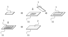
- Fig. 2A shows a scheme of one embodiment of the method for transferring a laminate according to the present invention.
- Fig. 2A shows a method for transferring a laminate 1 to a substrate 11 by covering a laminate (porous film/two-dimensional layered material) loaded on a membrane.
- 2B shows a scheme of one embodiment of the method for transferring a laminate according to the present invention.
- FIG 2B shows a method for transferring a laminate mounted on a membrane onto a substrate.
- FIG. 2C shows a scheme of one embodiment of the method for transferring a laminate according to the present invention, which illustrates a method for directly transferring a laminate onto a substrate without using a membrane.
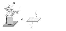
- FIG. 2D shows a schematic diagram of exposing the laminate to acetone vapor to dissolve and remove the porous film.
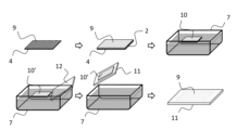
- FIG. 3A shows a scheme of one embodiment of a method for producing a laminate according to the present invention.
- FIG. 3B shows a fabrication scheme for a graphene electrode using a conventional PMMA as a transfer support film.
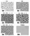
- FIG. 4 shows an SEM image of the porous membrane surface of the porous membrane/graphene laminate produced in Example 1 below.
- FIG. 5 shows a histogram of the pore sizes of pores present on the surface of the porous membrane of the porous membrane/graphene laminate produced in Example 1 below.
- FIG. 6 shows a histogram of the pore sizes of pores present on the surface of the porous membrane of the porous membrane/graphene laminate produced in Example 1 below.
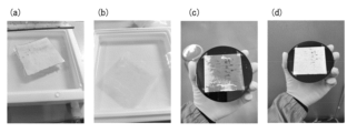
- Fig. 7(a) shows an image of a PMMA film/graphene film laminate scooped onto a membrane and dried, as performed in Example 3 below, while Fig. 7(b) shows an image of a cellulose mixed ester/graphene film laminate scooped onto a membrane and dried.
- Fig. 8 shows SEM images of the surface of the cellulose mixed ester membrane prepared in Example 5 below.
- FIG. 8(a) shows an SEM image of the surface of the cellulose mixed ester membrane prepared using an acetone solvent
- Fig. 8(b) shows an SEM image of the surface of the cellulose mixed ester membrane prepared using an acetone/formamide mixed solvent
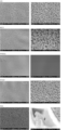
- Fig. 9 shows SEM images of the surfaces of the porous membranes of six types of porous membrane/graphene laminates prepared by a casting method in Example 5 below.
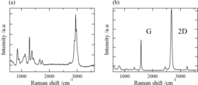
- Fig. 10(a) shows the Raman spectrum of the porous mixed cellulose ester film/graphene film/quartz substrate laminate prepared in Example 5 below.
- Fig. 10(b) shows the Raman spectrum of the graphene film on the quartz glass substrate from which the porous mixed cellulose ester film has been removed.
- FIG. 11 shows SEM images of the cellulose mixed ester film in the laminate consisting of the porous cellulose mixed ester film/graphene film/copper foil prepared in Example 6 below.
- Fig. 11(a) shows an SEM image of the laminate in which the gap height of the applicator during preparation of the cellulose mixed ester film is 25 ⁇ m.
- Figs. 11(b) to (d) show SEM images of the laminate in which the gap height of the applicator during preparation of the cellulose mixed ester film is 50 ⁇ m, 75 ⁇ m, and 100 ⁇ m, respectively.
- FIG. 12 shows an image of the mixed cellulose ester film prepared in Example 7 below, in which the applicator gap height was set to 300 ⁇ m.
- FIG. 11(a) shows an SEM image of the laminate in which the gap height of the applicator during preparation of the cellulose mixed ester film is 25 ⁇ m.
- Figs. 11(b) to (d) show SEM images of the laminate in which the gap height
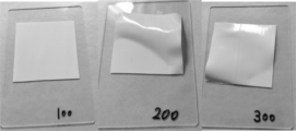
- FIG. 13 shows an image of the mixed cellulose ester film (prepared with an applicator gap height of 100 ⁇ m, 200 ⁇ m, or 300 ⁇ m) prepared in Example 7 below, transferred onto a slide glass.
- FIG. 14 shows images of cellulose mixed ester films (prepared with applicator gap heights of 100 ⁇ m, 200 ⁇ m, or 300 ⁇ m) formed on graphene grown on copper foil as prepared in Example 7 below.
- FIG. 15 shows an image of a laminate produced in Example 8 below, in which any of six types of porous films was formed on a copper foil/graphene film.
- FIG. 16 shows a laminate produced in Example 8 below, which is an SEM image of the porous film surface when a cellulose acetate film, a nitrocellulose film, or a cellulose mixed ester film was formed on a copper foil/graphene film.
- FIG. 17 shows a laminate produced in Example 8 below, in which a PMMA film, a PVDF film, or a PES film is formed on a copper foil/graphene film, and shows an SEM image of the porous film surface.
- FIG. 18 shows an image of a porous film/graphene film/quartz substrate laminate produced in Example 9 below.
- Fig. 19 shows images of the process of recovering the laminate from the etching solution in the laminate manufacturing method performed in Example 10 below. The left image of Fig.
- FIG. 19 shows the process of recovering the laminate using a membrane filter, in which the membrane is brought into contact with the support film side of the laminate floating on the etching solution surface and the laminate is pulled up.
- the center image of Fig. 19 shows the process of immersing the laminate adhering to the membrane filter in a water tank for cleaning.
- the right image of Fig. 19 shows the process of drying the laminate on the membrane filter (graphene surface facing up).
- 20 shows an image of a porous membrane/graphene membrane laminate placed on a membrane filter, which was prepared in Example 10 below. CN, MCE, PMMA, PVDF, and PES were used as the porous membranes.
- 21 shows an SEM image of the graphene surface of the porous film/graphene film laminate produced in the following Example 10.
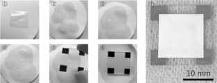
- FIG. 22 shows images of each process when a graphene/porous membrane free-standing laminate was transferred to quartz glass in Example 11 below.
- FIG. 20(1) shows a graphene/porous membrane free-standing laminate placed on a membrane filter.
- FIG. 22(2) and (3) show a state in which the membrane filter placed under the porous membrane is moistened with pure water.
- FIG. 22(4) shows a state in which pure water is dropped onto the graphene membrane of the laminate.
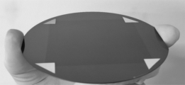
- FIG. 22(5) and (6) show a state in which a 20 mm ⁇ 20 mm quartz substrate with gold/chromium (5 mm ⁇ 5 mm) vapor-deposited on the four corners is placed on the laminate.
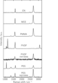
- FIG. 23 is a graph showing the Raman spectrum of the graphene film on a quartz substrate prepared in Example 11 below.
- FIG. 24 shows an optical microscope image obtained during Raman spectroscopy of a graphene film on a quartz substrate prepared in Example 11 below.
- FIG. 25 shows an image of a single-layer graphene film on a SiO 2 /Si substrate prepared in Example 12 below.
- FIG. 26 shows images taken at each step in the transfer process carried out in Example 12 below.
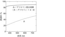
- FIG. 27 is a graph showing the transmittance spectrum of a PVDF/graphene/quartz substrate laminate in a water/glycerin solution measured in Example 13 below.
- One aspect of the present invention provides a laminate comprising a two-dimensional layered material and a porous membrane laminated on the two-dimensional layered material, the laminate being capable of standing on its own in the atmosphere while maintaining its flatness.
- a laminate according to this aspect is shown in Fig. 1.
- the laminate 1 is composed of a two-dimensional layered material 2 and a porous membrane 3.
- the porous film constituting the laminate of the present invention has pores uniformly distributed inside the film, so that the internal stress is evenly distributed without being concentrated locally. The internal stress is relieved by dispersing the internal space, and the stability of the entire structure of the laminate is improved.
- the pores deform to disperse stress against external pressure, so the porous film itself is resistant to deformation.
- porous film is used as a transfer support film.
- porous films such as cellulose mixed ester films and nitrocellulose that can be used in the laminate of the present invention dissolve well in solvents such as acetone, making it possible to obtain a transfer film with very little polymer residue.
- the transfer support material is a porous film, the solvent can easily penetrate into the transfer support material in the process of dissolving the transfer support material, making it possible to quickly and almost completely remove the transfer support material from the two-dimensional layered material.
- two-dimensional layered material refers to a material capable of forming a thin atomic layer.
- two-dimensional layered materials include, but are not limited to, graphene, doped graphene, graphene oxide, hydrogenated graphene, fluorinated graphene, hexagonal boron nitride, molybdenum sulfide, vanadium oxide, silicon, covalent organic frameworks, layered transition metal dichalcogenides (e.g., MoS 2 , TiS 2 , etc.), two-dimensional oxides (e.g., graphene oxide, NiO 2 , etc.), layered group IV and group III-metal chalcogenides (e.g., SnS, PbS, GeS, etc.), silicene, germanene, and layered binary compounds of group IV and group III-V elements (e.g., SiC, GeC, SiGe), etc.
- the two-dimensional layered material may be formed of a single layer or multiple layers.
- a multiple-layer two-dimensional layered material as a transparent conductive film, it is preferable for it to be composed of 2 to 3 layers from the viewpoint of light transparency, but this is not limited to this.
- the two-dimensional layered material is preferably a continuous film.
- a continuous film is a film in which the components constituting the film are continuously connected without any holes or tears.
- the two-dimensional layered material is preferably a continuous film because it has a uniform surface and can reduce sheet resistance.
- the two-dimensional layered material is a continuous film means that the two-dimensional layered material in the laminate is formed and adhered to the porous membrane surface as a continuous film. When the two-dimensional layered material is transferred to the porous membrane surface as a pattern, each of the two-dimensional layered materials constituting the pattern is adhered to the porous membrane surface as a continuous film.
- the laminate of the present invention is capable of transferring the two-dimensional layered material, which is a continuous film, to a desired substrate as a continuous film.
- a two-dimensional layered material is a continuous film when the two-dimensional layered material is transferred to a specific region of the surface of a porous membrane (e.g., the entire surface of the porous membrane or a portion thereof) and the coverage of the specific region is 95% or more.
- the coverage of the two-dimensional layered material is 96% or more, 97% or more, 98% or more, 99% or more, or 99.5% or more.
- the coverage can be measured by transferring a laminate consisting of a two-dimensional layered material/porous film onto a SiO2 /Si substrate, removing the porous film, taking an optical microscope image of the two-dimensional layered material, and calculating the coverage from the color ratio of the single-layer portion in combination with Raman mapping.
- the two-dimensional layered material when referred to as a single layer in this specification, it includes multi-layer two-dimensional layered materials in part, but also includes two-dimensional layered materials that are substantially formed as a single layer.
- a two-dimensional layered material that is substantially formed as a single layer means, for example, that the area of the multi-layer two-dimensional layered material coating on the two-dimensional layered material is 15% or less, 10% or less, 5% or less, or 3% or less.
- the coating rate of the single layer two-dimensional layered material in the two-dimensional layered material is 97% or more.
- the two-dimensional layered material is graphene.
- the graphene film may be doped by substituting carbon atoms of the graphene with nitrogen or boron, or by molecular adsorption.
- metal chlorides or the like may be intercalated between the layers.
- the porous film 3 is laminated on the first surface of the two-dimensional layered material 2.
- the porous film 3 may be laminated so as to cover the entire surface of the two-dimensional layered material 2, or may be laminated so as to cover only a part of the surface. It is preferable that the porous film 3 is capable of supporting the two-dimensional layered material grown on the metal catalyst substrate so that the two-dimensional layered material can maintain its shape in the atmosphere after the metal catalyst substrate is removed by etching in order to transfer the two-dimensional layered material grown on the metal catalyst substrate to a desired substrate.
- the thickness of the porous film 3 is preferably 100 nm or more. If the film thickness is thinner than 100 nm, the support strength of the two-dimensional layered material formed by the CVD method will be insufficient, and there is a high possibility that the material will break during transfer.
- the lower limit of the film thickness of the porous film 3 is 100 nm or more, and in a more preferred embodiment, it is 1 ⁇ m or more. In an even more preferred embodiment, it is 5 ⁇ m or more.
- the upper limit of the film thickness of the porous film 3 is 300 ⁇ m or less, and in a more preferred embodiment, it is 100 ⁇ m or less. If the film is too thick, even if it has a porous structure, the residual stress of the support material will be large, and the quality of the two-dimensional layered material after transfer will be impaired.
- the porous membrane 3 that can be used in the present invention is not limited to the following, but may be a membrane made of a material selected from the group consisting of nitrocellulose, cellulose acetate, polyethersulfone, polytetrafluoroethylene, polyamide, polyvinylidene fluoride, regenerated cellulose, polycarbonate, polypropylene, polyvinylidene chloride, aluminum oxide, glass fiber, quartz fiber, polymethyl methacrylate, polystyrene, polyethylene, polyethylene terephthalate, and ceramic, or a mixed membrane made of two or more materials selected from the group.
- porous membrane that is easily dissolved in a solvent
- the porous membrane 3 may be a laminate of two or more types of porous membranes.
- a mixed membrane made of two or more kinds of materials a cellulose mixed ester, which is a mixture of cellulose acetate and nitrocellulose, can be preferably mentioned.
- the weight ratio in the mixed solution containing cellulose acetate and nitrocellulose used for forming the porous membrane is preferably in the range of 1:1 to 1:3, and more preferably 1:2 or more.
- the porous membrane 3 nitrocellulose, cellulose acetate, and cellulose mixed ester can be preferably mentioned.
- the porous film can be dissolved in a solvent.
- the porous film is a film made of a material that is easily soluble in a solvent, and examples of such porous films include nitrocellulose, cellulose acetate, mixed cellulose esters, polymethyl methacrylate, and polystyrene.
- the use of a porous film that is easily soluble in a solvent can reduce damage to the two-dimensional layered material when the porous film is removed from the two-dimensional layered material after transfer, and is also preferable in that no residue of the porous film remains on the two-dimensional layered material film.
- the average pore size of the porous membrane 3 is preferably 20 nm to 20 ⁇ m. If it is less than 20 nm, the stress relaxation function will decrease, which is undesirable. If it exceeds 20 ⁇ m, the density of the porous membrane will be low, the support force when transferring the two-dimensional layered material will be weak, and the membrane will likely break, which is undesirable.
- the average pore size of the porous membrane 3 is 200 nm to 10 ⁇ m.
- the average pore size of the porous membrane 3 is the average value of the pore sizes of the pores present on the surface of the porous membrane.
- the average value of the pore size of the pores is determined, for example, by observing the surface of the porous membrane using a scanning electron microscope (SEM) or the like, and measuring the area of several hundred randomly selected pores (e.g., 300 pores). From the area of each hole, the diameter assuming that the hole is a circle is calculated as the pore size, and the average value of these can be used as the surface average pore size.
- SEM scanning electron microscope
- the porous membrane 3 preferably has an area ratio of holes to the area of the interface between the two-dimensional layered material and the porous membrane of 20% or more. If the area ratio of holes to the area of the interface between the two-dimensional layered material and the porous membrane is less than 20%, the stress relaxation function decreases and the two-dimensional layered material is easily damaged, which is not preferable.
- the upper limit of the area ratio of holes to the area of the interface between the two-dimensional layered material and the porous membrane is not limited as long as the porous membrane 3 functions as a transfer support membrane for the two-dimensional layered material 2, but can be, for example, 80% or less.
- the area ratio of holes to the area of the interface between the two-dimensional layered material and the porous membrane is 25% or more, and in a more preferred embodiment, the area ratio of holes to the membrane surface is 30% or more.
- the area ratio of holes to the area of the interface between the two-dimensional layered material and the porous membrane of the porous membrane 3 refers to the ratio of the total area of all pores present on one surface of the porous membrane to the geometric area of that surface.
- Those skilled in the art can measure the area of the pores of the two-dimensional layered material by a known method. For example, when the two-dimensional layered material is graphene, the area of the pores is measured by observing the structure of the porous film at the graphene film/porous film interface from the graphene side using a SEM or the like.
- the electrical resistance of the single-layer graphene film in the laminate of the present invention can be 500 ⁇ /sq or less. In a more preferred embodiment, the electrical resistance of the single-layer graphene film is 400 ⁇ /sq or less, 300 ⁇ /sq or less. In an even more preferred embodiment, the electrical resistance of the single-layer graphene film is 200 ⁇ /sq or less. Sheet resistance is the electrical resistance of a substantial conductive film defined as specific resistance/film thickness. The electrical resistance of the laminate can be measured by the van der Pauw method.
- Another aspect of the present invention provides a method for transferring the above laminate to a desired substrate, the method comprising the steps of: (a) A step of adhering the two-dimensional layered material side of the laminate to a desired position on a desired substrate. According to the transfer method of the present invention, it is not necessary to float the two-dimensional layered material on the water surface, and the two-dimensional layered material can be easily transferred to a desired position on a desired substrate.
- the transfer method of the present invention includes the steps of (a) adhering the two-dimensional layered material side of the laminate to a desired position on a desired substrate.
- the "desired substrate” is not limited as long as it is capable of adhering to a two-dimensional layered material and is resistant to a solvent that dissolves a porous film. Examples of such substrates include a transparent insulating substrate and a SiO 2 /Si substrate.
- the shape of the substrate is not limited to a flat surface, and the substrate may have a curved surface.
- the transfer method of the present invention does not require the laminate to float on the water surface in the transfer step, the substrate may be fixed to a building or the like (for example, fixed vertically) like a window glass.
- Transparent insulating substrates that can be used in the present invention include, but are not limited to, quartz, glass, other transparent glass materials, sapphire glass, polyethylene terephthalate, polyester, acrylic resin, polyethylene, nylons, polyvinyl chloride, polyimide, etc.
- the "desired position” refers to the position on the desired substrate to which the two-dimensional layered material is to be transferred.
- the laminate In conventional transfer methods, it was necessary to float the laminate on the water surface and scoop up the laminate with the desired substrate, making it difficult to precisely adjust the transfer position.
- the transfer method of the present invention the laminate itself can stand on its own in the atmosphere, so that it can be easily transferred to the desired position on the substrate.
- a two-dimensional layered material has a large area, it can refer to, for example, 5 cm2 or more.
- the graphene film after transfer using the laminate of the present invention has an area of 10 cm2 or more, more preferably 25 cm2 or more .
- a small amount of a solvent such as water may be dropped onto the two-dimensional layered material side of the laminate and/or the substrate in advance, and the laminate and the substrate may be brought into contact with each other.
- a solvent such as water
- Artificial drying includes, but is not limited to, heating or blowing air using an incubator or a blower.
- the solvent such as water used for bonding the laminate and the substrate is not limited as long as it can promote the bonding by the van der Waals force generated between the laminate and the substrate.
- a solvent it is preferable that it does not have the property of dissolving the porous film and is volatile.
- the solvent include, but are not limited to, water, hexane, heptane, isobutanol, diethyl ether, toluene, etc.
- the laminate of the present invention After transferring the laminate of the present invention to a desired substrate, it may be used without removing the porous film, or it may be used as a two-dimensional layered material with the porous film removed.
- the laminate When used as a laminate consisting of a two-dimensional layered material and a porous film without removing the porous film, it is preferable that the laminate is transparent depending on the target element (substrate). For this reason, the voids in the porous film may be filled with the material that constitutes the porous film, or with another type of material that has the same refractive index as the material that constitutes the porous film. If the porous film does not have an absorption band in the visible light wavelength range, the laminate will be transparent.
- a method of filling the voids in the porous membrane with another type of substance having the same refractive index as the substance that constitutes the porous membrane for example, a method of filling the voids in the porous membrane with a solvent having a refractive index that matches the refractive index of the porous membrane can be mentioned.
- a person skilled in the art can appropriately prepare or adjust a solvent having a refractive index that matches the refractive index of the porous membrane.
- Such a solvent is not limited to the following, but it is possible to combine solvents with different refractive indices, such as a combination of glycerin and water, and adjust the composition ratio to match the refractive index of the porous membrane.
- the transfer method of the present invention can further include, after the step (a), a step (b) of removing the porous film of the laminate using a solvent.
- the solvent for dissolving the porous film can be a known solvent capable of dissolving the porous film, and can be appropriately selected according to the porous film.
- ketones such as acetone and acetic acid, alcohols, or a combination thereof can be used.
- the laminate can be immersed in these solvents, or the laminate can be exposed to the vapor of the solvent by heating these solvents to dissolve and remove the porous film.
- FIG. 2A shows a method of transferring the laminate 1 (porous film/two-dimensional layered material) loaded on the membrane 8 to the substrate 11 by covering the laminate 1 with the substrate 11. More specifically, the laminate 1 loaded on the membrane 8 is moistened with water, and the substrate 11 is bonded onto the laminate 1. The bonded substrate 11, laminate 1, and membrane 8 are turned upside down, and the membrane 8 is further moistened with water. The membrane 8 is then peeled off from the laminate 1 to transfer the laminate 1 to the substrate 11. Thereafter, the porous film 3 in the laminate 1 can be optionally removed to transfer the two-dimensional layered material 2 to the substrate 11.
- the laminate 1 porous film/two-dimensional layered material
- 2B shows a method for transferring the laminate 1 loaded on the membrane 8 onto the substrate 11.
- the desired position of the substrate 11 is moistened with water, and the membrane 8 loaded with the laminate 1 is bonded to the substrate 11 so that the substrate 11 and the porous film 3 in the laminate 1 come into contact with each other.
- the membrane 8 is then further moistened with water, and the laminate 1 is transferred onto the substrate 11 by removing the membrane 8. Thereafter, the two-dimensional layered material 2 can be transferred to the substrate 11 by optionally removing the porous film 3 in the laminate 1.
- 2C shows a method of transferring the laminate 1 directly onto the substrate 11 without using a membrane.
- FIG. 2D shows a schematic diagram of exposing the laminate 1 to acetone vapor to dissolve and remove the porous film 3.
- Another aspect of the present invention provides a method for producing a laminate of a two-dimensional layered material and a porous membrane, the method comprising the steps of: (i) forming a two-dimensional layered material on a metal catalyst substrate by a CVD method; (ii) forming a porous film on the two-dimensional layered material to produce a laminate; and (iii) removing the metal catalyst substrate by etching.
- a PMMA film is formed as a transfer support film on the graphene film formed on a metal catalyst substrate, and the metal catalyst substrate is etched and transferred to a desired substrate, followed by the step of removing the PMMA film.
- the metal catalyst substrate is etched and transferred to a desired substrate, followed by the step of removing the PMMA film.
- the obtained laminate can stand on its own in the atmosphere, and can also retain its shape in the atmosphere after being scooped up from the water surface, so that it is not necessary to perform the etching of the metal catalyst substrate and the transfer to the substrate as a series of steps. In other words, the transfer of the laminate to the desired substrate can be performed at a preferred timing.
- FIG. 3A An example of the scheme of the manufacturing method according to the present invention is shown in FIG. 3A.
- a two-dimensional layered material 2 is formed on a metal catalyst substrate 4, and then a porous membrane forming solution 3' is applied to the two-dimensional layered material 2 by an applicator.
- the obtained laminate is transferred to a water tank containing ultrapure water to promote the formation of a porous membrane.
- the obtained laminate 1'' (porous membrane/two-dimensional layered material/metal catalyst substrate; wet state) is dried, and the dried laminate 1' (porous membrane/two-dimensional layered material/metal catalyst substrate) is floated in an etching solution in an etching tank to etch the metal catalyst substrate.
- the laminate 1 can be produced by recovering the laminate 1 from the etching solution. In the embodiment shown in FIG. 3A, the laminate 1 is recovered using a membrane 8.
- FIG. 3B A manufacturing scheme of a graphene electrode using a conventional transfer support film is shown in Fig. 3B.
- the conventional graphene film transfer method using PMMA as a transfer support film it is necessary to scoop up the PMMA laminate (PMMA/graphene film) directly from the etching tank 7 (water tank for subsequent cleaning) with a substrate 11. After the PMMA laminate 10' is scooped up with the substrate 11, the PMMA is removed.
- PMMA residue is generated on the graphene film surface after PMMA removal. Such residue has an undesirable effect on the properties of the graphene film.
- the manufacturing method of the present invention can use a porous film that is easily dissolved by a solvent, and in this case, the above problem can be avoided.
- the method for manufacturing a laminate according to the present invention includes (i) a step of forming a two-dimensional layered material on a metal catalyst substrate by a CVD method.
- the method of forming a two-dimensional layered material 2 on a metal catalyst substrate 15 by a CVD method is known, and can be carried out by referring to, for example, the above-mentioned Reference 1.
- the metal catalyst substrate 15 that can be used in the present invention is not limited, and any known substrate used for forming a two-dimensional layered material 2 can be used. Preferred examples include copper substrates, nickel substrates, cobalt substrates, iridium substrates, platinum substrates, gold substrates, and alloy substrates thereof. A substrate in which these metals are vapor-deposited on a heat-resistant substrate may also be used.
- a further step of (ii) forming a porous membrane on the two-dimensional layered material is carried out.
- the method for forming the porous film 3 on the two-dimensional layered material is not limited, and known methods such as spin coating, spray coating, phase inversion using an applicator or bar coater, vapor deposition, etc. The method for forming a porous film by spin coating will be described below.
- a polymer serving as a raw material for the porous membrane 3 is dissolved in a solvent to prepare a solution for forming the porous membrane.
- An appropriate polymer can be selected depending on the porous membrane 3 to be formed.
- the polymer used to form the porous membrane 3 may be one type, or two or more types may be used. It is known that when forming the porous film 3 by spin coating, the thickness and average pore size of the porous film change depending on the conditions such as the selection of the solvent, the concentration of the polymer in the solvent, the rotation speed of the spin coater, the viscosity of the solution, and the average molecular weight of the polymer (affects the viscosity).
- the solvent is not limited as long as it can dissolve the polymer and can form a porous film by spin coating.
- acetone, methanol, diethyl ether, ethyl acetate, etc. can be used as the solvent.
- the solvent is preferably a low boiling point solvent.
- the solvent has a boiling point of 100°C or less, and in a more preferred embodiment, the solvent has a boiling point of 80°C or less.
- the evaporation rate of a low boiling point solvent is fast, so that the precipitation rate of the polymer in the solution is high, and the polymer is randomly precipitated to form a porous structure, which is preferable.
- the concentration of the polymer in the solvent can be from 0.5 to 20% by weight.
- a laminate of a metal catalyst substrate 15 and a graphene film 2 is fixed on a spin coater stage, and the prepared porous film forming solution is dropped onto the surface and near the center of the graphene film 2.
- the amount of the porous film forming solution to be dropped may be an amount sufficient to sufficiently cover the graphene film 2.
- the rotation speed and rotation time of the spin coater are not limited as long as the desired porous film can be formed.
- the rotation speed can be 200 to 5000 rpm, and the rotation time of the spin coater can be 10 to 120 seconds. Thereafter, if any solvent remains, drying is performed by heating.
- the porous film 3 can be formed on the two-dimensional layered material by casting using an applicator or the like and by a phase inversion method.
- Phase inversion is a method of making materials such as polymers porous by inverting the phase from a liquid state to a solid state under certain controlled conditions.
- Representative phase inversion methods include nonsolvent-induced phase separation and thermally induced phase separation.
- the solvent in a polymer solution containing a nonsolvent or poor solvent evaporates, making the polymer solution unstable, resulting in the polymer precipitating in the presence of a nonsolvent, and in the nonsolvent contacting the polymer, the solvent in the polymer solution is extracted into the nonsolvent, and at the same time, the nonsolvent enters the polymer solution, making the polymer solution unstable and resulting in the polymer precipitating.
- the former is called the dry phase inversion method
- the latter is called the wet phase inversion method.
- the method of forming a porous film by the phase inversion method is known, and reference can be made to, for example, Masahiro Tamura, Tadashi Uragami, Mizuho Sugihara, “Permeation Characteristics on Cellulose Nitrate-Cellulose Acetate Blend Polymer Membranes,” Journal of the Japan Society of Colour Material Vol. 50 (6), 317-322 (1977).
- the non-solvent induced phase separation method forms a porous structure by utilizing a solvent exchange process between a good solvent and a poor solvent in a liquid phase, so that a porous film can be formed without causing excessive volume shrinkage due to rapid solvent evaporation, and damage to graphene at the contact interface with graphene that occurs during the formation of the porous film can be reduced.
- the solvent used in the phase inversion method may be the same as that used in the spin coating method, and the concentration of the polymer in the solvent may be 0.5 to 20% by mass.
- a step (iii) of removing the metal catalyst substrate by etching is performed.
- a known method can be adopted to remove the metal catalyst substrate 15.
- etching can be performed with a known solution such as an aqueous ammonium persulfate solution or an aqueous iron (III) nitrate solution.
- Etching can be performed by floating the laminate on the surface of the etching solution so that the copper foil surface comes into contact with the etching solution.
- the laminate may be immersed in the etching solution to etch the metal catalyst substrate. Since the laminate of the present invention has high mechanical strength, it can maintain a low sheet resistance even when immersed in an etching solution.
- the two-dimensional layered material on the back side is removed using oxygen plasma treatment or the like before etching the metal catalyst substrate 15.
- the porous film 3/two-dimensional layered material 2/metal catalyst substrate 15 is floated in the etching solution so that the surface from which the two-dimensional layered material has been removed is in contact with the etching solution, and the metal catalyst substrate 15 is removed.
- the laminate consisting of the porous film 3 and the two-dimensional layered material 2 is washed by moving it to the water surface of a pure water pool. It is preferable to perform the washing process three or more times.
- the laminate 1 floating on this pure water is scooped up with any membrane or the like. After scooping up, the laminate 1 is dried to complete the production of the laminate.
- Example 1 Production of a laminate consisting of a graphene film and a porous film
- a laminate consisting of a single-layer graphene film and a cellulose film (porous film) (hereinafter also referred to as a "porous film/graphene laminate”) was produced as follows.
- a copper foil (thickness 35 ⁇ m) was prepared as a metal catalyst substrate for the growth of graphene chemical vapor deposition (CVD). Prior to the formation of a graphene film by CVD, the copper foil was immersed in pure water, ethanol, and acetone in that order, and ultrasonic treatment was performed to clean the copper foil surface.
- the copper foil was then transferred to a thermal CVD furnace, hydrogen was introduced, and hydrogen annealing of the copper substrate was performed for 30 minutes under conditions of a hydrogen atmosphere total pressure of 700 Pa and 1000° C. Then, methane was introduced, and graphene was grown by CVD for 10 minutes at a flow rate of 2 sccm methane and 20 sccm hydrogen at 1000° C. and a total pressure of 750 Pa.
- a porous film was fabricated on a graphene film formed on a copper foil using a spin coating method.
- Nitrocellulose (CN), cellulose acetate (CA), or a mixed membrane of nitrocellulose and cellulose acetate (cellulose mixed membrane) was used as the support layer for graphene transfer.
- Nitrocellulose (Nacalai Tesque, product number 24728-34), cellulose acetate (Sigma-Aldrich, product number 419028), and a solvent, acetone, were prepared as raw materials for the solution for forming the porous membrane.
- Cellulose acetate or nitrocellulose and acetone were mixed so that the content of cellulose acetate or nitrocellulose was 2 mass% to prepare a solution for forming the porous membrane.
- nitrocellulose, cellulose acetate, and acetone were mixed to prepare three types of cellulose mixed solutions with different compositions so that the total content of both nitrocellulose and cellulose acetate was 2 mass% and the mass ratios of nitrocellulose and cellulose acetate were 3:1, 1:1, and 1:3.
- a PMMA solution that has been used as a support membrane for conventional graphene transfer was prepared.
- a PMMA solution (Sigma-Aldrich, product number 182265) was prepared by dissolving PMMA in a solvent, ethyl lactate, so that the content of PMMA was 4 mass %.
- a solution for forming a porous film was dropped onto the graphene film formed on the copper foil, and spin-coated at 2000 rpm to form a nitrocellulose film, a cellulose acetate film, or a cellulose mixed ester film.
- a PMMA film which is a transfer support film, was formed on the graphene film formed on the copper foil.
- the unnecessary graphene film formed on the back side of the copper foil was removed by oxygen plasma treatment. This resulted in a laminate consisting of a porous film/graphene film/copper foil.
- a laminate consisting of a PMMA film (transfer support film)/graphene film/copper foil was obtained as a comparative example.
- An etching tank was prepared, and a copper etching solution of an aqueous solution of iron (III) nitrate (0.5 mol/L) was stored in the tank at 25°C.
- the size of the laminate consisting of a porous film/graphene film/copper foil to be copper etched was 15 mm x 10 mm.
- the laminate was floated in the copper etching solution so that the copper foil was in contact with the solution, and the copper foil of the laminate was removed by etching for 5 hours. In this way, a porous film/graphene film laminate comprising a porous film and a graphene film was obtained. Also, a PMMA film (transfer support film)/graphene film laminate was obtained as a comparative example.
- the porous membrane surface of the prepared porous membrane/graphene membrane laminate was observed using a SEM (FE-SEM, manufactured by ZEISS), and the pore diameter and the ratio of the surface occupied by the pores were measured from the SEM images.
- the sample used for SEM observation was a sample in which the porous membrane surface of the porous membrane/graphene membrane laminate formed on the copper foil after spin coating was coated with 3 nm of platinum.
- the surface of the PMMA membrane was also observed as a comparative example. SEM images are shown in Figure 4.
- the PMMA membrane had a smooth surface and formed a dense membrane structure without holes.
- the CN membrane and CA membrane had holes, but they were composed of small pores, and no holes of a size of 100 nm or more were observed.
- the CA membrane also had a surface with a low density of holes. All of the prepared cellulose mixed membranes had a porous structure, and a tendency was observed in which the pore diameter increased as the mass ratio of nitrocellulose increased. The diameters of all holes visible in the SEM images were estimated based on the scale bar. From the pore diameter data, the surface occupancy of the pores, which is the area ratio of the pores to the membrane surface of the porous membrane in the CN membrane, was calculated. For the mixed membrane, the proportion of the black area after converting the SEM image to a black and white image was calculated as the surface occupancy of the pores. Figures 5 and 6 show the pore size distribution (histogram) of each sample.
- the histogram was created from the diameter values of all pores recognizable on the SEM image of Figure 4. Therefore, the histograms are shown for the PMMA membrane in which no pores were observed and the CA membrane with low pore density.
- the CN membrane had only pores with a diameter of 40 nm or less, and the average pore diameter was 17 nm.
- the surface occupancy of the pores in the CN membrane was 2.1%.
- Example 2 Production of a laminate consisting of a porous film, a graphene film, and a transparent insulating substrate
- the porous film/graphene film laminate produced in Example 1 was transferred onto a transparent insulating substrate to produce a laminate consisting of a porous film, a graphene film, and a transparent insulating substrate.
- a quartz substrate (1 mm thick, 20 mm x 20 mm) was prepared as a transparent insulating substrate. Chromium was deposited to a thickness of 10 nm on a part of the quartz substrate using a vacuum deposition apparatus, and gold was deposited to a thickness of 50 nm on the chromium.
- This metal deposition film functions as a conductive electrode when a porous film/graphene film laminate is laminated on the quartz substrate, and is necessary when the transferred graphene film is used as a device such as an electrode for electrochemical measurement.
- a water tank filled with ultrapure water was prepared. After copper etching, the porous film/graphene film laminate floating in the etching solution was transferred to the water surface of the water tank and washed with water. The laminate was repeatedly washed by transferring it to another water tank. This washing process was performed three times. The porous film/graphene film laminate floating in the ultrapure water pool was scooped up using a quartz substrate on which chromium and gold had been vapor-deposited in advance as a conductive electrode.
- the porous film/graphene film laminate was laminated so that a part of the conductive electrode overlapped with a part of the porous film/graphene film laminate.
- a laminate consisting of a quartz substrate, which is a transparent insulating substrate, a porous film, and a graphene film was produced.
- the thickness of the porous film on the laminate was measured using a stylus step gauge (manufactured by BRUKER).
- the thickness of the laminate manufactured using an ethyl lactate solution containing 4% by mass PMMA was approximately 150 nm.
- Example 3 Preparation of free-standing graphene/porous film laminate
- ADVANTEC model number: A045A047A
- Example 4. Verification of transfer support ability of porous membrane the transfer support ability of the porous film in the etching process of the metal catalyst substrate and the subsequent transfer process to the transparent insulating substrate was examined.
- a porous film was formed on the graphene film under the same conditions as in Example 1, except that an acetone solution with a concentration of 1 mass% nitrocellulose was used.
- the thickness of the porous film formed on the graphene film was less than 100 nm.
- a porous film was formed on the graphene film under the same conditions as in Example 1, except that an acetone solution with a nitrocellulose concentration of 6 mass% or a cellulose acetate concentration of 4 mass% was used.
- the thickness of the porous film formed on the graphene film was 1 ⁇ m or more.
- the graphene film was able to be supported, but after transfer to the quartz substrate, some peeling from the quartz substrate was observed.
- a PET substrate was used instead of the quartz substrate, no peeling occurred even when the porous film had a thickness of 1 ⁇ m or more.
- FIG. 8 shows an SEM image of the surface of the cellulose mixed ester film that was dried after casting (platinum coated to suppress charge-up).
- the acetone solvent was used, no pore structure was observed, whereas when the acetone + formamide solvent was used, a pore structure was observed.
- Acetone is a good solvent for CA and CN, while formamide is a good solvent only for CN and a poor solvent for CA.
- FIG. 9 shows SEM images of the surface of the six types of cellulose mixed ester membranes produced ((a) without 4% immersion, (b) with 4% immersion, (c) without 8% immersion, (d) with 8% immersion, (e) without 12% immersion, (f) with 12% immersion).
- the pore diameter tended to increase when immersed in water. This is because the dissolved solvent in the casting solution was exchanged for water by gelling the casting solution through immersion in water, resulting in phase inversion.
- the thickness of the porous membrane measured by DekTak is shown in Table 1.
- the film thickness measurement results showed that the film thickness tends to increase with increasing solute concentration and immersion in water.
- the significant increase in the thickness of the porous film by immersion in water indicates that the sample immersed in water contains many voids.
- the film thickness can be said to increase because the amount of solute contained in the casting liquid increases with increasing solute concentration.
- the significant increase in film thickness in the sample immersed in 12% water is thought to be related to the viscosity of the porous film forming solution.
- the increased viscosity reduces the fluidity of the solute and suppresses the aggregation of solutes, which is thought to suppress the shrinkage of the porous film thickness relative to the applicator gap.
- Table 2 shows the viscosity of the porous film forming solution measured with a viscometer (Anton Paar, model number: ViscoQC 100, spindle: SC4-21).
- the tensile stress also increases in the samples made using an applicator because the thickness increased compared to the spin coating method. While the mixed cellulose ester film made from the acetone solvent solution did not form a porous structure, the acetone/formamide mixed solvent formed a porous structure throughout the entire inside of the film, and this tensile stress was relaxed and no peeling occurred. It was found that by making the support film porous in this way, it was possible to transfer the support film/graphene laminate to the substrate without peeling even if the thickness was 10 ⁇ m or more.
- FIG. 10(a) shows the Raman spectrum of a porous cellulose mixed ester film/graphene laminate transferred onto a quartz substrate using a support film prepared by immersing in pure water using a solution with a solute concentration of 12% by mass. Peaks derived from cellulose CH 3 and C—H appearing near 1280 cm ⁇ 1 and 2950 cm ⁇ 1 were observed, but the 2D peak and G peak derived from graphene were not observed. This is thought to be because the support film was porous and thick, so the laser light was scattered by the support film and did not reach the graphene.
- FIG. 10(b) shows the Raman spectrum of graphene after removing the support film.
- the 2D peak and G peak derived from graphene were observed, and the D peak indicating defects appearing near 1350 cm ⁇ 1 was hardly observed, so it can be said that high-quality graphene could be produced even when the cellulose mixed ester film prepared by the casting method was used as the support material.
- no peak due to C--H of cellulose was observed near 2950 cm -1 , which indicates that the cellulose mixed ester was completely removed by immersion in hot acetone.
- Example 6 Preparation of mixed cellulose ester membrane by phase inversion method: thickness change 1
- a solution of 12% by mass of cellulose mixed ester with cellulose acetate: nitrocellulose in a mass ratio of 2:1 in acetone-formamide (mass ratio of acetone: formamide: 1:1) was used to prepare a porous film under the conditions of a four-sided applicator (width 60 mm) with a gap height of 25, 50, 75, and 100 ⁇ m.
- Graphene was grown on copper foil in the same manner as in Example 1.
- the running speed during film formation was set to 2 mm/s, and four types of porous film samples with different thicknesses were formed on graphene grown on copper foil.
- the viscosity of the solution was high (609 mPa ⁇ s), and drying began immediately after spreading on the graphene, so the solution did not spread any further after spreading with the applicator.
- the copper foil after applying the cellulose solution was transferred to a pure water pool and immersed for 1 hour, and then naturally dried after being removed from the pure water.
- the film surface was observed by SEM in the same manner as in Example 1, and the average pore size and the surface occupancy rate of the pores were calculated from the captured image.
- the film thickness was measured by a laser microscope.
- FIG. 11 shows an SEM image of the cellulose mixed ester film. When comparing the respective samples, it was observed that the cellulose fiber structure becomes thicker as the film thickness increases.
- Table 3 shows the film thickness, the average pore size of the pores on the film surface, and the surface occupancy rate of the pores.
- Example 7 Preparation of cellulose mixed ester membrane by phase inversion method - thickness change 2
- a cellulose mixed ester was prepared by the phase inversion method using the same solution as in Example 6 and a multi-vaporized applicator (Cortek, width 100 mm, model number: MA100) under the condition of gap heights of 100, 200, 300, and 400 ⁇ m.
- a porous film was prepared on a copper foil on which graphene was not grown.
- the coating conditions by the applicator were the same as those in Example 6, except for the type of applicator, gap height, and running speed.
- the running speed of the applicator in this example was 15 mm/s.
- FIG. 12 A photograph of a sample coated with a solution at a gap height of 300 ⁇ m, immersed in pure water, and dried is shown in FIG. 12.
- the copper foil of the substrate was significantly warped, suggesting that the tensile stress in the porous film increased due to the increase in film thickness.
- samples with a gap height of 200 ⁇ m or more warping of the copper foil and peeling of some of the porous film were observed.
- the samples with a gap height of 100 ⁇ m almost no warping of the copper foil was observed.
- the film thickness measured by a laser microscope was 37 ⁇ m for the sample prepared with a gap height of 100 ⁇ m, 75 ⁇ m for the sample prepared with a gap height of 200 ⁇ m, and 157 ⁇ m for the sample prepared with a gap height of 300 ⁇ m.
- FIG. 14 shows a photograph of the porous film after immersion in water and drying. It can be seen that the warping of the copper foil increases as the gap height increases. Since the 400 ⁇ m sample cracked, three types of samples, 100, 200, and 300 ⁇ m, were cut to 20 mm x 20 mm and transferred to a slide glass. Even after washing with pure water and drying, the laminate did not peel off from the slide glass.
- Example 8 Study of polymer materials suitable for porous membranes for supporting graphene transfer
- Six types of polymers were cast onto graphene grown on copper foil by CVD, and porous structures were created by phase inversion. To confirm whether the polymer film formed a porous structure, SEM observations of the polymer film/graphene laminate were performed.
- the polymer films used were cellulose acetate (CA), nitrocellulose (CN), mixed cellulose ester (MCE), polymethyl methacrylate (PMMA), polyvinylidene fluoride (PVDF), and polyethersulfone (PES).
- CA cellulose acetate
- CN nitrocellulose
- MCE mixed cellulose ester
- PMMA polymethyl methacrylate
- PVDF polyvinylidene fluoride
- PES polyethersulfone
- the copper foil was cut to 110 mm x 70 mm and immersed in acetic acid for 3 minutes, then in pure water and acetone, and then dried by nitrogen blowing.
- the copper foil was then transferred to a thermal CVD furnace, hydrogen was introduced, and hydrogen annealing of the copper substrate was performed for 30 minutes under conditions of a hydrogen atmosphere total pressure of 700 Pa and 1000°C.
- Methane was then introduced, and graphene was grown by CVD for 10 minutes at a flow rate of 2 sccm methane and 20 sccm hydrogen at 1000°C and a total pressure of 750 Pa.
- the copper foil on which graphene was grown was cut to 110 mm x 35 mm. This CVD process was performed three times, and six sheets of copper foil on which graphene was grown were prepared, each measuring 110 mm x 35 mm.
- compositions of the solutions for preparing various polymer films are shown in Table 4.
- the raw materials of the polymer materials shown in Table 4 were weighed into a vial, and the solvent was added and stirred. PVDF and PES were difficult to dissolve, so they were kept at 55°C until they were dissolved.
- the copper foil (110 mm x 35 mm) on which graphene was grown was fixed to the stage by the clamp function of a fully automatic linear motion coater, and the solution was applied to the graphene/copper foil using a multi-vaporized applicator.
- the gap height of the applicator was set to 160 ⁇ m as measured by the attached micrometer. Since the thickness of the copper foil was 35 ⁇ m, the gap height between the copper foil and the applicator is thought to be about 125 ⁇ m.
- the running speed of the applicator was set to 15 mm/s.
- the graphene/copper foil to which the various solutions were applied was immediately immersed in a pool of pure water and removed after 30 minutes. After removing from the pool of pure water, the polymer attached to the graphene on the back side of the copper foil was removed with a cotton swab moistened with various solvents, and the graphene on the back side of the copper foil was removed by exposing it to oxygen plasma. Then, the sample was cut to 15 mm x 15 mm. Photographs of six types of samples are shown in Figure 15. The four types of samples coated with PVDF, PES, CN, and MCE were white, suggesting the formation of a porous structure.
- the color of the copper foil was strong in the samples coated with CA and PMMA, so it is believed that the polymer support film was almost transparent and no porous structure was formed.
- Platinum was coated on the polymer film side of this polymer film/graphene/copper foil laminate, and SEM observation was performed. SEM images are shown in Figures 16 and 17. Holes were observed in all polymer films, but the holes on the surface of CA, PMMA, and PES were small, and the proportion of the surface occupied by the holes was small. Since PES is white, it is believed that a skin layer was formed on the surface. As for the other three types, the proportion of the surface occupied by the holes was small, so it is believed that the film became thicker due to the high applicator gap and a skin layer was formed.
- Example 9 Transfer of laminate by conventional method and measurement of laminate thickness
- the 15 mm x 15 mm polymer support film/graphene/copper foil laminate produced in Example 8 was floated in a 10 mass % ammonium persulfate aqueous solution, which is a copper etching solution, with the copper facing down.
- a 10 mass % ammonium persulfate aqueous solution which is a copper etching solution
- the polymer support film/graphene laminate floating in the etching solution was transferred to the water surface of a water tank and washed with water.
- the laminate was repeatedly washed by transferring it to another water tank. This washing process was performed three times.
- the porous film/graphene film laminate floating in a pure water pool was scooped up using a quartz substrate.
- FIG. 18 shows a photograph of the polymer support film/graphene laminate transferred onto a quartz substrate.
- the CA/graphene laminate peeled off from the quartz substrate during the drying process.
- the photograph of CA shows some translucent areas, suggesting that it has a partially porous structure, but most of it is transparent and a sufficient porous structure was not formed, which resulted in tensile stress, and it can be said that the stress exceeded the adhesive force between the quartz substrate and the graphene.
- the PMMA/graphene laminate had higher transparency than the other four types of support film/graphene laminates other than CA, but the entire film was uniformly translucent.
- the thickness of the support film/graphene laminate transferred onto the quartz substrate was measured using a shape analysis laser microscope (Keyence, VK-X1000). Table 5 shows the thickness of the five types of laminate. The thickness of the CA film could not be measured because it could not be transferred to the substrate. The difference in thickness between samples even with the same applicator gap height is related to the solute concentration, viscosity of the solution, and the degree of formation of the porous structure.
- Example 10 Preparation of graphene/porous support membrane free-standing laminate and structural evaluation by SEM
- the 15 mm x 15 mm polymer support film/graphene/copper foil laminate produced in Example 8 was floated in a 10 mass% ammonium persulfate aqueous solution, which is a copper etching solution, with the copper facing down, as in Example 8. After all the copper was etched, the graphene/polymer support film laminate floating in the aqueous solution was scooped up onto a cellulose mixed ester membrane filter (ADVANTEC, model number: A045A047A) so that the support film and the membrane filter were in contact as shown in FIG. 19.
- ADVANTEC model number: A045A047A
- the membrane filter portion of this laminate was grasped with tweezers, and the membrane filter to which the polymer film/graphene laminate was attached was immersed in a pool of pure water to wash the polymer film/graphene laminate. At this time, the laminate was separated from the membrane so that the porous side was in contact with the water surface, and it was possible to float on the water surface with the graphene facing up. After washing in a water tank, the membrane was again scooped up so that the membrane and the porous membrane were in contact. The laminate floating in the water tank could be easily transferred to the membrane.
- FIG 20 shows a photograph of a graphene/polymer support film laminate placed on a membrane.
- the laminate using PMMA as a support material had some thin white parts, but most of them were transparent.
- the graphene surfaces of five types of graphene/polymer support film laminates were observed by SEM.
- Figure 21 shows an SEM image. All of the polymer materials used for the transfer support film are electrically insulating, but since graphene is transferred, charge-up can be avoided.
- Example 11 Transfer of graphene/porous support film free-standing laminate and four-terminal resistance measurement
- the graphene/porous membrane free-standing laminate prepared in Example 10 was transferred to quartz glass on which gold/chromium was vapor-deposited by the method shown in FIG. 22.
- the membrane filter placed under the porous support membrane of the graphene/porous support membrane free-standing laminate (FIG. 22(1)) placed on the membrane filter shown in FIG. 20 was moistened with pure water (FIG. 22(2) and (3)), and then pure water was dropped onto the graphene membrane of the laminate (FIG.
- a typical CVD graphene transfer process includes a step of scooping up a support film/graphene laminate floating on the surface of a pure water pool, as in Example 2.
- graphene can be easily transferred to any position on any substrate without the need to float it on water.
- the electrical properties of the graphene produced using five types of graphene/porous support film freestanding laminates were measured using electrical resistance measurements by the van der Pauw method and a Hall effect measurement device (Nanometrics). After measuring the electrical properties, the support film was immersed in acetone in an attempt to dissolve. CN, MCE, and PMMA could be removed, but PES and PVDF could not be completely dissolved and removed. Hall effect measurements and Raman spectroscopy measurements were also performed on the samples after the support film had been dissolved.
- Graphene transferred using CN and MCE as support materials maintained high electrical conductivity without any breaks over almost the entire surface even after immersion in acetone. Both samples had sheet resistances below 200 ⁇ /sq, which is an extremely low value for single-layer graphene. This low sheet resistance is proof that high-quality graphene without breaks was transferred. Residues were visually confirmed after acetone immersion in the PMMA-supported transfer sample, and were not removed even when immersed in hot acetone. Optical microscope images after acetone immersion showed that most of the graphene was broken. From the SEM image in Figure 21, it is believed that the frequent breaks were caused by the formation of a thick film with insufficient porosity, which generated large tensile stress. It is believed that the residues that were not dissolved in hot acetone were generated because PMMA wrapped in broken graphene remained on the substrate surface.
- porous films of MCE or CN are the optimal support material for transferring graphene, as their porous structure does not generate stress and they are easily dissolved after graphene is transferred. Furthermore, because the laminate with graphene is self-supporting, it has been demonstrated that high-quality graphene can be transferred using a simple method that was not previously possible. This invention is extremely valuable in terms of the industrial application of graphene, and is expected to be of great help in promoting research into the use of graphene.
- Example 12 Large-area graphene transfer using a porous membrane/graphene laminate
- a laminate consisting of a single-layer graphene film and a cellulose film (porous film) (hereinafter also referred to as a porous film/graphene laminate) was produced as follows. Copper foil (65 mm x 90 mm, thickness 35 ⁇ m) was prepared as a metal catalyst substrate for the growth of graphene chemical vapor deposition (CVD), and graphene film formation by CVD was performed in the same manner as in Example 8. Before forming the graphene film, the copper foil was immersed in pure water, ethanol, and acetone in that order, and ultrasonic treatment was performed to clean the copper foil surface.
- CVD graphene chemical vapor deposition
- the copper foil was transferred to a thermal CVD furnace, hydrogen was introduced, and hydrogen annealing of the copper substrate was performed for 30 minutes under conditions of a hydrogen atmosphere total pressure of 700 Pa and 1000 ° C. Then, methane was introduced, and graphene was grown by CVD for 10 minutes at a flow rate of 2 sccm methane and 20 sccm hydrogen at 1000 ° C. and a total pressure of 750 Pa.
- a phase inversion method was used to fabricate a porous film on a graphene film formed on a copper foil.
- a mixed membrane (cellulose mixed membrane) of nitrocellulose (CN) and cellulose acetate (CA) was used as the support layer for graphene transfer.
- Nitrocellulose Nacalai Tesque, product number 24728-34
- cellulose acetate Sigma-Aldrich, product number 419028
- solvents acetone and formamide were prepared as raw materials for the solution for forming the porous membrane.
- the solution for forming the porous membrane was prepared by dissolving cellulose acetate and nitrocellulose in a mixed solvent of acetone and formamide at a mass ratio of 1:1 so that the cellulose acetate content was 4 mass% and the nitrocellulose content was 8 mass%.
- the copper foil having a surface on which a graphene film was formed by the CVD method was fixed to the stage of a fully automatic linear motion coater, and a solution was uniformly spread on the graphene using a multi-vaporized applicator (width 100 mm) under conditions of a gap height of 100 ⁇ m and a running speed of 15 mm/s.
- the graphene/copper foil laminate on which the solution was spread by the applicator was immersed in a pure water pool and left at room temperature for 1 hour.
- the graphene/copper foil laminate on which the porous film was formed was removed from the pure water pool and dried at room temperature, and then the graphene film formed on the copper foil on the opposite side to the surface on which the porous film was formed was removed by oxygen plasma treatment.
- the laminate consisting of the porous film/graphene/copper foil was cut to 65 mm x 65 mm.
- the laminate thus produced had a thickness of 10 ⁇ m or more and was strong enough not to break even when removed from the pure water. After removing this laminate from the pure water, it was placed on a 90 mm diameter membrane filter (ADVANTEC, model number: A045A090C) so that the porous membrane side was in contact with the membrane surface and dried at room temperature. The obtained laminate was able to stand on its own in the air without irreversible deformation.
- the laminate After drying the laminate and the membrane filter, the laminate is peeled off from the membrane, and only the laminate can be handled.
- pure water is dropped onto the substrate, and then the laminate together with the membrane filter is placed at a desired position on the substrate so that the graphene film of the laminate is on the SiO 2 /Si substrate side.
- the four corners of the graphene are arranged so as to contact the four chromium/gold parts vapor-deposited on the SiO 2 /Si.
- FIG. 25 shows a photograph of the single-layer graphene after dissolving the cellulose mixed ester support film.
- the oxide film (SiO 2 ) layer of the SiO 2 /Si substrate used in this example had a thickness of 300 nm, which is an oxide thickness suitable for visualizing single-layer graphene, and it was confirmed that a large-sized graphene of 65 mm x 65 mm was transferred. In addition, it showed a uniform color and no change in color due to residue was observed, which shows that this transfer method is an excellent method with very little graphene breakage or support material residue.
- the sheet resistance measured by the van der Pauw method was 354 ⁇ /sq. The fact that such a low sheet resistance was obtained indicates that the graphene/porous film laminate according to the present invention can transfer even large-area graphene with very little breakage.
- FIG. 26 shows images taken at each step in the transfer process of this example.
- Example 13 Making porous film/graphene laminate transfer film transparent
- a PVDF/graphene laminate electrode was prepared by a casting method using an applicator with a gap height of 100 ⁇ m in the same manner as in Example 9.
- the PVDF porous membrane-forming solution was prepared by dissolving PVDF (Sigma-Aldrich, product number: 347078) in a mixed solvent of acetone/dimethylformamide (DMF) with a mass ratio of 1:1 to 12 mass%.
- the prepared PVDF/graphene/quartz substrate laminate was immersed in methanol for hydrophilization treatment, and then impregnated with water or a water/glycerin solution and a cover glass was placed on it to measure the transmittance.
- the transmittance spectrum is shown in FIG.
- Example 14 Evaluation by Raman mapping of graphene transferred by a transfer method using a porous film/graphene laminate
- a 20 mm x 20 mm cellulose mixed ester/graphene laminate prepared by the casting method was transferred to a 20 mm x 20 mm quartz glass substrate using an applicator with a gap height of 100 ⁇ m.
- the graphene on the quartz substrate after removing the porous film using acetone vapor was subjected to Raman mapping using a WITec Raman imaging microscope alpha300 to examine the coverage of graphene.
- the measurement conditions were as follows: 20 mm x 20 mm of the entire quartz substrate was measured every 1 mm vertically and horizontally to obtain a mapping image of 20 squares x 20 squares. The measurement was also performed using an autofocus function. The presence of graphene was determined by the presence or absence of a 2D peak. Of the 361 squares (19 x 19) excluding the outermost squares of the mapping image, one square did not observe a 2D peak, and one square observed a cellulose peak. Therefore, it was confirmed that 99% or more of the transferred graphene was graphene without support film residues and tears.
- Laminate (porous membrane/two-dimensional layered material) 1' Laminate (porous membrane/two-dimensional layered material/metal catalyst substrate) 1'' Laminate (porous membrane/two-dimensional layered material/metal catalyst substrate; wet state) 2 Two-dimensional layered material 3 Porous film 3' Porous film forming solution 4 Metal catalyst substrate 5 Applicator 6 Water tank 7 Etching tank 8 Membrane 9 PMMA 10 PMMA laminate (PMMA/graphene film/metal catalyst substrate) 10' PMMA laminate (PMMA/graphene film) 11 Substrate
Landscapes
- Chemical & Material Sciences (AREA)
- Health & Medical Sciences (AREA)
- Engineering & Computer Science (AREA)
- Immunology (AREA)
- Life Sciences & Earth Sciences (AREA)
- Biomedical Technology (AREA)
- Urology & Nephrology (AREA)
- Molecular Biology (AREA)
- Hematology (AREA)
- Organic Chemistry (AREA)
- Inorganic Chemistry (AREA)
- Materials Engineering (AREA)
- Ceramic Engineering (AREA)
- Analytical Chemistry (AREA)
- Medicinal Chemistry (AREA)
- Biotechnology (AREA)
- Cell Biology (AREA)
- Pathology (AREA)
- Microbiology (AREA)
- General Physics & Mathematics (AREA)
- General Health & Medical Sciences (AREA)
- Food Science & Technology (AREA)
- Biochemistry (AREA)
- Physics & Mathematics (AREA)
- General Chemical & Material Sciences (AREA)
- Nanotechnology (AREA)
- Chemical Kinetics & Catalysis (AREA)
- Mechanical Engineering (AREA)
- Metallurgy (AREA)
- Carbon And Carbon Compounds (AREA)
- Laminated Bodies (AREA)
- Investigating Or Analysing Materials By The Use Of Chemical Reactions (AREA)
Priority Applications (4)
| Application Number | Priority Date | Filing Date | Title |
|---|---|---|---|
| JP2025510795A JPWO2024203971A1 (https=) | 2023-03-24 | 2024-03-23 | |
| CN202480034789.4A CN121219128A (zh) | 2023-03-24 | 2024-03-23 | 包括二维层状材料及多孔质膜的叠层体、该叠层体的转移方法及其制造方法 |
| EP24780089.9A EP4696494A1 (en) | 2023-03-24 | 2024-03-23 | Laminate comprising two-dimensional layered substance and porous film, method for transferring laminate, and method for manufacturing laminate |
| KR1020257035624A KR20250168479A (ko) | 2023-03-24 | 2024-03-23 | 2차원 층상 재료 및 다공성 막을 포함하는 적층체, 적층체의 전사 방법, 및 적층체의 제조 방법 |
Applications Claiming Priority (2)
| Application Number | Priority Date | Filing Date | Title |
|---|---|---|---|
| JP2023-047649 | 2023-03-24 | ||
| JP2023047649 | 2023-03-24 |
Publications (1)
| Publication Number | Publication Date |
|---|---|
| WO2024203971A1 true WO2024203971A1 (ja) | 2024-10-03 |
Family
ID=92905158
Family Applications (2)
| Application Number | Title | Priority Date | Filing Date |
|---|---|---|---|
| PCT/JP2024/011525 Ceased WO2024203971A1 (ja) | 2023-03-24 | 2024-03-23 | 二次元層状物質および多孔質膜を含む積層体、積層体の転写方法、および、積層体の製造方法 |
| PCT/JP2024/011524 Ceased WO2024203970A1 (ja) | 2023-03-24 | 2024-03-23 | 透明導電膜および多孔質膜を含む積層体、積層体を含むバイオチップ、および、それらの製造方法 |
Family Applications After (1)
| Application Number | Title | Priority Date | Filing Date |
|---|---|---|---|
| PCT/JP2024/011524 Ceased WO2024203970A1 (ja) | 2023-03-24 | 2024-03-23 | 透明導電膜および多孔質膜を含む積層体、積層体を含むバイオチップ、および、それらの製造方法 |
Country Status (5)
| Country | Link |
|---|---|
| EP (2) | EP4696494A1 (https=) |
| JP (2) | JPWO2024203971A1 (https=) |
| KR (1) | KR20250168479A (https=) |
| CN (2) | CN121175183A (https=) |
| WO (2) | WO2024203971A1 (https=) |
Citations (4)
| Publication number | Priority date | Publication date | Assignee | Title |
|---|---|---|---|---|
| JP2020509985A (ja) * | 2017-03-06 | 2020-04-02 | コモンウェルス サイエンティフィック アンド インダストリアル リサーチ オーガナイゼーション | 透過性グラフェンおよび透過性グラフェン膜 |
| JP2021517513A (ja) * | 2018-03-13 | 2021-07-26 | ガズナット・エスアー | ガス分離用グラフェン膜フィルター |
| WO2022184807A1 (en) * | 2021-03-04 | 2022-09-09 | Heiq Materials Ag | Artificial solid-electrolyte interphase layer material and uses thereof |
| JP2023507368A (ja) * | 2019-12-19 | 2023-02-22 | ハイキュ マテリアルズ アーゲー | 多孔質グラフェン膜を作製する方法及び該方法を用いて作製された膜 |
Family Cites Families (11)
| Publication number | Priority date | Publication date | Assignee | Title |
|---|---|---|---|---|
| JP3574457B2 (ja) | 1995-09-12 | 2004-10-06 | エーザイ株式会社 | 電気化学発光検出方法と装置 |
| JPH10111293A (ja) | 1996-10-04 | 1998-04-28 | Hitachi Ltd | 免疫測定装置 |
| JP2001126539A (ja) * | 1999-10-27 | 2001-05-11 | Japan Gore Tex Inc | 透明な導電性フィルム及びその製造方法 |
| DE10122659A1 (de) * | 2001-05-10 | 2002-12-05 | Infineon Technologies Ag | Biochip-Anordnung |
| JP5960989B2 (ja) * | 2011-12-28 | 2016-08-02 | 株式会社ダイセル | 酸化チタン含有多孔質膜積層体及びその製造方法 |
| WO2015160908A1 (en) * | 2014-04-15 | 2015-10-22 | Celgard, Llc | Electrically conductive, transparent, translucent, and/or reflective materials |
| US10006910B2 (en) * | 2014-12-18 | 2018-06-26 | Agilome, Inc. | Chemically-sensitive field effect transistors, systems, and methods for manufacturing and using the same |
| JP6713114B2 (ja) * | 2016-06-28 | 2020-06-24 | 国立研究開発法人産業技術総合研究所 | グラフェンを含む透明導電膜 |
| JP6956599B2 (ja) * | 2017-11-10 | 2021-11-02 | 昭和電工株式会社 | 金属ナノワイヤ転写用の金属ナノワイヤ付支持基材及び透明導電フィルムの製造方法 |
| JP6464308B1 (ja) | 2018-09-27 | 2019-02-06 | 積水メディカル株式会社 | イムノクロマト用試験片 |
| WO2023038997A1 (en) * | 2021-09-08 | 2023-03-16 | Massachusetts Institute Of Technology | Articles, systems, and methods related to nanoporous membranes |
-
2024
- 2024-03-23 JP JP2025510795A patent/JPWO2024203971A1/ja active Pending
- 2024-03-23 WO PCT/JP2024/011525 patent/WO2024203971A1/ja not_active Ceased
- 2024-03-23 KR KR1020257035624A patent/KR20250168479A/ko active Pending
- 2024-03-23 WO PCT/JP2024/011524 patent/WO2024203970A1/ja not_active Ceased
- 2024-03-23 JP JP2025510794A patent/JPWO2024203970A1/ja active Pending
- 2024-03-23 EP EP24780089.9A patent/EP4696494A1/en active Pending
- 2024-03-23 CN CN202480034774.8A patent/CN121175183A/zh active Pending
- 2024-03-23 CN CN202480034789.4A patent/CN121219128A/zh active Pending
- 2024-03-23 EP EP24780088.1A patent/EP4691756A1/en active Pending
Patent Citations (4)
| Publication number | Priority date | Publication date | Assignee | Title |
|---|---|---|---|---|
| JP2020509985A (ja) * | 2017-03-06 | 2020-04-02 | コモンウェルス サイエンティフィック アンド インダストリアル リサーチ オーガナイゼーション | 透過性グラフェンおよび透過性グラフェン膜 |
| JP2021517513A (ja) * | 2018-03-13 | 2021-07-26 | ガズナット・エスアー | ガス分離用グラフェン膜フィルター |
| JP2023507368A (ja) * | 2019-12-19 | 2023-02-22 | ハイキュ マテリアルズ アーゲー | 多孔質グラフェン膜を作製する方法及び該方法を用いて作製された膜 |
| WO2022184807A1 (en) * | 2021-03-04 | 2022-09-09 | Heiq Materials Ag | Artificial solid-electrolyte interphase layer material and uses thereof |
Non-Patent Citations (5)
| Title |
|---|
| A. SHIVAYOGIMATH ET AL.: "Do-It-Yourself Transfer of Large-Area Graphene Using an Office Laminator and Water", CHEMISTRY OF MATERIALS, vol. 31, 2019, pages 2328 - 2336 |
| M. NAKATANI ET AL.: "Ready-to-transfer two-dimensional materials using tunable adhesive force tapes", NATURE ELECTRONICS, vol. 7, pages 119 - 130 |
| MASAHIRO TAMURATADASHI URAGAMIMIZUHO SUGIHARA: "Permeation Characteristics on Cellulose Nitrate-Cellulose Acetate Blend Polymer Membranes", JOURNAL OF THE JAPAN SOCIETY OF COLOUR MATERIAL, vol. 50, no. 6, 1977, pages 317 - 322 |
| MIYACHI, MAMORU, IIZUKA, RYO, MASUDA, TATSUYA, WATANABE, TAKESHI, KO, SHINJI: "19p-P01-45,: Development of CVD graphene transfer using porous mixed cellulose ester supporting layer for electrochemiluminescence analysis applications of graphene electrodes) entire text", EXTENDED ABSTRACTS OF THE 84TH JSAP AUTUMN MEETING - PROCEEDINGS OF THE 84TH AUTUMN MEETING OF THE JAPAN SOCIETY OF APPLIED PHYSICS (2023 KUMAMOTO CASTLE HALL AND 3 OTHER VENUES, JSAOP, JP, vol. 84, 10 September 2023 (2023-09-10), JP, pages 15 - 055, XP009559759, ISSN: 2758-4712 * |
| T. WATANABE ET AL.: "Single-layer graphene as a transparent electrode for electrogenerated chemiluminescence biosensing", ELECTROCHEMISTRY COMMUNICATIONS, vol. 138, 2022, pages 107290, Retrieved from the Internet <URL:https://doi.org/10.1016/j.elecom.2022.1> |
Also Published As
| Publication number | Publication date |
|---|---|
| WO2024203970A1 (ja) | 2024-10-03 |
| CN121219128A (zh) | 2025-12-26 |
| JPWO2024203971A1 (https=) | 2024-10-03 |
| EP4696494A1 (en) | 2026-02-18 |
| JPWO2024203970A1 (https=) | 2024-10-03 |
| CN121175183A (zh) | 2025-12-19 |
| EP4691756A1 (en) | 2026-02-11 |
| KR20250168479A (ko) | 2025-12-02 |
Similar Documents
| Publication | Publication Date | Title |
|---|---|---|
| Gao et al. | Ceramic membranes with mussel-inspired and nanostructured coatings for water-in-oil emulsions separation | |
| Xu et al. | Hydrophilization of porous polypropylene membranes by atomic layer deposition of TiO2 for simultaneously improved permeability and selectivity | |
| CN108754418B (zh) | 一种具有手性旋光性质的自支持手性纳米中空锥阵列薄膜及其制备方法 | |
| US20150217219A1 (en) | Processes for forming composite structures with a two-dimensional material using a porous, non-sacrificial supporting layer | |
| CN112850696B (zh) | 一种石墨烯薄膜的转移方法、石墨烯薄膜及石墨烯复合结构 | |
| US20080317660A1 (en) | Nanotube Structures, Materials, and Methods | |
| TWI714828B (zh) | 透射電鏡微柵的製備方法 | |
| Gopishetty et al. | Biocompatible stimuli-responsive hydrogel porous membranes via phase separation of a polyvinyl alcohol and Na-alginate intermolecular complex | |
| KR101816800B1 (ko) | 지지체가 필요 없는 금속 나노선 및 3차원 금속 나노 촉매의 제조방법 | |
| CN108648853B (zh) | 石墨烯附着增强的复合导电结构及其制备方法 | |
| CN115142021B (zh) | 一种复合pi薄膜及其制备方法、光器件 | |
| Stadermann et al. | Fabrication of large-area free-standing ultrathin polymer films | |
| CN104876181B (zh) | 纳米结构的转移方法 | |
| WO2007077987A1 (ja) | カーボンナノチューブ自立膜及びその製造方法、並びにカーボンナノチューブ膜を有する構成体及びその製造方法 | |
| WO2024203971A1 (ja) | 二次元層状物質および多孔質膜を含む積層体、積層体の転写方法、および、積層体の製造方法 | |
| JP7532663B2 (ja) | 自立型酸化グラフェン膜又は還元型酸化グラフェン膜の製造方法 | |
| CN108455579A (zh) | 一种基于可降解聚合物转移单层石墨烯的方法 | |
| JPWO2024203971A5 (https=) | ||
| Lee et al. | Graphene-enabled block copolymer lithography transfer to arbitrary substrates | |
| JP2014034503A (ja) | グラフェン膜の製造方法およびグラフェン膜 | |
| CN103885101B (zh) | 一种各向异性光增强透射性质薄膜的制备方法 | |
| CN116621167A (zh) | 一种晶圆级二维材料的洁净转移方法 | |
| CN114804079B (zh) | 石墨烯薄膜及其转移方法 | |
| TWI555700B (zh) | 奈米結構的轉移方法 | |
| CN110304623A (zh) | 一种大面积转移石墨烯的方法 |
Legal Events
| Date | Code | Title | Description |
|---|---|---|---|
| 121 | Ep: the epo has been informed by wipo that ep was designated in this application |
Ref document number: 24780089 Country of ref document: EP Kind code of ref document: A1 |
|
| ENP | Entry into the national phase |
Ref document number: 2025510795 Country of ref document: JP Kind code of ref document: A |
|
| WWE | Wipo information: entry into national phase |
Ref document number: 2025510795 Country of ref document: JP |
|
| ENP | Entry into the national phase |
Ref document number: 1020257035624 Country of ref document: KR Free format text: ST27 STATUS EVENT CODE: A-0-1-A10-A15-NAP-PA0105 (AS PROVIDED BY THE NATIONAL OFFICE) |
|
| WWE | Wipo information: entry into national phase |
Ref document number: KR1020257035624 Country of ref document: KR Ref document number: 1020257035624 Country of ref document: KR Ref document number: 2024780089 Country of ref document: EP |
|
| NENP | Non-entry into the national phase |
Ref country code: DE |
|
| ENP | Entry into the national phase |
Ref document number: 2024780089 Country of ref document: EP Effective date: 20251024 |
|
| ENP | Entry into the national phase |
Ref document number: 2024780089 Country of ref document: EP Effective date: 20251024 |
|
| ENP | Entry into the national phase |
Ref document number: 2024780089 Country of ref document: EP Effective date: 20251024 |
|
| WWP | Wipo information: published in national office |
Ref document number: 1020257035624 Country of ref document: KR |
|
| ENP | Entry into the national phase |
Ref document number: 2024780089 Country of ref document: EP Effective date: 20251024 |
|
| ENP | Entry into the national phase |
Ref document number: 2024780089 Country of ref document: EP Effective date: 20251024 |
|
| ENP | Entry into the national phase |
Ref document number: 2024780089 Country of ref document: EP Effective date: 20251024 |
|
| ENP | Entry into the national phase |
Ref document number: 2024780089 Country of ref document: EP Effective date: 20251024 |
|
| ENP | Entry into the national phase |
Ref document number: 2024780089 Country of ref document: EP Effective date: 20251024 |
|
| ENP | Entry into the national phase |
Ref document number: 2024780089 Country of ref document: EP Effective date: 20251024 |
|
| WWP | Wipo information: published in national office |
Ref document number: 2024780089 Country of ref document: EP |