WO2024201649A1 - 半導体デバイスの製造方法および接合ウェハ - Google Patents
半導体デバイスの製造方法および接合ウェハ Download PDFInfo
- Publication number
- WO2024201649A1 WO2024201649A1 PCT/JP2023/012178 JP2023012178W WO2024201649A1 WO 2024201649 A1 WO2024201649 A1 WO 2024201649A1 JP 2023012178 W JP2023012178 W JP 2023012178W WO 2024201649 A1 WO2024201649 A1 WO 2024201649A1
- Authority
- WO
- WIPO (PCT)
- Prior art keywords
- wafer
- wafers
- bonded
- divided
- sic
- Prior art date
- Legal status (The legal status is an assumption and is not a legal conclusion. Google has not performed a legal analysis and makes no representation as to the accuracy of the status listed.)
- Ceased
Links
Images









Classifications
-
- H—ELECTRICITY
- H10—SEMICONDUCTOR DEVICES; ELECTRIC SOLID-STATE DEVICES NOT OTHERWISE PROVIDED FOR
- H10P—GENERIC PROCESSES OR APPARATUS FOR THE MANUFACTURE OR TREATMENT OF DEVICES COVERED BY CLASS H10
- H10P90/00—Preparation of wafers not covered by a single main group of this subclass, e.g. wafer reinforcement
- H10P90/19—Preparing inhomogeneous wafers
- H10P90/1904—Preparing vertically inhomogeneous wafers
-
- H—ELECTRICITY
- H10—SEMICONDUCTOR DEVICES; ELECTRIC SOLID-STATE DEVICES NOT OTHERWISE PROVIDED FOR
- H10P—GENERIC PROCESSES OR APPARATUS FOR THE MANUFACTURE OR TREATMENT OF DEVICES COVERED BY CLASS H10
- H10P95/00—Generic processes or apparatus for manufacture or treatments not covered by the other groups of this subclass
- H10P95/11—Separation of active layers from substrates
- H10P95/112—Separation of active layers from substrates leaving a reusable substrate, e.g. epitaxial lift off
-
- H—ELECTRICITY
- H10—SEMICONDUCTOR DEVICES; ELECTRIC SOLID-STATE DEVICES NOT OTHERWISE PROVIDED FOR
- H10D—INORGANIC ELECTRIC SEMICONDUCTOR DEVICES
- H10D62/00—Semiconductor bodies, or regions thereof, of devices having potential barriers
- H10D62/80—Semiconductor bodies, or regions thereof, of devices having potential barriers characterised by the materials
- H10D62/83—Semiconductor bodies, or regions thereof, of devices having potential barriers characterised by the materials being Group IV materials, e.g. B-doped Si or undoped Ge
- H10D62/832—Semiconductor bodies, or regions thereof, of devices having potential barriers characterised by the materials being Group IV materials, e.g. B-doped Si or undoped Ge being Group IV materials comprising two or more elements, e.g. SiGe
- H10D62/8325—Silicon carbide
-
- H—ELECTRICITY
- H10—SEMICONDUCTOR DEVICES; ELECTRIC SOLID-STATE DEVICES NOT OTHERWISE PROVIDED FOR
- H10D—INORGANIC ELECTRIC SEMICONDUCTOR DEVICES
- H10D86/00—Integrated devices formed in or on insulating or conducting substrates, e.g. formed in silicon-on-insulator [SOI] substrates or on stainless steel or glass substrates
-
- H—ELECTRICITY
- H10—SEMICONDUCTOR DEVICES; ELECTRIC SOLID-STATE DEVICES NOT OTHERWISE PROVIDED FOR
- H10P—GENERIC PROCESSES OR APPARATUS FOR THE MANUFACTURE OR TREATMENT OF DEVICES COVERED BY CLASS H10
- H10P10/00—Bonding of wafers, substrates or parts of devices
- H10P10/12—Bonding of semiconductor wafers or semiconductor substrates to semiconductor wafers or semiconductor substrates
- H10P10/128—Bonding of semiconductor wafers or semiconductor substrates to semiconductor wafers or semiconductor substrates by direct semiconductor to semiconductor bonding
-
- H—ELECTRICITY
- H10—SEMICONDUCTOR DEVICES; ELECTRIC SOLID-STATE DEVICES NOT OTHERWISE PROVIDED FOR
- H10P—GENERIC PROCESSES OR APPARATUS FOR THE MANUFACTURE OR TREATMENT OF DEVICES COVERED BY CLASS H10
- H10P14/00—Formation of materials, e.g. in the shape of layers or pillars
- H10P14/20—Formation of materials, e.g. in the shape of layers or pillars of semiconductor materials
-
- H—ELECTRICITY
- H10—SEMICONDUCTOR DEVICES; ELECTRIC SOLID-STATE DEVICES NOT OTHERWISE PROVIDED FOR
- H10P—GENERIC PROCESSES OR APPARATUS FOR THE MANUFACTURE OR TREATMENT OF DEVICES COVERED BY CLASS H10
- H10P90/00—Preparation of wafers not covered by a single main group of this subclass, e.g. wafer reinforcement
Definitions
- the present disclosure relates to a method for manufacturing a semiconductor device and a bonded wafer.
- Patent Document 1 proposes a method of slicing a wafer during the thinning step of the device process and reusing the divided wafers on which no devices are formed.
- Patent Document 1 In the method disclosed in Patent Document 1, in order to reduce cracks in the divided wafers to be reused, it was necessary to form a thick epitaxial film on the divided wafers, which acts as a buffer layer that is not related to device operation, and to make the divided wafers as thick as the original wafers. Forming a thick epitaxial film is disadvantageous in terms of productivity. On the other hand, forming a thin epitaxial film increases the risk of cracking when the divided wafers are reused, which is a problem.
- This disclosure has been made to solve the above problems, and aims to improve productivity and prevent wafer cracking in the manufacture of semiconductor devices that reuse wafers.
- the method for manufacturing a semiconductor device disclosed herein includes the steps of: (a) obtaining at least one first divided wafer that does not include a device structure from each of a plurality of first wafers by dividing each of the plurality of first wafers in the thickness direction; (b) obtaining a first bonded wafer that is a bonded wafer by bonding the plurality of first divided wafers obtained from different first wafers; and (c) forming a device structure on the surface of the first bonded wafer.
- a device structure is formed on a bonded wafer formed by bonding split wafers together. Therefore, it is possible to form a bonded wafer of sufficient thickness that takes cracks into consideration at a lower cost than forming an epitaxial film on split wafers, and to reuse the wafer.
- 1A to 1C are diagrams illustrating basic processes of a manufacturing method for a semiconductor device according to a first embodiment.
- 2 is a flowchart showing a method for manufacturing a semiconductor device according to the first embodiment.
- 1A to 1C are diagrams showing a method for manufacturing a semiconductor device according to a first embodiment in the case where the thickness of the bonded wafer is 500 ⁇ m.
- 1A to 1C are diagrams showing a method for manufacturing a semiconductor device according to a first embodiment in the case where the thickness of the bonded wafer is 500 ⁇ m.
- 1A to 1C are diagrams showing a method for manufacturing a semiconductor device according to a first embodiment in the case where the thickness of the bonded wafer is 350 ⁇ m.
- FIGS. 1A to 1C are diagrams showing a method for manufacturing a semiconductor device according to a first embodiment in the case where the thickness of the bonded wafer is 350 ⁇ m.
- FIG. 13 is a diagram showing the depth of a bonding surface in a bonded wafer formed of two divided wafers.
- FIG. 13 is a diagram showing the depth of a bonded surface in a bonded wafer formed of three divided wafers.
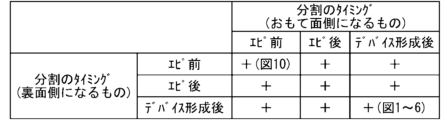
- 4A to 4C are diagrams showing patterns of wafer division timing in the semiconductor device manufacturing method according to the first embodiment;
- 1A to 1C are diagrams showing a basic process for dividing a SiC wafer before forming an epitaxial film in a manufacturing method for a semiconductor device according to a first embodiment.
- 11A to 11C are diagrams illustrating basic processes of a manufacturing method for a semiconductor device according to a second embodiment.
- 13A to 13C are diagrams illustrating basic processes of a semiconductor device manufacturing method according to a modified example of the second embodiment.
- 11A to 11C are diagrams illustrating basic processes of a manufacturing method for a semiconductor device according to a third embodiment.
- 13A to 13C are diagrams illustrating basic processes of a semiconductor device manufacturing method according to a modified example of the third embodiment.
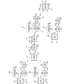
- Fig. 1 is a schematic diagram showing a basic process of the method for manufacturing a semiconductor device according to the present embodiment.
- Fig. 2 is a flow chart of the method for manufacturing a semiconductor device according to the present embodiment.
- the method for manufacturing a semiconductor device according to the present embodiment will be described with reference to Figs. 1 and 2.
- an epitaxial film 11 is formed on a single crystal SiC wafer 10, and a device surface structure (hereinafter, device structure) 12 is formed on the epitaxial film 11.
- the formation of the device structure 12 includes ion implantation and the formation of a surface electrode.
- the device structure 12 is, for example, a SiC power device structure.
- the device structure 12 is, for example, a GaN high frequency device structure, a GaN power device structure, or a gallium oxide power device structure.
- a GaN high frequency device structure, a GaN power device structure, or a gallium oxide power device structure may be formed on a SiC wafer.
- the SiC wafer 10 on which the epitaxial film 11 and the device structure 12 are formed is referred to as a SiC wafer 13.
- a SiC wafer 17 similar to the SiC wafer 13 is formed. That is, an epitaxial film 15 is formed on a single crystal SiC wafer 14, and a device structure 16 is formed on the epitaxial film 15.
- the SiC wafer 14 on which the epitaxial film 15 and the device structure 16 are formed is referred to as a SiC wafer 17.
- the SiC wafers 13 and 17 are also referred to as first wafers.
- the SiC wafers 10 and 14 may be bonded wafers formed by bonding multiple SiC wafers.
- the SiC wafers 10 and 14 have an N-type or P-type conductivity, or are semi-insulating.
- the SiC wafer 13 is divided into a device-attached wafer 19 including the device structure 12 and a divided wafer 20 not including the device structure 12.
- the device-attached wafer 19 includes a SiC wafer 18 separated from the SiC wafer 10, an epitaxial film 11 on the SiC wafer 18, and a device structure 12 on the epitaxial film 11.
- SiC wafer 17 is divided in the same manner as SiC wafer 13. That is, SiC wafer 17 is divided into device-attached wafer 22 including device structure 16 and split wafer 23 not including device structure 16.
- Device-attached wafer 22 comprises SiC wafer 21 separated from SiC wafer 14, epitaxial film 15 on SiC wafer 21, and device structure 16 on epitaxial film 15.
- Device-attached wafers 19 and 22 are also referred to as first device-attached wafers, and split wafers 20 and 23 are also referred to as first split wafers. Note that laser slicing technology or the like is used to divide SiC wafers 13 and 17 in this step.
- step S103 the backside of the device-attached wafers 19, 22, which is the side opposite the device structures 12, 16, is processed.
- the damaged layer on the backside of the device-attached wafers 19, 22 that has been damaged by laser slicing is removed by grinding or polishing, etc., and the device-attached wafers 19, 22 are adjusted to the desired thickness.
- normal backside processes such as the formation of backside electrodes (not shown) are performed on the backside of the device-attached wafers 19, 22.
- step S104 the front surfaces of the split wafers 20 and 23 are processed. Since the split wafers 20 and 23 also contain a damaged layer caused by laser slicing, this damaged layer is removed by grinding or polishing, and the split wafers 20 and 23 are adjusted to the desired thickness. Considering the depth of the bonding surface in the bonded wafer described later, the thickness of the split wafers 20 and 23 is preferably 50 ⁇ m or more, more preferably 80 ⁇ m or more, and most preferably 100 ⁇ m or more. When adjusting the thickness of the split wafers 20 and 23, the back side of the split wafers 20 and 23 may be processed, for example, by grinding or polishing, as necessary.
- a high-quality bonded wafer can be obtained in the subsequent step S105.
- a high-quality bonded wafer refers to one in which damage is suppressed, warping is suppressed, or flatness is improved.
- Processing the backside of the split wafers 20 and 23 can also be said to be a process that has a certain effect on producing wafers with devices by splitting and bonding.
- step S105 the divided wafers 20 and 23 are bonded.
- the wafer obtained by bonding the divided wafers 20 and 23 is called the bonded wafer 24.
- the bonded wafer 24 is also called the first bonded wafer.
- the bonded surfaces of the divided wafers 20 and 23 may be subjected to surface processing such as grinding, polishing, or CMP.
- the warpage or surface condition of the divided wafers 20 and 23 may be inspected, and the combination of the divided wafers 20 and 23 to be bonded may be determined according to the results. In this way, a high-quality bonded wafer is obtained.
- the two divided wafers 20 and 23 may be manufactured simultaneously or separately.
- the two divided wafers 20 and 23 may be manufactured simultaneously or sequentially using, for example, different processing equipment, or may be manufactured sequentially using the same processing equipment. In this way, flexible production is possible, and the productivity of the divided wafers can be improved. Note that, although two divided wafers 20 and 23 are described here as being bonded together, any number of divided wafers (three or more) may be bonded together to form the bonded wafer 24.
- the split wafers 20, 23 are bonded, for example, by room temperature bonding. Room temperature bonding results in a clean interface without the inclusion of a metal layer at the bonded interface. Furthermore, room temperature bonding results in an amorphous layer at the bonded interface.
- the bonded wafer 24 may be processed to the desired thickness by grinding, polishing, CMP, or the like. In this process, the bonded wafer 24 has a thickness similar to that of a normally used SiC wafer, making it possible to reuse the split wafers 20, 23 at lower cost and without the risk of cracking, compared to the case where a thick epitaxial film is formed on a thin SiC wafer to maintain the overall strength.
- the divided wafers 20 and 23 may be beveled to remove the sharp portions at the intersections of the outer circumferential surfaces and the cut surfaces, in other words, the corners of the divided wafers 20 and 23.
- the shape of the end of the bonded wafer 24 is a shape like the number "3" in cross section, or a broken line shape with five to seven mutation points. If the shape of the ends of the divided wafers 20 and 23 is curved, the shape of the end of the bonded wafer 24 becomes a shape like the number "3" after bonding.
- the shape of the ends of the divided wafers 20 and 23 is triangular, one mutation point is overlapped by bonding, and the shape of the end of the bonded wafer 24 becomes a broken line shape with five mutation points. If the shape of the ends of the divided wafers 20 and 23 is trapezoidal, one mutation point is overlapped by bonding, and the shape of the end of the bonded wafer 24 becomes a broken line shape with seven mutation points. In this case, beveling after bonding is not necessary, and the amount of cutting is small, so the area of the bonded wafer 24 can be increased.
- bevel processing may be performed on the bonded wafer 24 without performing bevel processing on the divided wafers 20, 23 before bonding.
- the bevel shape of the bonded wafer will be a curved shape like ")" or a trapezoidal shape in cross section, similar to a normal wafer that is not a bonded wafer.
- the effect of preventing chipping of the bonded wafer 24 is enhanced compared to a shape like "3".
- bevel processing may be performed on both the divided wafers 20, 23 before bonding and the bonded wafer 24 after bonding. In this case, it is possible to obtain both the effect of preventing chipping during processing and the effect of preventing chipping of the bonded wafer 24.
- step S106 an epitaxial film 25 is formed on the bonded wafer 24, and a device structure 26 is formed on the epitaxial film 25.
- the wafer thus formed is referred to as a bonded wafer 27.
- step S107 the bonded wafer 27 is divided in the thickness direction to obtain a device-equipped wafer 29 including the device structure 26 and a divided wafer 30 not including the device structure 26.
- the device-equipped wafer 29 is also referred to as a second device-equipped wafer, and the divided wafer 30 is also referred to as a second divided wafer.
- the device-equipped wafer 29 has a structure in which an epitaxial film 25 is formed on a SiC wafer 10, and a device structure 26 is formed on the epitaxial film 25. This process is similar to step S102.
- the bonded wafer 27 includes the bonding surfaces of the two divided wafers 20, 23, it is preferable that this bonding surface is not included in the device-attached wafer 29. This makes it possible to avoid variations in device characteristics due to the bonding surface in the device-attached wafer 29.
- the bonded wafer 27 is formed by room temperature bonding, an amorphous layer will be generated at the bonding interface, so it can be said that it is preferable that the SiC wafer 28 of the device-attached wafer 29 does not include an amorphous layer.
- the device-attached wafer 29 includes the bonding surfaces of the two divided wafers 20, 23, this may not be a problem, taking into consideration the type of device structure or the characteristics required for the device. In this case, it is not necessary to avoid including the bonding surface when obtaining the device-attached wafer 29, and the degree of freedom in process adjustment or thickness adjustment in the wafer division process can be improved.
- the device-equipped wafer 29 obtained in step S107 is again subjected to backside processing (not shown) in step S103.
- the divided wafer 30 obtained in step S107 may be again subjected to processing from step S104 onwards.
- the divided wafer 30 can then be bonded with another divided wafer to be used to create a further wafer with devices. That is, the processing from step S105 to step S107 is repeated at least once with the divided wafer 30, which is the second divided wafer, as the new first divided wafer.
- the amount of various defects such as crystal defects, for example, threading dislocations
- the crystal defect density on the surface layer of the bonded wafer on the side where the device structure is formed and the opposite side may differ, or the crystal defect density near the bonded interface may differ.
- threading dislocations that are continuous from the front to back surface of a normal wafer become discontinuous at the bonded interface of a bonded wafer.
- the amount of various defects differs between multiple split wafers, the effect of this on the device process or device characteristics can be ignored.
- the effect of the above-mentioned defect discontinuity on the device process or device characteristics can be further suppressed. Furthermore, if the bonded surface is not included in the wafer with devices, the effect of the above-mentioned defect discontinuity on the device characteristics can be eliminated.
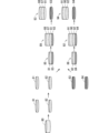
- Figures 3 to 6 are diagrams showing a flow when the basic process shown in Figure 1 is applied to actual operation.
- Figures 3 and 4 show an example of a flow for a SiC wafer having a thickness of 500 ⁇ m
- Figures 5 and 6 show an example of a flow for a SiC wafer having a thickness of 350 ⁇ m.
- FIGS. 3 and 5 show the process starting from SiC wafers A3 and B3 until bonded wafer E1 is formed.
- FIGS. 4 and 6 show the process until bonded wafer G1 is formed from bonded wafer E1 and SiC wafer F3.
- the numbers shown in the wafers indicate the thickness ( ⁇ m) of the wafers.
- the numbers in parentheses above or below the wafers indicate the thickness ( ⁇ m) of the removed wafers.
- the dashed lines in the wafers indicate the bonding surfaces, and the numbers in brackets next to the bonding surfaces indicate the depth ( ⁇ m) of the bonding surfaces, i.e., the depth ( ⁇ m) from the front surface of the bonded wafers to the bonding surfaces.
- the thickness and depth of each layer shown in these figures are examples and can be changed as appropriate.
- SiC wafers A3 and B3 are prepared.
- the thickness of SiC wafers A3 and B3, including the epitaxial film, is 510 ⁇ m.
- SiC wafer A3 is a SiC wafer A1 having device structure A2 formed on its front surface.
- SiC wafer B3 is a SiC wafer B1 having device structure B2 formed on its front surface.
- the device structure is assumed to include the epitaxial film.
- device structure A2 more specifically, includes an epitaxial film formed on SiC wafer A1 and a device structure formed on the epitaxial film. This is also true for other device structures that appear in the explanations of FIG. 3 to FIG. 6.
- SiC wafer A3 is split into device-attached wafer A4, which has device structure A2, and split wafer A12, which does not have device structure A2.
- Device-attached wafer A4 is composed of SiC wafer A11 and device structure A2 thereon. 50 ⁇ m is removed from the back surface of SiC wafer A11, leaving the thickness of SiC wafer A11 at 100 ⁇ m.
- Split wafer A12 has 50 ⁇ m removed from the front surface and 10 ⁇ m removed from the back surface, leaving a thickness of 300 ⁇ m.
- split wafer A12 is further removed by 25 ⁇ m, leaving a thickness of 275 ⁇ m.
- SiC wafer B3 is split into device-attached wafer B4, which has device structure B2, and split wafer B12, which does not have device structure B2.
- Device-attached wafer B4 is composed of SiC wafer B11 and device structure B2 thereon.
- SiC wafer B11 has 50 ⁇ m removed from the back surface, leaving it with a thickness of 100 ⁇ m.
- Split wafer B12 has 50 ⁇ m removed from the front surface and 10 ⁇ m removed from the back surface, leaving it with a thickness of 300 ⁇ m.
- split wafer B12 is further removed by 25 ⁇ m, leaving a thickness of 275 ⁇ m.
- the split wafers A12 and B12 are bonded together to obtain a bonded wafer C1 with a thickness of 550 ⁇ m.
- the depth of the bonded surface of the bonded wafer C1 is 275 ⁇ m.
- the front surface of the bonded wafer C1 is removed by a thickness of 50 ⁇ m, so that the thickness of the bonded wafer C1 is 500 ⁇ m.
- the depth of the bonded surface of the bonded wafer C1 is 225 ⁇ m.
- the device structure C2 is formed on the bonded wafer C1.
- the wafer consisting of the bonded wafer C1 and the device structure C2 is called the bonded wafer C3.
- the thickness of the bonded wafer C3 is 510 ⁇ m, and the depth of the bonded surface in the bonded wafer C3 is 235 ⁇ m.
- the bonded wafer C3 is divided into a device-attached wafer C4 having the device structure C2 and a divided wafer C5 not having the device structure C2.
- the device-attached wafer C4 is composed of a SiC wafer A121, which is a part of the divided wafer A12, and the device structure C2 on the SiC wafer A121.
- the bonding surface of the bonded wafer C3 is not included in the device-attached wafer C4.
- the back surface of the SiC wafer A121 is removed by 50 ⁇ m, so that the thickness of the device-attached wafer C4 becomes 100 ⁇ m.
- the divided wafer C5 is composed of a SiC wafer A122, which is a part of the divided wafer A12, and a divided wafer B12.
- the front surface of the divided wafer C5 is removed by 50 ⁇ m, and the back surface is removed by 10 ⁇ m, so that the thickness of the divided wafer C5 becomes 300 ⁇ m.
- the depth of the bonding surface of the divided wafer C5 is 35 ⁇ m.
- split wafer C5 is further removed by 25 ⁇ m, leaving a thickness of 275 ⁇ m.
- SiC wafer D3 is prepared.
- SiC wafer D3 is a SiC wafer D1 with device structure D2 formed on the front surface.
- SiC wafer D3 is split into device-attached wafer D4, which has device structure D2, and split wafer D12, which does not have device structure D2.
- Device-attached wafer D4 is composed of SiC wafer D11 and device structure D2 thereon. 50 ⁇ m is removed from the back surface of SiC wafer D11, making the thickness of SiC wafer D11 100 ⁇ m.
- Split wafer D12 has 50 ⁇ m removed from the front surface and 10 ⁇ m removed from the back surface, making the thickness 300 ⁇ m.
- split wafer D12 is further removed by 25 ⁇ m, leaving a thickness of 275 ⁇ m.
- bonded wafer E1 includes a first bonding surface which is the bonding surface between SiC wafer A122 and split wafer B12, and a second bonding surface which is the bonding surface between split wafer B12 and split wafer D12.
- the depth of the first bonding surface is 35 ⁇ m, and the depth of the second bonding surface is 275 ⁇ m.
- the SiC wafer A122 is removed from the bonded wafer E1, and the thickness of the bonded wafer E1 becomes 500 ⁇ m.
- the depth of the bonded surface in the bonded wafer E1 is 225 ⁇ m.
- a device structure E2 is formed on the front surface of the bonded wafer E1.
- the SiC wafer consisting of the bonded wafer E1 and the device structure E2 thereon is referred to as bonded wafer E3.
- the thickness of the bonded wafer E3 is 510 ⁇ m, and the depth of the bonded surface in the bonded wafer E3 is 235 ⁇ m.
- the bonded wafer E3 is divided into a device-attached wafer E4 having the device structure E2, and a divided wafer E5 without the device structure E2.
- the device-attached wafer E4 is composed of a SiC wafer B121, which is part of the divided wafer B12, and the device structure E2 thereon.
- the divided wafer E5 is composed of a divided wafer D12 and a SiC wafer B122, which is part of the divided wafer B12. 50 ⁇ m is removed from the front surface of the divided wafer E5, and 10 ⁇ m is removed from the back surface, leaving a thickness of 300 ⁇ m.
- split wafer D12 is further removed by 25 ⁇ m, leaving a thickness of 275 ⁇ m.
- a SiC wafer F3 is prepared.
- the SiC wafer F3 is a SiC wafer F1 with a device structure F2 formed on the front surface.
- the SiC wafer F3 is divided into a device-attached wafer F4 having the device structure F2, and a divided wafer F12 without the device structure F2.
- the device-attached wafer F4 is composed of a SiC wafer F11 and a device structure F2 thereon. 50 ⁇ m is removed from the back surface of the SiC wafer F11, making the thickness of the SiC wafer F11 100 ⁇ m.
- the divided wafer F12 has 50 ⁇ m removed from the front surface and 10 ⁇ m removed from the back surface, making the thickness 300 ⁇ m.
- split wafer F12 is further removed by 25 ⁇ m, leaving a thickness of 275 ⁇ m.
- bonded wafer G1 includes a first bonding surface which is the bonding surface between SiC wafer B122 and split wafer D12, and a second bonding surface which is the bonding surface between split wafer D12 and split wafer F12.
- the depth of the first bonding surface is 35 ⁇ m, and the depth of the second bonding surface is 275 ⁇ m.
- the SiC wafer B122 is removed from the bonded wafer G1, and the thickness of the bonded wafer G1 becomes 500 ⁇ m.
- the depth of the bonded surface in the bonded wafer G1 is 225 ⁇ m.
- Three device-equipped wafers A4, B4, and C4 were obtained from two SiC wafers A3 and B3.
- Five device-equipped wafers A4, B4, C4, D4, and E4 were obtained from three SiC wafers A3, B3, and D3.
- (2n-1) device-equipped wafers can be obtained from n SiC wafers 10. This makes it possible to produce device-equipped wafers by reducing the number of SiC wafers used, resulting in cost reduction effects.
- SiC wafers A3, B3, D3, and F3 are described as having an epitaxial film of 10 ⁇ m formed on a 500 ⁇ m thick SiC wafer.
- the thickness of each layer constituting SiC wafers A3, B3, D3, and F3 is not limited to this and can be changed as appropriate depending on the desired device characteristics or wafer thickness.
- Figures 5 and 6 show a case where the wafer thickness is 350 ⁇ m and the epitaxial film thickness is 10 ⁇ m.
- the thickness of the device-attached wafers A4, C4, and E4 is 100 ⁇ m, but this is not limited and can be appropriately selected depending on the device characteristics. Also, 50 ⁇ m of the backside of the SiC wafers A11, A121, and B121 is removed, but this is not limited. In order to remove the damaged layer caused during division and to make the device-attached wafers A4, C4, and E4 have the desired thickness, the amount of removal of the backside of the SiC wafers A11, A121, and B121 can be appropriately selected, for example, between 10 ⁇ m and 100 ⁇ m.
- the thickness of the divided wafers A12, C5, and E5 is 275 ⁇ m, but this is not limited.
- the thickness of the divided wafers A12, C5, and E5 may be 50 ⁇ m or more, preferably 80 ⁇ m or more, and most preferably 100 ⁇ m or more. This prevents the divided wafers from cracking, and also enables operation of the device-attached wafers C4 and E4 without a bonding surface. By not having a bonding surface, the device-attached wafer eliminates the effect of the bonding surface on the device characteristics, and it is possible to obtain characteristics equivalent to those of devices made with normal wafers that do not use bonding means.
- the amount of removal from the front surfaces of the divided wafers A12, C5, and E5 may be appropriately selected, for example, between 10 ⁇ m and 100 ⁇ m.
- the processing of the backsides of the divided wafers A12, C5, and E5 is performed in two separate steps, but this is not limited to this and the processing may be performed all at once or in multiple steps of two or more steps. If it is performed all at once, the number of steps can be reduced. If it is divided into multiple steps, improvement in quality after removal can be expected.
- each of the divided wafers A12, C5, and E5 is removed by a total of 35 ⁇ m in two steps.
- the amount of removal of the rear surface of the divided wafers A12, C5, and E5 is not limited to this, and can be selected appropriately so that the divided wafers A12, C5, and E5 have the desired thickness. Also, if the divided wafers A12, C5, and E5 can be made to the desired thickness by processing the front surface, it is not necessary to process the rear surface.
- the laser marking that is usually applied to the wafer can be removed, so that the effect of the laser marking during bonding, that is, damage or unevenness on the bonding surface, can be eliminated, and the quality of the bonded wafer can be improved.
- This effect is seen when the total amount of removal of the rear surface of the divided wafers is 1 ⁇ m or more, and is particularly noticeable when it is 30 ⁇ m or more.
- the total removal amounts of the front surfaces of divided wafers A12, C5, E5 and divided wafers B12, D12, F12 are different, but they may be the same. If they are the same, the processing processes for these divided wafers can be unified, which is advantageous in terms of productivity. Also, in the examples of Figures 3 and 4, the total removal amounts of the back surfaces of divided wafers A12, C5, E5 and divided wafers B12, D12, F12 are different, but they may be the same. If they are the same, the processing processes for these divided wafers can be unified, which is advantageous in terms of productivity.
- split wafers each having a thickness of 275 ⁇ m are bonded together to produce bonded wafers C1, E1, and G1 each having a thickness of 550 ⁇ m.
- the thickness of the split wafers is not limited to this and can be changed as appropriate.
- Split wafers of different thicknesses may also be bonded together; for example, split wafer A12 and split wafer B12 may have different thicknesses.
- the amount of removal from the front surface of the bonded wafers C1, E1, and G1 is not limited to this, and can be changed as appropriate so that the bonded wafers C1, E1, and G1 have the desired thickness. Also, if the desired thickness is achieved at the time of bonding, removal here is not necessary.
- the film thickness of the bonded wafer does not need to be the same as that of the original wafers, and may be different. If the wafer after bonding is thicker, cracks and warping can be further reduced in the device manufacturing process. If they are the same, the same process as for normal wafers is possible. Even if it is thin, if the thickness of the bonded wafer is 100 ⁇ m or more, more preferably 250 ⁇ m, and most preferably 300 ⁇ m or more, it is easy to flow the device process.
- finishing processing may be performed by grinding, polishing, CMP, etc.
- precise processing may be required to reduce surface roughness, and it is desirable to perform mirror finishing by polishing or CMP. This allows the production of high-quality bonded wafers.
- the device structures A2, B2, C2, D2, E2, and F2 illustrated in Figures 3 and 4 may be the same structure or different.
- the device structure on the normal wafer and the device structure on the bonded wafer may be different.
- device structure A2 and device structure C2 may be different.
- the bonded wafer is thin and therefore more sensitive to warping or cracking than a normal wafer, warping or cracking can be avoided by manufacturing a device with a small process load on the bonded wafer.
- the effects of warping or cracking of the bonded wafer can be reduced by manufacturing a device that requires a thick epitaxial film.
- the device structure referred to here may be one in which semiconductor elements such as diodes, transistors, and thyristors, or a combination of these, are formed.
- the device structure on the bonded wafer may be determined based on the manufacturing yield of devices fabricated from normal wafers. In other words, if the quality of normal wafers is low and the manufacturing yield of devices fabricated using them is low, a device structure that is insensitive to the quality of the wafer may be formed on the bonded wafer obtained by dividing and bonding the wafer. If the quality of normal wafers is high and the manufacturing yield of devices fabricated using them is high, a device structure that is sensitive to the quality of the wafer may be formed on the bonded wafer obtained by dividing and bonding the wafer.
- the quality of the wafer may be determined by the amount or type of defects that affect the device characteristics.
- the device manufacturing yield not only the device manufacturing yield but also at least one of the amount and type of defects may be measured before the device structure is fabricated, and the device structure on the bonded wafer may be determined after obtaining information that determines whether the desired characteristics are obtained.
- the manufacturing yield of the entire factory can be improved.
- Wafer thickness and bonding surface depth may affect the characteristics of the device. In particular, if a bonding defect occurs at the bonding surface, the device characteristics are adversely affected. In order to avoid such a risk, it is preferable that the device-attached wafer 29 is formed by avoiding the bonding surface of the bonded wafer. Therefore, it is preferable that the depth of the bonding surface in the bonded wafer 24 is greater than the thickness of the device-attached wafer 29.
- the depth of the bonding surface in the bonded wafer 24 is preferably 50 ⁇ m or more, more preferably 80 ⁇ m or more, and most preferably 100 ⁇ m or more.
- the depth of the bonded surface is 225 ⁇ m. In the bonded wafers C1, E1, and G1 before the device structure is formed as shown in Figures 5 and 6, the depth of the bonded surface is 160 ⁇ m.
- the depth of the bonded surface is 50 ⁇ m or more from the surface of the bonded wafer. Also, as shown in Figure 8, when the bonded wafer is made by bonding three divided wafers together, it is desirable that the depth of the shallowest bonded surface is 50 ⁇ m or more from the surface of the bonded wafer.
- the thickness of the bonded wafers C1, E1, and G1 is 500 ⁇ m, and in Figures 5 and 6, the thickness of the bonded wafers C1, E1, and G1 is 350 ⁇ m.
- the thickness of these bonded wafers is determined taking into consideration the fact that no warping occurs when a device structure is formed on the bonded wafer.
- the thickness of the bonded wafer is preferably 100 ⁇ m or more, more preferably 250 ⁇ m, and most preferably 300 ⁇ m or more.
- Wafer division timing> In FIG. 1 to FIG. 6, the split wafers were split from the SiC wafer having the device structure. That is, the split was performed after the device structure was formed on the SiC wafer.
- the timing at which the split wafers constituting the bonded wafer are split from the original SiC wafer is not limited to after the device structure was formed on the original SiC wafer.
- the split timing of various wafers is indicated by "+".
- Both the split wafer that will become the front side of the bonded wafer by later bonding and the split wafer that will become the back side may be split before an epitaxial film is formed on the original SiC wafer (pre-epi), may be split before the device structure is formed on the original SiC wafer after the epitaxial film is formed on the original SiC wafer (post-epi), or may be split after the device structure is formed on the original SiC wafer.
- the split wafer that will become the front side of the bonded wafer by later bonding and the split wafer that will become the back side may be split from the original SiC wafer at different timings. In other words, the split process may be performed before the epitaxial film is formed, before the device is formed, or after the device is formed.
- Figure 10 shows the basic process for dividing a SiC wafer before forming an epitaxial film. Below, the basic process is explained with reference to Figure 10.
- a high-quality SiC wafer 40 and a low-quality SiC wafer 43 are prepared.
- the difference in quality between the two SiC wafers 40, 43 is manifested, for example, in the number of defects or flatness.
- the high-quality SiC wafer 40 has a smaller surface defect density or dislocation density in the crystal than the low-quality SiC wafer 43.
- the quality of the SiC wafer can be determined, for example, by optical microscope observation, photoluminescence imaging observation, or X-ray diffraction analysis.
- SiC wafer 40 is divided into two high-quality split wafers 41 and 42, and similarly SiC wafer 43 is divided into two low-quality split wafers 44 and 45. Damage layers formed on the cut surfaces of split wafers 41, 42, 44, and 45 are then removed by grinding or polishing.
- the high-quality divided wafer 41 and the low-quality divided wafer 44 are bonded together to form a bonded wafer 46. Furthermore, the high-quality divided wafer 42 and the low-quality divided wafer 45 are bonded together to form a bonded wafer 47.
- an epitaxial film 48 and a device structure 49 are formed on the bonded wafer 46.
- the wafer consisting of the bonded wafer 46, the epitaxial film 48, and the device structure 49 is referred to as a bonded wafer 50.
- an epitaxial film 51 and a device structure 52 are formed on the bonded wafer 47.
- the wafer consisting of the bonded wafer 47, the epitaxial film 51, and the device structure 52 is referred to as a bonded wafer 53.
- the bonded wafer 50 is divided into a device-attached wafer 54 having a device structure 49 and a split wafer 44.
- the device-attached wafer 54 is composed of a high-quality split wafer 41, an epitaxial film 48, and a device structure 49.
- the bonded wafer 53 is divided into a device-attached wafer 55 having a device structure 52 and a split wafer 45.
- the device-attached wafer 55 is composed of a high-quality split wafer 42, an epitaxial film 51, and a device structure 52.
- a low-quality SiC wafer is used as the backside wafer of the bonded wafer, i.e., as the support substrate, and multiple wafers with devices are created from a high-quality SiC wafer. Also, by dividing multiple wafers from the initial SiC wafer before the formation of the epitaxial film, all of the divided divided wafers can be reused. Note that using a high-quality divided wafer as the front side of the bonded wafer and a low-quality wafer as the back side of the bonded wafer can also be applied to the case where the wafer is divided after device formation as described in Figures 1 to 6. Assessing the quality of the wafer and using a high-quality divided wafer as the front side of the bonded wafer as in this method allows the high-quality wafer to be used more efficiently, making it possible to improve the overall device yield of the manufacturing plant and further improving productivity.
- the original wafer is a single crystal SiC wafer.
- SiC is easy to process, so there is an advantage that the divided wafers can be easily bonded together.
- the original wafer for example, the first wafer, the first divided wafer, or the first bonded wafer, is not limited to SiC, and may be made of other single crystal materials such as diamond, gallium nitride (GaN), gallium oxide (Ga2O3), and aluminum nitride (AlN). Even in such a case, there is no difference in the thermal expansion coefficient between the divided wafers, so that stable bonding can be performed.
- each divided wafer that constitutes the bonded wafer is the same.
- the thickness of divided wafers A12 and B12 that constitute bonded wafer C1 is both 275 ⁇ m.
- the thickness of divided wafers A12 and B12 that constitute bonded wafer C1 is both 190 ⁇ m.
- the thickness of each divided wafer that constitutes the bonded wafer does not have to be the same.
- one bonded wafer is divided into one wafer with a device and one divided wafer without a device structure.
- one bonded wafer may be divided into one wafer with a device and multiple divided wafers without a device structure.
- one SiC wafer 40 is divided into two divided wafers 41 and 42. However, one SiC wafer 40 may be divided into multiple divided wafers. This also applies to SiC wafer 43 in the example of FIG. 10.
- the method for manufacturing a semiconductor device includes the steps of (a) obtaining at least one divided wafer 20, 23 not including a device structure from each of the SiC wafers 13, 17 by dividing each of the multiple SiC wafers 13, 17 in the thickness direction, (b) obtaining a bonded wafer 24 by bonding the multiple divided wafers 20, 23 obtained from different SiC wafers 13, 17, and (c) forming a device structure 26 on the surface of the bonded wafer 24.
- the remaining divided wafers 20 from which the device-equipped wafer 19 has been obtained from the SiC wafer 13 can be reused together with other divided wafers 23 to obtain a further device-equipped wafer 29.
- the method described in Patent Document 1 in which a thick epitaxial layer is formed on a split wafer, is not economical and has the problem that the wafer is prone to warping and cracking.
- the method of the present embodiment bonds the split wafers together, making it possible to reuse the wafers at low cost while suppressing warping.
- the bonded wafer 24 is a bonded wafer formed by bonding together a number of split wafers 20, 23 that do not include device structures and that have been separated from different SiC wafers 13, 17.
- the bonded surfaces of the multiple split wafers 20, 23 are located at a depth of 50 ⁇ m or more from the surface of the bonded wafer 24. This makes it possible to manufacture a device-equipped wafer 29 that does not include a bonded surface using the bonded wafer 24. This makes it possible to avoid the effect of the bonded surfaces on the characteristics of the devices.
- a bonded wafer is formed by bonding a plurality of divided wafers together.
- a bonded wafer is formed by bonding one divided wafer to a single crystal wafer that is not a divided wafer.
- Basic process> 11 is a schematic diagram showing a basic process in the method for manufacturing a semiconductor device in the embodiment 2.
- the method for manufacturing a semiconductor device in the embodiment 2 will be described with reference to FIG.
- a SiC wafer 63 and a single crystal SiC wafer 67 are prepared.
- the SiC wafer 63 is formed by forming an epitaxial film 61 on a SiC wafer 60, and further forming a device structure 62 on the epitaxial film 61.
- the SiC wafer 63 is divided into a device-attached wafer 65 having the device structure 62 and a divided wafer 66 not having the device structure 62.
- the device-attached wafer 65 is composed of a SiC wafer 64 separated from the SiC wafer 60, an epitaxial film 61 on the SiC wafer 64, and a device structure 62 on the epitaxial film 61.
- the back surface of the device-mounted wafer 65 and the front surface of the split wafer 66 have layers of damage caused by splitting. These layers of damage are removed by grinding or polishing, etc.
- the split wafer 66 is then bonded to the single crystal SiC wafer 67, thus forming a bonded wafer 68.
- the split wafer 66 is the front side of the bonded wafer 68, and the single crystal SiC wafer 67 is the back side of the bonded wafer 68. In this way, the single crystal SiC wafer 67 is used as a support substrate for the split wafer 66.
- an epitaxial film 69 is formed on the bonded wafer 68, and a device structure 70 is further formed on the epitaxial film 69.
- the wafer consisting of the bonded wafer 68, the epitaxial film 69, and the device structure 70 is called a bonded wafer 71.
- the bonded wafer 71 is divided into a device-attached wafer 72 having a device structure 70 and a single crystal SiC wafer 67.
- the device-attached wafer 72 does not include a bonding surface between the split wafer 66 and the single crystal SiC wafer 67. Therefore, taking into consideration the thickness of the device structure 70, the bonding surface between the split wafer 66 and the single crystal SiC wafer 67 in the bonded wafer 68 is preferably located at a depth of 50 ⁇ m or more from the surface of the bonded wafer 68, more preferably at a depth of 80 ⁇ m, and most preferably at a depth of 100 ⁇ m or more.
- the thickness of the split wafer 66 is preferably 50 ⁇ m or more, more preferably at a depth of 80 ⁇ m or more, and most preferably at a depth of 100 ⁇ m or more.
- the device-attached wafer 72 does not include a bonding surface, and the influence of the bonding surface on the device can be eliminated.
- the single crystal SiC wafer 67 is used as a support substrate when forming the device structure 70 on the split wafer 66. After being split from the bonded wafer 71, the single crystal SiC wafer 67 can be reused as a support substrate for another split wafer.
- the support substrate may not have a structure such as warping, surface roughness, or surface irregularities suitable for bonding with the SiC wafer.
- the surface of the SiC wafer to be bonded to the support substrate may be ground, polished, or treated with CMP, or the SiC wafer may be treated with pressure or heat, so that a structure such as warping, surface roughness, or surface irregularities suitable for bonding with the support substrate may be formed on the SiC wafer or the support substrate, or on both. This allows for good bonding between the SiC wafer and the support substrate.
- the thickness of the single crystal SiC wafer 67 separated from the bonded wafer 71 may vary from the thickness of the original single crystal SiC wafer 67. In other words, when separating the single crystal SiC wafer 67 from the bonded wafer 71, it is not necessary to separate the single crystal SiC wafer 67 at the bonding surface between the separated wafer 66 and the single crystal SiC wafer 67.
- the bonding surface may be removed by removing a damaged layer of the single crystal SiC wafer 67 after separation. The bonding surface may remain on the single crystal SiC wafer 67 after separation.
- one SiC wafer 63 is divided into one wafer 65 with devices and one divided wafer 66 without a device structure.
- one SiC wafer 63 may be divided into one wafer 65 with devices and multiple divided wafers without a device structure.
- a single crystal GaN wafer or a single crystal gallium oxide wafer may be used instead of the single crystal SiC wafer 67.
- Such alternative wafers may be used from the viewpoint of heat management in the device manufacturing process, such as heat dissipation from the wafer or heat storage in the wafer.
- a wafer made of another material mentioned in the first embodiment may be used. In that case, if the wafer used as the support substrate and the divided wafers are made of the same material, it is easier to ensure the bonding strength.
- the amount of various defects such as crystal defects, for example, threading dislocations
- the crystal defect density on the surface layer of the bonded wafer on the side where the device structure is formed and the opposite side may differ, or the crystal defect density near the bonded interface may differ.
- threading dislocations that are continuous from the front to back surface of a normal wafer become discontinuous at the bonded interface of a bonded wafer.
- the amount of various defects differs between multiple wafers, the effect of this on the device process or device characteristics can be ignored.
- the effect of the discontinuity of the above-mentioned defects on the device process or device characteristics can be further suppressed. Furthermore, if the bonded surface is not included in the wafer with devices, the effect of the discontinuity of the above-mentioned defects on the device characteristics can be eliminated.
- Modified Examples> 12 is a schematic diagram showing a basic process in a method for manufacturing a semiconductor device according to a modification of the second embodiment. In this modification, the SiC wafer is divided before the epitaxial film is formed.
- the method for manufacturing a semiconductor device according to the modification of the second embodiment will be described with reference to FIG.
- a SiC wafer 80 and two single crystal SiC wafers 83 and 84 are prepared.
- the SiC wafer 80 is divided into two split wafers 81 and 82.
- split wafer 81 and the front surface of split wafer 82 have layers damaged by splitting. These layers are removed by grinding or polishing, etc.
- the split wafer 81 and the single crystal SiC wafer 83 are bonded to form a bonded wafer 85, and the split wafer 82 and the single crystal SiC wafer 84 are bonded to form a bonded wafer 86.
- the single crystal SiC wafers 83 and 84 are used as support substrates for the split wafers 81 and 82.
- an epitaxial film 87 is formed on the bonded wafer 85, and a device structure 88 is formed on the epitaxial film 87.
- the wafer consisting of the bonded wafer 85, the epitaxial film 87, and the device structure 88 is referred to as a bonded wafer 89.
- an epitaxial film 90 is formed on the bonded wafer 86, and a device structure 91 is formed on the epitaxial film 90.
- the wafer consisting of the bonded wafer 86, the epitaxial film 90, and the device structure 91 is referred to as a bonded wafer 92.
- the bonded wafer 89 is divided into a device-attached wafer 93 having a device structure 88 and a single crystal SiC wafer 83.
- the device-attached wafer 93 comprises a split wafer 81, an epitaxial film 87, and a device structure 88.
- the bonded wafer 92 is divided into a device-attached wafer 94 having a device structure 91 and a single crystal SiC wafer 84.
- the device-attached wafer 94 comprises a split wafer 82, an epitaxial film 90, and a device structure 91.
- the device-attached wafers 93, 94 do not include the bonding surfaces between the divided wafers 81, 82 and the single crystal SiC wafers 83, 84. Therefore, taking into consideration the thickness of the device structures 88, 91, the bonding surfaces between the divided wafers 81, 82 and the single crystal SiC wafers 83, 84 in the bonded wafers 85, 86 are preferably located at a depth of 50 ⁇ m or more, more preferably 80 ⁇ m or more, and most preferably 100 ⁇ m or more from the surface of the bonded wafers 85, 86.
- the thickness of the divided wafers 81, 82 is preferably 50 ⁇ m or more, more preferably 80 ⁇ m or more, and most preferably 100 ⁇ m or more.
- the device-attached wafers 93, 94 do not include the bonding surfaces, and the influence of the bonding surfaces on the devices can be eliminated.
- the single crystal SiC wafers 83, 84 as a support substrate, it is possible to form device structures 88, 91 on multiple divided wafers 81, 82 separated from the SiC wafer.
- the single crystal SiC wafers 83, 84 separated from the bonded wafers 89, 92 can be reused as support substrates for other divided wafers.
- the thickness of the single crystal SiC wafers 83, 84 separated from the bonded wafers 89, 92 may vary from the thickness of the original single crystal SiC wafers 83, 84.
- the bonding surfaces may be removed by removing the damaged layers of the single crystal SiC wafers 83, 84 after separation. The bonding surfaces may remain on the single crystal SiC wafers 83, 84 after separation.
- one SiC wafer 80 is divided into two divided wafers 81 and 82.
- one SiC wafer 80 may be divided into three or more divided wafers.
- a wafer of another material mentioned in the first embodiment may be used.
- the wafer used as the support substrate and the divided wafers are made of the same material to ensure the bonding strength.
- the method for manufacturing a semiconductor device includes the steps of (a) dividing a wafer in the thickness direction to obtain divided wafers, (b) bonding the divided wafers to a single crystal support substrate to obtain a bonded wafer, and (c) forming a device structure on the bonded wafer. This makes it possible to manufacture semiconductor devices by reusing the wafer with high productivity while suppressing cracking of the wafer.
- the bonded wafer according to the second embodiment is a bonded wafer formed by bonding a divided wafer that does not include a device structure separated from a wafer to a support substrate, and it is desirable that the bonding surface between the divided wafer and the support substrate is located at a depth of 50 ⁇ m or more from the surface.
- the wafer with the device structure does not include the bonding surface, so that the effect of the bonding surface on the device can be eliminated.
- the wafer that will become the support substrate is manufactured by splitting it from a normal wafer, which may limit the thickness of the support substrate or result in waste when removing the support substrate or split wafer to obtain a bonded wafer with the desired film thickness.
- the support substrate is manufactured by splitting it directly from an ingot. Therefore, there is no limit to the thickness, and single crystal wafers with the required thickness for the support substrate can be directly manufactured, reducing waste. This makes it possible to achieve a high cost reduction effect.
- by using low-quality crystals with many crystal defects that are not suitable for device manufacturing as the support substrate it is also possible to reduce material loss throughout the entire manufacturing process.
- a bonded wafer is formed by bonding one divided wafer to a monocrystalline wafer that is not a divided wafer.
- a bonded wafer is formed by bonding one divided wafer to a polycrystalline wafer that is not a divided wafer.
- Basic process> 13 is a schematic diagram showing a basic process in the method for manufacturing a semiconductor device in the embodiment 3.
- the method for manufacturing a semiconductor device in the embodiment 3 will be described with reference to FIG.
- a SiC wafer 103 and a polycrystalline SiC wafer 107 are prepared.
- the SiC wafer 103 is formed by forming an epitaxial film 101 on a SiC wafer 100, and further forming a device structure 102 on the epitaxial film 101.
- the SiC wafer 103 is divided into a device-equipped wafer 105 having the device structure 102 and a divided wafer 106 not having the device structure 102.
- the device-equipped wafer 105 is composed of a SiC wafer 104 divided from the SiC wafer 100, an epitaxial film 101 on the SiC wafer 104, and a device structure 102 on the epitaxial film 101.
- the back surface of the device-mounted wafer 105 and the front surface of the split wafer 106 have layers of damage caused by splitting. These layers of damage are removed by grinding or polishing, etc.
- the split wafer 106 is bonded to the polycrystalline SiC wafer 107, thus forming the bonded wafer 108.
- the split wafer 106 is the front side of the bonded wafer 108, and the polycrystalline SiC wafer 107 is the back side of the bonded wafer 108.
- the polycrystalline SiC wafer 107 is used as a support substrate for the split wafer 106.
- an epitaxial film 109 is formed on the bonded wafer 108, and a device structure 110 is further formed on the epitaxial film 109.
- the wafer consisting of the bonded wafer 108, the epitaxial film 109, and the device structure 110 is called a bonded wafer 111.
- the bonded wafer 111 is divided into a device-attached wafer 112 having a device structure 110 and a polycrystalline SiC wafer 107.
- the polycrystalline SiC wafer 107 is used as a support substrate when forming the device structure 110 on the divided wafer 106.
- the polycrystalline SiC wafer 107 can be reused as a support substrate for another divided wafer.
- the support substrate may not have a structure such as warping, surface roughness, or surface irregularities suitable for bonding with a SiC wafer.
- the surface of the SiC wafer to be bonded to the support substrate may be ground, polished, or treated with CMP, or the SiC wafer may be treated with pressure or heat, so that a structure such as warping, surface roughness, or surface irregularities suitable for bonding with the support substrate may be formed on the SiC wafer or the support substrate, or both. This allows for good bonding between the SiC wafer and the support substrate.
- the thickness of the polycrystalline SiC wafer 107 separated from the bonded wafer 111 may vary from the thickness of the original polycrystalline SiC wafer 107. That is, when separating the polycrystalline SiC wafer 107 from the bonded wafer 111, the separation may occur at the bonding surface between the separated wafer 106 and the polycrystalline SiC wafer 107, but this is not necessary.
- the bonding surface may be removed by removing a damaged layer of the polycrystalline SiC wafer 107 after separation. The bonding surface may remain on the polycrystalline SiC wafer 107 after separation.
- the bonded wafer 108 includes the bonding surface between the divided wafer 106 and the polycrystalline SiC wafer 107. It is preferable that the device-attached wafer 112 does not include this bonding surface. Therefore, the depth of the bonding surface between the divided wafer 106 and the polycrystalline SiC wafer 107 in the bonded wafer 108 is preferably 50 ⁇ m or more, more preferably 80 ⁇ m or more, and most preferably 100 ⁇ m or more. In other words, the thickness of the divided wafer 106 separated from the SiC wafer 103 is preferably 50 ⁇ m or more, more preferably 80 ⁇ m or more, and most preferably 100 ⁇ m or more. This means that the device-attached wafer 112 does not include the bonding surface, and the effect of the bonding surface on the devices can be eliminated.
- one SiC wafer 103 is divided into one wafer 105 with devices and one divided wafer without a device structure.
- one SiC wafer 103 may be divided into one wafer 105 with devices and multiple divided wafers without a device structure.
- a wafer of another material mentioned in the first embodiment may be used.
- the wafer used as the support substrate and the divided wafers are made of the same material in order to ensure the bonding strength.
- the amount of various defects such as crystal defects, for example, threading dislocations
- the crystal defect density on the surface layer of the bonded wafer on the side where the device structure is formed and the opposite side may differ, or the crystal defect density near the bonded interface may differ.
- threading dislocations that are continuous from the front to back surface of a normal wafer become discontinuous at the bonded interface of a bonded wafer.
- the amount of various defects differs between multiple wafers, the effect of this on the device process or device characteristics can be ignored.
- the effect of the discontinuity of the above-mentioned defects on the device process or device characteristics can be further suppressed. Furthermore, if the bonded surface is not included in the wafer with devices, the effect of the discontinuity of the above-mentioned defects on the device characteristics can be eliminated.
- Modified Examples> 14 is a schematic diagram showing a basic process in a method for manufacturing a semiconductor device in a modified example of the third embodiment.
- the division of the SiC wafer is performed before the formation of the epitaxial film.
- the division of the SiC wafer may be performed after the formation of the epitaxial film and before the formation of the device structure.
- the method for manufacturing a semiconductor device in the modified example of the third embodiment will be described with reference to FIG. 14.
- a SiC wafer 120 and two polycrystalline SiC wafers 123 and 124 are prepared.
- the SiC wafer 120 is divided into two split wafers 121 and 122.
- split wafer 121 and the front surface of split wafer 122 have layers damaged by splitting. These layers are removed by grinding or polishing, etc.
- divided wafer 121 and polycrystalline SiC wafer 123 are bonded to form bonded wafer 125, and divided wafer 122 and polycrystalline SiC wafer 124 are bonded to form bonded wafer 126.
- polycrystalline SiC wafer 123 is used as a support substrate for divided wafer 121
- polycrystalline SiC wafer 124 is used as a support substrate for divided wafer 122.
- epitaxial film 127 is formed on bonded wafer 125, and device structure 128 is formed on epitaxial film 127.
- the wafer consisting of bonded wafer 125, epitaxial film 127, and device structure 128 is referred to as bonded wafer 129.
- epitaxial film 130 is formed on bonded wafer 126, and device structure 131 is formed on epitaxial film 130.
- the wafer consisting of bonded wafer 126, epitaxial film 130, and device structure 131 is referred to as bonded wafer 132.
- the bonded wafers 125, 126 include the bonding surfaces of the divided wafers 121, 122 and the polycrystalline SiC wafers 123, 124. It is preferable that the device-attached wafers 133, 134 do not include this bonding surface. Therefore, the depth of the bonding surface between the divided wafers 121, 122 and the polycrystalline SiC wafers 123, 124 in the bonded wafers 125, 126 is preferably 50 ⁇ m or more, more preferably 80 ⁇ m or more, and most preferably 100 ⁇ m or more.
- the thickness of the divided wafers 121, 122 separated from the SiC wafer 120 is preferably 50 ⁇ m or more, more preferably 80 ⁇ m or more, and most preferably 100 ⁇ m or more.
- the device-attached wafers 133, 134 do not include the bonding surface, and the influence of the bonding surface on the devices can be eliminated.
- the bonded wafer 129 is split into a device-attached wafer 133 having a device structure 128 and a polycrystalline SiC wafer 123.
- the device-attached wafer 133 comprises a split wafer 121, an epitaxial film 127, and a device structure 128.
- the bonded wafer 132 is split into a device-attached wafer 134 having a device structure 131 and a polycrystalline SiC wafer 124.
- the device-attached wafer 134 comprises a split wafer 122, an epitaxial film 130, and a device structure 131.
- the polycrystalline SiC wafers 123, 124 as a support substrate, it is possible to form device structures 128, 131 on multiple split wafers 121, 122 separated from a SiC wafer.
- the polycrystalline SiC wafers 123, 124 separated from the bonded wafers 129, 132 can be reused as support substrates for other split wafers.
- the thickness of the polycrystalline SiC wafers 123, 124 separated from the bonded wafers 129, 132 may vary from the thickness of the original polycrystalline SiC wafers 123, 124.
- the bonding surfaces may be removed by removing the damaged layers of the polycrystalline SiC wafers 123, 124 after separation. The bonding surfaces may remain on the polycrystalline SiC wafers 123, 124 after separation.
- one SiC wafer 120 is divided into two divided wafers. However, one SiC wafer 120 may be divided into three or more divided wafers.
- the method for manufacturing a semiconductor device includes the steps of (a) dividing a SiC wafer 120 in the thickness direction to obtain divided wafers 121, 122 having a thickness of 50 ⁇ m or more, (b) bonding the divided wafers 121, 122 to polycrystalline SiC wafers 123, 124, which are support substrates, to obtain bonded wafers 125, 126, and (c) forming device structures 128, 131 on the bonded wafers 125, 126.
- the bonded wafer according to the third embodiment is a bonded wafer in which split wafers 121, 122 not including a device structure separated from a SiC wafer 120 are bonded to polycrystalline SiC wafers 123, 124, which are supporting substrates, and the bonding surfaces between the split wafers 121, 122 and the polycrystalline SiC wafers 123, 124 are located at a depth of 50 ⁇ m or more from the surface.
- the wafer that will become the support substrate is manufactured by splitting it from a normal wafer, which may limit the thickness of the support substrate or result in waste when removing the support substrate or split wafer to obtain a bonded wafer with the desired film thickness.
- the support substrate is manufactured by splitting it directly from an ingot. Therefore, there is no limit to the thickness, and single crystal wafers with the required thickness for the support substrate can be directly manufactured, reducing waste. This makes it possible to achieve a high cost reduction effect.
- by using low-quality crystals with many crystal defects that are not suitable for device manufacturing as the support substrate it is also possible to reduce material loss throughout the entire manufacturing process.
- a polycrystalline substrate can be manufactured at low cost, resulting in cost reduction effects.
Landscapes
- Crystals, And After-Treatments Of Crystals (AREA)
- Recrystallisation Techniques (AREA)
Priority Applications (5)
| Application Number | Priority Date | Filing Date | Title |
|---|---|---|---|
| DE112023006051.7T DE112023006051T5 (de) | 2023-03-27 | 2023-03-27 | Herstellungsverfahren für eine Halbleitereinrichtung und gebondeter Wafer |
| KR1020257030679A KR20250150609A (ko) | 2023-03-27 | 2023-03-27 | 반도체 디바이스의 제조 방법 및 접합 웨이퍼 |
| JP2025509280A JPWO2024201649A1 (https=) | 2023-03-27 | 2023-03-27 | |
| CN202380095859.2A CN120981885A (zh) | 2023-03-27 | 2023-03-27 | 半导体器件的制造方法以及接合晶片 |
| PCT/JP2023/012178 WO2024201649A1 (ja) | 2023-03-27 | 2023-03-27 | 半導体デバイスの製造方法および接合ウェハ |
Applications Claiming Priority (1)
| Application Number | Priority Date | Filing Date | Title |
|---|---|---|---|
| PCT/JP2023/012178 WO2024201649A1 (ja) | 2023-03-27 | 2023-03-27 | 半導体デバイスの製造方法および接合ウェハ |
Publications (1)
| Publication Number | Publication Date |
|---|---|
| WO2024201649A1 true WO2024201649A1 (ja) | 2024-10-03 |
Family
ID=92904161
Family Applications (1)
| Application Number | Title | Priority Date | Filing Date |
|---|---|---|---|
| PCT/JP2023/012178 Ceased WO2024201649A1 (ja) | 2023-03-27 | 2023-03-27 | 半導体デバイスの製造方法および接合ウェハ |
Country Status (5)
| Country | Link |
|---|---|
| JP (1) | JPWO2024201649A1 (https=) |
| KR (1) | KR20250150609A (https=) |
| CN (1) | CN120981885A (https=) |
| DE (1) | DE112023006051T5 (https=) |
| WO (1) | WO2024201649A1 (https=) |
Citations (5)
| Publication number | Priority date | Publication date | Assignee | Title |
|---|---|---|---|---|
| JP2007149907A (ja) * | 2005-11-28 | 2007-06-14 | Sumco Corp | 剥離ウェーハの再生加工方法及びこの方法により再生加工された剥離ウェーハ |
| JP2007251129A (ja) * | 2006-03-14 | 2007-09-27 | Soi Tec Silicon On Insulator Technologies Sa | 複合材料ウェハの製造方法および使用済みドナー基板のリサイクル方法 |
| WO2014125688A1 (ja) * | 2013-02-18 | 2014-08-21 | 住友電気工業株式会社 | Iii族窒化物複合基板およびその製造方法、積層iii族窒化物複合基板、ならびにiii族窒化物半導体デバイスおよびその製造方法 |
| JP2021158248A (ja) * | 2020-03-27 | 2021-10-07 | 住友金属鉱山株式会社 | 接合基板の製造方法 |
| JP2022504927A (ja) * | 2018-10-16 | 2022-01-13 | マサチューセッツ インスティテュート オブ テクノロジー | 昇華させられたsic基板上のカーボンバッファを用いたエピタキシャル成長テンプレート |
Family Cites Families (1)
| Publication number | Priority date | Publication date | Assignee | Title |
|---|---|---|---|---|
| DE102017119568B4 (de) | 2017-08-25 | 2024-01-04 | Infineon Technologies Ag | Siliziumkarbidbauelemente und Verfahren zum Herstellen von Siliziumkarbidbauelementen |
-
2023
- 2023-03-27 KR KR1020257030679A patent/KR20250150609A/ko active Pending
- 2023-03-27 CN CN202380095859.2A patent/CN120981885A/zh active Pending
- 2023-03-27 DE DE112023006051.7T patent/DE112023006051T5/de active Pending
- 2023-03-27 JP JP2025509280A patent/JPWO2024201649A1/ja active Pending
- 2023-03-27 WO PCT/JP2023/012178 patent/WO2024201649A1/ja not_active Ceased
Patent Citations (5)
| Publication number | Priority date | Publication date | Assignee | Title |
|---|---|---|---|---|
| JP2007149907A (ja) * | 2005-11-28 | 2007-06-14 | Sumco Corp | 剥離ウェーハの再生加工方法及びこの方法により再生加工された剥離ウェーハ |
| JP2007251129A (ja) * | 2006-03-14 | 2007-09-27 | Soi Tec Silicon On Insulator Technologies Sa | 複合材料ウェハの製造方法および使用済みドナー基板のリサイクル方法 |
| WO2014125688A1 (ja) * | 2013-02-18 | 2014-08-21 | 住友電気工業株式会社 | Iii族窒化物複合基板およびその製造方法、積層iii族窒化物複合基板、ならびにiii族窒化物半導体デバイスおよびその製造方法 |
| JP2022504927A (ja) * | 2018-10-16 | 2022-01-13 | マサチューセッツ インスティテュート オブ テクノロジー | 昇華させられたsic基板上のカーボンバッファを用いたエピタキシャル成長テンプレート |
| JP2021158248A (ja) * | 2020-03-27 | 2021-10-07 | 住友金属鉱山株式会社 | 接合基板の製造方法 |
Also Published As
| Publication number | Publication date |
|---|---|
| JPWO2024201649A1 (https=) | 2024-10-03 |
| DE112023006051T5 (de) | 2026-02-05 |
| CN120981885A (zh) | 2025-11-18 |
| KR20250150609A (ko) | 2025-10-20 |
Similar Documents
| Publication | Publication Date | Title |
|---|---|---|
| JP5005740B2 (ja) | ウェーハおよびウェーハの製造方法 | |
| US20090203167A1 (en) | Method for Manufacturing Bonded Substrate | |
| JP4148105B2 (ja) | SiC基板の製造方法 | |
| CN101887848A (zh) | 包括具有前侧和背侧的硅单晶衬底和沉积于前侧上的SiGe层的晶片的生产方法 | |
| Guo et al. | Shape modulation due to sub-surface damage difference on N-type 4H–SiC wafer during lapping and polishing | |
| JP2012156246A (ja) | 半導体ウェハ及び半導体デバイスウェハ | |
| JP2009182126A (ja) | 化合物半導体基板の加工方法および化合物半導体基板 | |
| KR100536932B1 (ko) | 반도체 웨이퍼 및 그 제조 방법 | |
| JP2008156189A (ja) | 窒化物半導体自立基板の製造方法及び窒化物半導体自立基板 | |
| JP2019125731A (ja) | 貼り合わせウェーハの製造方法 | |
| JP4492293B2 (ja) | 半導体基板の製造方法 | |
| US20220223476A1 (en) | Crystal efficient sic device wafer production | |
| WO2024201649A1 (ja) | 半導体デバイスの製造方法および接合ウェハ | |
| JPH11274559A (ja) | 窒化ガリウム系半導体ウエハ及びその製造方法 | |
| JP2016004960A (ja) | 半導体デバイスの製造方法 | |
| WO2010016510A1 (ja) | 半導体ウェーハの製造方法 | |
| JP2007284283A (ja) | GaN単結晶基板の加工方法及びGaN単結晶基板 | |
| US20130149941A1 (en) | Method Of Machining Semiconductor Substrate And Apparatus For Machining Semiconductor Substrate | |
| KR100467909B1 (ko) | 사파이어 웨이퍼의 화학-기계적 광택공정에서의 표면처리공정방법 | |
| JP2009051678A (ja) | サファイア基板の製造方法 | |
| JP2011091143A (ja) | シリコンエピタキシャルウェーハの製造方法 | |
| JP7810099B2 (ja) | ヘテロエピタキシャル基板の製造方法 | |
| TWI905030B (zh) | 半導體結晶晶圓的製造方法 | |
| US20180190774A1 (en) | Diamond substrate and method for producing the same | |
| JP2013120795A (ja) | 窒化物半導体基板の製造方法 |
Legal Events
| Date | Code | Title | Description |
|---|---|---|---|
| 121 | Ep: the epo has been informed by wipo that ep was designated in this application |
Ref document number: 23930289 Country of ref document: EP Kind code of ref document: A1 |
|
| WWE | Wipo information: entry into national phase |
Ref document number: 2025509280 Country of ref document: JP |
|
| ENP | Entry into the national phase |
Ref document number: 1020257030679 Country of ref document: KR Free format text: ST27 STATUS EVENT CODE: A-0-1-A10-A15-NAP-PA0105 (AS PROVIDED BY THE NATIONAL OFFICE) |
|
| WWP | Wipo information: published in national office |
Ref document number: 1020257030679 Country of ref document: KR |
|
| WWE | Wipo information: entry into national phase |
Ref document number: 112023006051 Country of ref document: DE |
|
| WWE | Wipo information: entry into national phase |
Ref document number: 11202506344U Country of ref document: SG |
|
| WWP | Wipo information: published in national office |
Ref document number: 11202506344U Country of ref document: SG |
|
| WWP | Wipo information: published in national office |
Ref document number: 112023006051 Country of ref document: DE |
|
| 122 | Ep: pct application non-entry in european phase |
Ref document number: 23930289 Country of ref document: EP Kind code of ref document: A1 |