WO2024172068A1 - 配線基板 - Google Patents
配線基板 Download PDFInfo
- Publication number
- WO2024172068A1 WO2024172068A1 PCT/JP2024/004997 JP2024004997W WO2024172068A1 WO 2024172068 A1 WO2024172068 A1 WO 2024172068A1 JP 2024004997 W JP2024004997 W JP 2024004997W WO 2024172068 A1 WO2024172068 A1 WO 2024172068A1
- Authority
- WO
- WIPO (PCT)
- Prior art keywords
- conductor
- wiring board
- connection portion
- main surface
- connection
- Prior art date
- Legal status (The legal status is an assumption and is not a legal conclusion. Google has not performed a legal analysis and makes no representation as to the accuracy of the status listed.)
- Ceased
Links
Images


Classifications
-
- H—ELECTRICITY
- H05—ELECTRIC TECHNIQUES NOT OTHERWISE PROVIDED FOR
- H05K—PRINTED CIRCUITS; CASINGS OR CONSTRUCTIONAL DETAILS OF ELECTRIC APPARATUS; MANUFACTURE OF ASSEMBLAGES OF ELECTRICAL COMPONENTS
- H05K1/00—Printed circuits
- H05K1/02—Details
-
- H—ELECTRICITY
- H05—ELECTRIC TECHNIQUES NOT OTHERWISE PROVIDED FOR
- H05K—PRINTED CIRCUITS; CASINGS OR CONSTRUCTIONAL DETAILS OF ELECTRIC APPARATUS; MANUFACTURE OF ASSEMBLAGES OF ELECTRICAL COMPONENTS
- H05K3/00—Apparatus or processes for manufacturing printed circuits
- H05K3/46—Manufacturing multilayer circuits
-
- H—ELECTRICITY
- H10—SEMICONDUCTOR DEVICES; ELECTRIC SOLID-STATE DEVICES NOT OTHERWISE PROVIDED FOR
- H10W—GENERIC PACKAGES, INTERCONNECTIONS, CONNECTORS OR OTHER CONSTRUCTIONAL DETAILS OF DEVICES COVERED BY CLASS H10
- H10W70/00—Package substrates; Interposers; Redistribution layers [RDL]
- H10W70/60—Insulating or insulated package substrates; Interposers; Redistribution layers
Definitions
- This disclosure relates to a wiring board that uses via conductors to connect connection electrodes provided on the front and back surfaces of the board to external electrodes.
- a technology has been disclosed in which via conductors are used to connect connection electrodes provided on the front and back surfaces of a substrate to external electrodes (Patent Document 1).
- via conductors are provided directly below the connection electrodes and directly above the external electrodes.
- a wiring board is a wiring board capable of electrical connection with each of a first connection object and a second connection object, and includes a substrate having a first main surface and a second main surface opposite the first main surface, a first connection portion located on the first main surface and capable of electrical connection with the first connection object, an intermediate conductor located on the first main surface and extending from the first connection portion along the first main surface, an insulating film covering the intermediate conductor, a second connection portion located on the second main surface and capable of electrical connection with the second connection object, and a wiring conductor connecting the intermediate conductor and the second connection portion, the wiring conductor extending in a first direction perpendicular to the first main surface and having a first via conductor connected to the intermediate conductor.
- FIG. 1 is a plan view of a wiring board according to a first embodiment
- 2 is a cross-sectional view taken along line II-II shown in FIG. 1.
- FIG. FIG. 2 is a cross-sectional view taken along line IV-IV shown in FIG.
- FIG. 5 is an enlarged cross-sectional view of a main part B shown in FIG. 4 .
- FIG. 2 is a plan view of an electronic device provided with the wiring board.
- FIG. 7 is a cross-sectional view taken along line VII-VII shown in FIG. 6.
- FIG. 11 is a cross-sectional view of a wiring board according to a second embodiment.
- FIG. 11 is a plan view of a wiring board according to a third embodiment.
- 10 is a cross-sectional view taken along line XX shown in FIG. 9.
- One aspect of the present disclosure realizes a wiring board with high design freedom in terms of the size, position, etc. of the via conductors or connection electrodes.
- Fig. 1 is a plan view of a wiring board 1 according to a first embodiment.
- Fig. 2 is a cross-sectional view taken along line II-II shown in Fig. 1.
- Fig. 3 is a bottom view of the wiring board 1.
- Fig. 4 is a cross-sectional view taken along line IV-IV shown in Fig. 1.
- Fig. 5 is an enlarged cross-sectional view of a main part B shown in Fig. 4.
- Fig. 6 is a plan view of an electronic device provided with the wiring board 1.
- Fig. 7 is a cross-sectional view taken along line VII-VII shown in Fig. 6.
- the surface of the wiring board 1 on which the elements 23 are mounted is referred to as the upper side, and the surface opposite to this mounting surface is referred to as the lower side.
- the electronic device is a pressure sensor 22.
- the pressure sensor 22 includes a wiring board 1, an element 23, a circuit element 24, and a cylindrical cap 21.
- the cylindrical cap 21 is formed from a conductive material and serves as an electromagnetic shield for the element 23 and the circuit element 24.
- the element 23 is, for example, a pressure detection element.
- the wiring board 1 is a support board for the element 23 shown in Figures 6 and 7, and is a board having wiring for electrically connecting each terminal for the mounted element 23 to an external circuit.
- the first connection object is the cap 21.
- the wiring board 1 is a wiring board capable of electrically connecting to both the end face of the cap 21 and the wiring of the plate-shaped printed wiring board (second connection target).
- the wiring board 1 includes a substrate 2 having a first main surface 2a and a second main surface 2b opposite the first main surface 2a, a first connection portion 3 located on the first main surface 2a and capable of electrical connection with an end face of the cap 21, an intermediate conductor 4 located on the first main surface 2a and extending from the first connection portion 3 along the first main surface 2a, an insulating film 5 covering the intermediate conductor 4, a second connection portion 6 located on the second main surface 2b and capable of electrical connection with a printed wiring board, and a wiring conductor 7 connecting the intermediate conductor 4 and the second connection portion 6.
- the first connection portion 3 is a ground electrode.
- the wiring conductor 7 extends in a first direction perpendicular to the first main surface 2a and has a first via conductor 7a connected to the intermediate conductor 4.
- the intermediate conductor 4 is a conductor that connects the first connection portion 3 and the first via conductor 7a.
- the first direction is, for example, the up-down direction.
- the first via conductor 7a is connected to the intermediate conductor 4 extending from the first connection portion 3 along the first main surface 2a. Therefore, the first via conductor 7a of the wiring conductor 7 does not overlap with the first connection portion 3 when viewed from the top-bottom direction perpendicular to the direction in which the first main surface 2a extends. As a result, the size, position, etc. of the first via conductor 7a are not limited by the size, position, etc. of the first connection portion 3. Furthermore, in the wiring board 1, the shape and size of the intermediate conductor 4 can be designed arbitrarily as long as it is large enough to be placed on the first main surface 2a.
- the via conductor 7a in the wiring board 1 according to the present disclosure is connected to the intermediate conductor 4, the via conductor is not exposed to the outside even if the shape of the first connection portion 3 is made thinner than the via conductor. Therefore, compared to when the via conductor is arranged directly below the first connection portion 3, there is no need to take additional measures to reduce the risk of an electrical short circuit due to contact between the via conductor and an external member, which increases the design freedom of the via conductor and the first connection portion 3.
- the shape and size of the intermediate conductor 4 can be designed as desired as long as it is large enough to be placed on the first principal surface 2a, so that the shape and size of the intermediate conductor 4 can be set so as to include the first via conductor 7a in a planar perspective. This eliminates the need to add a separate structure to reduce the possibility of an electrical short circuit occurring due to the via conductor protruding, making it possible to miniaturize the entire device, including the wiring board 1.
- the entire exposed surface of the intermediate conductor 4 is covered with the insulating film 5. This reduces the risk of the intermediate conductor 4 being exposed other than the first connection portion 3 that can be electrically connected to the cap 21.
- the insulating film 5 also functions as a coating material to prevent the metal plating film 9 from being attached to the intermediate conductor 4.
- a plurality of second connection parts 6 are provided on the second main surface 2b, and for example, nine second connection parts 6 may be provided in a matrix of three rows and three columns as shown in FIG. 3.
- the wiring conductor 7 is connected to at least one of the plurality of second connection parts 6.
- the second connection part 6 connected to the wiring conductor 7 is at ground potential.
- the remaining of the plurality of second connection parts 6 are connected via via conductors to one of the plurality of connection electrodes 12 for wire-bond connection to the element 23.
- the substrate 2 may be composed of a plurality of insulating layers.
- Each insulating layer may be an insulating layer made of an insulating material including a ceramic material such as an aluminum oxide sintered body including aluminum oxide (Al 2 O 3 ) and silicon oxide (SiO 2 ), a glass ceramic sintered body, a mullite sintered body, or an aluminum nitride sintered body.
- the first connecting portion 3 includes, for example, gold (Au), nickel (Ni), and tungsten (W).
- the intermediate conductor 4 includes, for example, tungsten (W).
- the insulating film 5 includes, for example, aluminum oxide (Al 2 O 3 ) and silicon oxide (SiO 2 ).
- the second connecting portion 6 includes, for example, gold (Au), nickel (Ni), or tungsten (W).
- the first via conductor 7a includes, for example, molybdenum (Mo).
- the first connecting portion 3, the intermediate conductor 4, the second connecting portion 6, and the first via conductor 7a further contain silicon oxide ( SiO2 ), which melts and integrates into one body in a liquid state when fired at high temperatures, and solidifies when cooled to room temperature to bond the different components together.
- the wiring board 1 may further include an element mounting section 8 on which an element 23 can be mounted.
- the first connection section 3 may be a ring-shaped conductor that surrounds the element mounting section 8 when viewed from above and below.
- the intermediate conductor 4 may extend in a direction away from the element mounting section 8.
- the first connection section 3 is not limited to the above shape as long as it is capable of electrically connecting to the first connection object, and may be designed arbitrarily depending on the shape, number, etc. of the first connection object.
- the first via conductor 7a is connected to the intermediate conductor 4 that extends from the first connection portion 3 along the first main surface 2a in a direction away from the element mounting portion 8. This reduces the risk of the first via conductor 7a interfering with the mounting space for the element 23.
- the element mounting section 8 is an area where the element 23 and the circuit element 24 are mounted.
- the components mounted on the element mounting section 8 are not limited to the above-mentioned elements, and may be at least one other electronic element or electronic component.
- the element mounting section 8 may be, for example, an area on the first main surface 2a that overlaps with the components mounted on the element mounting section 8.
- the element mounting section 8 may be an area surrounded by imaginary lines connecting alignment marks located on the first main surface 2a and used when mounting the components mounted on the element mounting section 8.
- the element mounting section 8 may be an area where a metallized layer for mounting is located between the components mounted on the element mounting section 8 and the first main surface 2a.
- a plurality of connection electrodes 12 for wire-bonding with the element 23 for supplying power to the element 23 and inputting and outputting signals to and from the element 23 may be arranged along the periphery of the element mounting section 8.
- connection electrode 12 includes, for example, gold (Au), nickel (Ni), or tungsten (W).
- the substrate 2 may have a recess 2c that opens to the first main surface 2a.
- the element mounting portion 8 may be located on the bottom surface 2d of the recess 2c.
- the first connection portion 3 may be located along the periphery of the recess 2c.
- the first via conductor 7a is connected to the intermediate conductor 4 that extends from the first connection portion 3 located on the first main surface 2a along the periphery of the recess 2c in a direction away from the element mounting portion 8 located in the recess 2c.
- This ensures a distance between the sidewall of the recess 2c and the first via conductor 7a, making it less likely for cracks to occur.
- This reduces the possibility of the wiring conductor 7 coming into contact with the element 23 located on the bottom surface 2d of the recess 2c and causing a short circuit.
- the first via conductor 7a is located away from the sidewall of the recess 2c and the first connection portion 3, design freedom for the position of the sidewall of the recess 2c and the first connection portion 3 is improved.
- the conductive adhesive or the like used when mounting the cap 21 to the first connection portion 3 may mediate a short circuit in the wiring board 1.
- the wiring board 1 further includes a metal plating film 9 that covers the first connection portion 3.
- the first connection portion 3 is protected by the metal plating film 9 that covers the first connection portion 3.
- the first connection portion 3, which is the object to be covered by the metal plating film 9, is made of, for example, tungsten or molybdenum, which is a high melting point material, and these are materials that are easily oxidized.
- a metal with excellent corrosion resistance, such as gold is used for the metal plating film 9, a metal with excellent corrosion resistance, such as gold, is used. Therefore, the metal plating film 9 can protect the first connection portion 3 from oxidation and corrosion.
- the metal plating film 9 includes a nickel plating layer 9b that is made mainly of nickel and covers the first connection portion 3, and a gold plating layer 9a that is made mainly of gold and covers the nickel plating layer 9b.
- the adhesion between the first connection portion 3 and the metal plating film 9 can be improved.
- Cobalt (Co), phosphorus (P), and boron (B) may be appropriately added to the nickel plating layer 9b.
- the insulating film 5 may contain the same material as the substrate 2, or may be made of the same material.
- the insulating film 5 is made of the same material as the substrate 2, it becomes easier to integrate the insulating film 5 covering the intermediate conductor 4 located on the first main surface 2a of the substrate 2 with the substrate 2.
- the insulating film 5 is made of the same material as the substrate 2, the difference between the insulating film 5 and the first main surface 2a of the substrate 2 in various physical properties such as electrical properties such as insulation and electromagnetic properties such as dielectric constant, as well as surface smoothness, is reduced.
- the difference in optical properties such as reflection and scattering between the insulating film 5 and the first main surface 2a of the substrate 2 is reduced, making the insulating film 5 less noticeable and improving the appearance and aesthetics of the wiring substrate 1.
- the material may be ceramic.
- the insulating film 5 covering the intermediate conductor 4 located on the first main surface 2a of the substrate 2 and the substrate 2 are made of ceramic, which improves the hardness of the wiring substrate 1.
- the board 2 it is undesirable for the board 2 to bend in response to pressure.
- One possible cause of the board 2 bending is the phenomenon in which, when mounting the element 23 on the board 2 or mounting the board 2 on a printed circuit board, the members connected to the board 2, including the element 23 or the printed circuit board, shrink or expand due to heat, causing stress to be applied to the board 2.
- Another major cause of the board 2 bending is the shrinkage or expansion of metal caps, filling resins, adhesives, bonding materials, or resin base materials of the printed circuit board due to temperature changes in the product's usage environment. For this reason, a highly rigid ceramic material may be used. Other insulating materials, such as resin, may also be used as the material for the board 2.
- the insulating film 5 may be located outside the area surrounded by the first connection portion 3. This area is an area including the element mounting portion 8 on the first main surface 2a. Moreover, the outside means the opposite side of this area across the first connection portion 3. With this configuration, the insulating film 5 covering the intermediate conductor 4 extending from the first connection portion 3 located on the first main surface 2a of the substrate 2 and surrounding the element mounting portion 8 in a direction away from the element mounting portion 8 can reduce the risk of interference with the first connection portion 3, the element mounting portion 8, etc. Furthermore, the insulating film 5 may be located only outside the first connection portion 3.
- the metal plating film 9 can be applied to the parts of the first connection portion 3 that are not covered by the insulating film 5.
- the first connection portion 3 and the intermediate conductor 4 are formed as the same film at the beginning of the manufacturing process, and in a subsequent process, the area of the intermediate conductor 4 is covered with an insulating film 5, thereby separating the first connection portion 3 and the intermediate conductor 4.
- Forming both the first connection portion 3 and the intermediate conductor 4 as the same film has the following effect. That is, if one of the two is formed in one of two different discontinuous processes and the other is formed in the other of the two processes, there is a risk of high resistance or disconnection between the first connection portion 3 and the intermediate conductor 4 due to impurities or poor contact. In contrast, forming the first connection portion 3 and the intermediate conductor 4 as the same film has the effect of reducing the risk of high resistance or disconnection between the first connection portion 3 and the intermediate conductor 4 due to impurities or poor contact.
- the first via conductor 7a may penetrate the substrate 2 from the first principal surface 2a to the second principal surface 2b and be connected to the second connection portion 6. This simplifies the wiring structure of the wiring conductor 7.
- the first via conductor 7a may be an assembly of via conductors formed by connecting multiple via conductors that penetrate each of the multiple insulating layers included in the substrate 2, as shown in FIG. 4.
- the multiple via conductors included in the first via conductor 7a are positioned so as to overlap with the via conductor located in the uppermost layer in a planar perspective.
- the multiple via conductors included in the first via conductor 7a may also be connected to each other via a connecting conductor located between each insulating layer.
- the connecting conductor may be a metallized layer that is larger than the via conductors in a planar perspective.
- FIG. 8 is a cross-sectional view of wiring board 1A according to embodiment 2.
- the wiring board 1A may further include a third connection portion 10 capable of electrical connection to the cap 21, and a second wiring conductor 11 connecting the third connection portion 10 and the first connection portion 3.
- the recess 2c has a middle step portion 2e located between the bottom surface 2d and the first main surface 2a.
- the third connection portion 10 is located above the middle step portion 2e.
- first connection portion 3 and the third connection portion 10, which can be connected to the cap 21, to be provided at multiple different height positions above the first main surface 2a of the substrate 2A and above the middle portion 2e of the recess 2c of the substrate 2A.
- the middle stage 2e may be formed wider than the bottom surface 2d, and the element mounting portion 8 may be provided on the middle stage 2e.
- the element mounting portion 8 may be provided on both the middle stage 2e and the bottom surface 2d.
- Fig. 9 is a plan view of a wiring board 1B according to embodiment 3.
- Fig. 10 is a cross-sectional view taken along line XX shown in Fig. 9.
- the wiring board 1B includes a wiring conductor 7B.
- the wiring board 1B includes a substrate 2 including, for example, five insulating layers.
- the wiring conductor 7B includes a first via conductor 7e, a second via conductor 7b, and an interlayer conductor 7c.
- the first via conductor 7e is connected to the intermediate conductor 4, and may be a collection of via conductors to which via conductors located in each of the insulating layers of the substrate 2, for example, the top three layers, are connected.
- FIG. 10 shows an example in which three via conductors are connected in the vertical direction, the number of via conductors to be connected is not limited to three.
- the second via conductor 7b is a via conductor that extends in the vertical direction, is connected to the second connection portion 6, and is located at a position that does not overlap with the first via conductor 7e when viewed from the vertical direction.
- the second via conductor 7b may be a collection of via conductors to which via conductors located in each of the insulating layers of the substrate 2, for example, the remaining two layers, are connected.
- the multiple via conductors included in the second via conductor 7b are located overlapping with the via conductor located in the lowest layer in a planar perspective view.
- the multiple via conductors included in the second via conductor 7b may be connected to each other via a connecting conductor located between each insulating layer.
- the interlayer conductor 7c extends along a direction parallel to the first main surface 2a.
- the interlayer conductor 7c is a conductor located between the insulating layers.
- the interlayer conductor 7c is connected to the first via conductor 7e and the second via conductor 7b.
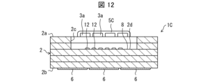
- Fig. 11 is a plan view of a wiring board 1C according to embodiment 4.
- Fig. 12 is a cross-sectional view taken along line XII-XII shown in Fig. 11.
- the wiring board 1C may include multiple mounting pads 3a.
- the mounting pads 3a are an example of the first connection portion in the [Summary] section described below.
- the wiring board 1C may include multiple intermediate patterns 4a extending from each mounting pad 3a along the first main surface 2a.
- the multiple intermediate patterns 4a extending from each of the multiple mounting pads 3a may be covered by a series of insulating films 5C.
- the intermediate patterns 4a are an example of intermediate conductors in the [Summary] section described below.
- Each of the multiple intermediate patterns 4a is connected to a multiple wiring conductor 7C.
- Each of the multiple wiring conductors 7C extends in a direction perpendicular to the first main surface 2a and has a first via conductor 7d connected to the multiple intermediate patterns 4a.
- the multiple mounting pads 3a are arranged separately on the first main surface 2a. Therefore, in the fourth embodiment, the first connection object may be an electronic component such as a capacitor or a large element such as an image sensor arranged in the center of the board. In other words, the mounting pad 3a connected to the first connection object can be used as a pad for surface mounting the component or a pad for wire bonding to the element.
- the multiple intermediate patterns 4a may be covered with one insulating film 5C as shown in FIG. 11. The aspect in which the multiple intermediate patterns 4a are covered with one insulating film 5C is easy to manufacture and can reduce the undulations caused by the insulating film 5C on the first main surface 2a. Alternatively, the multiple intermediate patterns 4a may each be individually covered with the insulating film 5C. When the multiple mounting pads 3a are located apart from each other, covering each of them individually can reduce the amount of material used for the insulating film 5C and reduce the weight.
- the directions in which the multiple intermediate patterns 4a extend from the multiple mounting pads 3a may be different from each other.
- the multiple intermediate patterns 4a may extend in opposite directions, such that adjacent intermediate patterns 4a extend in opposite directions.
- a wiring board in aspect 1 of the present disclosure is a wiring board capable of electrical connection to each of a first connection object and a second connection object, and includes a substrate having a first main surface and a second main surface opposite the first main surface, a first connection portion located on the first main surface and capable of electrical connection to the first connection object, an intermediate conductor located on the first main surface and extending from the first connection portion along the first main surface, an insulating film covering the intermediate conductor, a second connection portion located on the second main surface and capable of electrical connection to the second connection object, and a wiring conductor connecting the intermediate conductor and the second connection portion, the wiring conductor extending in a first direction perpendicular to the first main surface and having a first via conductor connected to the intermediate conductor.
- the wiring board in aspect 2 of the present disclosure is the wiring board in aspect 1 above, further comprising an element mounting portion on which an element can be mounted, the first connection portion surrounds the element mounting portion when viewed from the first direction, and the intermediate conductor extends in a direction away from the element mounting portion.
- the wiring board in aspect 3 of the present disclosure is the wiring board in aspect 2 above, in which the board has a recess that opens onto the first main surface, the element mounting portion is located on the bottom surface of the recess, and the first connection portion is located along the periphery of the recess.
- the wiring board in aspect 4 of the present disclosure is the wiring board in any one of aspects 1 to 3 above, further comprising a metal plating film covering the first connection portion.
- the wiring board in aspect 5 of the present disclosure is the wiring board in any one of aspects 1 to 4 above, in which the insulating film contains the same material as the substrate.
- the wiring board in aspect 6 of the present disclosure is the wiring board in aspect 5 above, in which the material is ceramic.
- the wiring board in aspect 7 of the present disclosure is the wiring board in any one of aspects 2 to 6 above, in which the insulating film is located only outside the area surrounded by the first connection portion.
- the wiring board in aspect 8 of the present disclosure is the wiring board in any one of aspects 2 to 7 above, in which the insulating film is located outside the first connection portion.
- a wiring board in aspect 9 of the present disclosure is a wiring board in any one of aspects 1 to 8 above, in which the first via conductor penetrates the board from the first main surface to the second main surface and is connected to the second connection portion.
- the wiring board in aspect 10 of the present disclosure is the wiring board in any one of aspects 1 to 9 above, wherein the wiring conductor further includes a second via conductor that extends in the first direction, is connected to the second connection portion, and is positioned so as not to overlap the first via conductor when viewed from the first direction, and an interlayer conductor that extends along a direction parallel to the first main surface.
- the wiring board in aspect 11 of the present disclosure is the wiring board in aspect 3 above, further comprising a third connection portion capable of electrically connecting to the first connection object, and a second wiring conductor connecting the third connection portion and the first connection portion, the recess having a middle step portion located between the bottom surface and the first main surface, and the third connection portion located above the middle step portion.
- the wiring board in aspect 12 of the present disclosure is the wiring board in any one of aspects 1 to 11 above, and includes a plurality of the first connection portions.
- the wiring board in aspect 13 of the present disclosure is the wiring board in aspect 12 above, in which the intermediate conductors extending from each of the first connection parts are covered with a series of insulating films.
Landscapes
- Engineering & Computer Science (AREA)
- Microelectronics & Electronic Packaging (AREA)
- Manufacturing & Machinery (AREA)
- Production Of Multi-Layered Print Wiring Board (AREA)
Priority Applications (1)
| Application Number | Priority Date | Filing Date | Title |
|---|---|---|---|
| JP2025501176A JPWO2024172068A1 (https=) | 2023-02-17 | 2024-02-14 |
Applications Claiming Priority (2)
| Application Number | Priority Date | Filing Date | Title |
|---|---|---|---|
| JP2023023686 | 2023-02-17 | ||
| JP2023-023686 | 2023-02-17 |
Publications (1)
| Publication Number | Publication Date |
|---|---|
| WO2024172068A1 true WO2024172068A1 (ja) | 2024-08-22 |
Family
ID=92419940
Family Applications (1)
| Application Number | Title | Priority Date | Filing Date |
|---|---|---|---|
| PCT/JP2024/004997 Ceased WO2024172068A1 (ja) | 2023-02-17 | 2024-02-14 | 配線基板 |
Country Status (2)
| Country | Link |
|---|---|
| JP (1) | JPWO2024172068A1 (https=) |
| WO (1) | WO2024172068A1 (https=) |
Citations (4)
| Publication number | Priority date | Publication date | Assignee | Title |
|---|---|---|---|---|
| JPH08250651A (ja) * | 1995-03-10 | 1996-09-27 | Nippon Steel Corp | 半導体パッケージ |
| JPH11145333A (ja) * | 1997-09-02 | 1999-05-28 | Oki Electric Ind Co Ltd | 半導体装置 |
| JP2002198452A (ja) * | 2000-12-27 | 2002-07-12 | Kyocera Corp | 電子部品収納用セラミックパッケージ及び電子部品装置 |
| JP2015096882A (ja) * | 2013-11-15 | 2015-05-21 | セイコーエプソン株式会社 | 電気光学装置および投射型表示装置 |
-
2024
- 2024-02-14 WO PCT/JP2024/004997 patent/WO2024172068A1/ja not_active Ceased
- 2024-02-14 JP JP2025501176A patent/JPWO2024172068A1/ja active Pending
Patent Citations (4)
| Publication number | Priority date | Publication date | Assignee | Title |
|---|---|---|---|---|
| JPH08250651A (ja) * | 1995-03-10 | 1996-09-27 | Nippon Steel Corp | 半導体パッケージ |
| JPH11145333A (ja) * | 1997-09-02 | 1999-05-28 | Oki Electric Ind Co Ltd | 半導体装置 |
| JP2002198452A (ja) * | 2000-12-27 | 2002-07-12 | Kyocera Corp | 電子部品収納用セラミックパッケージ及び電子部品装置 |
| JP2015096882A (ja) * | 2013-11-15 | 2015-05-21 | セイコーエプソン株式会社 | 電気光学装置および投射型表示装置 |
Also Published As
| Publication number | Publication date |
|---|---|
| JPWO2024172068A1 (https=) | 2024-08-22 |
Similar Documents
| Publication | Publication Date | Title |
|---|---|---|
| CN104412722B (zh) | 布线基板、电子装置以及发光装置 | |
| JP7210191B2 (ja) | 電子素子実装用基板、電子装置、および電子モジュール | |
| EP3680211B1 (en) | Sensor unit and method of interconnecting a substrate and a carrier | |
| WO2024172068A1 (ja) | 配線基板 | |
| JP7307161B2 (ja) | 電子素子実装用基板、電子装置、および電子モジュール | |
| US10681831B2 (en) | Electronic component mounting board, electronic device, and electronic module | |
| JP4803917B2 (ja) | 圧力検出装置用パッケージ | |
| JP7011563B2 (ja) | 回路基板および電子部品 | |
| CN110291628B (zh) | 布线基板、电子装置及电子模块 | |
| CN114175233B (zh) | 电子元件安装用基板、电子装置、电子模块以及电子元件安装用基板的制造方法 | |
| JP4794073B2 (ja) | 圧力検出装置用パッケージ | |
| JP7652908B2 (ja) | 電子素子実装用基板、電子装置および電子モジュール | |
| JP4582889B2 (ja) | 圧力検出装置用パッケージ | |
| JP4974424B2 (ja) | 圧力検出装置用パッケージ | |
| WO2026028559A1 (ja) | パッケージ素子 | |
| JP4794072B2 (ja) | 圧力検出装置用パッケージ | |
| JP2011124359A (ja) | 回路素子 | |
| JP4925522B2 (ja) | 圧力検出装置用パッケージ | |
| JP2015076584A (ja) | 電子部品収納用パッケージ | |
| JPH08227947A (ja) | 半導体素子収納用パッケージ | |
| JP2000357851A (ja) | ワイヤーボンディング用回路基板と実装基板 | |
| JP2020123661A (ja) | 電子素子実装用基板、電子装置、および電子モジュール | |
| JPH08335648A (ja) | 半導体装置 | |
| JP2003065874A (ja) | 圧力検出装置用パッケージ | |
| JPS63170993A (ja) | 回路基板 |
Legal Events
| Date | Code | Title | Description |
|---|---|---|---|
| 121 | Ep: the epo has been informed by wipo that ep was designated in this application |
Ref document number: 24756909 Country of ref document: EP Kind code of ref document: A1 |
|
| ENP | Entry into the national phase |
Ref document number: 2025501176 Country of ref document: JP Kind code of ref document: A |
|
| WWE | Wipo information: entry into national phase |
Ref document number: 2025501176 Country of ref document: JP |
|
| NENP | Non-entry into the national phase |
Ref country code: DE |
|
| 122 | Ep: pct application non-entry in european phase |
Ref document number: 24756909 Country of ref document: EP Kind code of ref document: A1 |