WO2024171697A1 - 半導体パッケージ基板 - Google Patents
半導体パッケージ基板 Download PDFInfo
- Publication number
- WO2024171697A1 WO2024171697A1 PCT/JP2024/001086 JP2024001086W WO2024171697A1 WO 2024171697 A1 WO2024171697 A1 WO 2024171697A1 JP 2024001086 W JP2024001086 W JP 2024001086W WO 2024171697 A1 WO2024171697 A1 WO 2024171697A1
- Authority
- WO
- WIPO (PCT)
- Prior art keywords
- core substrate
- semiconductor package
- less
- substrate
- package substrate
- Prior art date
- Legal status (The legal status is an assumption and is not a legal conclusion. Google has not performed a legal analysis and makes no representation as to the accuracy of the status listed.)
- Ceased
Links
Images

Classifications
-
- H—ELECTRICITY
- H05—ELECTRIC TECHNIQUES NOT OTHERWISE PROVIDED FOR
- H05K—PRINTED CIRCUITS; CASINGS OR CONSTRUCTIONAL DETAILS OF ELECTRIC APPARATUS; MANUFACTURE OF ASSEMBLAGES OF ELECTRICAL COMPONENTS
- H05K3/00—Apparatus or processes for manufacturing printed circuits
- H05K3/46—Manufacturing multilayer circuits
-
- H—ELECTRICITY
- H10—SEMICONDUCTOR DEVICES; ELECTRIC SOLID-STATE DEVICES NOT OTHERWISE PROVIDED FOR
- H10W—GENERIC PACKAGES, INTERCONNECTIONS, CONNECTORS OR OTHER CONSTRUCTIONAL DETAILS OF DEVICES COVERED BY CLASS H10
- H10W70/00—Package substrates; Interposers; Redistribution layers [RDL]
- H10W70/60—Insulating or insulated package substrates; Interposers; Redistribution layers
-
- H—ELECTRICITY
- H10—SEMICONDUCTOR DEVICES; ELECTRIC SOLID-STATE DEVICES NOT OTHERWISE PROVIDED FOR
- H10W—GENERIC PACKAGES, INTERCONNECTIONS, CONNECTORS OR OTHER CONSTRUCTIONAL DETAILS OF DEVICES COVERED BY CLASS H10
- H10W70/00—Package substrates; Interposers; Redistribution layers [RDL]
- H10W70/60—Insulating or insulated package substrates; Interposers; Redistribution layers
- H10W70/67—Insulating or insulated package substrates; Interposers; Redistribution layers characterised by their insulating layers or insulating parts
- H10W70/68—Shapes or dispositions thereof
Definitions
- the present invention relates to a semiconductor package substrate.
- the tallest component in a semiconductor package is the core substrate in the semiconductor package substrate, so by reducing the height of this core substrate, the height of the semiconductor package can be reduced efficiently.
- the core substrate of a conventional semiconductor package is made of, for example, a composite of resin and glass cloth (see, for example, Patent Document 1), and the height of the semiconductor package has been reduced by reducing the thickness of this core substrate.
- the present invention aims to provide a low-profile semiconductor package substrate that allows holes to be drilled without causing cracks in the core substrate.
- the present invention is as follows. [1] A semiconductor package substrate having a core substrate having a through hole connecting both main surfaces, and a conductive layer provided on both main surfaces of the core substrate and at least a portion of the through hole, wherein the core substrate contains 25% by mass or more of a ceramic having cleavage in one direction, and the thickness of the core substrate is 100 to 1500 ⁇ m.
- [2] The semiconductor package substrate according to [1] above, wherein the content of the ceramic in the core substrate is 40 mass % or more.
- [3] The semiconductor package substrate according to [1] or [2] above, wherein the number average hole diameter of the through holes is 50 to 300 ⁇ m, and the number of the through holes in the core substrate is 10 or more per 0.001 m2 .
- [4] The semiconductor package substrate according to any one of [1] to [3] above, wherein the core substrate has a relative dielectric constant Dk of 6.0 or less at 10 GHz and a dielectric loss tangent tan ⁇ of 0.0100 or less at 10 GHz.
- the present invention provides a low-profile semiconductor package substrate that allows holes to be drilled without causing cracks in the core substrate.
- FIG. 1 is a schematic cross-sectional view showing an example of a semiconductor package including a semiconductor package substrate of the present invention.
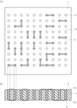
- FIG. 2(a) is a schematic plan view showing an example of a core substrate in a semiconductor package substrate of the present invention
- FIG. 2(b) is a schematic cross-sectional view showing an example of a core substrate in a semiconductor package substrate of the present invention.
- the description "preferably 10 to 90, more preferably 30 to 60” can be combined with the “preferable lower limit (10)” and the “more preferable upper limit (60)” to obtain “10 to 60.”
- the upper limit or lower limit of the numerical range may be replaced with a value shown in the examples.
- machinable ceramics refers to “ceramics with excellent machinability” and have a lower expansion coefficient and higher rigidity than ordinary ceramics.
- the semiconductor package substrate of the present invention is a part of a semiconductor package, and comprises a core substrate having a through hole connecting both main surfaces, and a conductive layer provided on both main surfaces of the core substrate and on at least a portion of the through hole, and may further comprise other components such as a resin layer as necessary.
- FIG. 1 is a schematic cross-sectional view showing an example of a semiconductor package including a semiconductor package substrate of the present invention.
- a semiconductor package (IC-PKG) 100 connects a motherboard (not shown), which is a type of printed circuit board (PCB), to a semiconductor chip 6, and has a semiconductor package substrate 10, solder 4, underfill 11, and solder balls 40.
- the solder 4 is provided between the semiconductor chip 6 and the semiconductor package substrate 10 to electrically connect the semiconductor chip 6 and the semiconductor package substrate 10 .
- the solder 40 is provided between the semiconductor package substrate 10 and a motherboard (not shown) to electrically connect the semiconductor package substrate 10 and the motherboard (not shown).
- the motherboard (not shown) is an insulating substrate on which conductor wiring is performed and electronic components are soldered.
- the semiconductor chip 6 examples include semiconductor chips made of silicon, such as “discrete semiconductors,””ICs (integrated circuits),” and “LSIs (large scale integrated circuits).”
- the underfill 11 may be provided between the semiconductor chip 6 and the semiconductor package substrate 10, and may include the solder 4.
- the underfill 11 includes, for example, an epoxy resin.
- the semiconductor package substrate 10 includes a core substrate 1, a conductive layer 3 provided on both main surfaces 1a and 1b of the core substrate 1 and a part of the through hole 2, a first interlayer insulating material (build-up film) 7 provided on one main surface 1a of the core substrate 1, a second interlayer insulating material (build-up film) 8 provided on the other main surface 1b of the core substrate 1, and a solder resist 9 provided on the outside of the first interlayer insulating material 7 and the second interlayer insulating material 8.
- a first interlayer insulating material (build-up film) 7 provided on one main surface 1a of the core substrate 1
- a second interlayer insulating material (build-up film) 8 provided on the other main surface 1b of the core substrate 1
- solder resist 9 provided on the outside of the first interlayer insulating material 7 and the second interlayer insulating material 8.
- the first interlayer insulating material 7 is provided with a conductive layer 3 connected to the solder 4
- the second interlayer insulating material 8 is provided with a conductive layer 3 connected to the solder ball 40.
- the through hole 2 may be filled with a hole-filling resin as shown in Fig. 1.
- FIG. 2(a) is a schematic plan view showing an example of a core substrate in a semiconductor package substrate of the present invention
- FIG. 2(b) is a schematic cross-sectional view showing an example of a core substrate in a semiconductor package substrate of the present invention.
- the core substrate 1 is provided with a through hole 2 connecting both main surfaces 1a, 1b of the core substrate 1.
- Both main surfaces 1a, 1b of the core substrate 1 and a part of the through hole 2 are provided with a conductive layer 3, which will be described later.
- the conductive layers 3 provided on both main surfaces 1a, 1b of the core substrate 1 are formed by patterning copper foil formed on both sides of a prepreg in a copper clad laminate (CCL) by etching or the like.
- the core substrate contains a ceramic having cleavage in one direction (hereinafter, may be simply referred to as "ceramic"), and further contains other components such as glass, if necessary.
- the core substrate can be used not only as a copper-clad laminate for semiconductor packages, but also as other copper-clad laminates.
- Having cleavage in one direction means “having the property of the crystal cracking or peeling along one specific direction to present a smooth surface,” and in one embodiment means "a cut surface obtained by cutting a superlattice in which two crystal unit cells are arranged in each of the length, width, and height directions, which contains elements other than silicon (Si), aluminum (Al), and oxygen (O), and which has only one cut surface that is electrically neutral.”
- Ceramics having cleavage in one direction include machinable ceramics such as boron nitride (BN); diamond, graphite; layered silicates such as mica, talc, and montmorillonite; dichalcogenides such as titanium disulfide; boehmite; divalent metal hydroxides such as magnesium hydroxide; layered double hydroxides such as hydrotalcite; layered titanates; layered phosphates such as hydroxyapatite. These may be used alone or in combination of two or more.
- machinable ceramics such as boron nitride (BN); diamond, graphite; layered silicates such as mica, talc, and montmorillonite; dichalcogenides such as titanium disulfide; boehmite; divalent metal hydroxides such as magnesium hydroxide; layered double hydroxides such as hydrotalcite; layered titanates; layered phosphates such as hydroxyapatite. These may be used alone or in combination of two
- mica and boron nitride are preferred, and more preferably contain boron nitride (BN) crystals, and even more preferably contain a mixture of mica crystals and boron nitride (BN) crystals, in view of having a surface with extremely low bond strength and improving machinability.
- X-ray crystal structure analysis prowder X-ray diffraction (PXRD) measurement
- PXRD X-ray X-ray diffraction
- PXRD X-ray diffraction
- Powder X-ray diffraction (PXRD) measurement conditions Powder X-ray diffraction (PXRD) is measured under the following conditions, and the resultant measurement is used to carry out Rietveld analysis to identify the precipitated crystals.
- the precipitated crystals are identified using diffraction peak patterns recorded in the ICSD Inorganic Crystal Structure Database and the ICDD Powder Diffraction Database.
- the number average particle size of the ceramic particles used to prepare the core substrate is not particularly limited, but from the viewpoint of improving processability, it is preferably 0.05 ⁇ m or more, more preferably 0.10 ⁇ m or more, and particularly preferably 0.50 ⁇ m or more, and from the viewpoint of increasing the density of the core substrate, it is preferably 10.00 ⁇ m or less, more preferably 5.00 ⁇ m or less, and particularly preferably 1.00 ⁇ m or less.
- the number average particle size of the ceramic particles used to prepare the core substrate is not particularly limited, but is preferably 0.05 to 10.00 ⁇ m, more preferably 0.10 to 5.00 ⁇ m, and particularly preferably 0.50 to 1.00 ⁇ m.
- the number average particle size can be determined by a laser diffraction particle size distribution analyzer.
- the components other than the ceramics in the core substrate are not particularly limited, and examples include glasses such as soda lime glass, alkali aluminosilicate glass, and borosilicate glass; resins such as fluororesins, epoxy resins, and polyimides; oxides such as silicon oxide; and minerals such as spodumene; and may be used alone or in combination of two or more.
- glasses such as soda lime glass, alkali aluminosilicate glass, and borosilicate glass
- resins such as fluororesins, epoxy resins, and polyimides
- oxides such as silicon oxide
- minerals such as spodumene
- the number average particle size of the glass particles used to prepare the core substrate is not particularly limited, but from the viewpoint of homogeneously mixing the powder, it is preferably 0.05 ⁇ m or more, more preferably 0.10 ⁇ m or more, and particularly preferably 0.50 ⁇ m or more, and from the viewpoint of increasing the density of the core substrate, it is preferably 10.00 ⁇ m or less, more preferably 5.00 ⁇ m or less, and particularly preferably 1.00 ⁇ m or less.
- the number average particle size of the glass particles used to prepare the core substrate is not particularly limited, but is preferably 0.05 to 10.00 ⁇ m, more preferably 0.10 to 5.00 ⁇ m, and particularly preferably 0.50 to 1.00 ⁇ m.
- the number average particle size can be determined by a laser diffraction particle size distribution analyzer.
- the content of ceramics in the core substrate is not particularly limited as long as it is 25% by mass or more, but from the viewpoint of achieving high processability, it is preferably 30% by mass or more, more preferably 35% by mass or more, even more preferably 40% by mass or more, particularly preferably 50% by mass or more, and most preferably 60% by mass or more, and from the viewpoint of increasing Young's modulus, controlling the expansion coefficient, and reducing warpage of the substrate, it is preferably 99% by mass or less, more preferably 95% by mass or less, even more preferably 90% by mass or less, and particularly preferably 80% by mass or less.
- the content of ceramics in the core substrate may be 100% by mass.
- the content of the ceramic in the core substrate is not particularly limited as long as it is 25% by mass or more, but is preferably 30 to 99% by mass, more preferably 35 to 95% by mass, even more preferably 40 to 90% by mass, particularly preferably 50 to 80% by mass, and most preferably 60 to 80% by mass.
- the sum of the ceramic content in the core substrate and the glass content in the core substrate is not particularly limited, but from the viewpoint of a high Young's modulus and low expansion coefficient of the core material, it is preferably 60 mass% or more, more preferably 70 mass% or more, even more preferably 75 mass% or more, even more preferably 80 mass% or more, even more preferably 90 mass% or more, and particularly preferably 100 mass%.
- the thickness of the core substrate is not particularly limited as long as it is 100 to 1500 ⁇ m, but from the viewpoint of preventing cracking of the substrate, it is preferably 120 ⁇ m or more, more preferably 160 ⁇ m or more, and particularly preferably 200 ⁇ m or more, and from the viewpoint of reducing the height of the IC-PKG, it is preferably 1400 ⁇ m or less, more preferably 1200 ⁇ m or less, even more preferably 1000 ⁇ m or less, even more preferably 800 ⁇ m or less, particularly preferably 700 ⁇ m or less, and most preferably 600 ⁇ m or less.
- the thickness of the core substrate is not particularly limited as long as it is 100 to 1500 ⁇ m, but is preferably 120 to 1400 ⁇ m, more preferably 160 to 1200 ⁇ m, even more preferably 160 to 1000 ⁇ m, still more preferably 160 to 800 ⁇ m, particularly preferably 200 to 700 ⁇ m, and most preferably 200 to 600 ⁇ m.
- the relative dielectric constant Dk of the core substrate at 10 GHz is not particularly limited, but from the viewpoint of narrowing the wiring space, it is preferably 7.0 or less, more preferably 6.0 or less, even more preferably 5.5 or less, even more preferably 5.3 or less, even more preferably 5.0 or less, even more preferably 4.8 or less, even more preferably 4.6 or less, even more preferably 4.5 or less, even more preferably 4.4 or less, even more preferably 4.3 or less, particularly preferably 4.2 or less, and most preferably 4.1 or less.
- the relative dielectric constant Dk is 2.0 or more.
- the relative dielectric constant Dk of the core substrate at 10 GHz is not particularly limited, but is preferably 2.0 to 7.0, more preferably 2.0 to 6.0, even more preferably 2.0 to 5.5, even more preferably 2.0 to 5.3, even more preferably 2.0 to 5.0, even more preferably 2.0 to 4.8, even more preferably 2.0 to 4.6, even more preferably 2.0 to 4.5, even more preferably 2.0 to 4.4, even more preferably 2.0 to 4.3, particularly preferably 2.0 to 4.2, and most preferably 2.0 to 4.1.
- the dielectric loss tangent tan ⁇ of the core substrate at 10 GHz is not particularly limited, but from the viewpoint of reducing electrical loss in the device, it is preferably 0.0100 or less, more preferably 0.0080 or less, even more preferably 0.0060 or less, particularly preferably 0.0050 or less, and most preferably 0.0040 or less. Generally, the dielectric loss tangent tan ⁇ is 0.0001 or more.
- the dielectric loss tangent tan ⁇ of the core substrate at 10 GHz is not particularly limited, but is preferably 0.0001 to 0.0100, more preferably 0.0001 to 0.0080, even more preferably 0.0001 to 0.0060, particularly preferably 0.0001 to 0.0050, and most preferably 0.0001 to 0.0040.
- the relative dielectric constant Dk and the dielectric loss tangent tan ⁇ at 10 GHz of the core substrate are measured by the method described in the Examples.
- the thermal expansion coefficient of the core substrate at ⁇ 50° C. to 200° C. is not particularly limited, but from the viewpoint of bringing the expansion coefficient closer to that of the semiconductor substrate and reducing warpage of the entire substrate, the coefficient is preferably 0.0 ppm/K or more, more preferably 0.4 ppm/K or more, even more preferably 0.8 ppm/K or more, even more preferably 1.5 ppm/K or more, even more preferably 2.0 ppm/K or more, even more preferably 2.5 ppm/K or more, even more preferably 3.0 ppm/K or more, particularly preferably 3.5 ppm/K or more, and most preferably 4.0 ppm/K or more.
- the coefficient is preferably 15.0 ppm/K or less, more preferably 13.0 ppm/K or less, even more preferably 11.0 ppm/K or less, even more preferably 10.0 ppm/K or less, still more preferably 9.0 ppm/K or less, particularly preferably 8.0 ppm/K or less, and most preferably 7.0 ppm/K or less.
- the thermal expansion coefficient of the core substrate at -50°C to 200°C is not particularly limited, but is preferably 0.0 to 15.0 ppm/K, more preferably 0.4 to 13.0 ppm/K, even more preferably 0.8 to 11.0 ppm/K, even more preferably 1.5 to 10.0 ppm/K, even more preferably 2.0 to 9.0 ppm/K or more, even more preferably 2.5 to 9.0 ppm/K, even more preferably 3.0 to 9.0 ppm/K, particularly preferably 3.5 to 8.0 ppm/K, and most preferably 4.0 to 7.0 ppm/K.
- the thermal expansion coefficient of the core substrate is measured by the method described in the examples.
- the Young's modulus of the core substrate is not particularly limited, but from the viewpoint of maintaining high rigidity and suppressing warping due to heat, it is preferably 10.0 GPa or more, more preferably 14.0 GPa or more, even more preferably 18.0 GPa or more, even more preferably 20.0 GPa or more, even more preferably 25.0 GPa or more, even more preferably 30.0 GPa or more, particularly preferably 35.0 GPa or more, and most preferably 40.0 GPa or more, and from the viewpoint of reducing the stress applied when the substrate warps, it is preferably 120.0 GPa or less, more preferably 100.0 GPa or less, even more preferably 80.0 GPa or less, particularly preferably 70.0 GPa or less, and most preferably 60.0 GPa or less.
- the Young's modulus of the core substrate is not particularly limited, but is preferably 10.0 to 120.0 GPa, more preferably 14.0 to 100.0 GPa, even more preferably 18.0 to 80.0 GPa, even more preferably 20.0 to 80.0 GPa, even more preferably 25.0 to 80.0 GPa, even more preferably 30.0 to 80.0 GPa, particularly preferably 35.0 to 70.0 GPa, and most preferably 40.0 to 60.0 GPa.
- the Young's modulus of the core substrate is measured by the method described in the Examples.
- the surface roughness Ra of the outermost surfaces of both main surfaces of the core substrate is not particularly limited, but from the viewpoint of obtaining sufficient processability, it is preferably 0.1 ⁇ m or more, more preferably 0.2 ⁇ m or more, and particularly preferably 0.3 ⁇ m or more, and from the viewpoint of flattening the wiring layer and reducing the skin effect, it is preferably 100 ⁇ m or less, more preferably 50 ⁇ m or less, even more preferably 10.0 ⁇ m or less, particularly preferably 5.0 ⁇ m or less, and most preferably 1.0 ⁇ m or less.
- the surface roughness Ra of the outermost surfaces of both main surfaces of the core substrate is not particularly limited, but is preferably 0.1 to 100 ⁇ m, more preferably 0.2 to 50 ⁇ m, even more preferably 0.2 to 10.0 ⁇ m, particularly preferably 0.3 to 5.0 ⁇ m, and most preferably 0.3 to 1.0 ⁇ m.
- the surface roughness Ra of the outermost surfaces of both main surfaces of the core substrate is measured by the method described in the examples.
- the core substrate is provided with a through hole connecting both main surfaces.
- the number average pore size of the through holes in the core substrate is not particularly limited, but from the viewpoint of obtaining a hole shape close to a perfect circle, it is preferably 50 ⁇ m or more, more preferably 75 ⁇ m or more, and particularly preferably 100 ⁇ m or more, and from the viewpoint of producing fine wiring and producing a densified substrate, it is preferably 500 ⁇ m or less, more preferably 400 ⁇ m or less, and particularly preferably 300 ⁇ m or less.
- the number average pore size of the through holes in the core substrate is not particularly limited, but is preferably 50 to 500 ⁇ m, more preferably 75 to 400 ⁇ m, and particularly preferably 100 to 300 ⁇ m.
- the number of through holes in the core substrate per unit area is not particularly limited, but from the viewpoint of producing a highly densified substrate, it is preferably 10 or more, more preferably 30 or more, even more preferably 50 or more, even more preferably 70 or more, even more preferably 90 or more, and particularly preferably 100 or more.
- the through holes are formed by a mechanical drilling method, it is preferable that the through holes can be formed continuously without damaging the drill or causing cracks in the core substrate.
- the conductive layer is provided on both main surfaces of the core substrate and on at least a part of the through hole.
- the conductive material in the conductive layer is not particularly limited, and examples thereof include copper, titanium, silver, nickel, chromium, tin, indium, gallium, and alloy materials thereof.
- the thickness of the conductive layer is not particularly limited, but from the viewpoint of ensuring sufficient conductivity, it is preferably 5 nm or more, more preferably 10 nm or more, and particularly preferably 50 nm or more, and from the viewpoint of reducing the height of the entire package, it is preferably 1000 nm or less, more preferably 500 nm or less, and particularly preferably 300 nm or less.
- the thickness of the conductive layer is not particularly limited, but is preferably 5 to 1000 nm, more preferably 10 to 500 nm, and particularly preferably 50 to 300 nm.
- the first interlayer insulating material 7 is provided, for example, between a core substrate 1 and a solder 4. Also, as shown in Fig. 1, a conductive layer 3 may be provided inside the first interlayer insulating material 7.
- the first interlayer insulating material 7 contains, for example, a resin and an inorganic filler.
- the second interlayer insulating material 8 is provided, for example, between the core substrate 1 and the solder balls 40. Also, as shown in Fig. 1, a conductive layer 3 may be provided inside the second interlayer insulating material 8.
- the second resin layer 8 contains, for example, a resin and an inorganic filler.
- Examples 1 to 7, 11 to 17, 25 to 28, 31 to 34, and 36 to 39 are working examples, and Examples 8 to 10, 18 to 24, 29 to 30, and 35 are comparative examples.
- crystals selected from the group consisting of mica, wollastonite, boron nitride (BN), alumina, and spodumene were mixed with silica glass as glass in the ratios shown in Tables 1 to 4.
- fluorine mica KMg 3 AlSi 3 O 10 F 2
- NK-M number average particle size 12 ⁇ m
- CaSiO 3 manufactured by Keiwa Fine Material Co., Ltd., product name: K-330, number average particle size 19 ⁇ m
- BN (manufacturer: Showa Denko Ceramics Co., Ltd., product name: UHP-S2, number average particle size 0.5 ⁇ m) was used as boron nitride
- Al 2 O 3 manufactured by Taiheiyo Random Co., Ltd., product name:
- the mixed powder was molded and sintered at a temperature between 800°C and 1200°C to obtain sheets 1 to 39 with thicknesses of 0.1 to 3.0 mm. Polishing was performed in the process from sintering to obtaining the thin plate.
- sheet 35 a resin-impregnated glass cloth was used.
- the obtained sheets 1 to 39 were processed into plate-shaped samples with a length of 60.0 mm, a width of 10.0 mm, and a thickness of 0.7 mm, and the 60.0 mm ⁇ 10.0 mm surface was polished to a mirror finish. Measurements were performed by the cavity resonator method according to JIS R1602:1995.
- the obtained sheets 1 to 39 were processed into plate-shaped samples having a length of 15.0 mm, a width of 5.0 mm, and a thickness of 0.7 mm, and the 15.0 mm x 5.0 mm surface was polished to a mirror finish.
- the thermal expansion coefficient was measured at -50°C to 200°C using a differential expansion thermomechanical analyzer in accordance with JIS R1618:2002.
- the surface roughness Ra of 200 ⁇ m square was calculated as observed when the entire area was observed with a 100x lens using a laser micro microscope VK-X200 manufactured by Keyence Corporation.
- the drilling of the obtained sheets 1 to 39 was performed while changing the drill diameter from 100 to 300 ⁇ m according to the number average hole diameter of the holes.
- the pitch between the holes was three times the number average hole diameter of the holes, and the drill rotation speed was 100 krpm and the drill feed speed was 0.3 m/min by the mechanical drilling method.
- the drill was made of SUS material.
- the operation of continuously drilling holes was performed until the drill broke, and when 100 holes could be continuously drilled without generating cracks, the test was stopped as it was deemed that the drill had sufficient hole drilling ability.
- the obtained sheets 1 to 39 were processed into samples of 300 mm square x 0.3 mm.
- copper electrodes were formed on a 300 mm square x 0.3 mm core substrate (sample), a silicon substrate was attached to the copper electrodes using tin solder balls, and the temperature was changed by 200°C from -40°C to 160°C for three cycles. If the solder balls did not come off the silicon substrate or core substrate (sample), it was marked as "A,” and if the solder balls came off the silicon substrate or core substrate (sample) under the same conditions, it was marked as "B.”
- Examples 1 to 10 sheets were produced as core substrates by varying the ratio of mica crystals having cleavage in one direction to glass.
- Examples 8 to 10 were comparative examples, in which the content of mica crystals in the core substrate was 20% by mass or less, and through holes could not be successfully drilled, and therefore they could not be used as materials for semiconductor packages.
- Example 11 to 19 In Examples 11 to 19, the ratio of boron nitride (BN) crystals having cleavage in one direction to glass was changed to produce a sheet as a core substrate.
- Examples 18 to 19 were comparative examples, in which the content of BN crystals in the core substrate was 20% by mass or less, and holes could not be drilled well, so they could not be used as materials for semiconductor packages.
- Examples 20 to 24 sheets as core substrates were prepared by changing the type of ceramics contained. In Examples 20 and 24, sheets were prepared containing 80 mass% of wollastonite and alumina, which are generally said to be crystals with excellent grindability. In the sheets prepared in Examples 20 and 24, neither wollastonite nor alumina is a ceramic having cleavage in one direction, so through holes could not be drilled well and they could not be used as materials for semiconductor packages. In addition, in Examples 21 to 23, sheets as core substrates were prepared by changing the content ratio of crystals. Even if the crystal ratio was changed, through holes could not be drilled well and they could not be used as materials for semiconductor packages. In other words, it can be seen that no matter what the crystal ratio is, if the crystal species is not appropriate, through holes cannot be formed.
- Example 25 to 30 sheets were produced as core substrates with different thicknesses.
- Examples 25 to 28 are working examples, and it was confirmed that 100 through holes per 0.0001 m2 were drilled in both 0.2 mm and 1.0 mm thick sheets, and that the sheets could be used as materials for semiconductor packages.
- Examples 29 and 30 are comparative examples, and the 3.0 mm thick sheet was too thick, so the drill broke before drilling 100 through holes, and the through holes could not be drilled successfully.
- Examples 31 to 34 are working examples, and it was confirmed that 100 through holes per 0.0001 m2 could be drilled using a drill, regardless of whether the number average pore diameter was 100 ⁇ m or 300 ⁇ m, and that the material could be used as a material for semiconductor packages.
- Example 35 is a comparative example, in which a sheet was prepared as a core substrate made of conventional glass cloth and resin. Although 100 through holes per 0.0001 m2 could be drilled using a drill, the sample was significantly warped in a thermal warping test, and could not be used as a material for semiconductor packages.
- Examples 36 to 38 are working examples, and it was confirmed that even when various other components (silicon oxide (SiO 2 ), spodumene) were added, 100 through holes per 0.0001 m 2 could be drilled, and the material could be used as a material for semiconductor packages.
- SiO 2 silicon oxide
- spodumene spodumene
- Example 39 is an embodiment, and it was confirmed that even when a mixture of mica crystals and boron nitride (BN) crystals was used as the ceramic, 100 through holes were drilled per 0.0001 m2 , and the material could be used as a material for semiconductor packages.
- BN boron nitride
- a semiconductor package substrate having a core substrate with through holes connecting both main surfaces and a conductive layer provided on both main surfaces of the core substrate and at least a part of the through holes, in which the core substrate contains 25% by mass or more of ceramics having cleavage in one direction and the thickness of the core substrate is 100 to 1500 ⁇ m can provide a low-profile semiconductor package substrate in which holes can be machined without causing cracks in the core substrate.
- Example 2 it is considered that Examples 2, 11 to 17, and 39 are preferred, Examples 11 to 17 and 39 are more preferred, and Example 39 is a particularly preferred embodiment.
- the core substrate in the semiconductor package substrate of the present invention can be used not only for semiconductor packages as shown in FIG. 1, but also for antennas, filter devices, etc.
Landscapes
- Engineering & Computer Science (AREA)
- Manufacturing & Machinery (AREA)
- Microelectronics & Electronic Packaging (AREA)
- Production Of Multi-Layered Print Wiring Board (AREA)
Priority Applications (1)
| Application Number | Priority Date | Filing Date | Title |
|---|---|---|---|
| JP2025500729A JPWO2024171697A1 (https=) | 2023-02-17 | 2024-01-17 |
Applications Claiming Priority (2)
| Application Number | Priority Date | Filing Date | Title |
|---|---|---|---|
| JP2023-023321 | 2023-02-17 | ||
| JP2023023321 | 2023-02-17 |
Publications (1)
| Publication Number | Publication Date |
|---|---|
| WO2024171697A1 true WO2024171697A1 (ja) | 2024-08-22 |
Family
ID=92421518
Family Applications (1)
| Application Number | Title | Priority Date | Filing Date |
|---|---|---|---|
| PCT/JP2024/001086 Ceased WO2024171697A1 (ja) | 2023-02-17 | 2024-01-17 | 半導体パッケージ基板 |
Country Status (2)
| Country | Link |
|---|---|
| JP (1) | JPWO2024171697A1 (https=) |
| WO (1) | WO2024171697A1 (https=) |
Citations (8)
| Publication number | Priority date | Publication date | Assignee | Title |
|---|---|---|---|---|
| JPH11186677A (ja) * | 1997-12-25 | 1999-07-09 | Shin Etsu Polymer Co Ltd | プリント配線板用積層板 |
| JP2001185848A (ja) * | 1999-12-22 | 2001-07-06 | Sony Corp | 多層回路基板およびその製造方法 |
| JP2002151848A (ja) * | 2000-11-10 | 2002-05-24 | Mitsubishi Plastics Ind Ltd | ビルドアップ多層プリント配線基板用コア基板 |
| JP2002353580A (ja) * | 2001-05-23 | 2002-12-06 | Matsushita Electric Ind Co Ltd | 回路基板用絶縁材,回路基板およびその製造方法 |
| JP2003124397A (ja) * | 2001-10-10 | 2003-04-25 | Tokuyama Corp | 基板及びその製造方法 |
| JP2012049423A (ja) * | 2010-08-30 | 2012-03-08 | Sumitomo Bakelite Co Ltd | 回路基板、半導体装置、回路基板の製造方法および半導体装置の製造方法 |
| JP2018120918A (ja) * | 2017-01-24 | 2018-08-02 | 日本特殊陶業株式会社 | セラミックパッケージ、電子部品装置、及びセラミックパッケージの製造方法 |
| JP7137292B2 (ja) * | 2019-03-15 | 2022-09-14 | 京セラ株式会社 | 配線基板およびその製造方法 |
-
2024
- 2024-01-17 JP JP2025500729A patent/JPWO2024171697A1/ja active Pending
- 2024-01-17 WO PCT/JP2024/001086 patent/WO2024171697A1/ja not_active Ceased
Patent Citations (8)
| Publication number | Priority date | Publication date | Assignee | Title |
|---|---|---|---|---|
| JPH11186677A (ja) * | 1997-12-25 | 1999-07-09 | Shin Etsu Polymer Co Ltd | プリント配線板用積層板 |
| JP2001185848A (ja) * | 1999-12-22 | 2001-07-06 | Sony Corp | 多層回路基板およびその製造方法 |
| JP2002151848A (ja) * | 2000-11-10 | 2002-05-24 | Mitsubishi Plastics Ind Ltd | ビルドアップ多層プリント配線基板用コア基板 |
| JP2002353580A (ja) * | 2001-05-23 | 2002-12-06 | Matsushita Electric Ind Co Ltd | 回路基板用絶縁材,回路基板およびその製造方法 |
| JP2003124397A (ja) * | 2001-10-10 | 2003-04-25 | Tokuyama Corp | 基板及びその製造方法 |
| JP2012049423A (ja) * | 2010-08-30 | 2012-03-08 | Sumitomo Bakelite Co Ltd | 回路基板、半導体装置、回路基板の製造方法および半導体装置の製造方法 |
| JP2018120918A (ja) * | 2017-01-24 | 2018-08-02 | 日本特殊陶業株式会社 | セラミックパッケージ、電子部品装置、及びセラミックパッケージの製造方法 |
| JP7137292B2 (ja) * | 2019-03-15 | 2022-09-14 | 京セラ株式会社 | 配線基板およびその製造方法 |
Also Published As
| Publication number | Publication date |
|---|---|
| JPWO2024171697A1 (https=) | 2024-08-22 |
Similar Documents
| Publication | Publication Date | Title |
|---|---|---|
| US20020094929A1 (en) | Glass ceramic sintered product and process for production thereof | |
| US7838107B2 (en) | Aluminum-silicon carbide composite | |
| US7605101B2 (en) | Laminate, ceramic substrate and method for making the ceramic substrate | |
| US20080242787A1 (en) | Eucryptite ceramic filler and insulating composite material containing the same | |
| JPH04243962A (ja) | 多層セラミックパッケージ用低誘電性無機組成物、及びその調製方法 | |
| WO2014191421A1 (en) | Multilayer wiring substrate | |
| US5141899A (en) | Low dielectric inorganic composition for multilayer ceramic package containing titanium silicate glass and crystal inhibitor | |
| US5316985A (en) | Suppression of crystal growth in low dielectric inorganic composition using ultrafine alumina | |
| EP1364921B1 (en) | Glass ceramic composition, glass ceramic sintered material and ceramic multilayer substrate | |
| Sebastian et al. | High temperature cofired ceramic (HTCC), low temperature cofired ceramic (LTCC), and ultralow temperature cofired ceramic (ULTCC) materials | |
| JP2019161219A (ja) | ガラスセラミック誘電体 | |
| JP2020182006A (ja) | ガラス回路基板 | |
| JP2002111210A (ja) | 配線基板およびその製造方法 | |
| WO2024171697A1 (ja) | 半導体パッケージ基板 | |
| US12404209B2 (en) | Laminate | |
| JP4452846B2 (ja) | 金属−セラミックス接合基板及びその製造方法 | |
| JP4422453B2 (ja) | 配線基板 | |
| JPH09241068A (ja) | 低温焼成セラミックス基板 | |
| WO2022168624A1 (ja) | 積層ガラスセラミック誘電体材料、焼結体、焼結体の製造方法及び高周波用回路部材 | |
| TWI906014B (zh) | 配線基板及半導體裝置 | |
| TWI920880B (zh) | 複合配線基板及半導體裝置 | |
| TWI906015B (zh) | 配線基板及半導體裝置 | |
| WO2026070798A1 (ja) | 積層基板、配線基板、積層基板の製造方法、配線基板の製造方法、及び半導体パッケージ | |
| WO2025142900A1 (ja) | 複合配線基板および半導体デバイス | |
| WO2026070217A1 (ja) | 積層基板、配線基板、積層基板の製造方法、配線基板の製造方法、及び半導体パッケージ |
Legal Events
| Date | Code | Title | Description |
|---|---|---|---|
| 121 | Ep: the epo has been informed by wipo that ep was designated in this application |
Ref document number: 24756548 Country of ref document: EP Kind code of ref document: A1 |
|
| ENP | Entry into the national phase |
Ref document number: 2025500729 Country of ref document: JP Kind code of ref document: A |
|
| WWE | Wipo information: entry into national phase |
Ref document number: 2025500729 Country of ref document: JP |
|
| NENP | Non-entry into the national phase |
Ref country code: DE |
|
| 122 | Ep: pct application non-entry in european phase |
Ref document number: 24756548 Country of ref document: EP Kind code of ref document: A1 |