WO2024161644A1 - レーザ加工装置、半導体チップおよび半導体チップの製造方法 - Google Patents
レーザ加工装置、半導体チップおよび半導体チップの製造方法 Download PDFInfo
- Publication number
- WO2024161644A1 WO2024161644A1 PCT/JP2023/003638 JP2023003638W WO2024161644A1 WO 2024161644 A1 WO2024161644 A1 WO 2024161644A1 JP 2023003638 W JP2023003638 W JP 2023003638W WO 2024161644 A1 WO2024161644 A1 WO 2024161644A1
- Authority
- WO
- WIPO (PCT)
- Prior art keywords
- unit
- wafer
- outer door
- inner door
- door
- Prior art date
- Legal status (The legal status is an assumption and is not a legal conclusion. Google has not performed a legal analysis and makes no representation as to the accuracy of the status listed.)
- Ceased
Links
Images


Classifications
-
- H—ELECTRICITY
- H10—SEMICONDUCTOR DEVICES; ELECTRIC SOLID-STATE DEVICES NOT OTHERWISE PROVIDED FOR
- H10P—GENERIC PROCESSES OR APPARATUS FOR THE MANUFACTURE OR TREATMENT OF DEVICES COVERED BY CLASS H10
- H10P72/00—Handling or holding of wafers, substrates or devices during manufacture or treatment thereof
- H10P72/04—Apparatus for manufacture or treatment
- H10P72/0451—Apparatus for manufacturing or treating in a plurality of work-stations
- H10P72/0462—Apparatus for manufacturing or treating in a plurality of work-stations characterised by the construction of the processing chambers, e.g. modular processing chambers
-
- B—PERFORMING OPERATIONS; TRANSPORTING
- B23—MACHINE TOOLS; METAL-WORKING NOT OTHERWISE PROVIDED FOR
- B23K—SOLDERING OR UNSOLDERING; WELDING; CLADDING OR PLATING BY SOLDERING OR WELDING; CUTTING BY APPLYING HEAT LOCALLY, e.g. FLAME CUTTING; WORKING BY LASER BEAM
- B23K26/00—Working by laser beam, e.g. welding, cutting or boring
- B23K26/08—Devices involving relative movement between laser beam and workpiece
- B23K26/083—Devices involving movement of the workpiece in at least one axial direction
-
- B—PERFORMING OPERATIONS; TRANSPORTING
- B23—MACHINE TOOLS; METAL-WORKING NOT OTHERWISE PROVIDED FOR
- B23K—SOLDERING OR UNSOLDERING; WELDING; CLADDING OR PLATING BY SOLDERING OR WELDING; CUTTING BY APPLYING HEAT LOCALLY, e.g. FLAME CUTTING; WORKING BY LASER BEAM
- B23K26/00—Working by laser beam, e.g. welding, cutting or boring
- B23K26/36—Removing material
- B23K26/362—Laser etching
- B23K26/364—Laser etching for making a groove or trench, e.g. for scribing a break initiation groove
-
- B—PERFORMING OPERATIONS; TRANSPORTING
- B23—MACHINE TOOLS; METAL-WORKING NOT OTHERWISE PROVIDED FOR
- B23K—SOLDERING OR UNSOLDERING; WELDING; CLADDING OR PLATING BY SOLDERING OR WELDING; CUTTING BY APPLYING HEAT LOCALLY, e.g. FLAME CUTTING; WORKING BY LASER BEAM
- B23K26/00—Working by laser beam, e.g. welding, cutting or boring
- B23K26/36—Removing material
- B23K26/38—Removing material by boring or cutting
-
- B—PERFORMING OPERATIONS; TRANSPORTING
- B23—MACHINE TOOLS; METAL-WORKING NOT OTHERWISE PROVIDED FOR
- B23K—SOLDERING OR UNSOLDERING; WELDING; CLADDING OR PLATING BY SOLDERING OR WELDING; CUTTING BY APPLYING HEAT LOCALLY, e.g. FLAME CUTTING; WORKING BY LASER BEAM
- B23K37/00—Auxiliary devices or processes, not specially adapted for a procedure covered by only one of the other main groups of this subclass
-
- H—ELECTRICITY
- H10—SEMICONDUCTOR DEVICES; ELECTRIC SOLID-STATE DEVICES NOT OTHERWISE PROVIDED FOR
- H10P—GENERIC PROCESSES OR APPARATUS FOR THE MANUFACTURE OR TREATMENT OF DEVICES COVERED BY CLASS H10
- H10P54/00—Cutting or separating of wafers, substrates or parts of devices
-
- H—ELECTRICITY
- H10—SEMICONDUCTOR DEVICES; ELECTRIC SOLID-STATE DEVICES NOT OTHERWISE PROVIDED FOR
- H10P—GENERIC PROCESSES OR APPARATUS FOR THE MANUFACTURE OR TREATMENT OF DEVICES COVERED BY CLASS H10
- H10P72/00—Handling or holding of wafers, substrates or devices during manufacture or treatment thereof
- H10P72/04—Apparatus for manufacture or treatment
- H10P72/0428—Apparatus for mechanical treatment or grinding or cutting
-
- H—ELECTRICITY
- H10—SEMICONDUCTOR DEVICES; ELECTRIC SOLID-STATE DEVICES NOT OTHERWISE PROVIDED FOR
- H10P—GENERIC PROCESSES OR APPARATUS FOR THE MANUFACTURE OR TREATMENT OF DEVICES COVERED BY CLASS H10
- H10P72/00—Handling or holding of wafers, substrates or devices during manufacture or treatment thereof
- H10P72/04—Apparatus for manufacture or treatment
- H10P72/0441—Apparatus for sealing, encapsulating, glassing, decapsulating or the like
-
- H—ELECTRICITY
- H10—SEMICONDUCTOR DEVICES; ELECTRIC SOLID-STATE DEVICES NOT OTHERWISE PROVIDED FOR
- H10P—GENERIC PROCESSES OR APPARATUS FOR THE MANUFACTURE OR TREATMENT OF DEVICES COVERED BY CLASS H10
- H10P72/00—Handling or holding of wafers, substrates or devices during manufacture or treatment thereof
- H10P72/06—Apparatus for monitoring, sorting, marking, testing or measuring
- H10P72/0604—Process monitoring, e.g. flow or thickness monitoring
-
- H—ELECTRICITY
- H10—SEMICONDUCTOR DEVICES; ELECTRIC SOLID-STATE DEVICES NOT OTHERWISE PROVIDED FOR
- H10P—GENERIC PROCESSES OR APPARATUS FOR THE MANUFACTURE OR TREATMENT OF DEVICES COVERED BY CLASS H10
- H10P72/00—Handling or holding of wafers, substrates or devices during manufacture or treatment thereof
- H10P72/30—Handling or holding of wafers, substrates or devices during manufacture or treatment thereof for conveying, e.g. between different workstations
- H10P72/34—Handling or holding of wafers, substrates or devices during manufacture or treatment thereof for conveying, e.g. between different workstations the wafers being stored in a carrier, involving loading and unloading
- H10P72/3408—Docking arrangements
-
- H—ELECTRICITY
- H10—SEMICONDUCTOR DEVICES; ELECTRIC SOLID-STATE DEVICES NOT OTHERWISE PROVIDED FOR
- H10P—GENERIC PROCESSES OR APPARATUS FOR THE MANUFACTURE OR TREATMENT OF DEVICES COVERED BY CLASS H10
- H10P72/00—Handling or holding of wafers, substrates or devices during manufacture or treatment thereof
- H10P72/30—Handling or holding of wafers, substrates or devices during manufacture or treatment thereof for conveying, e.g. between different workstations
- H10P72/34—Handling or holding of wafers, substrates or devices during manufacture or treatment thereof for conveying, e.g. between different workstations the wafers being stored in a carrier, involving loading and unloading
- H10P72/3411—Handling or holding of wafers, substrates or devices during manufacture or treatment thereof for conveying, e.g. between different workstations the wafers being stored in a carrier, involving loading and unloading involving loading and unloading of wafers
-
- H—ELECTRICITY
- H10—SEMICONDUCTOR DEVICES; ELECTRIC SOLID-STATE DEVICES NOT OTHERWISE PROVIDED FOR
- H10P—GENERIC PROCESSES OR APPARATUS FOR THE MANUFACTURE OR TREATMENT OF DEVICES COVERED BY CLASS H10
- H10P72/00—Handling or holding of wafers, substrates or devices during manufacture or treatment thereof
- H10P72/50—Handling or holding of wafers, substrates or devices during manufacture or treatment thereof for positioning, orientation or alignment
-
- H—ELECTRICITY
- H10—SEMICONDUCTOR DEVICES; ELECTRIC SOLID-STATE DEVICES NOT OTHERWISE PROVIDED FOR
- H10P—GENERIC PROCESSES OR APPARATUS FOR THE MANUFACTURE OR TREATMENT OF DEVICES COVERED BY CLASS H10
- H10P72/00—Handling or holding of wafers, substrates or devices during manufacture or treatment thereof
- H10P72/70—Handling or holding of wafers, substrates or devices during manufacture or treatment thereof for supporting or gripping
- H10P72/74—Handling or holding of wafers, substrates or devices during manufacture or treatment thereof for supporting or gripping using temporarily an auxiliary support
- H10P72/7402—Wafer tapes, e.g. grinding or dicing support tapes
-
- H—ELECTRICITY
- H10—SEMICONDUCTOR DEVICES; ELECTRIC SOLID-STATE DEVICES NOT OTHERWISE PROVIDED FOR
- H10P—GENERIC PROCESSES OR APPARATUS FOR THE MANUFACTURE OR TREATMENT OF DEVICES COVERED BY CLASS H10
- H10P72/00—Handling or holding of wafers, substrates or devices during manufacture or treatment thereof
- H10P72/70—Handling or holding of wafers, substrates or devices during manufacture or treatment thereof for supporting or gripping
- H10P72/74—Handling or holding of wafers, substrates or devices during manufacture or treatment thereof for supporting or gripping using temporarily an auxiliary support
- H10P72/7416—Handling or holding of wafers, substrates or devices during manufacture or treatment thereof for supporting or gripping using temporarily an auxiliary support used during dicing or grinding
- H10P72/742—Handling or holding of wafers, substrates or devices during manufacture or treatment thereof for supporting or gripping using temporarily an auxiliary support used during dicing or grinding involving stretching of the auxiliary support post dicing
-
- B—PERFORMING OPERATIONS; TRANSPORTING
- B23—MACHINE TOOLS; METAL-WORKING NOT OTHERWISE PROVIDED FOR
- B23K—SOLDERING OR UNSOLDERING; WELDING; CLADDING OR PLATING BY SOLDERING OR WELDING; CUTTING BY APPLYING HEAT LOCALLY, e.g. FLAME CUTTING; WORKING BY LASER BEAM
- B23K2101/00—Articles made by soldering, welding or cutting
- B23K2101/36—Electric or electronic devices
- B23K2101/40—Semiconductor devices
Definitions
- This invention relates to a laser processing device, a semiconductor chip, and a method for manufacturing a semiconductor chip, and in particular to a laser processing device equipped with a laser irradiation unit that irradiates a laser, a semiconductor chip, and a method for manufacturing a semiconductor chip.
- Laser processing devices equipped with a laser irradiation unit that irradiates a laser are known. This type of laser processing device is disclosed, for example, in JP 2017-64743 A.
- JP 2017-64743 A discloses a laser processing device equipped with a laser beam application unit (laser application section) that applies a laser.
- This laser processing device is configured to form modified regions consisting of cracks or voids inside the wafer by the laser applied from the laser beam application unit, or to cut the wafer by the laser applied from the laser beam application unit. In this way, the wafer is divided into multiple semiconductor chips.
- the laser beam irradiation unit of JP 2017-64743 A is configured to be able to irradiate a first laser and a second laser as lasers by branching the laser. Note that the configurations for irradiating the first laser and the second laser are the same, so only the configuration for irradiating the first laser will be described below.
- the laser processing device of JP 2017-64743 A is equipped with a first cassette table, a first loading means, and a first opening and closing door.
- a cassette containing a wafer to be processed by a first laser is placed on the first cassette table.
- the first loading means is configured to transport the wafers contained in the cassette on the first cassette table in order to supply the wafers to the laser beam application unit.
- the first opening and closing door is a door that is opened by an operator when replacing a cassette placed on the first cassette table.
- This invention has been made to solve the problems described above, and one object of the invention is to provide a laser processing device and a semiconductor chip that can suppress the decline in semiconductor chip production efficiency caused by the wafer replacement work performed by workers.
- the laser processing device includes a wafer storage section that stores wafers, a transport section that removes and stores wafers in the wafer storage section, a laser irradiation section that irradiates a laser along each of a plurality of streets of a wafer removed from the wafer storage section and supplied by the transport section, an equipment cover section that houses the wafer storage section, the transport section, and the laser irradiation section, an inner door provided on an inner wall section of the equipment cover section that separates the wafer storage section from the laser irradiation section and that opens when the transport section removes and stores the wafer, an outer door provided on an outer wall section of the equipment cover section on the opposite side of the inner wall section from the laser irradiation section and that opens when an operator removes and stores the wafer, and a control section that controls the inner door to remain closed when the outer door is set to an openable state.
- an inner door that opens when the transport unit takes out and stores the wafer an outer door that opens when the worker takes out and stores the wafer, and a control unit that controls the inner door to be kept closed when the outer door is opened.
- the inner door is controlled to be kept closed, so that when the worker opens the outer door to replace the wafer in the wafer storage unit, the inner door is securely closed, and the laser irradiated from the transport unit and the laser irradiation unit is securely blocked by the inner door.
- the worker can open the outer door to replace the wafer.
- the worker can open the outer door to replace the wafer.
- it is possible to suppress a decrease in the production efficiency of semiconductor chips caused by the worker's wafer replacement work, compared to when the wafer replacement work is performed after the transport unit and the laser irradiation unit are stopped.
- control unit is preferably configured to control the inner door to be kept closed when the outer door is made openable while the laser irradiation unit is irradiating a laser.
- the decrease in the production efficiency of semiconductor chips caused by the wafer replacement work of the operator can be suppressed by suppressing an increase in the wafer processing time in the laser processing device, thereby suppressing a decrease in the production efficiency of semiconductor chips.
- control unit is preferably configured to perform control to make the outer door openable after detecting that the inner door is closed when the inner door is open as a result of the transport unit removing and storing wafers.
- a moving unit that moves the inner door in the opening/closing direction is further provided, and the control unit is configured to control the inner door to move in the closing direction by the moving unit when the inner door is open, and to make the outer door openable after detecting that the inner door is closed.
- the inner door can be automatically closed by control of the control unit, so that an increase in the workload of the worker can be suppressed compared to when the inner door is closed based on the operation by the worker.
- control unit is preferably configured to control the opening of the inner door after detecting that the outer door is closed when the outer door is open due to an operator removing and storing a wafer.
- control unit cannot control the opening of the inner door until it has confirmed that the outer door is closed, so that it is possible to reliably prevent the laser irradiated from the laser irradiation unit from leaking outside the device.
- the outer door is preferably configured to be manually moved in the opening and closing direction by an operator, and the control unit is configured to perform control to open the inner door after detecting that the outer door has been closed by the operator when the outer door is open.
- the inner door cannot be opened until the control unit has confirmed that the outer door is closed, so that it is possible to more reliably prevent the laser irradiated from the laser irradiation unit from leaking outside the device.
- the device preferably further includes an inner door locking unit that locks the inner door, and the control unit is configured to start a process to make the outer door openable based on the inner door being closed while locked by the inner door locking unit.
- an outer door locking unit that locks the outer door is further equipped, and the control unit is configured to control the movement of a cassette in the wafer storage unit on which a wafer that has been requested for replacement by an operator is placed to a position where it can be replaced, based on the inner door being closed in a state where it is locked by the inner door locking unit, and the outer door being closed in a state where it is locked by the outer door locking unit.
- the control unit is preferably configured to set the controller so that a signal to open the inner door is not accepted based on the cassette being moved to a position where it can be replaced, and to control the outer door to be unlocked by the outer door locking unit.
- the control unit is preferably configured to be able to accept an operation by an operator, and further includes an unlocking operation receiving unit that transmits a signal to the control unit to unlock the outer door locked by the outer door locking unit based on the acceptance of the operation by the operator, and the control unit is configured to perform control to unlock the outer door and bring the outer door into an openable state based on the receipt of a signal to unlock the outer door from the unlocking operation receiving unit when the outer door is in an unlockable state.
- the operator can unlock the outer door, so that the outer door can be opened at the timing intended by the operator.
- an outer door locking unit that locks the outer door is further provided, and the control unit is configured not to perform processing to make the outer door openable except when the inner door is closed in a state locked by the inner door locking unit and the outer door is closed in a state locked by the outer door locking unit.
- the device is preferably configured to be able to accept an operation by an operator, and further includes a locking operation acceptance unit that transmits a signal to the control unit to lock the outer door using the outer door locking unit based on the acceptance of an operation by the operator.
- a locking operation acceptance unit that transmits a signal to the control unit to lock the outer door using the outer door locking unit based on the acceptance of an operation by the operator.
- the device in which the control unit is configured to control the movement unit to move the inner door in the closing direction and, after detecting that the inner door is closed, to make the outer door openable, the device preferably further includes an inner door locking unit that locks the inner door, and the control unit is configured to unlock the inner door by the inner door locking unit and control the inner door to open when the transport unit takes out and stores wafers.
- the inner door can be opened automatically, allowing the transport unit to smoothly take out and store wafers.
- the device further includes an outer door locking unit that locks the outer door, and the control unit is configured to unlock the inner door locked by the inner door locking unit and control the opening of the inner door after detecting that the outer door is closed in a state locked by the outer door locking unit and that the inner door is closed in a state locked by the inner door locking unit.
- the inner door locking unit preferably includes an inner door locking engaging unit provided on the inner door, and an inner door locking engaged unit that engages with the inner door locking engaging unit only when the inner door is closed to lock the inner door.
- the inner door locking engaged unit does not engage with the inner door locking engaging unit when the inner door is slightly open, which can prevent the control unit from mistakingly believing that the inner door is locked when closed, and therefore can prevent laser irradiation from the laser irradiation unit when the inner door is slightly open.
- the outer door locking unit preferably includes an outer door locking engaging unit provided on the outer door, and an outer door locking engaged unit that engages with the outer door locking engaging unit only when the outer door is closed to lock the outer door.
- This configuration prevents the outer door locking engaged unit from engaging with the outer door locking engaging unit when the outer door is slightly open, which can cause the control unit to mistakenly believe that the outer door is locked when closed, and therefore prevents the inner door from being opened when the outer door is slightly open.
- a semiconductor chip according to a second aspect of the present invention is manufactured by a laser processing device that includes a wafer storage section that stores wafers, a transport section that removes and stores wafers in the wafer storage section, a laser irradiation section that irradiates a laser along each of a plurality of streets of a wafer removed from the wafer storage section and supplied by the transport section, an equipment cover section that houses the wafer storage section, the transport section, and the laser irradiation section, an inner door provided on an inner wall section of the equipment cover section that separates the wafer storage section from the laser irradiation section and that opens when the transport section removes and stores the wafer, an outer door provided on an outer wall section of the equipment cover section on the opposite side of the inner wall section from the laser irradiation section and that opens when an operator removes and stores the wafer, and a control section that controls the inner door to remain closed when the outer door is made openable.
- the semiconductor chip is manufactured by a laser processing device provided with an inner door that opens when the transport unit takes out and stores the wafer, an outer door that opens when the worker takes out and stores the wafer, and a control unit that controls the inner door to be kept closed when the outer door is opened.
- the inner door is securely closed by controlling the inner door to be kept closed, so that the laser irradiated from the transport unit and the laser irradiation unit is securely blocked by the inner door when the worker opens the outer door to replace the wafer in the wafer storage unit.
- a semiconductor chip can be provided that is manufactured by a laser processing device that can suppress the decrease in the production efficiency of semiconductor chips caused by the worker's wafer replacement work caused by the wafer replacement work, compared to the case where the wafer replacement work is performed after the transport unit and the laser irradiation unit are stopped.
- the method for manufacturing semiconductor chips according to a third aspect of the present invention includes the steps of: when the outer door that opens when an operator removes and stores a wafer is opened, maintaining in a closed state the inner door that opens when the transport unit that removes and stores the wafer in the wafer storage unit removes and stores the wafer; irradiating a laser along each of a plurality of streets of a wafer having a plurality of semiconductor chips provided thereon; and dividing the wafer into a plurality of semiconductor chips along each of the plurality of streets by expanding the sheet member with the expanding unit.
- a step is provided for maintaining the inner door that opens when the transport unit that takes out and stores the wafer in the wafer storage unit takes out and stores the wafer in the wafer storage unit in a closed state.
- the worker can open the outer door and perform the wafer replacement work.
- a semiconductor chip manufacturing method can be provided that can suppress a decrease in the production efficiency of semiconductor chips caused by the worker's wafer replacement work, compared to the case where the wafer replacement work is performed after the transport unit and the laser irradiation unit are stopped.
- the present invention can suppress the decline in semiconductor chip production efficiency caused by the wafer replacement work performed by workers.
- FIG. 1 is a schematic diagram showing an overview of a semiconductor wafer processing system provided with a dicing device and an expanding device according to a first embodiment.
- FIG. 1 is a plan view showing a grooving device of a semiconductor wafer processing system according to a first embodiment; 1 is a plan view showing a tape joining device of a semiconductor wafer processing system according to a first embodiment; 1 is a plan view showing a dicing device of a semiconductor wafer processing system according to a first embodiment. 1 is a plan view showing a grinding device of a semiconductor wafer processing system according to a first embodiment.
- FIG. 1 is a plan view showing a tape replacement device of a semiconductor wafer processing system according to a first embodiment.
- FIG. 1 is a side view showing a tape replacement device of a semiconductor wafer processing system according to a first embodiment of the present invention
- FIG. 2 is a plan view showing an expanding device of the semiconductor wafer processing system according to the first embodiment.
- FIG. 2 is a side view showing an expanding device of the semiconductor wafer processing system according to the first embodiment.
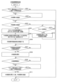
- 4 is a flowchart showing a semiconductor chip manufacturing process of the semiconductor wafer processing system according to the first embodiment.
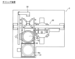
- 1 is a perspective view showing the appearance of a grooving device according to a first embodiment
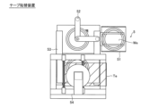
- 1 is a perspective view showing an external appearance of a dicing device according to a first embodiment
- 1 is a plan view of a dicing device according to a first embodiment.
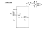
- FIG. 1 is a side view of an inner door of the dicing apparatus according to the first embodiment, as viewed from the Y1 direction.
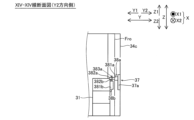
- FIG. 11 is a side view of the inner door of the dicing apparatus according to the first embodiment, as viewed from the Y2 direction.
- FIG. This is a portion on the Y1 direction side of a cross section taken along line XIV-XIV in FIG. 11 is a side view of the inner door of the dicing apparatus according to the first embodiment, as viewed from the Y2 direction.
- FIG. 1 is a side view of an inner door of the dicing apparatus according to the first embodiment, as viewed from the Y1 direction side.
- FIG. This is the Y2 side portion of the cross section taken along line XIV-XIV in FIG.
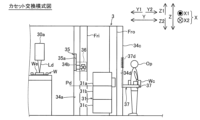
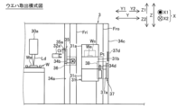
- FIG. 11 is a schematic diagram showing a state in which the outer door can be opened when the laser irradiation unit is irradiating laser during cassette replacement in the dicing device according to the first embodiment.
- FIG. 11 is a schematic diagram showing a state in which an operator is operating an operation receiving unit when a laser irradiation unit is irradiating a laser during cassette replacement in the dicing device according to the first embodiment;
- FIG. 11 is a schematic diagram showing a state in which the inner door is closed and locked while the laser irradiation unit is irradiating laser during cassette replacement in the dicing device according to the first embodiment;
- FIG. 11 is a schematic diagram showing a state in which the outer door can be opened when the laser irradiation unit is irradiating laser during cassette replacement in the dicing device according to the first embodiment.
- FIG. 11 is a schematic diagram showing a state in which the cassette unit has moved the cassette to a position where it can be replaced while the laser irradiation unit is irradiating laser during cassette replacement in the dicing device according to the first embodiment.
- FIG. 11 is a schematic diagram showing a state in which an operator operates an unlocking operation receiving unit when a laser irradiation unit is irradiating a laser during cassette replacement in the dicing device according to the first embodiment.
- FIG. 10 is a schematic diagram showing a state in which an operator opens the outer door when a laser irradiation unit is irradiating a laser during cassette replacement in the dicing device according to the first embodiment;
- FIG. 11 is a schematic diagram showing a state in which the cassette unit has moved the cassette to a position where it can be replaced while the laser irradiation unit is irradiating laser during cassette replacement in the dicing device according to the first embodiment.
- FIG. 11 is a schematic diagram showing a state in
- FIG. 11 is a schematic diagram showing a state in which an operator operates a locking operation receiving unit when changing a cassette in the dicing device according to the first embodiment, when the laser irradiation unit is irradiating a laser.
- FIG. 13 is a schematic diagram showing a state in which an operator operates the locking operation receiving unit when the laser irradiation unit is transporting a wafer by the wafer transport unit during cassette replacement in the dicing device according to the first embodiment.
- FIG. 11 is a schematic diagram showing a state in which the outer door is closed and locked while the laser irradiation unit is irradiating a laser when the wafer transport unit is removing the wafer in the dicing apparatus according to the first embodiment.
- FIG. 13 is a schematic diagram showing a state in which the cassette unit has moved to a position where the wafer can be removed while the laser irradiation unit is irradiating a laser when the wafer transport unit is removing the wafer in the dicing apparatus according to the first embodiment.
- FIG. 11 is a schematic diagram showing a state in which the inner door is open when the laser irradiation unit is irradiating a laser when the wafer transport unit removes the wafer in the dicing apparatus according to the first embodiment.
- FIG. 11 is a schematic diagram showing a state in which the inner door is open when the laser irradiation unit is irradiating a laser when the wafer transport unit removes the wafer in the dicing apparatus according to the first embodiment.
- FIG. 11 is a schematic diagram showing a state in which the clamp hand unit has removed the wafer while the laser irradiation unit is irradiating a laser when the wafer transport unit removes the wafer in the dicing apparatus according to the first embodiment.
- FIG. 10 is a flowchart showing an outer door opening and closing process in a control unit of the dicing device according to the first embodiment.
- 10 is a flowchart showing an inner door opening and closing process in a control unit of the dicing device according to the first embodiment.
- 11 is a schematic diagram showing an overview of a semiconductor wafer processing system provided with a dicing device and an expanding device according to a second embodiment.
- FIG. FIG. 11 is a plan view of a dicing device according to a second embodiment.
- 1 is a schematic diagram showing a state in which an operator opens an outer door when a transfer head unit holds a wafer during cassette replacement in the dicing apparatus according to the first embodiment;
- the semiconductor wafer processing system 100 is an apparatus for processing a wafer We.
- the semiconductor wafer processing system 100 is configured to form a modified portion on the wafer We and to divide the wafer We along the modified portion to form a plurality of semiconductor chips Ch.
- the wafer We is a circular thin plate formed of crystals of a semiconductor substance that is a material for semiconductor integrated circuits.
- a modified portion is formed by modifying the inside along a dividing line by processing in the semiconductor wafer processing system 100. That is, the wafer We is processed so as to be divisible along the dividing line.
- the modified portion refers to cracks, voids, etc. formed inside the wafer We by the laser Ld.
- the semiconductor wafer processing system 100 includes a grooving device 1, a tape application device 2, a dicing device 3, a grinding device 4, a tape replacement device 5, and an expanding device 6.
- a grooving device 1 and the dicing device 3 is an example of a "laser processing device" as defined in the claims.
- the wafer We is processed in the following order: grooving device 1, tape application device 2, dicing device 3, grinding device 4, tape replacement device 5, and expanding device 6.
- the grooving device 1 is configured to irradiate a laser Lg along the streets Ws between the semiconductor chips Ch on the circuit surface of the wafer We to which the frame Rf and the protective tape Tb are not attached, to divide the insulating film and the test pattern, before the modified portion is formed on the wafer We by the dicing device 3.
- the laser Lg is light having a wavelength shorter than that of the infrared region.
- the insulating film is an interlayer insulating film of the wafer We.
- the insulating film is formed of a low-k material having a relatively low dielectric constant as an interlayer insulating film material.
- the test pattern is a test conductive pattern for performing a function test of the semiconductor chips Ch of the wafer We.
- the test pattern is a so-called Teg (Test Element Group).
- the grooving device 1 includes a cassette unit 11, a laser irradiation unit 12, and a circuit surface coating and cleaning unit 13.
- the cassette unit 11 is configured to accommodate a wafer We to which a frame Rf and a protective tape Tb are not attached.
- the laser irradiation unit 12 is configured to irradiate a laser Lg that divides the insulating film and the test pattern of the wafer We.
- the circuit surface coating and cleaning unit 13 is configured to coat the circuit surface of the wafer We before dividing the insulating film and the test pattern, and to clean the circuit surface of the wafer We after dividing the insulating film and the test pattern.
- the cassette unit 11 is an example of a "wafer accommodation unit" in the claims.
- the tape application device 2 is configured to apply a protective tape Tb to the circuit surface of a wafer We (see FIG. 1).
- the tape application device 2 includes a cassette storage section 21, a robot hand 22, a transport mechanism 23, and a protective tape application section 24.
- the cassette storage section 21 is configured to be able to store the frame Rf, the wafer We, and the wafer We with the frame Rf.
- the robot hand 22 is configured to transport each of the frame Rf and the wafer We from the cassette storage section 21 to the transport mechanism 23.
- the robot hand 22 is configured to transport the wafer We with the frame Rf from the transport mechanism 23 to the cassette storage section 21.
- the transport mechanism 23 is configured to transport the wafer We to a position in the protective tape application section 24 where the protective tape Tb can be applied.
- the protective tape application section 24 is configured to apply the protective tape Tb to the wafer We transported by the transport mechanism 23, and to apply the frame Rf to the protective tape Tb.
- the dicing device 3 is configured to form modified portions inside the wafer We for dividing the wafer We (see FIG. 1).
- the dicing device 3 includes a dicing unit 30, a cassette unit 31, and a wafer transport unit 32.
- the dicing unit 30 is configured to form a modified portion by irradiating a laser Ld (see FIG. 1) having a wavelength that is transparent to the wafer We along the street Ws (division line).
- the laser Ld is light having a wavelength in the near-infrared region.
- the cassette unit 31 is configured to be capable of accommodating a plurality of wafers We attached to the protective tape Tb together with the frame Rf.
- the wafer transport unit 32 is configured to transport the wafers We attached to the protective tape Tb together with the frame Rf between the cassette unit 31 and the dicing unit 30.
- the cassette unit 31 is an example of a "wafer storage unit” in the claims.
- the wafer transport unit 32 is an example of a "transport unit” in the claims.
- the grinding device 4 is configured to remove the modified portion of the wafer We formed in the dicing device 3 by grinding the wafer We from the side opposite to the circuit side (see FIG. 1).
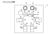
- the grinding device 4 includes a first cassette unit 41, a robot hand 42, a plurality of suction holding units 43, a plurality of grinding units 44, a finish polishing unit 45, a crystal defect forming unit 46, a second cassette unit 47, and a single rotating table unit 48.
- the first cassette unit 41 is configured to accommodate a wafer We on which a modified portion has been formed in the dicing device 3.
- the robot hand 42 is configured to transport the wafer We to which the frame Rf has been attached from the first cassette unit 41 to the suction holding unit 43 that is closest to the first cassette unit 41 among the multiple suction holding units 43.
- the robot hand 42 is also configured to transport the wafer We attached together with the frame Rf to the protective tape Tb after the modified portion has been removed from the suction holding unit 43 that is closest to the second cassette unit 47 among the multiple suction holding units 43 to the second cassette unit 47.
- the multiple suction holding units 43 are configured to suction and hold the wafer We attached together with the frame Rf to the protective tape Tb.
- the multiple grinding units 44 are configured to grind the back surface of the wafer We, which is the side opposite the circuit surface, in stages.
- the multiple grinding units 44 have a rough grinding unit 44a, a finish grinding unit 44b, and a fine grinding unit 44c.
- the rough grinding unit 44a is configured to grind the back surface of the wafer We with a first grinding material having a first particle diameter.
- the finish grinding unit 44b is configured to grind the back surface of the wafer We with a second grinding material having a second particle diameter smaller than the first particle diameter.
- the fine grinding unit 44c is configured to grind the back surface of the wafer We with a third grinding material having a third particle diameter smaller than the second particle diameter.
- the finish polishing section 45 is configured to polish the back surface of the wafer We that has been ground by the multiple grinding sections 44.
- the crystal defect forming section 46 is configured to form minute crystal defects on the back surface of the wafer We that has been ground by the finish polishing section 45.
- the crystal defect forming section 46 is configured to perform a process known as gettering.
- the second cassette section 47 is configured to accommodate the wafer We in which crystal defects have been formed in the crystal defect forming section 46.
- the single rotating table section 48 is configured to rotate and move each of the multiple suction holding sections 43 to positions corresponding to each of the multiple grinding sections 44, the finish polishing section 45, and the crystal defect forming section 46.
- the tape replacement device 5 is configured to remove the modified portion from the wafer We in the grinding device 4, and then apply the expanding tape Te to the surface of the wafer We opposite the circuit surface, and peel off the protective tape Tb applied to the circuit surface of the wafer We (see FIG. 1).
- the expanding tape Te is an example of the "sheet member" in the claims.
- the tape replacement device 5 includes a cassette storage section 51, a robot hand 52, a transport mechanism 53, an expandable tape application section 54, an ultraviolet irradiation section 55 (see FIG. 7), and a protective tape peeling section (not shown).
- the cassette storage section 51 is configured to be capable of storing a wafer We attached to a protective tape Tb together with a frame Rf, and a wafer We attached to an expansion tape Te together with a frame Rf.
- the robot hand 52 is configured to transport the wafer We attached to the protective tape Tb together with the frame Rf from the cassette storage section 51 to the transport mechanism 53.
- the transport mechanism 53 is configured to transport the wafer We attached to the protective tape Tb together with the frame Rf to the expansion tape application section 54.
- the expansion tape application section 54 is configured to apply the expansion tape Te to the surface of the frame Rf opposite to the surface to which the protective tape Tb is applied, thereby applying the frame Rf and the wafer We to each of the protective tape Tb and the expansion tape Te.
- the robot hand 52 is configured to carry the wafer We attached to each of the protective tape Tb and the expanding tape Te together with the frame Rf from the transport mechanism 53 to the ultraviolet irradiation unit 55.
- the ultraviolet irradiation unit 55 is located inside an airtight structure with a door at the entrance and exit, and is configured to remove oxygen from the atmosphere by nitrogen purging and fill the inside with nitrogen (nitrogen is supplied to the inside and nitrogen is filled while oxygen is discharged), and then irradiate ultraviolet rays toward the surface of the frame Rf to which the protective tape Tb is attached. This hardens the adhesive layer of the protective tape Tb.
- the robot hand 52 is configured to return the wafer We attached to each of the protective tape Tb and the expanding tape Te together with the frame Rf from the ultraviolet irradiation unit 55 to the transport mechanism 53.
- the transport mechanism 53 is configured to transport the wafer We attached to each of the protective tape Tb and the expanding tape Te together with the frame Rf to the protective tape peeling section.
- the protective tape peeling section is configured to peel off the protective tape Tb (see FIG. 1).
- the robot hand 52 is configured to store the wafer We attached to the expanding tape Te together with the frame Rf from the transport mechanism 53 in the cassette storage section 51.
- the expanding device 6 is configured to attach an expanding tape Te to the surface of the wafer We opposite the circuit surface, and then expand the expanding tape Te to divide the wafer We into a plurality of semiconductor chips Ch (see FIG. 1).
- the expansion device 6 includes a cassette section 601, a lift-up hand section 602, a suction hand section 603, a cold air supply section 604 (see Figure 9), a cooling unit 605, an expansion section 606, an expansion maintaining member 607, a heat shrink section 608 (see Figure 9), an ultraviolet ray irradiation section 609 (see Figure 9), a squeegee section 610, and a clamp section 611.
- the cassette section 601 is configured to be capable of housing a wafer ring structure W in which a frame Rf and a wafer We are attached to an expanding tape Te.
- the lift-up hand section 602 is configured to be capable of removing the wafer ring structure W from the cassette section 601.
- the lift-up hand section 602 is configured to be capable of housing the wafer ring structure W in the cassette section 601.
- the suction hand section 603 is configured to suction the frame Rf of the wafer ring structure W from above.
- the cold air supply section 604 is configured to supply cold air from above to the expanding tape Te when the expanding section 606 expands the expanding tape Te.
- the cooling unit 605 is configured to cool the expanding tape Te from below.
- the expanding section 606 is configured to expand the expanding tape Te of the wafer ring structure W, thereby dividing the wafer We along the streets Ws (see FIG. 1).
- the expansion maintaining member 607 is configured to press the expanding tape Te from above so that the expanding tape Te near the wafer We does not shrink due to heating by the heat shrink section 608.
- the heat shrink section 608 is configured to heat and shrink the expanding tape Te expanded by the expanding section 606 while maintaining the gaps between the multiple semiconductor chips Ch.
- the ultraviolet ray irradiation section 609 is configured to irradiate the expanding tape Te with ultraviolet rays in order to reduce the adhesive strength of the adhesive layer of the expanding tape Te.
- the squeegee unit 610 is configured to expand the expanding tape Te and then locally press the wafer We from below to further divide the wafer We along the modified portion.
- the clamp unit 611 is configured to be able to move the wafer ring structure W in the vertical direction while gripping the frame Rf of the wafer ring structure W.
- the clamp unit 611 is configured to be able to move the wafer ring structure W in both directions from the cooling unit 605 toward the expanding unit 606 and from the expanding unit 606 toward the cooling unit 605 while gripping the frame Rf of the wafer ring structure W.
- step S1 the insulating film and the test pattern are divided in the grooving device 1. That is, the laser irradiation unit 12 irradiates the laser Lg along the streets Ws between the semiconductor chips Ch on the circuit surface of the wafer We that are not attached to the protective tape Tb together with the frame Rf to divide the insulating film and the test pattern.
- step S2 the wafer We and the frame Rf are attached to the protective tape Tb in the tape attachment device 2. That is, the protective tape attachment unit 24 attaches the protective tape Tb to the wafer We transported by the transport mechanism 23, and also attaches the frame Rf to the protective tape Tb.
- step S3 a modified portion is formed on the wafer We in the dicing device 3. That is, the dicing unit 30 forms the modified portion by irradiating the wafer We with a laser Ld (see FIG. 1) along the streets Ws.
- step S4 the modified portion is removed from the wafer We in the grinding device 4. That is, the multiple grinding units 44 remove the modified portion of the wafer We by gradually grinding the back surface of the wafer We opposite the circuit surface.
- step S5 the tape replacement unit 5 peels off the protective tape Tb and attaches the wafer We and the frame Rf to the expandable tape Te.
- the expandable tape attachment unit 54 peels off the protective tape Tb from the wafer We with the frame Rf, and then attaches the expandable tape Te to the wafer We from which the protective tape Tb has been peeled off, and attaches the frame Rf to the expandable tape Te.
- step S6 the expanding tape Te is expanded in the expanding device 6 to divide the wafer We into multiple semiconductor chips Ch. That is, the clamping section 611 descends while holding the frame Rf, and the expanding tape Te in contact with the expanding section 606 is pulled downward, causing the expanding tape Te to expand. As a result, the expanding tape Te is divided along the cracks formed in the streets Ws of the wafer We by the tensile force generated in the expanding tape Te as a result of the expansion, and the wafer We is divided into multiple semiconductor chips Ch.
- step S6 the semiconductor chip manufacturing process ends.
- the wafer We is processed by the laser Lg emitted from the laser irradiation unit 12.
- an operator Op performs an exchange operation of supplying the wafer We before processing and removing the wafer We after processing.
- supplying the wafer We before processing means that the operator Op carries a cassette Wc on which a plurality of wafers We are placed, and places the cassette Wc at a predetermined position in the cassette unit 11.
- removing the wafer We after processing means that the operator Op takes the cassette Wc placed at a predetermined position in the cassette unit 11 out of the device and carries it to another location.
- the grooving device 1 of the first embodiment includes an apparatus cover section 14, an inner door 15, an outer door 16, and a control section 17 to prevent leakage of the laser Lg.
- the apparatus cover section 14 is configured to accommodate the cassette section 11, the transport section (not shown), and the laser irradiation section 12 therein.
- the inner door 15 is provided on the inner wall section 14a of the apparatus cover section 14 on the laser irradiation section 12 side of the cassette section 11, and is configured to open when the transport section takes out and stores the wafer We.
- the outer door 16 is provided on the outer wall section 14b of the apparatus cover section 14 on the opposite side to the laser irradiation section 12 side of the cassette section 11, and is configured to open when the operator Op takes out and stores the wafer We.
- the control unit 17 is configured to control the inner door 15 to remain closed when the outer door 16 is made openable. As a result, when the worker Op opens the outer door 16 to perform replacement work, the inner door 15 is closed, so the laser Lg irradiated from the laser irradiation unit 12 does not leak outside the device.
- the wafer We is processed by the laser Ld irradiated from the laser irradiation unit 30a. For this reason, the worker Op performs replacement work by supplying the wafer We before processing and removing the wafer We after processing.
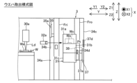
- the dicing device 3 of the first embodiment includes an apparatus cover section 34, an inner door 35, an outer door 37, and a control section 39 to prevent leakage of the laser Ld.
- the apparatus cover section 34 is configured to house the dicing section 30, the cassette section 31, the wafer transport section 32, and the control section 39.
- the inner door 35 is provided on the inner wall section 34a of the apparatus cover section 34 on the laser irradiation section 30a side of the cassette section 31, and is configured to open when the wafer We is taken out and stored by the wafer transport section 32.
- the outer door 37 is provided on the outer wall section 34c of the apparatus cover section 34 on the opposite side to the laser irradiation section 30a side of the cassette section 31, and is configured to open when the operator Op takes out and stores the wafer We.
- the control unit 39 is configured to control the inner door 35 to remain closed when the outer door 37 is made openable. As a result, when the worker Op opens the outer door 37 to perform replacement work, the inner door 35 is closed, so that the laser Ld irradiated from the laser irradiation unit 30a does not leak outside the device.
- the dicing apparatus 3 includes a dicing section 30, a cassette section 31, a wafer transport section 32, a base section 33, an apparatus cover section 34, an inner door 35, an inner door locking section 36, an outer door 37, an outer door locking section 38, and a control section 39.
- the up-down direction is the Z direction
- the up direction is the Z1 direction
- the down direction is the Z2 direction.
- the horizontal direction perpendicular to the Z direction is the X direction
- one side of the X direction is the X1 direction
- the other side of the X direction is the X2 direction.
- the horizontal direction perpendicular to the X direction is the Y direction
- one side of the Y direction is the Y1 direction
- the other side of the Y direction is the Y2 direction.
- the dicing section 30 includes a laser irradiation section 30a, a chuck table section 30b, an imaging section 30c, and an imaging section 30d.
- the laser irradiation unit 30a is configured to irradiate the laser Ld along each of the multiple streets Ws of the wafer We that is taken out of the cassette unit 31 and supplied by the wafer transport unit 32. Specifically, the laser irradiation unit 30a is configured to irradiate the laser Ld along each of the multiple streets Ws of the wafer We while moving the wafer We relative to the laser irradiation unit 30a by the chuck table unit 30b.
- the direction extending along each of the multiple streets Ws of the wafer We is the processing direction.
- the processing direction is the X1 direction or the X2 direction.
- the chuck table portion 30b is configured to hold the wafer We by adsorbing the frame Rf attached to the protective tape Tb.
- the chuck table portion 30b is configured to rotate or move horizontally while adsorbing the frame Rf.
- the chuck table portion 30b has a rotation portion 301b, a Y-direction movement portion 302b, and an X-direction movement portion 303b.
- Each of the imaging units 30c and 30d is configured to capture an image of the wafer We held on the chuck table unit 30b.
- Each of the imaging units 30c and 30d is a near-infrared imaging camera.
- Each of the imaging units 30c and 30d is movable in the Z1 direction or the Z2 direction.
- the cassette unit 31 is configured to be able to accommodate a plurality of cassettes Wc, each of which has a plurality of wafer ring structures W, each of which is made up of a wafer We attached to a protective tape Tb and a frame Rf.
- the cassette unit 31 includes a first cassette mounting portion 31a, a second cassette mounting portion 31b, a third cassette mounting portion 31c, and a Z-direction movement mechanism 31d.
- a cassette Wc containing multiple unprocessed wafers We is placed on each of the first cassette placing section 31a and the second cassette placing section 31b by an operator Op.
- a cassette Wc containing multiple processed wafers We is placed on each of the first cassette placing section 31a and the second cassette placing section 31b by the wafer transport section 32.
- the operator Op removes the cassette Wc containing multiple processed wafers We from each of the first cassette placing section 31a and the second cassette placing section 31b.
- a cassette Wc containing multiple processed wafers We is placed on the third cassette placing section 31c by the wafer transport section 32.
- a quality manager removes the cassette Wc containing multiple processed wafers We from the third cassette placing section 31c. That is, the processed wafers We in the cassette Wc placed on the third cassette placement section 31c are wafers We for periodic inspection.
- the quality control officer is an example of the "operator" in the claims.
- the Z-direction movement mechanism 31d is configured to move the first cassette loading section 31a, the second cassette loading section 31b, and the third cassette loading section 31c together in the Z1 direction or the Z2 direction.
- the Z-direction movement mechanism 31d has, for example, a linear conveyor module or a drive section having a ball screw and a motor with an encoder.
- the wafer transport unit 32 is configured to transport the wafer ring structure W between the cassette unit 31 and the dicing unit 30. Specifically, the wafer transport unit 32 has a clamp hand unit 32a, a Y-direction movement mechanism 32b, a rail unit 32c, a rail unit 32d, a suction hand unit 32e, and a Z-direction movement mechanism 32f.
- the clamp hand portion 32a is configured to clamp the frame Rf of the wafer ring structure W and remove it from the cassette portion 31 or store it in the cassette portion 31.
- the clamp hand portion 32a has a clamp portion 321a at its tip that clamps the frame Rf of the wafer ring structure W.
- the clamp portion 321a is configured to clamp the end portion of the frame Rf of the wafer ring structure W on the Y1 direction side in the vertical direction.
- the clamp hand unit 32a is moved in the Y1 or Y2 direction by the Y-direction movement mechanism 32b.
- the clamp hand unit 32a transports the wafer ring structure W by being moved by the Y-direction movement mechanism 32b.
- the Y-direction movement mechanism 32b has, for example, a linear conveyor module or a drive unit having a ball screw and a motor with an encoder.
- the clamp hand unit 32a transports the wafer ring structure W removed from the cassette unit 31 to the rail unit 32c using the Y-direction movement mechanism 32b.
- the clamp hand unit 32a transports the wafer ring structure W transported to the rail unit 32c to the rail unit 32d using the Y-direction movement mechanism 32b.
- the clamp hand unit 32a stores the processed wafer ring structure W placed on the rail unit 32d in the cassette unit 31 using the Y-direction movement mechanism 32b.
- Rail portion 32c is configured to support the wafer ring structure W placed by clamp hand portion 32a from the Z2 direction side.
- Rail portion 32d is configured to support the wafer ring structure W placed by either clamp hand portion 32a or suction hand portion 32e from the Z2 direction side.
- Rail portion 32c and rail portion 32d are arranged side by side in this order from the Y2 direction side toward the Y1 direction side.
- Rail portion 32c is arranged near cassette portion 31.
- Rail portion 32d is arranged near rail portion 32c.
- the suction hand part 32e is configured to suction the frame Rf of the wafer ring structure W.
- the suction hand part 32e is provided with suction holes and the like for suctioning the frame Rf of the wafer ring structure W.
- the Z-direction movement mechanism 32f is configured to move the suction hand part 32e in the Z1 direction or the Z2 direction.
- the Z-direction movement mechanism 32f has, for example, a linear conveyor module or a drive part having a ball screw and a motor with an encoder.
- the dicing section 30 and the wafer transport section 32 are installed on the base section 33.
- the equipment cover section 34 covers the dicing section 30, the cassette section 31, the wafer transport section 32, the base section 33, and the control section 39.
- Such an equipment cover section 34 has an inner wall section 34a, an inner door opening 34b, an outer wall section 34c, and an outer door opening 34d.
- the inner wall 34a is a partition wall of the device cover 34 that separates the cassette 31 from the laser irradiation unit 30a. That is, the inner wall 34a separates the cassette 31 from the laser irradiation unit 30a in the space inside the device cover 34.
- the inner door opening 34b connects the space on the cassette 31 side to the space of the laser irradiation unit 30a in the space inside the device cover 34.
- the inner door opening 34b is a through hole that penetrates the inner wall 34a in the Y direction, and is located at a height position on the Z1 direction side of the outer door opening 34d.
- the outer wall portion 34c is a wall of the device cover portion 34 on the opposite side (Y2 direction side) from the laser irradiation portion 30a side relative to the inner wall portion 34a.
- the outer wall portion 34c is one of the partition walls of the device cover portion 34 provided between the space inside the device cover portion 34 and the external space.
- the outer door opening 34d connects the space on the cassette portion 31 side in the space inside the device cover portion 34 with the external space of the device cover portion 34.
- the outer door opening 34d is a through hole that penetrates the outer wall portion 34c in the Y direction, and is located at a height position on the Z2 direction side of the inner door opening 34b.
- the inner door 35 is an inner door of a double door provided to block the laser Ld irradiated from the laser irradiation unit 30a.
- Fig. 14 is a view of the inner wall portion 34a on which the inner door 35 is provided, seen from the Y1 direction side.
- the inner door 35 is configured to open when the wafer transfer unit 32 takes out and stores the wafer ring structure W (wafer We).
- the inner door 35 has a door body 35a, a moving part 35b, an opening/closing detection sensor 35c, and a wafer detection sensor 35d (see Figure 15).
- the door body 35a is configured to close the inner door opening 34b. In both the X and Z directions, the dimensions of the door body 35a are larger than the dimensions of the inner door opening 34b.
- the moving unit 35b is configured to move the door body 35a in the opening and closing direction.
- the moving unit 35b is configured with a linear movement mechanism that moves the door body 35a in the Ci direction (closing direction) or the Oi direction (opening direction).
- the Oi direction is a direction parallel to the Z1 direction
- the Ci direction is a direction parallel to the Z2 direction.
- the moving unit 35b has a solenoid 351b, a guide rail 352b, and a movement detection sensor (not shown).
- the movement detection sensor is a sensor that detects the movement of the plunger of the solenoid 351b in either the Z1 direction or the Z2 direction.
- the opening/closing detection sensor 35c is a sensor that detects the opening or closing of the inner door opening 34b by the door body 35a of the inner door 35.
- the opening/closing detection sensor 35c is a magnetic sensor that has a magnetic field generating unit 351c and a magnetic field detecting unit 352c.
- the opening/closing detection sensor 35c may be a sensor that uses another detection method.
- the magnetic field generating unit 351c and the magnetic field detecting unit 352c come close to each other, and the magnetic field detecting unit 352c detects the magnetic field generated by the magnetic field generating unit 351c.
- the opening/closing detection sensor 35c detects the closing of the inner door opening 34b by the door body 35a of the inner door 35.
- the magnetic field generating unit 351c and the magnetic field detecting unit 352c come apart, and the magnetic field detecting unit 352c cannot detect the magnetic field generated by the magnetic field generating unit 351c.
- the opening/closing detection sensor 35c detects the opening of the inner door opening 34b by the door body 35a of the inner door 35.
- the wafer detection sensor 35d is a sensor that detects the passage of the wafer ring structure W transported by the clamp hand portion 32a through the inner door opening 34b.
- the wafer detection sensor 35d is a transmission type sensor having a light projecting portion 351d and a light receiving portion 353d. Note that the wafer detection sensor 35d may be a sensor that uses another detection method.
- the inner door locking portion 36 is configured to lock the inner door 35.
- the inner door locking portion 36 has an inner door locking engaging portion 36a and an inner door locking engaged portion 36b.
- the inner door locking engaging portion 36a is configured to engage with the inner door locking engaged portion 36b.
- the inner door locking engaging portion 36a is attached to the surface on the Y2 direction side of the door body 35a of the inner door 35.
- the inner door locking engaging portion 36a has a storage portion 361a and a protruding rod portion 362a.
- the storage portion 361a stores the protruding rod portion 362a so that it can move forward and backward.
- the protruding rod portion 362a protrudes from the storage portion 361a by moving in the Y2 direction.
- the protruding rod portion 362a is stored in the storage portion 361a by moving in the Y1 direction.
- the protruding rod portion 362a is formed with a through hole 363a that penetrates in the X direction.
- the inner door locking engaged part 36b is configured to engage with the inner door locking engaging part 36a.
- the inner door locking engaged part 36b is attached to the frame Fri that supports the device cover part 34.
- the inner door locking engaged part 36b has a storage part 361b and a protruding rod part 362b.
- the storage part 361b stores the protruding rod part 362b so that it can move forward and backward.
- the protruding rod part 362b protrudes from the storage part 361b by moving in the X1 direction.
- the protruding rod part 362b is stored in the storage part 361b by moving in the X2 direction.
- the inner door locking section 36 locks the inner door 35 by inserting the protruding rod section 362b into the through hole 363a of the protruding rod section 362a.
- the outer door 37 is the outer door of a double door provided to block the laser Ld irradiated from the laser irradiation unit 30a.
- Fig. 17 is a view of the outer wall portion 34c on which the outer door 37 is provided, viewed from the Y2 direction side.
- the outer door 37 is configured to be manually moved in the opening and closing directions by an operator Op.
- the opening direction of the opening and closing directions is the Oo direction
- the closing direction of the opening and closing directions is the Co direction.
- the outer door 37 has a door body 37a, a handle portion 37b, an opening/closing detection sensor 37c, and an operation receiving portion 37d.
- the door body 37a is configured to close the exterior door opening 34d. In both the X and Z directions, the dimensions of the door body 37a are approximately the same as the dimensions of the exterior door opening 34d.
- the handle portion 37b is configured to move the door body 37a in the opening and closing direction.
- the handle portion 37b is a member for rotating the door body 37a in the Oo direction (opening direction) when pulled in the Y2 direction by the operator Op.
- the handle portion 37b is a member for rotating the door body 37a in the Co direction (closing direction) when pushed in the Y1 direction by the operator Op.
- the magnetic field generating unit 371c and the magnetic field detecting unit 372c come close to each other, and the magnetic field detecting unit 372c detects the magnetic field generated by the magnetic field generating unit 371c.
- the opening/closing detection sensor 37c detects the closing of the exterior door opening 34d by the door body 37a of the exterior door 37.
- the magnetic field generating unit 371c and the magnetic field detecting unit 372c come apart, and the magnetic field detecting unit 372c cannot detect the magnetic field generated by the magnetic field generating unit 371c.
- the opening/closing detection sensor 37c detects the opening of the exterior door opening 34d by the door body 37a of the exterior door 37.
- the operation reception unit 37d is configured to receive operations from the operator Op.
- the operation reception unit 37d has an unlock operation reception unit 371d, a third cassette exchange request unit 372d, a first cassette exchange request unit 373d, a second cassette exchange request unit 374d, and a lock operation reception unit 375d.
- Each of the unlock operation reception unit 371d, the third cassette exchange request unit 372d, the first cassette exchange request unit 373d, the second cassette exchange request unit 374d, and the lock operation reception unit 375d is a plurality of (five) push buttons arranged in a row from the Z1 direction side to the Z2 direction side. The number of push buttons may be one to four, or six or more.
- the unlocking operation reception unit 371d is configured to be able to receive an operation (pressing operation) by the worker Op.
- the unlocking operation reception unit 371d is configured to transmit a signal to the control unit 39 to unlock the outer door 37 locked by the outer door locking unit 38 based on receiving an operation by the worker Op.
- the unlocking operation reception unit 371d is normally lit.
- the unlocking operation reception unit 371d is configured to flash when preparations to open the outer door 37 are complete after any of the first cassette exchange request unit 373d, the second cassette exchange request unit 374d, and the third cassette exchange request unit 372d receives an operation by the worker Op.
- the unlocking operation reception unit 371d goes out when the outer door 37 is opened by the worker Op.
- the unlocking operation receiving section 371d is configured to light up when the locking operation receiving section 375d is operated by the worker Op to lock the outer door 37.
- the third cassette exchange request unit 372d is configured to be able to accept an operation (pressing operation) by a quality manager.
- the quality manager operates the third cassette exchange request unit 372d to periodically perform visual inspection of the wafer We.
- the third cassette exchange request unit 372d is configured to transmit a signal to the control unit 39 requesting that the third cassette placement unit 31c be moved to the removal position (Pd position in FIG. 23).
- the third cassette exchange request unit 372d is lit if the third cassette placement unit 31c can store the cassette Wc.
- the third cassette exchange request unit 372d is turned off if there is no cassette Wc in the third cassette placement unit 31c. If the third cassette placement unit 31c is fully loaded with cassettes Wc, the third cassette exchange request unit 372d flashes to indicate that the cassette Wc needs to be removed.
- the third cassette exchange request unit 372d starts flashing rapidly based on receiving an operation by the quality manager, and transmits a signal to the control unit 39 requesting that the third cassette placement unit 31c be moved to the removal position.
- the third cassette exchange request unit 372d is configured to stop flashing rapidly and return to normal lighting based on the outer door 37 being locked by the quality manager operating the lock operation receiving unit 375d.
- the first cassette exchange request unit 373d is configured to be able to accept an operation by the operator Op.
- the operator Op operates the first cassette exchange request unit 373d to exchange the cassette Wc placed on the first cassette loading unit 31a.
- the first cassette exchange request unit 373d is configured to transmit a signal to the control unit 39 requesting that the first cassette loading unit 31a be moved to the removal position (Pd position in FIG. 23) based on the acceptance of an operation by the operator Op.
- the first cassette exchange request unit 373d is lit if the first cassette placement unit 31a can store the cassette Wc.
- the first cassette exchange request unit 373d is turned off if there is no cassette Wc on the first cassette placement unit 31a. If the first cassette placement unit 31a is full of processed cassettes Wc, the first cassette exchange request unit 373d flashes to indicate that the cassette Wc needs to be removed.
- the first cassette exchange request unit 373d starts flashing rapidly based on receiving an operation by the operator Op, and transmits a signal to the control unit 39 requesting that the first cassette placement unit 31a be moved to the removal position.
- the first cassette exchange request unit 373d is configured to stop flashing rapidly and return to normal lighting based on the outer door 37 being locked by the operator Op operating the lock operation receiving unit 375d.
- the second cassette exchange request unit 374d is configured to be able to accept an operation by the operator Op.
- the operator Op operates the second cassette exchange request unit 374d to exchange the cassette Wc placed on the second cassette loading unit 31b.
- the second cassette exchange request unit 374d is configured to transmit a signal to the control unit 39 requesting that the second cassette loading unit 31b be moved to the removal position (Pd position in FIG. 23) based on the acceptance of an operation by the operator Op.
- the second cassette exchange request unit 374d is lit if the second cassette placement unit 31b can store the cassette Wc.
- the second cassette exchange request unit 374d is turned off if there is no cassette Wc on the second cassette placement unit 31b. If the second cassette placement unit 31b is full of processed cassettes Wc, the second cassette exchange request unit 374d flashes to notify the user that the cassette Wc needs to be removed.
- the second cassette exchange request unit 374d starts flashing rapidly based on the receipt of an operation by the operator Op, and transmits a signal to the control unit 39 requesting that the second cassette placement unit 31b be moved to the removal position.
- the second cassette exchange request unit 374d is configured to stop flashing rapidly and return to normal lighting based on the lock operation receipt unit 375d being operated by the operator Op to lock the outer door 37.
- the locking reception unit 365d is configured to be able to receive an operation by the worker Op.
- the locking reception unit 365d is configured to transmit a signal to the control unit 39 to lock the outer door 37 by the outer door locking unit 38 based on receiving an operation by the worker Op.
- the locking operation reception unit 375d is normally lit.
- the locking operation reception unit 375d flashes when the outer door 37 is opened by the worker Op.
- the locking operation reception unit 375d is configured to transmit a signal to lock the outer door 37 to the control unit 39 based on the operation of the locking operation reception unit 375d by the worker Op after the outer door 37 is closed by the worker Op.
- the locking operation reception unit 375d is configured to return to normal lighting after the outer door 37 is locked by the worker Op.
- the outer door locking portion 38 is configured to lock the outer door 37.
- the outer door locking portion 38 has an outer door locking engaging portion 38a and an outer door locking engaged portion 38b.
- the outer door locking engaging portion 38a is configured to engage with the outer door locking engaged portion 38b.
- the outer door locking engaging portion 38a is attached to the surface on the Y1 direction side of the door body 37a of the outer door 37.
- the outer door locking engaging portion 38a has a storage portion 381a and a protruding rod portion 382a.
- the storage portion 381a stores the protruding rod portion 382a so that it can move forward and backward.
- the protruding rod portion 382a protrudes from the storage portion 381a by moving in the Y1 direction.
- the protruding rod portion 382a is stored in the storage portion 381a by moving in the Y1 direction.
- the protruding rod portion 382a is formed with a through hole 383a that penetrates in the Z direction.
- the outer door locking engaged part 38b is configured to engage with the outer door locking engaging part 38a.
- the outer door locking engaged part 38b is attached to the frame Fro that supports the device cover part 34.
- the outer door locking engaged part 38b has a storage part 381b and a protruding rod part 382b.
- the storage part 381b stores the protruding rod part 382b so that it can move forward and backward.
- the protruding rod part 382b protrudes from the storage part 381b by moving in the Z1 direction.
- the protruding rod part 382b is stored in the storage part 381b by moving in the Z2 direction.
- the outer door locking section 38 locks the outer door 37 by inserting the protruding rod section 382b into the through hole 383a of the protruding rod section 382a.
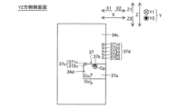
- the control unit 39 is configured to control each of the dicing unit 30, the cassette unit 31, the wafer transport unit 32, the inner door 35, the inner door locking unit 36, and the outer door locking unit 38 in order to process the wafer We in the dicing device 3.
- the control unit 39 is electrically connected to each of the dicing unit 30, the cassette unit 31, the wafer transport unit 32, the inner door 35, the inner door locking unit 36, the outer door 37, and the outer door locking unit 38.
- control unit 39 includes a CPU (Central Processing Unit) and a storage unit having a ROM (Read Only Memory), a RAM (Random Access Memory), an SSD (Solid State Drive), etc.
- the storage unit stores a control program that controls the dicing device 3.
- the control unit 39 in the first embodiment is configured to control the opening and closing of the double door so that an operator Op (quality maintainer) can at least either remove a cassette Wc from the cassette unit 31 or store a new cassette Wc in the cassette unit 31 while the laser irradiation unit 30a is irradiating the laser Ld.
- Figs. 20 to 26 show an example of a cassette exchange by the operator Op.
- cassette exchange refers to removing a cassette Wc from the cassette unit 31 and then storing a new cassette Wc in the cassette unit 31.
- control unit 39 is configured to perform control to maintain the inner door 35 closed when the outer door 37 is made openable.
- control unit 39 is configured to perform control to maintain the inner door 35 closed when the outer door 37 is made openable while the laser irradiation unit 30a is irradiating the laser Ld.
- the control unit 39 is configured to perform control to make the outer door 37 openable after detecting that the inner door 35 is closed.
- control configuration for making the outer door 37 openable will be explained using an example of an operator Op replacing a cassette Wc.
- an example is shown of a situation in which an operator Op replaces a cassette Wc placed on the first cassette placement section 31a while a wafer We is being processed by a laser Ld irradiated from the laser irradiation section 30a.
- control for making the outer door 37 openable is also performed when the operator Op replaces a cassette Wc placed on the second cassette placement section 31b, and when a quality control person replaces a cassette Wc placed on the third cassette placement section 31c.
- control unit 39 judges whether or not it is possible to start the process for making the outer door 37 openable. This judgment will be described below.
- the control unit 39 is configured to perform control to determine whether or not there is a wafer We (wafer We being processed) currently being processed by the laser irradiation unit 30a among the multiple wafers We in the cassette Wc placed on the first cassette placement unit 31a, based on the acquisition (reception) of a signal by the operator Op to operate the first cassette exchange request unit 373d.
- the first cassette exchange request unit 373d designated by the operator Op is the target cassette Wc designated by the operator Op.
- the wafer We being processed is a wafer We that has been transported from the target cassette Wc to the laser irradiation unit 20a and is being processed by the laser Ld.
- Information such as the position of each of the multiple wafers We in the cassette Wc is stored in advance in an external server or the like.
- control unit 39 determines that there is no wafer We currently being processed by the laser irradiation unit 30a in the target cassette Wc, the control unit 39 is configured to perform control to determine whether or not there is a wafer We (unprocessed wafer We) that has not been processed by the laser irradiation unit 30a among the multiple corresponding wafers We in the cassette Wc (target cassette Wc) placed on the first cassette placement unit 31a.
- the control unit 39 determines that there is a wafer We that has not been processed by the laser irradiation unit 30a
- the control unit 39 is configured to perform control to display a screen that accepts the decision of whether or not to change the cassette from the operator Op.
- control unit 39 When the control unit 39 receives a decision from the operator Op not to change the cassette, the control unit 39 is configured to end the control. When the control unit 39 receives a decision from the operator Op to change the cassette, the control unit 39 is configured to perform control to determine whether or not there is a wafer We that has not been stored in the cassette unit 31 described later.
- control unit 39 determines that there is no wafer We that has not been processed by the laser irradiation unit 30a, it is configured to perform control to determine whether or not there is a wafer We being transported by the wafer transport unit 32 among the multiple corresponding wafers We in the cassette Wc (target cassette Wc) placed on the first cassette placement unit 31a.
- the control unit 39 is configured to perform control to determine the locking state of each of the inner door 35 and the outer door 37 described below.
- the control unit 39 is configured to perform control to wait until the wafer We being transported is stored in the cassette Wc placed on the first cassette placement unit 31a by the clamp hand unit 32a of the wafer transport unit 32.
- the control unit 39 judges whether or not it is possible to start the process of making the outer door 37 openable. If the result of this judgment is that it is possible to start the process of making the outer door 37 openable, the control unit 39 starts the process of making the outer door 37 openable. If the result of this judgment is that it is not possible to start the process, the control in the control unit 39 ends.
- control unit 39 is configured to start a process to make the outer door 37 openable based on the fact that the inner door 35 is closed and locked by the inner door locking unit 36.
- the control unit 39 when the inner door 35 is open, the control unit 39 is configured to control the movement unit 35b to move the inner door 35 in the Ci direction (closing direction), and after detecting that the inner door 35 is closed, to make the outer door 37 openable.
- the control unit 39 when the opening/closing detection sensor 35c detects that the door body 35a is open, the control unit 39 is configured to control the movement unit 35b to move the door body 35a in the Ci direction.
- the control unit 39 is configured to control the inner door locking unit 36 to lock the inner door 35 based on the opening/closing detection sensor 35c detecting that the door body 35a is closed.
- the control unit 39 is configured to control the outer door 37 to be openable after detecting that the inner door 35 is locked by the inner door locking unit 36.
- the control unit 39 is also configured to control the start of a process to make the outer door 37 openable based on the outer door 37 being closed and locked by the outer door locking unit 38.
- the control unit 39 when the outer door 37 is open, the control unit 39 is configured to detect that the outer door 37 has been closed by the worker Op, and then control the outer door 37 to be in an openable state. Specifically, the control unit 39 is configured to control the outer door locking unit 38 to lock the outer door 37 based on the detection by the open/close detection sensor 37c that the door body 37a has been closed. The control unit 39 is configured to control the outer door 37 to be in an openable state, after detecting that the outer door 37 has been locked by the outer door locking unit 38.
- control unit 39 is configured to control the Z-direction movement mechanism 31d to move the cassette Wc in the cassette unit 31, on which the wafer We that has been requested to be replaced by the operator Op, to the Pd position where it can be replaced, based on the inner door 35 being closed and locked by the inner door locking unit 36, and the outer door 37 being closed and locked by the outer door locking unit 38. Note that, as an example, in FIG. 23, the cassette Wc placed on the first cassette placement unit 31a is moved to the Pd position.
- control unit 39 is configured not to perform processing to make the outer door 37 openable unless the inner door 35 is closed and locked by the inner door locking unit 36, and the outer door 37 is closed and locked by the outer door locking unit 38. In this case, control in the control unit 39 ends.
- the control unit 39 is configured to set the inner door 35 not to accept a signal to open it based on the fact that the cassette Wc has been moved to the Pd position where it can be replaced, and to control the outer door 37 to be unlocked by the outer door locking unit 38.
- the setting of not accepting a signal to open the inner door 35 refers to a setting in the control unit 39 not to accept a signal requesting the opening of the inner door 35 sent from the dicing unit 30, cassette unit 31, wafer transport unit 32, etc.
- the control unit 39 is configured to perform control to unlock the outer door 37 and make the outer door 37 openable based on receipt of a signal to unlock the outer door 37 from the unlocking operation receiving unit 371d.
- the state where the outer door 37 can be unlocked is notified to the operator Op by flashing the unlocking operation receiving unit 371d based on a signal from the control unit 39.
- control unit 39 is configured to perform control to cause the unlocking operation receiving unit 371d to flash when the outer door 37 can be unlocked.
- the control unit 39 is configured to perform control to unlock the outer door 37 and make the outer door 37 openable based on receipt of a signal to unlock the outer door 37 transmitted from the unlocking operation receiving unit 371d by the operation of the worker Op.
- the above control allows the worker Op to open the outer door 37, as shown in FIG. 25. At this time, the inner door 35 is locked by the inner door locking unit 36. After opening the outer door 37, the worker Op removes the cassette Wc from the first cassette loading unit 31a, and then places a new cassette Wc on the first cassette loading unit 31a. Then, the worker Op closes the outer door 37, and presses the locking operation receiving unit 375d.
- the control unit 39 is configured to control the unlocking operation reception unit 371d to be turned off and the locking operation reception unit 375d to be flashing based on the opening/closing detection sensor 37c detecting that the outer door 37 has been opened by the worker Op.
- the control unit 39 is configured to control the unlocking operation reception unit 371d to be normally lit and the locking operation reception unit 375d to be normally lit based on the opening/closing detection sensor 37c detecting that the outer door 37 has been closed by the worker Op.
- the control unit 39 is also configured to control the cassette unit 31 to be returned to its original position.
- the above-mentioned control process makes the outer door 37 openable.
- an operator Op quality holder
- an operator Op quality holder
- an operator Op at least either removes a cassette Wc from the cassette section 31 or stores a new cassette Wc in the cassette section 31 while the laser Ld is being irradiated from the laser irradiation section 30a.
- an operator Op quality holder
- an operator Op at least either removes a cassette Wc from the cassette section 31 or stores a new cassette Wc in the cassette section 31 while the clamp hand section 32a of the wafer transport section 32 is transporting a wafer We.
- the control unit 39 of the first embodiment is configured to control the clamp hand unit 32a of the wafer transport unit 32 to take out and store the wafer We when an operator Op (quality holder) has not taken out the cassette Wc from the cassette unit 31 or stored a new cassette Wc in the cassette unit 31.
- FIGS. 28 to 31 diagrammatically show an example of how the clamp hand unit 32a takes out the wafer We from the cassette Wc.
- control unit 39 when the inner door 35 is opened, the control unit 39 is configured to perform control to keep the outer door 37 closed. At this time, when the outer door 37 is open because the operator Op has removed and stored the wafer We, the control unit 39 is configured to perform control to open the inner door 35 after detecting that the outer door 37 has been closed.
- control configuration for opening the inner door 35 is shown as an example of a situation in which the clamp hand unit 32a is removing the wafer We. Note that the same control for opening the inner door 35 is also performed when the clamp hand unit 32a is storing the wafer We.
- the control unit 39 is configured to perform control to determine whether each of the inner door 35 and the outer door 37 is open or not, based on receiving information about the wafer We to be removed from the wafer transport unit 32.
- the control unit 39 is configured to perform control to open the inner door 35 after detecting that the outer door 37 has been closed by the operator Op.
- the control unit 39 is configured to perform control to open the inner door 35 after detecting that the inner door 35 has been closed.
- the information about the wafer We to be removed from the wafer transport unit 32 includes position information (address information) at which the wafer We is accommodated, etc.
- the control unit 39 when the inner door 35 is open, the control unit 39 is configured to control the wafer detection sensor 35d to determine whether or not a wafer We is present in the inner door opening 34b.
- the control unit 39 is configured to control the inner door 35 to be closed based on the determination that a wafer We is not present.
- the control unit 39 is configured to control the inner door locking unit 36 to lock the inner door 35 based on the detection by the opening/closing detection sensor 35c that the inner door 35 is closed.
- the control unit 39 is configured to control the inner door 35 to be opened based on the detection by the inner door locking unit 36 that the inner door 35 is locked.
- control unit 39 is configured to detect that the outer door 37 is closed and locked by the outer door locking unit 38, and that the inner door 35 is closed and locked by the inner door locking unit 36, and then to control the inner door 35 to be unlocked by the inner door locking unit 36 and to open the inner door 35.
- control unit 39 is configured to control the Z-direction movement mechanism 31d to move the cassette Wc in the cassette unit 31, on which the wafer We corresponding to the information from the wafer transport unit 32 is placed, to the Pt position where the wafer can be replaced, based on detection that the outer door 37 is closed and locked by the outer door locking unit 38, and the inner door 35 is closed and locked by the inner door locking unit 36.
- the cassette Wc placed on the first cassette placement unit 31a is moved to the Pt position.
- the control unit 39 is configured to set the outer door 37 not to accept a signal to unlock the outer door 37 based on the movement of the cassette Wc to the Pt position where it can be replaced, and to control the inner door 35 to be unlocked by the inner door locking unit 36.
- the setting of not accepting a signal to unlock the outer door 37 refers to a setting in the control unit 39 not to accept a signal requesting unlocking of the outer door 37 transmitted from the dicing unit 30, cassette unit 31, wafer transport unit 32, etc.
- control unit 39 is configured to control the opening of the inner door 35 based on detection that the inner door 35 has been unlocked by the inner door locking unit 36.
- the control unit 39 is configured to control the transmission of information that the wafer We can be removed to the wafer transport unit 32 based on detection that the inner door 35 has been opened by the open/close detection sensor 35c. In this way, the control unit 39 is configured to unlock the inner door 35 by the inner door locking unit 36 and control the opening of the inner door 35 when the wafer transport unit 32 removes (or stores) the wafer We.
- control unit 39 is configured to control the closing of the inner door 35 based on receiving information regarding the completion of removal of the wafer We from the wafer transport unit 32.
- the control unit 39 is configured to control the inner door locking unit 36 to lock the inner door 35 based on detecting that the inner door 35 has been closed by the open/close detection sensor 35c.
- the control unit 39 is configured to end control based on detecting that the inner door 35 has been locked by the inner door locking unit 36.
- the above control process is used to open the inner door 35.
- step S101 the control unit 39 judges whether or not a signal has been received from the operation reception unit 37d (any of the third cassette exchange request unit 372d, the first cassette exchange request unit 373d, and the second cassette exchange request unit 374d) (see FIG. 21). If a signal has been received from the operation reception unit 37d, the process proceeds to step S102, and if a signal has not been received from the operation reception unit 37d, the outer door opening and closing process is terminated. In step S102, the control unit 39 judges whether or not the corresponding wafer We of the target cassette Wc is currently being processed by the laser irradiation unit 30a.
- control unit 39 judges whether or not there is a wafer We currently being processed by the laser irradiation unit 30a among the multiple wafers We corresponding to the target cassette Wc. If there is no wafer We being processed, the process proceeds to step S103, and if there is a wafer We being processed, the outer door opening and closing process is terminated.
- step S103 the control unit 39 judges whether or not there is an unprocessed wafer We in the target cassette Wc. That is, the control unit 39 judges whether or not there is a wafer We (unprocessed wafer We) that has not been processed by the laser irradiation unit 30a among the multiple corresponding wafers We in the target cassette Wc. If there is no unprocessed wafer We, the process proceeds to step S104, and if there is an unprocessed wafer We, the process proceeds to step S112. In step S112, the control unit 39 judges whether or not an operation to continue the process from the operator Op has been accepted in order to open and close the outer door 37 even if there is an unprocessed wafer We. If an operation to continue the process from the operator Op has been accepted, the process proceeds to step S104, and if an operation to not continue the process from the operator Op has been accepted, the outer door opening and closing process is terminated.
- step S104 the control unit 39 determines whether the wafer We corresponding to the target cassette Wc is being transported. That is, the control unit 39 determines whether any of the multiple corresponding wafers We in the target cassette Wc is being transported by the wafer transport unit 32. If no wafer We is being transported, the process proceeds to step S105, and if a wafer We is being transported, step S104 is repeated.
- step S105 the control unit 39 determines whether or not each of the outer door 37 and the inner door 35 is locked (see FIG. 22). If each of the outer door 37 and the inner door 35 is locked, the process proceeds to step S106, and if at least one of the outer door 37 and the inner door 35 is not locked, the outer door opening/closing process is terminated.
- step S106 the control unit 39 moves the cassette Wc to a predetermined position (position Pd) aligned with the outer door opening 34d (see FIG. 23).
- step S107 the control unit 39 sets the inner door 35 so that a signal to open the inner door 35 is not accepted.
- step S108 the control unit 39 sets the outer door locking unit 38 in a state in which it can be unlocked.
- step S109 the control unit 39 determines whether or not it has accepted an operation of the unlocking operation acceptance unit 371d by the worker Op (see FIG. 24). If it has accepted an operation of the unlocking operation acceptance unit 371d by the worker Op, it unlocks the outer door locking unit 38 and then proceeds to step S110. If it has not accepted an operation of the unlocking operation acceptance unit 371d by the worker Op, step S109 is repeated.
- step S110 the control unit 39 determines whether or not an operation of the locking operation receiving unit 375d by the worker Op has been received (see Figures 25 and 26). If an operation of the locking operation receiving unit 375d by the worker Op has been received, the process proceeds to step S111. If an operation of the locking operation receiving unit 375d by the worker Op has not been received, step S110 is repeated. In step S111, the control unit 39 locks the outer door 37 by the outer door locking unit 38, and then ends the outer door opening and closing process.
- step S201 the control unit 39 judges whether or not information about the wafer We (information about removing or storing the wafer We) has been received from the wafer transport unit 32. If information about the wafer We has been received, the process proceeds to step S202, and if information about the wafer We has not been received, the inner door opening/closing process is terminated.
- step S202 the control unit 39 judges whether or not the outer door 37 is locked. If the outer door 37 is locked, the process proceeds to step S203, and if the outer door 37 is not locked, step S202 is repeated.
- step S203 the control unit 39 determines whether the inner door 35 is locked. If the inner door 35 is locked, the process proceeds to step S204, and if the inner door 35 is not locked, the process proceeds to step S212.
- step S212 the control unit 39 determines whether the wafer We has been detected in the inner door opening 34b by the wafer detection sensor 35d. If the wafer We has been detected, the process repeats step S212, and if the wafer We has not been detected, the process proceeds to step S213. In step S213, the control unit 39 closes the inner door 35 and then locks it.
- step S204 the control unit 39 moves the cassette Wc specified by the wafer transport unit 32 to the Pt position (see FIG. 29) aligned with the inner door opening 34b.
- step S205 the control unit 39 sets the outer door 37 so as not to accept a signal that allows the outer door 37 to be unlocked.
- step S206 the control unit 39 unlocks the inner door locking unit 36.
- step S207 the control unit 39 determines whether or not it has detected the unlocking of the inner door locking unit 36. If it has detected the unlocking of the inner door locking unit 36, the process proceeds to step S208, and if it has not detected the unlocking of the inner door locking unit 36, the process repeats step S207.
- step S208 the control unit 39 opens the inner door 35.
- step S209 the control unit 39 determines whether the inner door 35 is opened or not based on the detection result of the opening/closing detection sensor 35c. If the inner door 35 is opened, the process proceeds to step S210, and if the inner door 35 is not opened, step S209 is repeated.
- step S210 the control unit 39 determines whether information regarding completion (of removing and storing the wafer We) has been received from the wafer transport unit 32. If information regarding completion has been received, the process proceeds to step S211, and if information regarding completion has not been received, step S210 is repeated.
- step S211 the control unit 39 closes the inner door 35, locks the inner door 35, and ends the inner door opening/closing process.
- the semiconductor chip Ch manufactured by the semiconductor chip manufacturing process is manufactured by a dicing device 3 that includes a cassette section 31, a wafer transport section 32, a laser irradiation section 30a, an apparatus cover section 34, an inner door 35 provided on the inner wall section 34a and opened when the wafer We is removed or stored by the wafer transport section 32, an outer door 37 provided on the outer wall section 34c and opened when the wafer We is removed or stored by the operator Op, and a control section 49 that controls the inner door 35 to remain closed when the outer door 37 is made openable.
- the method for manufacturing the semiconductor chips Ch also includes step S3 of maintaining the inner door 35, which opens when the wafer We is taken out and stored in the cassette unit 31 by the wafer transport unit 32, in a closed state when the outer door 37, which opens when the operator Op takes out and stores the wafer We, is made openable.
- the method for manufacturing the semiconductor chips Ch also includes step S3 of irradiating the laser Ld along each of the multiple streets Ws of the wafer We on which the multiple semiconductor chips Ch are provided.
- the method for manufacturing the semiconductor chips Ch also includes step S6 of dividing the wafer We into multiple semiconductor chips Ch along each of the multiple streets Ws by expanding the expanding tape Te by the expanding unit 606.
- the dicing device 3 includes an inner door 35 that opens when the wafer We is taken out and stored by the wafer transport unit 32, an outer door 37 that opens when the wafer We is taken out and stored by the operator Op, and a control unit 39 that controls the inner door 35 to be kept closed when the outer door 37 is opened.
- the inner door 35 is controlled to be kept closed, so that when the operator Op opens the outer door 37 to replace the wafer We in the cassette unit 31, the inner door 35 is securely closed, and the laser Ld irradiated from the wafer transport unit 32 and the laser irradiation unit 30a is securely blocked by the inner door 35.
- the operator Op can open the outer door 37 to replace the wafer We.
- the wafer We replacement work is performed after the wafer transport unit 32 and the laser irradiation unit 30a are stopped, it is possible to suppress a decrease in the production efficiency of the semiconductor chips Ch caused by the wafer We replacement work of the worker Op.
- control unit 39 is configured to control the inner door 35 to be kept closed when the outer door 37 is made openable while the laser Ld is being irradiated in the laser irradiation unit 30a. This ensures that the laser Ld irradiated from the laser irradiation unit 30a is blocked by the inner door 35, so that the operator Op can open the outer door 37 to replace the wafer We even while the laser Ld is being irradiated in the laser irradiation unit 30a.
- the control unit 39 is configured to perform control to make the outer door 37 openable after detecting that the inner door 35 is closed.
- the operator Op cannot open the outer door 37 until the control unit 39 has confirmed that the inner door 35 is closed, so that the operator Op can be more reliably shielded from the wafer transport unit 32 and the laser Ld irradiated from the laser irradiation unit 30a.
- the dicing device 3 is equipped with a moving unit 35b that moves the inner door 35 in the opening and closing direction.
- the control unit 39 is configured to control the inner door 35 to move in the Ci direction by the moving unit 35b, and after detecting that the inner door 35 is closed, to perform control to make the outer door 37 openable.
- the inner door 35 can be automatically closed under the control of the control unit 39, and therefore an increase in the workload of the worker Op can be suppressed compared to when the inner door 35 is closed based on an operation by the worker Op.
- the control unit 39 is configured to detect that the outer door 37 is closed and then control the inner door 35 to open. As a result, the control unit 39 cannot control the inner door 35 to open until it has confirmed that the outer door 37 is closed, so that it is possible to reliably prevent the laser Ld irradiated from the laser irradiation unit 30a from leaking outside the apparatus.
- the outer door 37 is configured to be manually moved in the opening and closing directions (Oo direction and Co direction) by the operator Op.
- the control unit 39 is configured to perform control to open the inner door 35 after detecting that the outer door 37 has been closed by the operator Op.
- the inner door 35 cannot be opened until the control unit 39 has confirmed that the outer door 37 is closed, so that it is possible to more reliably prevent the laser Ld irradiated from the laser irradiation unit 30a from leaking outside the device.
- the dicing device 3 is provided with an inner door locking unit 36 that locks the inner door 35.
- the control unit 39 is configured to start a process for making the outer door 37 openable based on the fact that the inner door 35 is closed in a locked state by the inner door locking unit 36. As a result, the inner door 35 cannot be opened unless the inner door locking unit 36 is unlocked, so it is possible to prevent the operator Op from opening the inner door 35 after the outer door 37 is opened.
- the dicing device 3 includes an outer door locking unit 38 that locks the outer door 37.
- the control unit 39 is configured to control the movement of the cassette Wc in the cassette unit 31 on which the wafer We that has been requested by the operator Op to be replaced, to the Pd position where the cassette Wc can be replaced, based on the inner door 35 being closed in a state where it is locked by the inner door locking unit 36 and the outer door 37 being closed in a state where it is locked by the outer door locking unit 38.
- the cassette Wc is moved to the Pd position where the cassette Wc can be replaced, both the inner door 35 and the outer door 37 are closed, so that the cassette Wc does not interfere with the wafer transport unit 32 and the operator Op.
- control unit 39 is configured to set the inner door 35 not to accept a signal to open the inner door 35 based on the fact that the cassette Wc has been moved to a position where it can be replaced, and to control the outer door 37 to be unlocked by the outer door locking unit 38.
- the control unit 39 does not accept the signal, so that the inner door 35 can be more reliably prevented from opening after the outer door 37 has been unlocked by the outer door locking unit 38.
- the dicing device 3 is configured to be able to accept operations by the worker Op, and includes an unlocking operation receiving unit 371d that transmits a signal to the control unit 39 to unlock the outer door 37 locked by the outer door locking unit 38 based on the acceptance of an operation by the worker Op.
- the control unit 39 is configured to perform control to unlock the outer door 37 and make the outer door 37 openable based on the receipt of a signal to unlock the outer door 37 from the unlocking operation receiving unit 371d. This allows the worker Op to unlock the outer door 37, so that the outer door 37 can be opened at the timing intended by the worker Op.
- the dicing device 3 is provided with an outer door locking unit 38 that locks the outer door 37.
- the control unit 39 is configured not to perform processing to make the outer door 37 openable except when the inner door 35 is closed and locked by the inner door locking unit 36, and the outer door 37 is closed and locked by the outer door locking unit 38.
- processing to make the outer door 37 openable is not started, so that it is possible to prevent the operator Op from accidentally opening the outer door 37 before processing to make the outer door 37 openable is completed.
- the dicing device 3 is configured to be able to accept operations by the worker Op, and includes a locking operation accepting unit 375d that transmits a signal to the control unit 39 to lock the outer door 37 by the outer door locking unit 38 based on the acceptance of an operation by the worker Op. This allows the worker Op to lock the outer door 37, and therefore makes it possible for the worker Op to recognize that the outer door 37 has been locked.
- the dicing device 3 is provided with an inner door locking unit 36 that locks the inner door 35.
- the control unit 39 is configured to unlock the inner door 35 locked by the inner door locking unit 36 and control the opening of the inner door 35 when the wafer transport unit 32 takes out and stores the wafer We. This allows the inner door 35 to be opened automatically, allowing the wafer transport unit 32 to smoothly take out and store the wafer We.
- the dicing device 3 includes an outer door locking unit 38 that locks the outer door 37.
- the control unit 39 is configured to detect that the outer door 37 is closed while locked by the outer door locking unit 38 and that the inner door 35 is closed while locked by the inner door locking unit 36, and then to unlock the inner door 35 by the inner door locking unit 36 and to control the opening of the inner door 35.
- the inner door 35 and the outer door 37 are both locked, the inner door 35 is not unlocked by the inner door locking unit 36, so that the inner door 35 can be opened with a low risk of the outer door 37 opening.
- the inner door locking unit 36 includes an inner door locking engaging unit 36a provided on the inner door 35, and an inner door locking engaged unit 36b that engages with the inner door locking engaging unit 36a only when the inner door 35 is closed to lock the inner door 35.
- the outer door locking unit 38 includes an outer door locking engaging unit 38a provided on the outer door 37, and an outer door locking engaged unit 38b that engages with the outer door locking engaging unit 38a only when the outer door 37 is closed to lock the outer door 37.
- the semiconductor chip Ch is manufactured by a dicing device 3 provided with an inner door 35 that opens when the wafer We is taken out and stored by the wafer transport unit 32, an outer door 37 that opens when the wafer We is taken out and stored by the operator Op, and a control unit 39 that controls the inner door 35 to be kept closed when the outer door 37 is made openable.
- the inner door 35 is controlled to be kept closed, so that when the operator Op opens the outer door 37 to replace the wafer We in the cassette unit 31, the inner door 35 is securely closed, and the laser Ld irradiated from the wafer transport unit 32 and the laser irradiation unit 30a is securely blocked by the inner door 35.
- the operator Op can open the outer door 37 to replace the wafer We.
- semiconductor chips Ch manufactured by a dicing device 3 that can suppress a decrease in the production efficiency of semiconductor chips Ch caused by the wafer We replacement work of the worker Op, compared to when the wafer We replacement work is performed after the wafer transport unit 32 and the laser irradiation unit 30a are stopped.
- the manufacturing method of the semiconductor chip Ch includes step S3 in which, when the outer door 37 that opens when the operator Op takes out and stores the wafer We is maintained in an openable state, the inner door 35 that opens when the wafer transport unit 32 that takes out and stores the wafer We in the cassette unit 31 maintains a closed state.
- the inner door 35 is controlled to maintain a closed state, so that when the operator Op opens the outer door 37 to replace the wafer We in the cassette unit 31, the inner door 35 is reliably closed, and the laser Ld irradiated from the wafer transport unit 32 and the laser irradiation unit 30a is reliably blocked by the inner door 35.
- the operator Op can open the outer door 37 and perform the wafer We replacement work.
- a method for manufacturing semiconductor chips Ch can be provided that can suppress a decrease in the production efficiency of semiconductor chips Ch caused by the wafer We replacement work of the worker Op, compared to a case where the wafer We replacement work is performed after the wafer transfer unit 32 and the laser irradiation unit 30a are stopped.
- a wafer transport unit 732 of a dicing device 703 has a transfer head unit 732e and a transfer head unit 732f. Note that in the second embodiment, detailed description of the same configuration as in the first embodiment will be omitted.
- a semiconductor wafer processing system 700 is an apparatus for processing a wafer We.
- the semiconductor wafer processing system 700 includes a grooving device 1, a tape application device 2, a dicing device 703, a grinding device 4, a tape replacement device 5, and an expanding device 6.
- a grooving device 1 and the dicing device 703 is an example of a "laser processing device" as defined in the claims.
- each of the grooving apparatus 1 of the second embodiment and the dicing apparatus 703 of the second embodiment two doors are controlled in the same manner as in each of the grooving apparatus 1 of the first embodiment and the dicing apparatus 3 of the first embodiment.
- the dicing apparatus 703 that differs from the dicing apparatus 3 of the first embodiment will be described in detail.
- the dicing apparatus 703 includes a dicing section 30, a cassette section 31, a wafer transport section 732, a base section 33, an apparatus cover section 34, an inner door 35, an inner door locking section 36, an outer door 37, an outer door locking section 38, and a control section 39.
- the wafer transport unit 732 is configured to transport the wafer ring structure W between the cassette unit 31 and the dicing unit 30. Specifically, the wafer transport unit 732 has a clamp hand unit 32a, a Y-direction movement mechanism 32b, a rail unit 32c, a rail unit 32d, a transfer head unit 732e, a transfer head unit 732f, and a Z-direction movement mechanism 732g.
- Each of the transfer head unit 732e and the transfer head unit 732f is configured to adsorb the frame Rf of the wafer ring structure W.
- Each of the transfer head unit 732e and the transfer head unit 732f is provided with an adsorption unit having a suction hole or the like for adsorbing the frame Rf of the wafer ring structure W.
- the Z-direction movement mechanism 732g is configured to move each of the transfer head unit 732e and the transfer head unit 732f independently in the Z1 direction or the Z2 direction.
- the Z-direction movement mechanism 732g has, for example, a linear conveyor module or a drive unit having a ball screw and a motor with an encoder.
- the control unit 39 is configured to control each of the dicing unit 30, the cassette unit 31, the wafer transport unit 32, the inner door 35, the inner door locking unit 36, and the outer door locking unit 38 in order to process the wafer We in the dicing device 3.
- the control unit 39 is electrically connected to each of the dicing unit 30, the cassette unit 31, the wafer transport unit 32, the inner door 35, the inner door locking unit 36, the outer door 37, and the outer door locking unit 38.
- control unit 39 includes a CPU (Central Processing Unit) and a storage unit having a ROM (Read Only Memory), a RAM (Random Access Memory), an SSD (Solid State Drive), etc.
- the storage unit stores a control program that controls the dicing device 3.
- the control unit 39 in the second embodiment is configured to control the opening and closing of the double doors so that an operator Op (quality holder) can at least one of removing a cassette Wc from the cassette unit 31 and storing a new cassette Wc in the cassette unit 31 while the laser irradiation unit 30a is irradiating the laser Ld. That is, the control unit 39 is configured to perform control to maintain the inner door 35 in a closed state when the outer door 37 is made openable. Specifically, the control unit 39 is configured to perform control to maintain the inner door 35 in a closed state when the outer door 37 is made openable while the laser irradiation unit 30a is irradiating the laser Ld.
- the first embodiment shows a case where an operator Op (quality holder) at least either removes a cassette Wc from the cassette unit 31 or stores a new cassette Wc in the cassette unit 31 while the laser irradiation unit 30a is irradiating the laser Ld. Also, as another example of a process for making the outer door 37 openable, the first embodiment shows a case where an operator Op (quality holder) at least either removes a cassette Wc from the cassette unit 31 or stores a new cassette Wc in the cassette unit 31 while the clamp hand unit 32a of the wafer transport unit 32 is transporting the wafer We.
- an operator Op can at least either remove a cassette Wc from the cassette unit 31 or store a new cassette Wc in the cassette unit 31. Note that other configurations of the second embodiment are similar to those of the first embodiment, and therefore description thereof will be omitted.
- the dicing device 703 includes an inner door 35 that opens when the wafer We is removed or stored by the wafer transport unit 32, an outer door 37 that opens when the wafer We is removed or stored by the worker Op, and a control unit 39 that controls the inner door 35 to remain closed when the outer door 37 is in an openable state.
- the grooving device 1 and the dicing device 3 each have a double door, but the present invention is not limited to this. In the present invention, either the grooving device or the dicing device may have a double door.
- control processing of the control unit 39 may be performed by event-driven processing in which processing is performed on an event-by-event basis.
- control processing may be performed completely event-driven, or may be a combination of event-driven and flow-driven.
Landscapes
- Engineering & Computer Science (AREA)
- Physics & Mathematics (AREA)
- Optics & Photonics (AREA)
- Mechanical Engineering (AREA)
- Plasma & Fusion (AREA)
- Container, Conveyance, Adherence, Positioning, Of Wafer (AREA)
- Laser Beam Processing (AREA)
Priority Applications (5)
| Application Number | Priority Date | Filing Date | Title |
|---|---|---|---|
| PCT/JP2023/003638 WO2024161644A1 (ja) | 2023-02-03 | 2023-02-03 | レーザ加工装置、半導体チップおよび半導体チップの製造方法 |
| JP2024574226A JPWO2024161644A1 (https=) | 2023-02-03 | 2023-02-03 | |
| KR1020257013851A KR20250078502A (ko) | 2023-02-03 | 2023-02-03 | 레이저 가공 장치, 반도체칩 및 반도체칩의 제조 방법 |
| CN202380092858.2A CN120693226A (zh) | 2023-02-03 | 2023-02-03 | 激光加工装置、半导体芯片及半导体芯片的制造方法 |
| TW113100377A TWI885682B (zh) | 2023-02-03 | 2024-01-04 | 雷射加工裝置、半導體晶片及半導體晶片之製造方法 |
Applications Claiming Priority (1)
| Application Number | Priority Date | Filing Date | Title |
|---|---|---|---|
| PCT/JP2023/003638 WO2024161644A1 (ja) | 2023-02-03 | 2023-02-03 | レーザ加工装置、半導体チップおよび半導体チップの製造方法 |
Publications (1)
| Publication Number | Publication Date |
|---|---|
| WO2024161644A1 true WO2024161644A1 (ja) | 2024-08-08 |
Family
ID=92146264
Family Applications (1)
| Application Number | Title | Priority Date | Filing Date |
|---|---|---|---|
| PCT/JP2023/003638 Ceased WO2024161644A1 (ja) | 2023-02-03 | 2023-02-03 | レーザ加工装置、半導体チップおよび半導体チップの製造方法 |
Country Status (5)
| Country | Link |
|---|---|
| JP (1) | JPWO2024161644A1 (https=) |
| KR (1) | KR20250078502A (https=) |
| CN (1) | CN120693226A (https=) |
| TW (1) | TWI885682B (https=) |
| WO (1) | WO2024161644A1 (https=) |
Citations (4)
| Publication number | Priority date | Publication date | Assignee | Title |
|---|---|---|---|---|
| JPH09306970A (ja) * | 1996-05-10 | 1997-11-28 | Komatsu Ltd | ウエハカセット設置装置及びウエハ検査装置 |
| JP2011124364A (ja) * | 2009-12-10 | 2011-06-23 | Disco Abrasive Syst Ltd | 加工装置 |
| CN210010599U (zh) * | 2019-04-28 | 2020-02-04 | 帝闻电子(龙川)有限公司 | 一种紫外激光打标机外壳 |
| WO2020090518A1 (ja) * | 2018-10-31 | 2020-05-07 | 三星ダイヤモンド工業株式会社 | 基板供給システムおよび基板加工装置 |
Family Cites Families (6)
| Publication number | Priority date | Publication date | Assignee | Title |
|---|---|---|---|---|
| JP4195227B2 (ja) * | 2002-02-22 | 2008-12-10 | 東京エレクトロン株式会社 | 被処理体の導入ポート構造 |
| US20090017733A1 (en) * | 2005-04-19 | 2009-01-15 | Ebara Corporation | Substrate processing apparatus |
| WO2014069291A1 (ja) * | 2012-10-29 | 2014-05-08 | ローツェ株式会社 | 半導体基板の位置検出装置及び位置検出方法 |
| JP2017064743A (ja) | 2015-09-29 | 2017-04-06 | 株式会社ディスコ | レーザー加工装置 |
| JP7330606B2 (ja) * | 2018-11-07 | 2023-08-22 | 株式会社ディスコ | 加工装置及びカセット載置機構 |
| US11676829B2 (en) * | 2020-12-31 | 2023-06-13 | Texas Instruments Incorporated | Hyperbaric saw for sawing packaged devices |
-
2023
- 2023-02-03 WO PCT/JP2023/003638 patent/WO2024161644A1/ja not_active Ceased
- 2023-02-03 KR KR1020257013851A patent/KR20250078502A/ko active Pending
- 2023-02-03 JP JP2024574226A patent/JPWO2024161644A1/ja active Pending
- 2023-02-03 CN CN202380092858.2A patent/CN120693226A/zh active Pending
-
2024
- 2024-01-04 TW TW113100377A patent/TWI885682B/zh active
Patent Citations (4)
| Publication number | Priority date | Publication date | Assignee | Title |
|---|---|---|---|---|
| JPH09306970A (ja) * | 1996-05-10 | 1997-11-28 | Komatsu Ltd | ウエハカセット設置装置及びウエハ検査装置 |
| JP2011124364A (ja) * | 2009-12-10 | 2011-06-23 | Disco Abrasive Syst Ltd | 加工装置 |
| WO2020090518A1 (ja) * | 2018-10-31 | 2020-05-07 | 三星ダイヤモンド工業株式会社 | 基板供給システムおよび基板加工装置 |
| CN210010599U (zh) * | 2019-04-28 | 2020-02-04 | 帝闻电子(龙川)有限公司 | 一种紫外激光打标机外壳 |
Also Published As
| Publication number | Publication date |
|---|---|
| CN120693226A (zh) | 2025-09-23 |
| KR20250078502A (ko) | 2025-06-02 |
| TWI885682B (zh) | 2025-06-01 |
| TW202436004A (zh) | 2024-09-16 |
| JPWO2024161644A1 (https=) | 2024-08-08 |
Similar Documents
| Publication | Publication Date | Title |
|---|---|---|
| JP4916890B2 (ja) | 基板処理装置及び基板処理方法 | |
| JP7070748B2 (ja) | 基板処理装置、基板処理方法及び記憶媒体 | |
| US20090017733A1 (en) | Substrate processing apparatus | |
| US20090209175A1 (en) | Polishing apparatus and substrate processing method | |
| CN102918640A (zh) | 等离子体处理装置 | |
| TW202030825A (zh) | 基板倉庫、基板處理系統及基板檢查方法 | |
| JP2008013851A (ja) | 回転保持装置及び半導体基板処理装置 | |
| US6547504B2 (en) | Wafer carrying system and carrying method thereof | |
| KR100849589B1 (ko) | 절삭장치 | |
| WO2024161644A1 (ja) | レーザ加工装置、半導体チップおよび半導体チップの製造方法 | |
| JP3730810B2 (ja) | 容器の移動装置および方法 | |
| CN106032036A (zh) | 切削装置 | |
| JP7807203B2 (ja) | レーザー加工装置 | |
| JPH11251284A (ja) | 回転処理装置 | |
| KR20240040030A (ko) | 피가공물의 검사 방법 및 검사 장치 | |
| JPH11145243A (ja) | 半導体の生産方法 | |
| TWI913635B (zh) | 雷射加工裝置、雷射加工方法、半導體晶片及半導體晶片之製造方法 | |
| JP2022109400A (ja) | レーザ加工装置 | |
| WO2024161640A1 (ja) | レーザ加工装置、レーザ加工方法、半導体チップおよび半導体チップの製造方法 | |
| JP2021048309A (ja) | 収容カセット | |
| JP2023111109A (ja) | 基板処理装置 | |
| JP2023181575A (ja) | 保護部材形成装置 | |
| JP2002093880A (ja) | 基板処理装置 | |
| WO2025115677A1 (ja) | 基板処理装置及び基板処理方法 | |
| JP2023076058A (ja) | 加工装置 |
Legal Events
| Date | Code | Title | Description |
|---|---|---|---|
| 121 | Ep: the epo has been informed by wipo that ep was designated in this application |
Ref document number: 23919781 Country of ref document: EP Kind code of ref document: A1 |
|
| WWE | Wipo information: entry into national phase |
Ref document number: 2024574226 Country of ref document: JP |
|
| ENP | Entry into the national phase |
Ref document number: 20257013851 Country of ref document: KR Kind code of ref document: A |
|
| WWE | Wipo information: entry into national phase |
Ref document number: 1020257013851 Country of ref document: KR |
|
| WWP | Wipo information: published in national office |
Ref document number: 1020257013851 Country of ref document: KR |
|
| WWE | Wipo information: entry into national phase |
Ref document number: 202380092858.2 Country of ref document: CN |
|
| NENP | Non-entry into the national phase |
Ref country code: DE |
|
| WWP | Wipo information: published in national office |
Ref document number: 202380092858.2 Country of ref document: CN |
|
| 122 | Ep: pct application non-entry in european phase |
Ref document number: 23919781 Country of ref document: EP Kind code of ref document: A1 |