WO2024161451A1 - 半導体装置 - Google Patents
半導体装置 Download PDFInfo
- Publication number
- WO2024161451A1 WO2024161451A1 PCT/JP2023/002837 JP2023002837W WO2024161451A1 WO 2024161451 A1 WO2024161451 A1 WO 2024161451A1 JP 2023002837 W JP2023002837 W JP 2023002837W WO 2024161451 A1 WO2024161451 A1 WO 2024161451A1
- Authority
- WO
- WIPO (PCT)
- Prior art keywords
- heat sink
- case
- semiconductor device
- screw
- screw hole
- Prior art date
- Legal status (The legal status is an assumption and is not a legal conclusion. Google has not performed a legal analysis and makes no representation as to the accuracy of the status listed.)
- Ceased
Links
Images






Classifications
-
- H—ELECTRICITY
- H10—SEMICONDUCTOR DEVICES; ELECTRIC SOLID-STATE DEVICES NOT OTHERWISE PROVIDED FOR
- H10W—GENERIC PACKAGES, INTERCONNECTIONS, CONNECTORS OR OTHER CONSTRUCTIONAL DETAILS OF DEVICES COVERED BY CLASS H10
- H10W40/00—Arrangements for thermal protection or thermal control
- H10W40/60—Securing means for detachable heating or cooling arrangements, e.g. clamps
- H10W40/611—Bolts or screws
-
- H—ELECTRICITY
- H10—SEMICONDUCTOR DEVICES; ELECTRIC SOLID-STATE DEVICES NOT OTHERWISE PROVIDED FOR
- H10W—GENERIC PACKAGES, INTERCONNECTIONS, CONNECTORS OR OTHER CONSTRUCTIONAL DETAILS OF DEVICES COVERED BY CLASS H10
- H10W42/00—Arrangements for protection of devices
- H10W42/80—Arrangements for protection of devices protecting against overcurrent or overload, e.g. fuses or shunts
-
- H—ELECTRICITY
- H10—SEMICONDUCTOR DEVICES; ELECTRIC SOLID-STATE DEVICES NOT OTHERWISE PROVIDED FOR
- H10W—GENERIC PACKAGES, INTERCONNECTIONS, CONNECTORS OR OTHER CONSTRUCTIONAL DETAILS OF DEVICES COVERED BY CLASS H10
- H10W70/00—Package substrates; Interposers; Redistribution layers [RDL]
- H10W70/60—Insulating or insulated package substrates; Interposers; Redistribution layers
- H10W70/62—Insulating or insulated package substrates; Interposers; Redistribution layers characterised by their interconnections
- H10W70/65—Shapes or dispositions of interconnections
- H10W70/658—Shapes or dispositions of interconnections for devices provided for in groups H10D8/00 - H10D48/00
Definitions
- This disclosure relates to a semiconductor device.
- a power module including a semiconductor device for power control has a configuration in which a heat sink and a case are fastened together with screws.
- a metal tapping screw tightens the resin case from below the through hole in the heat sink toward above the screw hole. This fixes the resin case to the heat sink.
- the present disclosure aims to provide a semiconductor device that can reduce partial discharges that can occur between the screws that secure the case to the heat sink and the high-voltage section, thereby improving reliability.
- the semiconductor device includes a heat sink and a case.
- the heat sink holds a semiconductor element.
- the case houses the semiconductor element held above the heat sink.
- a first screw hole is provided on the side of the heat sink.
- the case has a second screw hole that communicates with the first screw hole.
- the case is fastened to the heat sink by screws that are screwed into the first and second screw holes.
- This disclosure provides a semiconductor device that can reduce partial discharges that can occur between the screws that secure the case to the heat sink and the high-voltage section in a power module, thereby improving reliability.
- FIG. 1 is a cross-sectional view showing a configuration of a semiconductor device in a first embodiment.
- 11 is a cross-sectional view showing a part of the configuration of a semiconductor device in a second embodiment.
- 1 is a cross-sectional view showing a part of a configuration of a semiconductor device.
- FIG. 13 is a plan view showing a part of the configuration of a heat sink of a semiconductor device in a fourth embodiment.
- FIG. A cross-sectional view showing a configuration of a semiconductor device in an embodiment 5.
- ⁇ First embodiment> 1 is a cross-sectional view showing a configuration of a semiconductor device 101 in accordance with the embodiment 1.
- the semiconductor device 101 includes a heat sink 10, a screw hole 20, an insulating substrate 30, a semiconductor element 40, terminals 50, metal wires 60, a case 70 and a sealing material 80.
- the heat sink 10 holds the semiconductor element 40 disposed on the insulating substrate 30.
- the heat sink 10 is a plate made of a metal such as Cu or Al, or an AlSiC composite material.
- the heat sink 10 includes a positioning portion 10A.
- the position determining portion 10A determines the position of the case 70 relative to the heat sink 10.
- the position determining portion 10A includes a through hole that penetrates the upper and lower surfaces of the heat sink 10.
- the screw hole 20 is provided in the side surface 10B of the heat sink 10.
- the screw hole 20 extends inward from the side surface 10B of the heat sink 10.
- the screw hole 20 is a hole for fastening the case 70 to the heat sink 10 with a tapping screw 21.
- the screw hole 20 penetrates the protrusion 71 of the case 70 that fits into the position determination portion 10A.
- the screw hole 20 includes a first screw hole provided in the side surface 10B of the heat sink 10 and a second screw hole provided in the case 70 in communication with the first screw hole.
- the insulating substrate 30 includes an insulating layer 31, a circuit surface pattern 32, and a heat dissipation surface pattern 33.
- the insulating layer 31 has insulating properties and is made of, for example, ceramic.
- the ceramic is, for example, AlN , Si3N4 , or Al2O3 .
- the circuit surface pattern 32 is provided on the upper surface of the insulating layer 31.
- the heat dissipation surface pattern 33 is provided on the lower surface of the insulating layer 31.
- the circuit surface pattern 32 and the heat dissipation surface pattern 33 are made of metal such as Cu or Al.
- the heat dissipation surface pattern 33 is bonded to the heat dissipation plate 10 via a bonding material 91 such as solder, brazing material, or sintered material. That is, the insulating substrate 30 is held by the heat dissipation plate 10.
- the semiconductor element 40 is bonded to the circuit surface pattern 32 of the insulating substrate 30 via a bonding material 92.
- the bonding material 92 has electrical conductivity.
- the bonding material 92 is, for example, solder.
- the semiconductor element 40 is also called a semiconductor chip.
- the semiconductor element 40 is formed, for example, of a semiconductor such as Si, or a so-called wide band gap semiconductor such as SiC, GaN, Ga 2 O 3 , diamond, etc.
- the semiconductor element 40 is a power semiconductor element, a control IC (Integrated Circuit) for controlling the power semiconductor element, etc.
- the semiconductor element 40 is, for example, an IGBT (Insulated Gate Bipolar Transistor), a MOSFET (Metal Oxide Semiconductor Field Effect Transistor), a Schottky barrier diode, etc.
- the semiconductor element 40 may be an RC-IGBT (Reverse-Conducting IGBT) in which an IGBT and a free wheel diode are formed in one semiconductor substrate.
- the terminal 50 is a conductor that can be connected to an external circuit provided outside the semiconductor device 101.
- the terminal 50 is, for example, a metal frame formed by processing a metal plate such as Cu into a predetermined shape.
- the terminal 50 is shown as a component separated from the case 70, but it may be attached integrally to the case 70.
- the terminal 50 includes a first end and a second end. The first end corresponds to the lower end in FIG. 1 and is joined to the circuit surface pattern 32 of the insulating substrate 30. The first end may be joined to an electrode (not shown) of the semiconductor element 40 via, for example, a wire (not shown).
- the circuit surface pattern 32 and the first end of the terminal 50, or the electrode of the semiconductor element 40 and the first end of the terminal 50 are joined by ultrasonic bonding or soldering.
- the second end corresponds to the upper end in FIG. 1 and is led out to the outside of the case 70 and the sealing material 80.
- the second end can be connected to an external circuit.
- the metal wire 60 connects two components, for example, the electrode of the semiconductor element 40, the first end of the terminal 50, and the circuit surface pattern 32 of the insulating substrate 30.
- the case 70 has a hollow frame shape. In the cross-sectional view of FIG. 1, the configuration on the right side of the case 70 is omitted, but the case 70 has a rectangular frame body in a plan view.
- the case 70 is provided on the heat sink 10 and surrounds the upper surface of the heat sink 10.
- the case 70 accommodates the insulating substrate 30 and the semiconductor element 40, etc., in the internal space surrounded by the frame body, i.e., inside the frame shape.
- the case 70 is formed from, for example, resin.
- the resin is, for example, PPS (Poly Phenylene Sulfide).
- the case 70 fits into the positioning portion 10A of the heat sink 10.
- the case 70 includes a protrusion 71 that fits into the through hole of the heat sink 10 that constitutes the positioning portion 10A.
- the protrusion 71 is provided on the underside of the case 70.
- the case 70 is fastened to the heat sink 10 by a tapping screw 21 that is screwed into a screw hole 20 in the heat sink 10.
- the tip of the tapping screw 21 penetrates a protrusion 71 of the case 70 from the outside of the case 70.
- the tip of the tapping screw 21 is located inside the screw hole 20 provided in the heat sink 10. In other words, the tip of the tapping screw 21 is not only not exposed to the internal space of the case 70 filled with the sealing material 80, but it does not remain inside the case 70.
- the case 70 is also adhered to the heat sink 10 by silicone adhesive 93. In this manner, the case 70 is joined to the heat sink 10 by silicone adhesive 93 and tapping screws 21.
- the sealing material 80 fills the internal space surrounded by the frame of the case 70.
- the sealing material 80 seals the upper surface of the heat sink 10, the insulating substrate 30, the semiconductor element 40, part of the terminals 50, and the metal wires 60.
- the sealing material 80 is a hardening material such as silicone resin or epoxy resin.
- the screw hole 20 (first screw hole) in the heat sink 10 is formed by removing the material of the heat sink 10 as the tapping screw 21 is screwed into the heat sink 10.
- the screw hole 20 (second screw hole) in the protrusion 71 of the case 70 is formed by removing the resin of the case 70 as the tapping screw 21 is screwed into the case 70.
- the material of the tapping screw 21 needs to be harder than the materials of the heat sink 10 and the case 70.
- the screw hole 20 is formed in advance and the tapping screw 21 is screwed into it.
- the screw hole 20 may be pre-threaded, but if the material of the tapping screw 21 is harder than the material of the heat sink 10 and the case 70, it does not have to be pre-threaded. In the former case, it is also possible to use a normal screw instead of the tapping screw 21. Also, since the material of the tapping screw 21 is usually harder than the material of the case 70, the screw hole 20 (second screw hole) in the protrusion 71 of the case 70 does not have to be pre-threaded.
- Figure 1 shows the case of the second manufacturing process.
- a liquid sealant 80 is injected into the space inside the case 70.
- the sealant 80 is then hardened by a curing process.
- the tip of the tapping screw 21 is not exposed to the internal space surrounded by the frame of the case 70. Furthermore, the tip of the tapping screw 21 is not located inside the resin portion that forms the case 70, i.e., the frame. The tip of the tapping screw 21 is contained inside the heat sink 10. Therefore, even if there are defective parts 72 such as voids or cracks in the resin portion of the case 70, partial discharge between the high-voltage part of the semiconductor device 101, which is a power module, and the tapping screw 21 is reduced. In this way, even if the insulation performance of the case 70 is partially insufficient, a decrease in the reliability of the semiconductor device 101 is prevented.
- the semiconductor device 101 in the first embodiment includes a heat sink 10 and a case 70.
- the heat sink 10 holds the semiconductor element 40.
- the case 70 houses the semiconductor element 40 held above the heat sink 10.
- a first screw hole of the screw hole 20 is provided on the side surface 10B of the heat sink 10.
- a second screw hole of the screw hole 20 that communicates with the first screw hole of the screw hole 20 is provided on the case 70.
- the case 70 is fastened to the heat sink 10 by screws that are screwed into the first and second screw holes of the screw hole 20.
- the screws in the first embodiment are tapping screws 21.
- Such a semiconductor device 101 reduces partial discharge that may occur between the screws that secure the case 70 to the heat sink 10 and the high voltage section. As a result, a semiconductor device 101 with high reliability is obtained.
- Patent Document 1 also discloses a configuration for reducing partial discharge in which the vertical screw holes in the case are through holes, the upper part of which is filled with a sealant.
- the sealant before hardening may leak out of the heat sink through the gap between the through hole and the tapping screw. The leakage of the sealant reduces the manufacturing yield of the semiconductor device.
- the semiconductor device 101 of the first embodiment no through holes are provided that connect the internal space of the case 70 to the outside.
- the semiconductor device 101 achieves a reduction in partial discharge without causing a situation in which the sealing material 80 leaks to the outside.
- the case 70 fits into the positioning portion 10A of the heat sink 10, it is easy to position the case 70 when joining the heat sink 10 and the case 70 in the manufacturing process. As a result, a jig for fixing the positions of the heat sink 10 and the case 70 is not required, improving workability.
- the semiconductor device 101 includes a power semiconductor element formed of a wide band gap semiconductor as the semiconductor element 40. Improving the reliability of the semiconductor device 101 realizes high temperature operation, high voltage resistance, and low loss of a power conversion device such as an inverter in which the semiconductor device 101 is mounted.
- Fig. 2 is a cross-sectional view showing a part of the configuration of a semiconductor device 102 in the second embodiment.
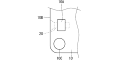
- Fig. 3 is a plan view showing a part of the configuration of a heat sink 10 of the semiconductor device 102.
- the semiconductor device 102 in the second embodiment is manufactured using the second manufacturing process described in the first embodiment, and shows a state in which the screw hole 20 (first screw hole) and the position determination portion 10A are provided in advance in the heat sink 10.
- 10C is a screw hole for fixing the heat sink 10 to the object on which the semiconductor device 102 is to be installed.
- the case 70 is fastened to the heat sink 10 by tapping screws 21 screwed into the screw holes 20.
- the tips of the tapping screws 21 are contained within the heat sink 10 and are not exposed to the internal space of the case 70, which is filled with the sealing material 80.
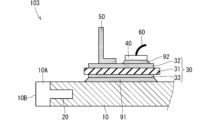
- Fig. 4 is a cross-sectional view showing the configuration of a semiconductor device 103 in the third embodiment.
- Fig. 5 is a cross-sectional view showing a part of the configuration of the semiconductor device 103.
- Fig. 6 is a plan view showing a part of the configuration of a heat sink 10 of the semiconductor device 103.
- the semiconductor device 103 in the third embodiment differs from the semiconductor device 101 in the configuration of a position determining portion 10A of the heat sink 10 and a case 70 that fits into the position determining portion 10A.
- the positioning portion 10A includes a notch provided on the outer edge of the heat sink 10.
- the notch is provided on the side surface 10B of the heat sink 10 so as to overlap with the opening of the screw hole 20.
- the case 70 includes a protrusion 71 that fits into the cutout.
- the case 70 is fastened to the heat sink 10 by a tapping screw 21 screwed into the screw hole 20.
- the tip of the tapping screw 21 penetrates the protrusion 71 of the case 70 from the outside of the case 70.
- the tip of the tapping screw 21 is contained inside the heat sink 10 and is not exposed to the internal space of the case 70 filled with the sealing material 80.
- the first manufacturing process or the second manufacturing process described in the first embodiment can be applied.
- the case 70 fits into the positioning portion 10A of the heat sink 10, it becomes easier to position the case 70 when joining the heat sink 10 and the case 70 in the manufacturing process. As a result, a jig for fixing the positions of the heat sink 10 and the case 70 is no longer necessary, improving workability.
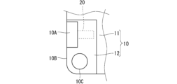
- ⁇ Fourth embodiment> 7 and 8 are plan views showing a part of the configuration of heat sink 10 of the semiconductor device according to the fourth embodiment. As shown in Figs. 7 and 8, the semiconductor device according to the fourth embodiment has a different configuration of heat sink 10 from semiconductor device 101 according to the first embodiment and semiconductor device 103 according to the third embodiment.
- the heat sink 10 in the fourth embodiment includes a first region 11 and a second region 12.
- the first region 11 is made of AlSiC.
- the second region 12 is made of Al.
- the semiconductor element 40 is arranged so as to overlap the first region 11 in a plan view.
- the screw hole 20 and the position determination portion 10A are provided in the second region 12.
- the case 70 is fastened to the heat sink 10 by tapping screws 21 screwed into the screw holes 20.
- the material of the tapping screws 21 is Al, which is harder than the material of the second region 12 of the heat sink 10.
- the first manufacturing process or the second manufacturing process described in the first embodiment can be applied. Since the material of the second region 12 of the heat sink 10 is Al, which is softer than the material of a typical tapping screw 21, the first manufacturing process can be easily applied.
- the semiconductor element 40 is located above the first region 11 made of AlSiC, improving heat dissipation.
- the screw holes 20 are located in the second region 12 made of Al, which is softer than AlSiC, making it easy to form and fasten the screw holes 20 with the tapping screws 21. In other words, there is no need to prepare a heat sink 10 with the screw holes 20 already formed before fastening with the tapping screws 21. This reduces the number of processing steps required to manufacture the heat sink 10.
- ⁇ Fifth embodiment> 9 is a cross-sectional view showing the configuration of a semiconductor device 105 according to the fifth embodiment.
- the semiconductor device 105 according to the fifth embodiment differs from the semiconductor device 101 according to the first embodiment in the configurations of the heat sink 10 and the case 70.
- the case 70 is arranged so that the inner surface 70A of the frame of the case 70 is in contact with the side surface 10B that forms the outer edge of the heat sink 10.
- the case 70 may be in contact with the entire surface of at least one of the four side surfaces 10B of the heat sink 10.
- the case 70 is fastened to the heat sink 10 by a tapping screw 21 that is screwed into a screw hole 20 from the outer surface 70B of the frame of the case 70.
- the tip of the tapping screw 21 penetrates the case 70 from the outer surface 70B of the frame of the case 70.
- the tip of the tapping screw 21 is located inside the screw hole 20 of the heat sink 10. The tip of the tapping screw 21 is not exposed to the internal space of the case 70 that is filled with the sealing material 80.
- the first manufacturing process or the second manufacturing process described in the first embodiment can be applied.
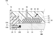
- ⁇ Sixth embodiment> 10 is a cross-sectional view showing the configuration of a semiconductor device 106 according to the sixth embodiment. This is an embodiment particularly suitable for the application of the second manufacturing process described in the first embodiment.
- the screw hole 20 includes a hollow portion at its innermost portion.
- the hollow portion is formed, for example, by the tip of the tapping screw 21 and the innermost margin of the screw hole 20 that was previously formed in the heat sink 10.
- the heat sink 10 contains scraps 20B inside the screw holes 20, which are made of the same material as the heat sink 10 or the case 70.
- the scraps 20B are trapped in the hollow portion at the innermost part of the screw holes 20.
- the scraps 20B are generated during the manufacturing process of the semiconductor device 106.
- the second manufacturing process described in the first embodiment is applied to the manufacturing process of the semiconductor device 106.
- the screw hole 20 has an opening in the side surface 10B of the heat sink 10.
- the tapping screw 21 is screwed into the screw hole 20.
- the material of the heat sink 10 and the protrusion 71 of the case 70 is scraped off, generating scraps made of the same material as the case 70 and scraps made of the same material as the heat sink 10.
- the tip of the tapping screw 21 does not reach the innermost part of the screw hole 20. Therefore, the debris 20B generated during the process of forming the screw hole 20 is trapped in the hollow part at the tip of the screw hole 20.
- the tip of the tapping screw 21 is contained within the heat sink 10 and is not exposed to the internal space of the case 70 filled with the sealing material 80. Also, because the screw hole 20 is not a through hole, the debris 20B generated when the screw hole 20 is formed does not scatter to the outside. The potential of the tapping screw 21 and the heat sink 10 is GND, so partial discharge caused by the debris 20B is prevented.
- each embodiment can be freely combined, modified, or omitted as appropriate.
Landscapes
- Cooling Or The Like Of Semiconductors Or Solid State Devices (AREA)
- Cooling Or The Like Of Electrical Apparatus (AREA)
Priority Applications (4)
| Application Number | Priority Date | Filing Date | Title |
|---|---|---|---|
| CN202380090853.6A CN120548610A (zh) | 2023-01-30 | 2023-01-30 | 半导体装置 |
| PCT/JP2023/002837 WO2024161451A1 (ja) | 2023-01-30 | 2023-01-30 | 半導体装置 |
| DE112023005705.2T DE112023005705T5 (de) | 2023-01-30 | 2023-01-30 | Halbleitervorrichtung |
| JP2024574065A JP7834209B2 (ja) | 2023-01-30 | 2023-01-30 | 半導体装置 |
Applications Claiming Priority (1)
| Application Number | Priority Date | Filing Date | Title |
|---|---|---|---|
| PCT/JP2023/002837 WO2024161451A1 (ja) | 2023-01-30 | 2023-01-30 | 半導体装置 |
Publications (1)
| Publication Number | Publication Date |
|---|---|
| WO2024161451A1 true WO2024161451A1 (ja) | 2024-08-08 |
Family
ID=92146273
Family Applications (1)
| Application Number | Title | Priority Date | Filing Date |
|---|---|---|---|
| PCT/JP2023/002837 Ceased WO2024161451A1 (ja) | 2023-01-30 | 2023-01-30 | 半導体装置 |
Country Status (4)
| Country | Link |
|---|---|
| JP (1) | JP7834209B2 (https=) |
| CN (1) | CN120548610A (https=) |
| DE (1) | DE112023005705T5 (https=) |
| WO (1) | WO2024161451A1 (https=) |
Citations (4)
| Publication number | Priority date | Publication date | Assignee | Title |
|---|---|---|---|---|
| JPS54101973U (https=) * | 1977-12-27 | 1979-07-18 | ||
| JP2011503852A (ja) * | 2007-11-13 | 2011-01-27 | シーメンス アクチエンゲゼルシヤフト | パワー半導体素子モジュール |
| WO2016006065A1 (ja) * | 2014-07-09 | 2016-01-14 | 三菱電機株式会社 | 半導体装置 |
| JP2017199756A (ja) * | 2016-04-26 | 2017-11-02 | 日本電気株式会社 | 冷却部材、冷却装置、電子機器および冷却部材の形成方法 |
Family Cites Families (3)
| Publication number | Priority date | Publication date | Assignee | Title |
|---|---|---|---|---|
| JPH11262273A (ja) * | 1998-03-11 | 1999-09-24 | Denso Corp | パワーモジュール装置及びその製造方法 |
| JP2001307542A (ja) | 2000-04-26 | 2001-11-02 | Toshiba Lighting & Technology Corp | 電子式放電ランプ点灯装置 |
| JP5855899B2 (ja) | 2011-10-27 | 2016-02-09 | 日立オートモティブシステムズ株式会社 | Dc−dcコンバータ及び電力変換装置 |
-
2023
- 2023-01-30 JP JP2024574065A patent/JP7834209B2/ja active Active
- 2023-01-30 WO PCT/JP2023/002837 patent/WO2024161451A1/ja not_active Ceased
- 2023-01-30 DE DE112023005705.2T patent/DE112023005705T5/de active Pending
- 2023-01-30 CN CN202380090853.6A patent/CN120548610A/zh active Pending
Patent Citations (4)
| Publication number | Priority date | Publication date | Assignee | Title |
|---|---|---|---|---|
| JPS54101973U (https=) * | 1977-12-27 | 1979-07-18 | ||
| JP2011503852A (ja) * | 2007-11-13 | 2011-01-27 | シーメンス アクチエンゲゼルシヤフト | パワー半導体素子モジュール |
| WO2016006065A1 (ja) * | 2014-07-09 | 2016-01-14 | 三菱電機株式会社 | 半導体装置 |
| JP2017199756A (ja) * | 2016-04-26 | 2017-11-02 | 日本電気株式会社 | 冷却部材、冷却装置、電子機器および冷却部材の形成方法 |
Also Published As
| Publication number | Publication date |
|---|---|
| CN120548610A (zh) | 2025-08-26 |
| JP7834209B2 (ja) | 2026-03-23 |
| JPWO2024161451A1 (https=) | 2024-08-08 |
| DE112023005705T5 (de) | 2025-11-06 |
Similar Documents
| Publication | Publication Date | Title |
|---|---|---|
| JP3168901B2 (ja) | パワー半導体モジュール | |
| JP6288254B2 (ja) | 半導体モジュールおよびその製造方法 | |
| CN111081643B (zh) | 半导体装置及半导体装置的制造方法 | |
| CN104517909A (zh) | 带有印制电路板的半导体模块及其制造方法 | |
| WO2017094189A1 (ja) | 半導体モジュール | |
| JP2025094258A (ja) | 半導体装置、および半導体装置の製造方法 | |
| US20250210424A1 (en) | Semiconductor device and method for manufacturing semiconductor device | |
| JP7834209B2 (ja) | 半導体装置 | |
| JP7778271B2 (ja) | 半導体装置及びその製造方法 | |
| JP2025074405A (ja) | 半導体モジュールおよび半導体モジュールの製造方法 | |
| JPH09237869A (ja) | 樹脂封止型パワーモジュール装置及びその製造方法 | |
| JP6891075B2 (ja) | パワー半導体モジュール | |
| WO2021261056A1 (ja) | パワーモジュール | |
| CN110416178A (zh) | 一种集成电路封装结构及其封装方法 | |
| JP7803460B2 (ja) | 放熱ベース、半導体モジュール、及びエネルギー変換装置 | |
| US12087651B2 (en) | Semiconductor device and method of manufacturing the same | |
| JP7838443B2 (ja) | 半導体装置 | |
| US12400973B2 (en) | Semiconductor device | |
| JP7822489B2 (ja) | 半導体装置 | |
| JP7482833B2 (ja) | 半導体装置および半導体装置の製造方法 | |
| US20240266265A1 (en) | Semiconductor device | |
| US11721615B2 (en) | Coupled semiconductor package | |
| US20240312880A1 (en) | Semiconductor device, method of manufacturing the same, and power conversion device | |
| WO2025120688A1 (ja) | 半導体装置 | |
| WO2025192056A1 (ja) | 半導体装置 |
Legal Events
| Date | Code | Title | Description |
|---|---|---|---|
| 121 | Ep: the epo has been informed by wipo that ep was designated in this application |
Ref document number: 23919596 Country of ref document: EP Kind code of ref document: A1 |
|
| WWE | Wipo information: entry into national phase |
Ref document number: 2024574065 Country of ref document: JP |
|
| WWE | Wipo information: entry into national phase |
Ref document number: 202380090853.6 Country of ref document: CN |
|
| WWP | Wipo information: published in national office |
Ref document number: 202380090853.6 Country of ref document: CN |
|
| WWE | Wipo information: entry into national phase |
Ref document number: 112023005705 Country of ref document: DE |
|
| 122 | Ep: pct application non-entry in european phase |
Ref document number: 23919596 Country of ref document: EP Kind code of ref document: A1 |