WO2024157825A1 - 基板搬送方法、基板処理装置及びプログラム - Google Patents
基板搬送方法、基板処理装置及びプログラム Download PDFInfo
- Publication number
- WO2024157825A1 WO2024157825A1 PCT/JP2024/000841 JP2024000841W WO2024157825A1 WO 2024157825 A1 WO2024157825 A1 WO 2024157825A1 JP 2024000841 W JP2024000841 W JP 2024000841W WO 2024157825 A1 WO2024157825 A1 WO 2024157825A1
- Authority
- WO
- WIPO (PCT)
- Prior art keywords
- module
- substrate
- transport mechanism
- lot
- substrates
- Prior art date
- Legal status (The legal status is an assumption and is not a legal conclusion. Google has not performed a legal analysis and makes no representation as to the accuracy of the status listed.)
- Ceased
Links
Images




Classifications
-
- G—PHYSICS
- G03—PHOTOGRAPHY; CINEMATOGRAPHY; ANALOGOUS TECHNIQUES USING WAVES OTHER THAN OPTICAL WAVES; ELECTROGRAPHY; HOLOGRAPHY
- G03F—PHOTOMECHANICAL PRODUCTION OF TEXTURED OR PATTERNED SURFACES, e.g. FOR PRINTING, FOR PROCESSING OF SEMICONDUCTOR DEVICES; MATERIALS THEREFOR; ORIGINALS THEREFOR; APPARATUS SPECIALLY ADAPTED THEREFOR
- G03F7/00—Photomechanical, e.g. photolithographic, production of textured or patterned surfaces, e.g. printing surfaces; Materials therefor, e.g. comprising photoresists; Apparatus specially adapted therefor
- G03F7/70—Microphotolithographic exposure; Apparatus therefor
- G03F7/70691—Handling of masks or workpieces
- G03F7/70733—Handling masks and workpieces, e.g. exchange of workpiece or mask, transport of workpiece or mask
- G03F7/7075—Handling workpieces outside exposure position, e.g. SMIF box
-
- G—PHYSICS
- G03—PHOTOGRAPHY; CINEMATOGRAPHY; ANALOGOUS TECHNIQUES USING WAVES OTHER THAN OPTICAL WAVES; ELECTROGRAPHY; HOLOGRAPHY
- G03F—PHOTOMECHANICAL PRODUCTION OF TEXTURED OR PATTERNED SURFACES, e.g. FOR PRINTING, FOR PROCESSING OF SEMICONDUCTOR DEVICES; MATERIALS THEREFOR; ORIGINALS THEREFOR; APPARATUS SPECIALLY ADAPTED THEREFOR
- G03F7/00—Photomechanical, e.g. photolithographic, production of textured or patterned surfaces, e.g. printing surfaces; Materials therefor, e.g. comprising photoresists; Apparatus specially adapted therefor
- G03F7/70—Microphotolithographic exposure; Apparatus therefor
- G03F7/708—Construction of apparatus, e.g. environment aspects, hygiene aspects or materials
- G03F7/70991—Connection with other apparatus, e.g. multiple exposure stations, particular arrangement of exposure apparatus and pre-exposure and/or post-exposure apparatus; Shared apparatus, e.g. having shared radiation source, shared mask or workpiece stage, shared base-plate; Utilities, e.g. cable, pipe or wireless arrangements for data, power, fluids or vacuum
-
- H—ELECTRICITY
- H10—SEMICONDUCTOR DEVICES; ELECTRIC SOLID-STATE DEVICES NOT OTHERWISE PROVIDED FOR
- H10P—GENERIC PROCESSES OR APPARATUS FOR THE MANUFACTURE OR TREATMENT OF DEVICES COVERED BY CLASS H10
- H10P72/00—Handling or holding of wafers, substrates or devices during manufacture or treatment thereof
- H10P72/04—Apparatus for manufacture or treatment
- H10P72/0451—Apparatus for manufacturing or treating in a plurality of work-stations
- H10P72/0468—Apparatus for manufacturing or treating in a plurality of work-stations comprising a chamber adapted to a particular process
- H10P72/0474—Apparatus for manufacturing or treating in a plurality of work-stations comprising a chamber adapted to a particular process comprising at least one lithography chamber
-
- H—ELECTRICITY
- H10—SEMICONDUCTOR DEVICES; ELECTRIC SOLID-STATE DEVICES NOT OTHERWISE PROVIDED FOR
- H10P—GENERIC PROCESSES OR APPARATUS FOR THE MANUFACTURE OR TREATMENT OF DEVICES COVERED BY CLASS H10
- H10P72/00—Handling or holding of wafers, substrates or devices during manufacture or treatment thereof
- H10P72/30—Handling or holding of wafers, substrates or devices during manufacture or treatment thereof for conveying, e.g. between different workstations
-
- H—ELECTRICITY
- H10—SEMICONDUCTOR DEVICES; ELECTRIC SOLID-STATE DEVICES NOT OTHERWISE PROVIDED FOR
- H10P—GENERIC PROCESSES OR APPARATUS FOR THE MANUFACTURE OR TREATMENT OF DEVICES COVERED BY CLASS H10
- H10P72/00—Handling or holding of wafers, substrates or devices during manufacture or treatment thereof
- H10P72/30—Handling or holding of wafers, substrates or devices during manufacture or treatment thereof for conveying, e.g. between different workstations
- H10P72/33—Handling or holding of wafers, substrates or devices during manufacture or treatment thereof for conveying, e.g. between different workstations into and out of processing chamber
- H10P72/3302—Mechanical parts of transfer devices
-
- H—ELECTRICITY
- H10—SEMICONDUCTOR DEVICES; ELECTRIC SOLID-STATE DEVICES NOT OTHERWISE PROVIDED FOR
- H10P—GENERIC PROCESSES OR APPARATUS FOR THE MANUFACTURE OR TREATMENT OF DEVICES COVERED BY CLASS H10
- H10P72/00—Handling or holding of wafers, substrates or devices during manufacture or treatment thereof
- H10P72/30—Handling or holding of wafers, substrates or devices during manufacture or treatment thereof for conveying, e.g. between different workstations
- H10P72/34—Handling or holding of wafers, substrates or devices during manufacture or treatment thereof for conveying, e.g. between different workstations the wafers being stored in a carrier, involving loading and unloading
- H10P72/3402—Mechanical parts of transfer devices
-
- H—ELECTRICITY
- H10—SEMICONDUCTOR DEVICES; ELECTRIC SOLID-STATE DEVICES NOT OTHERWISE PROVIDED FOR
- H10P—GENERIC PROCESSES OR APPARATUS FOR THE MANUFACTURE OR TREATMENT OF DEVICES COVERED BY CLASS H10
- H10P72/00—Handling or holding of wafers, substrates or devices during manufacture or treatment thereof
- H10P72/30—Handling or holding of wafers, substrates or devices during manufacture or treatment thereof for conveying, e.g. between different workstations
- H10P72/34—Handling or holding of wafers, substrates or devices during manufacture or treatment thereof for conveying, e.g. between different workstations the wafers being stored in a carrier, involving loading and unloading
- H10P72/3404—Storage means
-
- H—ELECTRICITY
- H10—SEMICONDUCTOR DEVICES; ELECTRIC SOLID-STATE DEVICES NOT OTHERWISE PROVIDED FOR
- H10P—GENERIC PROCESSES OR APPARATUS FOR THE MANUFACTURE OR TREATMENT OF DEVICES COVERED BY CLASS H10
- H10P76/00—Manufacture or treatment of masks on semiconductor bodies, e.g. by lithography or photolithography
Definitions
- This disclosure relates to a substrate transport method, a substrate processing apparatus, and a program.
- wafers When manufacturing semiconductor devices, photolithography is performed on semiconductor wafers (hereinafter referred to as wafers). Specifically, after a resist film is exposed to light in a predetermined pattern in an exposure machine, the wafer is transported between modules in a substrate processing apparatus so that it is heated and developed, called PEB (Post Exposure Bake). Patent Document 1 shows that the wafer is transported so that the time until PEB is performed is constant after exposure.
- PEB Post Exposure Bake
- This disclosure provides technology that can reduce variation in the transport state between substrates after exposure by an exposure machine and reduce variation in the pattern formed on the substrate by development.
- the substrate transport method of the present disclosure includes a transport mechanism group that transports a substrate removed from a carrier to the carrier via a module group and an exposure machine; the module group includes a first subsequent stage module, a second subsequent stage module, a heating module, and a developing module, each of which is located downstream of the exposure machine and on which the substrate is placed; a first subsequent stage transport mechanism that transports the substrate from the carrier to the exposure machine, a first subsequent stage transport mechanism that transports the substrate from the exposure machine to the first subsequent stage module, a second subsequent stage transport mechanism that transports the substrate through the first subsequent stage module, the heating module, the developing module, and the second subsequent stage module in that order, and a third subsequent stage transport mechanism that transports the substrate from the second subsequent stage module to the carrier,
- the substrate processing apparatus includes a storage module for storing the substrate in an area forming an atmosphere different from the surroundings, a storing step of transporting the plurality of substrates belonging to the same lot, which have been removed from the exposure machine and have not yet been received by the second post
- This disclosure can reduce variation in the transport state between substrates after exposure by an exposure machine, and reduce variation in the pattern formed on the substrate by development.
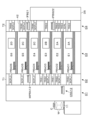
- FIG. 2 is a plan view of a coating and developing apparatus according to an embodiment of the present disclosure.
- FIG. 2 is a vertical sectional side view of the coating and developing apparatus.
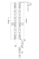
- 3 is a block diagram showing a transport path in the coating and developing apparatus.
- FIG. FIG. 4 is a block diagram showing the transport path on the rear side of the exposure machine.
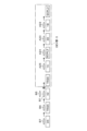
- FIG. 2 is a block diagram showing an outline of transport control.
- FIG. 2 is a block diagram showing an outline of transport control.
- FIG. 2 is a block diagram showing an outline of transport control.
- FIG. 13 is a block diagram showing an example of transportation.
- FIG. 13 is a block diagram showing an example of transportation.
- FIG. 13 is a block diagram showing an example of transportation.
- FIG. 13 is a block diagram showing another example of transportation.
- This coating and developing apparatus 1 coats a wafer W, which is a substrate, with resist to form a resist film, and transports the wafer W to an exposure machine D5. After the exposure machine D5 exposes the resist film to light according to a predetermined pattern, the coating and developing apparatus 1 supplies a developer to the wafer W to perform a development process and form a resist pattern.
- One of the resists CAR (Chemical Amplification Resist: CAR) and MOR (Metal Oxide Resist: MOR), is supplied to the wafer W to form the resist film.
- the wafer W supplied with CAR is developed with a positive developer, and the wafer W supplied with MOR is developed with a negative developer.
- one of a plurality of different types of resists is selected and supplied to the wafer W, and further, one of a plurality of different types of developers is selected and supplied depending on the type of resist selected.
- the wafer W on which the MOR resist film is formed and the wafer W on which the CAR resist film is formed are transported by different routes in the coating and developing device 1. Regardless of whether the resist film formed is CAR or MOR, the wafer W is subjected to PEB after exposure and before development.
- a buffer module 42 capable of waiting multiple wafers W under an N2 (nitrogen) gas atmosphere is provided on the transport path of the wafers W on which the MOR resist film is formed.
- the wafers W are transported so that the PPD times are uniform within the same lot, and by waiting the wafers W in this buffer module 42, the deterioration of the resist due to the atmosphere is suppressed to prevent deviations in the PED times, and thus CD variations are prevented.
- MOR is a metal-containing resist. "Containing a metal” here means that the metal is included as a constituent component, not that the metal is included as an impurity.
- the coating and developing apparatus 1 is configured by connecting a carrier block D1, an intermediate block D2, a processing block D3, and an interface block D4 in a row from left to right.
- An exposure machine D5 is connected to the right side of the interface block D4 (the side opposite to the side where the carrier block D1 is located).
- the carrier block D1 is equipped with multiple stages 11, and each of these stages 11 can accommodate a carrier C, which is a transport container called a FOUP (Front Opening Unify Pod) capable of storing wafers W. A maximum of 25 wafers W can be stored in the carrier C.
- the carrier block D1 also includes a transport mechanism 12, which transfers wafers W to and from the carrier C on the stage 11.
- the intermediate block D2 is provided with a tower T1 in which many modules are stacked. Each module of the tower T1 is accessible by the above-mentioned transfer mechanism 12 and the transfer mechanism 13 arranged at the rear side of the tower T1, and the above-mentioned transfer mechanism 12.
- the transfer mechanisms 12 and 13 work together to enable the transfer of wafers W between each floor of the processing block D3 described below and the carrier C.
- Processing block D3 is composed of levels E1 to E6, which are stacked in order from the bottom up and perform liquid processing and heating processing on wafers W.
- Levels E1 to E3 form resist films, levels E1 and E2 apply CAR, and level E3 applies MOR.
- Levels E4 to E6 form resist patterns through PEB and development.
- a transport path 14 for wafers W extending from left to right is formed in the center between the front and rear of level E6.
- multiple development modules 2D for MOR development are arranged side by side.
- heating modules for heating wafers W are stacked, and many stacks of these heating modules are arranged side by side.
- These heating modules include those that perform PEB and those that perform post-development heating (post-bake).
- two types of heating modules, 1A and 1B are installed, with heating module 1A performing PEB and heating module 1B performing post-bake.
- Heating modules 1A and 1B are equipped with hot plates on which wafers W are placed and heated, and the temperature of these hot plates can be changed freely.
- the above-mentioned transfer path 14 is provided with a transfer mechanism 36 that transfers wafers W on level E6.
- the transfer mechanism 36 has a base that moves on the transfer path 14, and two substrate holding parts that move forward and backward on the base. One of the substrate holding parts moves forward and backward to receive the wafer W from the module, and then the other substrate holding part enters the module and sends the wafer W, allowing the wafer W to be swapped and handed over at the module.
- This swapping of the module is sometimes referred to as swapping transfer.
- a module is a place where the wafer W is placed other than the transfer mechanism, and a module that processes the wafer W is sometimes referred to as a processing module.
- the levels E4 and E5 have the same configuration as level E6, except that they are equipped with a developing module 2C for CAR development instead of a developing module 2D for MOR development.
- Levels E1 to E2 are equipped with a coating module 2A that supplies CAR to the wafer W instead of the developing module 2D
- level E3 is equipped with a coating module 2A that supplies MOR to the wafer W instead of the developing module 2D.
- the heating modules on levels E1 to E3 heat the wafer W after the resist film has been formed.
- levels E1 to E3 have the same configuration as level E6.
- the transport mechanisms on levels E1 to E5, which correspond to transport mechanism 36, are designated 31 to 35.
- the interface block D4 is equipped with the tower T2 and the transport mechanisms 21 and 22.
- the tower T2 has many stacked modules, similar to the tower T1.
- the transport mechanism 21 is used for transport between the modules of the tower T2 and is provided on the front side of the tower T2.
- the transport mechanism 22 is used for transport between the modules of the tower T2 and the exposure machine D5 and is provided on the right side of the tower T2.
- the towers T1 and T2 are described below.
- the towers T1 and T2 are provided with a transfer module TRS and a temperature adjustment module SCPL, which are used for loading and unloading the levels E1 to E6, and for transferring the wafer W between blocks and between the blocks and the exposure machine D5.
- the SCPL is a module that adjusts the temperature of the wafer W, and in addition to the above-mentioned loading and unloading and transfer between blocks, it also includes a module that adjusts the temperature of the wafer W being transported between levels and a module that adjusts the temperature of the wafer W immediately before it is transported to the exposure machine.
- the SCPL that adjusts the temperature of the wafer W immediately before it is transported to the exposure machine D5 is referred to as ICPL.
- TRSs and SCPLs for each of the above purposes are provided.
- the TRSs and SCPLs may be appropriately numbered to distinguish between modules located in different locations.
- the number of wafers W that can be placed on the TRS and SCPL is not limited to one, and two wafers W can be placed on the TRS5 in the figure.
- a buffer module 42 which is a storage module, is provided on the front side of the transfer mechanism 21.
- the buffer module 42 has a housing that can load and unload wafers W from the side, and can store wafers W lined up vertically inside the housing.
- the buffer module 42 can store 36 or more wafers W, the reason for which will be described later.
- a supply port for supplying N2 gas is opened in the above-mentioned housing, and the inside of the housing is made into an N2 gas atmosphere. Therefore, the atmosphere in the area in which the wafer W is stored in the housing is different from the atmosphere outside the housing. It is considered that the change in the properties of the MOR after exposure that causes the above-mentioned CD variation of the pattern is largely due to the effect of moisture contained in the atmosphere. Therefore, the gas to be supplied into the housing is a gas that makes the atmosphere different between the inside and outside of the housing, and more specifically, a gas that makes the relative humidity inside the housing lower than that outside the housing is preferably used.
- the gas used is not limited to N2 gas, and a configuration in which an inert gas other than N2 gas, such as argon gas, or a gas such as dry air having a lower water content than the atmosphere around the housing is supplied into the housing may be used.
- an inert gas other than N2 gas such as argon gas, or a gas such as dry air having a lower water content than the atmosphere around the housing is supplied into the housing may be used.
- the exposure machine D5 outputs a signal (in-ready signal) when the wafer W can be loaded, and outputs a signal (out-ready signal) when the wafer W can be unloaded.
- the control unit 4 described below receives these signals and controls the operation of the transport mechanism 22, and the wafer W is transferred between the interface block D4 and the exposure machine D5.
- the exposure machine cycle time is the interval from when a wafer W is loaded into the exposure machine D5 to when the exposure of the wafer W is completed and the out-ready signal is output.
- the exposure machine cycle time is constant or approximately constant, and if the wafers W are transported at a constant cycle, the out-ready signal is output at a constant or approximately constant cycle.
- a maximum of nine wafers W can be loaded into the exposure machine D5.
- a process job (PJ) is set for the wafer W in the carrier C by the control unit 4, which will be described later.
- the PJ is information that specifies the processing recipe for the wafer W (including a transfer recipe specifying which type of module the wafer W should be transferred to for processing, or which module of the same type the wafer W should be transferred to) and the wafer W to be transferred. Therefore, the transfer path of the wafer W in the coating and developing apparatus 1 is specified by the PJ. Wafers W in the same PJ undergo the same processing, so wafers W in the same PJ are wafers W from the same lot.
- the processing recipe specified by the PJ includes information for calculating the required residence time of the wafer W in each processing module (MUT: Module Using Time). Specifically, this MUT is calculated based on the processing time of the wafer W. Even for the same processing module, the processing time differs depending on the processing recipe specified, and the MUT will also differ.
- MUT Module Using Time
- each transport mechanism is controlled by the control unit 4 described below so that the wafers W from one PJ are successively transported into the apparatus, and then the wafers W from the other PJ are successively transported into the apparatus.
- the wafers W from the preceding PJ are transported into the apparatus all at once
- the wafers W from the succeeding PJ are transported into the apparatus all at once.
- each wafer W is transported along the transport path specified by each PJ, and is processed in each processing module along the transport path according to the processing recipe specified by each PJ.
- Wafers W from the same PJ are transported to the subsequent module in the order in which they were transported into the apparatus.
- the wafers W are transported to the exposure machine D5 in order in groups by PJ.
- the transport mechanisms 12 and 13 may be referred to as CRA12 and MPRA13, the transport mechanisms 31 to 36 as PRA31 to 36, and the transport mechanisms 21 and 22 as IFB21 and IFBS22.
- each section where transport is performed by a different transport mechanism is referred to as a "layer.”
- the layers corresponding to PRAs 31, 32, and 33 are referred to as COT layer-1, COT layer-2, and COT layer-3, respectively, and the layers corresponding to PRAs 34, 35, and 36 are referred to as DEV layer-1, DEV layer-2, and DEV layer-3, respectively.
- PRAs 31 to 36 move repeatedly through the modules in the layer in order, and perform the above-mentioned wafer W replacement transport to each module except for the entrance and exit modules of the layer. Therefore, the transport mechanism moves around the transport path 14. By the operation of this transport mechanism, the wafers W are transported one by one from the upstream module to the downstream module. Note that when switching PJs, there may be gaps in the intervals between the transport of wafers W to the modules, and therefore replacement transport may not be possible.
- [Description of conveying route] 3 shows an outline of the transport path in the coating and developing apparatus 1, with solid arrows and dotted arrows indicating the transport path of the wafer W in the MOR PJ (PJ where the MOR resist film is formed and developed) and the transport path of the wafer W in the CAR PJ (PJ where the CAR resist film is formed and developed), respectively.
- the wafer W in the MOR PJ is returned to the carrier C via the COT layer-3, exposure machine D5, and DEV layer-3 in this order.
- the wafer W in the CAR PJ is sorted from the carrier C to the COT layer-1 and COT layer-2, and is transported to the exposure machine D5 via these layers, and then sorted to the DEV layer-1 and DEV layer-2, and is returned to the carrier C via these layers.
- FIG. 4 shows the transport path of the exposure machines D5 to DEV layers.
- FIG. 4 shows the transport path of the exposure machines D5 to DEV layers.
- the transport path of the wafer W in the PJ of the MOR and the transport path of the wafer W in the PJ of the CAR are indicated by solid arrows and dotted arrows, respectively.
- the transport mechanism used for the transport indicated by the arrow is shown near the arrow.
- the wafer W is removed from the carrier C by CRA12 and transported to the transfer module TRS1 of tower T1, and then transported by MPRA13 to the transfer module TRS2 at the height of floor E3 in tower T1.
- the wafer W is then received by PRA33 and transported in the following order: temperature adjustment module SCPL1 ⁇ coating module 2B ⁇ heating module.
- the wafer W thus transported and with the MOR resist film formed thereon is transported to the transfer module TRS3 of tower T2, and then transported in the following order: IFB21 ⁇ TRS4 of tower T2 ⁇ IFB21 ⁇ ICPL ⁇ IFBS22 ⁇ exposure machine D5, where the resist film is exposed according to a specified pattern.
- the wafer W is transported in the order IFBS22 ⁇ TRS5 of tower T2, then transported by IFB21 to buffer module 42, and then transported by IFB21 to TRS6 (the entrance to DEV layer-3) at the height of floor E6 of tower T2.
- the wafer W is received by PRA36 and transported in the order heating module 1A ⁇ SCPL2 of tower T2 ⁇ developing module 2D, where a resist pattern is formed on the wafer W.
- the wafer W is then transported in the order heating module 1B ⁇ SCPL3 of tower T1 (the exit of DEV layer-3), and then transported in the order MPRA13 ⁇ transfer module TRS7 of tower T1 ⁇ CRA12 ⁇ carrier C.
- Differences between the transport path of wafer W in CAR's PJ and the transport path of wafer W in MOR's PJ include that it is transported to COT layers-1, 2 and DEV layers-1, 2 by PRAs 31, 32, 34, 35; within COT layers-1, 2, the wafer W is transported to coating module 2A instead of coating module 2B; in DEV layers-1, 2, it is transported to development module 2C instead of development module 2D; the TRS and CPL to which the wafer W is handed over are located at the heights of COT layers-1, 2 and DEV layers-1, 2 instead of the heights of COT layer-3 and DEV layer-3 in towers T1 and T2; and it is transported by IFBS 22 from exposure machine D5 to the module at the entrance of DEV layers 1 and 2 in tower T2 without passing through TRS 5 and buffer module 42.
- the entry and exit modules of DEV layers-1 and -2 are denoted as TRS6' and SCPL3', respectively.
- TRS6 and TRS6' correspond to the first subsequent stage module
- SCPL3 and SCPL3' correspond to the second subsequent stage module
- TRS5 corresponds to the third subsequent stage module.
- CRA12, MPRA13, and PRAs 34-36 constitute a front-stage transport mechanism
- IFB21 and IFBS22 correspond to the first subsequent stage transport mechanism
- PRAs 34-36 correspond to the second subsequent stage transport mechanism
- MPRA13 and CRA12 constitute a third subsequent stage transport mechanism.
- levels E4-E6 if the first subsequent stage module, second subsequent stage module, PEB heating module, development module, and PRA that transports between these modules are considered as a group, there will be three such groups.
- the coating and developing apparatus 1 includes a control unit 4 which is a computer.
- the control unit 4 includes a program 41.
- the program 41 is structured to include steps for transporting the wafer W and processing the wafer W in each module, which will be described later, and outputs control signals to each module and each transport mechanism for the wafer W. Each module and transport mechanism operates in response to the control signals.
- the program 41 is stored in a storage medium, such as a compact disc, a hard disk, or a DVD, and is installed in the control unit 4. Furthermore, the program 41 is configured to perform various calculations, comparisons, and judgments required to perform each transport control, which will be described later, thereby enabling the execution of each transport control.
- the PRA 36 of the DEV-layer-3 for MOR is transported by rotating around the transport path 14 and accessing each processing module in turn to replace the wafer W.
- the number of MUTs/multi-modules in use is calculated for each of the processing modules other than the entrance and exit of the DEV-layer 3, namely, the heating module 1A, SCPL2, developing module 2D, and heating module 1B, and the time for the PRA 36 to make one revolution (circumnavigation movement time) is determined from each calculated value.
- the orbital movement time is determined as the larger of the maximum value among the calculated values and the number of transport steps by PRA36 from the entrance to the exit of the layer multiplied by a predetermined time, and PRA36 orbits the transport path 14 during this orbital movement time.
- the number of transport steps is counted as five, since the wafer W is transported in the order TRS6 ⁇ heating module 1A ⁇ temperature adjustment module SCPL2 ⁇ developing module 2D ⁇ heating module 1B ⁇ SCPL3.
- the orbital movement time of PRA36 in DEV layer-3 corresponds to the PJ transported to this DEV layer-3.
- the orbital movement time of the PRA is determined in the same manner for the COT layer and DEV layers-1 and -2, but detailed description is omitted.
- the wafer W of the PJ that passed through the exposure machine D5 first is the wafer W of the leading PJ, and the wafer W of the PJ that passed through the exposure machine D5 after the wafer W is the wafer W of the trailing PJ.
- the wafer W of the leading PJ is a wafer W belonging to the leading lot
- the wafer W of the trailing PJ is a wafer W belonging to the trailing lot.
- the wafer W of the trailing PJ is made to wait in the buffer module 42 and is not transported to DEV layer-3.
- the wafer W of the leading PJ is being transported to DEV layer-3 refers to the period from when the first wafer W of the leading PJ is transported to TRS6, which is the entrance to DEV layer-3, until the last wafer W arrives at SCPL3, which is the exit of DEV layer-3. Therefore, after the wafer W of the earlier project that was last transferred to TRS6 reaches SCPL3, the transfer of the wafer W of the later project from the buffer module 42 to TRS6 begins.
- PRA36 rotates with a rotational movement time corresponding to PJ as described above to perform transport. Meanwhile, wafers W stored in buffer module 42 are transported one by one by IFB21 to TRS6, which is the entrance to DEV layer-3, with a time interval equal to this rotational movement time. Therefore, if the above-mentioned rotational movement time is A seconds, a wafer W is transported to TRS6 every A seconds, and PRA36 receives a wafer W from TRS6 every A seconds and transports it toward SCPL3, which is the exit of DEV layer-3 (the entrance for the layers following DEV layer-3).
- the time from removal from the exposure machine D5 to being transported to the development module 2D - the time stored in the buffer module 42 - will be consistent between wafers W in the same PJ.
- the time exposed to the atmosphere from removal from the exposure machine D5 to development will be consistent between wafers W.
- the buffer module 42 is not provided, and the wafers W processed by the exposure machine D5 are sequentially transported to the entrance (TRS6) of DEV layer-3.
- TRS6 the entrance of DEV layer-3
- some of the wafers W of the same PJ are exposed to the atmosphere for a long time, which may cause variations in the CD of the resist pattern between the wafers W of that PJ.
- the cycle time of the exposure machine D5 may actually fluctuate. For example, an out-ready signal may be output earlier than the scheduled time, and the wafer W may be transported to the entrance of the DEV layer-3 earlier.
- the buffer module 42 is not provided, in order to keep the PED time constant between wafers W of the same PJ, it is necessary to shorten the orbital movement time for the PRA 36 to receive the wafer W from the entrance and transport it to the heating module 1A for PEB.
- changing the orbital movement time in this way means that the PPD time fluctuates. Therefore, providing the buffer module 42 and performing this transport control prevents these problems.
- the buffer module 42 by providing the buffer module 42, the wafer W in the DEV layer-3 is transported without being affected by the operation of the exposure machine D5 or the retention of the wafer W in the DEV layer-3, and the CD variation of the resist pattern between wafers W of the same PJ can be prevented.
- transport control may be performed so that the circular movement time is changed as described above.
- the wafers W of each PJ are indicated by alphabets in the order in which they are carried into the exposure machine D5 (which is also the order in which they are carried out), and the individual wafers W in the same PJ are indicated by numbers indicating the order of transport designated by the PJ after the alphabet.
- the PJs may be indicated as PJ-A, PJ-B, etc. in the order in which they are carried into the exposure machine D5.
- the wafers W in PJ-A may be indicated as A1, A2, A3, etc.
- the wafers W in PJ-B may be indicated as B1, B2, B3, etc. in the order in which they are carried to the rear stages of the transport path.
- the PJ that is first transported from the exposure machine D5 may be described as the leading PJ, and the wafers W in the leading PJ are wafers W that belong to the leading lot.
- Figures 5, 6, and 7 show how time gradually passes and the status of the wafers W of each PJ changes in the rear stage of the exposure machine D5.
- the number of wafers W in each of PJ-A to PJ-C is 25. Therefore, the wafers W in PJ-A, wafers W in PJ-B, and wafers W in PJ-C may be represented as A1 to A25, B1 to B25, and C1 to C25, respectively.
- the wafer W of one PJ is not removed from buffer module 42 until all wafers W of that PJ have reached buffer module 42. Therefore, in the state shown in FIG. 6, the wafers W of PJ-B are not transported to DEV layer-3 in buffer module 42, and each wafer W continues to wait in buffer module 42.
- Figure 7 shows the state after all wafers W of PJ-B have arrived at the buffer module 42. Because all wafers W have arrived in this way, and the transfer of wafers W of PJ-A to DEV layer-3 has been completed, the transfer of wafers W of PJ-B to DEV layer-3 has begun in Figure 7.
- the wafer W of PJ-C has been removed from the exposure machine D5.
- the wafer W of PJ-B is removed one after another from the buffer module 42, creating space inside, and the wafer W of PJ-C is transported to that space one after another.
- the wafer W of the first PJ is removed, the wafer W of the succeeding PJ is transported, and the wafer W of PJ-B and PJ-C are both stored in the buffer module 42.
- the buffer module 42 can store wafers W of multiple PJs.
- the temperature of the hot plate is changed. Specifically, if the wafers W of PJ-A to be loaded last into heating modules 1A-1, 1A-2, 1A-3, and 1A-4 are A22, A23, A24, and A25, respectively, the temperature of the hot plate is changed in 1A-1, 1A-2, 1A-3, and 1A-4 as soon as A22, A23, A24, and A25 are unloaded.
- this temperature change starts, wafers A23 to A25 are located in DEV layer-3, so the wafer W of PJ-B is not transported from buffer module 42 to DEV layer-3. In other words, the temperature change of each hot plate is performed while the wafer W of PJ-B is staying in buffer module 42.
- the temperature change of the hot plate of each heating module 1A is completed by the time the wafer W of PJ-B is transported. Therefore, if the wafer W of PJ-B is transported from the buffer module 42 as soon as the above-mentioned conditions are met, if the wafer W is transported to the heating module 1A while the temperature of the hot plate of the heating module 1A is being changed, the timing of the removal of the wafer W from the buffer module 42 is delayed. Then, the wafer W of PJ-B is transported to the heating module 1A when the temperature change of the hot plate is completed.
- the temperature change of the hot plate of the heating module 1A has been explained as a representative example of the change of the processing conditions of the modules of the DEV layer-3, the processing conditions can be changed in the other modules of the DEV layer-3 in the same way while the wafer W of PJ-B is staying in the buffer module 42.
- the exposure machine D5 can store a maximum of nine wafers W as described above.
- the TRS5 is configured to store a maximum of two wafers W. Therefore, when the DEV layer-3 is unable to be transported, a total of 11 wafers W can be located in the exposure machine D5 and the TRS5.
- FIG. 7 shows the state in which the wafers B1 to B11 of PJ-B are located in the exposure machine D5 and the TRS5.
- the buffer module 42 is configured to store a total of 36 or more wafers W.
- PJ-B also has 25 wafers W, and in Figures 7 and 8, wafers B12 to B25 are shown waiting without being loaded into exposure machine D5.
- these wafers B12 to B25 will be transported in sequence to exposure machine D5 and buffer module 42, just like wafers B1 to B12 that were previously transported to exposure machine D5 and buffer module 42.
- the number of wafers W that can be stored in the buffer module 42 is less than 36, for example 25, which is the maximum number for one PJ.
- the wafers W in the exposure machines D5 and TRS5 cannot be made to wait in the buffer module 42 when transport in DEV layer-3 becomes impossible.
- each wafer W in PJ-B cannot be loaded into the exposure machine D5 until each wafer W in PJ-A has been completely unloaded from the buffer module 42. Therefore, the time from when wafer A25 in PJ-A is loaded into the exposure machine D5 to when wafer B1 in PJ-B is loaded into the exposure machine D5 becomes long, which may reduce the operating efficiency of the exposure machine D5 and thus reduce the throughput of the coating and developing device 1. Therefore, setting the number of wafers stored in the buffer module 42 as described above contributes to uniformity of the line width of patterns between the same PJs while increasing the operating efficiency of the exposure machine D5 and improving the throughput of the coating and developing device 1.
- the buffer module 42 is configured to store wafers W in modules on the transport path from the exposure machine D5 to just before the buffer module 42 when DEV layer-3 is not transportable. Therefore, if another TRS is interposed in addition to the TRS5 on the transport path between the exposure machine D5 and the buffer module 42, or if the number of wafers W that can be placed on the TRS5 is more than two, the buffer module 42 can be configured to increase the number of wafers that can be stored accordingly.
- the transfer of wafer W from buffer module 42 to DEV layer-3 and the transfer of wafer W within DEV layer-3 are performed at relatively short time intervals. Therefore, the transfer time required to transfer wafer W from exposure machine D5 to the exit of DEV layer-3 via buffer module 42 is relatively short. In other words, the impact of transferring wafer W via buffer module 42 is small in ensuring sufficient throughput of the device.
- the exposure machine cycle time is less than or equal to the cycle time of DEV layer-3
- transporting the wafer W through the buffer module 42 will result in a relatively long time interval between the transport of the wafer W from the buffer module 42 to DEV layer-3 and the transport of the wafer W within DEV layer-3. Therefore, the transport time required to transport the wafer W from the exposure machine D5 to the exit of DEV layer-3 through the buffer module 42 will be long, which may make it difficult to keep the throughput of the device within the target range. Therefore, it is preferable to transport the wafer W to the buffer module 42 described in Figures 5 to 7 only when the exposure machine cycle time is greater than the cycle time of DEV layer-3. However, this does not prohibit transporting the wafer W to the buffer module 42 when it is determined that the exposure machine cycle time is less than or equal to the cycle time of DEV layer-3.
- the control unit 4 can use the data sent from the exposure machine D5 as the exposure machine cycle time. If such data communication is not possible, for example, a preset value can be used as the exposure machine cycle time, or the interval between wafers W being removed from the exposure machine D5 can be regarded as the exposure machine cycle time, thereby determining whether the exposure machine cycle time is greater than the cycle time of DEV layer-3.
- the DEV layer-3 that processes the MORs is provided in multiple layers in the device, and the wafers W of the same PJ are assigned to each of the multiple layers for processing.
- the wafers W can be transported to the subsequent layers faster by the number of layers, so the cycle time of the DEV layer-3 can be determined by determining whether the exposure machine cycle time is greater than the cycle time of the DEV layer-3 by using [PRA36 orbital movement time/number of layers] as the cycle time of the DEV layer-3.
- the number of layers mentioned above is the number of groups when the heating modules 1A, 1B, the developing modules 2D, TRS6, SCPL2, 3, and PRA36 are grouped together.
- FIG. 10 shows an example in which a wafer W of a PJ-A of a MOR and a wafer W of a PJ-B of a CAR pass through the exposure machine D5 in that order.
- FIG. 10 and FIG. 11 described later show a transfer mechanism used for transfer between some modules in the vicinity of the modules.
- the wafer W of PJ-A has started to be transported from the buffer module 42 to DEV layer-3A, A1 to A5 have already been transported to DEV layer-3, and wafers W from A6 onwards remain in the buffer module 42.
- wafers W of PJ-B' are being transported sequentially to the exposure machine D5, and wafer B'1 is being transported to TRS6', which is the entrance to DEV layer-1 or 2. Therefore, in FIG. 10, before all of the wafers W belonging to the leading lot are transported from the buffer module 42 to TRS6, the wafers W belonging to the following lot are being transported to TRS6'.
- the wafers W belonging to the following lot are overtaking each other, being positioned at the rear of the transport path as viewed from the exposure machine D5.
- MPRA13 accesses SCPL3, which is the exit for DEV layers-1 and -2, and SCPL3', which is the exit for DEV layer-3, and transfers the wafer W out. As soon as the wafer W is transferred to SCPL3 or SCPL3', it receives the wafer W and transfers it to the subsequent stage of the transfer path.
- the developing module 2D for MOR and the developing module 2C for CAR are arranged separately on different layers, DEV layer-3 and DEV layers-1 and -2, and transport is performed between these layers so that the wafer W can pass each other.
- the wafer W in PJ-B' of CAR is transported toward carrier C without waiting for the wafer W in PJ-A to be completely removed from the buffer module 42. This prevents a decrease in the throughput of the coating and developing apparatus 1.
- the IFBS22 transports the wafer W of the PJ of the CAR from the exposure machine D5 to DEV layers-1 and -2
- the IFB21 transports the wafer W of the PJ of the MOR from the buffer module 42 to DEV layer-3. Therefore, when the wafer W passes between PJ-B' and PJ-A as described above, the wafer W of PJ-B' can be transported to DEV layers-1 and -2 regardless of the transport status of the wafer W of PJ-A. This more reliably prevents a decrease in the throughput of the device.
- the wafers W of the MOR PJs are transported by the PRA 36, which moves with a circular movement time corresponding to the PJ, and are transported from the buffer module 42 to the DEV layer-3 at intervals equal to this circular movement time. This ensures that the time that the wafers W are exposed to the atmosphere after exposure and the time that they take to reach each module of the DEV layer-3 after being unloaded from the buffer module 42 are uniform between wafers W of the same PJ. This makes it possible to reduce CD variations in the resist pattern between the wafers W.
- the buffer module 42 only needs to be located in a position accessible to the IFB 21, and may be provided as a module constituting the tower T2. Also, while it has been described in Figures 8 and 9 that the loading of wafers W into the exposure machine D5 is restricted, a module for waiting wafers W whose loading is restricted in this way may be provided, and the wafers W will wait in that module after processing in the COT layer, for example, until they are loaded into the ICPL.
- interface block D4 may be provided with a processing module that processes wafers W before exposure.
- the number of transport mechanisms in interface block D4 is not limited to just two, IFB21 and IFBS22, and may be an appropriate number depending on the number and arrangement of modules to be installed.
- the transport path of the wafer W using the IFB21 and IFBS22 is not limited to the example already described.
- the wafer W of the PJ of the CAR is transported from the exposure machine D5 to the TRS5 by the IFBS22, and then transported to the DEV layers-1 and -2 by the IFB21.
- FIG. 11 shows an example in which the wafer W of PJ-A and PJ-B' is transported, as in FIG. 10, and the wafer W of PJ-B', which is the PJ of the CAR, is shown as being transported to the DEV layers-1 and -2 by the IFB21 via the TRS5.
- the same transfer mechanism (IFB21) is used to transfer wafers W to DEV layers-1 to -3. Even when the same transfer mechanism is used to transfer wafers W to each of DEV layers-1 to -3, the wafer W in PJ-B can overtake the wafer W in PJ-A described in FIG. 10.
- the IFB21 transfers the wafer W in PJ-A from the buffer module 42 to DEV layer-3 in sequence, and during the time between transfers of PJ-A, transfers the wafer W in PJ-B', which has been transferred to TRS5, to TRS6', which is the entrance to DEV layers-1 and -2, thereby achieving this overtaking.
- the transfer is performed as shown in FIG. 11, it is considered that the timing of transferring the wafer W of PJ-A from the buffer module 42 to DEV layer-3 will occur between the time when IFB21 receives the wafer W of PJ-B' from TRS5 and transfers it to DEV layers-1 and 2. Therefore, the transfer of the wafer W of PJ-A to DEV layer-3 may be delayed by a maximum of the transfer time from TRS5 to DEV layers-1 and 2, but since this delay is less than the transfer time between one module, the impact on the CD of the pattern is kept low.
- control unit 4 may be allowed to allow the operator to select whether or not to overtake. If the operator selects not to overtake, the wafers W in PJ-B' of CAR may not be transported into the exposure machine D5 until all wafers W in PJ-A have been transported out of the buffer module 42. However, since restricting transport into the exposure machine D5 in this way reduces the operating efficiency of the exposure machine D5, it is preferable to overtake.
- the CD is less affected by the variation in the PPD time, but by suppressing the variation in the PPD time between the wafers W of the same PJ, the uniformity of the CD can be improved. Therefore, the wafer W of the PJ of the CAR may be transported according to the same rules as the wafer W of the PJ of the MOR described above. In other words, the wafer W of the PJ of the CAR may be transported while waiting in the buffer module 42, and the operator may select whether or not to wait in the buffer module 42 from the control unit 4.
- the exposure machine cycle time of the CAR PJ tends to be shorter than that of the MOR PJ. Therefore, if the wafer W of the CAR PJ is made to wait in the buffer module 42, the short exposure machine cycle time means that the wafer W of the CAR PJ is quickly transported to the buffer module 42, and the buffer module 42 is likely to become full. If the buffer module 42 is full in this way, the wafer W of each subsequent PJ cannot be loaded into the exposure machine D5 in order to prevent variations in the time of exposure to the atmosphere after exposure, and there is a concern that the operating efficiency of the exposure machine D5 will decrease. Therefore, of the wafer W of the CAR PJ and the wafer W of the MOR PJ, it is preferable to make only the wafer W of the MOR PJ wait in the buffer module 42.
- the PRA 36 of the DEV layer-3 transports wafers W of the same PJ to the DEV layer-3 in a fixed cycle, and the wafers W are kept waiting in an N2 gas atmosphere until the PRA 36 receives them, thereby making the CD of the patterns between the wafers W uniform. Therefore, the arrangement of the buffer module 42 is not limited to the above, and the entrance of the DEV layer-3 may be constituted by the buffer module 42. In other words, the buffer module 42 may be provided on the transport path from the exposure machine D5 to the entrance of the DEV layer-3, and in this case, "reaching the entrance" includes the entrance itself.
- the buffer module 42 must be located within a range where the PRA 36 of DEV layer-3 can receive the wafers W, which limits the size of the buffer module 42, i.e., the number of wafers W that can be stored. For this reason, it is preferable to provide the buffer module 42 separately from the entrance to DEV layer-3, as in the configurations described above, and to transport the wafers W from the buffer module 42 to the entrance at intervals that correspond to the orbital movement time of the PRA 36.
- the buffer module 42 may be one that stores all or some of the wafers W of a project (wafers W belonging to a lot) together.
- the loading of a wafer W of a PJ into the buffer module 42 may delay the loading of the wafer W of the PJ from the buffer module 42, or vice versa, the loading of the wafer W into the buffer module 42 may be delayed due to the loading of the wafer W from the buffer module 42.
- loading and unloading into the buffer module 42 is performed by the IFB 21, but it is possible that the loading and unloading periods may overlap, resulting in a situation in which one of the loading and unloading is delayed. Even if loading and unloading are performed by different transport mechanisms, there is a concern that one of the loading and unloading may be delayed to prevent interference between the operations of the transport mechanisms.
- the interval at which wafers W are transported from the buffer module 42 to DEV layer-3 may be slightly offset from the orbital movement time of the PRA 36 in DEV layer-3.
- transporting wafers W to DEV layer-3 at intervals according to the orbital movement time does not necessarily mean that the orbital movement time and the interval are the same.
- the orbital movement time and the interval are the same.
- the substrate processing apparatus is not limited to a coating and developing apparatus.
- the apparatus may be configured to perform only exposure and development processes without performing resist coating.
- the substrate is not limited to a wafer W, but may be an FPD (flat panel display) substrate.
- FPD flat panel display
Landscapes
- Engineering & Computer Science (AREA)
- Physics & Mathematics (AREA)
- General Physics & Mathematics (AREA)
- Computer Networks & Wireless Communication (AREA)
- Health & Medical Sciences (AREA)
- Environmental & Geological Engineering (AREA)
- Epidemiology (AREA)
- Public Health (AREA)
- Exposure Of Semiconductors, Excluding Electron Or Ion Beam Exposure (AREA)
- Container, Conveyance, Adherence, Positioning, Of Wafer (AREA)
- Robotics (AREA)
- Exposure And Positioning Against Photoresist Photosensitive Materials (AREA)
Priority Applications (3)
| Application Number | Priority Date | Filing Date | Title |
|---|---|---|---|
| KR1020257027437A KR20250140551A (ko) | 2023-01-27 | 2024-01-15 | 기판 반송 방법, 기판 처리 장치 및 프로그램 |
| CN202480007978.2A CN120530476A (zh) | 2023-01-27 | 2024-01-15 | 基片运送方法、基片处理装置和程序 |
| JP2024572980A JPWO2024157825A1 (https=) | 2023-01-27 | 2024-01-15 |
Applications Claiming Priority (2)
| Application Number | Priority Date | Filing Date | Title |
|---|---|---|---|
| JP2023010668 | 2023-01-27 | ||
| JP2023-010668 | 2023-01-27 |
Publications (1)
| Publication Number | Publication Date |
|---|---|
| WO2024157825A1 true WO2024157825A1 (ja) | 2024-08-02 |
Family
ID=91970495
Family Applications (1)
| Application Number | Title | Priority Date | Filing Date |
|---|---|---|---|
| PCT/JP2024/000841 Ceased WO2024157825A1 (ja) | 2023-01-27 | 2024-01-15 | 基板搬送方法、基板処理装置及びプログラム |
Country Status (5)
| Country | Link |
|---|---|
| JP (1) | JPWO2024157825A1 (https=) |
| KR (1) | KR20250140551A (https=) |
| CN (1) | CN120530476A (https=) |
| TW (1) | TW202445653A (https=) |
| WO (1) | WO2024157825A1 (https=) |
Citations (9)
| Publication number | Priority date | Publication date | Assignee | Title |
|---|---|---|---|---|
| JPH0750241A (ja) * | 1993-08-05 | 1995-02-21 | Hitachi Ltd | 光蝕刻方法 |
| JP2001319864A (ja) * | 2000-05-10 | 2001-11-16 | Tokyo Electron Ltd | 塗布現像処理システム |
| JP2003124283A (ja) * | 2001-10-10 | 2003-04-25 | Tokyo Electron Ltd | 基板処理装置 |
| JP2005101076A (ja) * | 2003-09-22 | 2005-04-14 | Dainippon Screen Mfg Co Ltd | 基板処理装置及び基板処理方法 |
| JP2010129634A (ja) * | 2008-11-26 | 2010-06-10 | Tokyo Electron Ltd | 基板の保管装置及び基板の処理装置 |
| JP2015111729A (ja) * | 2010-09-06 | 2015-06-18 | 東京エレクトロン株式会社 | 基板処理装置及び基板処理方法 |
| JP2020136397A (ja) * | 2019-02-15 | 2020-08-31 | 東京エレクトロン株式会社 | 基板処理装置及び基板処理方法 |
| WO2021178302A1 (en) * | 2020-03-02 | 2021-09-10 | Inpria Corporation | Process environment for inorganic resist patterning |
| JP2021141215A (ja) * | 2020-03-05 | 2021-09-16 | 東京エレクトロン株式会社 | 基板処理装置及び基板処理方法 |
Family Cites Families (1)
| Publication number | Priority date | Publication date | Assignee | Title |
|---|---|---|---|---|
| JP5132920B2 (ja) | 2006-11-22 | 2013-01-30 | 東京エレクトロン株式会社 | 塗布・現像装置および基板搬送方法、ならびにコンピュータプログラム |
-
2024
- 2024-01-15 JP JP2024572980A patent/JPWO2024157825A1/ja active Pending
- 2024-01-15 KR KR1020257027437A patent/KR20250140551A/ko active Pending
- 2024-01-15 TW TW113101471A patent/TW202445653A/zh unknown
- 2024-01-15 WO PCT/JP2024/000841 patent/WO2024157825A1/ja not_active Ceased
- 2024-01-15 CN CN202480007978.2A patent/CN120530476A/zh active Pending
Patent Citations (9)
| Publication number | Priority date | Publication date | Assignee | Title |
|---|---|---|---|---|
| JPH0750241A (ja) * | 1993-08-05 | 1995-02-21 | Hitachi Ltd | 光蝕刻方法 |
| JP2001319864A (ja) * | 2000-05-10 | 2001-11-16 | Tokyo Electron Ltd | 塗布現像処理システム |
| JP2003124283A (ja) * | 2001-10-10 | 2003-04-25 | Tokyo Electron Ltd | 基板処理装置 |
| JP2005101076A (ja) * | 2003-09-22 | 2005-04-14 | Dainippon Screen Mfg Co Ltd | 基板処理装置及び基板処理方法 |
| JP2010129634A (ja) * | 2008-11-26 | 2010-06-10 | Tokyo Electron Ltd | 基板の保管装置及び基板の処理装置 |
| JP2015111729A (ja) * | 2010-09-06 | 2015-06-18 | 東京エレクトロン株式会社 | 基板処理装置及び基板処理方法 |
| JP2020136397A (ja) * | 2019-02-15 | 2020-08-31 | 東京エレクトロン株式会社 | 基板処理装置及び基板処理方法 |
| WO2021178302A1 (en) * | 2020-03-02 | 2021-09-10 | Inpria Corporation | Process environment for inorganic resist patterning |
| JP2021141215A (ja) * | 2020-03-05 | 2021-09-16 | 東京エレクトロン株式会社 | 基板処理装置及び基板処理方法 |
Also Published As
| Publication number | Publication date |
|---|---|
| JPWO2024157825A1 (https=) | 2024-08-02 |
| CN120530476A (zh) | 2025-08-22 |
| TW202445653A (zh) | 2024-11-16 |
| KR20250140551A (ko) | 2025-09-25 |
Similar Documents
| Publication | Publication Date | Title |
|---|---|---|
| US7645081B2 (en) | Coating and developing apparatus, coating and developing method, and storage medium | |
| JP5392190B2 (ja) | 基板処理システム及び基板処理方法 | |
| US8702370B2 (en) | Substrate transfer method for performing processes including photolithography sequence | |
| TWI682432B (zh) | 基板處理裝置及基板處理方法 | |
| US7844359B2 (en) | Coating and developing apparatus, operating method for same, and storage medium for the method | |
| TWI828772B (zh) | 塗布顯像裝置及塗布顯像方法 | |
| JP5223778B2 (ja) | 基板処理装置、基板処理方法及び記憶媒体 | |
| WO2006006364A1 (ja) | 基板の回収方法及び基板処理装置 | |
| US20090248192A1 (en) | Substrate processing system and substrate conveyance method | |
| JP4716362B2 (ja) | 基板処理システム及び基板処理方法 | |
| JP4560022B2 (ja) | 塗布、現像装置及び塗布、現像装置の制御方法並びに記憶媒体 | |
| JP4342921B2 (ja) | 基板処理装置の制御方法及び基板処理装置 | |
| JP7347658B2 (ja) | 基板処理装置及び基板処理方法 | |
| US12543530B2 (en) | Substrate transfer method, substrate processing apparatus, and recording medium | |
| WO2024157825A1 (ja) | 基板搬送方法、基板処理装置及びプログラム | |
| JP5348290B2 (ja) | 基板処理装置、基板処理方法及び記憶媒体 | |
| US20240006205A1 (en) | Substrate transfer method, substrate processing apparatus, and recording medium | |
| JP2024007375A (ja) | 基板搬送方法、基板処理装置及びプログラム | |
| JP2024006924A (ja) | 基板搬送方法、基板処理装置及びプログラム | |
| CN117331282A (zh) | 基片输送方法、基片处理装置和存储介质 | |
| TW202234561A (zh) | 基板處理裝置及基板處理方法 |
Legal Events
| Date | Code | Title | Description |
|---|---|---|---|
| 121 | Ep: the epo has been informed by wipo that ep was designated in this application |
Ref document number: 24747156 Country of ref document: EP Kind code of ref document: A1 |
|
| ENP | Entry into the national phase |
Ref document number: 2024572980 Country of ref document: JP Kind code of ref document: A |
|
| WWE | Wipo information: entry into national phase |
Ref document number: 2024572980 Country of ref document: JP |
|
| WWE | Wipo information: entry into national phase |
Ref document number: 202480007978.2 Country of ref document: CN |
|
| ENP | Entry into the national phase |
Ref document number: 1020257027437 Country of ref document: KR Free format text: ST27 STATUS EVENT CODE: A-0-1-A10-A15-NAP-PA0105 (AS PROVIDED BY THE NATIONAL OFFICE) |
|
| WWP | Wipo information: published in national office |
Ref document number: 202480007978.2 Country of ref document: CN |
|
| NENP | Non-entry into the national phase |
Ref country code: DE |
|
| 122 | Ep: pct application non-entry in european phase |
Ref document number: 24747156 Country of ref document: EP Kind code of ref document: A1 |