WO2024157806A1 - 電流センサ - Google Patents
電流センサ Download PDFInfo
- Publication number
- WO2024157806A1 WO2024157806A1 PCT/JP2024/000649 JP2024000649W WO2024157806A1 WO 2024157806 A1 WO2024157806 A1 WO 2024157806A1 JP 2024000649 W JP2024000649 W JP 2024000649W WO 2024157806 A1 WO2024157806 A1 WO 2024157806A1
- Authority
- WO
- WIPO (PCT)
- Prior art keywords
- case
- core
- bus bar
- width direction
- extension
- Prior art date
- Legal status (The legal status is an assumption and is not a legal conclusion. Google has not performed a legal analysis and makes no representation as to the accuracy of the status listed.)
- Ceased
Links
Images




Classifications
-
- G—PHYSICS
- G01—MEASURING; TESTING
- G01R—MEASURING ELECTRIC VARIABLES; MEASURING MAGNETIC VARIABLES
- G01R15/00—Details of measuring arrangements of the types provided for in groups G01R17/00 - G01R29/00, G01R33/00 - G01R33/26 or G01R35/00
- G01R15/14—Adaptations providing voltage or current isolation, e.g. for high-voltage or high-current networks
- G01R15/20—Adaptations providing voltage or current isolation, e.g. for high-voltage or high-current networks using galvano-magnetic devices, e.g. Hall-effect devices, i.e. measuring a magnetic field via the interaction between a current and a magnetic field, e.g. magneto resistive or Hall effect devices
- G01R15/202—Adaptations providing voltage or current isolation, e.g. for high-voltage or high-current networks using galvano-magnetic devices, e.g. Hall-effect devices, i.e. measuring a magnetic field via the interaction between a current and a magnetic field, e.g. magneto resistive or Hall effect devices using Hall-effect devices
-
- G—PHYSICS
- G01—MEASURING; TESTING
- G01R—MEASURING ELECTRIC VARIABLES; MEASURING MAGNETIC VARIABLES
- G01R15/00—Details of measuring arrangements of the types provided for in groups G01R17/00 - G01R29/00, G01R33/00 - G01R33/26 or G01R35/00
- G01R15/14—Adaptations providing voltage or current isolation, e.g. for high-voltage or high-current networks
- G01R15/20—Adaptations providing voltage or current isolation, e.g. for high-voltage or high-current networks using galvano-magnetic devices, e.g. Hall-effect devices, i.e. measuring a magnetic field via the interaction between a current and a magnetic field, e.g. magneto resistive or Hall effect devices
- G01R15/205—Adaptations providing voltage or current isolation, e.g. for high-voltage or high-current networks using galvano-magnetic devices, e.g. Hall-effect devices, i.e. measuring a magnetic field via the interaction between a current and a magnetic field, e.g. magneto resistive or Hall effect devices using magneto-resistance devices, e.g. field plates
-
- G—PHYSICS
- G01—MEASURING; TESTING
- G01R—MEASURING ELECTRIC VARIABLES; MEASURING MAGNETIC VARIABLES
- G01R15/00—Details of measuring arrangements of the types provided for in groups G01R17/00 - G01R29/00, G01R33/00 - G01R33/26 or G01R35/00
- G01R15/14—Adaptations providing voltage or current isolation, e.g. for high-voltage or high-current networks
- G01R15/20—Adaptations providing voltage or current isolation, e.g. for high-voltage or high-current networks using galvano-magnetic devices, e.g. Hall-effect devices, i.e. measuring a magnetic field via the interaction between a current and a magnetic field, e.g. magneto resistive or Hall effect devices
- G01R15/207—Constructional details independent of the type of device used
-
- G—PHYSICS
- G01—MEASURING; TESTING
- G01R—MEASURING ELECTRIC VARIABLES; MEASURING MAGNETIC VARIABLES
- G01R19/00—Arrangements for measuring currents or voltages or for indicating presence or sign thereof
- G01R19/0092—Measuring current only
Definitions
- This disclosure relates to a current sensor.
- a current sensor that includes a bus bar, a core, a sensor chip as a detection element, a case, and a connection terminal as a terminal.
- a current flows through the bus bar.
- the bus bar is inserted into the core.
- a magnetic field generated by the current flowing through the bus bar passes through the core.
- the sensor chip is disposed in a gap formed in the core. Furthermore, the sensor chip detects the current flowing through the bus bar by detecting the strength of the magnetic field passing through the gap.
- the bus bar, core, and sensor chip are housed in the case.
- the connection terminal is electrically connected to the sensor chip and outputs a signal from the sensor chip to an external device.
- a current sensor comprising: a bus bar formed in a plate shape and having a current path portion through which a current flows; a core hole into which the current path portion is inserted; a first end face facing a width direction of the current path portion, a second end face opposing the first end face in the width direction, and a gap forming portion including a gap formed by the first end face and the second end face and communicating with the core hole and the outside; a core horizontal portion connected to the gap forming portion and extending in a thickness direction of the current path portion; and a core bottom portion connected to the core horizontal portion and extending in the width direction, and forming a core hole together with the gap forming portion and the core horizontal portion.
- the current sensor comprises a core that is disposed in the gap, a detection element that detects the strength of a magnetic field generated by a current flowing through the current path portion, and a case that houses a part of the busbar, the core, and the detection element, the busbar having a side that is a surface of the current path portion that intersects with the width direction, a first extension portion that extends in the width direction from a range of the side surface where the current path portion protrudes from the case, and a second extension portion that is connected to the first extension portion and extends in a direction intersecting the extending direction of the first extension portion, and the second extension portion deforms in the thickness direction while coming into contact with the case when the current path portion deforms in the thickness direction.
- a current sensor including: a bus bar formed in a plate shape and having a current path portion through which a current flows; a core hole into which the current path portion is inserted; a first end face facing in a width direction of the current path portion, a second end face opposing the first end face in the width direction, and a gap forming portion including a gap formed by the first end face and the second end face and communicating with the core hole and an outside; a core horizontal portion connected to the gap forming portion and extending in a thickness direction of the current path portion; and a core bottom portion connected to the core horizontal portion and extending in the width direction, forming a core hole together with the gap forming portion and the core horizontal portion; and a case accommodating a part of the busbar, a core, and the detection element, wherein the busbar has a side which is a surface of the current path portion that intersects with the width direction, a first extension portion extending in the width direction from a range of a portion of
- a current sensor including: a bus bar formed in a plate shape and having a current path portion through which a current flows; a core hole into which the current path portion is inserted; a first end face facing in a width direction of the current path portion, a second end face opposing the first end face in the width direction, and a gap forming portion including a gap formed by the first end face and the second end face and communicating with the core hole and an outside; a core horizontal portion connected to the gap forming portion and extending in a thickness direction of the current path portion; and a core bottom portion connected to the core horizontal portion and extending in the width direction, forming a core hole together with the gap forming portion and the core horizontal portion;
- the current sensor comprises a detection element that detects the strength of a magnetic field generated by a current flowing through a current path portion, and a case that accommodates a part of the busbar, a core, and the detection element, wherein the busbar has a side that is
- the second extension portion is easily deformed and therefore easily absorbs stress energy generated by deformation of the bus bar when connecting the bus bar to the detection object. This reduces the stress applied to part of the bus bar, the core, and the case that houses the detection element. This therefore suppresses damage to the case.
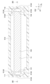
- FIG. 2 is a perspective view of the current sensor according to the first embodiment.
- FIG. 2 is a view taken along the line II in FIG. 1 .
- FIG. 2 is a view taken along the line III in FIG. 1 .
- FIG. 4 is a view taken along the line IV in FIG. 1 .
- FIG. 2 is a view taken along the line V in FIG. 1 .
- FIG. 6 is a view taken along line VI in FIG. 1 .
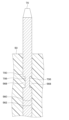
- FIG. 8 is an enlarged view of a portion VIII in FIG. 7 .
- FIG. 8 is an enlarged view of part X in FIG. FIG.
- FIG. 13 is an enlarged view of part XIII in FIG. 12 .
- FIG. 13 is an enlarged view of part XIV in FIG. 12 .
- FIG. 13 is an enlarged view of part XV in FIG. 12 .
- FIG. 5 is an enlarged view of a portion XVII in FIG. 4 .
- FIG. 2 is a view taken along the line XX in FIG. 1 .
- FIG. 13 is a perspective view showing deformations of a second extension portion and a fourth extension portion of the bus bar of the current sensor.
- FIG. FIG. 4 is a cross-sectional view showing the mounting of a substrate to a case of the current sensor.
- FIG. 4 is a cross-sectional view of a current sensor of a comparative example.
- FIG. 13 is a perspective view of a current sensor according to a second embodiment.
- FIG. 25 is a view taken along the arrow XXV in FIG. 24 .
- FIG. 13 is an external view of a current sensor according to a third embodiment. Enlarged view of part XXVII in Figure 26.
- FIG. 4 is an external view showing a state in which a bus bar of the current sensor is inserted into a case.
- FIG. 4 is an external view showing a state in which a bus bar of the current sensor is inserted into a case.
- FIG. 13 is an external view of a bus bar in a current sensor according to a modified example of the third embodiment.
- FIG. 13 is an external view of a bus bar in a current sensor according to a modified example of the third embodiment.
- FIG. 13 is an external view of a bus bar in a current sensor according to a modified example of the third embodiment.
- FIG. 13 is an external view of a current sensor according to a fourth embodiment.
- FIG. FIG. 13 is an external view of a current sensor according to a fifth embodiment.
- FIG. 4 is an enlarged cross-sectional view of the periphery of the bus bar of the current sensor.
- FIG. 13 is an external view of a current sensor according to a sixth embodiment.
- FIG. 13 is an enlarged cross-sectional view of the periphery of a core in a current sensor according to a seventh embodiment.
- FIG. 23 is an enlarged cross-sectional view of the periphery of a bus bar of the current sensor of the eighth embodiment.
- FIG. 13 is a cross-sectional view of a current sensor according to a ninth embodiment.
- FIG. 23 is an enlarged cross-sectional view of a substrate and a case of a current sensor according to a tenth embodiment.
- FIG. 23 is an enlarged cross-sectional view of a substrate and a case of a current sensor according to an eleventh embodiment.
- FIG. 23 is a cross-sectional view of the periphery of a terminal of a current sensor according to a twelfth embodiment.
- the current sensor of this embodiment is used, for example, in an inverter that drives a three-phase AC motor mounted on a vehicle (not shown).
- the current sensor 5 includes a bus bar 10, a core 20, a detection portion 30, lead wires 35, a substrate 40, a case 50, a resin filling portion 60, and a terminal 70.
- the busbars 10 are formed in a plate shape.
- the busbars 10 are made of copper or the like and are therefore conductive. If necessary, the surface of the busbars 10 is plated to prevent surface oxidation.
- the number of busbars 10 corresponds to the number of phases of the motor and inverter. In this example, the number of phases of the motor and inverter is three, so there are three busbars 10.
- the three busbars 10 are arranged at intervals in the width direction DW of the busbars 10.
- the busbar 10 has a current path portion 100, a fastening portion 102, a first side surface 111, a first extension portion 121, and a second extension portion 122.
- the busbar 10 further has a second side surface 112, a third extension portion 123, a fourth extension portion 124, a first busbar protrusion 131, and a second busbar protrusion 132.
- the current path portion 100 is formed in a plate shape.
- the fastening portions 102 are, for example, holes extending in the thickness direction DT, and are connected to each phase of the inverter. Therefore, current flows from each phase of the inverter through each current path portion 100.
- the longitudinal direction DL of the current path portion 100 will be simply referred to as the longitudinal direction DL.
- the width direction DW of the current path portion 100 will be simply referred to as the width direction DW.
- the thickness direction DT of the current path portion 100 will be simply referred to as the thickness direction DT.
- the first side surface 111 is a surface of the current path portion 100 that is perpendicular to the width direction DW and corresponds to a surface of the current path portion 100 that intersects with the width direction DW.
- the first extension portion 121 extends in the width direction DW from the area of the first side surface 111 where the current path portion 100 protrudes from the case 50 described below.
- the second extension portion 122 is connected to the side of the first extension portion 121 opposite the first side surface 111.
- the second extension portion 122 also extends from the first extension portion 121 in a direction intersecting the direction in which the first extension portion 121 extends, in this case, in the longitudinal direction DL. Furthermore, when the current path portion 100 undergoes elastic deformation, plastic deformation, or other deformation in the thickness direction DT, the second extension portion 122 deforms in the thickness direction DT while coming into contact with the case 50 described below.
- the length of the second extension 122 in the width direction DW is shorter than the length of the current path portion 100 in the width direction DW. Furthermore, the cross-sectional area of the second extension 122 when cut in a direction perpendicular to the longitudinal direction DL is smaller than the cross-sectional area of the current path portion 100 when cut in a direction perpendicular to the longitudinal direction DL. Therefore, the second extension 122 is more easily deformed than the current path portion 100.
- the second side 112 is located on the opposite side to the first side 111.
- the second side 112 is a surface of the current path portion 100 that is perpendicular to the width direction DW, and corresponds to a surface of the current path portion 100 that intersects with the width direction DW.
- the third extension portion 123 extends in the width direction DW from the area of the second side surface 112 where the current path portion 100 protrudes from the case 50 described below.
- the fourth extension 124 is connected to the side of the third extension 123 opposite the second side surface 112.
- the fourth extension 124 also extends from the third extension 123 in a direction intersecting the direction in which the third extension 123 extends, in this case, in the longitudinal direction DL. Furthermore, when the current path portion 100 undergoes elastic deformation, plastic deformation, or other deformation in the thickness direction DT, the fourth extension 124 deforms in the thickness direction DT while coming into contact with the case 50 described below.
- the length of the fourth extension 124 in the width direction DW is shorter than the length of the current path portion 100 in the width direction DW. Furthermore, the cross-sectional area of the fourth extension 124 when cut in a direction perpendicular to the longitudinal direction DL is smaller than the cross-sectional area of the current path portion 100 when cut in a direction perpendicular to the longitudinal direction DL. Therefore, the fourth extension 124 is more easily deformed than the current path portion 100.
- the first bus bar protrusion 131 protrudes in the width direction DW from the range of the first side surface 111 that is housed in the case 50 described below. Also, as shown in Fig. 16, the first bus bar protrusion 131 includes a first contact portion 1310 and a first inclined portion 1311.
- the first contact portion 1310 is a portion of the first bus bar protrusion 131 that is in contact with the case 50 described below.
- the first inclined portion 1311 is connected to the side of the first contact portion 1310 opposite the fastening portion 102. Furthermore, the first inclined portion 1311 is inclined in a direction such that the size of the first bus bar protrusion 131 decreases as it moves away from the boundary with the first contact portion 1310.
- the second bus bar protrusion 132 protrudes in the width direction DW from the range of the second side surface 112 that is housed in the case 50 described below. Also, as shown in Fig. 16, the second bus bar protrusion 132 includes a second contact portion 1320 and a second inclined portion 1321.
- the second contact portion 1320 is a portion of the second bus bar protrusion 132 that is in contact with the case 50 described below.
- the second inclined portion 1321 is connected to the side of the second contact portion 1320 opposite the fastening portion 102. Furthermore, the second inclined portion 1321 is inclined in a direction such that the size of the second bus bar protrusion 132 decreases as it moves away from the boundary with the second contact portion 1320.
- the core 20 is formed in a C-shape from a soft magnetic material such as permalloy or directional magnetic steel plate.
- the core 20 is formed, for example, by bending a plate-shaped soft magnetic material into a C-shape.
- the number of cores 20 corresponds to the number of bus bars 10.
- the number of bus bars 10 is three, so the number of cores 20 is three. Since the bus bars 10 are arranged at intervals in the width direction DW, the three cores 20 are arranged at intervals in the width direction DW.
- the magnetic field generated by the current flowing through each bus bar 10 passes through each core 20.
- the core 20 has a gap forming portion 21, a core side portion 22, a core bottom portion 23, a core hole 24, a core outer surface 25, and a core protrusion 26.
- the gap forming portion 21 is formed in a plate shape extending in the width direction DW. Furthermore, the lateral outer corner C_out_top, which is the corner of the gap forming portion 21 on the outer side in the width direction DW, is rounded.
- the gap forming portion 21 also includes a first end surface 211, a second end surface 212, and a gap 213.
- the first end face 211 faces in the width direction DW.
- the second end face 212 faces in the width direction DW and faces the first end face 211 in the width direction DW. Furthermore, when the first end face 211 is projected in the width direction DW, the second end face 212 overlaps with the projected first end face 211.
- the gap 213 is a space defined by the first end face 211 and the second end face 212. Furthermore, the gap 213 is connected to the outside of the core 20 and to the core hole 24 described below.
- the core horizontal portion 22 is connected to the gap forming portion 21.
- the core horizontal portion 22 extends in the thickness direction DT from the boundary between the core horizontal portion 22 and the gap forming portion 21.
- the lateral inner corner C_in_top which is the inner corner at the boundary between the core horizontal portion 22 and the gap forming portion 21, has an R-shape.
- the core horizontal portion 22 is separated from the current path portion 100 in the width direction DW.
- the core bottom 23 is connected to the core side portion 22. Furthermore, the core bottom 23 extends in the width direction DW. Furthermore, the bottom outer corner C_out_btm, which is the corner of the core bottom 23 on the outside in the width direction DW, is rounded. Furthermore, the bottom inner corner C_in_btm, which is the inner corner at the boundary between the core bottom 23 and the core side portion 22, is rounded. Furthermore, the core bottom 23 is separated from the current path portion 100 in the thickness direction DT.
- the core holes 24 are formed by the gap forming portion 21, the core side portion 22, and the core bottom portion 23. Furthermore, a portion of each bus bar 10 is inserted into the space of each core hole 24.
- the core outer surface 25 is the outer surface of the gap forming portion 21, and is the surface of the gap forming portion 21 that faces outward in the thickness direction DT.
- the passing surface St is a surface that passes through the inner edge of the core horizontal portion 22 extending in the thickness direction DT and is perpendicular to the width direction DW.
- the passing surface St is aligned in the width direction DW.
- the core protrusions 26 protrude in the thickness direction DT from the area between adjacent passing surfaces St on the core outer surface 25.
- the number of core protrusions 26 is two, but is not limited to this.
- the number of core protrusions 26 may be at least one.
- the shape of the core protrusions 26 is a quadrangular prism, but is not limited to this.
- the shape of the core protrusions 26 may be, for example, a polygonal prism or a cylinder.
- the detection unit 30 is disposed in the gap 213. Therefore, when the first end face 211 is projected in the width direction DW, the detection unit 30 overlaps with the projected first end face 211. Furthermore, when the second end face 212 is projected in the width direction DW, the detection unit 30 overlaps with the projected second end face 212. Furthermore, the detection unit 30 includes a detection element 31 and an IC (not shown), etc. Note that IC is an abbreviation for Integrated Circuit.
- the detection element 31 is a Hall element, a TMR element, a GMR element, an AMR element, etc. Furthermore, the detection element 31 detects the strength of the magnetic field in the width direction DW. Furthermore, the detection element 31 outputs a signal corresponding to the strength of the detected magnetic field, for example, a voltage corresponding to the strength of the detected magnetic field, to the outside.
- TMR is an abbreviation for Tunnel Magneto Resistive.
- GMR is an abbreviation for Giant Magneto Resistive.
- AMR is an abbreviation for Anisotropic Magneto Resistive.
- the lead wires 35 are connected to the detection unit 30.
- the board 40 is a printed circuit board. As shown in FIG. 7, the board 40 is connected to the lead wires 35 by soldering or the like. Furthermore, as shown in FIG. 4, FIG. 17, FIG. 18, and FIG. 19, the board 40 has a board side surface 400, a board recess 402, and a board hole 404.
- the substrate side surface 400 is a surface perpendicular to the longitudinal direction DL or width direction DW, and corresponds to a surface intersecting the longitudinal direction DL or width direction DW.
- the substrate side surface 400 is a surface intersecting the longitudinal direction DL or width direction DW.
- the thickness direction of the substrate 40 is not limited to coincide with the thickness direction DT of the current path section 100.
- the thickness direction of the substrate 40 may coincide with the longitudinal direction DL of the current path section 100, for example.
- the substrate side surface 400 corresponds to a surface intersecting the thickness direction DT or width direction DW.
- the substrate recess 402 is recessed from the substrate side surface 400, and here, recessed in the longitudinal direction DL from the substrate side surface 400 perpendicular to the longitudinal direction DL.
- the substrate recess 402 is formed in an arc shape.
- the substrate recess 402 may be recessed in the width direction DW from the substrate side surface 400 perpendicular to the width direction DW.
- the shape of the substrate recess 402 is an elliptical arc shape.
- the shape of the substrate recess 402 is not limited to an elliptical arc shape.
- the shape of the substrate recess 402 may be a polygonal shape, an arc shape, an elliptical arc shape, or the like.
- the number of substrate recesses 402 is three, but is not limited to this.
- the number of substrate recesses 402 needs to be at least one, and it is preferable that the number is three or more, so that a plane is formed by straight lines connecting the substrate recesses 402.
- the substrate hole 404 is a through hole penetrating the inside of the substrate 40 in the thickness direction DT.
- the shape of the substrate hole 404 is cylindrical.
- the shape of the substrate hole 404 is not limited to being cylindrical.
- the shape of the substrate hole 404 may be a polygonal column or an elliptical column.
- the number of substrate holes 404 is four, but is not limited to this.
- the number of substrate holes 404 may be at least one, and it is preferable that the number of substrate holes 404 is three or more, so that a plane is formed by straight lines connecting the substrate holes 404.
- the substrate hole 404 penetrates the inside of the substrate 40 in the thickness direction DT.
- the thickness direction of the substrate 40 is not limited to coincide with the thickness direction DT of the current path portion 100.
- the thickness direction of the substrate 40 may coincide with the longitudinal direction DL of the current path portion 100, for example. In this case, the substrate hole 404 penetrates the inside of the substrate 40 in the longitudinal direction DL.
- the case 50 is formed by injection molding using a thermoplastic resin such as polybutylene terephthalate.
- the case 50 also houses the busbar 10, the core 20, the detection section 30, the lead wires 35, the substrate 40, the resin filling section 60 described below, and the terminals 70.
- the busbar 10, the core 20, etc. are aligned in the width direction DW, so the length of the case 50 in the width direction DW is longer than the length of the case 50 in the longitudinal direction DL.
- the case 50 also has a collar 500, a core storage chamber 502, a partition 504, a case facing surface 506, a case protrusion 508, and a board storage chamber 510.
- the case 50 also has an opening 512, a first inner surface 521, a first hole 531, a first protrusion 541, a second inner surface 522, a second hole 532, and a second protrusion 542.
- the case 50 also has a storage chamber facing surface 548, a board recess 550, and a board protrusion 552.
- the case 50 also has a terminal hole 560, a terminal inner surface 562, a terminal recess 564, and a terminal protrusion 566.
- the case 50 also has a liquid drain recess 570 and a liquid discharge portion 580.
- the collar 500 is formed into a ring shape from metal or the like. Furthermore, a shaft or the like (not shown) is inserted into the collar 500, thereby connecting the case 50 to the outside of the current sensor 5. This fixes the current sensor 5 to its outside.
- the cores 20 are accommodated in the space of the core accommodating chamber 502.
- the partition section 504 is formed between adjacent cores 20 and is formed in a plate shape extending in the longitudinal direction DL and thickness direction DT. This separates adjacent core accommodating chambers 502.
- the case facing surface 506 is the surface of the inner surface forming the core accommodating chamber 502 that faces the core 20 in the longitudinal direction DL.
- the case protrusion 508 protrudes from the inner surface forming the core accommodating chamber 502 toward the core 20.
- the case protrusion 508 protrudes from the case facing surface 506 in the longitudinal direction DL.
- the case protrusion 508 is in contact with the core 20. This makes it easier to position the case 50 and the core 20.
- a space is formed between the case facing surface 506 and the core 20.
- the number of case protrusions 508 is four as shown in FIG. 8, but is not limited to this.
- the number of case protrusions 508 needs to be at least one, and it is preferable that the number is three or more, so that a plane is formed by straight lines connecting the case protrusions 508.
- the shape of the case protrusion 508 is cylindrical.
- the shape of the case protrusion 508 is not limited to a cylindrical shape.
- the shape of the case protrusion 508 may be, for example, a polygonal prism shape or an elliptical prism shape.
- the space of the substrate accommodating chamber 510 accommodates the detection unit 30, the lead wires 35, and the substrate 40. Furthermore, since the detection unit 30 is disposed in the gap 213, the substrate accommodating chamber 510 is formed on the gap 213 side of the case 50.
- a portion of the opening 512 is inserted into the core hole 24, as shown in Figures 2, 3, 7, and 8.
- a portion of the current path portion 100 is inserted into the space of the opening 512.
- the shape of the opening 512 is a polygonal tube here.
- the shape of the opening 512 is not limited to being a polygonal tube.
- the shape of the opening 512 may be a cylinder, etc.
- the opening 512 includes an opening surface 5120 and an opening protrusion 5122, as shown in Figures 12, 15 and 16.
- the opening surface 5120 faces the current path portion 100 in the width direction DW and the thickness direction DT.
- the opening protrusion 5122 protrudes from the opening surface 5120 toward the current path portion 100, and is in contact with the first bus bar protrusion 131 and the second bus bar protrusion 132.
- the opening protrusion 5122 protrudes from the opening surface 5120 in the thickness direction DT.
- the opening protrusion 5122 is in contact with the first bus bar protrusion 131 and the second bus bar protrusion 132 in the thickness direction DT.
- the opening protrusion 5122 protrudes from the opening surface 5120 in the width direction DW.
- the opening protrusion 5122 is in contact with the first bus bar protrusion 131 and the second bus bar protrusion 132 in the width direction DW. This allows the case 50 and the bus bar 10 to be positioned. Furthermore, a space is formed between the opening surface 5120 and the current path portion 100.
- the shape of the opening protrusion 5122 is a triangular prism.
- the shape of the opening protrusion 5122 is not limited to a triangular prism.
- the shape of the opening protrusion 5122 may be, for example, a polygonal prism or a cylinder.
- the Young's modulus of the opening protrusion 5122 is smaller than the Young's modulus of the first bus bar protrusion 131 and the second bus bar protrusion 132. This makes the opening protrusion 5122 more easily deformable than the first bus bar protrusion 131 and the second bus bar protrusion 132.
- the Young's modulus of the opening protrusion 5122 is estimated, for example, from the Young's modulus of the material of the case 50.
- the Young's modulus of the first bus bar protrusion 131 and the second bus bar protrusion 132 is estimated, for example, from the Young's modulus of the material of the bus bar 10.
- the opening protrusion 5122 includes a protrusion contact portion 5124 and a protrusion inclined portion 5126.
- the protrusion contact portion 5124 is a portion of the opening protrusion 5122 that is in contact with the first bus bar protrusion 131 and the second bus bar protrusion 132.
- the protrusion inclined portion 5126 is connected to the fastening portion 102 side of the protrusion contact portion 5124. Furthermore, the protrusion inclined portion 5126 is inclined in a direction such that the size of the opening protrusion 5122 decreases as it moves away from the boundary with the protrusion contact portion 5124.
- the first inner surface 521 forms a first hole 531 as shown in Figures 11, 12, and 13.
- at least a portion of the second extension portion 122 is inserted into the space of the first hole 531. Therefore, the first inner surface 521 faces the second extension portion 122 in the width direction DW and thickness direction DT.
- the first protrusion 541 protrudes from the first inner surface 521 toward the second extension portion 122, and thus contacts the second extension portion 122. Specifically, the first protrusion 541 protrudes in the thickness direction DT from a portion of the first inner surface 521 that faces the second extension portion 122 in the thickness direction DT. As a result, the first protrusion 541 contacts the second extension portion 122 in the thickness direction DT. Also, the first protrusion 541 protrudes in the width direction DW from a portion of the first inner surface 521 that faces the second extension portion 122 in the width direction DW. As a result, the first protrusion 541 contacts the second extension portion 122 in the width direction DW.
- the shape of the first protrusion 541 is a triangular prism shape.
- the shape of the first protrusion 541 is not limited to a triangular prism shape.
- the shape of the first protrusion 541 may be, for example, a polygonal prism shape, a cylindrical shape, etc.
- the second inner surface 522 forms a second hole 532, as shown in Figures 11, 12, and 14.
- the fourth extension portion 124 is inserted into the space of the second hole 532. Therefore, the second inner surface 522 faces the fourth extension portion 124 in the width direction DW and thickness direction DT.
- the second protrusion 542 protrudes from the second inner surface 522 toward the fourth extension portion 124, and thus contacts the fourth extension portion 124. Specifically, the second protrusion 542 protrudes in the thickness direction DT from a portion of the second inner surface 522 that faces the fourth extension portion 124 in the thickness direction DT. As a result, the second protrusion 542 contacts the fourth extension portion 124 in the thickness direction DT. Also, the second protrusion 542 protrudes in the width direction DW from a portion of the second inner surface 522 that faces the fourth extension portion 124 in the width direction DW. As a result, the second protrusion 542 contacts the fourth extension portion 124 in the width direction DW.
- the shape of the second protrusion 542 is a triangular prism shape.
- the shape of the second protrusion 542 is not limited to a triangular prism shape.
- the shape of the second protrusion 542 may be, for example, a polygonal prism shape, a cylindrical shape, etc.
- the chamber-facing surface 548 is a surface that forms the substrate chamber 510 and faces the substrate 40 in the thickness direction DT.
- the chamber-facing surface 548 faces the substrate 40 in the thickness direction DT.
- the thickness direction of the substrate 40 is not limited to coincide with the thickness direction DT of the current path section 100.
- the thickness direction of the substrate 40 may coincide with the longitudinal direction DL of the current path section 100, for example. In this case, the chamber-facing surface 548 faces the substrate 40 in the longitudinal direction DL.
- the recesses 550 for the board are recessed in the thickness direction DT from the chamber-facing surface 548. Furthermore, the recesses 550 for the board are formed at positions corresponding to the recesses 402 for the board. As a result, the recesses 550 for the board are connected to the recesses 402 in the thickness direction DT. Furthermore, the number of recesses 550 for the board is the same as the number of recesses 402 for the board. For this reason, it is preferable that a plane is formed by straight lines connecting the recesses 550 for the board, similar to the recesses 402 for the board.
- the board protrusions 552 protrude from the chamber-facing surface 548 towards the board hole 404.
- the board protrusions 552 protrude in the thickness direction DT from the chamber-facing surface 548.
- a portion of the board protrusions 552 is inserted into the board hole 404.
- the number of board protrusions 552 is the same as the number of board holes 404. For this reason, it is preferable that a plane is formed by straight lines connecting the board protrusions 552 together, similar to the board holes 404.
- the board protrusion 552 includes a protrusion side surface 5520 and a board flange 5522.
- the protrusion side surface 5520 is a surface of the board protrusion 552 that extends in the direction in which the board protrusion 552 extends, in this case, the surface that extends in the thickness direction DT.
- the board flange 5522 extends from the protrusion side surface 5520 in a direction perpendicular to the direction in which the board protrusion 552 extends, in this case, the thickness direction DT.
- the board 40 is disposed between the board flange 5522 and the storage chamber facing surface 548. Furthermore, the board 40 and the board flange 5522 are in contact with each other by being thermally caulked or the like. This restricts the movement of the board 40.
- the terminal hole 560 is a space into which the terminal 70 described below is inserted, as shown in Figures 7 and 10.
- the terminal inner surface 562 forms a terminal hole 560.
- the terminal inner surface 562 faces the terminal side surface 700 described below in a direction perpendicular to the direction in which the terminal 70 described below extends, in this case, a direction perpendicular to the thickness direction DT.
- the terminal recess 564 is recessed in the direction in which the terminal flange 702 (described below) extends from the terminal inner surface 562, which in this case is the width direction DW. Furthermore, the terminal recess 564 is in contact with the terminal flange 702 (described below). As a result, the terminal recess 564 restricts the movement of the terminal 70 (described below).
- the terminal protrusion 566 protrudes from the terminal inner surface 562 in the direction in which the terminal hole 704 described below extends, in this case in the longitudinal direction DL.
- the terminal protrusion 566 is inserted into the terminal hole 704. This brings the terminal protrusion 566 into contact with the terminal flange 702. Therefore, the terminal protrusion 566 restricts the movement of the terminal 70.
- the liquid drain recess 570 accommodates a portion of the terminal 70, as shown in Figures 1, 5, and 20.
- the liquid drain recess 570 also includes a recess bottom surface 572 and a recess side surface 574, as shown in Figure 20.
- the recess bottom surface 572 is a surface that is perpendicular to the thickness direction DT and corresponds to a surface that intersects with the thickness direction DT. Furthermore, the recess bottom surface 572 is located on the side of the case 50 opposite the substrate 40. Also, a portion of the recess bottom surface 572 is formed in a stepped shape.
- the recess side surface 574 extends in the thickness direction DT from the recess bottom surface 572. As a result, the recess side surface 574 and the recess bottom surface 572 form a space for the liquid draining recess 570.
- the liquid discharge portion 580 is a groove or hole that communicates with the space of the liquid drain recess 570 and the outside of the case 50, and here, penetrates the recess side surface 574 in the width direction DW.
- the liquid discharge portion 580 also discharges liquid such as water that flows into the liquid drain recess 570 to the outside of the case 50.
- the liquid discharge portion 580 penetrates the recess side surface 574 in the width direction DW, it is not limited to this.
- the liquid discharge portion 580 may, for example, penetrate the recess side surface 574 in the longitudinal direction DL.
- the resin filling section 60 is formed between the inner surface forming the core accommodating chamber 502 and the surface of the core 20 by filling the resin, such as urethane, by insert molding or the like.
- the resin filling section 60 is also formed between the surface of the core 20 and the surface of the partition section 504 that faces the core 20 in the width direction DW. As a result, the resin filling section 60 covers the core 20 and fixes the core 20 and the case 50.
- the case protrusion 508 forms a space between the case facing surface 506 and the surface of the core 20 that faces the case facing surface 506 in the longitudinal direction DL.
- the resin filling portion 60 is formed in this space and is connected to the case facing surface 506 and the surface of the core 20 that faces the case facing surface 506 in the longitudinal direction DL. This increases the contact area between the core 20 and case 50 and the resin filling portion 60 compared to when the case facing surface 506 and the core 20 are in contact or in close contact. This increases the force that fastens the case 50 and the core 20.
- the resin filling portion 60 covers the core surface 27 and also covers the partition portion 504.
- the size of the resin filling portion 60 covering the core 20 is larger than when the resin filling portion 60 does not cover the partition portion 504. This prevents the core 20 from being exposed to the outside.
- the core surface 27 is the surface of the core 20 opposite the case facing surface 506.
- a plurality of terminals 70 are formed.
- the terminals 70 are arranged at intervals in the longitudinal direction DL.
- the terminals 70 are also arranged at intervals in the direction of the current flowing through the busbar 10. Note that here, as will be described later, the longitudinal direction DL and the direction of the current flowing through the busbar 10 coincide with each other.
- a portion of the terminal 70 is inserted into a through hole in the substrate 40 and is connected to the substrate 40 by soldering or the like. As a result, the terminal 70 is connected to the detection unit 30 via the lead wire 35. Therefore, the terminal 70 outputs a signal from the detection element 31 to an external device such as a computing device (not shown). Furthermore, the terminal 70 is connected to a component (not shown) arranged on the substrate 40.
- the terminal 70 extends from the substrate 40 in the thickness direction DT.
- a portion of the terminal 70 is housed in the liquid drainage recess 570 as shown in FIG. 1 and FIG. 20.
- the terminal 70 protrudes from the step portion of the bottom surface 572 of the recess.
- the thickness direction of the substrate 40 coincides with the thickness direction DT of the current path portion 100
- the terminal 70 extends from the substrate 40 in the thickness direction DT.
- the thickness direction of the substrate 40 is not limited to coincide with the thickness direction DT of the current path portion 100.
- the thickness direction of the substrate 40 may coincide with the longitudinal direction DL of the current path portion 100, for example. In this case, the terminal 70 extends from the substrate 40 in the longitudinal direction DL.
- the terminal 70 includes a terminal side surface 700, a terminal flange portion 702, and a terminal hole 704.
- the terminal side surface 700 extends in the direction in which the terminal 70 extends, here in the thickness direction DT.
- the terminal flange portion 702 extends from the terminal side surface 700 in a direction perpendicular to the thickness direction DT, here in the width direction DW. Furthermore, the terminal flange portion 702 and the terminal recess 564 are in contact with each other. This restricts the movement of the terminal 70.
- the terminal 70 is also formed symmetrically in the direction in which the terminal 70 extends, here in the thickness direction DT, with the terminal flange portion 702 at the center. Furthermore, the terminal flange portion 702 includes an exposed portion 7020. The exposed portion 7020 is exposed to the outside by being exposed from the terminal recess 564.
- the terminal hole 704 is surrounded by the terminal flange 702 and is a through hole or bottomed hole that extends in a direction perpendicular to the direction in which the terminal flange 702 extends, in this case, in the longitudinal direction DL.
- the terminal protrusion 566 is inserted into the terminal hole 704. This restricts the movement of the terminal 70.
- the current sensor 5 of the first embodiment is configured as described above. Next, current detection by the current sensor 5 will be explained.
- the current path portion 100 of the busbar 10 extends in the longitudinal direction DL and is connected to an inverter (not shown). Therefore, an AC current from the inverter flows through the current path portion 100.
- the direction of the current flowing through the current path portion 100 is the longitudinal direction DL.
- the AC current flowing through the current path portion 100 generates a circumferential magnetic field centered on an axis that passes through the current path portion 100 and extends in the longitudinal direction DL.
- This generated magnetic field causes magnetic lines to pass through the core 20 and therefore pass through the gap 213. Therefore, these magnetic lines pass through the detection element 31. Therefore, the detection element 31 detects the strength of the magnetic field in the width direction DW.
- the detection element 31 detects the AC current from the inverter.
- the detection element 31 also outputs a signal corresponding to the strength of the detected magnetic field to an external device such as a computing device (not shown) via the lead wire 35, the substrate 40, and the terminal 70.
- This calculation device then calculates the AC current from the inverter based on the signal from the detection element 31.
- the current sensor 5 detects the current. Next, we will explain how the current sensor 5 prevents damage to the case 50.
- the busbar 10 has a first side surface 111, a first extension portion 121, a second extension portion 122, a second side surface 112, a third extension portion 123, and a fourth extension portion 124, as shown in FIG. 11 etc.
- the first side surface 111 is a surface of the current path portion 100 that intersects with the width direction DW.
- the first extension portion 121 extends in the width direction DW from a range of the first side surface 111 where the current path portion 100 protrudes from the case 50.
- the second extension portion 122 is connected to the first extension portion 121 and extends in a direction that intersects with the direction in which the first extension portion 121 extends.
- the second extension portion 122 deforms in the thickness direction DT while coming into contact with the case 50.
- the second extension portion 122 is subjected to stress due to the force received from the case 50 in addition to stress due to deformation of the current path portion 100.
- the second extension portion 122 is more likely to deform in the thickness direction DT than the current path portion 100. Therefore, for example, as shown in FIG.
- the second extension portion 122 deforms in the thickness direction DT to a greater extent than the deformation amount of the current path portion 100.
- the second side surface 112 is a surface of the current path portion 100 that is located on the opposite side to the first side surface 111 and intersects with the width direction DW.
- the third extension portion 123 extends in the width direction DW from a range of a portion of the second side surface 112 where the current path portion 100 protrudes from the case 50.
- the fourth extension 124 is connected to the third extension 123 and extends in a direction intersecting the direction in which the third extension 123 extends.
- the fourth extension 124 deforms in the thickness direction DT while contacting the case 50.
- the fourth extension 124 is subjected to stress due to the force received from the case 50 in addition to stress due to deformation of the current path portion 100. Therefore, when the current path portion 100 deforms in the thickness direction DT, the fourth extension 124 is more likely to deform in the thickness direction DT than the current path portion 100. Therefore, for example, when the current path portion 100 deforms in the thickness direction DT, the fourth extension 124 deforms in the thickness direction DT to a degree greater than the deformation amount of the current path portion 100.
- the second extension 122 and the fourth extension 124 are easily deformed, they are likely to absorb the stress energy generated by the deformation of the busbar 10 when connecting the busbar 10 to a detection target such as an inverter (not shown). This reduces the stress applied to the case 50 that houses a part of the busbar 10, the core 20, and the detection element 31. This prevents the case 50 from being damaged.
- the current sensor 5 also provides the following advantages:
- the case 50 has a first inner surface 521, a first hole 531, a first protrusion 541, a second inner surface 522, a second hole 532, and a second protrusion 542.
- the first inner surface 521 forms the first hole 531.
- At least a part of the second extension 122 is inserted into the space of the first hole 531.
- the first inner surface 521 faces the second extension 122 in the width direction DW and the thickness direction DT.
- the first protrusion 541 protrudes from the first inner surface 521 toward the second extension 122, thereby contacting the second extension 122.
- the second inner surface 522 forms a second hole 532.
- At least a part of the fourth extension 124 is inserted into the space of the second hole 532.
- the second inner surface 522 faces the fourth extension 124 in the width direction DW and the thickness direction DT.
- the second protrusion 542 protrudes from the second inner surface 522 toward the fourth extension portion 124, thereby making
- the cross-sectional area of the second extension 122 when cut in a direction perpendicular to the longitudinal direction DL is smaller than the cross-sectional area of the current path portion 100 when cut in a direction perpendicular to the longitudinal direction DL.
- the length of the second extension 122 in the width direction DW is shorter than the length of the current path portion 100 in the width direction DW.
- the cross-sectional area of the fourth extension 124 when cut in a direction perpendicular to the longitudinal direction DL is smaller than the cross-sectional area of the current path portion 100 when cut in a direction perpendicular to the longitudinal direction DL.
- the length of the fourth extension 124 in the width direction DW is shorter than the length of the current path portion 100 in the width direction DW.
- the second extension portion 122 and the fourth extension portion 124 are more easily deformed than the current path portion 100. Therefore, they are more likely to absorb the stress energy generated by the deformation of the busbar 10 when connecting the busbar 10 to a detection target such as an inverter (not shown). This reduces the stress applied to the case 50 that houses a part of the busbar 10, the core 20, and the detection element 31. This suppresses damage to the case 50.
- the case of a current sensor as described in Patent Document 1 is subjected to stress due to forces from outside the case, such as forces generated when connecting the bus bar to a detection target such as an inverter, and heat generated by current flowing through the bus bar.
- forces from outside the case such as forces generated when connecting the bus bar to a detection target such as an inverter, and heat generated by current flowing through the bus bar.
- the stress applied to the case makes it prone to deformation, such as warping.
- the case 50 has a core accommodating chamber 502 and a partition section 504.
- the core accommodating chambers 502 correspond to the first and second accommodating chambers, and each accommodates two cores 20.
- the partition section 504 separates adjacent core accommodating chambers 502.
- the bus bar 10 corresponds to the first and second bus bars.
- the cores 20 correspond to the first and second cores.
- the detection element 31 corresponds to the first and second detection elements.
- the partition 504 reinforces the core chamber 502. This improves the rigidity of the case 50 compared to a case in which the partition 504 is not formed. This reduces deformation of the case 50, such as warping.
- the current sensor 5 includes a resin-filled portion 60.
- the resin-filled portion 60 corresponds to the first resin portion and the second resin portion, and is formed of resin between the inner surface that forms the core accommodating chamber 502 and the surface of the core 20.
- the resin-filled portion 60 is connected to the inner surface that forms the core accommodating chamber 502 and the surface of the core 20, and covers the core 20. This fixes the core 20 and the case 50.
- the resin used for the resin-filled portion 60 is urethane or the like, the material cost is relatively high.
- the partition portion 504 is formed, and therefore the size of the resin-filled portion 60 is smaller by the size of the partition portion 504 compared to a case in which the partition portion 504 is not formed. As a result, the amount of resin such as urethane used is reduced, and the cost of the current sensor 5 is reduced.
- the case 50 has a case facing surface 506.
- the case facing surface 506 is a surface of the inner surface forming the core accommodating chamber 502 that faces the core 20 in the longitudinal direction DL.
- the core 20 has a core surface 27.
- the core surface 27 is the surface of the core 20 opposite the case facing surface 506.
- the resin-filled portions 60 cover the core surface 27 and also cover the partition portions 504, thereby connecting adjacent resin-filled portions 60 to each other.
- the case facing surface 506 corresponds to the first facing surface and the second facing surface.
- the core surface 27 corresponds to the first core surface and the second core surface.
- the size of the resin-filled portion 60 covering the core 20 becomes larger than when the partition portion 504 is not covered. This prevents the core 20 from being exposed to the outside.
- the case 50 has a case facing surface 506 and a case protrusion 508.
- the case facing surface 506 is a surface of the inner surface forming the core accommodating chamber 502 that faces the core 20 in the longitudinal direction DL.
- the case protrusion 508 protrudes from the case facing surface 506 in the longitudinal direction DL, thereby forming a space between the case facing surface 506 and the surface of the core 20 that faces the case facing surface 506 in the longitudinal direction DL.
- the resin filling portion 60 is formed of resin between the inner surface forming the core accommodating chamber 502 and the surface of the core 20, and is connected to the inner surface forming the core accommodating chamber 502 and the surface of the core 20, and covers the core 20.
- the resin filling portion 60 is also formed between the case facing surface 506 and the surface of the core 20 that faces the case facing surface 506 in the longitudinal direction DL. As a result, the resin filling portion 60 is connected to the case facing surface 506 and the surface of the core 20 that faces the case facing surface 506 in the longitudinal direction DL.
- the case protrusion 508 forms a space between the case facing surface 506 and the surface of the core 20 that faces the case facing surface 506 in the longitudinal direction DL. Since the resin filling portion 60 is formed in this space, the contact area between the core 20 and the case 50 and the resin filling portion 60 is larger than when the case facing surface 506 and the core 20 are in contact or in close contact. This increases the force with which the resin filling portion 60 fixes the core 20 and the case 50. This suppresses misalignment of the core 20 relative to the case 50, thereby suppressing misalignment of the busbar 10 and the detection element 31 relative to the core 20. This suppresses a decrease in the accuracy of detection of the magnetic field strength by the detection element 31. This suppresses a decrease in the accuracy of current detection.
- the case 50 has a case protrusion 508.
- the case protrusion 508 protrudes from the inner surface that forms the core accommodating chamber 502 toward the core 20, thereby making contact with the core 20.
- the case protrusion 508 protrudes from the case facing surface 506 in the longitudinal direction DL, thereby making contact with the core 20 in the longitudinal direction DL.
- the case 50 has an opening 512.
- the opening 512 is inserted into the core hole 24 and the bus bar 10 is inserted into the opening 512.
- the bus bar 10 also has a first bus bar protrusion 131 and a second bus bar protrusion 132.
- the first bus bar protrusion 131 protrudes from the first side surface 111 toward the opening 512, thereby making contact with the opening 512.
- the second bus bar protrusion 132 protrudes from the second side surface 112 toward the opening 512, thereby making contact with the opening 512.
- a space is formed between the opening 512 and the first bus bar protrusion 131 and the second bus bar protrusion 132.
- the first side surface 111 and the second side surface 112 correspond to the surfaces facing the opening 512.
- heat generated by the busbar 10 is less likely to be transferred to the case 50. This prevents damage to the case 50. Also, heat is less likely to be transferred from the case 50 to the detection element 31. This prevents heat from being transferred to the detection element 31. This prevents changes in the characteristics and failure of the detection element 31.
- the first bus bar projection 131 includes a first contact portion 1310 and a first inclined portion 1311.
- the first contact portion 1310 is in contact with the opening 512.
- the first inclined portion 1311 is connected to the first contact portion 1310 and is inclined in a direction in which the size of the first bus bar projection 131 decreases as it moves away from the boundary with the first contact portion 1310.
- the second bus bar projection 132 includes a second contact portion 1320 and a second inclined portion 1321.
- the second contact portion 1320 is in contact with the opening 512.
- the second inclined portion 1321 is connected to the second contact portion 1320 and is inclined in a direction in which the size of the second bus bar projection 132 decreases as it moves away from the boundary with the second contact portion 1320.
- the bus bar 10 when the bus bar 10 is inserted into the space of the opening 512, the bus bar 10 is guided by the first inclined portion 1311 and the second inclined portion 1321. This makes it easier for the bus bar 10 to be inserted into the space of the opening 512. This also reduces wear caused by contact between the first bus bar protrusions 131 and the second bus bar protrusions 132 and the opening 512. This prevents wear powder caused by contact between the first bus bar protrusions 131 and the second bus bar protrusions 132 and the opening 512 from entering the fastening portion 102. This prevents damage to the bus bar 10 caused by wear powder getting caught when connecting the fastening portion 102 to a detection target such as an inverter (not shown).
- a detection target such as an inverter (not shown).
- the opening 512 includes an opening surface 5120 and an opening protrusion 5122.
- the opening surface 5120 faces the bus bar 10.
- the opening protrusion 5122 protrudes from the opening surface 5120 toward the first bus bar protrusion 131 and the second bus bar protrusion 132, and is in contact with the first bus bar protrusion 131 and the second bus bar protrusion 132.
- the size of the space between the opening 512 and the first and second bus bar protrusions 131 and 132 is larger. This makes it difficult for heat generated by the bus bar 10 to be transferred to the case 50. This makes it difficult for heat to be transferred from the case 50 to the detection element 31. This prevents heat from being transferred to the detection element 31, thereby preventing changes in the characteristics and failure of the detection element 31.
- the Young's modulus of the opening protrusion 5122 is smaller than the Young's modulus of the first bus bar protrusion 131 and the second bus bar protrusion 132.
- the opening protrusion 5122 is more easily deformed than the first bus bar protrusion 131 and the second bus bar protrusion 132, and therefore more easily absorbs stress energy generated by deformation of the bus bar 10 when connecting the bus bar 10 to a detection target such as an inverter (not shown).
- a detection target such as an inverter (not shown).
- the opening protrusion 5122 includes a protrusion contact portion 5124 and a protrusion inclined portion 5126.
- the protrusion contact portion 5124 is in contact with the first bus bar protrusion 131 and the second bus bar protrusion 132.
- the protrusion inclined portion 5126 is connected to the protrusion contact portion 5124, and is inclined in a direction such that the size of the opening protrusion 5122 decreases as it moves away from the boundary with the protrusion contact portion 5124.
- the printed circuit board to which the sensor chip is connected may be housed in a case.
- the position of the printed circuit board if the position of the printed circuit board is shifted relative to the case, the position of the sensor chip will also shift relative to the case. Furthermore, if the position of the sensor chip is shifted, the positions of the core and bus bar will shift relative to the sensor chip. This reduces the accuracy of the sensor chip in detecting the strength of the magnetic field due to fluctuations in the magnetic field and changes in the detection position of the magnetic field strength. Therefore, at this time, the accuracy of current detection decreases.
- the board 40 has a board side surface 400 and a board recess 402.
- the board recess 402 is recessed from the board side surface 400.
- the case 50 also has a board accommodation chamber 510, an accommodation chamber facing surface 548, and a board recess 550.
- the board accommodation chamber 510 accommodates the board 40.
- the accommodation chamber facing surface 548 is a surface that forms the board accommodation chamber 510 and faces the board 40.
- the board recess 550 corresponds to a case recess and is recessed from the accommodation chamber facing surface 548.
- the board recess 550 is formed at a position corresponding to the board recess 402, and is thereby in communication with the board recess 402.
- the board recess 402 and the board recess 550 can be used as markers, making it easier to position the board 40 and the case 50 compared to when the board recess 402 and the board recess 550 are not formed.
- a jig X such as a pin
- the board recess 402 by fitting a jig X such as a pin into the board recess 550 and having this jig X guide the board recess 402, the board 40 and the case 50 can be easily attached and the board 40 and the case 50 can be easily positioned.
- Three or more substrate recesses 402 and substrate recesses 550 are formed.
- a plane is formed by straight lines connecting the substrate recesses 402, and a plane is formed by straight lines connecting the substrate recesses 550.
- a printed circuit board with a sensor chip connected thereto may be housed in a case.
- the position of the sensor chip will also shift relative to the case.
- the positions of the core and bus bar will shift relative to the sensor chip. This causes the magnetic field fluctuation and the change in the detection position of the magnetic field strength to decrease the detection accuracy of the magnetic field strength by the sensor chip. Therefore, at this time, the current detection accuracy decreases.
- the substrate 40 has a substrate hole 404.
- the substrate hole 404 penetrates the inside of the substrate 40.
- the case 50 also has a substrate accommodating chamber 510, an accommodating chamber facing surface 548, and a substrate convex portion 552.
- the substrate accommodating chamber 510 accommodates the substrate 40 as described above.
- the accommodating chamber facing surface 548 is a surface that forms the substrate accommodating chamber 510 as described above, and faces the substrate 40.
- the substrate convex portion 552 corresponds to the case convex portion, and protrudes from the accommodating chamber facing surface 548 toward the substrate hole 404 and is inserted into the substrate hole 404.
- the substrate convex portion 552 also includes a convex portion side surface 5520 and a substrate flange portion 5522.
- the convex portion side surface 5520 extends in the direction in which the substrate convex portion 552 extends, which is the thickness direction DT in this case.
- the board flange 5522 corresponds to the case flange, and extends from the convex side surface 5520 in a direction perpendicular to the direction in which the board protrusion 552 extends, in this case, perpendicular to the thickness direction DT.
- the board 40 is disposed between the board flange 5522 and the storage chamber facing surface 548, and the board 40 and the board flange 5522 are in contact with each other, thereby restricting the movement of the board 40.
- the case of the current sensor as described in Patent Document 1 is subjected to stress due to external forces such as those generated when connecting the bus bar to a detection target such as an inverter, and heat generated by the current flowing through the bus bar.
- the two bus bars are arranged in the width direction, the length of the case in the width direction is longer than the length of the case in the longitudinal direction. Therefore, the amount of warping of the case in the width direction, for example, the amount of deflection, is greater than the amount of warping of the case in the longitudinal direction.
- multiple connection terminals are arranged at intervals in the width direction.
- connection terminals are easily displaced, making it difficult to connect the connection terminals to an external device. As a result, poor connection between the connection terminals and the external device is likely to occur.
- the length of the case 50 in the width direction DW is longer than the length of the case 50 in the longitudinal direction DL, and the multiple terminals 70 are arranged at intervals in the longitudinal direction DL.
- the amount of warping of the case 50 in the longitudinal direction DL is smaller than the amount of warping of the case 50 in the width direction DW.
- the amount of change in the spacing of the terminals 70 due to stress being applied to the case 50 is smaller than when multiple terminals 70 are lined up at intervals in the width direction DW. This reduces misalignment of the terminals 70. This makes it easier to connect the terminals 70 to external devices. This reduces poor connection between the terminals 70 and external devices.
- the terminal 70 extends from the substrate 40 in the thickness direction DT, and protrudes from the bottom surface 572 of the recess, which corresponds to the outer surface of the case 50 opposite the substrate 40.
- the size of the current sensor 5 is smaller than when it extends from the substrate 40 to the side opposite the case 50 as shown in FIG. 23. This prevents the current sensor 5 from becoming larger.
- Multiple terminals 70 are arranged at intervals in the longitudinal direction DL, and the length of the substrate 40 in the width direction DW is longer than the length of the substrate 40 in the longitudinal direction DL.
- EMC is an abbreviation for Electro Magnetic Compatibility, and means electromagnetic compatibility.
- connection terminals are arranged at intervals in a direction perpendicular to the direction of the current flowing through the bus bar. Furthermore, the strength of the magnetic field generated by the current flowing through the bus bar differs due to different positions in the direction perpendicular to the direction of the current flowing through the bus bar. For this reason, each connection terminal is affected by magnetic fields of different strengths, which reduces the accuracy of the signal output from the connection terminal.
- the multiple terminals 70 are arranged at intervals in the direction of the current flowing through the busbar 10, which is the longitudinal direction DL in this case.
- connection terminal protrudes from the case. If the connection terminal becomes detached from the sensor chip or the case, the signal from the sensor chip will no longer be output to an external device.
- the terminal 70 has a terminal side surface 700 and a terminal flange portion 702.
- the terminal side surface 700 extends in the direction in which the terminal 70 extends, here in the thickness direction DT.
- the terminal flange portion 702 extends from the terminal side surface 700 in a direction perpendicular to the direction in which the terminal 70 extends, here in the width direction DW.
- the case 50 also has a terminal hole 560, a terminal inner surface 562, and a terminal recess 564.
- the terminal hole 560 corresponds to the case hole, and the terminal 70 is inserted into the terminal hole 560.
- the terminal inner surface 562 corresponds to the case inner surface, forms the terminal hole 560, and faces the terminal side surface 700 in a direction perpendicular to the direction in which the terminal 70 extends, here in the width direction DW.
- the terminal recess 564 corresponds to a case recess, and is recessed in the direction in which the terminal flange 702 extends from the terminal inner surface 562, in this case, in the width direction DW. In addition, the terminal recess 564 restricts the movement of the terminal 70 by contacting the terminal flange 702.
- the terminal 70 is relatively thin. For this reason, when molding the case 50 by injection molding or the like and assembling the terminal 70 and the case 50, it is relatively difficult to hold down the mold used for injection molding, i.e., to position the mold relative to the terminal 70. In addition, bending the terminal 70 is relatively difficult. Therefore, assembling the terminal 70 and the case 50 is relatively difficult.
- the terminal flange portion 702 includes an exposed portion 7020.
- the exposed portion 7020 is exposed from the terminal recess 564 and is therefore exposed to the outside.
- the exposed portion 7020 can be used as a pressing position for the mold used for injection molding. Also, because the terminal flange portion 702 extends from the terminal side surface 700, the exposed portion 7020 is larger than when the terminal flange portion 702 is not formed. This makes it easier to press the mold used for injection molding. Therefore, it becomes easier to mold the case 50 by injection molding or the like and assembling the terminal 70 and the case 50.
- the terminal 70 is formed symmetrically in the direction in which the terminal 70 extends, in this case the thickness direction DT, with the terminal flange 702 at the center. Note that symmetry includes the manufacturing error range.
- the terminal 70 has a terminal hole 704.
- the terminal hole 704 is surrounded by the terminal flange 702 and extends in a direction perpendicular to the direction in which the terminal flange 702 extends, in this case the longitudinal direction DL.
- the case 50 also has a terminal protrusion 566.
- the terminal protrusion 566 corresponds to an insertion portion, and protrudes from the terminal inner surface 562 in the direction in which the terminal hole 704 extends, in this case the longitudinal direction DL, and is inserted into the terminal hole 704. Furthermore, the terminal protrusion 566 restricts the movement of the terminal 70 by contacting the terminal flange 702.
- connection terminal when liquid such as water generated by condensation due to the usage environment of the current sensor remains in the connection terminal of the current sensor as described in Patent Document 1, the connection terminal corrodes.
- the connection terminal corrodes, peeling occurs between the connection terminal and the case starting from the corroded part of the connection terminal, and cracks occur in the case starting from the peeled part.
- the case 50 has a liquid draining recess 570 and a liquid discharge portion 580.
- the liquid draining recess 570 corresponds to the accommodation recess and the case recess, and accommodates a part of the terminal 70.
- the liquid discharge portion 580 is in communication with the space of the liquid draining recess 570 and the outside of the case 50, and thereby discharges liquid such as water that flows into the liquid draining recess 570 to the outside of the case 50.
- the liquid drain recess 570 includes a recess bottom surface 572 and a recess side surface 574.
- the recess bottom surface 572 intersects with the thickness direction DT.
- the recess side surface 574 extends from the recess bottom surface 572 in the thickness direction DT, thereby forming a space for the liquid drain recess 570 together with the recess bottom surface 572.
- the length of the case 50 in the width direction DW is longer than the length of the case 50 in the longitudinal direction DL.
- the liquid discharge portion 580 penetrates the recess side surface 574 in the width direction DW.
- the length of the case 50 in the longitudinal direction DL is shorter than the length of the case 50 in the width direction DW, when stress is applied to the case 50, the amount of warping of the case 50 in the longitudinal direction DL is smaller than the amount of warping of the case 50 in the width direction DW. Therefore, compared to when the liquid discharge portion 580 penetrates the recess side surface 574 in the longitudinal direction DL, the stress applied to the liquid discharge portion 580 penetrating the recess side surface 574 in the width direction DW is smaller. Therefore, damage to the liquid discharge portion 580 is suppressed.
- the liquid discharge portion 580 discharges liquid such as water that flows into the liquid drain recess 570 to the outside of the case 50, and the case 50 is made of resin.
- the second embodiment differs from the first embodiment in the configurations of the second extension portion 122 and the fourth extension portion 124. Other than this, the second embodiment is similar to the first embodiment.
- the second extension portion 122 and the fourth extension portion 124 are formed in an arc shape instead of being linear.
- the current sensor 5 of the second embodiment is configured as described above. This second embodiment also provides the same effects as the first embodiment.
- the third embodiment differs from the first embodiment in the shape of the case 50. Also, the shapes of the second extension portion 122 and the fourth extension portion 124 differ from the first embodiment. Other than this, the third embodiment is similar to the first embodiment.
- the case 50 further has a busbar insertion side case outer surface 590, a first case extension portion 581, a first claw portion 591, a second case extension portion 582, and a second claw portion 592.
- the busbar insertion side case outer surface 590 is the outer surface of the case 50 that faces the longitudinal direction DL.
- the busbar insertion side case outer surface 590 is a surface of the case 50 that is perpendicular to the longitudinal direction DL, and corresponds to a surface of the case 50 that intersects with the longitudinal direction DL.
- the first case extension 581, the first claw 591, the second case extension 582, and the second claw 592 form a snap fit.
- the first case extension 581 extends in the longitudinal direction DL from the busbar insertion side case outer surface 590. In addition, here, the first case extension 581 is located further outboard in the width direction DW than the second extension 122.
- the first claw portion 591 is connected to the side of the first case extension portion 581 opposite the bus bar insertion side case outer surface 590.
- the first claw portion 591 also extends in a direction intersecting the direction in which the first case extension portion 581 extends from the first case extension portion 581.
- the first claw portion 591 extends from the first case extension portion 581 in the width direction DW.
- the second case extension 582 extends in the longitudinal direction DL from the busbar insertion side case outer surface 590.
- the second case extension 582 is located further outboard in the width direction DW than the fourth extension 124.
- the second claw portion 592 is connected to the side of the second case extension portion 582 opposite the bus bar insertion side case outer surface 590.
- the second claw portion 592 also extends in a direction intersecting the direction in which the second case extension portion 582 extends from the second case extension portion 582.
- the second claw portion 592 extends from the second case extension portion 582 in the width direction DW.
- the second extension 122 further has a recess 141 for the first claw.
- the recess 141 for the first claw is formed in a shape that corresponds to the first claw 591.
- the fourth extension 124 further has a recess 142 for the second claw.
- the recess 142 for the second claw is formed in a shape that corresponds to the second claw 592.
- the first case extension 581 and the second case extension 582 are elastically deformed. Furthermore, when the busbar 10 and the case 50 are brought closer together, as shown in FIG. 27, the first claw 591 comes into contact with the first claw recess 141, and the second claw 592 comes into contact with the second claw recess 142. This restricts movement of the busbar 10 in the longitudinal direction DL and the width direction DW.
- the current sensor 5 of the third embodiment is configured as described above.
- the third embodiment also provides the same effects as the first embodiment.
- the third embodiment also provides the effects described below.
- the case 50 further has a busbar insertion side case outer surface 590, a first case extension 581, a first claw portion 591, a second case extension portion 582, and a second claw portion 592.
- the busbar insertion side case outer surface 590 is the outer surface of the case 50 that intersects with the longitudinal direction DL.
- the first case extension portion 581 and the second case extension portion 582 extend from the busbar insertion side case outer surface 590 in the longitudinal direction DL.
- the first claw portion 591 is connected to the first case extension portion 581, and extends from the first case extension portion 581 in a direction that intersects with the direction in which the first case extension portion 581 extends, here in the width direction DW.
- the second claw portion 592 is connected to the second case extension portion 582 and extends from the second case extension portion 582 in a direction intersecting the direction in which the second case extension portion 582 extends, in this case, in the width direction DW.
- the first claw portion 591 is in contact with the second extension portion 122, thereby restricting the movement of the busbar 10 in the width direction DW and the longitudinal direction DL.
- the second claw portion 592 is in contact with the fourth extension portion 124, thereby restricting the movement of the busbar 10 in the width direction DW and the longitudinal direction DL.
- the contact force between the first claw portion 591 and the second extension portion 122, and the contact force between the second claw portion 592 and the fourth extension portion 124 are smaller than the fixing force provided by screwing or the like. Therefore, the stress on the case 50 is smaller than when the bus bar 10 and the case 50 are fixed by screwing or the like. This prevents damage to the case 50.
- the second extension 122 may not have the first claw recess 141. Furthermore, the fourth extension 124 may not have the second claw recess 142. Even in this embodiment, the same effect as in the third embodiment is achieved.
- the first case extension 581 may be positioned outward in the thickness direction DT from the second extension 122.
- the first claw portion 591 extends in the thickness direction DT from the first case extension 581.
- the second case extension 582 may be positioned outward in the thickness direction DT from the fourth extension 124.
- the second claw portion 592 extends in the thickness direction DT from the second case extension 582.
- the first claw portion 591 may restrict movement of the busbar 10 in the longitudinal direction DL and the width direction DW by contacting the first extension portion 121 instead of contacting the second extension portion 122.
- the second claw portion 592 may restrict movement of the busbar 10 in the longitudinal direction DL and the width direction DW by contacting the third extension portion 123 instead of contacting the fourth extension portion 124. Even with this configuration, the same effect as the third embodiment is achieved.
- the fourth embodiment is different from the first embodiment in the shape of the bus bar 10. The rest is similar to the first embodiment.
- the busbar 10 further has a first intermediate portion 151 and a second intermediate portion 152.
- the first intermediate portion 151 is connected to the side of the first extension portion 121 opposite to the first side surface 111.
- the first intermediate portion 151 extends from the first extension portion 121 in a direction intersecting the direction in which the first extension portion 121 extends, in this case, the thickness direction DT.
- the second extension portion 122 is connected to the side of the first intermediate portion 151 opposite to the first extension portion 121.
- the second extension portion 122 extends from the first intermediate portion 151 in a direction intersecting the direction in which the first intermediate portion 151 extends, in this case, the longitudinal direction DL.
- the first intermediate portion 151 is formed in a straight line extending in a direction intersecting the direction in which the first extension portion 121 extends, this is not limiting.
- the first intermediate portion 151 may be formed in, for example, a curved shape or a wavy shape.
- the second intermediate portion 152 is connected to the side of the third extension portion 123 opposite to the second side surface 112.
- the second intermediate portion 152 extends from the third extension portion 123 in a direction intersecting the direction in which the third extension portion 123 extends, in this case, the thickness direction DT.
- the fourth extension portion 124 is connected to the side of the second intermediate portion 152 opposite to the third extension portion 123.
- the fourth extension portion 124 extends from the second intermediate portion 152 in a direction intersecting the direction in which the second intermediate portion 152 extends, in this case, the longitudinal direction DL.
- the second intermediate portion 152 is formed in a straight line extending in a direction intersecting the direction in which the third extension portion 123 extends, but is not limited to this.
- the second intermediate portion 152 may be formed in, for example, a curved shape or a wavy shape.
- the current sensor 5 of the fourth embodiment is configured as described above. This fourth embodiment also achieves the same effects as the first embodiment.
- the busbar 10 does not have the first extension portion 121, the second extension portion 122, the third extension portion 123, and the fourth extension portion 124.
- the current sensor 5 further includes a deformation member 80.
- the fifth embodiment is similar to the first embodiment.
- the deformation member 80 is formed between the opening 512 and the current path portion 100, and is therefore covered by the opening 512 and covers the current path portion 100. For this reason, the deformation member 80 is formed between the opening surface 5120, which corresponds to the surface of the opening 512 facing the busbar 10 in the thickness direction DT, and the busbar 10. Furthermore, when the busbar 10 deforms in the thickness direction DT, the deformation member 80 deforms in the thickness direction DT together with the busbar 10, for example, compresses and expands. Furthermore, the deformation member 80 is formed of an elastic material such as rubber. As a result, the Young's modulus of the deformation member 80 is smaller than that of the busbar 10.
- the thermal conductivity of the deformation member 80 is smaller than that of the busbar 10.
- the Young's modulus and thermal conductivity of the deformation member 80 are estimated, for example, from the Young's modulus and thermal conductivity of the material of the deformation member 80, respectively.
- the Young's modulus and thermal conductivity of the busbar 10 are estimated, for example, from the Young's modulus and thermal conductivity of the material of the busbar 10, respectively.
- the Young's modulus of the deformable member 80 is smaller than that of the busbar 10. Therefore, the deformable member 80 is easier to deform than the busbar 10, and therefore more likely to absorb stress energy generated by deformation of the busbar 10 when connecting the busbar 10 to a detection target such as an inverter (not shown). This reduces the stress applied to part of the busbar 10, the core 20, and the case 50 that houses the detection element 31. This suppresses damage to the case 50.
- the current sensor 5 of the fifth embodiment is configured as described above.
- the fifth embodiment also provides the same effects as the first embodiment.
- the bus bar 10 has a first bus bar recess 161 and a second bus bar recess 162 instead of the first extension portion 121, the second extension portion 122, the third extension portion 123, and the fourth extension portion 124.
- the rest of the sixth embodiment is the same as the first embodiment.
- the first busbar recess 161 corresponds to the first recess, and is recessed in the width direction DW from the range of the portion of the first side surface 111 where the current path portion 100 protrudes from the case 50.
- the portion of the current path portion 100 adjacent to the first busbar recess 161 in the width direction DW has a smaller cross-sectional area than the portion where the first busbar recess 161 is not formed, and therefore is subject to greater stress and is more likely to deform.
- the first busbar recess 161 may be recessed in the thickness direction DT from the inside of the current path portion 100.
- a through hole extending in the thickness direction DT from the inside of the current path portion 100 may be formed.
- the second busbar recess 162 corresponds to the second recess, and is recessed in the width direction DW from the range of the portion of the second side surface 112 where the current path portion 100 protrudes from the case 50.
- the portion of the current path portion 100 adjacent to the second busbar recess 162 in the width direction DW has a smaller cross-sectional area than the portion where the second busbar recess 162 is not formed, and therefore is subject to greater stress and is more likely to deform.
- the second busbar recess 162 may be recessed in the thickness direction DT from the inside of the current path portion 100.
- a through hole extending in the thickness direction DT from the inside of the current path portion 100 may be formed.
- the busbar 10 is easily deformed, and therefore easily absorbs stress energy generated by deformation of the busbar 10 when connecting the busbar 10 to a detection target such as an inverter (not shown). This reduces the stress applied to a part of the busbar 10, the core 20, and the case 50 that houses the detection element 31. This reduces damage to the case 50.
- the current sensor 5 of the sixth embodiment is configured as described above.
- the sixth embodiment also achieves the same effects as the first embodiment.
- the seventh embodiment differs from the first embodiment in the shape of the case protrusion 508. Other than this, the seventh embodiment is similar to the first embodiment.
- the case protrusion 508 protrudes from the opposing surface 5020 in the width direction DW and thickness direction DT. This allows the case protrusion 508 to come into contact with the core 20.
- the opposing surface 5020 is the surface among the inner surfaces forming the core accommodating chamber 502 that faces the core 20 in the width direction DW and thickness direction DT.
- the current sensor 5 of the seventh embodiment is configured as described above.
- the seventh embodiment also provides the same effects as the first embodiment.
- the bus bar 10 has a bus bar protrusion 133 instead of the first bus bar protrusion 131 and the second bus bar protrusion 132.
- the opening 512 does not have an opening protrusion 5122.
- the eighth embodiment is similar to the first embodiment.
- the busbar protrusion 133 protrudes in the thickness direction DT from a surface of the current path portion 100 that is perpendicular to the thickness direction DT. This brings the busbar protrusion 133 into contact with the opening 512. Therefore, a space is formed between the opening 512 and the busbar 10.
- the current sensor 5 of the eighth embodiment is configured as described above. This eighth embodiment also provides the same effects as the first embodiment.
- Ninth embodiment is different from the first embodiment in the arrangement of the current sensor 5. The rest is similar to the first embodiment.
- the gap 213 is disposed closer to the ground G than the busbar 10. Also, the detection element 31, the lead wire 35, and the substrate 40 are disposed closer to the ground G than the busbar 10.
- the liquid discharge portion 580 includes a discharge surface 5800.
- the discharge surface 5800 is a surface of the liquid discharge portion 580 that is perpendicular to the thickness direction DT and corresponds to a surface that intersects with the thickness direction DT. Furthermore, the discharge surface 5800 is connected to the recess bottom surface 572. Also, the discharge surface 5800 is disposed closer to the ground G than the exposed portion 7020.
- the current sensor 5 of the ninth embodiment is configured as described above. This ninth embodiment also provides the same effects as the first embodiment. The ninth embodiment also provides the effects described below.
- the detection element 31, the lead wire 35, and the substrate 40 are arranged closer to the ground G than the bus bar 10.
- the detection element 31, lead wire 35, and substrate 40 are positioned on the side opposite the top side. This makes it difficult for heat from thermal convection caused by heat generated by the current flowing through the busbar 10 to be transmitted to the detection element 31, lead wire 35, and substrate 40. This prevents damage to the detection element 31, lead wire 35, and substrate 40.
- the discharge surface 5800 is disposed closer to the ground G than the exposed portion 7020. This makes it easier for liquids such as water that remain in the exposed portion 7020 to be discharged by gravity via the discharge surface 5800. This suppresses corrosion of the exposed portion 7020, which in turn suppresses corrosion of the terminal 70.
- the substrate 40 does not have a substrate recess 402. Also, the substrate hole 404 communicates with the substrate recess 550 in the thickness direction DT. Other than these, the tenth embodiment is similar to the first embodiment. The tenth embodiment also provides the same effects as the first embodiment.
- the board convex portion 552 is inserted into the board concave portion 402 instead of being inserted into the board hole 404.
- the rest is the same as in the first embodiment.
- the eleventh embodiment also provides the same effects as the first embodiment.
- the terminal 70 has a terminal recess 706 instead of the terminal flange 702 and the terminal hole 704. Also, the case 50 has a terminal flange 568 instead of the terminal recess 564. Other than these, the twelfth embodiment is similar to the first embodiment.
- the terminal recess 706 is recessed from the terminal side surface 700 in a direction perpendicular to the direction in which the terminal 70 extends, in this case, in the width direction DW.
- the terminal flange 568 corresponds to the case flange, and protrudes from the terminal inner surface 562 in the direction in which the terminal recess 706 is recessed, in this case in the width direction DW. In addition, the terminal flange 568 is in contact with the terminal recess 706, thereby restricting the movement of the terminal 70.
- the current sensor 5 of the twelfth embodiment is configured as described above. This twelfth embodiment also provides the same effects as the first embodiment.
- the current sensor 5 is used in an inverter, but is not limited to this and may be used in, for example, a BMS.
- BMS is an abbreviation for Battery Management System.
- the width of the bus bar 10 is greater than the thickness of the bus bar 10, but this is not limited to the above.
- the thickness of the bus bar 10 may be greater than the width of the bus bar 10.
- the core 20 is formed by bending a plate-shaped soft magnetic material into a C-shape, but this is not limiting.
- the core 20 may be formed by wire-cutting a plate-shaped soft magnetic material.
- the core 20 may also be formed by wrapping a sheet-shaped soft magnetic material around it. In this case, an adhesive material is used to prevent peeling between the soft magnetic materials.
- the core 20 may be formed by overlapping and laminating sheet-shaped soft magnetic materials. In this case, multiple soft magnetic materials are formed into a sheet shape by press processing, and the sheet-shaped soft magnetic materials are laminated by dowel crimping.
- the core 20 is laminated with plate-shaped permalloy.
- the hysteresis characteristics of the core 20 are improved compared to when the core 20 is laminated with plate-shaped directional electromagnetic steel sheets.
- the core 20 is formed with plate-shaped directional electromagnetic steel sheets. In this case, compared to when the core 20 is formed with permalloy, material costs are reduced, and the cost of the current sensor 5 can be reduced.
- first end surface 211 and the second end surface 212 are formed in a flat shape, but this is not limited to the above.
- the first end surface 211 and the second end surface 212 may be formed in a spherical or curved shape.
- the bus bar 10 is formed in a plate shape, but is not limited to this and may be formed in a rod shape, column shape, etc. Therefore, in this case, the bus bar 10 being formed in a plate shape is also meant to mean that the bus bar 10 is formed in a rod shape, column shape, etc.
- a current sensor comprising: A bus bar (10) formed in a plate shape and having a current path portion (100) through which a current flows; a core (20) having a core hole (24) into which the current path portion is inserted, a gap forming portion (21) including a first end face (211) facing a width direction (DW) of the current path portion, a second end face (212) facing the first end face in the width direction, and a gap (213) formed by the first end face and the second end face and communicating with the core hole and the outside, a core horizontal portion (22) connected to the gap forming portion and extending in a thickness direction (DT) of the current path portion, and a core bottom portion (23) connected to the core horizontal portion and extending in the width direction and forming the core hole together with the gap forming portion and the core horizontal portion; a detection element (31) disposed in the gap and configured to detect the strength of a magnetic field generated by a current flowing through the current path portion; a case (50) housing a portion of
- the side surface is a first side surface
- the bus bar includes: A second side surface (112) of the current path portion that is located on the opposite side to the first side surface and intersects with the width direction; a third extension portion (123) extending in the width direction from a range of a portion of the second side surface where the current path portion protrudes from the case; a fourth extension portion (124) connected to the third extension portion and extending in a direction intersecting the direction in which the third extension portion extends; having The current sensor according to aspect 1-1, wherein the fourth extension portion deforms in the thickness direction while coming into contact with the case when the current path portion deforms in the thickness direction.
- the case is A case outer surface (590) which is an outer surface of the case intersecting with the longitudinal direction (DL) of the current path portion; A case extension (581) extending in the longitudinal direction from the case outer surface; A claw portion (591) connected to the case extension portion and extending from the case extension portion in a direction intersecting the direction in which the case extension portion extends; having The current sensor according to aspect 1-1 or 1-2, wherein the claw portion is in contact with the second extension portion to restrict movement of the bus bar in the width direction and the longitudinal direction.
- the current sensor according to aspect 1-3 wherein the case extension portion deforms when the bus bar is inserted into the case.
- the case extension portion is located outward in the width direction relative to the second extension portion, The current sensor according to aspect 1-3 or 1-4, wherein the claw portion extends in the width direction from the case extension portion.
- the case is A case outer surface (572) which is an outer surface of the case intersecting with the longitudinal direction (DL) of the current path portion; A case extension (581) extending in the longitudinal direction from the case outer surface; A claw portion (591) connected to the case extension portion and extending from the case extension portion in a direction intersecting the direction in which the case extension portion extends; having The current sensor according to aspect 1-1 or 1-2, wherein the claw portion is in contact with the first extension portion to restrict movement of the bus bar in the width direction and the longitudinal direction.
- the case is a hole (531) into which at least a portion of the second extension is inserted; an inner surface (521) that forms the hole and faces the second extension portion in the width direction and the thickness direction; a protrusion (541) protruding from the inner surface toward the second extension and thereby in contact with the second extension;
- the current sensor according to any one of aspects 1-1 to 1-6, [Point 1-8] The current sensor according to any one of Aspects 1-1 to 1-7, wherein a length of the second extension portion in the width direction is shorter than a length of the current path portion in the width direction.
- a current sensor comprising: A bus bar (10) formed in a plate shape and having a current path portion (100) through which a current flows; a core (20) having a core hole (24) into which the current path portion is inserted, a gap forming portion (21) including a first end face (211) facing a width direction (DW) of the current path portion, a second end face (212) facing the first end face in the width direction, and a gap (213) formed by the first end face and the second end face and communicating with the core hole and the outside, a core horizontal portion (22) connected to the gap forming portion and extending in a thickness direction (DT) of the current path portion, and a core bottom portion (23) connected to the core horizontal portion and extending in the width direction and forming the core hole together with the gap forming portion and the core horizontal portion; a detection element (31) disposed in the gap and configured to detect the strength of a magnetic field generated by a current flowing through the current path portion; a case (50) housing a portion of the
- a current sensor comprising: A bus bar (10) formed in a plate shape and having a current path portion (100) through which a current flows; a core (20) having a core hole (24) into which the current path portion is inserted, a gap forming portion (21) including a first end face (211) facing a width direction (DW) of the current path portion, a second end face (212) facing the first end face in the width direction, and a gap (213) formed by the first end face and the second end face and communicating with the core hole and the outside, a core horizontal portion (22) connected to the gap forming portion and extending in a thickness direction (DT) of the current path portion, and a core bottom portion (23) connected to the core horizontal portion and extending in the width direction and forming the core hole together with the gap forming portion and the core horizontal portion; a detection element (31) disposed in the gap and configured to detect the strength of a magnetic field generated by a current flowing through the current path portion; a case (50) housing a portion of the
- a current sensor comprising: A bus bar (10) formed in a plate shape and through which a current flows; a core (20) having a core hole (24) into which the bus bar is inserted, a gap forming portion (21) including a first end face (211) facing a width direction (DW) of the bus bar, a second end face (212) facing the first end face in the width direction, and a gap (213) formed by the first end face and the second end face and communicating with the core hole and the outside, a core horizontal portion (22) connected to the gap forming portion and extending in a thickness direction (DT) of the bus bar, and a core bottom portion (23) connected to the core horizontal portion and extending in the width direction and forming the core hole together with the gap forming portion and the core horizontal portion; a detection element (31) disposed in the gap and configured to detect the strength of a magnetic field generated by a current flowing through the bus bar; A case (50) having an accommodation chamber (510) that accommodates the detection element and an opening (512) that is
- a current sensor comprising: A bus bar (10) formed in a plate shape and through which a current flows; a core (20) having a core hole (24) into which the bus bar is inserted, a gap forming portion (21) including a first end face (211) facing a width direction (DW) of the bus bar, a second end face (212) facing the first end face in the width direction, and a gap (213) formed by the first end face and the second end face and communicating with the core hole and the outside, a core horizontal portion (22) connected to the gap forming portion and extending in a thickness direction (DT) of the bus bar, and a core bottom portion (23) connected to the core horizontal portion and extending in the width direction and forming the core hole together with the gap forming portion and the core horizontal portion; a detection element (31) disposed in the gap and configured to detect the strength of a magnetic field generated by a current flowing through the bus bar; a case (50) housing a portion of the bus bar, the core, and the detection element; Equipped
- the case of the current sensor described in Patent Document 1 is subjected to stress due to external forces, such as forces generated when connecting the bus bar to a detection target such as an inverter, and heat generated by current flowing through the bus bar.
- external forces such as forces generated when connecting the bus bar to a detection target such as an inverter
- heat generated by current flowing through the bus bar when accommodating multiple bus bars, cores, and sensor chips in the case, it is necessary to increase the space inside the case. This reduces the rigidity of the case.
- the case is prone to deformation, such as warping, due to the stress applied to the case.
- the present disclosure aims to provide a current sensor that improves the rigidity of the case.
- a current sensor comprising: A first bus bar (10) formed in a plate shape and through which a current flows; a first core (20) having a first core hole (24) into which the first bus bar is inserted, a first end face (211) facing a width direction (DW) of the first bus bar, a second end face (212) facing the first end face in the width direction, and a first gap (213) formed by the first end face and the second end face and communicating with the first core hole and the outside, a first core horizontal portion (22) connected to the first gap forming portion and extending in a thickness direction (DT) of the first bus bar, and a first core bottom portion (23) connected to the first core horizontal portion and extending in the width direction and forming the first core hole together with the first gap forming portion and the first core horizontal portion; a first detection element (31) disposed in the first gap and configured to detect the intensity of a magnetic field generated by a current flowing through the first bus bar; A second bus bar (10) formed in a plate shape and through which a current flows through
- An object of the present disclosure is to provide a current sensor that suppresses deterioration in current detection accuracy.
- a current sensor comprising: A bus bar (10) formed in a plate shape and through which a current flows; a core (20) having a core hole (24) into which the bus bar is inserted, a gap forming portion (21) including a first end face (211) facing a width direction (DW) of the bus bar, a second end face (212) facing the first end face in the width direction, and a gap (213) formed by the first end face and the second end face and communicating with the core hole and the outside, a core horizontal portion (22) connected to the gap forming portion and extending in a thickness direction (DT) of the bus bar, and a core bottom portion (23) connected to the core horizontal portion and extending in the width direction and forming the core hole together with the gap forming portion and the core horizontal portion; a detection element (31) disposed in the gap and configured to detect the strength of a magnetic field generated by a current flowing through the bus bar; A case (50) having a core chamber (502) that accommodates the core; a resin filling portion
- An object of the present disclosure is to provide a current sensor that suppresses deterioration in current detection accuracy.
- a current sensor comprising: A bus bar (10) formed in a plate shape and through which a current flows; a core (20) having a core hole (24) into which the bus bar is inserted, a gap forming portion (21) including a first end face (211) facing a width direction (DW) of the bus bar, a second end face (212) facing the first end face in the width direction, and a gap (213) formed by the first end face and the second end face and communicating with the core hole and the outside, a core horizontal portion (22) connected to the gap forming portion and extending in a thickness direction (DT) of the bus bar, and a core bottom portion (23) connected to the core horizontal portion and extending in the width direction and forming the core hole together with the gap forming portion and the core horizontal portion; a detection element (31) disposed in the gap and configured to detect the strength of a magnetic field generated by a current flowing through the bus bar; A case (50) having a core chamber (502) that accommodates the core; Equipped with The case has
- the case has a case facing surface (506) which is a surface of an inner surface forming the core accommodating chamber that faces the longitudinal direction (DL) of the core and the bus bar,
- the current sensor according to aspect 6-1 wherein the case protrusion protrudes from the case opposing surface in the longitudinal direction, thereby contacting the core in the longitudinal direction.
- the current sensor described in Viewpoint 6-1 in which the case protrusion protrudes in the width direction from a surface (5020) of the inner surface forming the core accommodating chamber that faces the core in the width direction, thereby contacting the core in the width direction.
- a current sensor comprising: A bus bar (10) formed in a plate shape and through which a current flows; a core (20) having a core hole (24) into which the bus bar is inserted, a gap forming portion (21) including a first end face (211) facing a width direction (DW) of the bus bar, a second end face (212) facing the first end face in the width direction, and a gap (213) formed by the first end face and the second end face and communicating with the core hole and the outside, a core horizontal portion (22) connected to the gap forming portion and extending in a thickness direction (DT) of the bus bar, and a core bottom portion (23) connected to the core horizontal portion and extending in the width direction and forming the core hole together with the gap forming portion and the core horizontal portion; a detection element (31) disposed in the gap and configured to detect the strength of a magnetic field generated by a current flowing through the bus bar; A case (50) that houses the bus bar, the core, and the detection element; Equipped with The case has
- the bus bar has side surfaces (111, 112) that are surfaces of the bus bar that intersect with the width direction, The current sensor according to aspect 7-1, wherein the bus bar projection protrudes from the side surface in the width direction.
- the bus bar projection is a contact portion (1310, 1320) in contact with the opening; an inclined portion (1311, 1321) connected to the contact portion and inclined in a direction in which the size of the bus bar projection decreases as the bus bar projection moves away from the boundary portion with the contact portion;
- the current sensor according to aspect 7-1 or 7-2 comprising: [Point 7-4]
- the opening is An opening surface (5120) facing the bus bar; an opening protrusion (5122) protruding from the opening surface toward the bus bar protrusion and thereby in contact with the bus bar protrusion;
- the opening protrusion is A protrusion contact portion (5124) in contact with the bus bar protrusion; A protrusion inclined portion (5126) connected to the protrusion contact portion and inclined in a direction in which the size of the opening protrusion becomes smaller as it moves away from the boundary portion with the protrusion contact portion;
- the current sensor according to aspect 7-4 or 7-5,
- a printed circuit board to which a sensor chip is connected may be housed in a case.
- the position of the printed circuit board is shifted relative to the case.
- the positions of the core and the bus bar are shifted relative to the sensor chip. This causes the magnetic field fluctuation and the change in the detection position of the magnetic field strength to decrease the detection accuracy of the magnetic field strength by the sensor chip. Therefore, at this time, the current detection accuracy decreases.
- An object of the present disclosure is to provide a current sensor that suppresses deterioration in current detection accuracy.
- a current sensor comprising: A bus bar (10) formed in a plate shape and through which a current flows; a core (20) having a core hole (24) into which the bus bar is inserted, a gap forming portion (21) including a first end face (211) facing a width direction (DW) of the bus bar, a second end face (212) facing the first end face in the width direction, and a gap (213) formed by the first end face and the second end face and communicating with the core hole and the outside, a core horizontal portion (22) connected to the gap forming portion and extending in a thickness direction (DT) of the bus bar, and a core bottom portion (23) connected to the core horizontal portion and extending in the width direction and forming the core hole together with the gap forming portion and the core horizontal portion; a detection element (31) disposed in the gap and configured to detect the strength of a magnetic field generated by a current flowing through the bus bar; A lead wire (35) connected to the detection element; A substrate (40) connected to the lead wire; A case (
- a current sensor comprising: A bus bar (10) formed in a plate shape and through which a current flows; a core (20) having a core hole (24) into which the bus bar is inserted, a gap forming portion (21) including a first end face (211) facing a width direction (DW) of the bus bar, a second end face (212) facing the first end face in the width direction, and a gap (213) formed by the first end face and the second end face and communicating with the core hole and the outside, a core horizontal portion (22) connected to the gap forming portion and extending in a thickness direction (DT) of the bus bar, and a core bottom portion (23) connected to the core horizontal portion and extending in the width direction and forming the core hole together with the gap forming portion and the core horizontal portion; a detection element (31) disposed in the gap and configured to detect the strength of a magnetic field generated by a current flowing through the bus bar; A lead wire (35) connected to the detection element; A substrate (40) connected to the lead wire; A case (
- a current sensor comprising: A bus bar (10) formed in a plate shape and through which a current flows; a core (20) having a core hole (24) into which the bus bar is inserted, a gap forming portion (21) including a first end face (211) facing a width direction (DW) of the bus bar, a second end face (212) facing the first end face in the width direction, and a gap (213) formed by the first end face and the second end face and communicating with the core hole and the outside, a core horizontal portion (22) connected to the gap forming portion and extending in a thickness direction (DT) of the bus bar, and a core bottom portion (23) connected to the core horizontal portion and extending in the width direction and forming the core hole together with the gap forming portion and the core horizontal portion; a detection element (31) disposed in the gap and configured to detect the strength of a magnetic field generated by a current flowing through the bus bar; A lead wire (35) connected to the detection element; A substrate (40) connected to the lead wire; A case (
- the gap is disposed closer to the ground (G) than the bus bar, The current sensor according to aspect 9-1 or 9-2, wherein the detection element, the lead wire and the substrate are arranged on the ground side relative to the bus bar.
- a current sensor comprising: A bus bar (10) formed in a plate shape and through which a current flows; a core (20) having a core hole (24) into which the bus bar is inserted, a gap forming portion (21) including a first end face (211) facing a width direction (DW) of the bus bar, a second end face (212) facing the first end face in the width direction, and a gap (213) formed by the first end face and the second end face and communicating with the core hole and the outside, a core horizontal portion (22) connected to the gap forming portion and extending in a thickness direction (DT) of the bus bar, and a core bottom portion (23) connected to the core horizontal portion and extending in the width direction and forming the core hole together with the gap forming portion and the core horizontal portion; a detection element (31) disposed in the gap and configured to detect the strength of a magnetic field generated by a current flowing through the bus bar; A lead wire (35) connected to the detection element; A substrate (40) connected to the lead wire; A case (
- the case of the current sensor described in Patent Document 1 is subjected to stress due to external forces such as those generated when connecting the bus bar to a detection target such as an inverter, heat generated by the current flowing through the bus bar, and the like.
- the two bus bars are arranged in the width direction, the length of the case in the width direction is longer than the length of the case in the longitudinal direction. Therefore, at this time, the amount of warping of the case in the width direction, for example, the amount of deflection, is greater than the amount of warping of the case in the longitudinal direction.
- a plurality of connection terminals are arranged at intervals in the width direction.
- the present disclosure aims to provide a current sensor that suppresses misalignment of terminals.
- a current sensor comprising: A bus bar (10) formed in a plate shape and through which a current flows; a core (20) having a core hole (24) into which the bus bar is inserted, a gap forming portion (21) including a first end face (211) facing a width direction (DW) of the bus bar, a second end face (212) facing the first end face in the width direction, and a gap (213) formed by the first end face and the second end face and communicating with the core hole and the outside, a core horizontal portion (22) connected to the gap forming portion and extending in a thickness direction (DT) of the bus bar, and a core bottom portion (23) connected to the core horizontal portion and extending in the width direction and forming the core hole together with the gap forming portion and the core horizontal portion; a detection element (31) disposed in the gap and configured to detect the strength of a magnetic field generated by a current flowing through the bus bar; A lead wire (35) connected to the detection element; A substrate (40) connected to the lead wire; A plurality
- [Point 10-2] The current sensor according to aspect 10-1, wherein the terminal extends from the substrate in the thickness direction, and thereby protrudes from an outer surface (572) of the case opposite the substrate.
- a direction of a current flowing through the bus bar is the longitudinal direction, The current sensor according to aspect 10-1 or 10-2, wherein the multiple terminals are arranged at intervals in the direction of the current flowing through the bus bar.
- connection terminals are arranged at intervals in a direction perpendicular to the direction of the current flowing through the bus bar. Furthermore, the strength of the magnetic field generated by the current flowing through the bus bar differs depending on the position of the connection terminals in the direction perpendicular to the direction of the current flowing through the bus bar. Therefore, each connection terminal is affected by a magnetic field of different strength, and the accuracy of the signal output from the connection terminal decreases.
- An object of the present disclosure is to provide a current sensor that suppresses degradation in accuracy of a signal output from a terminal.
- a current sensor comprising: A bus bar (10) formed in a plate shape and through which a current flows; a core (20) having a core hole (24) into which the bus bar is inserted, a gap forming portion (21) including a first end face (211) facing a width direction (DW) of the bus bar, a second end face (212) facing the first end face in the width direction, and a gap (213) formed by the first end face and the second end face and communicating with the core hole and the outside, a core horizontal portion (22) connected to the gap forming portion and extending in a thickness direction (DT) of the bus bar, and a core bottom portion (23) connected to the core horizontal portion and extending in the width direction and forming the core hole together with the gap forming portion and the core horizontal portion; a detection element (31) disposed in the gap and configured to detect the strength of a magnetic field generated by a current flowing through the bus bar; A lead wire (35) connected to the detection element; A substrate (40) connected to the lead wire; A plurality
- connection terminals protrude from the case. If the connection terminals become detached from the sensor chip or the case, the signal from the sensor chip will no longer be output to an external device.
- the present disclosure aims to provide a current sensor that prevents a terminal from coming loose from a case.
- a current sensor comprising: A bus bar (10) formed in a plate shape and through which a current flows; a core (20) having a core hole (24) into which the bus bar is inserted, a gap forming portion (21) including a first end face (211) facing a width direction (DW) of the bus bar, a second end face (212) facing the first end face in the width direction, and a gap (213) formed by the first end face and the second end face and communicating with the core hole and the outside, a core horizontal portion (22) connected to the gap forming portion and extending in a thickness direction (DT) of the bus bar, and a core bottom portion (23) connected to the core horizontal portion and extending in the width direction and forming the core hole together with the gap forming portion and the core horizontal portion; a detection element (31) disposed in the gap and configured to detect the strength of a magnetic field generated by a current flowing through the bus bar; A lead wire (35) connected to the detection element; A substrate (40) connected to the lead wire; A plurality
- the terminal has a terminal hole (704) that is surrounded by the terminal flange and extends in a direction perpendicular to the direction in which the terminal extends,
- the case has an insertion portion (566) that protrudes from the inner surface of the case in a direction in which the terminal hole extends and is inserted into the terminal hole,
- the current sensor according to any one of Aspects 12-1 to 12-3, wherein the insertion portion is in contact with the terminal flange portion to restrict movement of the terminal.
- the case is a receiving recess (570) receiving a portion of the terminal; a discharge section (580) that is in communication with the space of the accommodating recess and the outside of the case, thereby discharging liquid flowing into the accommodating recess to the outside of the case; having The accommodating recess is A recess bottom surface (572) intersecting the thickness direction; A recess side surface (574) that extends from the bottom surface of the recess in the thickness direction to form a space of the accommodating recess together with the bottom surface of the recess; Including, The discharge portion penetrates the recess side surface, The discharge portion includes a discharge portion surface (5800) that intersects with the thickness direction and is connected to a bottom surface of the recess, The current sensor according to aspect 12-2, wherein the discharge surface is located closer to the ground (G) than the exposed portion.
- a current sensor comprising: A bus bar (10) formed in a plate shape and through which a current flows; a core (20) having a core hole (24) into which the bus bar is inserted, a gap forming portion (21) including a first end face (211) facing a width direction (DW) of the bus bar, a second end face (212) facing the first end face in the width direction, and a gap (213) formed by the first end face and the second end face and communicating with the core hole and the outside, a core horizontal portion (22) connected to the gap forming portion and extending in a thickness direction (DT) of the bus bar, and a core bottom portion (23) connected to the core horizontal portion and extending in the width direction and forming the core hole together with the gap forming portion and the core horizontal portion; a detection element (31) disposed in the gap and configured to detect the strength of a magnetic field generated by a current flowing through the bus bar; A lead wire (35) connected to the detection element; A substrate (40) connected to the lead wire; A
- An object of the present disclosure is to provide a current sensor that suppresses corrosion of a terminal.
- a current sensor comprising: A bus bar (10) formed in a plate shape and through which a current flows; a core (20) having a core hole (24) into which the bus bar is inserted, a gap forming portion (21) including a first end face (211) facing a width direction (DW) of the bus bar, a second end face (212) facing the first end face in the width direction, and a gap (213) formed by the first end face and the second end face and communicating with the core hole and the outside, a core horizontal portion (22) connected to the gap forming portion and extending in a thickness direction (DT) of the bus bar, and a core bottom portion (23) connected to the core horizontal portion and extending in the width direction and forming the core hole together with the gap forming portion and the core horizontal portion; a detection element (31) disposed in the gap and configured to detect the strength of a magnetic field generated by a current flowing through the bus bar; A lead wire (35) connected to the detection element; A substrate (40) connected to the lead wire; A terminal (
Landscapes
- Physics & Mathematics (AREA)
- General Physics & Mathematics (AREA)
- Measuring Instrument Details And Bridges, And Automatic Balancing Devices (AREA)
Priority Applications (3)
| Application Number | Priority Date | Filing Date | Title |
|---|---|---|---|
| CN202480009140.7A CN120584289A (zh) | 2023-01-27 | 2024-01-12 | 电流传感器 |
| EP24747137.8A EP4657082A1 (en) | 2023-01-27 | 2024-01-12 | Current sensor |
| US19/275,072 US20250347720A1 (en) | 2023-01-27 | 2025-07-21 | Current sensor |
Applications Claiming Priority (2)
| Application Number | Priority Date | Filing Date | Title |
|---|---|---|---|
| JP2023011077A JP2024106683A (ja) | 2023-01-27 | 2023-01-27 | 電流センサ |
| JP2023-011077 | 2023-01-27 |
Related Child Applications (1)
| Application Number | Title | Priority Date | Filing Date |
|---|---|---|---|
| US19/275,072 Continuation US20250347720A1 (en) | 2023-01-27 | 2025-07-21 | Current sensor |
Publications (1)
| Publication Number | Publication Date |
|---|---|
| WO2024157806A1 true WO2024157806A1 (ja) | 2024-08-02 |
Family
ID=91970446
Family Applications (1)
| Application Number | Title | Priority Date | Filing Date |
|---|---|---|---|
| PCT/JP2024/000649 Ceased WO2024157806A1 (ja) | 2023-01-27 | 2024-01-12 | 電流センサ |
Country Status (5)
| Country | Link |
|---|---|
| US (1) | US20250347720A1 (https=) |
| EP (1) | EP4657082A1 (https=) |
| JP (1) | JP2024106683A (https=) |
| CN (1) | CN120584289A (https=) |
| WO (1) | WO2024157806A1 (https=) |
Citations (5)
| Publication number | Priority date | Publication date | Assignee | Title |
|---|---|---|---|---|
| JP2015145839A (ja) * | 2014-02-03 | 2015-08-13 | 株式会社フジクラ | 電流検出装置 |
| JP2015224883A (ja) * | 2014-05-26 | 2015-12-14 | 株式会社フジクラ | 電流検出装置及びバスバー付き電流検出装置 |
| JP2016148621A (ja) * | 2015-02-13 | 2016-08-18 | 株式会社フジクラ | 電流センサ |
| WO2019117174A1 (ja) * | 2017-12-13 | 2019-06-20 | アルプスアルパイン株式会社 | 電流センサ |
| JP2021032796A (ja) * | 2019-08-28 | 2021-03-01 | 株式会社デンソー | 電流センサ |
-
2023
- 2023-01-27 JP JP2023011077A patent/JP2024106683A/ja active Pending
-
2024
- 2024-01-12 CN CN202480009140.7A patent/CN120584289A/zh active Pending
- 2024-01-12 EP EP24747137.8A patent/EP4657082A1/en active Pending
- 2024-01-12 WO PCT/JP2024/000649 patent/WO2024157806A1/ja not_active Ceased
-
2025
- 2025-07-21 US US19/275,072 patent/US20250347720A1/en active Pending
Patent Citations (5)
| Publication number | Priority date | Publication date | Assignee | Title |
|---|---|---|---|---|
| JP2015145839A (ja) * | 2014-02-03 | 2015-08-13 | 株式会社フジクラ | 電流検出装置 |
| JP2015224883A (ja) * | 2014-05-26 | 2015-12-14 | 株式会社フジクラ | 電流検出装置及びバスバー付き電流検出装置 |
| JP2016148621A (ja) * | 2015-02-13 | 2016-08-18 | 株式会社フジクラ | 電流センサ |
| WO2019117174A1 (ja) * | 2017-12-13 | 2019-06-20 | アルプスアルパイン株式会社 | 電流センサ |
| JP2021032796A (ja) * | 2019-08-28 | 2021-03-01 | 株式会社デンソー | 電流センサ |
Also Published As
| Publication number | Publication date |
|---|---|
| US20250347720A1 (en) | 2025-11-13 |
| EP4657082A1 (en) | 2025-12-03 |
| JP2024106683A (ja) | 2024-08-08 |
| CN120584289A (zh) | 2025-09-02 |
Similar Documents
| Publication | Publication Date | Title |
|---|---|---|
| US9086440B2 (en) | Current sensor | |
| US10969410B2 (en) | Current sensor device | |
| CN109313223B (zh) | 电流传感器 | |
| US7583072B2 (en) | Current sensor for measuring current flowing through bus bar | |
| JP5403792B2 (ja) | 電流検出装置の組付け構造 | |
| JP5500518B2 (ja) | 電流センサ付きバッテリーターミナル | |
| KR102190620B1 (ko) | 배터리 상태 검지 장치 및, 그의 제조 방법 | |
| US9255976B2 (en) | Current detection device | |
| US20170199084A1 (en) | Battery sensor device | |
| JP6932173B2 (ja) | 電子部品の固定構造および電流検出装置 | |
| JP2006244831A (ja) | 電流センサの取付け構造 | |
| US12339299B2 (en) | Current sensor | |
| JP5225884B2 (ja) | 電流検出装置の組付け構造及び組付け方法 | |
| WO2024157806A1 (ja) | 電流センサ | |
| JP4549406B2 (ja) | 電子部品搭載構造及び車載用センサー | |
| US12191777B2 (en) | Power conversion device | |
| KR20160124332A (ko) | 자성코어 및 홀 센서 집적회로가 일체로 모듈화된 전류 센서 및 이를 구비한 자동차 배터리용 전류 센서 박스 | |
| JP5762856B2 (ja) | 電流センサ | |
| JP2023073976A (ja) | 電流センサ | |
| JP7800366B2 (ja) | 電流センサ | |
| WO2021129316A1 (zh) | 电流传感器 | |
| JP7240595B2 (ja) | 移動体検出装置、及び移動体検出装置の製造方法 | |
| CN117836637A (zh) | 电流传感器 | |
| KR200411923Y1 (ko) | 차속 센서의 터미널 구조 | |
| JP2006084337A (ja) | 半導体圧力センサ |
Legal Events
| Date | Code | Title | Description |
|---|---|---|---|
| 121 | Ep: the epo has been informed by wipo that ep was designated in this application |
Ref document number: 24747137 Country of ref document: EP Kind code of ref document: A1 |
|
| WWE | Wipo information: entry into national phase |
Ref document number: 202480009140.7 Country of ref document: CN |
|
| NENP | Non-entry into the national phase |
Ref country code: DE |
|
| WWP | Wipo information: published in national office |
Ref document number: 202480009140.7 Country of ref document: CN |
|
| WWP | Wipo information: published in national office |
Ref document number: 2024747137 Country of ref document: EP |