WO2024154199A1 - 直流電力変換装置 - Google Patents
直流電力変換装置 Download PDFInfo
- Publication number
- WO2024154199A1 WO2024154199A1 PCT/JP2023/001020 JP2023001020W WO2024154199A1 WO 2024154199 A1 WO2024154199 A1 WO 2024154199A1 JP 2023001020 W JP2023001020 W JP 2023001020W WO 2024154199 A1 WO2024154199 A1 WO 2024154199A1
- Authority
- WO
- WIPO (PCT)
- Prior art keywords
- connection point
- capacitor
- switch
- voltage
- reactor
- Prior art date
- Legal status (The legal status is an assumption and is not a legal conclusion. Google has not performed a legal analysis and makes no representation as to the accuracy of the status listed.)
- Ceased
Links
Images







Classifications
-
- H—ELECTRICITY
- H02—GENERATION; CONVERSION OR DISTRIBUTION OF ELECTRIC POWER
- H02M—APPARATUS FOR CONVERSION BETWEEN AC AND AC, BETWEEN AC AND DC, OR BETWEEN DC AND DC, AND FOR USE WITH MAINS OR SIMILAR POWER SUPPLY SYSTEMS; CONVERSION OF DC OR AC INPUT POWER INTO SURGE OUTPUT POWER; CONTROL OR REGULATION THEREOF
- H02M3/00—Conversion of DC power input into DC power output
- H02M3/02—Conversion of DC power input into DC power output without intermediate conversion into AC
- H02M3/04—Conversion of DC power input into DC power output without intermediate conversion into AC by static converters
- H02M3/10—Conversion of DC power input into DC power output without intermediate conversion into AC by static converters using discharge tubes with control electrode or semiconductor devices with control electrode
- H02M3/145—Conversion of DC power input into DC power output without intermediate conversion into AC by static converters using discharge tubes with control electrode or semiconductor devices with control electrode using devices of a triode or transistor type requiring continuous application of a control signal
- H02M3/155—Conversion of DC power input into DC power output without intermediate conversion into AC by static converters using discharge tubes with control electrode or semiconductor devices with control electrode using devices of a triode or transistor type requiring continuous application of a control signal using semiconductor devices only
- H02M3/156—Conversion of DC power input into DC power output without intermediate conversion into AC by static converters using discharge tubes with control electrode or semiconductor devices with control electrode using devices of a triode or transistor type requiring continuous application of a control signal using semiconductor devices only with automatic control of output voltage or current, e.g. switching regulators
- H02M3/158—Conversion of DC power input into DC power output without intermediate conversion into AC by static converters using discharge tubes with control electrode or semiconductor devices with control electrode using devices of a triode or transistor type requiring continuous application of a control signal using semiconductor devices only with automatic control of output voltage or current, e.g. switching regulators including plural semiconductor devices as final control devices for a single load
-
- H—ELECTRICITY
- H02—GENERATION; CONVERSION OR DISTRIBUTION OF ELECTRIC POWER
- H02M—APPARATUS FOR CONVERSION BETWEEN AC AND AC, BETWEEN AC AND DC, OR BETWEEN DC AND DC, AND FOR USE WITH MAINS OR SIMILAR POWER SUPPLY SYSTEMS; CONVERSION OF DC OR AC INPUT POWER INTO SURGE OUTPUT POWER; CONTROL OR REGULATION THEREOF
- H02M1/00—Details of apparatus for conversion
- H02M1/0095—Hybrid converter topologies, e.g. NPC mixed with flying capacitor, thyristor converter mixed with MMC or charge pump mixed with buck
-
- H—ELECTRICITY
- H02—GENERATION; CONVERSION OR DISTRIBUTION OF ELECTRIC POWER
- H02M—APPARATUS FOR CONVERSION BETWEEN AC AND AC, BETWEEN AC AND DC, OR BETWEEN DC AND DC, AND FOR USE WITH MAINS OR SIMILAR POWER SUPPLY SYSTEMS; CONVERSION OF DC OR AC INPUT POWER INTO SURGE OUTPUT POWER; CONTROL OR REGULATION THEREOF
- H02M1/00—Details of apparatus for conversion
- H02M1/08—Circuits specially adapted for the generation of control voltages for semiconductor devices incorporated in static converters
- H02M1/088—Circuits specially adapted for the generation of control voltages for semiconductor devices incorporated in static converters for the simultaneous control of series or parallel connected semiconductor devices
-
- H—ELECTRICITY
- H02—GENERATION; CONVERSION OR DISTRIBUTION OF ELECTRIC POWER
- H02M—APPARATUS FOR CONVERSION BETWEEN AC AND AC, BETWEEN AC AND DC, OR BETWEEN DC AND DC, AND FOR USE WITH MAINS OR SIMILAR POWER SUPPLY SYSTEMS; CONVERSION OF DC OR AC INPUT POWER INTO SURGE OUTPUT POWER; CONTROL OR REGULATION THEREOF
- H02M3/00—Conversion of DC power input into DC power output
- H02M3/02—Conversion of DC power input into DC power output without intermediate conversion into AC
- H02M3/04—Conversion of DC power input into DC power output without intermediate conversion into AC by static converters
- H02M3/10—Conversion of DC power input into DC power output without intermediate conversion into AC by static converters using discharge tubes with control electrode or semiconductor devices with control electrode
- H02M3/145—Conversion of DC power input into DC power output without intermediate conversion into AC by static converters using discharge tubes with control electrode or semiconductor devices with control electrode using devices of a triode or transistor type requiring continuous application of a control signal
- H02M3/155—Conversion of DC power input into DC power output without intermediate conversion into AC by static converters using discharge tubes with control electrode or semiconductor devices with control electrode using devices of a triode or transistor type requiring continuous application of a control signal using semiconductor devices only
- H02M3/156—Conversion of DC power input into DC power output without intermediate conversion into AC by static converters using discharge tubes with control electrode or semiconductor devices with control electrode using devices of a triode or transistor type requiring continuous application of a control signal using semiconductor devices only with automatic control of output voltage or current, e.g. switching regulators
- H02M3/158—Conversion of DC power input into DC power output without intermediate conversion into AC by static converters using discharge tubes with control electrode or semiconductor devices with control electrode using devices of a triode or transistor type requiring continuous application of a control signal using semiconductor devices only with automatic control of output voltage or current, e.g. switching regulators including plural semiconductor devices as final control devices for a single load
- H02M3/1582—Buck-boost converters
-
- H—ELECTRICITY
- H02—GENERATION; CONVERSION OR DISTRIBUTION OF ELECTRIC POWER
- H02M—APPARATUS FOR CONVERSION BETWEEN AC AND AC, BETWEEN AC AND DC, OR BETWEEN DC AND DC, AND FOR USE WITH MAINS OR SIMILAR POWER SUPPLY SYSTEMS; CONVERSION OF DC OR AC INPUT POWER INTO SURGE OUTPUT POWER; CONTROL OR REGULATION THEREOF
- H02M1/00—Details of apparatus for conversion
- H02M1/0067—Converter structures employing plural converter units, other than for parallel operation of the units on a single load
- H02M1/007—Plural converter units in cascade
-
- H—ELECTRICITY
- H02—GENERATION; CONVERSION OR DISTRIBUTION OF ELECTRIC POWER
- H02M—APPARATUS FOR CONVERSION BETWEEN AC AND AC, BETWEEN AC AND DC, OR BETWEEN DC AND DC, AND FOR USE WITH MAINS OR SIMILAR POWER SUPPLY SYSTEMS; CONVERSION OF DC OR AC INPUT POWER INTO SURGE OUTPUT POWER; CONTROL OR REGULATION THEREOF
- H02M3/00—Conversion of DC power input into DC power output
- H02M3/02—Conversion of DC power input into DC power output without intermediate conversion into AC
- H02M3/04—Conversion of DC power input into DC power output without intermediate conversion into AC by static converters
- H02M3/06—Conversion of DC power input into DC power output without intermediate conversion into AC by static converters using resistors or capacitors, e.g. potential divider
- H02M3/07—Conversion of DC power input into DC power output without intermediate conversion into AC by static converters using resistors or capacitors, e.g. potential divider using capacitors charged and discharged alternately by semiconductor devices with control electrode, e.g. charge pumps
Definitions
- the present invention relates to a DC power conversion device.
- a DC power conversion device for example, in boost mode, the energy of a battery such as a storage battery or solar cell connected to one end is stored in a reactor, and the energy stored in the reactor is used to boost the voltage of a capacitor connected to the other end. For this reason, a reactor is required for a DC power conversion device (chopper circuit) (see, for example, Patent Documents 1 and 2).
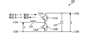
- FIG. 14 is a diagram showing an example of the configuration of a conventional chopper circuit 100 capable of bidirectional operation.
- chopper circuit 100 has a reactor 129 and semiconductor switches 130A and 131A configured with IGBTs (Insulated Gate Bipolar Transistors) or the like.
- Chopper circuit 100 also has diodes (freewheeling diodes) 130D and 131D connected in anti-parallel to semiconductor switches 130A and 131A, respectively, smoothing capacitor 132, circuit terminals 133A and 133B, and circuit terminals 135A and 135B.
- Chopper circuit 100 can operate bidirectionally, i.e., in step-up mode and step-down mode.
- chopper circuit 100 When chopper circuit 100 is in the step-up mode, for example, a DC power supply (not shown) is connected between circuit terminal 133A and circuit terminal 133B, and a load (not shown) is connected between circuit terminal 135A and circuit terminal 135B.
- a load On the other hand, when chopper circuit 100 is in the step-down mode, for example, a load (not shown) is connected between circuit terminal 133A and circuit terminal 133B, and a DC power supply (not shown) is connected between circuit terminal 135A and circuit terminal 135B.
- chopper circuit 100 When chopper circuit 100 is in the step-up mode and step-down mode, current flows in the direction of the arrow shown in FIG. 14.
- semiconductor switch 130A When chopper circuit 100 is in boost mode, semiconductor switch 130A is turned on and off based on a duty ratio determined by the voltage V of a DC power supply (not shown) between circuit terminals 133A and 133B, and the voltage E between circuit terminals 135A and 135B. In other words, semiconductor switch 130A is controlled to be turned on and off so that the voltage E between circuit terminals 135A and 135B is constant. Semiconductor switch 131A is fixed in the off state to operate as a freewheeling diode.
- FIG. 15 is a diagram showing an example of the configuration of another conventional chopper circuit 200 capable of bidirectional operation.
- chopper circuit 200 has reactor 201 and semiconductor switches 202A, 202B, 203A, and 203B composed of IGBTs or the like.
- Chopper circuit 200 also has diodes 202AD, 202BD, 203AD, and 203BD connected in inverse parallel to semiconductor switches 202A, 202B, 203A, and 203B, respectively.
- Chopper circuit 200 also has smoothing capacitors 204A and 204B with a DC voltage of E/2.
- smoothing capacitors 204A and 204B are connected in series.
- a circuit in which semiconductor switches 202A and 203A are connected in series is connected to both ends of smoothing capacitor 204A, and the connection point between semiconductor switches 202A and 203A is connected to terminal 201a of reactor 201.
- a circuit in which semiconductor switches 202B and 203B are connected in series is connected to both ends of smoothing capacitor 204B, and the connection point between semiconductor switches 202B and 203B is connected to terminal 201b of reactor 201.
- Reference numeral 205 indicates a neutral point.
- Circuit terminals 206A and 206B are connected to terminals 201c and 201d of reactor 201, and circuit terminals 207A and 207B are connected to both terminals of smoothing capacitors 204A and 204B connected in series.
- the voltage difference between the power supply voltage V and the capacitor voltage E/2 is applied to the reactor 201 by the semiconductor switch, so the reactor 201 can be made smaller.
- the switching of the semiconductor switch is performed at a voltage of E/2, the loss in the semiconductor switch can be reduced.
- the conduction loss in the semiconductor switch increases because the current always passes through two semiconductor switches.
- semiconductor switches 202A and 202B are alternately switched, and in the step-down mode, semiconductor switches 203A and 203B are alternately switched.
- the potential of power supply V fluctuates (potential swings) with respect to the potential of neutral point 205 of the capacitor voltage (virtual earth potential), which creates the problem of increased noise.
- FIG. 16 is a diagram showing an example of the configuration of a DC power conversion device 210 having the conventional chopper circuit 200 shown in FIG. 15.
- the DC power conversion device 210 has the chopper circuit 200, smoothing capacitors 204A and 204B, a neutral point (virtual earth) 205, a battery 211, floating capacitances 214A and 214B, and an intermediate potential 215 of the battery 211.
- battery 211 such as a storage battery or solar cell
- battery 211 has floating capacitances 214A and 214B between the battery and ground.
- switching of chopper circuit 200 creates a difference between the potential of virtual earth 205 of smoothing capacitors 204A and 204B and intermediate potential 215 of battery 211, causing leakage current to flow through floating capacitances 214A and 214B and the ground.
- the configuration shown in FIG. 16 may cause noise interference.
- battery 211 such as a solar cell
- FIG. 17 is a diagram showing an example of the configuration of a DC power conversion device 300 having another conventional chopper circuit 301 capable of bidirectional operation.
- the DC power conversion device 300 has a chopper circuit 301, four power semiconductor elements 303Q, 304Q, 305Q, and 306Q, a capacitor 313, a capacitor 316, and a reactor 321.
- the source of the power semiconductor element 303Q and the drain of the power semiconductor element 304Q are connected at a connection point 300b.
- the source of the power semiconductor element 305Q and the drain of the power semiconductor element 306Q are connected at a connection point 300c.
- the chopper circuit 301 has a capacitor 323 that functions as a flyback capacitor between the connection points 300b and 300c.
- the chopper circuit 301 shown in FIG. 17 the high-frequency ripple current flowing through the reactor 321 is significantly suppressed at a boost ratio of, for example, about 2, so the reactor 321 can be made smaller.
- the chopper circuit 301 is an effective circuit method for boosting the voltage by about 2 at a current conduction ratio of 50%, for example. That is, as shown in FIG. 17, the chopper circuit 301 is provided with a capacitor 323, and the reactor 321 can be made smaller by configuring the reactor 321 so that the voltage difference between the capacitor 316 and the capacitor 323 is applied to the reactor 321.
- the configuration shown in FIG. 17 requires a dedicated capacitor 323, and there is a problem that the capacitor 323 becomes large.
- the current always passes through two power semiconductor elements (semiconductor switches), which increases the loss of the semiconductor switches.
- the present disclosure therefore aims to provide a DC power conversion device that can reduce the ripple current in the reactor, downsize the reactor, reduce losses in the semiconductor switches, and reduce costs, as well as produce low noise, compared to conventional devices.
- a DC power conversion device includes a chopper circuit having a first switch connected in series between a first connection point and a second connection point, a first diode connected in anti-parallel to the first switch, a second switch connected in series between the first connection point and a third connection point, a second diode connected in anti-parallel to the second switch, a first capacitor connected in series between the second connection point and the third connection point, a second capacitor connected in series between the third connection point and a fourth connection point, and a DC power source and a first reactor connected in series in this order between the fourth connection point and the first connection point, and in a boost mode, when the first switch is in an off state and the second switch is in an on state, a current path is formed in the chopper circuit that passes from the DC power source through the first reactor, the first connection point, the second switch, the third connection point, the second capacitor, and the fourth connection point in this order, and returns to the DC power source.
- a current path is formed from the DC power supply, passing through the first reactor, the first connection point, the first diode, the second connection point, the first capacitor, the third connection point, the second capacitor, and the fourth connection point in this order, and returning to the DC power supply.
- a current path is formed that returns to the second capacitor, passing through the second capacitor, the third connection point, the first capacitor, the second connection point, the first switch, the first connection point, the first reactor, the DC power supply, and the fourth connection point in this order
- a current path is formed that returns to the second capacitor, passing through the second capacitor, the third connection point, the second diode, the first connection point, the first reactor, the DC power supply, and the fourth connection point in this order.
- a DC power conversion device includes a chopper circuit having a first diode connected in series between a first connection point and a second connection point, a second switch connected in series between the first connection point and a third connection point, a second diode connected in anti-parallel to the second switch, a first capacitor connected in series between the second connection point and the third connection point, a second capacitor connected in series between the third connection point and a fourth connection point, and a DC power source and a first reactor connected in series in this order between the fourth connection point and the first connection point.
- the chopper circuit In the boost mode, when the second switch is on, the chopper circuit forms a current path that returns to the DC power supply by passing through the first reactor, the first connection point, the second switch, the third connection point, the second capacitor, and the fourth connection point in that order, and when the second switch is off, forms a current path that returns to the DC power supply by passing through the first reactor, the first connection point, the first diode, the second connection point, the first capacitor, the third connection point, the second capacitor, and the fourth connection point in that order.
- a DC power conversion device includes a chopper circuit having a first switch connected in series between a first connection point and a second connection point, a first diode connected in anti-parallel to the first switch, a second diode connected in series between the first connection point and a third connection point, a first capacitor connected in series between the second connection point and the third connection point, a second capacitor connected in series between the third connection point and a fourth connection point, and a DC power source and a first reactor connected in series in this order between the fourth connection point and the first connection point.
- the chopper circuit forms a current path that returns to the second capacitor by passing through the second capacitor, the third connection point, the first capacitor, the second connection point, the first switch, the first connection point, the first reactor, the DC power supply, and the fourth connection point in that order, and when the first switch is off, forms a current path that returns to the second capacitor by passing through the second capacitor, the third connection point, the second diode, the first connection point, the first reactor, the DC power supply, and the fourth connection point in that order.
- the present disclosure makes it possible to provide a DC power conversion device that can reduce the ripple current in the reactor and the size of the reactor, as well as reduce losses and costs in the semiconductor switches, and is low-noise.
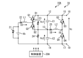
- FIG. 1 is a diagram illustrating an example of a configuration of a DC power conversion device according to a first embodiment.
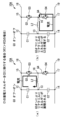
- 2 is a diagram showing a current flow in the chopper circuit shown in FIG. 1 in a boost mode.
- 2 is a diagram showing a current flow in the chopper circuit shown in FIG. 1 in a step-down mode.
- 4 is a diagram showing an example of a configuration of a control device in the DC power conversion device shown in FIGS. 1 to 3 and a control method in a boost mode;
- FIG. 4 is a diagram showing an example of a configuration of a control device in the DC power conversion device shown in FIGS. 1 to 3 and a control method in a step-down mode;
- FIG. 11 is a diagram illustrating an example of the configuration of a DC power conversion device according to a second embodiment.
- 7 is a diagram showing a current flow when energy of a second capacitor is transferred to a first capacitor in the chopper circuit shown in FIG. 6 .
- 7 is a diagram showing a current flow when energy of a first capacitor is transferred to a second capacitor in the chopper circuit shown in FIG. 6 .
- 9 is a diagram showing an example of a configuration of a control device in the DC power conversion device shown in FIGS. 6 to 8 and a control method for controlling the voltage balance between a first capacitor and a second capacitor.
- FIG. FIG. 13 is a diagram illustrating an example of a configuration of a chopper circuit in a DC power conversion device according to a third embodiment.
- FIG. 13 is a diagram showing an example of the configuration of a chopper circuit in a DC power conversion device according to a fourth embodiment.
- FIG. 13 is a diagram illustrating an example of the configuration of a chopper circuit in a DC power conversion device according to a fifth embodiment.
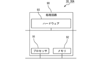
- 13 is a conceptual diagram showing an example of a hardware configuration of a processing circuit included in the control device in the embodiment shown in FIGS. 1 to 12 .
- FIG. FIG. 1 is a diagram showing an example of the configuration of a conventional chopper circuit capable of bidirectional operation.
- FIG. 1 is a diagram showing an example of the configuration of another conventional chopper circuit capable of bidirectional operation.
- FIG. 16 is a diagram showing an example of the configuration of a DC power conversion device having the conventional chopper circuit shown in FIG. 15.
- FIG. 1 is a diagram showing an example of the configuration of a DC power conversion device having another conventional chopper circuit capable of bidirectional operation.
- FIG. 1 is a diagram showing an example of the configuration of a DC power conversion device 1 according to the first embodiment.
- the DC power conversion device 1 has a chopper circuit 10 and a control device 30.
- the DC power conversion device 1 is also called a "DC (Direct Current)/DC converter" and is, for example, a power supply device that creates a DC voltage of a different voltage from a DC power supply that outputs a predetermined voltage.
- Chopper circuit 10 is also called a DC chopper, and for example, changes the DC voltage by repeatedly turning a semiconductor switching element on and off.
- chopper circuit 10 of this embodiment is a buck-boost chopper that can both boost the output DC voltage to a higher voltage than the input DC voltage, and buck the output DC voltage to a lower voltage than the input DC voltage.
- the chopper circuit 10 has a DC power supply Vb, a first reactor L1, a first semiconductor switch Q1, a second semiconductor switch Q2, a first diode D1, a second diode D2, a first capacitor C1, and a second capacitor C2.
- the chopper circuit 10 has these components interconnected via a first connection point 11, a second connection point 12, a third connection point 13, and a fourth connection point 14.
- first capacitor C1 and the second capacitor C2 are connected in series via the third connection point 13 and the first semiconductor switch Q1 and the second semiconductor switch Q2 are connected in series via the first connection point 11.
- the first semiconductor switch Q1 and the second semiconductor switch Q2 connected in series are connected to both ends of the first capacitor C1 via the second connection point 12 and the third connection point 13 at both ends of the first capacitor C1.
- the first connection point 11, which is the connection point between the first semiconductor switch Q1 and the second semiconductor switch Q2 is connected to one end of the first reactor L1, and the other end of the first reactor L1 is connected to one end of the DC power source Vb.
- the other end of the DC power source Vb is connected to the second capacitor C2 via the fourth connection point 14.
- the first diode D1 is connected in anti-parallel to the first semiconductor switch Q1, and the second diode D2 is connected in anti-parallel to the second semiconductor switch Q2.
- the DC power supply Vb is, for example, a storage battery, and is connected in series between the fourth connection point 14 and the first reactor L1.
- the DC power supply Vb discharges power toward the first capacitor C1 and the second capacitor C2.
- the DC power supply Vb is charged by the power received from the first capacitor C1 and the second capacitor C2.
- the first reactor L1 is connected in series between the DC power source Vb and the first connection point 11. For example, when the chopper circuit 10 (DC power conversion device 1) is in boost mode, the first reactor L1 stores energy from the power supplied from the DC power source Vb, and boosts the first capacitor C1 and the second capacitor C2 with the stored energy.
- the first semiconductor switch Q1 is connected between the first connection point 11 and the second connection point 12, and the second semiconductor switch Q2 is connected between the first connection point 11 and the third connection point 13.
- the first semiconductor switch Q1 and the second semiconductor switch Q2 are semiconductor switching elements formed of, for example, IGBTs.
- the first semiconductor switch Q1 and the second semiconductor switch Q2 perform switching based on, for example, a chopper duty according to the output voltage, output current, etc.
- the on/off operation of the first semiconductor switch Q1 and the second semiconductor switch Q2 is controlled by, for example, a gate drive signal (gate signal) output from the control device 30.
- the chopper duty is, for example, the on/off time ratio of the semiconductor switching element, and is also called the "on duty" or "duty ratio".
- the first semiconductor switch Q1 is an example of a "first switch”
- the second semiconductor switch Q2 is an example of a "second switch”.
- the first diode D1 is connected in anti-parallel to the first semiconductor switch Q1, and the second diode D2 is connected in anti-parallel to the second semiconductor switch Q2.
- the first diode D1 and the second diode D2 are, for example, return diodes that return energy to the DC power supply Vb when the IGBT is turned off.
- the first capacitor C1 is connected in series between the second connection point 12 and the third connection point 13, and the second capacitor is connected in series between the third connection point 13 and the fourth connection point 14.
- the first capacitor C1 and the second capacitor C2 are DC smoothing capacitors that smooth out voltage fluctuations (ripples).
- the first capacitor C1 and the second capacitor C2 are charged by power received from the DC power source Vb.
- the first capacitor C1 and the second capacitor C2 discharge power toward the DC power source Vb.
- a first voltage sensor 21, a first current sensor 22, a second voltage sensor 23, and a third voltage sensor 24 are arranged in the DC power conversion device 1.
- the positions at which the first voltage sensor 21, the first current sensor 22, the second voltage sensor 23, and the third voltage sensor 24 are arranged are not limited to the positions shown in FIG. 1, and these sensors may be arranged anywhere as long as they can acquire the current or voltage values they are intended to acquire. Note that in FIG. 2 and subsequent figures, the illustration of these sensors is omitted as appropriate.
- the first voltage sensor 21 is disposed, for example, at a position where it can detect the voltage across the DC power supply Vb, and constantly detects the value of the voltage VVb of the DC power supply Vb.
- the value of the voltage VVb of the DC power supply Vb detected by the first voltage sensor 21 is acquired (monitored) by the control device 30.
- the first current sensor 22 is disposed, for example, at a position where it can detect the current flowing through the first reactor L1, and constantly detects the value of the current ID flowing through the first reactor L1.
- the value of the current ID flowing through the first reactor L1 detected by the first current sensor 22 is acquired (monitored) by the control device 30.
- the second voltage sensor 23 is disposed, for example, at a position where it can detect the voltage of the first capacitor C1, and constantly detects the value of the voltage VC1 of the first capacitor C1.
- the value of the voltage VC1 of the first capacitor C1 detected by the second voltage sensor 23 is acquired (monitored) by the control device 30.
- the third voltage sensor 24 is disposed, for example, at a position where it can detect the voltage of the second capacitor C2, and constantly detects the value of the voltage VC2 of the second capacitor C2.
- the value of the voltage VC2 of the second capacitor C2 detected by the third voltage sensor 24 is acquired (monitored) by the control device 30.
- the control device 30 has a processor 91 (see FIG. 13), such as a CPU (Central Processing Unit) that operates by executing a program.
- the control device 30 has a memory 92 (see FIG. 13), and generally controls the operation of the DC power conversion device 1 (chopper circuit 10) by operating the processor 91, for example, by executing a predetermined program stored in the memory 92.
- the control device 30 may operate according to instructions received from an operator, for example, via a higher-level device (not shown) or an operation unit (not shown).
- the control device 30 is connected to each part of the DC power conversion device 1 via signal lines (not shown).
- the control device 30 controls the operation of the first semiconductor switch Q1 and the second semiconductor switch Q2, for example, based on current and voltage values acquired from the first voltage sensor 21, the first current sensor 22, the second voltage sensor 23, and the third voltage sensor 24.
- the detailed configuration and control method (operation) of the control device 30 will be described later (see Figures 4 and 5, etc.).
- FIG. 2 is a diagram showing the current flow in the chopper circuit 10 shown in FIG. 1 in the boost mode.
- FIG. 2(a) is a diagram showing the current flow in the chopper circuit 10 shown in FIG. 1 when the second semiconductor switch Q2 is in the on state in the boost mode.
- FIG. 2(b) is a diagram showing the current flow in the chopper circuit 10 shown in FIG. 1 when the second semiconductor switch Q2 is in the off state in the boost mode.
- FIG. 3 is a diagram showing the current flow in the chopper circuit 10 shown in FIG. 1 in the step-down mode.
- FIG. 3(a) is a diagram showing the current flow in the chopper circuit 10 shown in FIG. 1 when the first semiconductor switch Q1 is in the on state in the step-down mode.
- FIG. 3(b) is a diagram showing the current flow in the chopper circuit 10 shown in FIG. 1 when the first semiconductor switch Q1 is in the off state in the step-down mode.
- the following current path is formed in the chopper circuit 10. That is, a current path is formed that passes through the second capacitor C2, the third connection point 13, the first capacitor C1, the second connection point 12, the first semiconductor switch Q1, the first connection point 11, the first reactor L1, the DC power supply Vb, and the fourth connection point 14 in this order, and returns to the second capacitor C2.
- FIG. 4 is a diagram showing an example of the configuration of the control device 30 in the DC power conversion device 1 shown in FIGS. 1 to 3 and a control method in the boost mode.
- the control device 30 has a memory 92 (see FIG. 13) described below, and functions as the following components by, for example, executing a predetermined program stored in the memory 92 described below. That is, the control device 30 functions as a first subtractor 31, a voltage controller 32, a second subtractor 33, a current controller 34, and a PWM (Pulse Width Modulation) control unit 35 by executing a predetermined program.
- Each of the above functions may be realized by a program executed by a processor 91 (see FIG. 13) possessed by the control device 30, or by hardware 93 (see FIG. 13). In the boost mode, each of the above components executes a predetermined program to perform the following processes.
- the first subtractor 31 obtains the VC reference, for example, from the memory 92 (see FIG. 13) described below.
- the VC reference is a predetermined voltage reference value (voltage command value) for controlling the value of the voltage VC, which is the sum of the voltage VC1 of the first capacitor C1 and the voltage VC2 of the second capacitor C2, to a predetermined value or a constant value.
- the first subtractor 31 may calculate the VC reference based on a predetermined calculation, for example, or may obtain the VC reference by receiving instructions from a higher-level device (not shown) or an operator (not shown).
- the first subtractor 31 also obtains (feeds back) the value of the voltage VC1 of the first capacitor C1 from the second voltage sensor 23 (see FIG. 1), and obtains (feeds back) the value of the voltage VC2 of the second capacitor C2 from the third voltage sensor 24 (see FIG. 1).
- the first subtractor 31 obtains (feeds back) the value of the voltage VC, which is the value of the voltage VC1 of the first capacitor C1 plus the value of the voltage VC2 of the second capacitor C2, from the second voltage sensor 23 and the third voltage sensor 24.
- the first subtractor 31 subtracts the obtained value of the voltage VC (or the value of voltage VC1+VC2) from the obtained (or calculated) VC reference, and outputs the subtracted value to the voltage controller 32.
- the voltage controller 32 performs, for example, PI (Proportional-Integral) control on the value acquired from the first subtractor 31 to obtain an ID reference.
- the ID reference is a reference value (current command value) of the current to be passed through the first reactor L1 in order to control the value of the voltage VC, which is the sum of the voltage VC1 of the first capacitor C1 and the voltage VC2 of the second capacitor C2, to a predetermined value or a constant value.
- the voltage controller 32 outputs the obtained ID reference to the second subtractor 33.
- the first subtractor 31 and the voltage controller 32 are examples of a "voltage control unit", the VC reference is an example of a "first voltage command value”, and the ID reference is an example of a "first current command value”.
- the second subtractor 33 obtains the ID reference from the voltage controller 32.
- the second subtractor 33 also obtains (feeds back) the value of the current ID flowing through the first reactor L1 from the first current sensor 22 (see FIG. 1).
- the second subtractor 33 then subtracts the obtained value of the current ID from the obtained ID reference, and outputs the subtracted value to the current controller 34.
- the current controller 34 performs, for example, PI control on the value acquired from the second subtractor 33 to obtain a voltage command value V1 * which is a duty command (chopper duty) in the boost mode.
- the current controller 34 outputs the obtained voltage command value V1 * to the PWM control unit 35.
- the second subtractor 33 and the current controller 34 are an example of a "current control unit", and the voltage command value V1 * is an example of a "second voltage command value”.
- the PWM control unit 35 performs PWM control based on the voltage command value V1 * obtained from the current controller 34 and, for example, a carrier signal having a predetermined triangular waveform, and generates a gate signal, which is a pulse width modulation (PWM) signal for controlling the operation of the second semiconductor switch Q2.
- the PWM control unit 35 outputs the generated gate signal (Q2 pulse) to the second semiconductor switch Q2 to control the on/off operation of the second semiconductor switch Q2.
- the Q2 pulse is an example of a "first pulse.”
- the on/off operation of the second semiconductor switch Q2 can be controlled using the above control method to charge the first capacitor C1 and the second capacitor C2 from the DC power source Vb, thereby boosting the voltage.
- FIG. 5 shows an example of the configuration of the control device 30 in the DC power conversion device 1 shown in FIGS. 1 to 3 and a control method in the step-down mode.
- control device 30 executes a predetermined program to function as a first subtractor 31, a voltage controller 32, a second subtractor 33, a current controller 34, and a PWM control unit 35.
- a predetermined program to function as a first subtractor 31, a voltage controller 32, a second subtractor 33, a current controller 34, and a PWM control unit 35.
- each of the above units executes a predetermined program to perform the following processes.
- the first subtractor 31 obtains the Vb reference, for example, from the memory 92 (see FIG. 13) described below.
- the Vb reference is a predetermined voltage reference value (voltage command value) for controlling the value of the voltage VVb of the DC power supply Vb to a predetermined value or a constant value.
- the Vb reference is a voltage reference value (voltage command value) for how many volts the value of the voltage VVb of the DC power supply (battery) Vb should be, for example, 500 volts.
- the first subtractor 31 may calculate the Vb reference based on a predetermined calculation, for example, or may obtain the Vb reference by receiving instructions from a higher-level device (not shown) or an operator (not shown).
- the first subtractor 31 also acquires (feeds back) the value of the voltage VVb of the DC power supply Vb from the first voltage sensor 21 (see FIG. 1). The first subtractor 31 then subtracts the acquired value of the voltage VVb from the acquired (or calculated) Vb reference, and outputs the subtracted value to the voltage controller 32.
- the voltage controller 32 performs, for example, PI control on the value obtained from the first subtractor 31 to obtain an ID reference.
- the ID reference here is a reference value (current command value) of the current to be passed through the first reactor L1 in order to control the value of the voltage VVb of the DC power supply Vb to a predetermined value or a constant value.
- the voltage controller 32 outputs the obtained ID reference to the second subtractor 33.
- the Vb reference is an example of a "third voltage command value”
- the ID reference here is an example of a "second current command value.”
- the second subtractor 33 obtains the ID reference from the voltage controller 32.
- the second subtractor 33 also obtains (feeds back) a value obtained by multiplying the value of the current ID flowing through the first reactor L1 from the first current sensor 22 (see FIG. 1) by -1.
- the reason why the value of the current ID is multiplied by -1 is because in the step-down mode, the current direction is the opposite polarity to that in the step-up mode. In other words, since the current direction is opposite between the charging direction and the discharging direction, the value of the current ID is multiplied by -1 to make the control consistent.
- the second subtractor 33 then subtracts the value obtained by multiplying the obtained value of the current ID by -1 from the obtained ID reference, and outputs the subtracted value to the current controller 34.
- the current controller 34 performs, for example, PI control on the value acquired from the second subtractor 33 to obtain a voltage command value V2 * which is a duty command (chopper duty) in the step-down mode.
- the current controller 34 outputs the obtained voltage command value V2 * to the PWM control unit 35.
- the voltage command value V2 * is an example of a "fourth voltage command value.”
- the PWM control unit 35 performs PWM control based on the voltage command value V2 * obtained from the current controller 34 and, for example, a carrier signal having a predetermined triangular waveform, and generates a gate signal, which is a pulse width modulation (PWM) signal for controlling the operation of the first semiconductor switch Q1.
- the PWM control unit 35 outputs the generated gate signal (Q1 pulse) to the first semiconductor switch Q1 to control the on/off operation of the first semiconductor switch Q1.
- the Q1 pulse is an example of a "second pulse.”
- the DC power source Vb can be charged from the first capacitor C1 and the second capacitor C2 and stepped down by controlling the on/off operation of the first semiconductor switch Q1 using the above control method.
- the voltage applied to the first reactor L1 is the difference between the voltage VVb of the DC power supply Vb and the voltage VC2 of the second capacitor C2, so that it is possible to reduce the ripple current of the first reactor L1.
- This makes it possible to reduce the loss and size of the first reactor L1. That is, according to the first embodiment shown in Figures 1 to 5, it is possible to reduce the ripple current of the first reactor L1 and to reduce the size of the first reactor L1 compared to the conventional art.
- a current path is formed that passes through only one of the first semiconductor switch Q1 and the second semiconductor switch Q2. Furthermore, the first semiconductor switch Q1 and the second semiconductor switch Q2 switch switching within the voltage range of the voltage VC1 of the first capacitor C1. Therefore, it is possible to reduce the switching loss of the first semiconductor switch Q1 and the second semiconductor switch Q2. As a result, it is possible to apply inexpensive semiconductor switches with low rated voltages to the first semiconductor switch Q1 and the second semiconductor switch Q2. In other words, according to the first embodiment shown in FIG. 1 to FIG. 5, it is possible to reduce the loss and the cost of the first semiconductor switch Q1 and the second semiconductor switch Q2 compared to the conventional art.
- the negative electrode of the capacitor and the negative electrode of the DC power source Vb are connected. Therefore, the negative electrode of the DC power conversion device 1 (chopper circuit 10) and the negative electrode of the DC power source Vb are common, so the potential difference is small and the leakage current is small. As a result, the potential between the ground is fixed, and noise interference due to leakage current (see Fig. 16) is reduced, resulting in low noise.
- Second Embodiment Fig. 6 is a diagram showing an example of the configuration of a DC power conversion device 1A according to the second embodiment.
- the same or similar configurations as those of the first embodiment shown in Figs. 1 to 5 are denoted by the same reference numerals, and duplicated or detailed descriptions are omitted or simplified.
- a configuration for uniformly controlling the voltage balance between the first capacitor C1 and the second capacitor C2 is added to the DC power conversion device 1 shown in Figs. 1 to 5.
- the DC power conversion device 1A has a chopper circuit 10A and a control device 30A.
- the DC power conversion device 1A (chopper circuit 10A) has the following configuration in addition to the configuration of the DC power conversion device 1 (chopper circuit 10) shown in FIG. 1. That is, the DC power conversion device 1A (chopper circuit 10A) has a third semiconductor switch Q3, a fourth semiconductor switch Q4, a third diode D3, a fourth diode D4, and a second reactor L2 in addition to the configuration shown in FIG. 1. In the chopper circuit 10A, these components are connected to each other via the second connection point 12, the third connection point 13, the fourth connection point 14, the fifth connection point 15, the sixth connection point 16, and the seventh connection point 17.
- two sets of semiconductor switches are added by connecting a third semiconductor switch Q3 and a fourth semiconductor switch Q4 to both ends of the first capacitor C1 and the second capacitor C2.
- a second reactor L2 is connected between a sixth connection point 16, which is the connection point between the third semiconductor switch Q3 and the fourth semiconductor switch Q4, and a third connection point 13, which is the connection point between the first capacitor C1 and the second capacitor C2.
- the third diode D3 is connected in anti-parallel to the third semiconductor switch Q3, and the fourth diode D4 is connected in anti-parallel to the fourth semiconductor switch Q4.
- the fifth connection point is connected to the first terminal 18 on the right side in FIG. 6, and the seventh connection point is connected to the second terminal 19 on the right side in FIG. 6.
- a load (not shown) is connected between the first terminal 18 and the second terminal 19.
- the third semiconductor switch Q3 is connected in series between the fifth connection point 15 between the second connection point 12 and the first terminal 18 and the sixth connection point 16, and the fourth semiconductor switch Q4 is connected in series between the sixth connection point 16 and the seventh connection point 17 between the fourth connection point 14 and the second terminal 19.
- the third semiconductor switch Q3 and the fourth semiconductor switch Q4 are semiconductor switching elements composed of, for example, IGBTs.
- the third semiconductor switch Q3 and the fourth semiconductor switch Q4 perform switching based on, for example, the voltage difference between the voltage VC1 of the first capacitor C1 and the voltage VC2 of the second capacitor C2.
- the on/off operation of the third semiconductor switch Q3 and the fourth semiconductor switch Q4 is controlled by, for example, a gate drive signal (gate signal) output from the control device 30A.
- the third semiconductor switch Q3 is an example of a "third switch”
- the fourth semiconductor switch Q4 is an example of a "fourth switch”.
- the third diode D3 is connected in anti-parallel to the third semiconductor switch Q3, and the fourth diode D4 is connected in anti-parallel to the fourth semiconductor switch Q4.
- the third diode D3 and the fourth diode D4 are, for example, return diodes that return energy to the first capacitor C1 side or the second capacitor C2 side when the IGBT is turned off.
- the second reactor L2 is connected in series between the third connection point 13 and the sixth connection point 16. As described below (see Figures 7, 8, etc.), the second reactor L2 functions as a balancer for controlling the voltage balance between the voltage VC1 of the first capacitor C1 and the voltage VC2 of the second capacitor C2 to a constant or arbitrary value.
- the charge/discharge energies of the first capacitor C1 and the second capacitor C2 are different, so a voltage difference may occur between the voltage VC1 of the first capacitor C1 and the voltage VC2 of the second capacitor C2.
- the voltage of the second capacitor C2 may become higher than the voltage of the first capacitor C1.
- a voltage difference may occur between the voltage VC1 of the first capacitor C1 and the voltage VC2 of the second capacitor C2.
- the second reactor L2 is connected in series between the sixth connection point 16 and the third connection point 13. This allows the voltage balance between the voltage VC1 of the first capacitor C1 and the voltage VC2 of the second capacitor C2 to be arbitrarily controlled by switching the third semiconductor switch Q3 and the fourth semiconductor switch Q4.
- a second current sensor 25 is disposed in the DC power conversion device 1A.
- the position at which the second current sensor 25 is disposed is not limited to the position shown in FIG. 6, and the sensor may be disposed anywhere as long as it is capable of obtaining the value of the current that it is intended to obtain. Note that in FIG. 7 and subsequent figures, the illustration of the second current sensor 25 is omitted as appropriate.
- the second current sensor 25 is disposed, for example, at a position where it can detect the current flowing through the second reactor L2, and constantly detects the value of the current IB flowing through the second reactor L2.
- the value of the current IB flowing through the second reactor L2 detected by the second current sensor 25 is acquired (monitored) by the control device 30A.
- the control device 30A is connected to each part of the DC power conversion device 1A via signal lines (not shown) and has the same functions as the control device 30 in the first embodiment shown in Figs. 1 to 5. That is, the control device 30A controls the operation of the first semiconductor switch Q1 and the second semiconductor switch Q2 based on the current and voltage values obtained from each sensor. The control device 30A also controls the operation of the third semiconductor switch Q3 and the fourth semiconductor switch Q4 based on the current and voltage values obtained from each sensor. The detailed configuration and control method (operation) of the control device 30A will be described later (see Fig. 9, etc.).
- FIG. 7 is a diagram showing the current flow when the energy of the second capacitor C2 is transferred to the first capacitor C1 in the chopper circuit 10A shown in FIG. 6.
- FIG. 7(a) is a diagram showing the current flow when the fourth semiconductor switch Q4 is in the on state in the case where the energy stored in the second capacitor C2 is greater than the energy stored in the first capacitor C1.
- FIG. 7(b) is a diagram showing the current flow when the fourth semiconductor switch Q4 is in the off state in the case where the energy stored in the second capacitor C2 is greater than the energy stored in the first capacitor C1.
- the following current path is formed. That is, a current path is formed that passes through the second reactor L2, the sixth connection point 16, the third diode D3, the fifth connection point 15, the second connection point 12, the first capacitor C1, and the third connection point 13 in this order, and returns to the second reactor L2.
- the energy stored in the second reactor L2 is stored in the first capacitor C1, and the first capacitor C1 is charged.
- the voltage VC1 of the first capacitor C1 and the voltage VC2 of the second capacitor C2 are balanced (uniform).
- FIG. 8 is a diagram showing the current flow when the energy of the first capacitor C1 is transferred to the second capacitor C2 in the chopper circuit 10A shown in FIG. 6.
- FIG. 8(a) is a diagram showing the current flow when the third semiconductor switch Q3 is in the on state in the case where the energy stored in the first capacitor C1 is greater than the energy stored in the second capacitor C2.
- FIG. 8(b) is a diagram showing the current flow when the third semiconductor switch Q3 is in the off state in the case where the energy stored in the first capacitor C1 is greater than the energy stored in the second capacitor C2.
- the following current path is formed when the third semiconductor switch Q3 is turned on and the fourth semiconductor switch Q4 is turned off. That is, a current path is formed that passes through the first capacitor C1, the second connection point 12, the fifth connection point 15, the third semiconductor switch Q3, the sixth connection point 16, the second reactor L2, and the third connection point 13 in this order, and returns to the first capacitor C1.
- the energy stored in the first capacitor C1 is stored in the second reactor L2.
- the following current path is formed. That is, a current path is formed that passes through the second reactor L2, the third connection point 13, the second capacitor C2, the fourth connection point 14, the seventh connection point 17, the fourth diode D4, and the sixth connection point 16 in this order, and returns to the second reactor L2.
- the energy stored in the second reactor L2 is stored in the second capacitor C2, and the second capacitor C2 is charged.
- the voltage VC1 of the first capacitor C1 and the voltage VC2 of the second capacitor C2 are balanced (uniform).
- the chopper circuit 10A includes a circuit having the third semiconductor switch Q3, the fourth semiconductor switch Q4, and the second reactor L2, no current flows through these. In other words, in the chopper circuit 10A, when the chopper duty is 100%, the current passes through only one semiconductor switch, and does not necessarily pass through two semiconductor switches.
- FIG. 9 is a diagram showing an example of the configuration of the control device 30A in the DC power conversion device 1A shown in FIGS. 6 to 8 and a control method for controlling the voltage balance between the first capacitor C1 and the second capacitor C2.
- control device 30A has the same functions as the control device 30 in the first embodiment shown in Figures 1 to 5. Therefore, the control device 30A controls the operation of the first semiconductor switch Q1 and the second semiconductor switch Q2 by the control method described in Figures 4 and 5. Furthermore, the control device 30A controls the operation of the third semiconductor switch Q3 and the fourth semiconductor switch Q4 as follows.
- the control device 30A controls the operation of the third semiconductor switch Q3 and the fourth semiconductor switch Q4 so that both the third semiconductor switch Q3 and the fourth semiconductor switch Q4 are in the off state when the chopper duty of the chopper circuit 10A is 100%.
- the chopper duty is 100%, equal energy flows through the first capacitor C1 and the second capacitor C2, so the voltage VC1 of the first capacitor C1 and the voltage VC2 of the second capacitor C2 are balanced (uniform).
- control device 30A executes a predetermined program to function as a first subtractor 31A, a voltage controller 32A, a second subtractor 33A, a current controller 34A, and a PWM control unit 35A.
- Each of the above units executes a predetermined program to perform the following processes.
- the first subtractor 31A performs the same processing as the first subtractor 31 in the first embodiment shown in FIG. 1 to FIG. 5. Furthermore, the first subtractor 31A acquires the VC2 reference from, for example, a memory 92 (see FIG. 13) described later.
- the VC2 reference is a predetermined voltage reference value (voltage command value) for controlling the value of the voltage VC2 of the second capacitor C2 to be equal to the value of the voltage VC1 of the first capacitor C1.
- the VC2 reference is also a predetermined voltage reference value (voltage command value) for controlling the value of the voltage VC2 of the second capacitor C2 to be equal to or lower than the value of the voltage VVb of the DC power supply Vb.
- the first subtractor 31A may calculate the VC2 reference based on a predetermined calculation or the like, or may acquire the VC2 reference by receiving an instruction from a higher-level device (not shown) or an operator (not shown).
- the first subtractor 31A also acquires (feeds back) the value of the voltage VC2 of the second capacitor C2 from the third voltage sensor 24 (see FIG. 6). The first subtractor 31A then subtracts the acquired (or calculated) VC2 reference from the acquired value of the voltage VC2, and outputs the subtracted value to the voltage controller 32A.
- the voltage controller 32A performs the same processing as the voltage controller 32 in the first embodiment shown in Figs. 1 to 5. Furthermore, the voltage controller 32A performs, for example, PI control on the value acquired from the first subtractor 31A to obtain the IB reference.
- the IB reference is a reference value (current command value) of the current to be passed through the second reactor L2 in order to control the value of the voltage VC2 of the second capacitor C2 to be equal to the value of the voltage VC1 of the first capacitor C1.
- the voltage controller 32A outputs the obtained IB reference to the second subtractor 33A.
- the first subtractor 31A and the voltage controller 32A are examples of a "voltage control unit"
- the VC2 reference is an example of a "fifth voltage command value”
- the IB reference is an example of a "third current command value”.
- the second subtractor 33A performs the same processing as the second subtractor 33 in the first embodiment shown in Figures 1 to 5. Furthermore, the second subtractor 33A obtains the IB reference from the voltage controller 32A. The second subtractor 33A also obtains (feeds back) the value of the current IB flowing through the second reactor L2 from the second current sensor 25 (see Figure 6). The second subtractor 33A then subtracts the obtained value of the current IB from the obtained IB reference, and outputs the subtracted value to the current controller 34A.
- the current controller 34A performs the same processing as the current controller 34 in the first embodiment shown in Fig. 1 to Fig. 5. Furthermore, the current controller 34A performs, for example, PI control or the like on the value acquired from the second subtractor 33A to obtain a voltage command value V3 * which is a command for controlling the value of the voltage VC2 of the second capacitor C2 to be uniform with the value of the voltage VC1 of the first capacitor C1. The current controller 34A outputs the obtained voltage command value V3 * to the PWM control unit 35A.
- the second subtractor 33A and the current controller 34A are an example of a "current control unit", and the voltage command value V3 * is an example of a "sixth voltage command value".
- the PWM control unit 35A performs the same process as the PWM control unit 35 in the first embodiment shown in FIG. 1 to FIG. 5. Furthermore, the PWM control unit 35A performs PWM control based on the voltage command value V3 * acquired from the current controller 34A and, for example, a carrier signal having a predetermined triangular waveform.
- the PWM control unit 35A generates a gate signal, which is a pulse width modulation (PWM) signal for controlling the operation of at least one of the third semiconductor switch Q3 and the fourth semiconductor switch Q4.
- PWM control unit 35A outputs the generated gate signal (Q3, Q4 pulse) to at least one of the third semiconductor switch Q3 and the fourth semiconductor switch Q4.
- the PWM control unit 35A controls the on/off operation of at least one of the third semiconductor switch Q3 and the fourth semiconductor switch Q4.
- the Q3 and Q4 pulses are an example of a "third pulse".
- the PWM control unit 35A controls the operation of the third semiconductor switch Q3 and the fourth semiconductor switch Q4 so that both the third semiconductor switch Q3 and the fourth semiconductor switch Q4 are in the off state when the chopper duty of the chopper circuit 10A is 100%.
- the on/off operation of at least one of the third semiconductor switch Q3 and the fourth semiconductor switch Q4 is controlled by the above control method. This makes it possible to control the voltage VC1 of the first capacitor C1 and the voltage VC2 of the second capacitor C2 to be uniform or in any desired balance.
- control device 30A may also control the voltage VC1 of the first capacitor C1 so that it is equal to the voltage VC2 of the second capacitor C2.
- the first subtractor 31A acquires (calculates) the VC1 reference, and acquires (feeds back) the value of the voltage VC1 of the first capacitor C1.
- the first subtractor 31A then subtracts the acquired (calculated) VC1 reference from the acquired value of the voltage VC1, and outputs the subtracted value to the voltage controller 32A.
- the gate signal (Q3, Q4 pulse) generated and output by the PWM control unit 35A has a pulse opposite to the gate signal (Q3, Q4 pulse) generated and output in the above description.
- the control device 30A can control the voltage VC1 of the first capacitor C1 and the voltage VC2 of the second capacitor C2 to be uniform or arbitrarily balanced, as in the above control method.
- the charging energy of the second capacitor C2 can be transferred to the first capacitor C1 via the second reactor L2.
- the charging energy of the first capacitor C1 can be transferred to the second capacitor C2 via the second reactor L2.
- the voltage VC2 of the second capacitor C2 can be optimized to reduce the ripple current of the first reactor L1.
- the voltage VC1 of the first capacitor C1 and the voltage VC2 of the second capacitor C2 are balanced (uniform). This eliminates the need for switching the third semiconductor switch Q3 and the fourth semiconductor switch Q4, so in this case, no current flows through the third semiconductor switch Q3 and the fourth semiconductor switch Q4. In this case, since the current passes through only one semiconductor switch (it does not necessarily pass through two semiconductor switches), the total loss of the semiconductor switches is reduced and efficiency can be improved compared to the conventional method in which the current always passes through two semiconductor switches.
- FIG. 10 is a diagram showing an example of the configuration of a chopper circuit 10B in a DC power conversion device 1B according to the third embodiment.
- the same or similar components as those in the first and second embodiments shown in Figures 1 to 9 are given the same reference numerals, and duplicated or detailed descriptions are omitted or simplified.
- the first semiconductor switch Q1 in the chopper circuit 10 of the first embodiment shown in Figures 1 to 5 is omitted, and only the first diode D1 is connected in that position.
- the other components and the concept of the control method are the same as those in the boost mode of the first embodiment shown in Figures 1 to 5.
- the DC power conversion device 1B (chopper circuit 10B) according to the third embodiment, only the boost mode is performed. That is, for example, if the DC power conversion device 1 (chopper circuit 10) is one that performs only the boost mode, the first semiconductor switch Q1 can be omitted, and the corresponding position can be configured with only the first diode D1. With this third embodiment shown in FIG. 10, it is possible to achieve the same effect as the boost mode of the first embodiment shown in FIGS. 1 to 5.
- the DC power conversion device 1A (chopper circuit 10A) of the second embodiment shown in Figures 6 to 9 only operates in the boost mode, the first semiconductor switch Q1 can be omitted and the corresponding part can be configured with only the first diode D1. Even with such a configuration, it is possible to achieve the same effect as the boost mode of the second embodiment shown in Figures 6 to 9.
- FIG. 11 is a diagram showing an example of the configuration of a chopper circuit 10C in a DC power conversion device 1C according to the fourth embodiment.
- the same or similar components as those in the first and second embodiments shown in Figures 1 to 9 are given the same reference numerals, and duplicated or detailed descriptions are omitted or simplified.
- the second semiconductor switch Q2 in the chopper circuit 10 of the first embodiment shown in Figures 1 to 5 is omitted, and only the second diode D2 is connected in that position.
- the other components and the concept of the control method are the same as those in the step-down mode of the first embodiment shown in Figures 1 to 5.
- the DC power conversion device 1C (chopper circuit 10C) according to the fourth embodiment, only the step-down mode is performed. That is, for example, if the DC power conversion device 1 (chopper circuit 10) is one that only performs the step-down mode, the second semiconductor switch Q2 can be omitted, and the corresponding position can be configured with only the second diode D2. With such a fourth embodiment shown in FIG. 11, it is possible to achieve the same effect as the step-down mode of the first embodiment shown in FIGS. 1 to 5.
- the second semiconductor switch Q2 can be omitted and the corresponding part can be configured with only the second diode D2. Even with such a configuration, it is possible to achieve the same effect as the step-down mode of the second embodiment shown in Figures 6 to 9.
- FIG. 12 is a diagram showing an example of the configuration of a chopper circuit 10D in a DC power conversion device 1D according to the fifth embodiment.
- the chopper circuit 10D in the DC power conversion device 1D according to the fifth embodiment has a configuration in which the positive and negative sides of the chopper circuit 10A in the DC power conversion device 1A according to the second embodiment shown in FIGS. 6 to 9 are swapped.
- the other components and the concept of the control method are the same as those in the second embodiment shown in FIGS. 6 to 9.
- the chopper circuit 10 in the DC power conversion device 1 according to the first embodiment shown in FIGS. 1 to 5 may also have a configuration in which the positive and negative sides are interchanged. That is, in the chopper circuit 10 according to the first embodiment shown in FIGS. 1 to 5, the negative side of the DC power source Vb is connected to the second capacitor C2, but the positive side of the DC power source Vb may be connected to the first capacitor C1. With such a configuration, it is possible to achieve the same effects as those of the first embodiment shown in FIGS. 1 to 5.
- the third embodiment shown in FIG. 10 and the fourth embodiment shown in FIG. 11 can also be configured similarly to the fifth embodiment shown in FIG. 12, and in this case too, the same effects as those of the third embodiment shown in FIG. 10 and the fourth embodiment shown in FIG. 11 can be achieved.
- Fig. 13 is a conceptual diagram showing an example of a hardware configuration of the processing circuitry 90 included in the control device 30, 30A in the embodiment shown in Figs. 1 to 12.
- the processing circuitry 90 includes at least one processor 91 and at least one memory 92.
- the processing circuitry 90 includes at least one dedicated hardware 93.
- each function is realized by software, firmware, or a combination of software and firmware. At least one of the software and firmware is written as a program. At least one of the software and firmware is stored in the memory 92.
- the processor 91 realizes each function by reading and executing the program stored in the memory 92.
- the processing circuitry 90 may be, for example, a single circuit, a composite circuit, a programmed processor, or a combination of these. Each function is realized by the processing circuitry 90.
- the third semiconductor switch Q3 can be configured with only the third diode D3.
- the fourth semiconductor switch Q4 can be configured with only the fourth diode D4.
- the DC power conversion devices 1 to 1D and the control devices 30 and 30A that they have have been described as an example of one aspect of the present disclosure, but the present disclosure can also be realized as a control method in which processing steps are performed in each part of the control devices 30 and 30A.
- the present disclosure can also be realized as a control program that causes a computer to execute the processing steps in each part of the control device 30, 30A.
- the present disclosure can also be realized as a storage medium (non-transitory computer-readable storage medium) on which a control program is stored.
- the control program can be stored and distributed on removable media such as a CD (Compact Disc), a DVD (Digital Versatile Disc), or a USB (Universal Serial Bus) memory.
- the control program may be uploaded onto a network via a network interface (not shown) possessed by the control device 30, 30A, or may be downloaded from the network and stored in memory 92, etc.
- first subtractor 32, 32A ...Voltage controller; 33, 33A...Second subtractor; 34, 34A...Current controller; 35, 35A...PWM control unit; 90...Processing circuit; 91...Processor; 92...Memory; 93...Hardware; 100...Chopper circuit; 129...Reactor; 130A, 131A...Semiconductor switch; 130D, 131D...Diode; 132...Smoothing capacitor; 133A, 133B, 135A, 135B...Circuit terminal; 200...Chopper circuit; 201...Reactor; 201a, 201b, 201c...Terminal; 20 2A, 202B, 203A, 203B...semiconductor switches; 202AD, 202BD, 203AD, 203BD...diodes; 204A, 204B...smoothing capacitors; 205...neutral point (virtual earth); 206A, 207A...
Landscapes
- Engineering & Computer Science (AREA)
- Power Engineering (AREA)
- Dc-Dc Converters (AREA)
Priority Applications (4)
| Application Number | Priority Date | Filing Date | Title |
|---|---|---|---|
| JP2024547623A JP7764972B2 (ja) | 2023-01-16 | 2023-01-16 | 直流電力変換装置 |
| CN202380017740.3A CN118679670A (zh) | 2023-01-16 | 2023-01-16 | 直流电力转换装置 |
| US18/833,033 US20250112554A1 (en) | 2023-01-16 | 2023-01-16 | Dc power converter |
| PCT/JP2023/001020 WO2024154199A1 (ja) | 2023-01-16 | 2023-01-16 | 直流電力変換装置 |
Applications Claiming Priority (1)
| Application Number | Priority Date | Filing Date | Title |
|---|---|---|---|
| PCT/JP2023/001020 WO2024154199A1 (ja) | 2023-01-16 | 2023-01-16 | 直流電力変換装置 |
Publications (1)
| Publication Number | Publication Date |
|---|---|
| WO2024154199A1 true WO2024154199A1 (ja) | 2024-07-25 |
Family
ID=91955478
Family Applications (1)
| Application Number | Title | Priority Date | Filing Date |
|---|---|---|---|
| PCT/JP2023/001020 Ceased WO2024154199A1 (ja) | 2023-01-16 | 2023-01-16 | 直流電力変換装置 |
Country Status (4)
| Country | Link |
|---|---|
| US (1) | US20250112554A1 (https=) |
| JP (1) | JP7764972B2 (https=) |
| CN (1) | CN118679670A (https=) |
| WO (1) | WO2024154199A1 (https=) |
Citations (5)
| Publication number | Priority date | Publication date | Assignee | Title |
|---|---|---|---|---|
| JPH033189U (https=) * | 1989-05-31 | 1991-01-14 | ||
| JPH07194124A (ja) * | 1993-12-27 | 1995-07-28 | Toshiba Corp | 整流回路及び電源装置 |
| JPH08205542A (ja) * | 1995-01-31 | 1996-08-09 | Sanken Electric Co Ltd | 直流コンバータ装置 |
| JP2008295228A (ja) * | 2007-05-25 | 2008-12-04 | Toshiba Mitsubishi-Electric Industrial System Corp | 昇圧チョッパ回路、降圧チョッパ回路及びそれを用いたdc−dcコンバータ回路 |
| JP6771700B1 (ja) * | 2020-01-28 | 2020-10-21 | 三菱電機株式会社 | 電力変換装置 |
Family Cites Families (1)
| Publication number | Priority date | Publication date | Assignee | Title |
|---|---|---|---|---|
| CN105991021B (zh) * | 2015-02-02 | 2020-07-07 | 山特电子(深圳)有限公司 | 双向dc-dc变换器 |
-
2023
- 2023-01-16 US US18/833,033 patent/US20250112554A1/en active Pending
- 2023-01-16 WO PCT/JP2023/001020 patent/WO2024154199A1/ja not_active Ceased
- 2023-01-16 CN CN202380017740.3A patent/CN118679670A/zh active Pending
- 2023-01-16 JP JP2024547623A patent/JP7764972B2/ja active Active
Patent Citations (5)
| Publication number | Priority date | Publication date | Assignee | Title |
|---|---|---|---|---|
| JPH033189U (https=) * | 1989-05-31 | 1991-01-14 | ||
| JPH07194124A (ja) * | 1993-12-27 | 1995-07-28 | Toshiba Corp | 整流回路及び電源装置 |
| JPH08205542A (ja) * | 1995-01-31 | 1996-08-09 | Sanken Electric Co Ltd | 直流コンバータ装置 |
| JP2008295228A (ja) * | 2007-05-25 | 2008-12-04 | Toshiba Mitsubishi-Electric Industrial System Corp | 昇圧チョッパ回路、降圧チョッパ回路及びそれを用いたdc−dcコンバータ回路 |
| JP6771700B1 (ja) * | 2020-01-28 | 2020-10-21 | 三菱電機株式会社 | 電力変換装置 |
Also Published As
| Publication number | Publication date |
|---|---|
| JP7764972B2 (ja) | 2025-11-06 |
| CN118679670A (zh) | 2024-09-20 |
| JPWO2024154199A1 (https=) | 2024-07-25 |
| US20250112554A1 (en) | 2025-04-03 |
Similar Documents
| Publication | Publication Date | Title |
|---|---|---|
| US11201544B2 (en) | Stacked buck converters and associated method of operation | |
| JP6702209B2 (ja) | 電力変換装置 | |
| KR20140015583A (ko) | 전원 시스템 | |
| JP6185860B2 (ja) | 双方向コンバータ | |
| NL2029114B1 (en) | Flying capacitor converter with voltage balancing circuit | |
| JP6758486B2 (ja) | 半導体素子の駆動装置および電力変換装置 | |
| US8106635B2 (en) | Power converter | |
| WO2022153614A1 (ja) | マルチレベルインバータ | |
| JP5394975B2 (ja) | スイッチングトランジスタの制御回路およびそれを用いた電力変換装置 | |
| JP7764972B2 (ja) | 直流電力変換装置 | |
| JP2007043852A (ja) | Dc−dcコンバータの制御方法、制御プログラムおよび制御回路 | |
| US11180097B2 (en) | In-vehicle power supply device | |
| JP2015019545A (ja) | 電力変換装置 | |
| JP5400956B2 (ja) | 電力変換装置 | |
| JP4107113B2 (ja) | Dc−dcコンバータ | |
| JP6052221B2 (ja) | 電力変換装置 | |
| JP7039430B2 (ja) | Ac/dcコンバータ | |
| JP7426397B2 (ja) | パワー半導体スイッチの駆動回路に電圧を供給するためのパワーエレクトロニクスデバイスおよび方法 | |
| WO2023127464A1 (ja) | 電力変換システム | |
| WO2018079127A1 (ja) | 誘導性負荷通電制御装置 | |
| JP6575345B2 (ja) | 双方向コンバータ | |
| KR101381631B1 (ko) | 직류-직류 변환기의 출력전압 안정화 회로 | |
| KR20190135252A (ko) | 부스트 컨버터 | |
| JP2023177830A (ja) | Dc-dcコンバータ | |
| JP6476460B2 (ja) | 電源回路 |
Legal Events
| Date | Code | Title | Description |
|---|---|---|---|
| WWE | Wipo information: entry into national phase |
Ref document number: 202380017740.3 Country of ref document: CN |
|
| WWE | Wipo information: entry into national phase |
Ref document number: 202417056733 Country of ref document: IN Ref document number: 18833033 Country of ref document: US |
|
| WWE | Wipo information: entry into national phase |
Ref document number: 2024547623 Country of ref document: JP |
|
| 121 | Ep: the epo has been informed by wipo that ep was designated in this application |
Ref document number: 23917414 Country of ref document: EP Kind code of ref document: A1 |
|
| WWP | Wipo information: published in national office |
Ref document number: 18833033 Country of ref document: US |
|
| NENP | Non-entry into the national phase |
Ref country code: DE |
|
| 122 | Ep: pct application non-entry in european phase |
Ref document number: 23917414 Country of ref document: EP Kind code of ref document: A1 |