JP7426397B2 - パワー半導体スイッチの駆動回路に電圧を供給するためのパワーエレクトロニクスデバイスおよび方法 - Google Patents
パワー半導体スイッチの駆動回路に電圧を供給するためのパワーエレクトロニクスデバイスおよび方法 Download PDFInfo
- Publication number
- JP7426397B2 JP7426397B2 JP2021549505A JP2021549505A JP7426397B2 JP 7426397 B2 JP7426397 B2 JP 7426397B2 JP 2021549505 A JP2021549505 A JP 2021549505A JP 2021549505 A JP2021549505 A JP 2021549505A JP 7426397 B2 JP7426397 B2 JP 7426397B2
- Authority
- JP
- Japan
- Prior art keywords
- auxiliary
- semiconductor switch
- power semiconductor
- capacitor
- drive circuit
- Prior art date
- Legal status (The legal status is an assumption and is not a legal conclusion. Google has not performed a legal analysis and makes no representation as to the accuracy of the status listed.)
- Active
Links
Images


Classifications
-
- H—ELECTRICITY
- H03—ELECTRONIC CIRCUITRY
- H03K—PULSE TECHNIQUE
- H03K17/00—Electronic switching or gating, i.e. not by contact-making and –breaking
- H03K17/10—Modifications for increasing the maximum permissible switched voltage
- H03K17/107—Modifications for increasing the maximum permissible switched voltage in composite switches
-
- H—ELECTRICITY
- H02—GENERATION; CONVERSION OR DISTRIBUTION OF ELECTRIC POWER
- H02M—APPARATUS FOR CONVERSION BETWEEN AC AND AC, BETWEEN AC AND DC, OR BETWEEN DC AND DC, AND FOR USE WITH MAINS OR SIMILAR POWER SUPPLY SYSTEMS; CONVERSION OF DC OR AC INPUT POWER INTO SURGE OUTPUT POWER; CONTROL OR REGULATION THEREOF
- H02M1/00—Details of apparatus for conversion
- H02M1/0003—Details of control, feedback or regulation circuits
- H02M1/0006—Arrangements for supplying an adequate voltage to the control circuit of converters
-
- H—ELECTRICITY
- H02—GENERATION; CONVERSION OR DISTRIBUTION OF ELECTRIC POWER
- H02M—APPARATUS FOR CONVERSION BETWEEN AC AND AC, BETWEEN AC AND DC, OR BETWEEN DC AND DC, AND FOR USE WITH MAINS OR SIMILAR POWER SUPPLY SYSTEMS; CONVERSION OF DC OR AC INPUT POWER INTO SURGE OUTPUT POWER; CONTROL OR REGULATION THEREOF
- H02M1/00—Details of apparatus for conversion
- H02M1/08—Circuits specially adapted for the generation of control voltages for semiconductor devices incorporated in static converters
- H02M1/088—Circuits specially adapted for the generation of control voltages for semiconductor devices incorporated in static converters for the simultaneous control of series or parallel connected semiconductor devices
- H02M1/096—Circuits specially adapted for the generation of control voltages for semiconductor devices incorporated in static converters for the simultaneous control of series or parallel connected semiconductor devices the power supply of the control circuit being connected in parallel to the main switching element
-
- H—ELECTRICITY
- H02—GENERATION; CONVERSION OR DISTRIBUTION OF ELECTRIC POWER
- H02M—APPARATUS FOR CONVERSION BETWEEN AC AND AC, BETWEEN AC AND DC, OR BETWEEN DC AND DC, AND FOR USE WITH MAINS OR SIMILAR POWER SUPPLY SYSTEMS; CONVERSION OF DC OR AC INPUT POWER INTO SURGE OUTPUT POWER; CONTROL OR REGULATION THEREOF
- H02M3/00—Conversion of DC power input into DC power output
- H02M3/02—Conversion of DC power input into DC power output without intermediate conversion into AC
- H02M3/04—Conversion of DC power input into DC power output without intermediate conversion into AC by static converters
- H02M3/10—Conversion of DC power input into DC power output without intermediate conversion into AC by static converters using discharge tubes with control electrode or semiconductor devices with control electrode
- H02M3/145—Conversion of DC power input into DC power output without intermediate conversion into AC by static converters using discharge tubes with control electrode or semiconductor devices with control electrode using devices of a triode or transistor type requiring continuous application of a control signal
- H02M3/155—Conversion of DC power input into DC power output without intermediate conversion into AC by static converters using discharge tubes with control electrode or semiconductor devices with control electrode using devices of a triode or transistor type requiring continuous application of a control signal using semiconductor devices only
-
- H—ELECTRICITY
- H03—ELECTRONIC CIRCUITRY
- H03K—PULSE TECHNIQUE
- H03K17/00—Electronic switching or gating, i.e. not by contact-making and –breaking
- H03K17/51—Electronic switching or gating, i.e. not by contact-making and –breaking characterised by the components used
- H03K17/56—Electronic switching or gating, i.e. not by contact-making and –breaking characterised by the components used by the use, as active elements, of semiconductor devices
- H03K17/567—Circuits characterised by the use of more than one type of semiconductor device, e.g. BIMOS, composite devices such as IGBT
-
- H—ELECTRICITY
- H02—GENERATION; CONVERSION OR DISTRIBUTION OF ELECTRIC POWER
- H02M—APPARATUS FOR CONVERSION BETWEEN AC AND AC, BETWEEN AC AND DC, OR BETWEEN DC AND DC, AND FOR USE WITH MAINS OR SIMILAR POWER SUPPLY SYSTEMS; CONVERSION OF DC OR AC INPUT POWER INTO SURGE OUTPUT POWER; CONTROL OR REGULATION THEREOF
- H02M3/00—Conversion of DC power input into DC power output
- H02M3/02—Conversion of DC power input into DC power output without intermediate conversion into AC
- H02M3/04—Conversion of DC power input into DC power output without intermediate conversion into AC by static converters
- H02M3/10—Conversion of DC power input into DC power output without intermediate conversion into AC by static converters using discharge tubes with control electrode or semiconductor devices with control electrode
- H02M3/145—Conversion of DC power input into DC power output without intermediate conversion into AC by static converters using discharge tubes with control electrode or semiconductor devices with control electrode using devices of a triode or transistor type requiring continuous application of a control signal
- H02M3/155—Conversion of DC power input into DC power output without intermediate conversion into AC by static converters using discharge tubes with control electrode or semiconductor devices with control electrode using devices of a triode or transistor type requiring continuous application of a control signal using semiconductor devices only
- H02M3/156—Conversion of DC power input into DC power output without intermediate conversion into AC by static converters using discharge tubes with control electrode or semiconductor devices with control electrode using devices of a triode or transistor type requiring continuous application of a control signal using semiconductor devices only with automatic control of output voltage or current, e.g. switching regulators
- H02M3/158—Conversion of DC power input into DC power output without intermediate conversion into AC by static converters using discharge tubes with control electrode or semiconductor devices with control electrode using devices of a triode or transistor type requiring continuous application of a control signal using semiconductor devices only with automatic control of output voltage or current, e.g. switching regulators including plural semiconductor devices as final control devices for a single load
-
- H—ELECTRICITY
- H03—ELECTRONIC CIRCUITRY
- H03K—PULSE TECHNIQUE
- H03K2217/00—Indexing scheme related to electronic switching or gating, i.e. not by contact-making or -breaking covered by H03K17/00
- H03K2217/0063—High side switches, i.e. the higher potential [DC] or life wire [AC] being directly connected to the switch and not via the load
-
- H—ELECTRICITY
- H03—ELECTRONIC CIRCUITRY
- H03K—PULSE TECHNIQUE
- H03K2217/00—Indexing scheme related to electronic switching or gating, i.e. not by contact-making or -breaking covered by H03K17/00
- H03K2217/0072—Low side switches, i.e. the lower potential [DC] or neutral wire [AC] being directly connected to the switch and not via the load
-
- H—ELECTRICITY
- H03—ELECTRONIC CIRCUITRY
- H03K—PULSE TECHNIQUE
- H03K2217/00—Indexing scheme related to electronic switching or gating, i.e. not by contact-making or -breaking covered by H03K17/00
- H03K2217/0081—Power supply means, e.g. to the switch driver
Landscapes
- Engineering & Computer Science (AREA)
- Power Engineering (AREA)
- Dc-Dc Converters (AREA)
- Power Conversion In General (AREA)
- Electronic Switches (AREA)
- Physics & Mathematics (AREA)
- Nonlinear Science (AREA)
Description
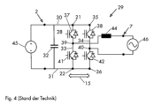
1b 電力コンバータ
1、48 昇圧コンバータ
2 入力
2a、2b 接続部
3 DC電圧ジェネレータ
4 チョーク
5 ダイオード
6 パワー半導体スイッチ
6a 第1パワー半導体スイッチ
7 出力
8 矢印
9 降圧コンバータ
10 DC電圧源
11 矢印
14、72、78 ハーフブリッジ構成
15 両方向矢印
16 DC電圧源
18 DC電圧源
20、33、34、20a、20b ハーフブリッジ
21、35、58 接続点
22、36、60、67 接続点
23、37、38、23a ハイサイドパワー半導体スイッチ
24、41、42、24a ローサイドパワー半導体スイッチ
25、44 チョーク
26、56 ダイオード
27 ダイオード
28 リンク回路
29 インバータ
30 リンク回路極
31 リンク回路極
32 リンク回路コンデンサ
39、40 分岐点
45 DC電圧ジェネレータ
46 AC電圧グリッド
49、73、49a、49b 駆動回路
50 クロックジェネレータ
51 制御入力
52、52a、52b 補助回路構成
53、74 供給コンデンサ
54 補助コンデンサ
55 補助半導体スイッチ
57 ブートストラップダイオード
59 基準電位接続
61 第1の接続
62 第2の接続
63 起動抵抗
64 駆動回路
65 比較回路
66 ツェナーダイオード
68 抵抗器
69 非反転入力
70 さらなる主接続
75 接続
76 さらなる接続
77 さらなるブートストラップダイオード
VVS 準備ステップ
VS1、VS2、VS3 方法ステップ
Claims (17)
- パワーエレクトロニクスデバイス(1a)、特に電力コンバータ(1b)であって、第1パワー半導体スイッチ(6a)と、当該第1パワー半導体スイッチ(6a)を駆動するための駆動回路(49、49a、49b)と、当該駆動回路(49、49a、49b)に電圧を供給するための電気的な補助回路構成(52、52a、52b)とを具え、前記補助回路構成(52、52a、52b)は、供給コンデンサ(53、53a、53b)と、補助コンデンサ(54)と、通常オフの補助半導体スイッチ(55、55a、55b)と、ダイオード(56)と、ブートストラップダイオード(57)とを具え、
前記補助半導体スイッチ(55、55a、55b)は、第1の接続点(58)を介して前記第1パワー半導体スイッチ(6a)の基準電位接続(59)に接続されており、
前記第1の接続点(58)を起点に、前記ダイオード(56)と、第2の接続点(60)と、前記補助コンデンサ(54)との直列接続が、前記補助半導体スイッチ(55、55a、55b)と並列に配置され、前記補助半導体スイッチ(55、55a、55b)がオフ状態にあるとき、前記補助コンデンサ(54)が前記第1パワー半導体スイッチ(6a)を通る電流によって充電され、
前記駆動回路(49、49a、49b)は、前記供給コンデンサ(53、53a、53b)に接続されて電圧供給され、
前記供給コンデンサ(53、53a、53b)は、第1の接続(61)によって前記ブートストラップダイオード(57)を介して前記第2の接続点(60)に、第2の接続(62)によって前記基準電位接続に電気的に接続され、前記補助半導体スイッチ(55、55a、55b)がオン状態にあり、前記補助コンデンサ(54)が少なくとも部分的に充電されている場合に、前記供給コンデンサ(53、53a、53b)が前記ブートストラップダイオード(57)を介して前記補助コンデンサ(54)によって充電され、
前記補助回路構成(52、52a、52b)が、前記補助コンデンサ(54)の充電電圧に基づいて、前記補助半導体スイッチ(55、55a、55b)の制御入力に前記補助半導体スイッチ(55、55a、55b)を切り替えるための制御信号を提供するように設計および構成された駆動回路(64)を具えることを特徴とするパワーエレクトロニクスデバイス。 - 前記駆動回路(64)は、前記補助コンデンサ(54)の充電電圧が第1の閾値を超えたときに、前記補助半導体スイッチ(55、55a、55b)の制御入力に、前記補助半導体スイッチ(55、55a、55b)をオン状態にする制御信号を提供し、前記補助コンデンサ(54)の充電電圧が前記第1の閾値よりも低い第2の閾値を下回ったときに、前記補助半導体スイッチ(55、55a、55b)の制御入力に、前記補助半導体スイッチ(55、55a、55b)をオフ状態にする制御信号を提供するように設計および構成されており、ここで前記第1の閾値は、少なくとも前記駆動回路(49、49a、49b)への供給電圧の大きさに対応する、請求項1に記載のパワーエレクトロニクスデバイス(1a)。
- 前記駆動回路(64)が、2レベルレギュレータ、特に比較回路(65)、あるいはモノフロップまたはPWMコントローラまたは周波数コントローラである、請求項1または2に記載のパワーエレクトロニクスデバイス(1a)。
- 前記駆動回路(64)は、前記補助コンデンサ(54)に電気的に接続されるように設計および構成され、前記補助コンデンサ(54)によって前記駆動回路(64)に電圧が供給される、請求項1から3のいずれか一項に記載のパワーエレクトロニクスデバイス(1a)。
- 前記補助半導体スイッチ(55、55a、55b)が、前記第1パワー半導体スイッチ(6a)と同じ極性を有する、請求項1から4のいずれか一項に記載のパワーエレクトロニクスデバイス(1a)。
- 前記第1パワー半導体スイッチ(6a)は、通常オフになるように設計されており、オフスイッチング状態において、電圧が前記第1パワー半導体スイッチ(6a)の基準電位接続(59)と前記パワー半導体スイッチ(6a)のさらなる主接続(70)の間に印加されたときにリーク電流がある、請求項1から5のいずれか一項に記載のパワーエレクトロニクスデバイス(1a)。
- 前記補助回路構成(52、52a、52b)、特に前記補助半導体スイッチ(55、55a、55b)が、前記駆動回路(49、49a、49b、73)の少なくとも1つに給電するためだけに機能する、請求項1から6のいずれか一項に記載のパワーエレクトロニクスデバイス(1a)。
- 前記駆動回路(49、49a、49b)は、クロックジェネレータ(50)と統合されるように設計されており、前記クロックジェネレータ(50)は、前記駆動回路(49、49a、49b)によって提供される制御信号のパルスパターンを生成する、請求項1から7のいずれか一項に記載のパワーエレクトロニクスデバイス(1a)。
- 第3の接続点(21)を起点に、ハイサイドパワー半導体スイッチ(23a)と、分岐点(39)と、ローサイドパワー半導体スイッチ(24a)とからなる直列接続を含むハーフブリッジ(20a、20b)および第4の接続点(22)を具え、前記第1パワー半導体スイッチ(6a)は前記ローサイドパワー半導体スイッチ(24a)であり、前記パワーエレクトロニクスデバイス(1a)は、特に、DC/DCコンバータまたはインバータ(29)である、請求項1から8のいずれか一項に記載のパワーエレクトロニクスデバイス(1a)。
- 1つまたは複数の直列接続または並列接続されたリンク回路コンデンサを介して、前記第3の接続点(21)を前記第4の接続点(22)に接続する電気接続を有するリンク回路(28)を具える、請求項9に記載のパワーエレクトロニクスデバイス(1a)。
- 前記ハイサイドパワー半導体スイッチ(23a)およびローサイドパワー半導体スイッチ(24a)の両方について、それぞれのパワー半導体スイッチを駆動するためのそれぞれの駆動回路(49a、49b)と、前記駆動回路(49a、49b)に電圧を供給するためのそれぞれ別個の電気的な補助回路構成(52a、52b)とを具え、前記ハイサイドパワー半導体スイッチ(23a)とローサイドパワー半導体スイッチ(24a)の両方がそれぞれ第1パワー半導体スイッチ(6a)として設計されている、請求項9または10に記載のパワーエレクトロニクスデバイス(1a)。
- 前記ハイサイドパワー半導体スイッチ(23a)を駆動するための駆動回路(73)と、この駆動回路(73)の電圧供給のための供給コンデンサ(74)と具え、前記供給コンデンサは、前記ローサイドパワー半導体スイッチ(24a)を駆動するための駆動回路(49)に電圧を供給するために、接続(75)によって前記ハイサイドパワー半導体スイッチ(23a)の基準電位接続(59)に電気的に接続され、さらなる接続(76)によって、さらなるブートストラップダイオード(77)を介して前記補助回路構成(52)に含まれる供給コンデンサ(53)の第1の接続(61)に電気的に接続されている、請求項9または10に記載のパワーエレクトロニクスデバイス(1a)。
- 前記ハイサイドパワー半導体スイッチ(23a)および前記ローサイドパワー半導体スイッチ(24a)が通常オフであり、オフスイッチング状態において、それらの基準電位接続(59)とそれらのさらなる主接続(70)との間に電圧が印加されたときにリーク電流を有する、請求項9から12のいずれか一項に記載のパワーエレクトロニクスデバイス(1a)。
- パワー半導体スイッチの駆動回路(49)に電圧を供給する方法であって、前記駆動回路(49、49a、49b)は、供給コンデンサ(53、53a、53b)によって電圧供給され、前記供給コンデンサ(53、53a、53b)を充電するために、補助コンデンサ(54)が、通常オフの補助スイッチのオフスイッチング状態の間に前記パワー半導体スイッチを流れる電流によって充電され、前記供給コンデンサ(53)が、前記通常オフの補助スイッチがオン状態のときに、前記補助コンデンサ(54)によって充電され、
前記補助スイッチは、前記補助コンデンサ(54)の充電電圧に基づいてオン状態にされることを特徴とする方法。 - 前記通常オフの補助スイッチは、前記パワー半導体の基準電位接続(59)に接続されており、第1の方法ステップ(VS1)において、前記補助スイッチがオフ状態にあるとき、前記パワー半導体スイッチを流れる電流の少なくとも一部が前記補助コンデンサに迂回され、少なくとも部分的にこれを充電し、第2の方法ステップ(VS2)において、前記補助スイッチはオン状態にされ、前記補助コンデンサの電荷の少なくとも一部を前記供給コンデンサへ放出し、第3の方法ステップ(VS3)において、前記補助スイッチはオフスイッチング状態に戻され、その結果、この3つの方法ステップを複数回繰り返すことにより、動作中に前記駆動回路に給電するために、電力が、前記供給コンデンサに供給される、請求項14に記載の方法。
- 前記補助コンデンサ(54)の充電電圧が第1の閾値を超えると前記補助スイッチがオン状態になり(VS2)、前記補助コンデンサ(54)の電圧が第2の閾値を下回ると前記補助スイッチがオフ状態になり(VS3)、ここで前記第2の閾値は前記第1の閾値よりも低い、請求項14に記載の方法。
- 前記方法は、請求項1から13のいずれか一項に記載のパワーエレクトロニクスデバイス(1a)を使用して実行される、請求項14から16のいずれか一項に記載の方法。
Applications Claiming Priority (3)
| Application Number | Priority Date | Filing Date | Title |
|---|---|---|---|
| DE102019104652.1 | 2019-02-25 | ||
| DE102019104652.1A DE102019104652B4 (de) | 2019-02-25 | 2019-02-25 | Leistungselektronische Vorrichtung und Verfahren zur elektrischen Spannungsversorgung einer Treiberschaltung eines Leistungshalbleiterschalters |
| PCT/EP2020/052618 WO2020173667A1 (de) | 2019-02-25 | 2020-02-03 | Leistungselektronische vorrichtung und verfahren zur elektrischen spannungsversorgung einer treiberschaltung eines leistungshalbleiterschalters |
Publications (2)
| Publication Number | Publication Date |
|---|---|
| JP2022521419A JP2022521419A (ja) | 2022-04-07 |
| JP7426397B2 true JP7426397B2 (ja) | 2024-02-01 |
Family
ID=69528788
Family Applications (1)
| Application Number | Title | Priority Date | Filing Date |
|---|---|---|---|
| JP2021549505A Active JP7426397B2 (ja) | 2019-02-25 | 2020-02-03 | パワー半導体スイッチの駆動回路に電圧を供給するためのパワーエレクトロニクスデバイスおよび方法 |
Country Status (6)
| Country | Link |
|---|---|
| US (1) | US11990826B2 (ja) |
| EP (1) | EP3931963B1 (ja) |
| JP (1) | JP7426397B2 (ja) |
| CN (1) | CN113632380B (ja) |
| DE (1) | DE102019104652B4 (ja) |
| WO (1) | WO2020173667A1 (ja) |
Families Citing this family (1)
| Publication number | Priority date | Publication date | Assignee | Title |
|---|---|---|---|---|
| CN117458842B (zh) * | 2023-12-26 | 2024-03-08 | 华羿微电子股份有限公司 | 一种半桥驱动电路 |
Citations (2)
| Publication number | Priority date | Publication date | Assignee | Title |
|---|---|---|---|---|
| US20100066175A1 (en) | 2008-09-13 | 2010-03-18 | Infineon Technologies Ag | Circuit assembly for gating a power semiconductor switch |
| US20180145668A1 (en) | 2016-11-22 | 2018-05-24 | Mosway Technologies Limited | Voltage clamping circuit |
Family Cites Families (9)
| Publication number | Priority date | Publication date | Assignee | Title |
|---|---|---|---|---|
| DE202008013397U1 (de) * | 2008-10-09 | 2010-03-25 | Tridonicatco Schweiz Ag | Treiberschaltung für eine Halbleiterlichtquelle (LED) |
| CH699884B1 (de) * | 2008-11-07 | 2012-04-13 | Eth Zuerich | Ansteuerschaltung für leistungelektronische Schalter. |
| KR101033933B1 (ko) * | 2008-12-30 | 2011-05-11 | 서울과학기술대학교 산학협력단 | 고승압비를 갖는 비절연 소프트 스위칭 dcdc 컨버터 |
| US8558584B2 (en) * | 2010-11-30 | 2013-10-15 | Infineon Technologies Ag | System and method for bootstrapping a switch driver |
| EP2515439A1 (en) * | 2011-04-18 | 2012-10-24 | Philips Intellectual Property & Standards GmbH | Semiconductor switch with reliable blackout behavior and low control power |
| DE102012220118A1 (de) * | 2012-11-05 | 2014-05-22 | Bombardier Transportation Gmbh | Schaltungsanordnung und Verfahren zum Betreiben einer Schaltungsanordnung |
| US9780690B2 (en) * | 2016-01-28 | 2017-10-03 | Infineon Technologies Austria Ag | Resonant decoupled auxiliary supply for a switched-mode power supply controller |
| CN107925345B (zh) * | 2016-02-16 | 2019-12-27 | 富士电机株式会社 | 半导体装置 |
| JP2018007403A (ja) * | 2016-07-01 | 2018-01-11 | 三菱電機株式会社 | 電力変換装置 |
-
2019
- 2019-02-25 DE DE102019104652.1A patent/DE102019104652B4/de active Active
-
2020
- 2020-02-03 EP EP20704449.6A patent/EP3931963B1/de active Active
- 2020-02-03 JP JP2021549505A patent/JP7426397B2/ja active Active
- 2020-02-03 WO PCT/EP2020/052618 patent/WO2020173667A1/de not_active Ceased
- 2020-02-03 CN CN202080016693.7A patent/CN113632380B/zh active Active
-
2021
- 2021-08-24 US US17/410,225 patent/US11990826B2/en active Active
Patent Citations (2)
| Publication number | Priority date | Publication date | Assignee | Title |
|---|---|---|---|---|
| US20100066175A1 (en) | 2008-09-13 | 2010-03-18 | Infineon Technologies Ag | Circuit assembly for gating a power semiconductor switch |
| US20180145668A1 (en) | 2016-11-22 | 2018-05-24 | Mosway Technologies Limited | Voltage clamping circuit |
Also Published As
| Publication number | Publication date |
|---|---|
| DE102019104652A1 (de) | 2020-08-27 |
| US20210384824A1 (en) | 2021-12-09 |
| DE102019104652B4 (de) | 2024-03-14 |
| WO2020173667A1 (de) | 2020-09-03 |
| EP3931963B1 (de) | 2022-08-17 |
| EP3931963A1 (de) | 2022-01-05 |
| CN113632380A (zh) | 2021-11-09 |
| CN113632380B (zh) | 2025-11-21 |
| JP2022521419A (ja) | 2022-04-07 |
| US11990826B2 (en) | 2024-05-21 |
Similar Documents
| Publication | Publication Date | Title |
|---|---|---|
| CN104052296B (zh) | 用于开关模式功率转换器的系统和方法 | |
| US8384236B2 (en) | Vehicle mounted converter | |
| US8487664B2 (en) | System and method for driving a switch | |
| US7486055B2 (en) | DC-DC converter having a diode module with a first series circuit and a second series with a flywheel diode | |
| US20120133420A1 (en) | System and Method for Bootstrapping a Switch Driver | |
| US11323031B2 (en) | Half-bridge driver circuit with a switched capacitor supply voltage for high side drive signal generation | |
| CN108696123A (zh) | 双向dc-dc转换器 | |
| KR20030019133A (ko) | Dc-dc 컨버터 | |
| CN102480216B (zh) | 用于驱动共源共栅开关的系统和方法 | |
| JPH118910A (ja) | ハイブリッド電気自動車の電源装置 | |
| KR101734210B1 (ko) | 양방향 직류-직류 컨버터 | |
| CN114097170B (zh) | 电源系统 | |
| JP5394975B2 (ja) | スイッチングトランジスタの制御回路およびそれを用いた電力変換装置 | |
| US9780690B2 (en) | Resonant decoupled auxiliary supply for a switched-mode power supply controller | |
| CN107615634A (zh) | 电力转换装置以及使用电力转换装置的电源系统 | |
| JP7426397B2 (ja) | パワー半導体スイッチの駆動回路に電圧を供給するためのパワーエレクトロニクスデバイスおよび方法 | |
| CN114514681B (zh) | Dcdc转换器 | |
| KR101030776B1 (ko) | 승압형 직류/직류 변환기 | |
| US10906484B2 (en) | In-vehicle power supply device | |
| US12261517B2 (en) | H-bridge circuit with bootstrap capacitor gate drive charging circuit | |
| JP6668056B2 (ja) | 電力変換装置、これを用いた電源システム及び自動車 | |
| JP6801343B2 (ja) | 電力変換器 | |
| JP6950495B2 (ja) | 電力変換器 | |
| EP2575246B1 (en) | Method for discharging a DC-link capacitor in a DC-DC converter apparatus, and corresponding DC-DC converter apparatus | |
| EP4335026A1 (en) | Power inverter and method for controlling a power inverter |
Legal Events
| Date | Code | Title | Description |
|---|---|---|---|
| A621 | Written request for application examination |
Free format text: JAPANESE INTERMEDIATE CODE: A621 Effective date: 20221021 |
|
| A131 | Notification of reasons for refusal |
Free format text: JAPANESE INTERMEDIATE CODE: A131 Effective date: 20230905 |
|
| A521 | Request for written amendment filed |
Free format text: JAPANESE INTERMEDIATE CODE: A523 Effective date: 20231117 |
|
| TRDD | Decision of grant or rejection written | ||
| A01 | Written decision to grant a patent or to grant a registration (utility model) |
Free format text: JAPANESE INTERMEDIATE CODE: A01 Effective date: 20240109 |
|
| A61 | First payment of annual fees (during grant procedure) |
Free format text: JAPANESE INTERMEDIATE CODE: A61 Effective date: 20240122 |
|
| R150 | Certificate of patent or registration of utility model |
Ref document number: 7426397 Country of ref document: JP Free format text: JAPANESE INTERMEDIATE CODE: R150 |