JP7426397B2 - Power electronic devices and methods for supplying voltage to drive circuits of power semiconductor switches - Google Patents
Power electronic devices and methods for supplying voltage to drive circuits of power semiconductor switches Download PDFInfo
- Publication number
- JP7426397B2 JP7426397B2 JP2021549505A JP2021549505A JP7426397B2 JP 7426397 B2 JP7426397 B2 JP 7426397B2 JP 2021549505 A JP2021549505 A JP 2021549505A JP 2021549505 A JP2021549505 A JP 2021549505A JP 7426397 B2 JP7426397 B2 JP 7426397B2
- Authority
- JP
- Japan
- Prior art keywords
- auxiliary
- semiconductor switch
- power semiconductor
- capacitor
- drive circuit
- Prior art date
- Legal status (The legal status is an assumption and is not a legal conclusion. Google has not performed a legal analysis and makes no representation as to the accuracy of the status listed.)
- Active
Links
Images


Classifications
-
- H—ELECTRICITY
- H03—ELECTRONIC CIRCUITRY
- H03K—PULSE TECHNIQUE
- H03K17/00—Electronic switching or gating, i.e. not by contact-making and –breaking
- H03K17/10—Modifications for increasing the maximum permissible switched voltage
- H03K17/107—Modifications for increasing the maximum permissible switched voltage in composite switches
-
- H—ELECTRICITY
- H02—GENERATION; CONVERSION OR DISTRIBUTION OF ELECTRIC POWER
- H02M—APPARATUS FOR CONVERSION BETWEEN AC AND AC, BETWEEN AC AND DC, OR BETWEEN DC AND DC, AND FOR USE WITH MAINS OR SIMILAR POWER SUPPLY SYSTEMS; CONVERSION OF DC OR AC INPUT POWER INTO SURGE OUTPUT POWER; CONTROL OR REGULATION THEREOF
- H02M1/00—Details of apparatus for conversion
- H02M1/0003—Details of control, feedback or regulation circuits
- H02M1/0006—Arrangements for supplying an adequate voltage to the control circuit of converters
-
- H—ELECTRICITY
- H02—GENERATION; CONVERSION OR DISTRIBUTION OF ELECTRIC POWER
- H02M—APPARATUS FOR CONVERSION BETWEEN AC AND AC, BETWEEN AC AND DC, OR BETWEEN DC AND DC, AND FOR USE WITH MAINS OR SIMILAR POWER SUPPLY SYSTEMS; CONVERSION OF DC OR AC INPUT POWER INTO SURGE OUTPUT POWER; CONTROL OR REGULATION THEREOF
- H02M1/00—Details of apparatus for conversion
- H02M1/08—Circuits specially adapted for the generation of control voltages for semiconductor devices incorporated in static converters
- H02M1/088—Circuits specially adapted for the generation of control voltages for semiconductor devices incorporated in static converters for the simultaneous control of series or parallel connected semiconductor devices
- H02M1/096—Circuits specially adapted for the generation of control voltages for semiconductor devices incorporated in static converters for the simultaneous control of series or parallel connected semiconductor devices the power supply of the control circuit being connected in parallel to the main switching element
-
- H—ELECTRICITY
- H02—GENERATION; CONVERSION OR DISTRIBUTION OF ELECTRIC POWER
- H02M—APPARATUS FOR CONVERSION BETWEEN AC AND AC, BETWEEN AC AND DC, OR BETWEEN DC AND DC, AND FOR USE WITH MAINS OR SIMILAR POWER SUPPLY SYSTEMS; CONVERSION OF DC OR AC INPUT POWER INTO SURGE OUTPUT POWER; CONTROL OR REGULATION THEREOF
- H02M3/00—Conversion of DC power input into DC power output
- H02M3/02—Conversion of DC power input into DC power output without intermediate conversion into AC
- H02M3/04—Conversion of DC power input into DC power output without intermediate conversion into AC by static converters
- H02M3/10—Conversion of DC power input into DC power output without intermediate conversion into AC by static converters using discharge tubes with control electrode or semiconductor devices with control electrode
- H02M3/145—Conversion of DC power input into DC power output without intermediate conversion into AC by static converters using discharge tubes with control electrode or semiconductor devices with control electrode using devices of a triode or transistor type requiring continuous application of a control signal
- H02M3/155—Conversion of DC power input into DC power output without intermediate conversion into AC by static converters using discharge tubes with control electrode or semiconductor devices with control electrode using devices of a triode or transistor type requiring continuous application of a control signal using semiconductor devices only
-
- H—ELECTRICITY
- H03—ELECTRONIC CIRCUITRY
- H03K—PULSE TECHNIQUE
- H03K17/00—Electronic switching or gating, i.e. not by contact-making and –breaking
- H03K17/51—Electronic switching or gating, i.e. not by contact-making and –breaking characterised by the components used
- H03K17/56—Electronic switching or gating, i.e. not by contact-making and –breaking characterised by the components used by the use, as active elements, of semiconductor devices
- H03K17/567—Circuits characterised by the use of more than one type of semiconductor device, e.g. BIMOS, composite devices such as IGBT
-
- H—ELECTRICITY
- H02—GENERATION; CONVERSION OR DISTRIBUTION OF ELECTRIC POWER
- H02M—APPARATUS FOR CONVERSION BETWEEN AC AND AC, BETWEEN AC AND DC, OR BETWEEN DC AND DC, AND FOR USE WITH MAINS OR SIMILAR POWER SUPPLY SYSTEMS; CONVERSION OF DC OR AC INPUT POWER INTO SURGE OUTPUT POWER; CONTROL OR REGULATION THEREOF
- H02M3/00—Conversion of DC power input into DC power output
- H02M3/02—Conversion of DC power input into DC power output without intermediate conversion into AC
- H02M3/04—Conversion of DC power input into DC power output without intermediate conversion into AC by static converters
- H02M3/10—Conversion of DC power input into DC power output without intermediate conversion into AC by static converters using discharge tubes with control electrode or semiconductor devices with control electrode
- H02M3/145—Conversion of DC power input into DC power output without intermediate conversion into AC by static converters using discharge tubes with control electrode or semiconductor devices with control electrode using devices of a triode or transistor type requiring continuous application of a control signal
- H02M3/155—Conversion of DC power input into DC power output without intermediate conversion into AC by static converters using discharge tubes with control electrode or semiconductor devices with control electrode using devices of a triode or transistor type requiring continuous application of a control signal using semiconductor devices only
- H02M3/156—Conversion of DC power input into DC power output without intermediate conversion into AC by static converters using discharge tubes with control electrode or semiconductor devices with control electrode using devices of a triode or transistor type requiring continuous application of a control signal using semiconductor devices only with automatic control of output voltage or current, e.g. switching regulators
- H02M3/158—Conversion of DC power input into DC power output without intermediate conversion into AC by static converters using discharge tubes with control electrode or semiconductor devices with control electrode using devices of a triode or transistor type requiring continuous application of a control signal using semiconductor devices only with automatic control of output voltage or current, e.g. switching regulators including plural semiconductor devices as final control devices for a single load
-
- H—ELECTRICITY
- H03—ELECTRONIC CIRCUITRY
- H03K—PULSE TECHNIQUE
- H03K2217/00—Indexing scheme related to electronic switching or gating, i.e. not by contact-making or -breaking covered by H03K17/00
- H03K2217/0063—High side switches, i.e. the higher potential [DC] or life wire [AC] being directly connected to the switch and not via the load
-
- H—ELECTRICITY
- H03—ELECTRONIC CIRCUITRY
- H03K—PULSE TECHNIQUE
- H03K2217/00—Indexing scheme related to electronic switching or gating, i.e. not by contact-making or -breaking covered by H03K17/00
- H03K2217/0072—Low side switches, i.e. the lower potential [DC] or neutral wire [AC] being directly connected to the switch and not via the load
-
- H—ELECTRICITY
- H03—ELECTRONIC CIRCUITRY
- H03K—PULSE TECHNIQUE
- H03K2217/00—Indexing scheme related to electronic switching or gating, i.e. not by contact-making or -breaking covered by H03K17/00
- H03K2217/0081—Power supply means, e.g. to the switch driver
Landscapes
- Engineering & Computer Science (AREA)
- Power Engineering (AREA)
- Dc-Dc Converters (AREA)
- Power Conversion In General (AREA)
- Electronic Switches (AREA)
- Physics & Mathematics (AREA)
- Nonlinear Science (AREA)
Description
本発明は、少なくとも1つの第1パワー半導体スイッチを有するパワーエレクトロニクスデバイス、特に電力コンバータに関する。また、第1パワー半導体スイッチを駆動するために、パワーエレクトロニクスデバイスは駆動回路を備える。 The present invention relates to a power electronic device, in particular a power converter, having at least one first power semiconductor switch. The power electronics device also includes a drive circuit for driving the first power semiconductor switch.
本発明はまた、パワー半導体スイッチの駆動回路に電圧を供給するための方法に関する。 The invention also relates to a method for supplying voltage to a drive circuit of a power semiconductor switch.
パワーエレクトロニクスデバイスは、例えば、降圧コンバータ、昇圧コンバータ、または昇圧/降圧コンバータあるいはインバータであり得る。このような電力コンバータは、入力側に存在する電圧を変換するために電力コンバータによって適宜切り替えられるパワー半導体スイッチを備える。このパワー半導体スイッチを駆動するために、制御信号がパワー半導体スイッチの制御入力に印加される。制御入力は、例えば、IGBT(絶縁ゲートバイポーラトランジスタ)またはMOSFET(金属酸化膜半導体電界効果トランジスタ)のゲート接続であり得る。マイクロプロセッサなどの集積回路(クロックジェネレータや信号ジェネレータとも呼ばれる)が、パワー半導体スイッチの駆動信号を生成するためによく使用される。しかしながら、これらの集積回路が供給する出力電流や出力電圧は、ほとんどの場合、パワー半導体スイッチを直接駆動するのに十分ではない。そこで、クロックジェネレータとパワー半導体スイッチとの間に駆動回路(ドライバ回路)を設け、クロックジェネレータの駆動信号から十分な電流と電圧の制御信号を生成し、ドライバ出力でパワー半導体スイッチの制御入力に前記制御信号を供給するようにしている。駆動信号および制御信号は、いわゆるパルス幅変調された駆動/制御信号であり得る。ここで、駆動/制御信号のパルスパターンは、変調変数および制御変数を介してクロックジェネレータで生成することができる。変調変数は、周期的、三角形、または鋸歯状の電圧プロファイルを有することができ、制御変数は、制御変数に対応する電圧値で一定のコースを有し得る。パルス幅変調駆動信号のパルスパターンは、制御変数と変調変数との比較を通じて生成することができ、クロックジェネレータは、変調変数の周波数および大きさと制御値の大きさに関して、電力コンバータの現在の動作状態に従って、例えば電力コンバータのコントローラによって制御される。別の方法として、制御信号は、固定のデューティサイクルを有するか、従属電流制御(電流モード)を介して生成されるか、またはスイッチング閾値および/または固定のオンまたはオフ時間に応じて他の方法で生成されてもよく、ここでスイッチング周波数も可変であり得る。クロックジェネレータと駆動回路は、共通の部品に組み込まれてもよい。それらを保護するために、または逆導通機能のために、パワー半導体スイッチは、それぞれボディダイオードを有するか、極性がボディダイオードに対応するダイオードを有し得る。 The power electronics device may be, for example, a buck converter, a boost converter, or a step-up/step-down converter or an inverter. Such a power converter comprises a power semiconductor switch which is suitably switched by the power converter in order to convert the voltage present on the input side. In order to drive this power semiconductor switch, a control signal is applied to a control input of the power semiconductor switch. The control input can be, for example, a gate connection of an IGBT (insulated gate bipolar transistor) or a MOSFET (metal oxide semiconductor field effect transistor). Integrated circuits such as microprocessors (also called clock generators or signal generators) are often used to generate drive signals for power semiconductor switches. However, the output currents and voltages provided by these integrated circuits are often not sufficient to directly drive power semiconductor switches. Therefore, a drive circuit (driver circuit) is provided between the clock generator and the power semiconductor switch, and sufficient current and voltage control signals are generated from the drive signal of the clock generator, and the driver output is applied to the control input of the power semiconductor switch. A control signal is supplied. The drive and control signals may be so-called pulse width modulated drive/control signals. Here, the pulse pattern of the drive/control signal can be generated by a clock generator via a modulation variable and a control variable. The modulation variable may have a periodic, triangular, or sawtooth voltage profile, and the control variable may have a constant course with a voltage value corresponding to the control variable. The pulse pattern of the pulse width modulated drive signal can be generated through a comparison of the control variable and the modulation variable, and the clock generator determines the current operating state of the power converter with respect to the frequency and magnitude of the modulation variable and the magnitude of the control value. eg by a controller of a power converter. Alternatively, the control signal has a fixed duty cycle or is generated via dependent current control (current mode) or other methods depending on switching thresholds and/or fixed on or off times. may be generated, where the switching frequency may also be variable. The clock generator and drive circuit may be integrated into a common component. In order to protect them or for the reverse conduction function, the power semiconductor switches each have a body diode or can have a diode whose polarity corresponds to the body diode.
電気機器の動作中および起動時の両方で、必要な構成要素、例えば電力コンバータのコントローラやそのパワー半導体スイッチの駆動回路に電力を供給する必要がある。電力コンバータの起動時に、例えば、電力コンバータの入力の第1接続部と第2接続部の間にDC電圧が印加され、このDC電圧は、例えば太陽電池モジュールやこのようなモジュールの直列接続(ストリング)などのDCジェネレータによって提供される。このように印加されたDC電圧は、例えば起動時に必要な構成要素に給電するために使用され得る。 Both during operation and during start-up of electrical equipment, it is necessary to supply power to the necessary components, such as the controller of the power converter and the drive circuit of its power semiconductor switch. During start-up of the power converter, a DC voltage is applied, for example, between a first connection and a second connection of the input of the power converter; ) and other DC generators. The DC voltage applied in this way can be used, for example, to power the necessary components during start-up.
本発明は、パワーエレクトロニクスデバイスの少なくとも1つの駆動回路への電圧の供給に関する。本発明はまた、パワー半導体スイッチの駆動回路に電圧を供給するための方法に関する。例えばMOSFETやIGBTなどのパワー半導体スイッチ用の駆動回路は、パワー半導体スイッチの基準電位接続の電位に関連して、通常10~20ボルトの電圧供給を必要とする。基準電位接続は、例えば、バイポーラトランジスタやIGBTの場合はエミッタ接続、MOSFETの場合はソース接続となる。パワー半導体スイッチの駆動回路は、電力コンバータのオンボード電源の起動前から動作する必要があり、またはオンボード電源の一部となっているため、特に供給が困難である。 The present invention relates to the supply of voltage to at least one drive circuit of a power electronic device. The invention also relates to a method for supplying voltage to a drive circuit of a power semiconductor switch. Drive circuits for power semiconductor switches, such as MOSFETs or IGBTs, for example, typically require a voltage supply of 10 to 20 volts in relation to the potential of the reference potential connection of the power semiconductor switch. The reference potential connection is, for example, an emitter connection in the case of a bipolar transistor or an IGBT, and a source connection in the case of a MOSFET. Drive circuits for power semiconductor switches are particularly difficult to supply because they must be operational before the on-board power supply of the power converter is started, or are part of the on-board power supply.
フライバックコンバータなどの電力コンバータの入力電圧から高抵抗の抵抗を介して駆動回路(PWMコントローラ)を内蔵したクロックジェネレータの供給コンデンサを充電し、並列ツェナーダイオードを介してコンデンサ電圧を制限することが知られている。しかしこの方式は効率が悪く、例えば400Vの入力電圧と15Vの必要なドライバ電圧では、わずか15V/400V=3.8%の効率しか得られない。したがって、この既知の構成は、フライバックコンバータの起動にしか適していない。 It is known that the supply capacitor of a clock generator with a built-in drive circuit (PWM controller) is charged from the input voltage of a power converter such as a flyback converter through a high-resistance resistor, and the capacitor voltage is limited through a parallel Zener diode. It is being However, this scheme is inefficient; for example, with an input voltage of 400V and a required driver voltage of 15V, an efficiency of only 15V/400V=3.8% can be obtained. This known configuration is therefore only suitable for starting flyback converters.
本発明は、冒頭で述べたタイプのパワーエレクトロニクスデバイス、特に冒頭で述べたタイプの電力コンバータ、および冒頭で述べたタイプの方法を規定するという目的に基づいている。これにより、パワーエレクトロニクスデバイスまたはパワー半導体スイッチの少なくとも1つの動作モードに適した方法で、パワー半導体スイッチの少なくとも1つの駆動回路に電圧を供給することが可能になる。 The invention is based on the object of providing a power electronics device of the type mentioned in the introduction, in particular a power converter of the type mentioned in the introduction, and a method of the type mentioned in the introduction. This makes it possible to supply the at least one drive circuit of the power semiconductor switch with a voltage in a manner that is suitable for the at least one operating mode of the power electronic device or the power semiconductor switch.
本発明によれば、この目的は、冒頭で述べたタイプのパワーエレクトロニクスデバイスの場合、駆動回路に電圧を供給するための電気補助回路構成を含み、この補助回路構成が、供給コンデンサと補助コンデンサ、通常オフの補助半導体スイッチ、ダイオード、およびブートストラップダイオードで構成されることによって達成される。この場合、補助半導体スイッチは、第1の接続点を介して第1パワー半導体スイッチの基準電位接続部に接続される。第1の接続点を起点に、ダイオード、第2の接続点、補助コンデンサの直列接続が、補助半導体スイッチと並列に配置され、補助半導体スイッチがオフ状態のときに、パワー半導体スイッチを流れる電流によって補助コンデンサが充電されるようになっている。その電圧供給のために、駆動回路は供給コンデンサに接続され、この供給コンデンサは、第1の接続部がブートストラップダイオードを介して第2の接続部に、第2の接続部が基準電位接続部にそれぞれ電気的に接続され、それによって、補助半導体スイッチがオン状態にあり、補助コンデンサが少なくとも部分的に充電されている場合、供給コンデンサが、ブートストラップダイオードを介して補助コンデンサによって充電される。 According to the invention, this object comprises, in the case of a power electronics device of the type mentioned at the outset, an electrical auxiliary circuit arrangement for supplying voltage to the drive circuit, which auxiliary circuit arrangement comprises a supply capacitor and an auxiliary capacitor; This is accomplished by consisting of a normally off auxiliary semiconductor switch, a diode, and a bootstrap diode. In this case, the auxiliary semiconductor switch is connected via a first connection point to a reference potential connection of the first power semiconductor switch. Starting from the first connection point, a series connection of a diode, a second connection point and an auxiliary capacitor is arranged in parallel with the auxiliary semiconductor switch, so that when the auxiliary semiconductor switch is in the off state, the current flowing through the power semiconductor switch The auxiliary capacitor is now charged. For its voltage supply, the drive circuit is connected to a supply capacitor, which has a first connection via a bootstrap diode to a second connection and a second connection to a reference potential connection. , respectively, such that the supply capacitor is charged by the auxiliary capacitor via the bootstrap diode when the auxiliary semiconductor switch is in the on state and the auxiliary capacitor is at least partially charged.
本発明によれば、この目的は、冒頭で述べたタイプのパワーエレクトロニクスデバイスの場合、パワーエレクトロニクスデバイスの主機能のために主回路に統合された補助スイッチを含む補助回路を用いて達成される。例として、電力コンバータの主機能は、電流を整流することである。この場合の補助スイッチは、第1パワー半導体スイッチの駆動回路、および場合によってはさらなるパワー半導体スイッチの駆動回路に電力を供給するためにのみ機能し、主機能を果たす第1パワー半導体スイッチとは対照的に、パワーエレクトロニクスデバイスまたは電力コンバータの主機能に全くまたは本質的に影響を与えない。補助コンデンサから供給コンデンサを充電するために補助スイッチが閉じている(つまりオン状態にある)期間は、オン状態の補助スイッチが本質的に電気接続のように動作するので、いかなる場合でもパワーエレクトロニクスデバイスまたは電力コンバータのこの主機能に干渉しない。パワーエレクトロニクスデバイスまたは電力コンバータの起動時、つまり休止状態のパワーエレクトロニクスデバイスまたは電力コンバータの起動プロセス中に、例えばDCジェネレータからのDC電圧がパワーエレクトロニクスデバイスの入力に印加されるため、基準電位接続と第1パワー半導体スイッチのさらなる主接続との間で、DC電圧が第1パワー半導体スイッチに印加される。起動時に、補助スイッチは、起動時にまだ存在しないため、パワーエレクトロニクスデバイスまたは電力コンバータ自体の主機能に干渉することはない。パワーエレクトロニクスデバイスまたは電力コンバータの動作中、第1パワー半導体スイッチは高周波数で切り替えられる。第1パワー半導体スイッチがオフ状態にある場合、つまりオン状態にない場合、補助スイッチは、そのスイッチ状態に応じて、電気接続の一部分のように、または第1パワー半導体スイッチ自体のように動作し、補助スイッチのそれぞれのスイッチング状態に関係なく、パワーエレクトロニクスデバイスまたは電力コンバータの主機能が影響を受けないようにすることができる。第1パワー半導体スイッチが閉じている場合、すなわちオン状態である場合、主回路の電力経路の電流は第1パワー半導体スイッチを通って流れる。駆動回路のエネルギー需要は低いため、またその電流のため、補助スイッチがオフ状態にある時間間隔が十分に短く保たれ、主機能に大きな影響を与えないようにするため、主回路は補助装置の充電によって大きく影響されない。 According to the invention, this object is achieved in the case of a power electronics device of the type mentioned at the outset with an auxiliary circuit comprising an auxiliary switch integrated into the main circuit for the main function of the power electronics device. As an example, the main function of a power converter is to rectify current. The auxiliary switch in this case serves only to supply power to the drive circuit of the first power semiconductor switch and possibly further power semiconductor switches, in contrast to the first power semiconductor switch which performs the main function. essentially have no or essentially no effect on the main functionality of the power electronics device or power converter. During the period when the auxiliary switch is closed (i.e. in the on state) to charge the supply capacitor from the auxiliary capacitor, the auxiliary switch in the on state essentially behaves like an electrical connection, so the power electronics device or not interfere with this main function of the power converter. During start-up of a power electronics device or power converter, i.e. during the start-up process of a dormant power electronics device or power converter, a DC voltage, for example from a DC generator, is applied to the input of the power electronics device, so that the reference potential connection and the A DC voltage is applied to the first power semiconductor switch between a further main connection of the first power semiconductor switch. At start-up, the auxiliary switch does not interfere with the main function of the power electronic device or the power converter itself, since it is not yet present at start-up. During operation of the power electronic device or power converter, the first power semiconductor switch is switched at high frequency. When the first power semiconductor switch is in the off state, i.e. not in the on state, the auxiliary switch acts either like part of the electrical connection or like the first power semiconductor switch itself, depending on its switch state. , regardless of the respective switching states of the auxiliary switches, the main function of the power electronics device or power converter may be unaffected. When the first power semiconductor switch is closed, ie in the on state, the current of the power path of the main circuit flows through the first power semiconductor switch. Due to the low energy demand of the drive circuit and due to its current, the main circuit is connected to the auxiliary equipment in order to ensure that the time interval during which the auxiliary switch is in the off state is kept short enough and does not significantly affect the main function. Not significantly affected by charging.
起動時に、補助コンデンサは、第1パワー半導体スイッチと第1のダイオードを介して充電することができ、ここで第1パワー半導体スイッチは、通常オンまたは通常オフであり得る。いずれの場合も、第1パワー半導体スイッチは、オフスイッチング状態でリーク電流を発生し得る。通常、第1パワー半導体スイッチは通常オフであり、オフスイッチング状態では、パワー半導体スイッチの2つの主接続、すなわち基準電位接続とパワー半導体スイッチのさらなる主接続の間に電圧が印加されるとリーク電流が生じる。リーク電流は、適切な電圧が存在する場合に、パワー半導体スイッチがオフにされたときに部品を流れる残留電流である。この残留電流は、パワー半導体スイッチを通る正規の流れ方向に流れるか、またはパワー半導体スイッチのボディダイオード、またはパワー半導体スイッチに含まれボディダイオードと同じ極性を有する補助ダイオードを通る逆方向に流れる。パワーエレクトロニクスデバイスまたは電力コンバータの動作中、補助コンデンサも同様に、第1パワー半導体スイッチがオフ状態にある期間と、第1パワー半導体スイッチがオン状態にある期間に、第1パワー半導体スイッチのリーク電流を介して、第1パワー半導体スイッチを定常的に流れる電流の割合によって充電され得る。補助半導体スイッチがオンになるたびに、補助コンデンサはその電荷の少なくとも一部を供給コンデンサに放出し、実際の駆動回路がそこから給電できるようにする。起動時の供給コンデンサの充電時間を短縮するために、供給コンデンサと補助コンデンサに追加の充電電流が供給されるように、起動抵抗器を追加で配置してもよい。起動抵抗器の1つの接続は、例えば、第1パワー半導体スイッチのさらなる主接続に電気的に接続され、起動抵抗器の第2の接続は、駆動回路の供給コンデンサの第1の接続に電気的に接続され得る。 During start-up, the auxiliary capacitor may be charged via the first power semiconductor switch and the first diode, where the first power semiconductor switch may be normally on or normally off. In either case, the first power semiconductor switch may generate leakage current in the off-switching state. Normally, the first power semiconductor switch is normally off, and in the off-switching state leakage current occurs when a voltage is applied between the two main connections of the power semiconductor switch, namely the reference potential connection and the further main connection of the power semiconductor switch. occurs. Leakage current is the residual current that flows through a component when a power semiconductor switch is turned off, provided a suitable voltage is present. This residual current flows either in the normal flow direction through the power semiconductor switch or in the reverse direction through a body diode of the power semiconductor switch or an auxiliary diode included in the power semiconductor switch and having the same polarity as the body diode. During operation of the power electronic device or power converter, the auxiliary capacitor likewise absorbs the leakage current of the first power semiconductor switch during the period when the first power semiconductor switch is in the OFF state and during the period when the first power semiconductor switch is in the ON state. The first power semiconductor switch can be charged by a constant rate of current flowing through the first power semiconductor switch. Each time the auxiliary semiconductor switch is turned on, the auxiliary capacitor releases at least part of its charge to the supply capacitor, allowing the actual drive circuit to be powered therefrom. To reduce the charging time of the supply capacitor during start-up, an additional start-up resistor may be arranged so that additional charging current is provided to the supply capacitor and the auxiliary capacitor. One connection of the starting resistor is electrically connected to a further main connection of the first power semiconductor switch, for example, and a second connection of the starting resistor is electrically connected to a first connection of the supply capacitor of the drive circuit. can be connected to.
本発明によれば、補助コンデンサから供給コンデンサを充電することによって第1パワー半導体スイッチの駆動回路に電圧が供給され、補助コンデンサは、パワーエレクトロニクスデバイスまたは電力コンバータの動作中に、第1パワー半導体スイッチを流れる電流(リーク電流または第1パワー半導体スイッチがオン状態にあるときの電流)によって充電される。本発明のパワーエレクトロニクスデバイスまたは本発明の電力コンバータは、第1パワー半導体スイッチの駆動回路に電圧を供給することが可能であり、その電圧供給は、その良好な効率により、パワーエレクトロニクスデバイスまたは電力コンバータの起動時と動作中の両方に適している。 According to the invention, voltage is supplied to the drive circuit of the first power semiconductor switch by charging the supply capacitor from the auxiliary capacitor, the auxiliary capacitor being able to supply voltage to the drive circuit of the first power semiconductor switch during operation of the power electronic device or the power converter. (leakage current or current when the first power semiconductor switch is in the on state) flows through the first power semiconductor switch. The power electronic device of the invention or the power converter of the invention is capable of supplying voltage to the drive circuit of the first power semiconductor switch, which voltage supply, due to its good efficiency, Suitable both at startup and during operation.
電力コンバータの主機能のための第1パワー半導体スイッチを有する主回路へ補助回路構成の補助スイッチを組み込むのを説明するために、例示的な実施形態による電力コンバータは、入力および出力を有し、ここで第3の接続点が入力の第1の接続部に電気的に接続され、第4の接続点が入力の第2の接続部に接続され、第1の接続分岐が第3の接続点から第4の接続点まで延びる。例示的な実施形態によれば、第3の接続点から出発して、第1の接続分岐は、第1パワー半導体スイッチ、第1の接続点、および通常オフの補助スイッチを直列接続で有する。例示的な実施形態によれば、第2の電気接続分岐は、第4の接続点から第5の接続点まで延在し、第4の接続点から出発して、補助コンデンサ、第2の接続点、ダイオード、第1の接続点、および供給コンデンサを直列で有し、第5および第2の接続点は、ブートストラップダイオードを介して第2の接続分岐と並列に電気的に接続されている。例示的な実施形態によれば、電力コンバータは、ドライバ出力が第1パワー半導体スイッチの制御入力に電気的に接続された駆動回路をさらに含み、この駆動回路は、その電圧供給用の供給コンデンサと並列に接続されている。例示的な実施形態によれば、電力コンバータはまた、比較器出力が補助スイッチの制御入力に接続された比較器回路を具えてもよく、この比較器回路は、補助コンデンサの充電電圧に基づいてその比較器出力に制御信号を提供するように設計される。ここでダイオードの順方向は、電力コンバータの少なくとも1つの第1の動作状態において、補助スイッチがオフ状態のときにダイオードおよび第1パワー半導体スイッチを介して補助コンデンサが充電されるように構成され、ブートストラップダイオードの順方向は、少なくとも1つの第2の動作状態において、補助スイッチがオン状態にあるときに供給コンデンサがブートストラップダイオードを介して補助コンデンサによって充電されるように構成される。 To illustrate the incorporation of the auxiliary switch of the auxiliary circuitry into the main circuit with the first power semiconductor switch for the main function of the power converter, the power converter according to an exemplary embodiment has an input and an output; where the third connection point is electrically connected to the first connection of the input, the fourth connection point is connected to the second connection of the input, and the first connection branch is connected to the third connection point. to the fourth connection point. According to an exemplary embodiment, starting from the third connection point, the first connection branch has a first power semiconductor switch, a first connection point and a normally off auxiliary switch in series connection. According to an exemplary embodiment, the second electrical connection branch extends from the fourth connection point to the fifth connection point, and starting from the fourth connection point, the auxiliary capacitor, the second connection a point, a diode, a first connection point and a supply capacitor in series, the fifth and second connection points being electrically connected in parallel with the second connection branch via a bootstrap diode. . According to an exemplary embodiment, the power converter further includes a drive circuit whose driver output is electrically connected to a control input of the first power semiconductor switch, the drive circuit having a supply capacitor for its voltage supply. connected in parallel. According to an exemplary embodiment, the power converter may also include a comparator circuit whose comparator output is connected to the control input of the auxiliary switch, and the comparator circuit is configured to It is designed to provide a control signal to its comparator output. The forward direction of the diode is here configured such that in at least one first operating state of the power converter, the auxiliary capacitor is charged via the diode and the first power semiconductor switch when the auxiliary switch is in the off state; The forward direction of the bootstrap diode is configured such that in at least one second operating state, the supply capacitor is charged by the auxiliary capacitor via the bootstrap diode when the auxiliary switch is in the on state.
本発明の有利な実施形態は、以下の説明および従属請求項に記載されており、その特徴は、個別に、および互いに任意の組み合わせで適用することができる。 Advantageous embodiments of the invention are described in the following description and in the dependent claims, the features of which can be applied individually and in any combination with one another.
有利には、補助回路構成は、補助コンデンサの充電電圧に基づいて補助半導体スイッチの制御入力で補助半導体スイッチを切り替えるための制御信号を提供するように設計および構成された駆動回路を具え得る。 Advantageously, the auxiliary circuit arrangement may comprise a drive circuit designed and configured to provide a control signal for switching the auxiliary semiconductor switch at a control input of the auxiliary semiconductor switch based on the charging voltage of the auxiliary capacitor.
補助スイッチは通常オフであるため、補助コンデンサは最初に第1パワー半導体スイッチを介して充電され、制御信号は補助コンデンサから供給コンデンサを充電するためにのみ、駆動回路によって補助スイッチの制御入力に提供されなければならないので、駆動回路は補助コンデンサから自身の電圧供給を得ることができる。補助スイッチは、補助コンデンサが駆動回路に給電するのに十分な電圧まで充電されると閉じ、充電電圧が低くなると再び開く(ヒステリシス)ことができ、補助コンデンサが、補助スイッチがオン状態にあるときはいつでも、ブートストラップ原理に従ってブートストラップダイオードを介して、第1パワー半導体スイッチの駆動回路用の供給コンデンサに給電する。補助回路構成は、第1パワー半導体スイッチが最初にオン状態になった後、供給コンデンサが充電されて駆動回路に供給され、その結果、第1パワー半導体スイッチがクロック駆動されると、高い電流が補助回路に流れ、補助コンデンサと供給コンデンサが継続的に再充電されるように設計され得る。駆動回路は、特に、補助コンデンサの充電電圧が第1の閾値を超えると、補助スイッチをオン状態にする制御信号をその制御入力に提供するように設計および構成され得る。第1の閾値は、駆動回路の供給電圧に対応するか、実質的に対応している。本出願の文脈において、「駆動回路の供給電圧」という用語は、駆動回路に印加される電圧や、駆動回路用の供給コンデンサによって提供される電圧を意味するものではなく、むしろ駆動回路で使用されるコンポーネントに依存して、第1パワー半導体スイッチを駆動するのに適した電圧値を意味する。駆動回路の供給電圧は、例えば、構成要素に由来する駆動回路の最小供給電圧と構成要素に由来する最大供給電圧との間であってもよいし、構成要素に由来する所定の電圧値であってもよく、特に、駆動回路に供給するための第1パワー半導体スイッチに基づいて適切に選択された電圧値であり得る。補助スイッチおよび補助回路構成は、補助スイッチがオン状態になることによって第1の閾値に達したときに過度に高い電圧から保護されるので、補助回路構成のすべての構成要素は、このより低い電圧以下のためにのみ設計することができ、補助回路構成に安価なコンポーネントを使用することが可能になる。 Since the auxiliary switch is normally off, the auxiliary capacitor is first charged through the first power semiconductor switch, and the control signal is provided by the drive circuit to the control input of the auxiliary switch only to charge the supply capacitor from the auxiliary capacitor. so that the drive circuit can derive its own voltage supply from the auxiliary capacitor. The auxiliary switch closes when the auxiliary capacitor is charged to a voltage sufficient to power the drive circuit, and can open again (hysteresis) when the charging voltage drops, and the auxiliary capacitor closes when the auxiliary switch is in the on state. always supplies the supply capacitor for the drive circuit of the first power semiconductor switch via the bootstrap diode according to the bootstrap principle. The auxiliary circuit arrangement is such that after the first power semiconductor switch is first turned on, the supply capacitor is charged and supplied to the drive circuit, so that when the first power semiconductor switch is clocked, a high current is generated. The auxiliary circuit may be designed to continuously recharge the auxiliary capacitor and the supply capacitor. The drive circuit may be particularly designed and configured to provide at its control input a control signal that turns on the auxiliary switch when the charging voltage of the auxiliary capacitor exceeds a first threshold value. The first threshold value corresponds or substantially corresponds to the supply voltage of the drive circuit. In the context of this application, the term "drive circuit supply voltage" does not mean the voltage applied to the drive circuit or the voltage provided by the supply capacitor for the drive circuit, but rather the voltage used in the drive circuit. means a voltage value suitable for driving the first power semiconductor switch depending on the components involved. The supply voltage of the drive circuit may be, for example, between the minimum supply voltage of the drive circuit originating from the component and the maximum supply voltage originating from the component, or it may be a predetermined voltage value originating from the component. In particular, the voltage value may be suitably selected based on the first power semiconductor switch for supplying the drive circuit. The auxiliary switch and the auxiliary circuitry are protected from excessively high voltages when the first threshold is reached by the auxiliary switch being in the on state, so that all components of the auxiliary circuitry are protected from this lower voltage. It is possible to design only for the following, making it possible to use inexpensive components for the auxiliary circuitry.
駆動回路は、補助コンデンサの充電電圧が第1の閾値を超えたときに補助半導体スイッチの制御入力で補助半導体スイッチをオン状態にする制御信号を提供し、補助コンデンサの充電電圧が第1の閾値よりも低い第2の閾値を下回ったときに補助半導体スイッチの制御入力で補助半導体スイッチをオフ状態にする制御信号を提供するように設計および構成されていることも有利であり得る。ここで、第1の閾値は、少なくとも駆動回路の供給電圧に対応する。 The drive circuit provides a control signal for turning on the auxiliary semiconductor switch at a control input of the auxiliary semiconductor switch when the charging voltage of the auxiliary capacitor exceeds a first threshold value, It may also be advantageous to be designed and arranged to provide a control signal at the control input of the auxiliary semiconductor switch to turn the auxiliary semiconductor switch off when a second threshold value lower than . Here, the first threshold corresponds to at least the supply voltage of the drive circuit.
補助スイッチは通常オフの補助スイッチであるため、遮断制御信号は、例えば、存在しない制御信号であり得る。本発明の文脈において、これは「ブロッキング制御信号」とも呼ばれる。言い換えれば、補助コンデンサの充電電圧が第2の閾値を下回ると、駆動回路は、補助半導体スイッチの制御入力に制御信号を提供することはなく、これはスイッチのタイプによるが、補助半導体スイッチのブロッキング効果を同様に有し得る。「オン状態への切り替え」とは、補助半導体スイッチを閉スイッチ状態、すなわち供給コンデンサが補助コンデンサによって充電されるように導電スイッチ状態にする制御信号を意味する。 Since the auxiliary switch is a normally off auxiliary switch, the shutoff control signal may be, for example, a non-existent control signal. In the context of the present invention, this is also referred to as a "blocking control signal". In other words, when the charging voltage of the auxiliary capacitor falls below the second threshold, the drive circuit will not provide a control signal to the control input of the auxiliary semiconductor switch, which, depending on the type of switch, will cause the blocking of the auxiliary semiconductor switch. It can have similar effects. "Switching on" means a control signal that brings the auxiliary semiconductor switch into a closed switch state, ie a conductive switch state such that the supply capacitor is charged by the auxiliary capacitor.
第1の閾値は、少なくとも第1パワー半導体スイッチの駆動回路の供給電圧の電圧値に対応してもよい。「駆動回路の供給電圧」という用語の意味については、上記の説明を参照されたい。第1の閾値は、特に、この供給電圧と等しいかわずかに高く(例えば、ブートストラップダイオードの順方向電圧によって高くなる)、その結果、動作中に供給コンデンサが補助コンデンサによって充電されるとき、本質的に駆動回路への供給電圧が前記供給コンデンサで発生する。パワーエレクトロニクスデバイスの駆動回路の有利な実施形態は、供給コンデンサが補助コンデンサによって充電されるときの補助スイッチのスイッチング動作の不安定性を回避するヒステリシス機能を有する。 The first threshold value may correspond to a voltage value of a supply voltage of at least a drive circuit of the first power semiconductor switch. Regarding the meaning of the term "supply voltage of the drive circuit", please refer to the explanation above. The first threshold is in particular equal to or slightly higher than this supply voltage (e.g. increased by the forward voltage of the bootstrap diode), so that when the supply capacitor is charged by the auxiliary capacitor during operation, the essential The supply voltage to the drive circuit is generated at the supply capacitor. An advantageous embodiment of the drive circuit of the power electronic device has a hysteresis function that avoids instability of the switching operation of the auxiliary switch when the supply capacitor is charged by the auxiliary capacitor.
本発明の1つの有利な実施形態によれば、駆動回路は、2レベルレギュレータ、特に比較回路、またはモノフロップ、またはPWMコントローラ、または周波数コントローラであり得る。 According to one advantageous embodiment of the invention, the drive circuit can be a two-level regulator, in particular a comparator circuit, or a monoflop, or a PWM controller, or a frequency controller.
本発明の有利な実施形態は、標準的な構成要素で実施することができる。例えば比較回路は、反転入力および非反転入力と、補助スイッチの制御入力に接続された出力とを具えた従来のコンパレータを含むことができる。ヒステリシス動作のために、正のフィードバック抵抗がコンパレータの出力と非反転入力の間に電気的に組み込まれる。 Advantageous embodiments of the invention can be implemented with standard components. For example, the comparison circuit can include a conventional comparator with an inverting and non-inverting input and an output connected to a control input of the auxiliary switch. For hysteretic operation, a positive feedback resistor is electrically integrated between the output and the non-inverting input of the comparator.
さらに、駆動回路が補助コンデンサを介して電圧供給されるように設計・構成され、補助コンデンサに電気的に接続されていることが有利であり得る。 Furthermore, it may be advantageous for the drive circuit to be designed and configured to be supplied with voltage via the auxiliary capacitor and to be electrically connected to the auxiliary capacitor.
補助コンデンサを介した駆動回路への電力供給は特に効率的である。一例として、駆動回路は補助コンデンサと並列に接続することができる。比較回路として設計する場合、駆動回路は、2つの電源接続部で補助コンデンサと並列に接続されたコンパレータを含み得る。補助コンデンサの充電電圧は、回路を介してコンパレータの非反転入力に印加され、コンパレータの反転入力には基準電圧を印加することができる。例として、逆方向のツェナーダイオード、第8の接続点、および抵抗器からなる直列接続が、補助コンデンサと並列に配置され、コンパレータの非反転入力が第8の接続点に接続され、コンパレータの反転入力が基準電位に接続される。 Supplying power to the drive circuit via an auxiliary capacitor is particularly efficient. As an example, the drive circuit can be connected in parallel with the auxiliary capacitor. When designed as a comparison circuit, the drive circuit can include a comparator connected in parallel with an auxiliary capacitor at two power supply connections. The charging voltage of the auxiliary capacitor is applied via a circuit to the non-inverting input of the comparator, and the reference voltage can be applied to the inverting input of the comparator. As an example, a series connection consisting of a reverse Zener diode, an eighth connection point, and a resistor is placed in parallel with the auxiliary capacitor, the non-inverting input of the comparator is connected to the eighth connection point, and the inverting input of the comparator is connected to the eighth connection point. The input is connected to a reference potential.
また、補助半導体スイッチが第1パワー半導体スイッチと同じ極性を有することが有利であり得る。 It may also be advantageous for the auxiliary semiconductor switch to have the same polarity as the first power semiconductor switch.
さらに、第1パワー半導体スイッチは、通常オフになるように設計され、オフスイッチング状態において、第1の半導体スイッチの基準電位接続部とさらなる主接続部との間に電圧が印加されたときにリーク電流があると有利であり得る。 Furthermore, the first power semiconductor switch is designed to be normally turned off and, in the off-switching state, leaks when a voltage is applied between the reference potential connection of the first semiconductor switch and the further main connection. It may be advantageous to have an electric current.
第1パワー半導体スイッチは、基準電位接続、さらなる主接続、および制御入力を有する。通常オフの第1パワー半導体スイッチの一例として、第1パワー半導体スイッチはnチャネルMOSFETとして実施することができ、基準電位接続はMOSFETのソース接続であってよく、さらなる主接続はMOSFETのドレイン接続であり得る。 The first power semiconductor switch has a reference potential connection, a further main connection and a control input. As an example of a normally off first power semiconductor switch, the first power semiconductor switch can be implemented as an n-channel MOSFET, the reference potential connection can be the source connection of the MOSFET, and the further main connection can be the drain connection of the MOSFET. could be.
本発明の前述の有利な実施形態の代替として、第1パワー半導体スイッチは、通常オフになるように設計され、起動抵抗器を具えてもよい。起動抵抗器は、第1の接続によって第1パワー半導体スイッチのさらなる主接続に接続され、第2の接続によって供給コンデンサの接続に接続され得る。 As an alternative to the previously described advantageous embodiments of the invention, the first power semiconductor switch may be designed to be normally off and may be provided with a starting resistor. The starting resistor can be connected by a first connection to a further main connection of the first power semiconductor switch and by a second connection to a connection of the supply capacitor.
通常オフの第1パワー半導体スイッチにリーク電流がある場合、起動抵抗器は、起動時間を有利に短縮することができる。通常オフの第1パワー半導体スイッチにリーク電流がない場合、起動抵抗により、起動時に供給コンデンサと補助コンデンサを充電できるため、補助半導体スイッチがオフ状態のとき、起動抵抗器を通る電流の流れによって起動時に補助コンデンサが充電され、その後の動作中に第1パワー半導体スイッチを通る電流の流れによって補助コンデンサが充電される。 If there is a leakage current in the normally off first power semiconductor switch, the starting resistor can advantageously shorten the starting time. If there is no leakage current in the normally off first power semiconductor switch, the starting resistor can charge the supply capacitor and the auxiliary capacitor during startup, so that when the auxiliary semiconductor switch is in the off state, the current flow through the starting resistor will cause startup. During subsequent operation, the auxiliary capacitor is charged by the current flow through the first power semiconductor switch.
さらに、補助回路構成、特に補助半導体スイッチが、少なくとも1つの駆動回路を供給するためだけに機能すると有利であり得る。 Furthermore, it may be advantageous if the auxiliary circuit arrangement, in particular the auxiliary semiconductor switch, serves only to supply the at least one drive circuit.
本発明のこの実施形態は、補助スイッチが、主機能を果たす第1パワー半導体スイッチと同様に、パワーエレクトロニクスデバイスまたは電力コンバータの主機能に影響を及ぼさない、または本質的に影響を及ぼさないことを明らかにするのに役立つ。補助スイッチは、パワーエレクトロニクスデバイスの主機能のために主回路に統合されているが、それ故、しかしながら、パワーエレクトロニクスデバイスまたは電力コンバータのパワー半導体スイッチには含まれず、これらは、電力コンバータの場合、電力コンバータの主たる電流整流機能を果たすように配置され構成されている。 This embodiment of the invention provides that the auxiliary switch does not or essentially does not affect the main function of the power electronic device or power converter, similar to the first power semiconductor switch that performs the main function. Help clarify. Auxiliary switches are integrated into the main circuit for the main function of a power electronics device, but are therefore not included in the power semiconductor switches of a power electronics device or a power converter; The power converter is arranged and configured to perform the primary current rectification function of the power converter.
本発明の1つの有利な実施形態は、駆動回路がクロックジェネレータと統合されるように設計され、クロックジェネレータが駆動回路によって提供される制御信号のパルスパターンを生成するように設計されることがある。 One advantageous embodiment of the invention may be designed such that the drive circuit is integrated with a clock generator, the clock generator being designed to generate a pulse pattern of the control signal provided by the drive circuit. .
これにより、部品に必要なスペースと、パワーエレクトロニクスデバイスの製造コストが削減される。 This reduces the space required for the components and the manufacturing costs of power electronic devices.
別の方法として、パルスパターンを回路の別の部分で生成し、直接またはガルバニック絶縁を使用して(例えば、オプトカプラを介して)駆動回路に供給してもよい。 Alternatively, the pulse pattern may be generated in another part of the circuit and fed to the drive circuit, either directly or using galvanic isolation (eg, via an optocoupler).
また、パワーエレクトロニクスデバイスが、第3の接続点を起点として、ハイサイドパワー半導体スイッチ、分岐点、およびローサイドパワー半導体スイッチからなる直列接続と、第4の接続点とでなるハーフブリッジを具え、ローサイドパワー半導体スイッチが第1パワー半導体スイッチとして設計され、パワーエレクトロニクスデバイスが特にDC/DCコンバータまたはインバータであることが有利であり得る。 Further, the power electronics device includes a series connection starting from the third connection point, a high side power semiconductor switch, a branch point, and a low side power semiconductor switch, and a half bridge consisting of a fourth connection point, and the low side It may be advantageous if the power semiconductor switch is designed as a first power semiconductor switch, and the power electronics device is in particular a DC/DC converter or an inverter.
補助スイッチは、分岐点の上または下に第1パワー半導体スイッチと一緒に配置される。本発明による実施形態によれば、パワーエレクトロニクスデバイスは、ローサイドパワー半導体スイッチを駆動するための駆動回路に電圧を供給するための少なくとも1つの補助回路構成を具える。これにより、起動時および動作中にローサイドパワー半導体スイッチの駆動回路に電圧を供給することができる。パワーエレクトロニクスデバイスは、第3の接続点または分岐点への接続によって接続され、ローサイドパワー半導体スイッチを駆動するための駆動回路に電圧を供給するための補助回路構成の供給コンデンサの第1の接続部へのさらなる接続によって接続される起動抵抗器を具えてもよい。 The auxiliary switch is arranged above or below the branch point together with the first power semiconductor switch. According to embodiments according to the invention, the power electronics device comprises at least one auxiliary circuit arrangement for supplying voltage to a drive circuit for driving a low-side power semiconductor switch. This allows voltage to be supplied to the drive circuit of the low-side power semiconductor switch during startup and operation. The power electronics device is connected by a connection to a third connection point or branch point, the first connection of the supply capacitor of the auxiliary circuit arrangement for supplying voltage to the drive circuit for driving the low-side power semiconductor switch. It may also include a starting resistor connected by a further connection to.
電力コンバータがインバータである場合、これは例えば単相インバータであり、2つのハーフブリッジからなるフルブリッジ(いわゆるHブリッジ)を含み、チョークが一方または両方の分岐点の下流に接続されている。このインバータは、例えば三相インバータであり、各相にハーフブリッジを具え、チョークが3つの分岐点の下流にそれぞれ接続されてもよい。電力コンバータが双方向DC/DCコンバータである場合、チョークが接続された分岐点の下流にハーフブリッジを含んでもよい。ハーフブリッジを使用すると、電流の方向に関係なく電圧を設定することができる。これにより、エネルギーを両方向に伝送することができる。したがって、電力コンバータの入力と出力という用語は、用いるときに任意に選択される。インバータでは、入力側をDC側、出力側をAC側としている。インバータのローサイドパワー半導体スイッチの駆動回路に電圧を供給するために、本発明による実施形態によれば、各ローサイドパワー半導体スイッチに対して別個の補助回路構成と別個の補助スイッチを含めることができる。 If the power converter is an inverter, this is, for example, a single-phase inverter, comprising a full bridge of two half-bridges (so-called H-bridge), with a choke connected downstream of one or both branches. This inverter may be, for example, a three-phase inverter, with a half-bridge in each phase, and a choke connected downstream of each of the three branch points. If the power converter is a bidirectional DC/DC converter, it may include a half bridge downstream of the branch point to which the choke is connected. Half-bridges allow you to set the voltage regardless of the direction of the current. This allows energy to be transmitted in both directions. Therefore, the terms power converter input and output are arbitrarily chosen when used. The inverter has an input side as a DC side and an output side as an AC side. In order to supply voltage to the drive circuits of the low-side power semiconductor switches of the inverter, embodiments according to the invention may include a separate auxiliary circuit arrangement and a separate auxiliary switch for each low-side power semiconductor switch.
1つまたは複数の直列接続または並列接続されたリンク回路コンデンサを介して第3の接続点を第4の接続点に接続する電気接続を有するリンク回路を具えることも有利であると考えられる。 It may also be advantageous to provide a link circuit with an electrical connection connecting the third connection point to the fourth connection point via one or more series-connected or parallel-connected link circuit capacitors.
さらに、有利には、ハイサイドパワー半導体スイッチとローサイドパワー半導体スイッチの両方が、それぞれのパワー半導体スイッチを駆動するための駆動回路を含み、それぞれが駆動回路への電圧を供給するための別個の電気補助回路構成を具え、ハイサイドパワー半導体スイッチとローサイドパワー半導体スイッチの両方がそれぞれ第1パワー半導体スイッチとして設計されるようにしてもよい。 Furthermore, both the high-side power semiconductor switch and the low-side power semiconductor switch advantageously include a drive circuit for driving the respective power semiconductor switch, each having a separate electrical connection for supplying voltage to the drive circuit. Auxiliary circuitry may be provided such that both the high-side power semiconductor switch and the low-side power semiconductor switch are each designed as a first power semiconductor switch.
代替例として、ハイサイドパワー半導体スイッチを駆動するための駆動回路と、この駆動回路に電圧を供給するための供給コンデンサとを具え、供給コンデンサがハイサイドパワー半導体スイッチの基準電位接続部に電気的に接続され、ローサイドパワー半導体スイッチを駆動するための駆動回路に電圧を供給するために、追加のブートストラップダイオードを介して、補助回路構成に含まれる供給コンデンサの第1の接続部へさらに電気的に接続されることが有利であり得る。 Alternatively, the supply capacitor may be electrically connected to a reference potential connection of the high-side power semiconductor switch, comprising a drive circuit for driving the high-side power semiconductor switch and a supply capacitor for supplying voltage to the drive circuit. A further electrical connection is connected to the first connection of the supply capacitor included in the auxiliary circuit arrangement via an additional bootstrap diode to supply voltage to the drive circuit for driving the low-side power semiconductor switch. It may be advantageous to be connected to.
また、ハイサイドおよびローサイドパワー半導体スイッチが通常オフであり、オフスイッチング状態では、それらの基準電位接続とそれらのさらなる主接続との間に電圧が印加されたときにリーク電流を有することが有利であり得る。 It is also advantageous that high-side and low-side power semiconductor switches are normally off and, in the off-switching state, have a leakage current when a voltage is applied between their reference potential connection and their further main connection. could be.
本発明のさらなる目的は、パワー半導体スイッチの少なくとも1つの動作モードに適した方法で、パワー半導体スイッチの少なくとも1つの駆動回路に電圧を供給することが可能な、駆動回路への電圧供給方法を特定することである。 A further object of the invention is to specify a method for supplying voltage to a drive circuit of a power semiconductor switch, making it possible to supply voltage to at least one drive circuit of a power semiconductor switch in a manner suitable for at least one operating mode of the power semiconductor switch. It is to be.
この目的のために、駆動回路は供給コンデンサによって電圧が供給され、この供給コンデンサを充電するために、通常オフの補助スイッチのオフスイッチング状態中にパワー半導体スイッチを流れる電流によって補助コンデンサが充電される。供給コンデンサは、通常オフの補助スイッチがオン状態のときに補助コンデンサによって充電される。 For this purpose, the drive circuit is supplied with voltage by a supply capacitor, and in order to charge this supply capacitor, the auxiliary capacitor is charged by a current flowing through the power semiconductor switch during the off-switching state of the normally off auxiliary switch. . The supply capacitor is charged by the auxiliary capacitor when the normally off auxiliary switch is in the on state.
このように、補助コンデンサは、いずれにしてもパワー半導体スイッチを流れる電流またはその一部を介して充電することができ、この補助コンデンサの充電は特にエネルギー効率に優れている。このようにして補助コンデンサに蓄積された電気エネルギーは、少なくとも部分的に供給コンデンサに供給するために、したがって最終的にはパワー半導体スイッチを駆動するために使用され、また、例えば補助スイッチの駆動や、少なくとも1つのさらなる駆動回路の少なくとも1つのさらなる供給コンデンサへの供給に使用され得る。パワー半導体スイッチを流れる電流は、例えば起動時のリーク電流であってもよいし、パワー半導体スイッチの動作中の動作電流であってもよく、この方法は、パワー半導体スイッチの起動時および動作時の両方に適している。パワー半導体スイッチは、第1パワー半導体スイッチとも呼ばれる。この方法は、請求項1から14のいずれか一項に記載のデバイスを用いて実施することができ、この方法で使用されるパワー半導体スイッチは、デバイスの第1パワー半導体スイッチである。 In this way, the auxiliary capacitor can be charged in any case via the current flowing through the power semiconductor switch or a portion thereof, and the charging of this auxiliary capacitor is particularly energy efficient. The electrical energy stored in the auxiliary capacitor in this way is used at least partially to supply the supply capacitor and thus ultimately to drive the power semiconductor switch and can also be used, for example, to drive the auxiliary switch or , may be used to supply at least one further supply capacitor of at least one further drive circuit. The current flowing through the power semiconductor switch may be, for example, a leakage current during start-up or an operating current during operation of the power semiconductor switch. Suitable for both. The power semiconductor switch is also called a first power semiconductor switch. This method can be implemented with a device according to any one of claims 1 to 14, the power semiconductor switch used in this method being a first power semiconductor switch of the device.
通常オフの補助スイッチがパワー半導体の基準電位接続部に接続され、その結果、第1ステップにおいて、補助スイッチがオフ状態にあるとき、パワー半導体スイッチを流れる電流の少なくとも一部が補助コンデンサへと迂回してこれを少なくとも部分的に充電し、第2ステップにおいて、補助スイッチはオン状態になり、補助コンデンサの電荷の少なくとも一部が供給コンデンサに放出され、第3ステップにおいて、補助スイッチがオフスイッチング状態に戻される。この3つのステップを複数回繰り返すことによって電力が供給コンデンサに供給され、動作中に駆動回路に供給される。 A normally off auxiliary switch is connected to the reference potential connection of the power semiconductor, so that in a first step at least a portion of the current flowing through the power semiconductor switch is diverted to the auxiliary capacitor when the auxiliary switch is in the off state. in a second step, the auxiliary switch is in the on state and at least part of the charge on the auxiliary capacitor is discharged to the supply capacitor, and in a third step, the auxiliary switch is in the off-switching state. will be returned to. By repeating these three steps multiple times, power is supplied to the supply capacitor and to the drive circuit during operation.
補助コンデンサの充電電圧に基づいて補助スイッチがオン状態になると有利であり得る。 It may be advantageous if the auxiliary switch is turned on based on the charging voltage of the auxiliary capacitor.
この手順は、パワー半導体スイッチを流れる電流の現在値に依存しないため、パワー半導体スイッチの起動時と動作時の両方に適している。 This procedure is suitable both during start-up and operation of a power semiconductor switch, since it does not depend on the current value of the current flowing through the power semiconductor switch.
補助コンデンサの充電電圧が第1の閾値を超えたときに補助スイッチがオン状態になり、補助コンデンサの充電電圧が第2の閾値を下回ったときに補助スイッチがオフ状態になると有利であり得る。ここで、第2の閾値は、第1の閾値よりも低い。 It may be advantageous if the auxiliary switch is in the on state when the charging voltage of the auxiliary capacitor exceeds a first threshold value and the auxiliary switch is in the off state when the charging voltage of the auxiliary capacitor is below a second threshold value. Here, the second threshold is lower than the first threshold.
この方法の有利な実施形態では、補助スイッチのスイッチング動作が同時に安定している間、補助コンデンサによって供給コンデンサを充電することが可能である。第1の閾値は、少なくともパワー半導体スイッチの駆動回路の供給電圧の電圧値に対応してもよい。特に、第1の閾値は、動作中に、供給コンデンサが補助コンデンサによって充電されるとき、実質的に駆動回路の供給電圧が供給コンデンサで発生するように、供給電圧の電圧値に等しいかわずかに高くてもよい。本出願の文脈において、「駆動回路の供給電圧」という用語は、駆動回路に印加される電圧または駆動回路のために供給コンデンサによって提供される電圧を意味するのではなく、駆動回路に用いられる部品により、パワー半導体スイッチの駆動に適した電圧値を意味することを意図している。駆動回路の供給電圧は、例えば、駆動回路の構成要素に応じた最小供給電圧と構成要素に応じた最大供給電圧との間であってもよいし、構成要素に起因する所定の電圧値であってもよいし、特に、駆動回路に供給するためのパワー半導体スイッチに基づいて適切に選択された電圧値であってもよい。 In an advantageous embodiment of the method, it is possible to charge the supply capacitor by means of the auxiliary capacitor while the switching operation of the auxiliary switch is simultaneously stable. The first threshold value may correspond at least to a voltage value of a supply voltage of a drive circuit of the power semiconductor switch. In particular, the first threshold value is equal to or slightly equal to the voltage value of the supply voltage, such that during operation, when the supply capacitor is charged by the auxiliary capacitor, substantially the supply voltage of the drive circuit occurs at the supply capacitor. It can be expensive. In the context of this application, the term "supply voltage of the drive circuit" does not mean the voltage applied to the drive circuit or the voltage provided by the supply capacitor for the drive circuit, but rather the voltage applied to the drive circuit by the components used in the drive circuit. is intended to mean a voltage value suitable for driving a power semiconductor switch. The supply voltage of the drive circuit may be, for example, between the minimum supply voltage depending on the component of the drive circuit and the maximum supply voltage depending on the component, or it may be a predetermined voltage value due to the component. In particular, it may be an appropriately selected voltage value based on the power semiconductor switch for supplying the drive circuit.
また、本方法が、請求項1から14のいずれか一項に記載のパワーエレクトロニクスデバイスを使用して実行されることも有利であると考えられる。 It may also be advantageous for the method to be carried out using a power electronics device according to any one of claims 1 to 14.
これにより、デバイスの起動時および動作中の両方で、エネルギー効率の高い方法で、少なくとも第1パワー半導体スイッチの駆動回路に電圧を供給することができる。 This makes it possible to supply voltage to the drive circuit of at least the first power semiconductor switch in an energy-efficient manner both during start-up and during operation of the device.
本発明のさらなる好適な実施形態および利点が、図面を参照しながら本発明の例示的な実施形態の説明に記載され、ここで同じ参照符号は機能的に同一の構成要素を指す。 Further preferred embodiments and advantages of the invention are described in the description of exemplary embodiments of the invention with reference to the drawings, in which the same reference symbols refer to functionally identical components.
図1は、従来技術によるパワーエレクトロニクスデバイス1aの概略図を開示し、これは昇圧コンバータ1の形態をとる電力コンバータ1bである。例えば昇圧コンバータ1のハウジングなどの詳細は、明確のために図示していない。昇圧コンバータ1の入力2には、DC電圧を提供するDC電圧発生器3が接続されている。昇圧コンバータ1は、チョーク4、ダイオード5、およびパワー半導体スイッチ6を具える。入力2に存在するDC電圧を出力7に供給されるより高いDC電圧に変換するために、パワー半導体スイッチ6が駆動回路(図示せず)によって駆動され、矢印8の方向に電気エネルギーの流れを生じさせるように適宜切り替えられる。
FIG. 1 discloses a schematic diagram of a power electronics device 1 a according to the prior art, which is a power converter 1 b in the form of a boost converter 1 . Details such as the housing of the boost converter 1 are not shown for clarity. Connected to the
図2は、従来技術による降圧コンバータ9の形態の電力コンバータの概略図を開示している。DC電圧源10は、降圧コンバータの入力2に接続されている。降圧コンバータ9は、パワー半導体スイッチ6、ダイオード5、およびチョーク4を備える。入力2に存在するDC電圧を、出力7に提供されるより低いDC電圧に変換するために、パワー半導体スイッチ6は、矢印11の方向に電気エネルギーの流れを生じさせるように、駆動回路(図示せず)によって駆動され、それに応じて切り替えられる。
FIG. 2 discloses a schematic diagram of a power converter in the form of a buck converter 9 according to the prior art. A
図3は、従来技術によるハーフブリッジ構成14の形態の電力コンバータを概略的に示している。直流電圧は、ハーフブリッジ構成14を介して双方向に設定することができ、電気エネルギーの流れは、両方向矢印15の両方向に可能になる。このため、図中の電力コンバータの入力2と出力7の設定は任意に選択される。DC電圧源16は入力2に接続され、例えば、DC電圧源としても負荷としても動作可能な電池であり得る。DC電圧源18は出力7に接続され、例えば、DC側のソーラー設備(図示せず)およびAC側のAC電圧グリッド(図示せず)に接続されたインバータのリンク回路であり得る。DC電圧を設定するために、ハーフブリッジ構成14は、接続点21から接続点22まで延びるハーフブリッジ20と、チョーク25とを具える。ハーフブリッジ20は、ハイサイドパワー半導体スイッチ23およびローサイドパワー半導体スイッチ24からなる直列接続を具える。ハイサイドパワー半導体スイッチ23はダイオード26を含み、ローサイドパワー半導体スイッチ24はダイオード27を含む。DC電圧を設定するために、ハーフブリッジ20の2つのパワー半導体スイッチはそれぞれ、駆動回路(図示せず)によってそれらの制御入力で駆動され、その結果、必要に応じて、双方向矢印15の2つの方向のうちの一方に電気エネルギーの流れが生じる。
FIG. 3 schematically shows a power converter in the form of a half-
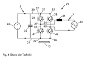
図4は、従来技術によるインバータ29の概略図を示している。インバータ29によってDC電圧をAC電圧に、またはその逆に変換することができ、電気エネルギーの流れは両方向矢印15の方向に実現し得る。このため、図中の電力コンバータの入力2と出力7の指定は任意に選択される。インバータ29は、リンク回路コンデンサ32を介して互いに接続された第1のリンク回路極30および第2のリンク回路極31を有するリンク回路28を具える。インバータ29は、第1のリンク回路極30に接続された接続点21または35と第2のリンク回路極31に接続された接続点22または36との間で延びる2つのハーフブリッジ33および34を具え、接続点21または35を起点として、それぞれがハイサイドパワー半導体スイッチ37または38、分岐点39または40、およびローサイドパワー半導体スイッチ41または42からなる直列接続を構成している。分岐点39は、出力7の方向にその下流に接続されたチョーク44を有する。DC電圧ジェネレータ45がインバータ29の入力2に接続され、AC電圧グリッド46がインバータ29の出力7に接続される。電圧を設定するために、パワー半導体スイッチを駆動してスイッチングするための駆動回路(図示せず)が、必要に応じて、両方向矢印15の両方向に電気エネルギーの流れが実現するように配置されている。
FIG. 4 shows a schematic diagram of an
図5は、本発明の第1の例示的な実施形態による昇圧コンバータ48の形態の電力コンバータの概略図を示す。第1パワー半導体スイッチ6aを駆動するために、駆動回路49がパワー半導体スイッチ6aの制御入力51に接続されている。駆動回路49は、クロックジェネレータ50と一体的に構成されている。駆動回路49に電圧を供給するために、補助回路構成52が含まれており、これは供給コンデンサ53、補助コンデンサ54、通常オフの補助半導体スイッチ55、ダイオード56、およびブートストラップダイオード57とを具える。補助半導体スイッチ55は、第1の接続点58を介して第1パワー半導体スイッチ6aの基準電位接続59に接続され、昇圧コンバータ48の主回路に組み込まれている。第1の接続点58を起点として、ダイオード56、第2の接続点60、および補助コンデンサ54の直列接続を含み、補助半導体スイッチ55と並列に配置されている。駆動回路49は、その電圧供給のために供給コンデンサ53に接続されており、この供給コンデンサ53は、第1の接続61によってブートストラップダイオード57を介して第2の接続点60に、また第2の接続62によって基準電位接続59へ電気的に接続されている。
FIG. 5 shows a schematic diagram of a power converter in the form of a
補助回路構成52は、補助半導体スイッチ55を駆動するための比較回路65として設計された駆動回路64をさらに具える。これは、2つの供給接続で補助コンデンサ54と並列に接続されている。また、逆方向のツェナーダイオード66、第8の接続点67、抵抗器68からなる直列接続が補助コンデンサ54と並列に配置され、比較回路65の非反転入力69が第8の接続点67に接続され、比較器回路65の反転入力(図示せず)が基準電位(図示せず)に接続されている。
The
昇圧コンバータ48の動作中および起動時の両方で、その必要な構成要素、例えば、駆動回路49に電力を供給する必要がある。起動時に、例えば、昇圧コンバータ48の入力2の第1の接続2aと第2の接続2bとの間に少なくともDC電圧が印加され、これは、例えばDCジェネレータ(図示せず)によって供給される。したがって、起動時には、第1パワー半導体スイッチ6aの基準電位接続59とさらなる主接続70との間にDC電圧が印加され、このDC電圧は第1パワー半導体スイッチ6aを通るリーク電流をもたらし、補助半導体スイッチ55がオフ状態のときに、補助コンデンサ54が、第1パワー半導体スイッチ6aを通る電流の流れによって充電される。補助コンデンサ54の電荷が第1の閾値を超えた場合、比較器回路65は、補助半導体スイッチ55の制御入力に制御信号を提供して補助半導体スイッチ55をオン状態とし、補助コンデンサ54が少なくとも部分的に充電されている場合に、供給コンデンサ53が、ブートストラップダイオード57を介して補助コンデンサ54によって充電される。この場合、補助コンデンサの充電量が第2の閾値を下回ると、比較回路が補助半導体スイッチ55の制御入力に制御信号を供給しなくなり、補助半導体スイッチ55が再びオフスイッチング状態に戻り、補助コンデンサが再充電されるようになる。昇圧コンバータ48の動作中、第1パワー半導体スイッチ6aに動作電流が流れ、充電プロセスを複数回繰り返すことによって、動作中に駆動回路49に電力を供給するために供給コンデンサ53に電力が供給される。起動時間を短縮するために、入力の第1の接続2aと供給コンデンサ53の第1の接続61とを電気的に接続する起動抵抗器63を任意に配置してもよい。
Both during operation and start-up of
図6は、本発明の第2の例示的な実施形態によるハーフブリッジ構成72を概略図で示している。図6に示されるハーフブリッジ構成72と、図3に示される従来技術のハーフブリッジ構成14の違いは、本質的に以下で説明する。接続点21と22との間に延びるハーフブリッジ構成72のハーフブリッジ20aは、同様に、接続点21を起点として、ハイサイドパワー半導体スイッチ23a、分岐点39、およびローサイドパワー半導体スイッチ24aからなる直列接続を含み、図示の例示的な実施形態では、2つのパワー半導体スイッチがそれぞれボディダイオードを内蔵しており、補助半導体スイッチ55がハーフブリッジ20aに内蔵されている。ローサイドパワー半導体スイッチ24aの駆動回路49に給電するために、後者は第1パワー半導体スイッチとして設計されており、ローサイドパワー半導体スイッチ24aを駆動するための駆動回路49が、補助半導体スイッチ55を具える補助回路構成52を介して電圧供給されるようになっている。補助回路構成52に関しては、図5の説明を参照されたい。ハイサイドパワー半導体スイッチ23aを駆動するために、ハーフブリッジ構成72は、その電圧供給のために供給コンデンサ74に電気的に接続された駆動回路73を有する。ハイサイドパワー半導体スイッチ23aを駆動するための駆動回路73に電圧供給するための供給コンデンサ74を充電するために、後者は、接続75によってハイサイドパワー半導体スイッチ23aの基準電位接続59に電気的に接続され、さらなる接続76によって、さらなるブートストラップダイオード77を介して補助回路構成52に含まれる供給コンデンサ53の第1の接続61に電気的に接続される。したがって、図示の例示的な実施形態では、ハイサイドパワー半導体スイッチ23aを駆動するための駆動回路73も同様に、ハーフブリッジ構成72の動作中にエネルギー効率の良い方法で電力供給することができる。
FIG. 6 schematically depicts a half-
図7は、本発明の第3の例示的な実施形態によるハーフブリッジ構成78を概略図で示している。図6の例示的な実施形態とは対照的に、ハイサイドパワー半導体スイッチ23aの駆動回路への電圧の代替供給が示されている。この目的のために、ハイサイドパワー半導体スイッチ23aおよびローサイドパワー半導体スイッチ24aの両方が、それぞれ第1パワー半導体スイッチとして設計されている。したがって、ハイサイドおよびローサイドのパワー半導体スイッチ23a、24aを駆動するための両方の駆動回路49a、49bは、別個の補助回路構成52a、52bを介して電圧供給される。したがって、この代替的な例示的実施形態は、同様に、ハーフブリッジ構成78の起動時および動作中に2つのパワー半導体スイッチを駆動するための駆動回路へのエネルギー効率のよい電圧供給を実現する。図6および図7のドライバ回路への電圧供給は、例えば、対応するように設計されたインバータブリッジを有する単相または三相インバータの場合には、複数のハーフブリッジを有するパワーエレクトロニクスデバイスに送ることもできる。
FIG. 7 schematically depicts a half-
図8は、本発明の第4の例示的な実施形態による、パワー半導体スイッチの駆動回路に電圧を供給するための方法のフローチャートを示す。この方法では、準備ステップVVSにおいて、最初に、起動のために、パワー半導体スイッチの基準電位接続とパワー半導体スイッチのさらなる主接続との間に電圧が印加される。第1の方法ステップVS1において、通常オフの補助スイッチがオフのスイッチング状態にある間に、補助コンデンサが、パワー半導体スイッチを流れる電流の少なくとも一部によって充電される。第2の方法ステップVS2において、補助コンデンサの充電電圧が第1の閾値を超えたときに補助スイッチがオン状態になり、補助コンデンサの電荷の少なくとも一部が供給コンデンサに放出されて駆動回路へ電圧を供給する。第3の方法ステップVS3において、補助コンデンサの充電電圧がより低い第2の閾値を下回ると、補助スイッチがオフスイッチング状態に戻される。VS1~VS3の3つのステップを複数回繰り返すことによって、パワー半導体スイッチの動作中に駆動回路に給電するために、供給コンデンサが給電される。 FIG. 8 shows a flowchart of a method for supplying voltage to a drive circuit of a power semiconductor switch according to a fourth exemplary embodiment of the invention. In this method, in a preparatory step VVS, a voltage is first applied for activation between the reference potential connection of the power semiconductor switch and the further main connection of the power semiconductor switch. In a first method step VS1, the auxiliary capacitor is charged by at least a portion of the current flowing through the power semiconductor switch while the normally off auxiliary switch is in the OFF switching state. In a second method step VS2, the auxiliary switch is turned on when the charging voltage of the auxiliary capacitor exceeds the first threshold, and at least a part of the charge of the auxiliary capacitor is discharged to the supply capacitor to supply the voltage to the drive circuit. supply. In a third method step VS3, the auxiliary switch is returned to the off-switching state when the charging voltage of the auxiliary capacitor falls below a second lower threshold. By repeating the three steps VS1 to VS3 multiple times, the supply capacitor is powered to power the drive circuit during operation of the power semiconductor switch.
1a パワーエレクトロニクスデバイス
1b 電力コンバータ
1、48 昇圧コンバータ
2 入力
2a、2b 接続部
3 DC電圧ジェネレータ
4 チョーク
5 ダイオード
6 パワー半導体スイッチ
6a 第1パワー半導体スイッチ
7 出力
8 矢印
9 降圧コンバータ
10 DC電圧源
11 矢印
14、72、78 ハーフブリッジ構成
15 両方向矢印
16 DC電圧源
18 DC電圧源
20、33、34、20a、20b ハーフブリッジ
21、35、58 接続点
22、36、60、67 接続点
23、37、38、23a ハイサイドパワー半導体スイッチ
24、41、42、24a ローサイドパワー半導体スイッチ
25、44 チョーク
26、56 ダイオード
27 ダイオード
28 リンク回路
29 インバータ
30 リンク回路極
31 リンク回路極
32 リンク回路コンデンサ
39、40 分岐点
45 DC電圧ジェネレータ
46 AC電圧グリッド
49、73、49a、49b 駆動回路
50 クロックジェネレータ
51 制御入力
52、52a、52b 補助回路構成
53、74 供給コンデンサ
54 補助コンデンサ
55 補助半導体スイッチ
57 ブートストラップダイオード
59 基準電位接続
61 第1の接続
62 第2の接続
63 起動抵抗
64 駆動回路
65 比較回路
66 ツェナーダイオード
68 抵抗器
69 非反転入力
70 さらなる主接続
75 接続
76 さらなる接続
77 さらなるブートストラップダイオード
VVS 準備ステップ
VS1、VS2、VS3 方法ステップ
1a Power electronics device
Claims (17)
前記補助半導体スイッチ(55、55a、55b)は、第1の接続点(58)を介して前記第1パワー半導体スイッチ(6a)の基準電位接続(59)に接続されており、
前記第1の接続点(58)を起点に、前記ダイオード(56)と、第2の接続点(60)と、前記補助コンデンサ(54)との直列接続が、前記補助半導体スイッチ(55、55a、55b)と並列に配置され、前記補助半導体スイッチ(55、55a、55b)がオフ状態にあるとき、前記補助コンデンサ(54)が前記第1パワー半導体スイッチ(6a)を通る電流によって充電され、
前記駆動回路(49、49a、49b)は、前記供給コンデンサ(53、53a、53b)に接続されて電圧供給され、
前記供給コンデンサ(53、53a、53b)は、第1の接続(61)によって前記ブートストラップダイオード(57)を介して前記第2の接続点(60)に、第2の接続(62)によって前記基準電位接続に電気的に接続され、前記補助半導体スイッチ(55、55a、55b)がオン状態にあり、前記補助コンデンサ(54)が少なくとも部分的に充電されている場合に、前記供給コンデンサ(53、53a、53b)が前記ブートストラップダイオード(57)を介して前記補助コンデンサ(54)によって充電され、
前記補助回路構成(52、52a、52b)が、前記補助コンデンサ(54)の充電電圧に基づいて、前記補助半導体スイッチ(55、55a、55b)の制御入力に前記補助半導体スイッチ(55、55a、55b)を切り替えるための制御信号を提供するように設計および構成された駆動回路(64)を具えることを特徴とするパワーエレクトロニクスデバイス。 A power electronics device (1a), in particular a power converter (1b), comprising a first power semiconductor switch (6a) and a drive circuit (49, 49a, 49b) for driving the first power semiconductor switch (6a). and an electrical auxiliary circuit configuration (52, 52a, 52b) for supplying voltage to the drive circuit (49, 49a, 49b), the auxiliary circuit configuration (52, 52a, 52b) comprising a capacitor (53, 53a, 53b), an auxiliary capacitor (54), a normally off auxiliary semiconductor switch (55, 55a, 55b), a diode (56), and a bootstrap diode (57);
said auxiliary semiconductor switch (55, 55a, 55b) is connected via a first connection point (58) to a reference potential connection (59) of said first power semiconductor switch (6a);
Starting from the first connection point (58), the diode (56), the second connection point (60), and the auxiliary capacitor (54) are connected in series to the auxiliary semiconductor switch (55, 55a). , 55b), and when the auxiliary semiconductor switch (55, 55a, 55b) is in an off state, the auxiliary capacitor (54) is charged by the current passing through the first power semiconductor switch (6a);
The drive circuit (49, 49a, 49b) is connected to the supply capacitor (53, 53a, 53b) and supplied with voltage,
The supply capacitor (53, 53a, 53b) is connected by a first connection (61) to the bootstrap diode (57) to the second connection point (60) and by a second connection (62) to the second connection point (60). said supply capacitor (53) is electrically connected to a reference potential connection, said auxiliary semiconductor switch (55, 55a, 55b) is in the on state and said auxiliary capacitor (54) is at least partially charged. , 53a, 53b) are charged by the auxiliary capacitor (54) via the bootstrap diode (57) ,
The auxiliary circuit configuration (52, 52a, 52b) connects the auxiliary semiconductor switch (55, 55a, 55a, A power electronics device characterized in that it comprises a drive circuit (64) designed and arranged to provide a control signal for switching 55b).
前記補助スイッチは、前記補助コンデンサ(54)の充電電圧に基づいてオン状態にされることを特徴とする方法。 A method of supplying voltage to a drive circuit (49) of a power semiconductor switch, wherein the drive circuit (49, 49a, 49b) is supplied with voltage by a supply capacitor (53, 53a, 53b), and the supply capacitor (53) , 53a, 53b), an auxiliary capacitor (54) is charged by the current flowing through said power semiconductor switch during the off-switching state of the normally off auxiliary switch, and said supply capacitor (53) charged by the auxiliary capacitor (54) when the auxiliary switch, which is normally off, is in the on state;
A method characterized in that the auxiliary switch is turned on based on the charging voltage of the auxiliary capacitor (54).
Applications Claiming Priority (3)
| Application Number | Priority Date | Filing Date | Title |
|---|---|---|---|
| DE102019104652.1 | 2019-02-25 | ||
| DE102019104652.1A DE102019104652B4 (en) | 2019-02-25 | 2019-02-25 | Power electronic device and method for supplying electrical voltage to a driver circuit of a power semiconductor switch |
| PCT/EP2020/052618 WO2020173667A1 (en) | 2019-02-25 | 2020-02-03 | Power electronics device and method for supplying electrical voltage to a driver circuit of a power semiconductor switch |
Publications (2)
| Publication Number | Publication Date |
|---|---|
| JP2022521419A JP2022521419A (en) | 2022-04-07 |
| JP7426397B2 true JP7426397B2 (en) | 2024-02-01 |
Family
ID=69528788
Family Applications (1)
| Application Number | Title | Priority Date | Filing Date |
|---|---|---|---|
| JP2021549505A Active JP7426397B2 (en) | 2019-02-25 | 2020-02-03 | Power electronic devices and methods for supplying voltage to drive circuits of power semiconductor switches |
Country Status (6)
| Country | Link |
|---|---|
| US (1) | US11990826B2 (en) |
| EP (1) | EP3931963B1 (en) |
| JP (1) | JP7426397B2 (en) |
| CN (1) | CN113632380B (en) |
| DE (1) | DE102019104652B4 (en) |
| WO (1) | WO2020173667A1 (en) |
Families Citing this family (1)
| Publication number | Priority date | Publication date | Assignee | Title |
|---|---|---|---|---|
| CN117458842B (en) * | 2023-12-26 | 2024-03-08 | 华羿微电子股份有限公司 | Half-bridge driving circuit |
Citations (2)
| Publication number | Priority date | Publication date | Assignee | Title |
|---|---|---|---|---|
| US20100066175A1 (en) | 2008-09-13 | 2010-03-18 | Infineon Technologies Ag | Circuit assembly for gating a power semiconductor switch |
| US20180145668A1 (en) | 2016-11-22 | 2018-05-24 | Mosway Technologies Limited | Voltage clamping circuit |
Family Cites Families (9)
| Publication number | Priority date | Publication date | Assignee | Title |
|---|---|---|---|---|
| DE202008013397U1 (en) * | 2008-10-09 | 2010-03-25 | Tridonicatco Schweiz Ag | Driver circuit for a semiconductor light source (LED) |
| CH699884B1 (en) * | 2008-11-07 | 2012-04-13 | Eth Zuerich | Drive circuit for power electronic switches. |
| KR101033933B1 (en) * | 2008-12-30 | 2011-05-11 | 서울과학기술대학교 산학협력단 | Non-Isolated Soft Switching DCCDC Converters with High Boost Ratio |
| US8558584B2 (en) * | 2010-11-30 | 2013-10-15 | Infineon Technologies Ag | System and method for bootstrapping a switch driver |
| EP2515439A1 (en) * | 2011-04-18 | 2012-10-24 | Philips Intellectual Property & Standards GmbH | Semiconductor switch with reliable blackout behavior and low control power |
| DE102012220118A1 (en) * | 2012-11-05 | 2014-05-22 | Bombardier Transportation Gmbh | Circuit arrangement and method for operating a circuit arrangement |
| US9780690B2 (en) * | 2016-01-28 | 2017-10-03 | Infineon Technologies Austria Ag | Resonant decoupled auxiliary supply for a switched-mode power supply controller |
| DE112017000186B4 (en) | 2016-02-16 | 2022-05-05 | Fuji Electric Co., Ltd. | semiconductor device |
| JP2018007403A (en) * | 2016-07-01 | 2018-01-11 | 三菱電機株式会社 | Power converter |
-
2019
- 2019-02-25 DE DE102019104652.1A patent/DE102019104652B4/en active Active
-
2020
- 2020-02-03 WO PCT/EP2020/052618 patent/WO2020173667A1/en not_active Ceased
- 2020-02-03 EP EP20704449.6A patent/EP3931963B1/en active Active
- 2020-02-03 JP JP2021549505A patent/JP7426397B2/en active Active
- 2020-02-03 CN CN202080016693.7A patent/CN113632380B/en active Active
-
2021
- 2021-08-24 US US17/410,225 patent/US11990826B2/en active Active
Patent Citations (2)
| Publication number | Priority date | Publication date | Assignee | Title |
|---|---|---|---|---|
| US20100066175A1 (en) | 2008-09-13 | 2010-03-18 | Infineon Technologies Ag | Circuit assembly for gating a power semiconductor switch |
| US20180145668A1 (en) | 2016-11-22 | 2018-05-24 | Mosway Technologies Limited | Voltage clamping circuit |
Also Published As
| Publication number | Publication date |
|---|---|
| US11990826B2 (en) | 2024-05-21 |
| DE102019104652B4 (en) | 2024-03-14 |
| WO2020173667A1 (en) | 2020-09-03 |
| JP2022521419A (en) | 2022-04-07 |
| CN113632380A (en) | 2021-11-09 |
| DE102019104652A1 (en) | 2020-08-27 |
| EP3931963A1 (en) | 2022-01-05 |
| CN113632380B (en) | 2025-11-21 |
| US20210384824A1 (en) | 2021-12-09 |
| EP3931963B1 (en) | 2022-08-17 |
Similar Documents
| Publication | Publication Date | Title |
|---|---|---|
| US8384236B2 (en) | Vehicle mounted converter | |
| US8487664B2 (en) | System and method for driving a switch | |
| US7486055B2 (en) | DC-DC converter having a diode module with a first series circuit and a second series with a flywheel diode | |
| US20120133420A1 (en) | System and Method for Bootstrapping a Switch Driver | |
| US11323031B2 (en) | Half-bridge driver circuit with a switched capacitor supply voltage for high side drive signal generation | |
| KR20030019133A (en) | Dc-dc converter | |
| CN104052296A (en) | System And Method For A Switched-mode Power Converter | |
| CN102480216B (en) | System and method for driving acascode switch | |
| JPH118910A (en) | Power supply equipment for hybrid electric vehicle | |
| KR101734210B1 (en) | Bidirectional dc-dc converter | |
| CN114097170B (en) | Power Systems | |
| JP5394975B2 (en) | Switching transistor control circuit and power converter using the same | |
| CN107615634B (en) | Power conversion device and power supply system using same | |
| US9780690B2 (en) | Resonant decoupled auxiliary supply for a switched-mode power supply controller | |
| JP7426397B2 (en) | Power electronic devices and methods for supplying voltage to drive circuits of power semiconductor switches | |
| CN114514681B (en) | DCDC Converter | |
| KR101030776B1 (en) | Step-up DC / DC Converters | |
| US12261517B2 (en) | H-bridge circuit with bootstrap capacitor gate drive charging circuit | |
| JP6668056B2 (en) | Power conversion device, power supply system using the same, and automobile | |
| US20190337474A1 (en) | In-vehicle power supply device | |
| JP6801343B2 (en) | Power converter | |
| JP6950495B2 (en) | Power converter | |
| EP2575246B1 (en) | Method for discharging a DC-link capacitor in a DC-DC converter apparatus, and corresponding DC-DC converter apparatus | |
| EP4335026A1 (en) | Power inverter and method for controlling a power inverter | |
| WO2025062210A1 (en) | Dc-to-dc converter with two cascaded buck converter |
Legal Events
| Date | Code | Title | Description |
|---|---|---|---|
| A621 | Written request for application examination |
Free format text: JAPANESE INTERMEDIATE CODE: A621 Effective date: 20221021 |
|
| A131 | Notification of reasons for refusal |
Free format text: JAPANESE INTERMEDIATE CODE: A131 Effective date: 20230905 |
|
| A521 | Request for written amendment filed |
Free format text: JAPANESE INTERMEDIATE CODE: A523 Effective date: 20231117 |
|
| TRDD | Decision of grant or rejection written | ||
| A01 | Written decision to grant a patent or to grant a registration (utility model) |
Free format text: JAPANESE INTERMEDIATE CODE: A01 Effective date: 20240109 |
|
| A61 | First payment of annual fees (during grant procedure) |
Free format text: JAPANESE INTERMEDIATE CODE: A61 Effective date: 20240122 |
|
| R150 | Certificate of patent or registration of utility model |
Ref document number: 7426397 Country of ref document: JP Free format text: JAPANESE INTERMEDIATE CODE: R150 |