WO2024122492A1 - 半導体装置 - Google Patents
半導体装置 Download PDFInfo
- Publication number
- WO2024122492A1 WO2024122492A1 PCT/JP2023/043259 JP2023043259W WO2024122492A1 WO 2024122492 A1 WO2024122492 A1 WO 2024122492A1 JP 2023043259 W JP2023043259 W JP 2023043259W WO 2024122492 A1 WO2024122492 A1 WO 2024122492A1
- Authority
- WO
- WIPO (PCT)
- Prior art keywords
- wires
- semiconductor device
- lead
- bonding
- semiconductor element
- Prior art date
- Legal status (The legal status is an assumption and is not a legal conclusion. Google has not performed a legal analysis and makes no representation as to the accuracy of the status listed.)
- Ceased
Links
Images


Classifications
-
- H—ELECTRICITY
- H10—SEMICONDUCTOR DEVICES; ELECTRIC SOLID-STATE DEVICES NOT OTHERWISE PROVIDED FOR
- H10D—INORGANIC ELECTRIC SEMICONDUCTOR DEVICES
- H10D80/00—Assemblies of multiple devices comprising at least one device covered by this subclass
- H10D80/20—Assemblies of multiple devices comprising at least one device covered by this subclass the at least one device being covered by groups H10D1/00 - H10D48/00, e.g. assemblies comprising capacitors, power FETs or Schottky diodes
- H10D80/251—FETs covered by H10D30/00, e.g. power FETs
-
- H—ELECTRICITY
- H10—SEMICONDUCTOR DEVICES; ELECTRIC SOLID-STATE DEVICES NOT OTHERWISE PROVIDED FOR
- H10W—GENERIC PACKAGES, INTERCONNECTIONS, CONNECTORS OR OTHER CONSTRUCTIONAL DETAILS OF DEVICES COVERED BY CLASS H10
- H10W70/00—Package substrates; Interposers; Redistribution layers [RDL]
- H10W70/40—Leadframes
- H10W70/456—Materials
- H10W70/457—Materials of metallic layers on leadframes
-
- H—ELECTRICITY
- H10—SEMICONDUCTOR DEVICES; ELECTRIC SOLID-STATE DEVICES NOT OTHERWISE PROVIDED FOR
- H10W—GENERIC PACKAGES, INTERCONNECTIONS, CONNECTORS OR OTHER CONSTRUCTIONAL DETAILS OF DEVICES COVERED BY CLASS H10
- H10W70/00—Package substrates; Interposers; Redistribution layers [RDL]
- H10W70/40—Leadframes
- H10W70/464—Additional interconnections in combination with leadframes
- H10W70/465—Bumps or wires
-
- H—ELECTRICITY
- H10—SEMICONDUCTOR DEVICES; ELECTRIC SOLID-STATE DEVICES NOT OTHERWISE PROVIDED FOR
- H10W—GENERIC PACKAGES, INTERCONNECTIONS, CONNECTORS OR OTHER CONSTRUCTIONAL DETAILS OF DEVICES COVERED BY CLASS H10
- H10W70/00—Package substrates; Interposers; Redistribution layers [RDL]
- H10W70/40—Leadframes
- H10W70/481—Leadframes for devices being provided for in groups H10D8/00 - H10D48/00
-
- H—ELECTRICITY
- H10—SEMICONDUCTOR DEVICES; ELECTRIC SOLID-STATE DEVICES NOT OTHERWISE PROVIDED FOR
- H10W—GENERIC PACKAGES, INTERCONNECTIONS, CONNECTORS OR OTHER CONSTRUCTIONAL DETAILS OF DEVICES COVERED BY CLASS H10
- H10W72/00—Interconnections or connectors in packages
-
- H—ELECTRICITY
- H10—SEMICONDUCTOR DEVICES; ELECTRIC SOLID-STATE DEVICES NOT OTHERWISE PROVIDED FOR
- H10W—GENERIC PACKAGES, INTERCONNECTIONS, CONNECTORS OR OTHER CONSTRUCTIONAL DETAILS OF DEVICES COVERED BY CLASS H10
- H10W72/00—Interconnections or connectors in packages
- H10W72/071—Connecting or disconnecting
-
- H—ELECTRICITY
- H10—SEMICONDUCTOR DEVICES; ELECTRIC SOLID-STATE DEVICES NOT OTHERWISE PROVIDED FOR
- H10W—GENERIC PACKAGES, INTERCONNECTIONS, CONNECTORS OR OTHER CONSTRUCTIONAL DETAILS OF DEVICES COVERED BY CLASS H10
- H10W74/00—Encapsulations, e.g. protective coatings
- H10W74/10—Encapsulations, e.g. protective coatings characterised by their shape or disposition
- H10W74/111—Encapsulations, e.g. protective coatings characterised by their shape or disposition the semiconductor body being completely enclosed
-
- H—ELECTRICITY
- H10—SEMICONDUCTOR DEVICES; ELECTRIC SOLID-STATE DEVICES NOT OTHERWISE PROVIDED FOR
- H10W—GENERIC PACKAGES, INTERCONNECTIONS, CONNECTORS OR OTHER CONSTRUCTIONAL DETAILS OF DEVICES COVERED BY CLASS H10
- H10W90/00—Package configurations
-
- H—ELECTRICITY
- H10—SEMICONDUCTOR DEVICES; ELECTRIC SOLID-STATE DEVICES NOT OTHERWISE PROVIDED FOR
- H10W—GENERIC PACKAGES, INTERCONNECTIONS, CONNECTORS OR OTHER CONSTRUCTIONAL DETAILS OF DEVICES COVERED BY CLASS H10
- H10W90/00—Package configurations
- H10W90/811—Multiple chips on leadframes
-
- H—ELECTRICITY
- H10—SEMICONDUCTOR DEVICES; ELECTRIC SOLID-STATE DEVICES NOT OTHERWISE PROVIDED FOR
- H10W—GENERIC PACKAGES, INTERCONNECTIONS, CONNECTORS OR OTHER CONSTRUCTIONAL DETAILS OF DEVICES COVERED BY CLASS H10
- H10W72/00—Interconnections or connectors in packages
- H10W72/071—Connecting or disconnecting
- H10W72/075—Connecting or disconnecting of bond wires
- H10W72/07551—Connecting or disconnecting of bond wires characterised by changes in properties of the bond wires during the connecting
- H10W72/07554—Connecting or disconnecting of bond wires characterised by changes in properties of the bond wires during the connecting changes in dispositions
-
- H—ELECTRICITY
- H10—SEMICONDUCTOR DEVICES; ELECTRIC SOLID-STATE DEVICES NOT OTHERWISE PROVIDED FOR
- H10W—GENERIC PACKAGES, INTERCONNECTIONS, CONNECTORS OR OTHER CONSTRUCTIONAL DETAILS OF DEVICES COVERED BY CLASS H10
- H10W72/00—Interconnections or connectors in packages
- H10W72/50—Bond wires
- H10W72/541—Dispositions of bond wires
- H10W72/5445—Dispositions of bond wires being orthogonal to a side surface of the chip, e.g. parallel arrangements
-
- H—ELECTRICITY
- H10—SEMICONDUCTOR DEVICES; ELECTRIC SOLID-STATE DEVICES NOT OTHERWISE PROVIDED FOR
- H10W—GENERIC PACKAGES, INTERCONNECTIONS, CONNECTORS OR OTHER CONSTRUCTIONAL DETAILS OF DEVICES COVERED BY CLASS H10
- H10W72/00—Interconnections or connectors in packages
- H10W72/50—Bond wires
- H10W72/551—Materials of bond wires
- H10W72/552—Materials of bond wires comprising metals or metalloids, e.g. silver
- H10W72/5522—Materials of bond wires comprising metals or metalloids, e.g. silver comprising gold [Au]
-
- H—ELECTRICITY
- H10—SEMICONDUCTOR DEVICES; ELECTRIC SOLID-STATE DEVICES NOT OTHERWISE PROVIDED FOR
- H10W—GENERIC PACKAGES, INTERCONNECTIONS, CONNECTORS OR OTHER CONSTRUCTIONAL DETAILS OF DEVICES COVERED BY CLASS H10
- H10W72/00—Interconnections or connectors in packages
- H10W72/50—Bond wires
- H10W72/551—Materials of bond wires
- H10W72/552—Materials of bond wires comprising metals or metalloids, e.g. silver
- H10W72/5525—Materials of bond wires comprising metals or metalloids, e.g. silver comprising copper [Cu]
-
- H—ELECTRICITY
- H10—SEMICONDUCTOR DEVICES; ELECTRIC SOLID-STATE DEVICES NOT OTHERWISE PROVIDED FOR
- H10W—GENERIC PACKAGES, INTERCONNECTIONS, CONNECTORS OR OTHER CONSTRUCTIONAL DETAILS OF DEVICES COVERED BY CLASS H10
- H10W74/00—Encapsulations, e.g. protective coatings
- H10W74/10—Encapsulations, e.g. protective coatings characterised by their shape or disposition
- H10W74/111—Encapsulations, e.g. protective coatings characterised by their shape or disposition the semiconductor body being completely enclosed
- H10W74/114—Encapsulations, e.g. protective coatings characterised by their shape or disposition the semiconductor body being completely enclosed by a substrate and the encapsulations
-
- H—ELECTRICITY
- H10—SEMICONDUCTOR DEVICES; ELECTRIC SOLID-STATE DEVICES NOT OTHERWISE PROVIDED FOR
- H10W—GENERIC PACKAGES, INTERCONNECTIONS, CONNECTORS OR OTHER CONSTRUCTIONAL DETAILS OF DEVICES COVERED BY CLASS H10
- H10W90/00—Package configurations
- H10W90/701—Package configurations characterised by the relative positions of pads or connectors relative to package parts
- H10W90/751—Package configurations characterised by the relative positions of pads or connectors relative to package parts of bond wires
- H10W90/753—Package configurations characterised by the relative positions of pads or connectors relative to package parts of bond wires between laterally-adjacent chips
-
- H—ELECTRICITY
- H10—SEMICONDUCTOR DEVICES; ELECTRIC SOLID-STATE DEVICES NOT OTHERWISE PROVIDED FOR
- H10W—GENERIC PACKAGES, INTERCONNECTIONS, CONNECTORS OR OTHER CONSTRUCTIONAL DETAILS OF DEVICES COVERED BY CLASS H10
- H10W90/00—Package configurations
- H10W90/701—Package configurations characterised by the relative positions of pads or connectors relative to package parts
- H10W90/751—Package configurations characterised by the relative positions of pads or connectors relative to package parts of bond wires
- H10W90/756—Package configurations characterised by the relative positions of pads or connectors relative to package parts of bond wires between a chip and a stacked lead frame, conducting package substrate or heat sink
Definitions
- This disclosure relates to a semiconductor device.
- Patent Document 1 discloses an example of a conventional semiconductor device.
- the semiconductor device disclosed in the document comprises a semiconductor element, multiple leads, and a sealing resin.
- One electrode and one lead of the semiconductor element are connected to each other via multiple wires.
- An object of the present disclosure is to provide a semiconductor device that is an improvement over conventional devices.
- an object of the present disclosure is to provide a semiconductor device that is capable of achieving a large current.
- an object of the present disclosure is to provide a semiconductor device that can prevent the wires and sealing resin from peeling off from the leads.
- the semiconductor device provided by the first aspect of the present disclosure comprises a first semiconductor element, a plurality of leads, a plurality of wires, and a sealing resin covering the first semiconductor element, at least a portion of each of the plurality of leads, and the plurality of wires.
- the plurality of leads includes a first lead
- the plurality of wires includes a plurality of first wires, each of which has a first bonding portion connected to the first semiconductor element and a second bonding portion connected to the first lead.
- the first lead has a first portion that extends in a first direction perpendicular to the thickness direction of the first semiconductor element.
- the second bonding portions of the plurality of first wires are connected to the first portion and form a plurality of rows along the first direction.
- the semiconductor device provided by the second aspect of the present disclosure includes a first semiconductor element, a plurality of leads, a plurality of wires, and a sealing resin covering the first semiconductor element, at least a portion of each of the plurality of leads, and the plurality of wires.
- the plurality of leads includes a first lead
- the plurality of wires includes a plurality of first wires, each of which has a first bonding portion connected to the first semiconductor element and a second bonding portion connected to the first lead.
- the first lead has a first portion extending in a first direction perpendicular to a thickness direction of the first semiconductor element.
- the second bonding portions of the plurality of first wires are connected to the first portion.
- the first lead has a first base material and a first metal layer laminated on the first base material and to which the second bonding portions of the plurality of first wires are joined.
- the first metal layer includes a plurality of first regions arranged along the first direction in the first portion.
- the above configuration allows the semiconductor device to handle a larger current. Alternatively, it can prevent the wires and sealing resin from peeling off from the leads in the semiconductor device.
- FIG. 1 is a plan view showing a semiconductor device according to a first embodiment of the present disclosure.
- FIG. 2 is a partial plan view showing the semiconductor device according to the first embodiment of the present disclosure.
- FIG. 3 is a cross-sectional view taken along line III-III in FIG.
- FIG. 4 is a cross-sectional view taken along line IV-IV in FIG.
- FIG. 5 is a cross-sectional view taken along line VV in FIG.
- FIG. 6 is a cross-sectional view taken along line VI-VI in FIG.
- FIG. 7 is a partial enlarged plan view showing the semiconductor device according to the first embodiment of the present disclosure.
- FIG. 8 is a partially enlarged cross-sectional view taken along line VIII-VIII in FIG.
- FIG. 9 is a partially enlarged cross-sectional view taken along line IX-IX of FIG.
- FIG. 10 is a partial enlarged plan view showing the semiconductor device according to the first embodiment of the present disclosure.
- FIG. 11 is a cross-sectional view taken along line XI-XI of FIG.
- FIG. 12 is a cross-sectional view taken along line XII-XII in FIG.
- FIG. 13 is a partial enlarged plan view showing the semiconductor device according to the first embodiment of the present disclosure.
- FIG. 14 is a cross-sectional view taken along line XIV-XIV in FIG.
- FIG. 15 is a cross-sectional view taken along line XV-XV in FIG.
- FIG. 16 is a partial enlarged plan view showing the semiconductor device according to the first embodiment of the present disclosure.
- FIG. 17 is a cross-sectional view taken along line XVII-XVII in FIG.
- FIG. 18 is a cross-sectional view taken along line XVIII-XVIII in FIG.
- FIG. 19 is a partial enlarged plan view showing a semiconductor device according to a second embodiment of the present disclosure.
- FIG. 20 is a partial enlarged plan view showing a semiconductor device according to a second embodiment of the present disclosure.
- FIG. 21 is a partial enlarged plan view showing a semiconductor device according to a third embodiment of the present disclosure.
- FIG. 22 is a partial enlarged plan view showing a semiconductor device according to a third embodiment of the present disclosure.
- FIG. 23 is a partial enlarged plan view showing a first modified example of the semiconductor device according to the third embodiment of the present disclosure.
- FIG. 24 is a partial enlarged plan view showing a first modified example of the semiconductor device according to the third embodiment of the present disclosure.
- FIG. 25 is a partial enlarged plan view showing a semiconductor device according to a fourth embodiment of the present disclosure.
- FIG. 26 is a partial enlarged plan view showing a semiconductor device according to a fourth embodiment of the present disclosure.
- FIG. 27 is a partial enlarged plan view showing a semiconductor device according to a fifth embodiment of the present disclosure.
- FIG. 28 is a partial enlarged plan view showing a semiconductor device according to a fifth embodiment of the present disclosure.
- FIG. 29 is a partial enlarged plan view showing a semiconductor device according to a sixth embodiment of the present disclosure.
- FIG. 30 is a partial enlarged plan view showing a semiconductor device according to a sixth embodiment of the present disclosure.
- FIG. 31 is a partial enlarged plan view showing a semiconductor device according to the seventh embodiment of the present disclosure.
- FIG. 32 is a partial enlarged plan view showing the semiconductor device according to the seventh
- an object A is formed on an object B" and “an object A is formed on an object B” include “an object A is formed directly on an object B” and “an object A is formed on an object B with another object interposed between the object A and the object B” unless otherwise specified.
- an object A is disposed on an object B” and “an object A is disposed on an object B” include “an object A is disposed directly on an object B” and “an object A is disposed on an object B with another object interposed between the object A and the object B" unless otherwise specified.
- an object A is located on an object B includes “an object A is located on an object B in contact with an object B” and “an object A is located on an object B with another object interposed between the object A and the object B” unless otherwise specified.
- an object A overlaps an object B when viewed in a certain direction includes “an object A overlaps the entire object B” and “an object A overlaps a part of an object B.”
- a surface A faces (one side or the other side of) direction B” is not limited to the case where the angle of surface A with respect to direction B is 90 degrees, but also includes the case where surface A is tilted with respect to direction B.
- First embodiment: 1 to 18 show a semiconductor device according to a first embodiment of the present disclosure.
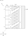
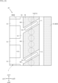
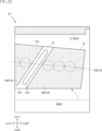
- the semiconductor device A1 of this embodiment includes a first lead 1, a second lead 2, a third lead 3, a plurality of fourth leads 41, a plurality of fifth leads 42, a plurality of sixth leads 43, a plurality of seventh leads 44, a first semiconductor element 51, a second semiconductor element 52, a plurality of first wires 71, a plurality of second wires 72, a plurality of third wires 73, a plurality of fourth wires 74, a plurality of fifth wires 75, and a sealing resin 8.
- FIG. 1 is a plan view showing the semiconductor device A1.
- FIG. 2 is a partial plan view showing the semiconductor device A1.
- FIG. 3 is a cross-sectional view taken along line III-III in FIG. 1.
- FIG. 4 is a cross-sectional view taken along line IV-IV in FIG. 1.
- FIG. 5 is a cross-sectional view taken along line V-V in FIG. 1.
- FIG. 6 is a cross-sectional view taken along line VI-VI in FIG. 1.
- FIG. 7 is a partial enlarged plan view showing the semiconductor device A1.
- FIG. 8 is a partial enlarged cross-sectional view taken along line VIII-VIII in FIG. 7.
- FIG. 9 is a partial enlarged cross-sectional view taken along line IX-IX in FIG. 7.
- FIG. 10 is a partial enlarged plan view showing the semiconductor device A1.
- FIG. 11 is a cross-sectional view taken along line XI-XI in FIG. 10.
- FIG. 12 is a cross-sectional view taken along line XII-XII in FIG. 10.
- FIG. 13 is a partial enlarged plan view showing the semiconductor device A1.
- FIG. 14 is a cross-sectional view taken along line XIV-XIV in FIG. 13.
- FIG. 15 is a cross-sectional view taken along line XV-XV in FIG. 13.
- FIG. 16 is a partially enlarged plan view showing semiconductor device A1.
- FIG. 17 is a cross-sectional view taken along line XVII-XVII in FIG. 16.
- FIG. 18 is a cross-sectional view taken along line XVIII-XVIII in FIG. 16.
- first wire 71, second wire 72, third wire 73, and fourth wire 74 are omitted in FIG. 2.
- three mutually orthogonal directions are referred to as appropriate. As an example, they are the thickness direction z, the x direction which is one direction orthogonal to the thickness direction z, and the y direction which is orthogonal to the thickness direction z and the x direction.
- the first lead 1 is a conductive member constituting a part of a conductive path to the semiconductor device A1. As shown in FIGS. 1 to 4 and 7 to 12, the first lead 1 of this embodiment has a first base material 15 and a first metal layer 16.
- the first base material 15 contains metals such as Cu (copper) and 42 alloy (iron-nickel alloy).
- the material constituting the first base material 15 is preferably a material having a higher bonding strength with the sealing resin 8 than the material constituting the first metal layer 16.
- the first metal layer 16 is formed on the first base material 15 and is a plating layer containing metals such as Ag (silver), Ni (nickel), Pd (palladium), and Au (gold).
- the material constituting the first metal layer 16 is preferably a material having a higher bonding strength with the first wire 71 and the second wire 72 than the material constituting the first base material 15.
- the first lead 1 has a first portion 11, a second portion 12, and a plurality of first terminal portions 13.
- the first portion 11 extends along the x direction.
- the x direction is an example of a "first direction”.
- the first portion 11 has a first edge 111 and a second edge 112.
- the first edge 111 is an edge on the y2 side of the first portion 11 in the y direction and extends along the x direction.
- the second edge 112 is an edge on the y1 side of the first portion 11 in the y direction and extends along the x direction.
- the first portion 11 of this embodiment also has a plurality of first recesses 115.
- the first recesses 115 are recessed toward the z2 side in the z direction.
- the multiple first recesses 115 are arranged at intervals in the x direction.
- the first recesses 115 are grooves extending in a direction intersecting the x and y directions.
- the second part 12 extends along the y direction.
- the second part 12 has a third edge 121 and a fourth edge 122.
- the third edge 121 is the edge on the x1 side of the x direction of the second part 12, and is slightly inclined with respect to the y direction.
- the fourth edge 122 is the edge on the x2 side of the x direction of the second part 12, and is aligned along the x direction.
- the first metal layer 16 includes a plurality of first regions 161 and a plurality of second regions 162.
- the plurality of first regions 161 are formed on the first portion 11 and are arranged along the x direction. Between adjacent first regions 161, there are regions where the first metal layer 16 is not formed and where the first base material 15 is exposed. In the illustrated example, the first regions 161 reach the first edge 111. Also, the first regions 161 are separated from the second edge 112.
- the second regions 162 are formed on the second part 12 and are arranged along the y direction. Between adjacent second regions 162, there are regions where the first metal layer 16 is not formed and the first base material 15 is exposed.
- the first region 161 located closest to the x2 side in the x direction and the second region 162 located closest to the y1 side in the y direction are connected to each other.
- the second region 162 reaches the third edge 121.
- the second region 162 located on the y1 side in the y direction is away from the fourth edge 122.
- the second region 162 located on the y2 side in the y direction reaches the fourth edge 122.
- the first portion 11 of this embodiment has a plurality of first recesses 115.
- the first recesses 115 are recessed toward the z2 side in the z direction.
- the plurality of first recesses 115 are arranged at intervals in the x direction.
- the first recesses 115 are disposed between adjacent first regions 161 in the x direction.
- the first recesses 115 are grooves extending in a direction intersecting the x direction and the y direction.
- the side of the first region 161 facing the first recesses 115 is parallel to the first recesses 115.
- the second portion 12 of this embodiment also has a second recess 125.
- the second recess 125 is recessed toward the z2 side in the z direction.
- the second recess 125 is disposed between adjacent second regions 162 in the y direction.
- the second recess 125 is a groove extending in a direction intersecting the x direction and the y direction.
- the side of the second region 162 facing the second recess 125 is parallel to the second recess 125.
- the multiple first terminal portions 13 extend from the first portion 11 to the y1 side in the y direction, and are arranged at the same pitch in the x direction.
- the multiple first terminal portions 13 protrude from the sealing resin 8 to the y1 side in the y direction.
- the portion of the first terminal portion 13 protruding from the sealing resin 8 has a bent shape.
- the second lead 2 is a conductive member constituting a part of the conductive path to the semiconductor device A1. As shown in FIGS. 1 to 3, 6, and 13 to 18, the second lead 2 of this embodiment is located on the y2 side in the y direction with respect to the first lead 1.
- the second lead 2 has a second base material 25 and a second metal layer 26.
- the second base material 25 contains metals such as Cu (copper) and 42 alloy (iron-nickel alloy).
- the material constituting the second base material 25 is preferably a material having a higher bonding strength with the sealing resin 8 than the material constituting the second metal layer 26.
- the second metal layer 26 is formed on the second base material 25 and is a plating layer containing metals such as Ag (silver), Ni (nickel), Pd (palladium), and Au (gold).
- the material constituting the second metal layer 26 is preferably a material having a higher bonding strength with the third wire 73 and the fourth wire 74 than the material constituting the second base material 25.
- the second lead 2 has a third portion 21 , a fourth portion 22 and a plurality of second terminal portions 23 .
- the third portion 21 extends along the x direction.
- the third portion 21 has a fifth edge 211 and a sixth edge 212.
- the fifth edge 211 is the edge on the y1 side of the third portion 21 in the y direction and is aligned along the x direction.
- the sixth edge 212 is the edge on the y2 side of the third portion 21 in the y direction and is aligned along the x direction.
- the third portion 21 of this embodiment also has a plurality of third recesses 215.
- the third recesses 215 are recessed toward the z2 side in the z direction.
- the third recesses 215 are arranged at intervals in the x direction. In the illustrated example, the third recesses 215 are grooves extending in a direction intersecting the x and y directions.
- the fourth portion 22 extends along the y direction.
- the fourth portion 22 has a seventh edge 221 and an eighth edge 222.
- the seventh edge 221 is the edge on the x1 side of the x direction of the fourth portion 22, and is slightly inclined with respect to the y direction.
- the eighth edge 222 is the edge on the x2 side of the x direction of the fourth portion 22, and is aligned along the x direction.
- the second metal layer 26 includes a plurality of third regions 261 and a plurality of fourth regions 262.
- the plurality of third regions 261 are formed on the third portion 21 and are arranged along the x direction. Between adjacent third regions 261, there are regions where the second metal layer 26 is not formed and where the second base material 25 is exposed. In the illustrated example, the third regions 261 reach the fifth edge 211. Also, the third regions 261 are separated from the sixth edge 212.
- the multiple fourth regions 262 are formed on the fourth portion 22 and are arranged along the y direction. Between adjacent fourth regions 262, there are regions where the second metal layer 26 is not formed and the second base material 25 is exposed.
- the third region 261 located closest to the x2 side in the x direction and the fourth region 262 located closest to the y2 side in the y direction are connected to each other.
- the fourth region 262 reaches the seventh edge 221.
- the fourth region 262 located on the y2 side in the y direction is away from the eighth edge 222.
- the fourth region 262 located on the y1 side in the y direction reaches the eighth edge 222.
- the third portion 21 of this embodiment has a plurality of third recesses 215.
- the third recesses 215 are recessed toward the z2 side in the z direction.
- the plurality of third recesses 215 are arranged at intervals in the x direction.
- the third recesses 215 are disposed between adjacent third regions 261 in the x direction.
- the third recesses 215 are grooves extending in a direction intersecting the x direction and the y direction.
- the side of the third region 261 facing the third recesses 215 is parallel to the third recesses 215.
- the fourth portion 22 in this embodiment has a fourth recess 225.
- the fourth recess 225 is recessed toward the z2 side in the z direction.
- the fourth recess 225 is disposed between adjacent fourth regions 262 in the y direction.
- the fourth recess 225 is a groove extending in a direction intersecting the x direction and the y direction.
- the side of the fourth region 262 facing the fourth recess 225 is parallel to the fourth recess 225.
- the second terminal portions 23 extend from the third portion 21 to the y2 side in the y direction, and are arranged at the same pitch in the x direction.
- the second terminal portions 23 protrude from the sealing resin 8 to the y2 side in the y direction.
- the portion of the second terminal portion 23 protruding from the sealing resin 8 has a bent shape.
- the third lead 3 is located between the first lead 1 and the second lead 2 in the y direction.
- the third lead 3 has a third base material 35 and a third metal layer 36.
- the third base material 35 includes a metal such as Cu (copper) or 42 alloy (iron-nickel alloy).
- the third metal layer 36 is formed on the third base material 35 and is a plating layer including a metal such as Ag (silver), Ni (nickel), Pd (palladium), or Au (gold).
- the third lead 3 has an island portion 31 and a pair of extension portions 32.
- the island portion 31 has a rectangular shape when viewed from the z direction, and is the portion on which the first semiconductor element 51 and the second semiconductor element 52 are mounted.
- the island portion 31 is exposed from the sealing resin 8 on the z2 side in the z direction.
- a pair of extension portions 32 extend from the island portion 31 on both sides in the x direction. In the illustrated example, the extension portions 32 have a bent shape when viewed from the y direction.
- a plurality of fourth leads 41 As shown in FIG. 1 and FIG. 2, the plurality of fourth leads 41 are arranged on the x1 side in the x direction with respect to the first lead 1, and on the y1 side in the y direction with respect to the island portion 31. The plurality of fourth leads 41 are arranged in the x direction.
- the fourth lead 41 has a pad portion 411 and a terminal portion 412.
- the pad portion 411 is a portion arranged on the y1 side in the y direction with respect to the island portion 31.
- the pad portion 411 may be provided with a metal layer similar to the first metal layer 16, for example.
- the terminal portion 412 extends from the pad portion 411 to the y1 side in the y direction, and protrudes from the sealing resin 8 to the y1 side in the y direction.
- the arrangement pitch of the terminal portions 412 in the x direction may be the same as the arrangement pitch of the plurality of first terminal portions 13, for example.
- the portion of the terminal portion 412 protruding from the sealing resin 8 has a bent shape similar to the first terminal portion 13.
- a plurality of fifth leads 42 As shown in FIG. 1 and FIG. 2, the plurality of fifth leads 42 are arranged on the x1 side in the x direction with respect to the second lead 2, and on the y2 side in the y direction with respect to the island portion 31. The plurality of fifth leads 42 are arranged in the x direction.
- the fifth lead 42 has a pad portion 421 and a terminal portion 422.
- the pad portion 421 is a portion arranged on the y2 side in the y direction with respect to the island portion 31.
- the pad portion 421 may be provided with a metal layer similar to the second metal layer 26, for example.
- the terminal portion 422 extends from the pad portion 421 to the y2 side in the y direction, and protrudes from the sealing resin 8 to the y2 side in the y direction.
- the arrangement pitch of the terminal portions 422 in the x direction may be the same as the arrangement pitch of the plurality of second terminal portions 23, for example.
- the portion of the terminal portion 422 protruding from the sealing resin 8 has a bent shape similar to the second terminal portion 23.
- a plurality of sixth leads 43 As shown in FIG. 1 and FIG. 2, the sixth leads 43 are arranged on the x1 side in the x direction with respect to the fourth leads 41 and the island portion 31, and are arranged on the y1 side in the y direction with respect to the extension portion 32 located on the x1 side in the x direction.
- the sixth leads 43 are arranged in the x direction.
- the sixth leads 43 have a pad portion 431 and a terminal portion 432.
- the pad portion 431 is a portion arranged on the x1 side in the x direction with respect to the island portion 31.
- the pad portion 431 may be provided with a metal layer similar to the first metal layer 16, for example.
- the terminal portion 432 extends from the pad portion 431 to the y1 side in the y direction and protrudes from the sealing resin 8 to the y1 side in the y direction.
- the arrangement pitch of the terminal portions 432 in the x direction may be the same as the arrangement pitch of the first terminal portions 13 and the terminal portions 412, for example.
- the portion of the terminal portion 432 protruding from the sealing resin 8 has a bent shape similar to the first terminal portion 13 and the terminal portion 412.
- a plurality of seventh leads 44 As shown in FIG. 1 and FIG. 2, the seventh leads 44 are arranged on the x1 side in the x direction with respect to the fifth leads 42 and the island portion 31, and are arranged on the y2 side in the y direction with respect to the extension portion 32 located on the x1 side in the x direction.
- the seventh leads 44 are arranged in the x direction.
- the seventh leads 44 have a pad portion 441 and a terminal portion 442.
- the pad portion 441 is a portion arranged on the x1 side in the x direction with respect to the island portion 31.
- the pad portion 441 may be provided with a metal layer similar to the second metal layer 26, for example.
- the terminal portion 442 extends from the pad portion 441 to the y2 side in the y direction and protrudes from the sealing resin 8 to the y2 side in the y direction.
- the arrangement pitch of the terminal portions 442 in the x direction may be the same as the arrangement pitch of the second terminal portions 23 and the terminal portions 422, for example.
- the portion of the terminal portion 442 protruding from the sealing resin 8 has a bent shape similar to the second terminal portion 23 and the terminal portion 422.
- the first semiconductor element 51 is an element that performs the main electrical function of the semiconductor device A1.
- the type of the first semiconductor element 51 is not limited in any way, and in this embodiment, the first semiconductor element 51 is a switching element, for example, a Si-MOSFET (Metal-Oxide-Semiconductor Field-Effect Transistor).
- the first semiconductor element 51 has a first electrode 511 and a plurality of second electrodes 512.
- the first electrode 511 is, for example, a source electrode.
- the plurality of second electrodes 512 include, for example, a gate electrode and a source sense electrode.
- the first semiconductor element 51 also has a drain electrode (not shown) disposed on the z2 side in the z direction. This drain electrode is conductively joined to the island portion 31 (third metal layer 36), so that the first semiconductor element 51 is mounted on the island portion 31.
- the first electrode 511 may be an electrode of an integrated structure that occupies most of the first semiconductor element 51 when viewed from the z direction, or may be composed of multiple electrodes that are discretely arranged when viewed from the z direction.
- Distributed electrodes refer to electrodes that are intentionally arranged so as not to cause a large bias in a certain area, such as in a matrix shape.
- Figure 2 shows an example in which multiple first electrodes 511 are discretely arranged.
- the multiple second electrodes 512 are arranged on the x1 side in the x direction relative to the first electrode 511.
- the multiple second electrodes 512 are arranged in the y direction.
- the second semiconductor element 52 has a function as, for example, a gate driver IC that controls the first semiconductor element 51.
- the second semiconductor element 52 is mounted on the island portion 31, and is disposed on the x1 side in the x direction with respect to the first semiconductor element 51.
- the first semiconductor element 51 has an elongated rectangular shape when viewed from the z direction, and is smaller than the first semiconductor element 51.
- the second semiconductor element 52 has a plurality of electrodes 521, a plurality of electrodes 522, and a plurality of electrodes 523.
- a plurality of first wires 71 are connected to the first electrodes 511 of the first semiconductor element 51 and the first portions 11 of the first leads 1.
- the specific configuration of the first wires 71 is not limited in any way, and may be, for example, a configuration in which a core material containing Cu (copper) is coated with Pd (palladium).
- Other examples of the core material of the first wires 71 include Au (gold) and Ag (silver).
- the first wire 71 has a first bonding portion 711 and a second bonding portion 712.
- the first bonding portion 711 is a block-shaped portion.
- the second bonding portion 712 is a flat portion that is expanded by the capillary Cp toward the connection target.
- the first bonding portions 711 of the multiple first wires 71 are individually connected to multiple first electrodes 511.
- the second bonding portions 712 are connected to multiple first regions 161 of the first metal layer 16.
- the second bonding parts 712 are arranged in multiple rows along the x direction.
- the first wires 71 are omitted, and the parts where the second bonding parts 712 can be formed are shown by circular imaginary lines. These imaginary lines may remain as traces of the capillary Cp being pressed.
- the second bonding parts 712 are arranged in two rows.
- the second bonding parts 712 are arranged in a staggered pattern.
- the arrangement pitch of the second bonding parts 712 in the x direction is, for example, about 206 ⁇ m.
- the pitch of the second bonding parts 712 included in different rows and diagonally adjacent in the figure is also about 206 ⁇ m.
- the three adjacent second bonding parts 712 are arranged at positions corresponding to the corners of an equilateral triangle.
- the direction in which the first recess 115 extends coincides (or approximately coincides) with the direction in which the adjacent first wire 71 extends when viewed from the z direction.
- a plurality of second wires 72 are connected to the first electrode 511 of the first semiconductor element 51 and the second portion 12 of the first lead 1.
- the specific configuration of the second wires 72 is not limited in any way, and may be, for example, a configuration in which a core material containing Cu (copper) is coated with Pd (palladium).
- Other examples of the core material of the second wires 72 include Au (gold) and Ag (silver).
- the second wire 72 has a first bonding portion 721 and a second bonding portion 722.
- the first bonding portion 721 is a block-shaped portion.
- the second bonding portion 722 is a flat portion that is expanded by the capillary Cp toward the connection target.
- the first bonding portions 721 of the multiple second wires 72 are individually connected to multiple first electrodes 511.
- the second bonding portions 722 are connected to multiple second regions 162 of the first metal layer 16.
- the second bonding portions 722 are arranged in multiple rows along a direction slightly tilted with respect to the y direction. This slightly tilted direction is an example of the "second direction".
- the second wires 72 are omitted, and the portion where the second bonding portion 722 can be formed is shown by a circular imaginary line. This imaginary line may remain as a trace of, for example, the capillary Cp being pressed.
- the second bonding portions 722 are arranged in three rows. Also, the second bonding portions 722 are arranged in a staggered pattern.
- the arrangement pitch of the second bonding portions 722 in the x direction is, for example, about 206 ⁇ m.
- the pitch of the second bonding portions 722 included in different rows and diagonally adjacent in the figure is similarly about 206 ⁇ m. That is, the three adjacent second bonding portions 722 are positioned at positions that correspond to the corners of an equilateral triangle.
- the direction in which the second recess 125 extends coincides (or approximately coincides) with the direction in which the adjacent second wire 72 extends when viewed from the z direction.
- the third wires 73 are connected to the first electrode 511 of the first semiconductor element 51 and the third portion 21 of the second lead 2.
- the specific configuration of the third wires 73 is not limited in any way, and may be, for example, a configuration in which a core material containing Cu (copper) is coated with Pd (palladium).
- Other examples of the core material of the third wires 73 include Au (gold) and Ag (silver).
- the third wire 73 has a first bonding portion 731 and a second bonding portion 732.
- the first bonding portion 731 is a block-shaped portion.
- the second bonding portion 732 is a flat portion that is expanded by the capillary Cp toward the connection target.
- the first bonding portions 731 of the multiple third wires 73 are individually connected to multiple first electrodes 511.
- the second bonding portions 732 are connected to multiple third regions 261 of the second metal layer 26.
- the second bonding parts 732 are arranged in multiple rows along the x direction.
- the third wires 73 are omitted, and the parts where the second bonding parts 732 can be formed are shown by circular imaginary lines. These imaginary lines may remain as traces of the capillary Cp being pressed against them.
- the second bonding parts 732 are arranged in two rows.
- the second bonding parts 732 are arranged in a staggered pattern.
- the wire diameter of the third wire 73 is 50 ⁇ m
- the arrangement pitch of the second bonding parts 732 in the x direction is, for example, about 206 ⁇ m.
- the pitch of the second bonding parts 732 included in different rows and diagonally adjacent in the figure is also about 206 ⁇ m.
- the three adjacent second bonding parts 732 are arranged at positions corresponding to the corners of an equilateral triangle.
- the direction in which the third recess 215 extends coincides (or approximately coincides) with the direction in which the adjacent third wire 73 extends when viewed from the z direction.
- a plurality of fourth wires 74 are connected to the first electrode 511 of the first semiconductor element 51 and the fourth portion 22 of the second lead 2.
- the specific configuration of the fourth wires 74 is not limited in any way, and an example of the fourth wires 74 is a configuration in which a core material containing Cu (copper) is coated with Pd (palladium).
- Other examples of the core material of the fourth wires 74 include Au (gold) and Ag (silver).
- the fourth wire 74 has a first bonding portion 741 and a second bonding portion 742.
- the first bonding portion 741 is a block-shaped portion.
- the second bonding portion 742 is a flat portion that is expanded by the capillary Cp toward the connection target.
- the first bonding portions 741 of the multiple fourth wires 74 are individually connected to multiple first electrodes 511.
- the second bonding portions 742 are connected to multiple fourth regions 262 of the second metal layer 26.
- the second bonding portions 742 are arranged in multiple rows along a direction slightly tilted with respect to the y direction. This slightly tilted direction is an example of the "third direction".
- the fourth wires 74 are omitted, and the portion where the second bonding portion 742 can be formed is shown by a circular imaginary line. This imaginary line may remain as a trace of, for example, the capillary Cp being pressed.
- the second bonding portions 742 are arranged in three rows. Also, the second bonding portions 742 are arranged in a staggered pattern.
- the arrangement pitch of the second bonding portions 742 in the x direction is, for example, about 206 ⁇ m.
- the pitch of the second bonding portions 742 included in different rows and diagonally adjacent in the figure is similarly about 206 ⁇ m. That is, the three adjacent second bonding parts 742 are positioned at positions that correspond to the corners of an equilateral triangle.
- the direction in which the fourth recess 225 extends coincides (or approximately coincides) with the direction in which the adjacent fourth wire 74 extends when viewed from the z direction.
- the first wire 71, the second wire 72, the third wire 73, and the fourth wire 74 are shown overlapping each other, and are prevented from interfering with each other by, for example, making the heights in the z direction different.
- the first wire 71, the second wire 72, the third wire 73, and the fourth wire 74 are all connected to the first electrode 511, so that even if any of them are in contact, the electrical function of the semiconductor device A1 can be performed.
- the fifth wires 75 include, for example, Au (gold), Cu (copper), or the like.
- a plurality of sixth wires 76 1, 2 and 4, the sixth wires 76 are individually connected to the electrodes 522 of the second semiconductor element 52 and the pad portions 411 of the fourth leads 41.
- the fifth wires 75 include, for example, Au (gold), Cu (copper), or the like.
- a plurality of seventh wires 77 1, 2 and 4, the multiple seventh wires 77 are individually connected to the multiple electrodes 523 of the second semiconductor element 52, the pad portions 431 of the multiple sixth leads 43, and the fourth lead 41 of the seventh lead 44.
- the seventh wires 77 include, for example, Au (gold), Cu (copper), or the like.
- Sealing resin 8 covers a portion of each of the first lead 1, the second lead 2, the third lead 3, the plurality of fourth leads 41, the plurality of fifth leads 42, the plurality of sixth leads 43, and the plurality of seventh leads 44, as well as the first semiconductor element 51, the second semiconductor element 52, the plurality of first wires 71, the plurality of second wires 72, the plurality of third wires 73, the plurality of fourth wires 74, and the plurality of fifth wires 75.
- the material of the sealing resin 8 is formed of, for example, a black epoxy resin.
- the sealing resin 8 has a first resin surface 81, a second resin surface 82, a third resin surface 83, a fourth resin surface 84, a fifth resin surface 85 and a sixth resin surface 86.
- the first resin surface 81 faces the z1 side in the z direction, and in the illustrated example, is a flat surface.
- the third resin surface 83 faces the z2 side in the z direction, and in the illustrated example, is a flat surface.
- the third resin surface 83 is a surface facing the x1 side in the x direction, and in the illustrated example, is curved.
- the fourth resin surface 84 is a surface facing the x2 side in the x direction, and in the illustrated example, is curved.
- the fifth resin surface 85 is a surface facing the y1 side in the y direction, and in the illustrated example, is curved.
- a plurality of first terminal portions 13, a plurality of terminal portions 412, and a plurality of terminal portions 432 protrude from the fifth resin surface 85.
- the sixth resin surface 86 is a surface facing the y2 side in the y direction, and in the illustrated example, is curved.
- a plurality of second terminal portions 23, a plurality of terminal portions 422, and a plurality of terminal portions 442 protrude from the sixth resin surface 86.
- multiple second bonding portions 712 are arranged in multiple rows. This makes it possible to increase the number of first wires 71 that can be connected to the first portion 11 of the first lead 1 of the same size. This makes it possible to increase the current capacity of the semiconductor device A1.
- the first wires 71 are arranged in a staggered pattern. This is suitable for increasing the number of the first wires 71.
- multiple second bonding portions 722 are arranged in multiple rows. This makes it possible to increase the number of second wires 72 that can be connected to the second portion 12 of the first lead 1 of the same size. This makes it possible to increase the current capacity of the semiconductor device A1.
- the second wires 72 are arranged in a staggered pattern. This is suitable for increasing the number of the second wires 72.
- the second wires 72 are also arranged in three rows. This allows the number of the second wires 72 to be further increased.
- multiple second bonding portions 732 are arranged in multiple rows. This makes it possible to increase the number of third wires 73 that can be connected to the third portion 21 of the second lead 2 of the same size. This can further promote the increase in current of the semiconductor device A1.
- the multiple third wires 73 are arranged in a staggered pattern. This is suitable for increasing the number of multiple third wires 73.
- multiple second bonding portions 742 are arranged in multiple rows. This makes it possible to increase the number of fourth wires 74 that can be connected to the fourth portion 22 of the second lead 2 of the same size. This further promotes a larger current for the semiconductor device A1.
- the multiple fourth wires 74 are arranged in a staggered pattern. This is suitable for increasing the number of multiple fourth wires 74.
- the multiple fourth wires 74 are arranged in three rows. This allows the number of multiple fourth wires 74 to be further increased.
- the multiple first bonding portions 711, the multiple first bonding portions 721, the multiple first bonding portions 731, and the multiple first bonding portions 741 are discretely arranged in a matrix shape or the like when viewed in the z direction. This makes it possible to arrange the multiple first bonding portions 711, the multiple first bonding portions 721, the multiple first bonding portions 731, and the multiple first bonding portions 741 more uniformly and without bias on the first semiconductor element 51, which is preferable for increasing the current of the semiconductor device A1.
- the multiple second bonding portions 712 are connected to the first region 161. This can increase the bonding strength between the multiple first wires 71 and the first lead 1. Furthermore, between adjacent first regions 161, there is a region where the first metal layer 16 is not provided and the first base material 15 is exposed. The presence of this region can increase the bonding strength between the first lead 1 and the sealing resin 8. Therefore, it is possible to prevent the first wires 71 and the sealing resin 8 from peeling off from the first lead 1.
- the multiple second bonding portions 722 are connected to the second region 162. This can increase the bonding strength between the multiple second wires 72 and the first lead 1. Furthermore, between adjacent second regions 162, there is a region where the first metal layer 16 is not provided and the first base material 15 is exposed. The presence of this region can increase the bonding strength between the first lead 1 and the sealing resin 8. Therefore, it is possible to prevent the second wires 72 and the sealing resin 8 from peeling off from the first lead 1.
- the multiple second bonding portions 732 are connected to the third region 261. This can increase the bonding strength between the multiple third wires 73 and the second lead 2. Furthermore, between adjacent third regions 261, there is a region where the second metal layer 26 is not provided and the second base material 25 is exposed. The presence of this region can increase the bonding strength between the second lead 2 and the sealing resin 8. This can prevent the third wires 73 and the sealing resin 8 from peeling off from the second lead 2.
- the multiple second bonding portions 742 are connected to the fourth region 262. This can increase the bonding strength between the multiple fourth wires 74 and the second lead 2. Furthermore, between adjacent fourth regions 262, there is a region where the second metal layer 26 is not provided and the second base material 25 is exposed. The presence of this region can increase the bonding strength between the second lead 2 and the sealing resin 8. This can prevent the fourth wires 74 and the sealing resin 8 from peeling off from the second lead 2.
- a first recess 115 is provided between adjacent first regions 161. This can further increase the bonding strength between the first lead 1 and the sealing resin 8. Also, the fact that the first recess 115 is a groove is suitable for placing a first recess 115 with a larger area between adjacent first regions 161. These effects are similar for the third recess 215 in the second lead 2.
- a second recess 125 is provided between adjacent second regions 162. This can further increase the bonding strength between the first lead 1 and the sealing resin 8. Also, the fact that the second recess 125 is a groove is suitable for placing a second recess 125 with a larger area between adjacent second regions 162. These effects are similar for the fourth recess 225 in the second lead 2.
- the first region 161 reaches the first edge 111.
- the first region 161 is away from the second edge 112.
- an area where the first base material 15 is exposed is located on the y1 side of the first region 161 in the y direction. This increases the bonding strength between the first lead 1 and the sealing resin 8.
- the same effect is achieved for the relationship between the third region 261 and the fifth edge 211 and the sixth edge 212 in the second lead 2.
- the second region 162 reaches the third edge 121. This allows the second bonding portion 722 to be positioned closer to the island portion 31, which is advantageous for shortening the length of the second wire 72.
- the second region 162 is away from the fourth edge 122. As a result, an area where the first base material 15 is exposed is positioned on the x2 side of the second region 162 in the x direction. This makes it possible to increase the bonding strength between the first lead 1 and the sealing resin 8. The same effect is achieved for the relationship between the fourth region 262 and the seventh edge 221 and the eighth edge 222 of the second lead 2.
- FIGS. 19 to 28 show other embodiments of the present disclosure.
- elements that are the same as or similar to those in the above embodiment are given the same reference numerals as in the above embodiment.
- the configurations of each part in each modified example and each embodiment can be combined with each other as appropriate to the extent that no technical contradictions arise.
- Second embodiment: 19 and 20 show a semiconductor device according to a second embodiment of the present disclosure.
- the first recess 115 described above is not formed in the first portion 11.
- the second recess 125 described above is not formed in the second portion 12.
- the third recess 215 may not be formed in the third portion 21, and the fourth recess 225 may not be formed in the fourth portion 22.
- This embodiment also allows the semiconductor device A2 to have a large current. It also prevents the first wire 71, the second wire 72, the third wire 73, and the fourth wire 74 from peeling off from the sealing resin 8 and the first lead 1 and the second lead 2. As can be seen from this embodiment, the first recess 115, the second recess 125, the third recess 215, and the fourth recess 225 may or may not be formed as appropriate.
- Third embodiment 21 and 22 show a semiconductor device according to a third embodiment of the present disclosure.
- the configuration of a first metal layer 16 is different from that of the above-described embodiments.
- the first metal layer 16 of this embodiment has a plurality of first connection regions 163.
- the first connection regions 163 connect adjacent first regions 161.
- two first connection regions 163 are arranged on both sides of the first recess 115 in the y direction.
- the first connection regions 163 connect the y1 side ends or the y2 side ends of adjacent first regions 161 in the y direction.
- the first metal layer 16 of this embodiment has a plurality of second connection regions 164.
- the second connection regions 164 connect adjacent second regions 162.
- two second connection regions 164 are arranged on both sides of the second recess 125 in the x direction.
- the second connection regions 164 connect the x1 side ends or the x2 side ends of adjacent second regions 162 in the x direction.
- This embodiment also allows the semiconductor device A3 to have a large current.
- the first wire 71, the second wire 72, the third wire 73, and the fourth wire 74 and the sealing resin 8 can be prevented from peeling off from the first lead 1 and the second lead 2.
- the configuration in which a plurality of first regions 161 are arranged in the x direction may be partially connected by the first connecting region 163. If the first metal layer 16 is not provided between adjacent first regions 161 and a region in which the first base material 15 is exposed is provided, an effect of preventing the sealing resin 8 from peeling off from the first lead 1 can be expected.
- the configuration in which a plurality of second regions 162 are arranged in the second direction may be partially connected by the second connecting region 164.
- first metal layer 16 is not provided between adjacent second regions 162 and a region in which the first base material 15 is exposed is provided, an effect of preventing the sealing resin 8 from peeling off from the first lead 1 can be expected. These points also apply to the third region 261 and the fourth region 262.
- first modification: 23 and 24 show a first modified example of the semiconductor device A3.
- adjacent first regions 161 are connected by one first connection region 163.
- the first connection region 163 is connected to the center (or approximately the center) of the first region 161 in the y direction.
- the first recess 115 is not formed in the first part 11.
- adjacent second regions 162 are connected by one second connection region 164.
- the second connection region 164 is connected to the center (or approximately the center) of the first region 161 in the x direction.
- the second recess 125 is not formed in the second part 12.
- This modified example also allows the semiconductor device A31 to have a large current. It also prevents the first wire 71, the second wire 72, the third wire 73, and the fourth wire 74 from peeling off from the sealing resin 8 and the first lead 1 and the second lead 2. As can be seen from this modified example, the number and arrangement of the first connecting regions 163 and the second connecting regions 164 are not limited in any way.
- Fourth embodiment: 25 and 26 show a semiconductor device according to a fourth embodiment of the present disclosure.
- the first region 161 is configured as one region extending in the x direction.
- the first recess 115 is not formed in the first part 11.
- the second region 162 is configured as one region extending in the y direction.
- the second recess 125 is not formed in the second part 12.
- This embodiment also allows the semiconductor device A4 to have a large current.
- Fifth embodiment: 27 and 28 show a semiconductor device according to a fifth embodiment of the present disclosure.
- the first lead 1 is not provided with a first metal layer 16.
- the second bonding portion 712 and the second bonding portion 722 are bonded to the first base material 15.
- the material constituting the first wire 71 and the second wire 72 and the material of the first base material 15 are a combination that can increase the bonding strength.
- This embodiment also allows the semiconductor device A5 to have a large current. As can be seen from this modified example, there is no limitation on whether the first metal layer 16 or the second metal layer 26 is present or not.
- the semiconductor device according to the present disclosure is not limited to the above-mentioned embodiment.
- the specific configuration of each part of the semiconductor device according to the present disclosure can be freely designed in various ways.
- FIG. 29 and 30 show a semiconductor device according to the sixth embodiment of the present disclosure.
- a plurality of first recesses 115 are arranged between adjacent first regions 161.
- the plurality of first recesses 115 are arranged parallel (or approximately parallel) to the opposing sides of the first regions 161.
- the shape of the first recesses 115 as viewed from the z direction is, for example, circular.
- a plurality of second recesses 125 are arranged between adjacent second regions 162.
- the plurality of second recesses 125 are arranged parallel (or approximately parallel) to the opposing sides of the second regions 162.
- the shape of the second recesses 125 as viewed from the z direction is, for example, circular.
- This embodiment also allows the semiconductor device A6 to have a large current. It also prevents the first wire 71, the second wire 72, the third wire 73, and the fourth wire 74 from peeling off from the sealing resin 8 and the first lead 1 and the second lead 2.
- the number, size, shape, arrangement, etc. of the first recesses 115 and the second recesses 125 are not limited in any way.
- Seventh embodiment 31 and 32 show a semiconductor device according to a seventh embodiment of the present disclosure.
- a plurality of second bonding parts 722 are arranged in a row as shown in Fig. 31. Also, as shown in Fig. 32, a plurality of second bonding parts 722 are arranged in a row.
- This embodiment also makes it possible to prevent the first wire 71, the second wire 72, the third wire 73, and the fourth wire 74 from peeling off from the sealing resin 8 from the first lead 1 and the second lead 2.
- the arrangement of the multiple second bonding portions 722 and the multiple second bonding portions 722 is not limited in any way. This disclosure includes the embodiments described in the following appendix.
- Appendix 1A A first semiconductor element; Multiple leads and A plurality of wires; a sealing resin covering the first semiconductor element, at least a portion of the plurality of leads, and the plurality of wires; the plurality of leads includes a first lead; the plurality of wires include a plurality of first wires each having a first bonding portion connected to the first semiconductor element and a second bonding portion connected to the first lead; the first lead has a first portion extending in a first direction perpendicular to a thickness direction of the first semiconductor element; The second bonding portions of the plurality of first wires are connected to the first portion and are arranged in a plurality of rows along the first direction.
- Appendix 2A. 1C Appendix 2A. 1C.
- the semiconductor device wherein the second bonding portions of the plurality of first wires are arranged in a staggered manner.
- the plurality of wires include a plurality of second wires each having a first bonding portion connected to the first semiconductor element and a second bonding portion connected to the first lead; the first lead has a second portion extending in a second direction intersecting the first direction when viewed in the thickness direction,
- the semiconductor device according to claim 1A or 2A, wherein the second bonding portions of the plurality of second wires are connected to the second portion and form a plurality of rows along the second direction.
- the plurality of leads includes a second lead disposed on an opposite side of the first lead across the first semiconductor element, the plurality of wires include a plurality of third wires each having a first bonding portion connected to the first semiconductor element and a second bonding portion connected to the second lead; the second lead has a third portion extending in the first direction;
- the semiconductor device according to any one of appendices 1A to 5A, wherein the second bonding portions of the multiple third wires are connected to the third portion and form multiple rows along the first direction. Appendix 7A.
- the plurality of wires include a plurality of fourth wires each having a first bonding portion connected to the first semiconductor element and a second bonding portion connected to the second lead; the second lead has a fourth portion extending in a third direction intersecting the first direction when viewed in the thickness direction,
- the semiconductor device according to claim 6A wherein the second bonding portions of the multiple fourth wires are connected to the fourth portion and form multiple rows along the third direction.
- Appendix 8A The semiconductor device according to claim 7A, wherein the second lead has a plurality of second terminal portions extending in a direction away from the first semiconductor element and protruding from the sealing resin.
- Appendix 9A Appendix 9A.
- Appendix 10A The semiconductor device according to claim 9A, wherein the first bonding portions of the plurality of first to fourth wires are discretely arranged when viewed in the thickness direction.
- Appendix 11A The semiconductor device according to claim 9A or 10A, wherein the first semiconductor element is a switching element.
- Appendix 12A The semiconductor device according to any one of claims 1A to 11A, wherein the plurality of leads includes a third lead on which the first semiconductor element is mounted.
- Appendix 13A The semiconductor device according to claim 7A or 8A, wherein the first semiconductor element has a first electrode to which the first bonding portions of the plurality of first to fourth wires are connected.
- Appendix 10A The semiconductor device according to claim 9A, wherein the first bonding portions of the plurality of first to fourth wires are discretely arranged when
- the semiconductor device of claim 12A further comprising a second semiconductor element mounted on the third lead and electrically connected to the first semiconductor element.
- Appendix 14A A semiconductor device described in any one of Appendixes 1A to 13A, wherein the first lead has a first base material and a first metal layer laminated on the first base material and to which the second bonding portions of the multiple first wires are joined.
- Appendix 15A The semiconductor device of claim 14A, wherein the first metal layer includes a plurality of first regions arranged along the first direction in the first portion.
- Appendix 16A The semiconductor device of claim 15A, wherein the first base material has a first recess located between adjacent first regions.
- Appendix 17A. 16B The semiconductor device according to claim 16A, wherein the first recess is a groove extending in a direction intersecting the first direction.
- Appendix 1B A first semiconductor element; Multiple leads and A plurality of wires; a sealing resin covering the first semiconductor element, at least a portion of the plurality of leads, and the plurality of wires;
- the plurality of leads includes a first lead;
- the plurality of wires include a plurality of first wires each having a first bonding portion connected to the first semiconductor element and a second bonding portion connected to the first lead;
- the first lead has a first portion extending in a first direction perpendicular to a thickness direction of the first semiconductor element; the second bonding portions of the first wires are connected to the first portions;
- the first lead has a first base material and a first metal layer laminated on the first base material and to which the second bonding portions of the plurality of first wires are joined;
- the first metal layer includes a plurality of first regions arranged along the first direction in the first portion.
- Appendix 2B The semiconductor device of claim 1B, wherein the first lead has a base material including Cu. Appendix 3B. 2C.
- Appendix 6B. the first portion has a first edge close to the first semiconductor element and a second edge remote from the first semiconductor element; 5C.
- the plurality of wires include a plurality of second wires each having a first bonding portion connected to the first semiconductor element and a second bonding portion connected to the first lead; the first lead has a second portion extending in a second direction intersecting the first direction when viewed in the thickness direction, the second bonding portions of the second wires are connected to the second portion; 1B.
- the first metal layer includes a plurality of second regions to which the second bonding portions of the plurality of second wires are connected and which are arranged along the second direction in the second portion.
- Appendix 11B. 10C The semiconductor device of claim 10B, wherein the second regions are spaced apart from one another.
- the semiconductor device of claim 10B wherein the first metal layer includes a second coupling region that couples adjacent second regions.
- Appendix 13B. the second portion has a third edge closer to the first semiconductor element and a fourth edge farther from the first semiconductor element; 13.
- Appendix 14B. The semiconductor device according to any one of appendices 10B to 13B, wherein the first base material has a second recess located between adjacent second regions.
- Appendix 15B The semiconductor device according to claim 14B, wherein the second recess is a groove extending in a direction intersecting the second direction.
Landscapes
- Lead Frames For Integrated Circuits (AREA)
Priority Applications (2)
| Application Number | Priority Date | Filing Date | Title |
|---|---|---|---|
| JP2024562758A JPWO2024122492A1 (https=) | 2022-12-05 | 2023-12-04 | |
| US19/222,294 US20250293199A1 (en) | 2022-12-05 | 2025-05-29 | Semiconductor device |
Applications Claiming Priority (4)
| Application Number | Priority Date | Filing Date | Title |
|---|---|---|---|
| JP2022194190 | 2022-12-05 | ||
| JP2022-194190 | 2022-12-05 | ||
| JP2022-194191 | 2022-12-05 | ||
| JP2022194191 | 2022-12-05 |
Related Child Applications (1)
| Application Number | Title | Priority Date | Filing Date |
|---|---|---|---|
| US19/222,294 Continuation US20250293199A1 (en) | 2022-12-05 | 2025-05-29 | Semiconductor device |
Publications (1)
| Publication Number | Publication Date |
|---|---|
| WO2024122492A1 true WO2024122492A1 (ja) | 2024-06-13 |
Family
ID=91379307
Family Applications (1)
| Application Number | Title | Priority Date | Filing Date |
|---|---|---|---|
| PCT/JP2023/043259 Ceased WO2024122492A1 (ja) | 2022-12-05 | 2023-12-04 | 半導体装置 |
Country Status (3)
| Country | Link |
|---|---|
| US (1) | US20250293199A1 (https=) |
| JP (1) | JPWO2024122492A1 (https=) |
| WO (1) | WO2024122492A1 (https=) |
Citations (4)
| Publication number | Priority date | Publication date | Assignee | Title |
|---|---|---|---|---|
| JP2010283053A (ja) * | 2009-06-03 | 2010-12-16 | Renesas Electronics Corp | 半導体装置及びその製造方法 |
| JP2015079789A (ja) * | 2013-10-15 | 2015-04-23 | 株式会社デンソー | 半導体装置 |
| JP2017201675A (ja) * | 2016-05-02 | 2017-11-09 | ローム株式会社 | 半導体装置および半導体装置の製造方法 |
| WO2022176729A1 (ja) * | 2021-02-22 | 2022-08-25 | ローム株式会社 | 半導体装置 |
-
2023
- 2023-12-04 WO PCT/JP2023/043259 patent/WO2024122492A1/ja not_active Ceased
- 2023-12-04 JP JP2024562758A patent/JPWO2024122492A1/ja active Pending
-
2025
- 2025-05-29 US US19/222,294 patent/US20250293199A1/en active Pending
Patent Citations (4)
| Publication number | Priority date | Publication date | Assignee | Title |
|---|---|---|---|---|
| JP2010283053A (ja) * | 2009-06-03 | 2010-12-16 | Renesas Electronics Corp | 半導体装置及びその製造方法 |
| JP2015079789A (ja) * | 2013-10-15 | 2015-04-23 | 株式会社デンソー | 半導体装置 |
| JP2017201675A (ja) * | 2016-05-02 | 2017-11-09 | ローム株式会社 | 半導体装置および半導体装置の製造方法 |
| WO2022176729A1 (ja) * | 2021-02-22 | 2022-08-25 | ローム株式会社 | 半導体装置 |
Also Published As
| Publication number | Publication date |
|---|---|
| US20250293199A1 (en) | 2025-09-18 |
| JPWO2024122492A1 (https=) | 2024-06-13 |
Similar Documents
| Publication | Publication Date | Title |
|---|---|---|
| JP7441287B2 (ja) | 半導体装置 | |
| CN100517680C (zh) | 布线基板、半导体装置及显示模块 | |
| US7839003B2 (en) | Semiconductor device including a coupling conductor having a concave and convex | |
| US20030121698A1 (en) | Semiconductor device and printed wiring board having electrode pads | |
| JP2009071156A (ja) | 半導体装置及びその製造方法 | |
| US8354744B2 (en) | Stacked semiconductor package having reduced height | |
| JP3660663B2 (ja) | チップパッケージの製造方法 | |
| WO2024122492A1 (ja) | 半導体装置 | |
| CN102034915A (zh) | 半导体发光装置 | |
| TW201001644A (en) | Semiconductor module and method of producing the same | |
| US20240258186A1 (en) | Semiconductor device | |
| KR20040032039A (ko) | 반도체장치 | |
| JP7035121B2 (ja) | 半導体装置 | |
| CN101552253B (zh) | 阵列封装基板 | |
| JP2006032871A (ja) | 半導体装置 | |
| US20250253211A1 (en) | Semiconductor device | |
| US20240421048A1 (en) | Semiconductor device | |
| US9293399B2 (en) | Semiconductor device and electronic unit provided with the same | |
| WO2024157758A1 (ja) | 半導体装置 | |
| US20250266331A1 (en) | Semiconductor device | |
| JP3964319B2 (ja) | 半導体装置 | |
| WO2025126889A1 (ja) | 半導体装置 | |
| CN118355490A (zh) | 半导体装置 | |
| WO2024161996A1 (ja) | 半導体装置 | |
| KR20040047532A (ko) | 외부전극 접속자 |
Legal Events
| Date | Code | Title | Description |
|---|---|---|---|
| 121 | Ep: the epo has been informed by wipo that ep was designated in this application |
Ref document number: 23900607 Country of ref document: EP Kind code of ref document: A1 |
|
| WWE | Wipo information: entry into national phase |
Ref document number: 2024562758 Country of ref document: JP |
|
| NENP | Non-entry into the national phase |
Ref country code: DE |
|
| 122 | Ep: pct application non-entry in european phase |
Ref document number: 23900607 Country of ref document: EP Kind code of ref document: A1 |