WO2024116538A1 - デジタル式可変リアクタンス素子、移相器およびインピーダンス整合回路 - Google Patents
デジタル式可変リアクタンス素子、移相器およびインピーダンス整合回路 Download PDFInfo
- Publication number
- WO2024116538A1 WO2024116538A1 PCT/JP2023/033010 JP2023033010W WO2024116538A1 WO 2024116538 A1 WO2024116538 A1 WO 2024116538A1 JP 2023033010 W JP2023033010 W JP 2023033010W WO 2024116538 A1 WO2024116538 A1 WO 2024116538A1
- Authority
- WO
- WIPO (PCT)
- Prior art keywords
- digital
- variable reactance
- reactance element
- variable
- phase shifter
- Prior art date
- Legal status (The legal status is an assumption and is not a legal conclusion. Google has not performed a legal analysis and makes no representation as to the accuracy of the status listed.)
- Ceased
Links
Images




Classifications
-
- H—ELECTRICITY
- H03—ELECTRONIC CIRCUITRY
- H03H—IMPEDANCE NETWORKS, e.g. RESONANT CIRCUITS; RESONATORS
- H03H11/00—Networks using active elements
- H03H11/02—Multiple-port networks
- H03H11/16—Networks for phase shifting
-
- H—ELECTRICITY
- H01—ELECTRIC ELEMENTS
- H01P—WAVEGUIDES; RESONATORS, LINES, OR OTHER DEVICES OF THE WAVEGUIDE TYPE
- H01P1/00—Auxiliary devices
- H01P1/18—Phase-shifters
-
- H—ELECTRICITY
- H03—ELECTRONIC CIRCUITRY
- H03H—IMPEDANCE NETWORKS, e.g. RESONANT CIRCUITS; RESONATORS
- H03H11/00—Networks using active elements
- H03H11/02—Multiple-port networks
- H03H11/28—Impedance matching networks
-
- H—ELECTRICITY
- H03—ELECTRONIC CIRCUITRY
- H03H—IMPEDANCE NETWORKS, e.g. RESONANT CIRCUITS; RESONATORS
- H03H11/00—Networks using active elements
- H03H11/46—One-port networks
-
- H—ELECTRICITY
- H03—ELECTRONIC CIRCUITRY
- H03H—IMPEDANCE NETWORKS, e.g. RESONANT CIRCUITS; RESONATORS
- H03H7/00—Multiple-port networks comprising only passive electrical elements as network components
- H03H7/18—Networks for phase shifting
- H03H7/20—Two-port phase shifters providing an adjustable phase shift
-
- H—ELECTRICITY
- H03—ELECTRONIC CIRCUITRY
- H03H—IMPEDANCE NETWORKS, e.g. RESONANT CIRCUITS; RESONATORS
- H03H7/00—Multiple-port networks comprising only passive electrical elements as network components
- H03H7/38—Impedance-matching networks
Definitions
- the present invention relates to a digitally variable reactance element, a phase shifter, and an impedance matching circuit.
- variable reactance elements are used in phase shifters used in microwave circuits.
- Known examples of such variable reactance elements include variable capacitors, varicaps, varactor diodes, and other variable capacitors (see, for example, Patent Document 1).
- variable reactance element With a larger variable width of reactance (1/2 ⁇ fc) is required.
- variable reactance element is a variable inductor.
- conventional variable reactance elements only use either a variable capacitor or a variable inductor.
- the reactance (impedance) changes in the direction of the arrow D_C.
- the reactance (impedance) changes in the direction of the arrow D_L. In this way, the change in reactance caused by a variable capacitor and the change in reactance caused by a variable inductor are mutually different, unidirectional changes.
- the present invention aims to provide a digital variable reactance element, phase shifter, and impedance matching circuit with a wide variable range.
- the digital variable reactance element of the present invention is a digital variable reactance element that digitally varies reactance, and includes a plurality of digital capacitors and a plurality of digital inductors.
- the plurality of digital capacitors and the plurality of digital inductors are connected in series or in parallel.
- Each of the plurality of digital capacitors has a capacitor and a first digital switch connected in series or in parallel, and the first digital switch can be switched between two states, an on state or an off state.
- Each of the plurality of digital inductors has an inductor and a second digital switch connected in series or in parallel, and the second digital switch can be switched between two states, an on state or an off state.
- the phase shifter according to the present invention includes the digitally variable reactance element described above, and generates an output signal in which the phase of the input signal is digitally varied.
- the impedance matching circuit of the present invention includes the digitally variable reactance element described above, and matches the characteristic impedance of the connected line.
- variable range of a digital variable reactance element it is possible to widen the phase shift range of a phase shifter. Also, according to the present invention, it is possible to widen the matching range of an impedance matching circuit.
- FIG. 1 is a circuit diagram showing a digital variable reactance element according to an embodiment of the present invention.
- FIG. 11 is a circuit diagram showing a digital variable reactance element according to a first modified example of the present embodiment.
- FIG. 11 is a circuit diagram showing a digital variable reactance element according to a second modified example of the present embodiment.
- FIG. 2 is a circuit diagram illustrating an example of a phase shifter according to the present embodiment.
- FIG. 11 is a circuit diagram showing another example of the phase shifter according to the present embodiment.
- FIG. 5 illustrates an example design of the phase shifter shown in FIG. 4 .
- 1 is a circuit diagram showing an example of an impedance matching circuit according to an embodiment of the present invention.
- FIG. 2 is a Smith chart illustrating an example of reactance characteristics.
- Fig. 1 is a circuit diagram showing a digital variable reactance element according to the present embodiment.
- the digital variable reactance element 1 is an element that digitally varies reactance.
- the digital variable reactance element 1 includes a plurality of digital capacitors 2 and a plurality of digital inductors 4.
- the digital variable reactance element 1 may also include a digital resistor 6.
- the plurality of digital capacitors 2, the plurality of digital inductors 4, and the digital resistor 6 are connected in parallel.
- the digital capacitor 2 has a capacitor C1 and a digital switch (first digital switch) Q connected in series.
- the digital switch Q is not particularly limited, but a switching element such as a FET (Field Effect Transistor) can be used.
- the digital switch Q can be switched between two states: on and off. This allows the digital capacitor 2 to be switched between two values: a first value which is the capacitance of the capacitor C1 (digital switch Q is on), or a second value which is a capacitance of 0 (digital switch Q is off). In other words, the digital capacitor 2 can digitally switch capacitance.
- the digital inductor 4 has an inductor L1 and a digital switch (second digital switch) Q connected in series.
- the digital switch Q is not particularly limited, but may be a switching element such as a FET (Field Effect Transistor).
- the digital switch Q can be switched between two states: on and off. This allows the digital inductor 4 to be switched between two values: a first value which is the inductance of the inductor L1 (digital switch Q is on), or a second value which is an inductance of 0 (digital switch Q is off). In other words, the digital inductor 4 is capable of digitally switching the inductance.
- the digital resistor 6 has a resistor R1 and a digital switch Q connected in series.
- the digital switch Q is not particularly limited, but may be a switching element such as a FET (Field Effect Transistor).
- the digital switch Q can be switched between two states: on and off. This allows the digital resistor 6 to be switched between two values: a first value which is the resistance value of the resistor R1 (digital switch Q is on), or a second value which is a resistance value of 0 (digital switch Q is off). In other words, the digital resistor 6 is capable of digitally switching the resistance value.
- variable reactance element 1 can digitally vary the reactance by switching the digital switches Q between on and off. Furthermore, the variable reactance element 1 can digitally vary its impedance, particularly its impedance to an RF signal (radio frequency signal), by switching the digital switches Q between on and off.
- RF signal radio frequency signal
- the reactance of the multiple capacitors C1 and multiple inductors L1 is digitally variable by control of the digital switch Q.
- the impedance of the multiple capacitors C1, multiple inductors L1, and resistor R1 is digitally variable by control of the digital switch Q.
- variable capacitors or multiple variable inductors are not used, and the control signals for the multiple variable capacitors or multiple variable inductors do not become complicated.
- variable reactance element 1 is exemplified in which each digital capacitor 2 has a capacitor C1 and a digital switch Q connected in series, each digital inductor 4 has an inductor and a digital switch connected in series or parallel, and multiple digital capacitors 2 and multiple digital inductors 4 are connected in parallel.
- the present invention is not limited to this, and can be applied to various variable reactance elements in which each digital capacitor has a capacitor and a digital switch connected in series or parallel, each digital inductor has an inductor and a digital switch connected in series or parallel, and multiple digital capacitors and multiple digital inductors are connected in series or parallel.
- modified examples 1 and 2 of this embodiment are given below.
- FIG. 2 is a circuit diagram showing a digital variable reactance element according to a first modified example of this embodiment.
- the digital variable reactance element 1A is an element that digitally varies reactance.
- the digital variable reactance element 1A includes a plurality of digital capacitors 2A and a plurality of digital inductors 4A.
- the digital variable reactance element 1A may also include a digital resistor 6A.
- the plurality of digital capacitors 2A, the plurality of digital inductors 4A, and the digital resistor 6A are connected in series.
- the digital capacitor 2A has a capacitor C1 and a digital switch (first digital switch) Q connected in series, and also has a capacitor C2 and the digital switch Q connected in parallel. Specifically, in the digital capacitor 2A, the series circuit of the capacitor C1 and the digital switch Q and the capacitor C2 are connected in parallel.
- the digital switch Q is the same as described above. This allows the digital capacitor 2A to be switched between two values: a first value (digital switch Q is on) which is the combined capacitance of the capacitors C1 and C2, or a second value (digital switch Q is off) which is the capacitance of the capacitor C2. In other words, the digital capacitor 2A is capable of digitally switching capacitance.
- the digital inductor 4A has an inductor L1 and a digital switch (second digital switch) Q connected in series, and also has an inductor L2 and the digital switch Q connected in parallel. Specifically, in the digital inductor 4A, the series circuit of the inductor L1 and the digital switch Q and the inductor L2 are connected in parallel.
- the digital switch Q is the same as described above. This allows the digital inductor 4A to be switched between two values: a first value (digital switch Q is on) which is the combined inductance of inductor L1 and inductor L2, and a second value (digital switch Q is off) which is the inductance of inductor L2. In other words, the digital inductor 4A is capable of digitally switching inductance.
- the digital resistor 6A has a resistor R1 and a digital switch Q connected in parallel.
- the digital switch Q is the same as described above. This allows the digital resistor 6A to be switched between two values: a first value that is a resistance value of 0 (digital switch Q is on), and a second value that is the resistance value of resistor R1 (digital switch Q is off). In other words, the digital resistor 6A is capable of digitally switching the resistance value.
- variable reactance element 1A can digitally vary the reactance by switching the digital switches Q between on and off. Furthermore, the variable reactance element 1A can digitally vary the impedance, particularly the impedance to an RF signal (radio frequency signal), by switching the on or off state of each digital switch Q.
- RF signal radio frequency signal
- the digital variable reactance element 1A of this modified example 1 has the same advantages as the digital variable reactance element 1 of this embodiment described above.
- FIG. 3 is a circuit diagram showing a digital variable reactance element according to a second modified example of this embodiment.
- the digital variable reactance element 1B is an element that digitally varies reactance.
- the digital variable reactance element 1B includes a plurality of the above-mentioned digital capacitors 2A and a plurality of the above-mentioned digital inductors 4.
- the plurality of digital capacitors 2A are connected in series
- the plurality of digital inductors 4 are connected in parallel
- the series circuit of the digital capacitors 2A and the parallel circuit of the digital inductors 4 are connected in series.
- variable reactance element 1B can digitally vary the reactance by switching the digital switches Q between on and off. Furthermore, the variable reactance element 1B can digitally vary its impedance, particularly the impedance to an RF signal (radio frequency signal), by switching the digital switches Q between on and off.
- RF signal radio frequency signal
- the digital variable reactance element 1B of this modified example 2 has the same advantages as the digital variable reactance element 1 of this embodiment described above.
- phase shifter and an impedance matching circuit will be described as examples of devices to which the above-mentioned digital variable reactance element is applied.
- the digital variable reactance element of this embodiment is not limited to these, and can be applied to various devices that require variable reactance or impedance, such as variable loads, MRI (Magnetic Resonance Imaging) detection circuits, VCOs (Voltage Controlled Oscillators), phase-locked loop circuits, and frequency synthesizers.
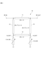
- Fig. 4 is a circuit diagram showing an example of the phase shifter according to the present embodiment
- Fig. 5 is a circuit diagram showing another example of the phase shifter according to the present embodiment.
- the phase shifter 10 shown in Fig. 4 is a hybrid coupled type radio frequency (RF) phase shifter composed of quarter wavelength lines 11 and 12 with a characteristic impedance of Z0 and quarter wavelength lines 13 and 14 with a characteristic impedance of Z0/ ⁇ 2.
- RF radio frequency
- one end of the line 11 is an input terminal RF_IN
- the other end of the line 11 is an output terminal RF_OUT.
- the phase shifter 10 includes the variable reactance elements 1 (1A, 1B) described above that terminate the output terminal 13_OUT on the line 13 side and the output terminal 14_OUT on the line 14 side, respectively.
- phase shifter 10 the RF signal input from input terminal RF_IN is distributed by hybrid coupled lines 11, 12, 13, and 14, and transmitted to output terminal 13_OUT on the line 13 side and output terminal 14_OUT on the line 14 side. Since these output terminals 13_OUT and 14_OUT are terminated by the variable reactance element 1 (1A, 1B) described above, the signals transmitted to these output terminals are reflected with a phase change that depends on the reactance of variable reactance element 1 (1A, 1B). The signals reflected at these output terminals 13_OUT and 14_OUT are recombined by hybrid coupled lines 11, 12, 13, and 14, and output from output terminal RF_OUT. At this time, the output signal undergoes a phase change that depends on the reactance of the variable reactance element 1 (1A, 1B) described above, and by changing the reactance of the variable reactance element described above, it operates as a phase shifter.
- FIG. 4 shows an example in which the above-mentioned variable reactance element 1 (1A, 1B) is applied to a hybrid coupled type phase shifter 10, as shown in FIG. 5, the above-mentioned variable reactance element 1 (1A, 1B) may also be applied to a loaded line type phase shifter 10 composed of a quarter-wavelength line 11 with a characteristic impedance of Z0.
- FIG. 6 is a diagram showing the design of an example of the phase shifter shown in FIG. 4.
- the phase shift amount ps of the phase shifter shown in FIG. 4 was measured using a network analyzer while varying the capacitance C of the digital capacitor or the inductance L of the digital inductor.
- a phase shift characteristic of approximately 360° was obtained.
- the reactance can be widely varied to both capacitive and inductive, making it possible to realize a low-loss high-frequency (RF) phase shifter with a large phase shift range.
- RF high-frequency
- Fig. 7 is a circuit diagram showing an example of an impedance matching circuit according to the present embodiment.
- the impedance matching circuit 20 shown in Fig. 7 includes an inductor 21 connected in series between one input terminal RF_IN+ of a pair of input terminals RF_IN+, RF_IN- and one output terminal RF_OUT+ of a pair of output terminals RF_OUT+, RF_OUT-, and the variable reactance element 1 (1A, 1B) described above connected between the pair of input terminals RF_IN+, RF_IN- and between the pair of output terminals RF_OUT+, RF_OUT-, respectively.
- the impedance matching circuit 20 operates as an impedance matching circuit by changing the impedance of the variable reactance element 1 (1A, 1B) described above.
- the reactance can be widely varied in both capacitive and inductive directions, making it possible to realize an impedance matching circuit with low loss and a wide impedance adjustment range.
Landscapes
- Networks Using Active Elements (AREA)
Priority Applications (4)
| Application Number | Priority Date | Filing Date | Title |
|---|---|---|---|
| CN202380066671.5A CN119923794A (zh) | 2022-12-02 | 2023-09-11 | 数字式可变电抗元件、移相器以及阻抗匹配电路 |
| JP2024561183A JPWO2024116538A1 (https=) | 2022-12-02 | 2023-09-11 | |
| EP23897197.2A EP4629435A1 (en) | 2022-12-02 | 2023-09-11 | Digital variable reactance element, phase shifter, and impedance matching circuit |
| US18/802,007 US20240405751A1 (en) | 2022-12-02 | 2024-08-13 | Digital variable reactance element, phase shifter, and impedance matching circuit |
Applications Claiming Priority (2)
| Application Number | Priority Date | Filing Date | Title |
|---|---|---|---|
| JP2022-193674 | 2022-12-02 | ||
| JP2022193674 | 2022-12-02 |
Related Child Applications (1)
| Application Number | Title | Priority Date | Filing Date |
|---|---|---|---|
| US18/802,007 Continuation US20240405751A1 (en) | 2022-12-02 | 2024-08-13 | Digital variable reactance element, phase shifter, and impedance matching circuit |
Publications (1)
| Publication Number | Publication Date |
|---|---|
| WO2024116538A1 true WO2024116538A1 (ja) | 2024-06-06 |
Family
ID=91323559
Family Applications (1)
| Application Number | Title | Priority Date | Filing Date |
|---|---|---|---|
| PCT/JP2023/033010 Ceased WO2024116538A1 (ja) | 2022-12-02 | 2023-09-11 | デジタル式可変リアクタンス素子、移相器およびインピーダンス整合回路 |
Country Status (5)
| Country | Link |
|---|---|
| US (1) | US20240405751A1 (https=) |
| EP (1) | EP4629435A1 (https=) |
| JP (1) | JPWO2024116538A1 (https=) |
| CN (1) | CN119923794A (https=) |
| WO (1) | WO2024116538A1 (https=) |
Citations (4)
| Publication number | Priority date | Publication date | Assignee | Title |
|---|---|---|---|---|
| JPH0974325A (ja) | 1995-09-04 | 1997-03-18 | Nippon Telegr & Teleph Corp <Ntt> | 可変リアクタンス素子およびこれを用いた移相回路 |
| JP2014530543A (ja) * | 2011-09-13 | 2014-11-17 | クゥアルコム・インコーポレイテッドQualcomm Incorporated | 複数の構成を有するインピーダンス整合回路 |
| WO2015178204A1 (ja) * | 2014-05-19 | 2015-11-26 | 株式会社村田製作所 | アンテナ整合回路、アンテナ整合モジュール、アンテナ装置および無線通信装置 |
| JP2022110070A (ja) * | 2014-12-19 | 2022-07-28 | マサチューセッツ インスティテュート オブ テクノロジー | 位相スイッチト素子を使用したチューニング可能整合ネットワーク |
Family Cites Families (11)
| Publication number | Priority date | Publication date | Assignee | Title |
|---|---|---|---|---|
| US3794941A (en) * | 1972-05-08 | 1974-02-26 | Hughes Aircraft Co | Automatic antenna impedance tuner including digital control circuits |
| JPH11168354A (ja) * | 1997-12-04 | 1999-06-22 | Mitsubishi Electric Corp | 可変移相器 |
| EP1514285B1 (en) * | 2002-06-05 | 2011-08-10 | Nxp B.V. | Electronic device and method of matching the impedance thereof |
| JP4975824B2 (ja) * | 2007-10-18 | 2012-07-11 | パイオニア株式会社 | 静電容量検出装置 |
| US7986924B2 (en) * | 2007-10-31 | 2011-07-26 | Lg Electronics Inc. | Impedance control apparatus and method for portable mobile communication terminal |
| US8803631B2 (en) * | 2010-03-22 | 2014-08-12 | Blackberry Limited | Method and apparatus for adapting a variable impedance network |
| JP2013026847A (ja) * | 2011-07-21 | 2013-02-04 | Hitachi Kokusai Electric Inc | アンテナインピーダンス整合方法 |
| FR3028691B1 (fr) * | 2014-11-13 | 2019-08-16 | Commissariat A L'energie Atomique Et Aux Energies Alternatives | Procede et module d'adaptation automatique d'impedance, en particulier pour une chaine d'emission ou reception radiofrequence |
| US10790784B2 (en) * | 2014-12-19 | 2020-09-29 | Massachusetts Institute Of Technology | Generation and synchronization of pulse-width modulated (PWM) waveforms for radio-frequency (RF) applications |
| CN109196782A (zh) * | 2016-05-20 | 2019-01-11 | 株式会社村田制作所 | 阻抗匹配电路、高频前端电路以及通信装置 |
| EP3751746B1 (en) * | 2017-12-28 | 2024-02-14 | Solaredge Technologies Ltd. | Variable impedance circuit |
-
2023
- 2023-09-11 CN CN202380066671.5A patent/CN119923794A/zh active Pending
- 2023-09-11 WO PCT/JP2023/033010 patent/WO2024116538A1/ja not_active Ceased
- 2023-09-11 JP JP2024561183A patent/JPWO2024116538A1/ja active Pending
- 2023-09-11 EP EP23897197.2A patent/EP4629435A1/en active Pending
-
2024
- 2024-08-13 US US18/802,007 patent/US20240405751A1/en active Pending
Patent Citations (4)
| Publication number | Priority date | Publication date | Assignee | Title |
|---|---|---|---|---|
| JPH0974325A (ja) | 1995-09-04 | 1997-03-18 | Nippon Telegr & Teleph Corp <Ntt> | 可変リアクタンス素子およびこれを用いた移相回路 |
| JP2014530543A (ja) * | 2011-09-13 | 2014-11-17 | クゥアルコム・インコーポレイテッドQualcomm Incorporated | 複数の構成を有するインピーダンス整合回路 |
| WO2015178204A1 (ja) * | 2014-05-19 | 2015-11-26 | 株式会社村田製作所 | アンテナ整合回路、アンテナ整合モジュール、アンテナ装置および無線通信装置 |
| JP2022110070A (ja) * | 2014-12-19 | 2022-07-28 | マサチューセッツ インスティテュート オブ テクノロジー | 位相スイッチト素子を使用したチューニング可能整合ネットワーク |
Non-Patent Citations (1)
| Title |
|---|
| See also references of EP4629435A1 |
Also Published As
| Publication number | Publication date |
|---|---|
| JPWO2024116538A1 (https=) | 2024-06-06 |
| EP4629435A1 (en) | 2025-10-08 |
| US20240405751A1 (en) | 2024-12-05 |
| CN119923794A (zh) | 2025-05-02 |
Similar Documents
| Publication | Publication Date | Title |
|---|---|---|
| US5039873A (en) | Microwave elements with impedance control circuits | |
| US10211801B2 (en) | Hybrid coupler with phase and attenuation control | |
| CN109921761B (zh) | 一种具有通带可调和可开关功能的可重构滤波器 | |
| JP2007532060A (ja) | 電子制御されたデジタル/アナログ混載移相器 | |
| JP2008187661A (ja) | 移相器、ビット移相器 | |
| CN111224653A (zh) | 单刀双掷开关 | |
| CN110190830A (zh) | 一种双频带小型化数字移相器 | |
| US20110199141A1 (en) | Phase shifter and control method thereof | |
| US20040145429A1 (en) | Phase shifter and multibit phase shifter | |
| CN111130488A (zh) | 一种超宽带移相电路 | |
| US4639691A (en) | Oscillator | |
| WO2024116538A1 (ja) | デジタル式可変リアクタンス素子、移相器およびインピーダンス整合回路 | |
| JPH10256809A (ja) | 電子同調型有極フィルタ | |
| EP1098432B1 (en) | Frequency-switching oscillator and electronic device using the same | |
| US11575188B2 (en) | Phase shifter | |
| US8031018B2 (en) | Oscillator with coupled amplifier | |
| JPH08213802A (ja) | 高周波スイッチ回路 | |
| CN1371167A (zh) | 切换压控振荡器振荡频带的压控可变调谐电路 | |
| WO2024116539A1 (ja) | Rf移相器 | |
| US20050057322A1 (en) | Apparatus and method for combining electrical signals | |
| KR100386175B1 (ko) | 전압제어발진기 | |
| JP7279795B2 (ja) | 電圧制御発振器 | |
| JPH11205086A (ja) | 移相器 | |
| Abdalla et al. | A tunable metamaterial phase-shifter structure based on a 0.13 μm CMOS active inductor | |
| He et al. | A Wideband 360° Filtering Phase Shifter With Continuous Phase Shift |
Legal Events
| Date | Code | Title | Description |
|---|---|---|---|
| 121 | Ep: the epo has been informed by wipo that ep was designated in this application |
Ref document number: 23897197 Country of ref document: EP Kind code of ref document: A1 |
|
| WWE | Wipo information: entry into national phase |
Ref document number: 2024561183 Country of ref document: JP |
|
| WWE | Wipo information: entry into national phase |
Ref document number: 202380066671.5 Country of ref document: CN |
|
| WWP | Wipo information: published in national office |
Ref document number: 202380066671.5 Country of ref document: CN |
|
| WWE | Wipo information: entry into national phase |
Ref document number: 2023897197 Country of ref document: EP |
|
| NENP | Non-entry into the national phase |
Ref country code: DE |
|
| ENP | Entry into the national phase |
Ref document number: 2023897197 Country of ref document: EP Effective date: 20250702 |
|
| WWP | Wipo information: published in national office |
Ref document number: 2023897197 Country of ref document: EP |