WO2024116538A1 - デジタル式可変リアクタンス素子、移相器およびインピーダンス整合回路 - Google Patents
デジタル式可変リアクタンス素子、移相器およびインピーダンス整合回路 Download PDFInfo
- Publication number
- WO2024116538A1 WO2024116538A1 PCT/JP2023/033010 JP2023033010W WO2024116538A1 WO 2024116538 A1 WO2024116538 A1 WO 2024116538A1 JP 2023033010 W JP2023033010 W JP 2023033010W WO 2024116538 A1 WO2024116538 A1 WO 2024116538A1
- Authority
- WO
- WIPO (PCT)
- Prior art keywords
- digital
- variable reactance
- reactance element
- variable
- phase shifter
- Prior art date
Links
- 239000003990 capacitor Substances 0.000 claims abstract description 54
- 238000010586 diagram Methods 0.000 description 13
- 230000010363 phase shift Effects 0.000 description 6
- 230000005669 field effect Effects 0.000 description 3
- 230000001939 inductive effect Effects 0.000 description 3
- 230000004048 modification Effects 0.000 description 3
- 238000012986 modification Methods 0.000 description 3
- 238000002595 magnetic resonance imaging Methods 0.000 description 2
- 238000001514 detection method Methods 0.000 description 1
Images


Classifications
-
- H—ELECTRICITY
- H03—ELECTRONIC CIRCUITRY
- H03H—IMPEDANCE NETWORKS, e.g. RESONANT CIRCUITS; RESONATORS
- H03H11/00—Networks using active elements
- H03H11/02—Multiple-port networks
- H03H11/16—Networks for phase shifting
-
- H—ELECTRICITY
- H01—ELECTRIC ELEMENTS
- H01P—WAVEGUIDES; RESONATORS, LINES, OR OTHER DEVICES OF THE WAVEGUIDE TYPE
- H01P1/00—Auxiliary devices
- H01P1/18—Phase-shifters
-
- H—ELECTRICITY
- H03—ELECTRONIC CIRCUITRY
- H03H—IMPEDANCE NETWORKS, e.g. RESONANT CIRCUITS; RESONATORS
- H03H11/00—Networks using active elements
- H03H11/02—Multiple-port networks
- H03H11/28—Impedance matching networks
-
- H—ELECTRICITY
- H03—ELECTRONIC CIRCUITRY
- H03H—IMPEDANCE NETWORKS, e.g. RESONANT CIRCUITS; RESONATORS
- H03H11/00—Networks using active elements
- H03H11/46—One-port networks
-
- H—ELECTRICITY
- H03—ELECTRONIC CIRCUITRY
- H03H—IMPEDANCE NETWORKS, e.g. RESONANT CIRCUITS; RESONATORS
- H03H7/00—Multiple-port networks comprising only passive electrical elements as network components
- H03H7/18—Networks for phase shifting
- H03H7/20—Two-port phase shifters providing an adjustable phase shift
-
- H—ELECTRICITY
- H03—ELECTRONIC CIRCUITRY
- H03H—IMPEDANCE NETWORKS, e.g. RESONANT CIRCUITS; RESONATORS
- H03H7/00—Multiple-port networks comprising only passive electrical elements as network components
- H03H7/38—Impedance-matching networks
Definitions
- the present invention relates to a digitally variable reactance element, a phase shifter, and an impedance matching circuit.
- variable reactance elements are used in phase shifters used in microwave circuits.
- Known examples of such variable reactance elements include variable capacitors, varicaps, varactor diodes, and other variable capacitors (see, for example, Patent Document 1).
- variable reactance element With a larger variable width of reactance (1/2 ⁇ fc) is required.
- variable reactance element is a variable inductor.
- conventional variable reactance elements only use either a variable capacitor or a variable inductor.
- the reactance (impedance) changes in the direction of the arrow D_C.
- the reactance (impedance) changes in the direction of the arrow D_L. In this way, the change in reactance caused by a variable capacitor and the change in reactance caused by a variable inductor are mutually different, unidirectional changes.
- the present invention aims to provide a digital variable reactance element, phase shifter, and impedance matching circuit with a wide variable range.
- the digital variable reactance element of the present invention is a digital variable reactance element that digitally varies reactance, and includes a plurality of digital capacitors and a plurality of digital inductors.
- the plurality of digital capacitors and the plurality of digital inductors are connected in series or in parallel.
- Each of the plurality of digital capacitors has a capacitor and a first digital switch connected in series or in parallel, and the first digital switch can be switched between two states, an on state or an off state.
- Each of the plurality of digital inductors has an inductor and a second digital switch connected in series or in parallel, and the second digital switch can be switched between two states, an on state or an off state.
- the phase shifter according to the present invention includes the digitally variable reactance element described above, and generates an output signal in which the phase of the input signal is digitally varied.
- the impedance matching circuit of the present invention includes the digitally variable reactance element described above, and matches the characteristic impedance of the connected line.
- variable range of a digital variable reactance element it is possible to widen the phase shift range of a phase shifter. Also, according to the present invention, it is possible to widen the matching range of an impedance matching circuit.
- FIG. 1 is a circuit diagram showing a digital variable reactance element according to an embodiment of the present invention.
- FIG. 11 is a circuit diagram showing a digital variable reactance element according to a first modified example of the present embodiment.
- FIG. 11 is a circuit diagram showing a digital variable reactance element according to a second modified example of the present embodiment.
- FIG. 2 is a circuit diagram illustrating an example of a phase shifter according to the present embodiment.
- FIG. 11 is a circuit diagram showing another example of the phase shifter according to the present embodiment.
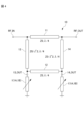
- FIG. 5 illustrates an example design of the phase shifter shown in FIG. 4 .
- 1 is a circuit diagram showing an example of an impedance matching circuit according to an embodiment of the present invention.
- FIG. 2 is a Smith chart illustrating an example of reactance characteristics.
- Fig. 1 is a circuit diagram showing a digital variable reactance element according to the present embodiment.
- the digital variable reactance element 1 is an element that digitally varies reactance.
- the digital variable reactance element 1 includes a plurality of digital capacitors 2 and a plurality of digital inductors 4.
- the digital variable reactance element 1 may also include a digital resistor 6.
- the plurality of digital capacitors 2, the plurality of digital inductors 4, and the digital resistor 6 are connected in parallel.
- the digital capacitor 2 has a capacitor C1 and a digital switch (first digital switch) Q connected in series.
- the digital switch Q is not particularly limited, but a switching element such as a FET (Field Effect Transistor) can be used.
- the digital switch Q can be switched between two states: on and off. This allows the digital capacitor 2 to be switched between two values: a first value which is the capacitance of the capacitor C1 (digital switch Q is on), or a second value which is a capacitance of 0 (digital switch Q is off). In other words, the digital capacitor 2 can digitally switch capacitance.
- the digital inductor 4 has an inductor L1 and a digital switch (second digital switch) Q connected in series.
- the digital switch Q is not particularly limited, but may be a switching element such as a FET (Field Effect Transistor).
- the digital switch Q can be switched between two states: on and off. This allows the digital inductor 4 to be switched between two values: a first value which is the inductance of the inductor L1 (digital switch Q is on), or a second value which is an inductance of 0 (digital switch Q is off). In other words, the digital inductor 4 is capable of digitally switching the inductance.
- the digital resistor 6 has a resistor R1 and a digital switch Q connected in series.
- the digital switch Q is not particularly limited, but may be a switching element such as a FET (Field Effect Transistor).
- the digital switch Q can be switched between two states: on and off. This allows the digital resistor 6 to be switched between two values: a first value which is the resistance value of the resistor R1 (digital switch Q is on), or a second value which is a resistance value of 0 (digital switch Q is off). In other words, the digital resistor 6 is capable of digitally switching the resistance value.
- variable reactance element 1 can digitally vary the reactance by switching the digital switches Q between on and off. Furthermore, the variable reactance element 1 can digitally vary its impedance, particularly its impedance to an RF signal (radio frequency signal), by switching the digital switches Q between on and off.
- RF signal radio frequency signal
- the reactance of the multiple capacitors C1 and multiple inductors L1 is digitally variable by control of the digital switch Q.
- the impedance of the multiple capacitors C1, multiple inductors L1, and resistor R1 is digitally variable by control of the digital switch Q.
- variable capacitors or multiple variable inductors are not used, and the control signals for the multiple variable capacitors or multiple variable inductors do not become complicated.
- variable reactance element 1 is exemplified in which each digital capacitor 2 has a capacitor C1 and a digital switch Q connected in series, each digital inductor 4 has an inductor and a digital switch connected in series or parallel, and multiple digital capacitors 2 and multiple digital inductors 4 are connected in parallel.
- the present invention is not limited to this, and can be applied to various variable reactance elements in which each digital capacitor has a capacitor and a digital switch connected in series or parallel, each digital inductor has an inductor and a digital switch connected in series or parallel, and multiple digital capacitors and multiple digital inductors are connected in series or parallel.
- modified examples 1 and 2 of this embodiment are given below.
- FIG. 2 is a circuit diagram showing a digital variable reactance element according to a first modified example of this embodiment.
- the digital variable reactance element 1A is an element that digitally varies reactance.
- the digital variable reactance element 1A includes a plurality of digital capacitors 2A and a plurality of digital inductors 4A.
- the digital variable reactance element 1A may also include a digital resistor 6A.
- the plurality of digital capacitors 2A, the plurality of digital inductors 4A, and the digital resistor 6A are connected in series.
- the digital capacitor 2A has a capacitor C1 and a digital switch (first digital switch) Q connected in series, and also has a capacitor C2 and the digital switch Q connected in parallel. Specifically, in the digital capacitor 2A, the series circuit of the capacitor C1 and the digital switch Q and the capacitor C2 are connected in parallel.
- the digital switch Q is the same as described above. This allows the digital capacitor 2A to be switched between two values: a first value (digital switch Q is on) which is the combined capacitance of the capacitors C1 and C2, or a second value (digital switch Q is off) which is the capacitance of the capacitor C2. In other words, the digital capacitor 2A is capable of digitally switching capacitance.
- the digital inductor 4A has an inductor L1 and a digital switch (second digital switch) Q connected in series, and also has an inductor L2 and the digital switch Q connected in parallel. Specifically, in the digital inductor 4A, the series circuit of the inductor L1 and the digital switch Q and the inductor L2 are connected in parallel.
- the digital switch Q is the same as described above. This allows the digital inductor 4A to be switched between two values: a first value (digital switch Q is on) which is the combined inductance of inductor L1 and inductor L2, and a second value (digital switch Q is off) which is the inductance of inductor L2. In other words, the digital inductor 4A is capable of digitally switching inductance.
- the digital resistor 6A has a resistor R1 and a digital switch Q connected in parallel.
- the digital switch Q is the same as described above. This allows the digital resistor 6A to be switched between two values: a first value that is a resistance value of 0 (digital switch Q is on), and a second value that is the resistance value of resistor R1 (digital switch Q is off). In other words, the digital resistor 6A is capable of digitally switching the resistance value.
- variable reactance element 1A can digitally vary the reactance by switching the digital switches Q between on and off. Furthermore, the variable reactance element 1A can digitally vary the impedance, particularly the impedance to an RF signal (radio frequency signal), by switching the on or off state of each digital switch Q.
- RF signal radio frequency signal
- the digital variable reactance element 1A of this modified example 1 has the same advantages as the digital variable reactance element 1 of this embodiment described above.
- FIG. 3 is a circuit diagram showing a digital variable reactance element according to a second modified example of this embodiment.
- the digital variable reactance element 1B is an element that digitally varies reactance.
- the digital variable reactance element 1B includes a plurality of the above-mentioned digital capacitors 2A and a plurality of the above-mentioned digital inductors 4.
- the plurality of digital capacitors 2A are connected in series
- the plurality of digital inductors 4 are connected in parallel
- the series circuit of the digital capacitors 2A and the parallel circuit of the digital inductors 4 are connected in series.
- variable reactance element 1B can digitally vary the reactance by switching the digital switches Q between on and off. Furthermore, the variable reactance element 1B can digitally vary its impedance, particularly the impedance to an RF signal (radio frequency signal), by switching the digital switches Q between on and off.
- RF signal radio frequency signal
- the digital variable reactance element 1B of this modified example 2 has the same advantages as the digital variable reactance element 1 of this embodiment described above.
- phase shifter and an impedance matching circuit will be described as examples of devices to which the above-mentioned digital variable reactance element is applied.
- the digital variable reactance element of this embodiment is not limited to these, and can be applied to various devices that require variable reactance or impedance, such as variable loads, MRI (Magnetic Resonance Imaging) detection circuits, VCOs (Voltage Controlled Oscillators), phase-locked loop circuits, and frequency synthesizers.
- Fig. 4 is a circuit diagram showing an example of the phase shifter according to the present embodiment
- Fig. 5 is a circuit diagram showing another example of the phase shifter according to the present embodiment.
- the phase shifter 10 shown in Fig. 4 is a hybrid coupled type radio frequency (RF) phase shifter composed of quarter wavelength lines 11 and 12 with a characteristic impedance of Z0 and quarter wavelength lines 13 and 14 with a characteristic impedance of Z0/ ⁇ 2.
- RF radio frequency
- one end of the line 11 is an input terminal RF_IN
- the other end of the line 11 is an output terminal RF_OUT.
- the phase shifter 10 includes the variable reactance elements 1 (1A, 1B) described above that terminate the output terminal 13_OUT on the line 13 side and the output terminal 14_OUT on the line 14 side, respectively.
- phase shifter 10 the RF signal input from input terminal RF_IN is distributed by hybrid coupled lines 11, 12, 13, and 14, and transmitted to output terminal 13_OUT on the line 13 side and output terminal 14_OUT on the line 14 side. Since these output terminals 13_OUT and 14_OUT are terminated by the variable reactance element 1 (1A, 1B) described above, the signals transmitted to these output terminals are reflected with a phase change that depends on the reactance of variable reactance element 1 (1A, 1B). The signals reflected at these output terminals 13_OUT and 14_OUT are recombined by hybrid coupled lines 11, 12, 13, and 14, and output from output terminal RF_OUT. At this time, the output signal undergoes a phase change that depends on the reactance of the variable reactance element 1 (1A, 1B) described above, and by changing the reactance of the variable reactance element described above, it operates as a phase shifter.
- FIG. 4 shows an example in which the above-mentioned variable reactance element 1 (1A, 1B) is applied to a hybrid coupled type phase shifter 10, as shown in FIG. 5, the above-mentioned variable reactance element 1 (1A, 1B) may also be applied to a loaded line type phase shifter 10 composed of a quarter-wavelength line 11 with a characteristic impedance of Z0.
- FIG. 6 is a diagram showing the design of an example of the phase shifter shown in FIG. 4.
- the phase shift amount ps of the phase shifter shown in FIG. 4 was measured using a network analyzer while varying the capacitance C of the digital capacitor or the inductance L of the digital inductor.
- a phase shift characteristic of approximately 360° was obtained.
- the reactance can be widely varied to both capacitive and inductive, making it possible to realize a low-loss high-frequency (RF) phase shifter with a large phase shift range.
- RF high-frequency
- Fig. 7 is a circuit diagram showing an example of an impedance matching circuit according to the present embodiment.
- the impedance matching circuit 20 shown in Fig. 7 includes an inductor 21 connected in series between one input terminal RF_IN+ of a pair of input terminals RF_IN+, RF_IN- and one output terminal RF_OUT+ of a pair of output terminals RF_OUT+, RF_OUT-, and the variable reactance element 1 (1A, 1B) described above connected between the pair of input terminals RF_IN+, RF_IN- and between the pair of output terminals RF_OUT+, RF_OUT-, respectively.
- the impedance matching circuit 20 operates as an impedance matching circuit by changing the impedance of the variable reactance element 1 (1A, 1B) described above.
- the reactance can be widely varied in both capacitive and inductive directions, making it possible to realize an impedance matching circuit with low loss and a wide impedance adjustment range.
Landscapes
- Networks Using Active Elements (AREA)
Abstract
可変幅が広いデジタル式可変リアクタンス素子を提供する。デジタル式可変リアクタンス素子1は、複数のデジタル式キャパシタ2と複数のデジタル式インダクタ4とを備え、複数のデジタル式キャパシタ2と複数のデジタル式インダクタ4とは、直列または並列に接続されており、複数のデジタル式キャパシタ2の各々は、直列または並列に接続されたキャパシタC1と第1デジタルスイッチQとを有し、第1デジタルスイッチQはオン状態またはオフ状態の2状態に切り換え可能であり、複数のデジタル式インダクタ4の各々は、直列または並列に接続されたインダクタL1と第2デジタルスイッチQとを有し、第2デジタルスイッチQはオン状態またはオフ状態の2状態に切り換え可能である。
Description
本発明は、デジタル式可変リアクタンス素子、移相器およびインピーダンス整合回路に関する。
例えば、マイクロ波回路で用いる移相器では、可変リアクタンス素子が用いられている。このような可変リアクタンス素子としては、バリアブルコンデンサ、バリキャップまたはバラクタダイオード等の可変キャパシタが知られている(例えば、特許文献1参照)。
高周波移相器のように周波数fが高くなると、移相器の移相幅が小さくなり、損失が大きくなる。そのため、より大きなリアクタンス(1/2πfc)の可変幅を有する可変リアクタンス素子が要求される。
ところで、可変リアクタンス素子としては、可変インダクタがある。しかし、従来の可変リアクタンス素子は、可変キャパシタおよび可変インダクタのいずれか一方のみを用いていた。
図8のスミスチャートに示すように、キャパシタを挿入すると、あるいはキャパシタンスが大きくなると、リアクタンス(インピーダンス)が矢印方向D_Cに変化する。一方、インダクタを挿入すると、あるいはインダクタンスが大きくなると、リアクタンス(インピーダンス)が矢印方向D_Lに変化する。このように、可変キャパシタによるリアクタンスの変化と可変インダクタによるリアクタンスの変化とは、互いに異なる片方向の変化である。
そのため、リアクタンスの可変幅をより広く制御する場合、複数の可変キャパシタまたは複数の可変インダクタを用いる必要があり、複数の可変キャパシタまたは複数の可変インダクタの制御信号が複雑であった。
そこで、本発明は、可変幅が広いデジタル式可変リアクタンス素子、移相器およびインピーダンス整合回路を提供することを目的とする。
本発明に係るデジタル式可変リアクタンス素子は、デジタル式にリアクタンスを可変するデジタル式可変リアクタンス素子であって、複数のデジタル式キャパシタと、複数のデジタル式インダクタとを備える。前記複数のデジタル式キャパシタと前記複数のデジタル式インダクタとは、直列または並列に接続されている。前記複数のデジタル式キャパシタの各々は、直列または並列に接続されたキャパシタと第1デジタルスイッチとを有し、前記第1デジタルスイッチはオン状態またはオフ状態の2状態に切り換え可能である。前記複数のデジタル式インダクタの各々は、直列または並列に接続されたインダクタと第2デジタルスイッチとを有し、前記第2デジタルスイッチはオン状態またはオフ状態の2状態に切り換え可能である。
本発明に係る移相器は、上記のデジタル式可変リアクタンス素子を備え、入力信号の位相をデジタル式に可変した出力信号を生成する。
本発明に係るインピーダンス整合回路は、上記のデジタル式可変リアクタンス素子を備え、接続された線路に対して特性インピーダンスを整合する。
本発明によれば、デジタル式可変リアクタンス素子の可変幅を広くすることができる。また、本発明によれば、移相器の移相幅を広くすることができる。また、本発明によれば、インピーダンス整合回路の整合幅を広くすることができる。
以下、添付の図面を参照して本発明の実施形態の一例について説明する。なお、各図面において同一または相当の部分に対しては同一の符号を附すこととする。
(本実施形態のデジタル式可変リアクタンス素子)
図1は、本実施形態に係るデジタル式可変リアクタンス素子を示す回路図である。図1に示すように、デジタル式可変リアクタンス素子1は、デジタル式にリアクタンスを可変する素子である。デジタル式可変リアクタンス素子1は、複数のデジタル式キャパシタ2と複数のデジタル式インダクタ4とを備える。なお、デジタル式可変リアクタンス素子1は、デジタル式抵抗器6を備えてもよい。デジタル式可変リアクタンス素子1において、複数のデジタル式キャパシタ2と、複数のデジタル式インダクタ4と、デジタル式抵抗器6とは並列に接続されている。
図1は、本実施形態に係るデジタル式可変リアクタンス素子を示す回路図である。図1に示すように、デジタル式可変リアクタンス素子1は、デジタル式にリアクタンスを可変する素子である。デジタル式可変リアクタンス素子1は、複数のデジタル式キャパシタ2と複数のデジタル式インダクタ4とを備える。なお、デジタル式可変リアクタンス素子1は、デジタル式抵抗器6を備えてもよい。デジタル式可変リアクタンス素子1において、複数のデジタル式キャパシタ2と、複数のデジタル式インダクタ4と、デジタル式抵抗器6とは並列に接続されている。
デジタル式キャパシタ2は、直列に接続されたキャパシタC1とデジタルスイッチ(第1デジタルスイッチ)Qとを有する。デジタルスイッチQとしては、特に限定されないが、FET(Field Effect Transistor)などのスイッチ素子が用いられる。デジタルスイッチQは、オン状態またはオフ状態の2状態に切り換え可能である。これにより、デジタル式キャパシタ2は、キャパシタC1のキャパシタンスである第1値(デジタルスイッチQがオン状態)、または、キャパシタンス0である第2値(デジタルスイッチQがオフ状態)の2値に切り換え可能である。すなわち、デジタル式キャパシタ2は、キャパシタンスをデジタル式に切り換え可能である。
デジタル式インダクタ4は、直列に接続されたインダクタL1とデジタルスイッチ(第2デジタルスイッチ)Qとを有する。デジタルスイッチQとしては、特に限定されないが、FET(Field Effect Transistor)などのスイッチ素子が用いられる。デジタルスイッチQは、オン状態またはオフ状態の2状態に切り換え可能である。これにより、デジタル式インダクタ4は、インダクタL1のインダクタンスである第1値(デジタルスイッチQがオン状態)、または、インダクタンス0である第2値(デジタルスイッチQがオフ状態)の2値に切り換え可能である。すなわち、デジタル式インダクタ4は、インダクタンスをデジタル式に切り換え可能である。
デジタル式抵抗器6は、直列に接続された抵抗器R1とデジタルスイッチQとを有する。デジタルスイッチQとしては、特に限定されないが、FET(Field Effect Transistor)などのスイッチ素子が用いられる。デジタルスイッチQは、オン状態またはオフ状態の2状態に切り換え可能である。これにより、デジタル式抵抗器6は、抵抗器R1の抵抗値である第1値(デジタルスイッチQがオン状態)、または、抵抗値0である第2値(デジタルスイッチQがオフ状態)の2値に切り換え可能である。すなわち、デジタル式抵抗器6は、抵抗値をデジタル式に切り換え可能である。
これにより、可変リアクタンス素子1は、各デジタルスイッチQのオン状態またはオフ状態が切り替えられることにより、リアクタンスをデジタル式に可変することができる。
また、可変リアクタンス素子1は、各デジタルスイッチQのオン状態またはオフ状態が切り替えられることにより、インピーダンス、特にRF信号(高周波信号)に対するインピーダンス、をデジタル式に可変することができる。
また、可変リアクタンス素子1は、各デジタルスイッチQのオン状態またはオフ状態が切り替えられることにより、インピーダンス、特にRF信号(高周波信号)に対するインピーダンス、をデジタル式に可変することができる。
以上説明したよう、本実施形態のデジタル式可変リアクタンス素子1によれば、複数のキャパシタC1および複数のインダクタL1によるリアクタンスを、デジタルスイッチQによる制御によりデジタル式に可変する。また、デジタル式可変リアクタンス素子1によれば、複数のキャパシタC1、複数のインダクタL1および抵抗器R1によるインピーダンスを、デジタルスイッチQによる制御によりデジタル式に可変する。
また、キャパシタンスの可変だけでなくインダクタンスの可変も可能であり、リアクタンスを容量性(1/2πfc)から誘導性(2πfL)まで幅広く可変することができる。そのため、リアクタンス(1/2πfc+2πfL)の可変幅を広くすることができる。
また、複数の可変キャパシタまたは複数の可変インダクタを用いることがなく、複数の可変キャパシタまたは複数の可変インダクタの制御信号が複雑になることがない。
また、低損失で、移相幅が大きい高周波(RF)移相器を実現することが可能となる。
上述した実施形態では、各デジタル式キャパシタ2が直列に接続されたキャパシタC1とデジタルスイッチQとを有し、各デジタル式インダクタ4が直列または並列に接続されたインダクタとデジタルスイッチとを有し、複数のデジタル式キャパシタ2と複数のデジタル式インダクタ4とが並列に接続された可変リアクタンス素子1を例示した。しかし、本発明は、これに限定されず、各デジタル式キャパシタが直列または並列に接続されたキャパシタとデジタルスイッチとを有し、各デジタル式インダクタが直列または並列に接続されたインダクタとデジタルスイッチとを有し、複数のデジタル式キャパシタと複数のデジタル式インダクタとが直列または並列に接続された種々の可変リアクタンス素子に適用可能である。例えば、以下に本実施形態の変形例1,2について例示する。
(変形例1のデジタル式可変リアクタンス素子)
図2は、本実施形態の変形例1に係るデジタル式可変リアクタンス素子を示す回路図である。図2に示すように、デジタル式可変リアクタンス素子1Aは、デジタル式にリアクタンスを可変する素子である。デジタル式可変リアクタンス素子1Aは、複数のデジタル式キャパシタ2Aと複数のデジタル式インダクタ4Aとを備える。なお、デジタル式可変リアクタンス素子1Aは、デジタル式抵抗器6Aを備えてもよい。デジタル式可変リアクタンス素子1Aにおいて、複数のデジタル式キャパシタ2Aと、複数のデジタル式インダクタ4Aと、デジタル式抵抗器6Aとは直列に接続されている。
図2は、本実施形態の変形例1に係るデジタル式可変リアクタンス素子を示す回路図である。図2に示すように、デジタル式可変リアクタンス素子1Aは、デジタル式にリアクタンスを可変する素子である。デジタル式可変リアクタンス素子1Aは、複数のデジタル式キャパシタ2Aと複数のデジタル式インダクタ4Aとを備える。なお、デジタル式可変リアクタンス素子1Aは、デジタル式抵抗器6Aを備えてもよい。デジタル式可変リアクタンス素子1Aにおいて、複数のデジタル式キャパシタ2Aと、複数のデジタル式インダクタ4Aと、デジタル式抵抗器6Aとは直列に接続されている。
デジタル式キャパシタ2Aは、直列に接続されたキャパシタC1とデジタルスイッチ(第1デジタルスイッチ)Qとを有し、また、並列に接続されたキャパシタC2と当該デジタルスイッチQとを有する。具体的には、デジタル式キャパシタ2Aにおいて、キャパシタC1とデジタルスイッチQとの直列回路と、キャパシタC2とが、並列に接続されている。デジタルスイッチQとしては上述同様である。これにより、デジタル式キャパシタ2Aは、キャパシタC1とキャパシタC2との合成キャパシタンスである第1値(デジタルスイッチQがオン状態)、または、キャパシタC2のキャパシタンスである第2値(デジタルスイッチQがオフ状態)の2値に切り換え可能である。すなわち、デジタル式キャパシタ2Aは、キャパシタンスをデジタル式に切り換え可能である。
デジタル式インダクタ4Aは、直列に接続されたインダクタL1とデジタルスイッチ(第2デジタルスイッチ)Qとを有し、また、並列に接続されたインダクタL2と当該デジタルスイッチQとを有する。具体的には、デジタル式インダクタ4Aにおいて、インダクタL1とデジタルスイッチQとの直列回路と、インダクタL2とが、並列に接続されている。デジタルスイッチQとしては上述同様である。これにより、デジタル式インダクタ4Aは、インダクタL1とインダクタL2との合成インダクタンスである第1値(デジタルスイッチQがオン状態)、または、インダクタL2のインダクタンスである第2値(デジタルスイッチQがオフ状態)の2値に切り換え可能である。すなわち、デジタル式インダクタ4Aは、インダクタンスをデジタル式に切り換え可能である。
デジタル式抵抗器6Aは、並列に接続された抵抗器R1とデジタルスイッチQとを有する。デジタルスイッチQとしては上述同様である。これにより、デジタル式抵抗器6Aは、抵抗値0である第1値(デジタルスイッチQがオン状態)、または、抵抗器R1の抵抗値である第2値(デジタルスイッチQがオフ状態)の2値に切り換え可能である。すなわち、デジタル式抵抗器6Aは、抵抗値をデジタル式に切り換え可能である。
これにより、可変リアクタンス素子1Aは、各デジタルスイッチQのオン状態またはオフ状態が切り替えられることにより、リアクタンスをデジタル式に可変することができる。
また、可変リアクタンス素子1Aは、各デジタルスイッチQのオン状態またはオフ状態が切り替えられることにより、インピーダンス、特にRF信号(高周波信号)に対するインピーダンス、をデジタル式に可変することができる。
また、可変リアクタンス素子1Aは、各デジタルスイッチQのオン状態またはオフ状態が切り替えられることにより、インピーダンス、特にRF信号(高周波信号)に対するインピーダンス、をデジタル式に可変することができる。
この変形例1のデジタル式可変リアクタンス素子1Aでも、上述した本実施形態のデジタル式可変リアクタンス素子1と同様の利点を有する。
(変形例2のデジタル式可変リアクタンス素子)
図3は、本実施形態の変形例2に係るデジタル式可変リアクタンス素子を示す回路図である。図3に示すように、デジタル式可変リアクタンス素子1Bは、デジタル式にリアクタンスを可変する素子である。デジタル式可変リアクタンス素子1Bは、複数の上述のデジタル式キャパシタ2Aと複数の上述のデジタル式インダクタ4とを備える。デジタル式可変リアクタンス素子1Bにおいて、複数のデジタル式キャパシタ2Aは直列に接続されており、複数のデジタル式インダクタ4は並列に接続されており、デジタル式キャパシタ2Aの直列回路とデジタル式インダクタ4の並列回路は直列に接続されている。
図3は、本実施形態の変形例2に係るデジタル式可変リアクタンス素子を示す回路図である。図3に示すように、デジタル式可変リアクタンス素子1Bは、デジタル式にリアクタンスを可変する素子である。デジタル式可変リアクタンス素子1Bは、複数の上述のデジタル式キャパシタ2Aと複数の上述のデジタル式インダクタ4とを備える。デジタル式可変リアクタンス素子1Bにおいて、複数のデジタル式キャパシタ2Aは直列に接続されており、複数のデジタル式インダクタ4は並列に接続されており、デジタル式キャパシタ2Aの直列回路とデジタル式インダクタ4の並列回路は直列に接続されている。
これにより、可変リアクタンス素子1Bは、各デジタルスイッチQのオン状態またはオフ状態が切り替えられることにより、リアクタンスをデジタル式に可変することができる。
また、可変リアクタンス素子1Bは、各デジタルスイッチQのオン状態またはオフ状態が切り替えられることにより、インピーダンス、特にRF信号(高周波信号)に対するインピーダンス、をデジタル式に可変することができる。
また、可変リアクタンス素子1Bは、各デジタルスイッチQのオン状態またはオフ状態が切り替えられることにより、インピーダンス、特にRF信号(高周波信号)に対するインピーダンス、をデジタル式に可変することができる。
この変形例2のデジタル式可変リアクタンス素子1Bでも、上述した本実施形態のデジタル式可変リアクタンス素子1と同様の利点を有する。
以下では、上述したデジタル式可変リアクタンス素子を適用するデバイスの一例として、移相器およびインピーダンス整合回路について説明する。なお、本実施形態のデジタル式可変リアクタンス素子は、これらに限定されず、例えば、可変負荷、MRI(Magnetic Resonance Imaging)の検波回路、VCO(Voltage Controlled Oscillator)、位相同期回路および周波数シンセサイザ等の、リアクタンスまたはインピーダンスの可変を要する種々のデバイスに適用可能である。
(本実施形態の移相器)
図4は、本実施形態に係る移相器の一例を示す回路図であり、図5は、本実施形態に係る移相器の他の一例を示す回路図である。図4に示す移相器10は、特性インピーダンスがZ0の1/4波長線路11,12および特性インピーダンスがZ0/√2の1/4波長線路13,14で構成されたハイブリッドカップルド(Hybrid Coupled)型の高周波(RF)移相器である。移相器10は、線路11の一端側を入力端子RF_INとし、線路11の他端側を出力端子RF_OUTとする。移相器10は、線路13側の出力端子13_OUTと線路14側の出力端子14_OUTとをそれぞれ終端する上述した可変リアクタンス素子1(1A,1B)を備える。
図4は、本実施形態に係る移相器の一例を示す回路図であり、図5は、本実施形態に係る移相器の他の一例を示す回路図である。図4に示す移相器10は、特性インピーダンスがZ0の1/4波長線路11,12および特性インピーダンスがZ0/√2の1/4波長線路13,14で構成されたハイブリッドカップルド(Hybrid Coupled)型の高周波(RF)移相器である。移相器10は、線路11の一端側を入力端子RF_INとし、線路11の他端側を出力端子RF_OUTとする。移相器10は、線路13側の出力端子13_OUTと線路14側の出力端子14_OUTとをそれぞれ終端する上述した可変リアクタンス素子1(1A,1B)を備える。
移相器10において、入力端子RF_INから入力されたRF信号は、ハイブリッドカップルド(Hybrid Coupled)型の線路11,12,13,14で分配され、線路13側の出力端子13_OUTと線路14側の出力端子14_OUTとに伝達される。これらの出力端子13_OUT,14_OUTは上述した可変リアクタンス素子1(1A,1B)により終端されているため、これらの出力端子に伝達された信号は可変リアクタンス素子1(1A,1B)のリアクタンス量に依存した位相変化をうけ反射される。これらの出力端子13_OUT,14_OUTにて反射された信号はハイブリッドカップルド(Hybrid Coupled)型の線路11,12,13,14で再び合成され出力端子RF_OUTから出力される。このとき、出力信号は上述した可変リアクタンス素子1(1A,1B)のリアクタンス量に依存した位相変化を受けており、上述した可変リアクタンス素子のリアクタンス量を変化させることにより移相器として動作する。
なお、図4では、ハイブリッドカップルド(Hybrid Coupled)型の移相器10に上述した可変リアクタンス素子1(1A,1B)を適用した一例を示したが、図5に示すように、特性インピーダンスがZ0の1/4波長線路11で構成されたローデッドライン(Loaded line)型の移相器10に上述した可変リアクタンス素子1(1A,1B)を適用してもよい。
図6は、図4に示す移相器の一例の設計を示す図である。図6では、デジタル式キャパシタのキャパシタンスCまたはデジタル式インダクタのインダクタンスLを可変しつつ、ネットワークアナライザを用いて図4に示す移相器の移相量psを測定した。図6に示すように、概ね360°の移相特性が得られた。このように、上述した実施形態のデジタル式可変リアクタンス素子を適用した高周波移相器によれば、リアクタンスを容量性および誘導性の両方に幅広く可変することができるため、低損失で、移相幅が大きい高周波(RF)移相器を実現することが可能となる。
(本実施形態の整合回路)
図7は、本実施形態に係るインピーダンス整合回路の一例を示す回路図である。図7に示すインピーダンス整合回路20は、一対の入力端子RF_IN+,RF_IN-のうちの一方の入力端子RF_IN+と、一対の出力端子RF_OUT+,RF_OUT-のうちの一方の出力端子RF_OUT+との間に直列に接続されたインダクタ21と、一対の入力端子RF_IN+,RF_IN-の間、および、一対の出力端子RF_OUT+,RF_OUT-の間にそれぞれ接続された上述した可変リアクタンス素子1(1A,1B)とを備える。
図7は、本実施形態に係るインピーダンス整合回路の一例を示す回路図である。図7に示すインピーダンス整合回路20は、一対の入力端子RF_IN+,RF_IN-のうちの一方の入力端子RF_IN+と、一対の出力端子RF_OUT+,RF_OUT-のうちの一方の出力端子RF_OUT+との間に直列に接続されたインダクタ21と、一対の入力端子RF_IN+,RF_IN-の間、および、一対の出力端子RF_OUT+,RF_OUT-の間にそれぞれ接続された上述した可変リアクタンス素子1(1A,1B)とを備える。
インピーダンス整合回路20は、上述した可変リアクタンス素子1(1A,1B)のインピーダンス量を変化させることによりインピーダンス整合回路として動作する。
このように、上述した実施形態のデジタル式可変リアクタンス素子を適用したインピーダンス整合回路によれば、リアクタンスを容量性および誘導性の両方に幅広く可変することができるため、低損失で、インピーダンス調整幅が大きいインピーダンス整合回路を実現することが可能となる。
以上、本発明の実施形態について説明したが、本発明は上述した実施形態に限定されることなく、種々の変更および変形が可能である。
1,1A,1B デジタル式可変リアクタンス素子
2,2A デジタル式キャパシタ
4,4A デジタル式インダクタ
6,6A デジタル式抵抗器
C1,C2 キャパシタ
L1,L2 インダクタ
R1 抵抗器
Q デジタルスイッチ
10 移相器
20 インピーダンス整合回路
2,2A デジタル式キャパシタ
4,4A デジタル式インダクタ
6,6A デジタル式抵抗器
C1,C2 キャパシタ
L1,L2 インダクタ
R1 抵抗器
Q デジタルスイッチ
10 移相器
20 インピーダンス整合回路
Claims (3)
- デジタル式にリアクタンスを可変するデジタル式可変リアクタンス素子であって、
複数のデジタル式キャパシタと、
複数のデジタル式インダクタと、
を備え、
前記複数のデジタル式キャパシタと前記複数のデジタル式インダクタとは、直列または並列に接続されており、
前記複数のデジタル式キャパシタの各々は、直列または並列に接続されたキャパシタと第1デジタルスイッチとを有し、前記第1デジタルスイッチはオン状態またはオフ状態の2状態に切り換え可能であり、
前記複数のデジタル式インダクタの各々は、直列または並列に接続されたインダクタと第2デジタルスイッチとを有し、前記第2デジタルスイッチはオン状態またはオフ状態の2状態に切り換え可能である、
デジタル式可変リアクタンス素子。 - 請求項1に記載のデジタル式可変リアクタンス素子を備え、
入力信号の位相をデジタル式に可変した出力信号を生成する、
移相器。 - 請求項1に記載のデジタル式可変リアクタンス素子を備え、
接続された線路に対して特性インピーダンスを整合する、
インピーダンス整合回路。
Priority Applications (1)
| Application Number | Priority Date | Filing Date | Title |
|---|---|---|---|
| US18/802,007 US20240405751A1 (en) | 2022-12-02 | 2024-08-13 | Digital variable reactance element, phase shifter, and impedance matching circuit |
Applications Claiming Priority (2)
| Application Number | Priority Date | Filing Date | Title |
|---|---|---|---|
| JP2022-193674 | 2022-12-02 | ||
| JP2022193674 | 2022-12-02 |
Related Child Applications (1)
| Application Number | Title | Priority Date | Filing Date |
|---|---|---|---|
| US18/802,007 Continuation US20240405751A1 (en) | 2022-12-02 | 2024-08-13 | Digital variable reactance element, phase shifter, and impedance matching circuit |
Publications (1)
| Publication Number | Publication Date |
|---|---|
| WO2024116538A1 true WO2024116538A1 (ja) | 2024-06-06 |
Family
ID=91323559
Family Applications (1)
| Application Number | Title | Priority Date | Filing Date |
|---|---|---|---|
| PCT/JP2023/033010 WO2024116538A1 (ja) | 2022-12-02 | 2023-09-11 | デジタル式可変リアクタンス素子、移相器およびインピーダンス整合回路 |
Country Status (2)
| Country | Link |
|---|---|
| US (1) | US20240405751A1 (ja) |
| WO (1) | WO2024116538A1 (ja) |
Citations (4)
| Publication number | Priority date | Publication date | Assignee | Title |
|---|---|---|---|---|
| JPH0974325A (ja) | 1995-09-04 | 1997-03-18 | Nippon Telegr & Teleph Corp <Ntt> | 可変リアクタンス素子およびこれを用いた移相回路 |
| JP2014530543A (ja) * | 2011-09-13 | 2014-11-17 | クゥアルコム・インコーポレイテッドQualcomm Incorporated | 複数の構成を有するインピーダンス整合回路 |
| WO2015178204A1 (ja) * | 2014-05-19 | 2015-11-26 | 株式会社村田製作所 | アンテナ整合回路、アンテナ整合モジュール、アンテナ装置および無線通信装置 |
| JP2022110070A (ja) * | 2014-12-19 | 2022-07-28 | マサチューセッツ インスティテュート オブ テクノロジー | 位相スイッチト素子を使用したチューニング可能整合ネットワーク |
-
2023
- 2023-09-11 WO PCT/JP2023/033010 patent/WO2024116538A1/ja unknown
-
2024
- 2024-08-13 US US18/802,007 patent/US20240405751A1/en active Pending
Patent Citations (4)
| Publication number | Priority date | Publication date | Assignee | Title |
|---|---|---|---|---|
| JPH0974325A (ja) | 1995-09-04 | 1997-03-18 | Nippon Telegr & Teleph Corp <Ntt> | 可変リアクタンス素子およびこれを用いた移相回路 |
| JP2014530543A (ja) * | 2011-09-13 | 2014-11-17 | クゥアルコム・インコーポレイテッドQualcomm Incorporated | 複数の構成を有するインピーダンス整合回路 |
| WO2015178204A1 (ja) * | 2014-05-19 | 2015-11-26 | 株式会社村田製作所 | アンテナ整合回路、アンテナ整合モジュール、アンテナ装置および無線通信装置 |
| JP2022110070A (ja) * | 2014-12-19 | 2022-07-28 | マサチューセッツ インスティテュート オブ テクノロジー | 位相スイッチト素子を使用したチューニング可能整合ネットワーク |
Also Published As
| Publication number | Publication date |
|---|---|
| US20240405751A1 (en) | 2024-12-05 |
Similar Documents
| Publication | Publication Date | Title |
|---|---|---|
| US5039873A (en) | Microwave elements with impedance control circuits | |
| US20180019722A1 (en) | Hybrid Coupler with Phase and Attenuation Control | |
| JP2007532060A (ja) | 電子制御されたデジタル/アナログ混載移相器 | |
| JP2008187661A (ja) | 移相器、ビット移相器 | |
| CN109921761B (zh) | 一种具有通带可调和可开关功能的可重构滤波器 | |
| CN111224653A (zh) | 单刀双掷开关 | |
| CN110190830A (zh) | 一种双频带小型化数字移相器 | |
| US20040145429A1 (en) | Phase shifter and multibit phase shifter | |
| US20110199141A1 (en) | Phase shifter and control method thereof | |
| US4639691A (en) | Oscillator | |
| CN111130488A (zh) | 一种超宽带移相电路 | |
| JPH10256809A (ja) | 電子同調型有極フィルタ | |
| WO2024116538A1 (ja) | デジタル式可変リアクタンス素子、移相器およびインピーダンス整合回路 | |
| EP1098432B1 (en) | Frequency-switching oscillator and electronic device using the same | |
| US8031018B2 (en) | Oscillator with coupled amplifier | |
| JPH08213802A (ja) | 高周波スイッチ回路 | |
| US11575188B2 (en) | Phase shifter | |
| US20020109555A1 (en) | Voltage-controlled variable tuning circuit for switching an oscillation frequency band of a voltage controlled oscillator | |
| WO2024116539A1 (ja) | Rf移相器 | |
| US7221243B2 (en) | Apparatus and method for combining electrical signals | |
| JP7279795B2 (ja) | 電圧制御発振器 | |
| Kawai et al. | Tunable ring resonator filter for duplexer | |
| KR100386175B1 (ko) | 전압제어발진기 | |
| EP1898520B1 (en) | Voltage controlled oscillator with lc resonator circuit | |
| Abdalla et al. | A tunable metamaterial phase-shifter structure based on a 0.13 μm CMOS active inductor |
Legal Events
| Date | Code | Title | Description |
|---|---|---|---|
| 121 | Ep: the epo has been informed by wipo that ep was designated in this application |
Ref document number: 23897197 Country of ref document: EP Kind code of ref document: A1 |