WO2024105811A1 - エラー要因解析装置、および、エラー要因解析方法 - Google Patents
エラー要因解析装置、および、エラー要因解析方法 Download PDFInfo
- Publication number
- WO2024105811A1 WO2024105811A1 PCT/JP2022/042563 JP2022042563W WO2024105811A1 WO 2024105811 A1 WO2024105811 A1 WO 2024105811A1 JP 2022042563 W JP2022042563 W JP 2022042563W WO 2024105811 A1 WO2024105811 A1 WO 2024105811A1
- Authority
- WO
- WIPO (PCT)
- Prior art keywords
- error
- sub
- measurement point
- degree
- analysis device
- Prior art date
- Legal status (The legal status is an assumption and is not a legal conclusion. Google has not performed a legal analysis and makes no representation as to the accuracy of the status listed.)
- Ceased
Links
Images




Classifications
-
- G—PHYSICS
- G05—CONTROLLING; REGULATING
- G05B—CONTROL OR REGULATING SYSTEMS IN GENERAL; FUNCTIONAL ELEMENTS OF SUCH SYSTEMS; MONITORING OR TESTING ARRANGEMENTS FOR SUCH SYSTEMS OR ELEMENTS
- G05B23/00—Testing or monitoring of control systems or parts thereof
- G05B23/02—Electric testing or monitoring
- G05B23/0205—Electric testing or monitoring by means of a monitoring system capable of detecting and responding to faults
- G05B23/0259—Electric testing or monitoring by means of a monitoring system capable of detecting and responding to faults characterized by the response to fault detection
- G05B23/0275—Fault isolation and identification, e.g. classify fault; estimate cause or root of failure
-
- G—PHYSICS
- G05—CONTROLLING; REGULATING
- G05B—CONTROL OR REGULATING SYSTEMS IN GENERAL; FUNCTIONAL ELEMENTS OF SUCH SYSTEMS; MONITORING OR TESTING ARRANGEMENTS FOR SUCH SYSTEMS OR ELEMENTS
- G05B23/00—Testing or monitoring of control systems or parts thereof
- G05B23/02—Electric testing or monitoring
- G05B23/0205—Electric testing or monitoring by means of a monitoring system capable of detecting and responding to faults
- G05B23/0218—Electric testing or monitoring by means of a monitoring system capable of detecting and responding to faults characterised by the fault detection method dealing with either existing or incipient faults
- G05B23/0224—Process history based detection method, e.g. whereby history implies the availability of large amounts of data
- G05B23/024—Quantitative history assessment, e.g. mathematical relationships between available data; Functions therefor; Principal component analysis [PCA]; Partial least square [PLS]; Statistical classifiers, e.g. Bayesian networks, linear regression or correlation analysis; Neural networks
-
- G—PHYSICS
- G05—CONTROLLING; REGULATING
- G05B—CONTROL OR REGULATING SYSTEMS IN GENERAL; FUNCTIONAL ELEMENTS OF SUCH SYSTEMS; MONITORING OR TESTING ARRANGEMENTS FOR SUCH SYSTEMS OR ELEMENTS
- G05B23/00—Testing or monitoring of control systems or parts thereof
- G05B23/02—Electric testing or monitoring
- G05B23/0205—Electric testing or monitoring by means of a monitoring system capable of detecting and responding to faults
- G05B23/0218—Electric testing or monitoring by means of a monitoring system capable of detecting and responding to faults characterised by the fault detection method dealing with either existing or incipient faults
- G05B23/0243—Electric testing or monitoring by means of a monitoring system capable of detecting and responding to faults characterised by the fault detection method dealing with either existing or incipient faults model based detection method, e.g. first-principles knowledge model
-
- H—ELECTRICITY
- H10—SEMICONDUCTOR DEVICES; ELECTRIC SOLID-STATE DEVICES NOT OTHERWISE PROVIDED FOR
- H10P—GENERIC PROCESSES OR APPARATUS FOR THE MANUFACTURE OR TREATMENT OF DEVICES COVERED BY CLASS H10
- H10P74/00—Testing or measuring during manufacture or treatment of wafers, substrates or devices
-
- H—ELECTRICITY
- H10—SEMICONDUCTOR DEVICES; ELECTRIC SOLID-STATE DEVICES NOT OTHERWISE PROVIDED FOR
- H10P—GENERIC PROCESSES OR APPARATUS FOR THE MANUFACTURE OR TREATMENT OF DEVICES COVERED BY CLASS H10
- H10P74/00—Testing or measuring during manufacture or treatment of wafers, substrates or devices
- H10P74/20—Testing or measuring during manufacture or treatment of wafers, substrates or devices characterised by the properties tested or measured, e.g. structural or electrical properties
- H10P74/203—Structural properties, e.g. testing or measuring thicknesses, line widths, warpage, bond strengths or physical defects
Definitions
- the present invention relates to an error cause analysis device and an error cause analysis method that analyze the causes of errors that occur in inspection equipment, etc.
- Semiconductor inspection equipment and semiconductor measurement equipment perform inspections at each inspection point on the surface of a semiconductor wafer and measurements at each measurement point according to set parameters called recipes. However, if an insufficiently adjusted recipe is used or if the characteristics of the equipment change over time, errors may occur in the inspection or measurement, which is one of the factors that reduce the equipment's operating rate.
- equipment users often have to perform manual tasks such as checking each inspection value, each measurement value, and images captured by a scanning electron microscope (hereinafter referred to as SEM images), and analyzing the cause of the error takes a considerable amount of time.
- One of the challenges in error cause analysis is the need to accurately estimate the process that caused the error.
- Semiconductor inspection and measurement processes can be further broken down into multiple sub-processes, such as alignment, addressing, and length measurement.
- a matching score is calculated between a template image registered in advance in the recipe and an SEM image of the measurement point. If the matching score is equal to or greater than a threshold, it is determined that pattern detection was successful and the process moves on to the next sub-process.
- the board inspection system of Patent Document 1 is known as a conventional technology for estimating the sub-process in which an error or defect occurred.
- the analytical information storage unit 202 is provided with an analytical program database 221, an analytical program selection table 222, a cause-countermeasure table 223, a cause-basis table 224, a display image database 225, and the like.”
- Figures 12 to 14 of this document show examples of the configuration of each table, and Figure 15 discloses a process for identifying the cause of defects using each table.
- Patent Document 1 discloses a technology in which a table of the characteristics of the measured values for each process and the causal process is constructed in advance, and the causal process is estimated by referring to this table.
- Another method is to apply anomaly detection techniques and infer the causative process by determining whether or not there is an anomaly in each process based on the degree of deviation from pre-collected normal data.
- This requires the task of defining normal data for tens or hundreds of recipes that are frequently changed, which is difficult and requires knowledge and effort to distinguish normal data.
- the present invention aims to provide a technology that can estimate the process that caused a detected error and deduce the cause of the error by analyzing the data of the process that caused the error, without constructing a relationship table between measured values and the process that caused the error, or collecting and defining normal data.
- the error cause analysis device of the present invention is an error cause analysis device that, when a data set measured by an inspection device contains an error, estimates a sub-process causing an error from a plurality of sub-processes constituting an inspection process based on the data set, and is equipped with an error label assignment unit that estimates an error-related measurement point related to the measurement point where the error was detected from a measurement point of a sub-process other than the sub-process including the measurement point where the error was detected, and assigns an error label to the measurement point where the error was detected and the error-related measurement point, an error correlation calculation unit that estimates a feature value highly correlated with the occurrence of an error for each sub-process from the difference in data between the measurement point to which the error label is assigned and the measurement point to which the error label is not assigned, an abnormality degree calculation unit that calculates a feature-based abnormality degree for each sub-process according to the degree of statistical deviation between the data of the measurement point to which the error label is assigned and the measurement point to which the error
- the error cause analysis device and error cause analysis method of the present invention make it possible to estimate the process causing a detected error, even if the recipe for the product or measurement/inspection device is changed, without having to create various tables for each recipe or collect and define normal data.
- FIG. 1 is a schematic diagram showing a configuration example of an information processing system according to a first embodiment. An example of the inspection process of semiconductor inspection equipment.
- FIG. 2 is a functional block diagram of the error cause analysis device according to the first embodiment.
- 4 is a process flowchart of the error cause analysis device according to the first embodiment. An example of process-specific data with error labels added. An example of analysis results displayed on the device.
- FIG. 11 is a functional block diagram of an error cause analysis device according to a second embodiment.
- FIG. 11 is a schematic diagram for explaining a method for calculating a total abnormality degree according to the second embodiment.
- FIG. 11 is a functional block diagram of an error cause analysis device according to a third embodiment.
- FIG. 13 is a schematic diagram for explaining a method for calculating an error factor estimation result according to the third embodiment.
- the term "semiconductor inspection device” includes not only a device that measures the dimensions of a pattern formed on the surface of a semiconductor wafer, but also a device that inspects the presence or absence of defects in a pattern formed on the surface of a semiconductor wafer, a device that inspects the presence or absence of defects in a bare wafer on which no pattern is formed, and a composite device that combines these devices.
- “inspection” is also used to mean measurement
- “inspection operation” is also used to mean measurement operation.
- “inspection target” refers not only to a wafer that is the object of measurement or inspection, but also to a region on the wafer that is the object of measurement or inspection.
- "error” includes not only measurement problems and device failures, but also warning messages and other signs of errors.
- (Outline of the information processing system) 1 is a schematic diagram showing an example of the configuration of an information processing system 100 according to this embodiment.
- the information processing system 100 includes a semiconductor inspection device 1, a database 2, an error cause analysis device 3, a terminal 4, and a network N. Each of these will be described in turn below.
- the semiconductor inspection device 1 is a device that inspects the dimensions of patterns formed on the surface of a semiconductor wafer, and is connected to a database 2 and an error cause analysis device 3 via a network N.
- the database 2 is a recording device that records data sent from the semiconductor inspection device 1, such as device data, recipes, measurement results, and error results.
- the error cause analysis device 3 is a device for analyzing the cause of an error if an error occurs in the inspection process performed by the semiconductor inspection equipment 1, and is specifically a computer equipped with hardware such as a calculation device such as a CPU, a storage device such as a semiconductor memory, and a communication device.
- This error cause analysis device 3 may be on-premise operated within a facility managed by the user of the semiconductor inspection equipment 1, or it may be a cloud operated outside the facility.
- the functions of the error cause analysis device 3 may also be incorporated into the semiconductor inspection equipment 1.
- the terminal 4 is a device equipped with a display that functions as a GUI (Graphical User Interface) when presenting the analysis results of the error cause analysis device 3 to the user, and is connected to the error cause analysis device 3 so as to be able to communicate with it via a wired or wireless communication line.
- GUI Graphic User Interface
- Data recorded in database 2 The data transmitted from the semiconductor inspection equipment 1, recorded in the database 2, and further analyzed by the error cause analysis device 3 includes, for example, equipment data, recipes, measurement results, and error results. Each piece of data will be explained below in order.
- the equipment data includes equipment-specific parameters, equipment difference correction data, and observation condition parameters.
- the equipment-specific parameters are correction parameters used to operate the semiconductor inspection equipment 1 in accordance with the prescribed specifications.
- the equipment difference correction data are parameters used to correct the equipment differences between semiconductor inspection equipment.
- the observation condition parameters are parameters that specify the observation conditions of a scanning electron microscope (SEM), such as the accelerating voltage of the electron optical system, for example.
- the recipe includes a wafer map, various parameters (alignment parameters, addressing parameters, length measurement parameters), a template image, etc.
- the wafer map is a coordinate map (e.g., pattern coordinates) of the surface of the semiconductor wafer.
- the alignment parameters are, for example, parameters used to correct the misalignment between the coordinate system of the surface of the semiconductor wafer and the coordinate system inside the semiconductor inspection device 1.
- the addressing parameters are, for example, information that identifies a characteristic pattern that exists within the inspection target area among the patterns formed on the surface of the semiconductor wafer.
- the length measurement parameters are parameters that describe the conditions for measuring length, and are, for example, parameters that specify which part of the pattern is to be measured in length.
- the template image is a reference image for detecting measurement points by pattern matching.
- the recipe may include the number of measurement points, coordinate information of the measurement points (Evaluation Points: EP), imaging conditions for capturing images, etc.
- the recipe may also include the coordinates and imaging conditions of images captured in the preparation stage for measuring the measurement points in addition to the measurement points.
- the measurement results include length measurement results, image data, and an operation log.
- the length measurement results describe the results of measuring the length of the pattern on the surface of the semiconductor wafer.
- the image data is an observed image of the semiconductor wafer.
- the operation log is data describing the internal state of the semiconductor inspection device 1 in each operation process of alignment, addressing, and length measurement. For example, this includes the operating voltage of each component, the coordinates of the observation field, etc.
- the error result is a parameter that indicates in which operation process (alignment, addressing, or length measurement) the error occurred if an error occurred.
- step P1 shows an example of an inspection process of the semiconductor inspection device 1.
- the inspection process illustrated here is decomposed into five operation steps (sub-steps), from step P1 to step P5. That is, in step P1, the positional deviation between the measurement wafer and the stage of the semiconductor inspection device is corrected by alignment in the optical (OM) mode. Next, in step P2, the positional deviation between the measurement wafer and the stage is corrected by alignment in the electron beam (SEM) mode. After that, in steps P3 and P4, the field of view is moved to the measurement coordinates by addressing. Finally, in step P5, the dimensions of the pattern formed on the surface of the measurement wafer are measured.
- the semiconductor inspection device 1 inspects the semiconductor wafer.
- a matching score is calculated between the template image registered in the recipe and the SEM image captured of the measurement point, and if the matching score is equal to or greater than a threshold, the pattern detection is deemed successful and the process moves to the next operation step.
- this threshold is inappropriate, the process may slip through the error judgment and move on to the next operation step even if the pattern detection fails, for example, if a different position than intended is detected.
- the cause of the error is in the operation step where the slip-through occurred, which is different from the operation step where the error was actually detected.
- an error cause analysis device 3 is provided as follows so that even if an error is detected in a later operation process, the previous operation process that caused the error can be inferred and the cause of the error can be accurately analyzed based on the data acquired in the previous operation process.
- the error factor analysis device 3 includes a process-specific data extraction unit 31, an error label assignment unit 32, an error correlation calculation unit 33, an abnormality calculation unit 34, an abnormality storage unit 35, and an abnormal process estimation unit 36, and outputs an abnormal process estimation result D1 using these units.
- the error correlation calculation unit 33 includes a feature generation unit 33a, an error classification model learning unit 33b, and a model analysis unit 33c
- the abnormality calculation unit 34 includes a feature extraction unit 34a and a feature base calculation unit 34b.
- Each functional unit is realized by a calculation unit of the error factor analysis device 3, which is a general computer, executing a predetermined program loaded into a storage device.
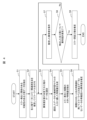
- FIG. 4 is a processing flowchart of the error cause analysis device 3. Below, the details of the error cause analysis process by the error cause analysis device 3 will be explained with reference to FIG. 3 and FIG. 4 as appropriate.
- step S1 the process-specific data extraction unit 31 acquires from the database 2 a data set measured by the semiconductor inspection device 1 using a recipe for which an error cause is to be analyzed, and divides the data by operation process.
- an identification number is given to the data set collected in the database 2 to distinguish which operation process the data was measured in, so that the data set can be divided into measurement data by operation process using this identification number.
- Operation steps that may be related to this error can be, for example, data on the operation step where the error was detected and its upstream operation steps, a series of operation steps that repeat addressing and length measurement, operation steps with close measurement timing, etc.
- Step S2 the error label assignment unit 32 assigns an error label to the measurement point where an error was detected for the process data extracted in step S1, and also assigns error labels to related measurement points (error-related measurement points) that are estimated to affect the inspection performance of this measurement point.
- FIG. 5 is a diagram showing excerpts of process P1 data and process P5 data constituting a data set measured by the semiconductor inspection device 1.
- the "wafer INDEX" in the first column from the left is an identification number for distinguishing the semiconductor wafer.
- the "measurement No.” in the second column from the left is a serial number indicating which measurement point on the same semiconductor wafer it is.
- the method of estimating the error-related measurement point is, for example, if an error is detected in the measurement item with "measurement No.” "12" of a semiconductor wafer with "wafer INDEX” "XXX001" in the process P5 data, the measurement point with the same "wafer INDEX” as the semiconductor wafer and a younger "measurement No.” (for example, the measurement point with "wafer INDEX” "XXX001” and “measurement No.” "0” or "1” in the process P1 data) is estimated to be the error-related measurement point.
- the error label assignment unit 32 then assigns the error label "1" to the error-related measurement point thus estimated and the error detection measurement point that is its origin, as shown in the figure.
- step S3 the error correlation calculation unit 33 selects one of the process-specific data extracted in step S1 for which the anomaly degree calculation has not been completed (the process P1 data or the process P5 data in the example of FIG. 5) as the target for processing in step S4 and thereafter.
- Step S4 the error correlation calculation unit 33 generates features suitable for input to a machine learning model from the data selected in step S3 (for example, the process P1 data in FIG. 5). To this end, the following process is specifically executed.
- the feature generator 33a calculates the correlation of each feature with respect to the occurrence of an error from the difference in data between measurement points with and without the error labels added in step S2.
- the feature generator 33a uses the process-specific data to be processed to generate features suitable for input to a machine learning model that distinguishes between data with and without error labels.
- the generation of features can use, for example, scaling and statistical processing of measurement data, encoding of categorical variables, creation of composite features by combining multiple data such as interaction features, etc.
- the error classification model learning unit 33b uses as input the features generated by the feature generation unit 33a and the error labels assigned in step S2, and learns an error classification model that classifies data from measurement points with error labels based on the difference in tendency between data from measurement points without error labels.
- This error classification model may be generated using any machine learning algorithm, such as a decision tree-based algorithm such as Random Forest or XGBoost, or a Neural Network.
- the model analysis unit 33c calculates the degree of correlation of the error classification model learned by the error classification model learning unit 33b, indicating the degree to which each input feature quantity influenced the error prediction result, which is the model output. For example, when the error detection model is constructed using an algorithm based on a decision tree, this correlation can be evaluated by the feature importance, which is calculated based on the number of times each feature quantity appears in a branch in the model and the improvement value of the objective function, or the SHAP (Shapley Additive exPlanations) value, which calculates the degree of correlation of the value of each feature quantity with the model output.
- the feature importance which is calculated based on the number of times each feature quantity appears in a branch in the model and the improvement value of the objective function
- SHAP Shape Additive exPlanations
- Step S5 the feature extraction unit 34a extracts the feature having the high correlation calculated in step S4.
- the extraction method may be a method of extracting the top N feature amounts in descending order of correlation, or a method of extracting feature amounts having a correlation equal to or greater than a preset threshold.
- Step S6 the feature-based calculation unit 34b calculates the degree of deviation between the data of the measurement point to which the error label of the feature highly correlated with the error extracted in step S5 is assigned and the data of the measurement point without the error label as the degree of abnormality of the operation process.
- the degree of deviation for example, the Euclidean distance or the Mahalanobis distance can be used.
- Step S7 the abnormality degree storage unit 35 stores the abnormality degree for each operation process calculated in step S6.
- step S8 it is determined whether the processes from step S3 to step S7 have been performed for all the operation process data extracted in step S1. If the requirements are met, the process proceeds to step S9, and if the requirements are not met, the processes from step S3 to step S7 are repeated until the degree of anomaly is calculated for all the operation process data.
- step S9 the abnormal process estimation unit 36 estimates the operation process that caused the error by using the degree of abnormality for each operation process stored in step S7.
- the method for estimating the error causing process can be, for example, the operation process with the highest degree of abnormality, the most upstream operation process with a degree of abnormality equal to or higher than a preset threshold, or an operation process estimated using a machine learning model that has learned the relationship between the feature amount highly correlated with the error correlation, the degree of abnormality for each process, and the causing process.
- the estimation result of the process causing the error in this step is output as abnormal process estimation result D1.
- the abnormal process estimation result D1 is an error analysis result including the degree of abnormality for each operation process stored in the abnormality degree storage unit 35 and the process causing the error estimated by the abnormal process estimation unit 36. These error analysis results are presented to the user via terminal 4, which is a GUI.
- Figure 6 shows an example of how to present the error analysis results to the user.
- the level of abnormality for each operation process is indicated by the length of the bar, and process P2, which is presumed to be the cause of the error by the processing in the flowchart of Figure 4, is shown in a different color (darker color) from the other processes.
- process P5 which is presumed to be the cause of the error by the processing in the flowchart of Figure 4
- process P5 which is presumed to be the cause of the error by the processing in the flowchart of Figure 4
- the error information generated is used as is to estimate the error-related measurement points contained in the data of each preceding operation process.Then, the error-related measurement points are regarded as error data, and the deviation between the error data and other data is calculated as the degree of anomaly for each process.
- the error factor analysis device 3 of the second embodiment is obtained by adding a matching score-based anomaly degree calculation unit 37 and a total anomaly degree calculation unit 38 to the error factor analysis device 3 of the first embodiment. The details of these will be explained below.
- the matching score-based anomaly calculation unit 37 calculates the degree of anomaly between the data of a measurement point to which an error label of the matching score is assigned and the data of a measurement point without an error label for each process data that may be the cause of an error extracted by the process data extraction unit 31.
- This degree of anomaly can be a Z score based on the average value or standard deviation of the original data.
- the matching score-based anomaly degree for each process is stored in the anomaly storage unit 35.
- the overall abnormality degree calculation unit 38 calculates an overall degree of abnormality from each degree of abnormality stored in the abnormality degree storage unit 35.
- a schematic diagram of this overall abnormality degree calculation is shown in Fig. 8.
- the overall abnormality degree for each process is calculated from the feature-based abnormality degree and the matching score-based abnormality degree.
- This calculation method can be, for example, a method of simply adding up both the abnormality degrees for each process, a method of taking the maximum value of both, a method of multiplying each by a preset weight and then adding them up, etc.
- the abnormal process estimation unit 36 uses the overall abnormality degree for each process calculated by the overall abnormality degree calculation unit 38 to estimate the process that caused the error based on the level of the abnormality and a threshold value, as in the first embodiment.
- the terminal 4 which is a GUI, may display only the final overall abnormality degree, or may display both the feature-based abnormality degree and the matching score-based abnormality degree, which are the basis for calculating the overall abnormality degree, together with the overall abnormality degree.
- the process estimated by the abnormal process estimation unit 36 to be the cause of the error is shown in a different color (darker color) from the other processes.
- the estimation method of the error process employed by the abnormal process estimation unit 36 is, for example, to estimate the most upstream process whose abnormality degree exceeds a threshold as the process causing the error, then as in the example of FIG. 8, the most upstream process P1 whose abnormality degree exceeds a threshold may be estimated to be the cause of the error, rather than process P2 whose abnormality degree is the highest.
- the error factor analysis device 3 of the third embodiment is different from that of the first embodiment in that it includes a process-specific error factor estimation unit 39, an error dictionary 3A, and an error factor probability correction unit 3B. The details of these will be explained below in order.
- the process-specific error factor estimation unit 39 searches the error dictionary 3A for items with high similarity using the feature amount, its value, correlation degree, etc. that are highly correlated with the error calculated by the error correlation calculation unit 33, and obtains one or more searched error factors and their similarities for each process as error factor probabilities D2. For example, estimation by collaborative filtering or rank learning can be used as a method for calculating this similarity.
- the error dictionary 3A stores combinations of feature quantities, their values, and correlation degrees, and their error causes in association with each other.
- the method of storing the error features and their causes may be systematized in a table format based on past know-how, or past error data and their error causes may be stored.
- the error factor probability correction unit 3B corrects the process-specific error factor probability D2 calculated by the process-specific error factor estimation unit 39, using the process-specific abnormality degree stored in the abnormality degree storage unit 35.
- a schematic diagram of this correction method is shown in FIG.
- the top three error factors and their error probabilities calculated by the process-specific error factor estimation unit 39 are obtained for each process. These error probabilities are corrected by the degree of abnormality for each process stored in the degree of abnormality storage unit 35, and the error probability with the highest degree of error after correction is obtained together with the process number as the error factor estimation result D3.
- the degree of abnormality value may be normalized by [0.0-1.0] and multiplied by the error probability, or a coefficient may be calculated so that processes with an abnormality degree above a threshold are increased and processes with an abnormality degree above the threshold are decreased, and the coefficient may be multiplied by the error probability.
- the error factor estimation result D3 obtained in this way is presented to the user via terminal 4.
- the estimated probability of the error factor obtained for each process is corrected by the abnormality degree for each process, so that the error factor according to the abnormality degree for each process can be estimated.
- the error factor for each process can be extracted and presented to the user.
- the present disclosure is not limited to the above-described embodiments, and includes various modified examples.
- the above-described embodiments have been described in detail to clearly explain the present disclosure, and it is not necessary to include all of the configurations described.
- a part of an embodiment can be replaced with a configuration of another embodiment.
- a configuration of another embodiment can be added to a configuration of an embodiment.
- a part of the configuration of each embodiment can be added to, deleted from, or replaced with a part of the configuration of another embodiment.
- two methods for calculating the degree of anomaly for each process are used: a feature-based degree of anomaly and a matching score-based degree of anomaly.
- three or more other methods for calculating the degree of anomaly may be used.
- Example 3 a process-specific error factor estimation unit 39, an error dictionary 3A, and an error factor probability correction unit 3B are added to the configuration of Example 1, but these may also be added to the configuration of Example 2.
- the information stored in the error dictionary 3A may include recipe modification suggestions, and the error cause and the recipe modification suggestions may be presented together as information presented to the user in the error cause estimation result D3.
- 100 Information processing system
- 1 Semiconductor inspection device
- 2 Database
- 3 Error factor analysis device
- 31 Process-specific data extraction unit
- 32 Error label assignment unit
- 33 Error correlation calculation unit
- 33a Feature generation unit
- 33b Error classification model learning unit
- 33c Model analysis unit
- 34 Anomaly calculation unit
- 34a Feature extraction unit
- 34b Anomaly calculation unit
- 35 Anomaly storage unit
- 36 Abnormal process estimation unit
- 37 Matching score-based anomaly calculation unit
- 38 Overall anomaly calculation unit
- 39 Process-specific error factor estimation unit
- 3A Error dictionary
- 3B Error factor probability correction unit
- 4 Terminal
- D1 Abnormal process estimation result
- D2 Error factor probability
- D3 Error factor estimation result
- N Network
Landscapes
- Physics & Mathematics (AREA)
- Engineering & Computer Science (AREA)
- General Physics & Mathematics (AREA)
- Automation & Control Theory (AREA)
- Artificial Intelligence (AREA)
- Evolutionary Computation (AREA)
- Mathematical Physics (AREA)
- Testing Or Measuring Of Semiconductors Or The Like (AREA)
- Debugging And Monitoring (AREA)
- Testing And Monitoring For Control Systems (AREA)
Priority Applications (5)
| Application Number | Priority Date | Filing Date | Title |
|---|---|---|---|
| JP2024558565A JP7821323B2 (ja) | 2022-11-16 | 2022-11-16 | エラー要因解析装置、および、エラー要因解析方法 |
| KR1020257013407A KR20250076593A (ko) | 2022-11-16 | 2022-11-16 | 에러 요인 해석 장치, 및 에러 요인 해석 방법 |
| PCT/JP2022/042563 WO2024105811A1 (ja) | 2022-11-16 | 2022-11-16 | エラー要因解析装置、および、エラー要因解析方法 |
| CN202280101550.5A CN120153466A (zh) | 2022-11-16 | 2022-11-16 | 错误因素解析装置以及错误因素解析方法 |
| TW112141453A TWI863659B (zh) | 2022-11-16 | 2023-10-30 | 錯誤因素解析裝置及錯誤因素解析方法 |
Applications Claiming Priority (1)
| Application Number | Priority Date | Filing Date | Title |
|---|---|---|---|
| PCT/JP2022/042563 WO2024105811A1 (ja) | 2022-11-16 | 2022-11-16 | エラー要因解析装置、および、エラー要因解析方法 |
Publications (1)
| Publication Number | Publication Date |
|---|---|
| WO2024105811A1 true WO2024105811A1 (ja) | 2024-05-23 |
Family
ID=91084051
Family Applications (1)
| Application Number | Title | Priority Date | Filing Date |
|---|---|---|---|
| PCT/JP2022/042563 Ceased WO2024105811A1 (ja) | 2022-11-16 | 2022-11-16 | エラー要因解析装置、および、エラー要因解析方法 |
Country Status (5)
| Country | Link |
|---|---|
| JP (1) | JP7821323B2 (https=) |
| KR (1) | KR20250076593A (https=) |
| CN (1) | CN120153466A (https=) |
| TW (1) | TWI863659B (https=) |
| WO (1) | WO2024105811A1 (https=) |
Citations (3)
| Publication number | Priority date | Publication date | Assignee | Title |
|---|---|---|---|---|
| JP2019054179A (ja) * | 2017-09-19 | 2019-04-04 | パナソニックIpマネジメント株式会社 | エラー要因推定装置およびエラー要因推定方法 |
| WO2021044611A1 (ja) * | 2019-09-06 | 2021-03-11 | 株式会社日立ハイテク | レシピ情報提示システム、レシピエラー推定システム |
| WO2021199164A1 (ja) * | 2020-03-30 | 2021-10-07 | 株式会社日立ハイテク | 診断システム |
Family Cites Families (5)
| Publication number | Priority date | Publication date | Assignee | Title |
|---|---|---|---|---|
| JP4661371B2 (ja) | 2005-06-02 | 2011-03-30 | オムロン株式会社 | 基板検査システム |
| US8838413B2 (en) * | 2011-05-12 | 2014-09-16 | Saudi Arabian Oil Company | Valve actuator fault analysis system |
| KR101965839B1 (ko) * | 2017-08-18 | 2019-04-05 | 주식회사 티맥스 소프트 | 구성정보 관리 데이터베이스 기반의 it 시스템 장애 분석 기법 |
| WO2021053738A1 (ja) * | 2019-09-18 | 2021-03-25 | 三菱電機株式会社 | 作業要素分析装置及び作業要素分析方法 |
| WO2022059183A1 (ja) * | 2020-09-18 | 2022-03-24 | 三菱電機株式会社 | 情報処理装置、情報処理方法及び情報処理プログラム |
-
2022
- 2022-11-16 WO PCT/JP2022/042563 patent/WO2024105811A1/ja not_active Ceased
- 2022-11-16 KR KR1020257013407A patent/KR20250076593A/ko active Pending
- 2022-11-16 JP JP2024558565A patent/JP7821323B2/ja active Active
- 2022-11-16 CN CN202280101550.5A patent/CN120153466A/zh active Pending
-
2023
- 2023-10-30 TW TW112141453A patent/TWI863659B/zh active
Patent Citations (3)
| Publication number | Priority date | Publication date | Assignee | Title |
|---|---|---|---|---|
| JP2019054179A (ja) * | 2017-09-19 | 2019-04-04 | パナソニックIpマネジメント株式会社 | エラー要因推定装置およびエラー要因推定方法 |
| WO2021044611A1 (ja) * | 2019-09-06 | 2021-03-11 | 株式会社日立ハイテク | レシピ情報提示システム、レシピエラー推定システム |
| WO2021199164A1 (ja) * | 2020-03-30 | 2021-10-07 | 株式会社日立ハイテク | 診断システム |
Also Published As
| Publication number | Publication date |
|---|---|
| TWI863659B (zh) | 2024-11-21 |
| CN120153466A (zh) | 2025-06-13 |
| KR20250076593A (ko) | 2025-05-29 |
| TW202422258A (zh) | 2024-06-01 |
| JP7821323B2 (ja) | 2026-02-26 |
| JPWO2024105811A1 (https=) | 2024-05-23 |
Similar Documents
| Publication | Publication Date | Title |
|---|---|---|
| US12554571B2 (en) | Error cause estimation device and estimation method | |
| CN116188475A (zh) | 一种外观缺陷自动光学检测的智慧控制方法、系统及介质 | |
| CN117358615B (zh) | 一种自动喷码印刷缺陷检测方法及系统 | |
| JP2000057349A (ja) | 欠陥の分類方法およびその装置並びに教示用データ作成方法 | |
| TWI801973B (zh) | 錯誤因素之推定裝置及推定方法 | |
| WO2020166236A1 (ja) | 作業効率評価方法、作業効率評価装置、及びプログラム | |
| CN109285791B (zh) | 设计布局为主的快速在线缺陷诊断、分类及取样方法及系统 | |
| JP2009068946A (ja) | 欠陥分類装置および方法並びにプログラム | |
| KR20210122429A (ko) | 영상 딥러닝을 이용한 ai 기반 화장품 용기 인쇄 제조 공정에서의 자동 결함 탐지 방법 및 시스템 | |
| CN112529109A (zh) | 一种基于无监督多模型的异常检测方法及系统 | |
| TW202028901A (zh) | 異常因子推估裝置、異常因子推估方法及程式產品 | |
| JP5298552B2 (ja) | 判別装置、判別方法及びプログラム | |
| JP7610028B2 (ja) | エラー要因推定装置、エラー要因推定方法及びコンピュータ可読媒体 | |
| JP2006318263A (ja) | 情報分析システム、情報分析方法及びプログラム | |
| JP2022113099A (ja) | 作業管理装置、作業管理方法、および作業管理プログラム | |
| JP7821323B2 (ja) | エラー要因解析装置、および、エラー要因解析方法 | |
| JP4758619B2 (ja) | 問題工程特定方法および装置 | |
| CN119816917A (zh) | 信息处理方法、计算机程序以及信息处理装置 | |
| CN117671376B (zh) | 一种环形缺陷的识别方法及系统 | |
| CN117690817B (zh) | 一种直线缺陷的识别方法及系统 | |
| CN116894965A (zh) | 教师数据收集方法以及收集装置 | |
| Jain et al. | 3 Fault Detection in | |
| CN121350505A (zh) | 基于图像处理的品控管理智能检验方法、系统及介质 | |
| WO2022158216A1 (ja) | 作業管理装置、作業管理方法、および作業管理プログラム | |
| CN120124726A (zh) | 一种异常检测排查方法及系统 |
Legal Events
| Date | Code | Title | Description |
|---|---|---|---|
| 121 | Ep: the epo has been informed by wipo that ep was designated in this application |
Ref document number: 22965787 Country of ref document: EP Kind code of ref document: A1 |
|
| WWE | Wipo information: entry into national phase |
Ref document number: 2024558565 Country of ref document: JP |
|
| ENP | Entry into the national phase |
Ref document number: 20257013407 Country of ref document: KR Kind code of ref document: A |
|
| WWE | Wipo information: entry into national phase |
Ref document number: 1020257013407 Country of ref document: KR |
|
| WWE | Wipo information: entry into national phase |
Ref document number: 202280101550.5 Country of ref document: CN |
|
| WWP | Wipo information: published in national office |
Ref document number: 202280101550.5 Country of ref document: CN |
|
| NENP | Non-entry into the national phase |
Ref country code: DE |
|
| 122 | Ep: pct application non-entry in european phase |
Ref document number: 22965787 Country of ref document: EP Kind code of ref document: A1 |