WO2024090348A1 - 伸縮性デバイス - Google Patents
伸縮性デバイス Download PDFInfo
- Publication number
- WO2024090348A1 WO2024090348A1 PCT/JP2023/037997 JP2023037997W WO2024090348A1 WO 2024090348 A1 WO2024090348 A1 WO 2024090348A1 JP 2023037997 W JP2023037997 W JP 2023037997W WO 2024090348 A1 WO2024090348 A1 WO 2024090348A1
- Authority
- WO
- WIPO (PCT)
- Prior art keywords
- stretchable
- conductive
- stretchable device
- conductive portion
- plan
- Prior art date
- Legal status (The legal status is an assumption and is not a legal conclusion. Google has not performed a legal analysis and makes no representation as to the accuracy of the status listed.)
- Ceased
Links
Images


Classifications
-
- H—ELECTRICITY
- H05—ELECTRIC TECHNIQUES NOT OTHERWISE PROVIDED FOR
- H05K—PRINTED CIRCUITS; CASINGS OR CONSTRUCTIONAL DETAILS OF ELECTRIC APPARATUS; MANUFACTURE OF ASSEMBLAGES OF ELECTRICAL COMPONENTS
- H05K1/00—Printed circuits
- H05K1/02—Details
-
- H—ELECTRICITY
- H05—ELECTRIC TECHNIQUES NOT OTHERWISE PROVIDED FOR
- H05K—PRINTED CIRCUITS; CASINGS OR CONSTRUCTIONAL DETAILS OF ELECTRIC APPARATUS; MANUFACTURE OF ASSEMBLAGES OF ELECTRICAL COMPONENTS
- H05K1/00—Printed circuits
- H05K1/16—Printed circuits incorporating printed electric components, e.g. printed resistors, capacitors or inductors
Definitions
- the present invention relates to a stretchable device.
- Stretchable devices in which stretchable wiring is provided on a stretchable substrate have been known for some time. These stretchable devices can be attached to a living body and used (see Patent Document 1).
- stretchable wirings with different stretchability i.e., stretchable conductive parts
- stretchable conductive parts may be provided on the stretchable substrate.
- the two conductive parts are both made of a material that contains silver or the like, the resistivity of the conductive part as a whole may become high.
- the present invention aims to provide a stretchable device with a conductive part that can optimally ensure a predetermined stretchability and reduce resistance.
- a stretchable substrate A stretchable device is provided, the stretchable device including a plurality of first conductive portions that are spaced apart from one another and are flexible and are provided on the stretchable substrate, and a second conductive portion that is in contact with a portion of the first conductive portion and is stretchable.
- the conductive parts of the stretchable device can be made to have a desired degree of stretchability and low resistance.
- FIG. 1 is a plan view illustrating a stretchable device according to a first embodiment of the present invention.
- FIG. 2A is a plan view illustrating a first-layer stretchable device according to a second embodiment of the present invention.
- FIG. 2B is a plan view illustrating a second-layer stretchable device according to a second embodiment of the present invention.
- FIG. 2C is a plan view illustrating a stacked stretchable device according to a second embodiment of the present invention.
- FIG. 3 is a plan view illustrating a stretchable device according to a third embodiment of the present invention.
- FIG. 4 is a plan view illustrating a stretchable device according to a fourth embodiment of the present invention.
- FIG. 1 is a plan view illustrating a stretchable device according to a first embodiment of the present invention.
- FIG. 2A is a plan view illustrating a first-layer stretchable device according to a second embodiment of the present invention.
- FIG. 2B is a plan view illustrating a second-
- FIG. 5 is a plan view illustrating a stretchable device according to a fifth embodiment of the present invention.
- FIG. 6 is a plan view that illustrates a conventional stretchable device in which the entire first conductive portion is covered with the second conductive portion.
- FIG. 7 is a plan view diagrammatically illustrating a stretchable device comparable to the stretchable device of the first embodiment.
- FIG. 8A is a plan view illustrating a first-layer stretchable device that can be compared to the stretchable device of the second embodiment.
- FIG. 8B is a plan view illustrating a second-layer stretchable device that can be compared to the stretchable device of the second embodiment.
- FIG. 8C is a plan view illustrating a stacked stretchable device that can be compared to the stretchable device of the second embodiment.
- FIG. 9 is a plan view diagrammatically illustrating a stretchable device comparable to the stretchable device of the third embodiment.
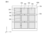
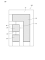
- FIG. 1 is a plan view showing a schematic diagram of a stretchable device according to a first embodiment of the present invention.
- the stretchable device 100 includes a stretchable substrate 10 and different types of conductive parts (first conductive part 20 and second conductive part 30) provided on the stretchable substrate 10.
- the first conductive part 20 is flexible and is provided in a plurality of parts spaced apart from each other.
- the second conductive part 30 is in contact with a part of the first conductive part 20 and is flexible and stretchable.
- the first conductive part 20 may have relatively smaller stretchability than the second conductive part 30.
- the second conductive part 30 may have relatively greater stretchability than the first conductive part 20.
- the term "above” as used in this specification includes a state where it is located above an element and away from it, i.e., above an element via another object, a state where it is located above an element with a gap, and a state where it is located directly above an element. Also, in this drawing, at the partial contact point between the first conductive part 20 and the second conductive part 30, a part of the first conductive part 20 that may be located in the lower layer is shown by a dotted line.
- the stretchable substrate 10 is a sheet-like or film-like stretchable substrate, and is made of, for example, a resin material having stretchability.
- resin materials for the stretchable substrate 10 include thermoplastic polyurethane (TPU), polyethylene (PE), polystyrene (PS), polyethylene terephthalate (PET), etc.
- the thickness of the stretchable substrate 10 is not particularly limited, but from the viewpoint of not inhibiting the stretching of the surface of the living body when attached to the living body, it is preferably 100 ⁇ m or less, and more preferably 50 ⁇ m or less. In addition, from the viewpoint of ensuring a certain strength, the thickness of the stretchable substrate 10 is preferably 20 ⁇ m or more.
- the first conductive part 20 may be a metal foil.
- copper may be used as the metal foil.
- the first conductive part 20 may have a block shape, for example, a rectangular shape, in a plan view.
- the second conductive part 30 may include a resin and a particulate conductive material dispersed in the resin.
- the second conductive part 30 may be a mixture of a metal powder such as Ag as a conductive material, or a non-metal powder such as a carbon-based powder, and an elastomer-based resin such as a silicone resin.
- the average particle size of the conductive material is not particularly limited, but is preferably 0.01 ⁇ m or more and 10 ⁇ m or less.
- the conductive material is preferably spherical in shape.
- the thickness of the first conductive section 20 and the second conductive section 30 is not particularly limited, but is preferably 100 ⁇ m or less, and more preferably 50 ⁇ m or less. In addition, the thickness of these conductive sections is preferably 0.1 ⁇ m or more.
- one of the two conductive parts, the second conductive part 30, has elasticity, while the first conductive part 20 does not have elasticity.
- the resistivity of the conductive part as a whole can be made lower, and low resistance can be achieved.
- a configuration may be adopted in which the second conductive portion 30" (corresponding to the second conductive portion 30 described above) continuously covers the substrate 10" (corresponding to the stretchable substrate 10 described above) and the first conductive portion 20" (corresponding to the first conductive portion 20 described above).
- the entire first conductive portion 20" and the second conductive portion 30" may overlap each other.
- there is a risk that the stretchability of the second conductive portion 30" may be impaired due to a difference in the degree (magnitude) of stretchability between the second conductive portion 30" and the first conductive portion 20".
- the first conductive section 20 due to contact between a part of the first conductive section 20 and the second conductive section 30, the first conductive section 20, specifically a part of the first conductive section 20, may be exposed without the first conductive section 20 and the second conductive section 30 overlapping in a plan view.
- the second conductive section 30 may be configured to cover the substrate 10 located between the first conductive sections 20 that are spaced apart from each other, rather than continuously covering the substrate 10 and the first conductive section 20. That is, in a plan view, the second conductive section 30 may have a form in which the stretchable substrate 10 and the first conductive section 20 are discontinuously covered.
- "partial exposure of the first conductive section 20" means exposure from the second conductive section 30, and other components such as an insulating layer may be disposed on the first conductive section 20.
- the second conductive part 30 can be efficiently positioned at the location where elasticity is desired, and as a result, the elasticity of the second conductive part 30 can be prevented from being hindered due to differences in the degree of elasticity between the second conductive part 30 and the first conductive part 20. This makes it possible to preferably ensure a predetermined elasticity of the second conductive part 30.
- the stretchable device 100 of the first embodiment it is possible to preferably ensure a predetermined stretchability and reduce resistance by using the two conductive parts (first conductive part 20, second conductive part 30) of the component parts.
- the first conductive parts 20 are arranged at a predetermined distance apart in the vertical and horizontal directions, and the second conductive parts 30 or the stretchable substrate 10 are arranged so as to connect adjacent first conductive parts 20 in a plan view.
- the elastic region 50 which includes at least one of the elastic substrate 10 and the second conductive section 30, extends continuously in a cross direction that crosses the stretch direction of these elastic members.
- the "stretch direction” refers to the main stretch direction of the elastic member.
- the stretchable region 50 shown in FIG. 1 comprises, for example, a second conductive section 30, a stretchable substrate 10, and a second conductive section 30 that are continuous with each other, and extend continuously in a longitudinal direction perpendicular to the stretching direction indicated by the arrow.
- the stretchable region 50 includes a non-overlapping region where the first conductive section 20 and the second conductive section 30 do not overlap, and preferably most of the stretchable region 50 can be the non-overlapping region.
- the proportion of the non-overlapping region in the stretchable region 50 can be approximately 90% or more. This makes it difficult for the stretching action of the stretchable member to be hindered.
- the stretchable region is described based on a form in which it can extend continuously in the X direction, but this is not limited thereto, and the stretching action of the stretchable member is also unlikely to be hindered in a form in which it can extend continuously in the Y direction.
- first conductive portion 20 and the second conductive portion 30 provided on the elastic substrate 10 are in partial contact with each other, steps are unlikely to occur in these conductive portions as a whole. This makes it possible to suppress the occurrence of discomfort when the device is applied to the human body.
- the stretchable device 100 of this embodiment can further include electronic components, for example by forming a component mounting land on the first conductive section 20.
- the first conductive section 20 is made of metal foil and has a relatively lower resistance than the stretchable second conductive section 30, so that electronic components that may have a large current density around the terminal can be suitably mounted. Examples of electronic components include sensors, coils, oscillators, etc.
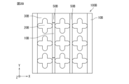
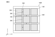
- the configuration of the stretchable device according to the second embodiment will be described below with reference to Figures 2A to 2C.
- the second embodiment is different from the first embodiment (see Figure 1) in that a plurality of stretchable devices are stacked, and in the stacking direction, the stretchable region in the Xth layer (X: natural number, the same applies below) overlaps with the stretchable region in the X+1th layer.
- FIG. 2A is a plan view showing a first layer stretchable device according to a second embodiment of the present invention.
- FIG. 2B is a plan view showing a second layer stretchable device according to a second embodiment of the present invention.
- FIG. 2C is a plan view showing a stacked stretchable device according to a second embodiment of the present invention.
- the stacked stretchable device of Figure 2C (which may also be referred to as a multi-layer stretchable device) is obtained by stacking the stretchable device shown in Figure 2A and the stretchable device shown in Figure 2B along the stacking direction.
- the stretchable region 50A in the Y direction, is composed of a mutually continuous stretchable substrate 10A and a second conductive portion 30A, and extends continuously in the longitudinal direction perpendicular to the stretch direction indicated by the arrow. Also, in the X direction, the stretchable region 50A may be composed of a stretchable substrate 10A extending in one direction. On the other hand, in FIG. 2B, in the Y direction, the stretchable region 50A is composed of a stretchable substrate 10B extending in one direction, and extends continuously in the longitudinal direction perpendicular to the stretch direction indicated by the arrow.
- the above-mentioned stretchable region 50A in the first layer and the above-mentioned stretchable region 50B in the second layer are arranged to overlap each other, and a stretchable laminated region 50C can be formed.
- the elastic laminated region 50C which is composed of the elastic region 50A and the elastic region 50B, extends continuously as a whole in a laminated direction that intersects with the elastic direction of the elastic member (elastic substrate and/or second conductive portion).
- the stretchable laminate region 50X is mostly non-overlapping regions where the first conductive portion 20A and the second conductive portion 30A do not overlap in a plan view, so the stretching action of the stretchable member is less likely to be hindered.
- multiple stretchable regions 50A, 50B are provided, and each of the multiple stretchable regions 50A, 50B is arranged in parallel and spaced apart.
- the multiple stretchable regions can be arranged in parallel with the first conductive portions 20A, 20B in between.
- the stretchable regions 50A and the first conductive portions 20A may be arranged alternately along the stretching direction indicated by the arrow. Furthermore, for example, the stretchable regions 50A extending in the X direction and the stretchable regions 50A extending in the Y direction may cross each other, and the multiple stretchable regions 50A may form a lattice pattern as a whole.
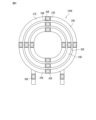
- the third embodiment is different from the first embodiment (see Fig. 1) in that the second conductive part has a meandering shape in a plan view.
- FIG. 3 is a plan view showing a schematic diagram of a stretchable device according to a third embodiment of the present invention.
- the second conductive portion 30C has a serpentine shape in a planar view.
- the resistance R of the second conductive portion is expressed by the following formula 1, where ⁇ is the resistivity, W is the width, t is the thickness, and l is the length.
- the resistance R may become large because the width w is not sufficiently large. Furthermore, when the second conductive portion 30C' is stretched in the direction of the arrow shown in FIG. 9, the resistance of the second conductive portion 30C' increases as it is stretched, and the resistance of the entire conductive portion may also increase.
- the second conductive portion 30C has a meandering shape in plan view, so the overall total width can be increased. This makes it possible to suppress an increase in resistance compared to a shape in which the second conductive portion 30C' extends in one direction between the first conductive portions 20C' (see FIG. 9).
- regions a, e, and f in the second conductive portion 30C located between them will expand, while regions c and h may contract, so that regions of increased width and regions of decreased width may coexist in the second conductive portion.
- an increase in the resistance of the second conductive portion 30 as a whole may be suppressed.
- regions b and d in the second conductive part 30C may expand while regions i and g may contract, so that regions of increased width and regions of decreased width may coexist in the second conductive part.
- an increase in the resistance of the second conductive part 30 as a whole may be suppressed.
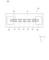
- the fourth embodiment is different from the first embodiment (see Fig. 1) in that it further includes meandering wiring that connects a plurality of first conductive parts together in a plan view.
- FIG. 4 is a plan view showing a schematic diagram of a stretchable device according to a fourth embodiment of the present invention.
- the fourth embodiment further includes meandering wiring that connects multiple first conductive parts together in a planar view.
- the fifth embodiment is different from the first embodiment (see Fig. 1) in that a plurality of stretchable devices are arranged in the stacking direction, and the first conductive part has a coil shape in a plan view.
- FIG. 5 is a plan view showing a schematic diagram of a stretchable device according to a fifth embodiment of the present invention.
- This embodiment is characterized in that multiple stretchable devices are arranged in the stacking direction, and the first conductive part 20E has a coil shape in a plan view.
- the first conductive part 20E has a coil shape in a plan view.
- one first conductive part 21E and the other first conductive part 22E that are adjacent and spaced apart from each other are connected via a stretchable second conductive part 30E.
- the stretchable region 50E in the first layer and the stretchable region 50E in the second layer are arranged to overlap each other, forming a stretchable stacked region.
- this elastic laminated region extends as a whole, via the connection vias, so as to be continuous in a lamination direction that intersects with the elastic direction of the elastic member (elastic substrate and/or second conductive portion).
- the first conductive portion 20E is not present within the elastic laminated region in a plan view, so the elasticity of the elastic member is less likely to be hindered.
- the aspects of the stretchable device according to one embodiment of the present invention are as follows.
- a stretchable substrate A stretchable device comprising: a plurality of first conductive portions that are spaced apart from each other and are flexible, and are provided on the stretchable substrate; and a second conductive portion that is in contact with a portion of the first conductive portion and has stretchability.
- a stretchable device according to ⁇ 1> wherein a portion of the first conductive part is exposed in a planar view.
- ⁇ 3> The stretchable device according to ⁇ 1> or ⁇ 2>, wherein the second conductive part is discontinuous.
- the stretchable region comprising at least one of the stretchable substrate and the second conductive part extends continuously in a cross direction intersecting with the stretching direction.
- the stretchable device according to any one of ⁇ 1> to ⁇ 3>.
- ⁇ 5> The stretchable device according to ⁇ 4>, wherein the stretchable region includes a non-overlapping region where the first conductive portion and the second conductive portion do not overlap in a planar view.
- ⁇ 6> The stretchable device according to ⁇ 4> or ⁇ 5>, wherein the cross direction is a direction perpendicular to the stretch direction.
- ⁇ 7> The stretchable device according to any one of ⁇ 4> to ⁇ 6>, wherein the intersecting direction is a longitudinal extension direction of the stretchable region in a planar view.
- ⁇ 8> The stretchable device according to any one of ⁇ 4> to ⁇ 7>, wherein there are a plurality of the stretchable regions, and the plurality of stretchable regions are arranged in parallel and spaced apart.
- ⁇ 9> The stretchable device according to any one of ⁇ 4> to ⁇ 8>, wherein the stretchable regions and the first conductive parts are alternately arranged along the stretching direction in a planar view.
- ⁇ 10> The stretchable device according to any one of ⁇ 4> to ⁇ 9>, wherein there are a plurality of the stretchable regions, and the plurality of stretchable regions intersect with each other.
- ⁇ 11> The stretchable device according to any one of ⁇ 4> to ⁇ 10>, wherein the stretchable region is a plurality of stretchable regions, and the plurality of stretchable regions form a lattice pattern.
- ⁇ 12> The stretchable device according to any one of ⁇ 4> to ⁇ 11>, wherein a plurality of the stretchable devices are arranged in a stacking direction, and the intersecting direction is the stacking direction.
- ⁇ 13> In the stacking direction, the stretchable region in the Xth layer (X: natural number, the same hereinafter) and the stretchable region in the X+1th layer overlap.
- ⁇ 14> The stretchable device according to any one of ⁇ 1> to ⁇ 13>, wherein the second conductive portion has a meandering shape in a planar view.
- ⁇ 15> The stretchable device according to any one of ⁇ 1> to ⁇ 14>, further comprising meandering wiring connecting the plurality of first conductive parts to each other.
- ⁇ 16> The stretchable device according to any one of ⁇ 1> to ⁇ 5>, wherein a plurality of the first conductive parts are arranged in the stacking direction, and the first conductive parts have a coil shape in a planar view.
- ⁇ 17> The stretchable device according to any one of ⁇ 1> to ⁇ 16>, wherein the first conductive portion has relatively smaller stretchability than the second conductive portion.
- ⁇ 18> The stretchable device according to any one of ⁇ 1> to ⁇ 17>, wherein the first conductive part is a metal foil.
- a constituent material of the first conductive part is copper.
- a constituent material of the second conductive part includes a resin and a conductive member, and the conductive member is at least one selected from silver and carbon-based materials.
Landscapes
- Engineering & Computer Science (AREA)
- Microelectronics & Electronic Packaging (AREA)
- Structure Of Printed Boards (AREA)
Priority Applications (1)
| Application Number | Priority Date | Filing Date | Title |
|---|---|---|---|
| JP2024553023A JPWO2024090348A1 (https=) | 2022-10-24 | 2023-10-20 |
Applications Claiming Priority (2)
| Application Number | Priority Date | Filing Date | Title |
|---|---|---|---|
| JP2022-170040 | 2022-10-24 | ||
| JP2022170040 | 2022-10-24 |
Publications (1)
| Publication Number | Publication Date |
|---|---|
| WO2024090348A1 true WO2024090348A1 (ja) | 2024-05-02 |
Family
ID=90830834
Family Applications (1)
| Application Number | Title | Priority Date | Filing Date |
|---|---|---|---|
| PCT/JP2023/037997 Ceased WO2024090348A1 (ja) | 2022-10-24 | 2023-10-20 | 伸縮性デバイス |
Country Status (2)
| Country | Link |
|---|---|
| JP (1) | JPWO2024090348A1 (https=) |
| WO (1) | WO2024090348A1 (https=) |
Citations (3)
| Publication number | Priority date | Publication date | Assignee | Title |
|---|---|---|---|---|
| WO2020196745A1 (ja) * | 2019-03-27 | 2020-10-01 | パナソニックIpマネジメント株式会社 | 伸縮性回路基板 |
| WO2020217784A1 (ja) * | 2019-04-26 | 2020-10-29 | 株式会社ジャパンディスプレイ | フレキシブル基板 |
| WO2021149321A1 (ja) * | 2020-01-21 | 2021-07-29 | 株式会社ジャパンディスプレイ | フレキシブル基板 |
-
2023
- 2023-10-20 WO PCT/JP2023/037997 patent/WO2024090348A1/ja not_active Ceased
- 2023-10-20 JP JP2024553023A patent/JPWO2024090348A1/ja active Pending
Patent Citations (3)
| Publication number | Priority date | Publication date | Assignee | Title |
|---|---|---|---|---|
| WO2020196745A1 (ja) * | 2019-03-27 | 2020-10-01 | パナソニックIpマネジメント株式会社 | 伸縮性回路基板 |
| WO2020217784A1 (ja) * | 2019-04-26 | 2020-10-29 | 株式会社ジャパンディスプレイ | フレキシブル基板 |
| WO2021149321A1 (ja) * | 2020-01-21 | 2021-07-29 | 株式会社ジャパンディスプレイ | フレキシブル基板 |
Also Published As
| Publication number | Publication date |
|---|---|
| JPWO2024090348A1 (https=) | 2024-05-02 |
Similar Documents
| Publication | Publication Date | Title |
|---|---|---|
| JP6958525B2 (ja) | インダクタ部品 | |
| TW201002194A (en) | Electromagnetic bandgap structure and printed circuit board | |
| CN105636335B (zh) | 移动终端、柔性电路板及其制造方法 | |
| JP2012235080A5 (https=) | ||
| WO2006099297A2 (en) | Conditioner with coplanar conductors | |
| JP6272173B2 (ja) | 配線基板 | |
| CN1393892A (zh) | 多层电感器 | |
| CN210112367U (zh) | 一种覆晶薄膜基板、电路板及显示设备 | |
| WO2018221131A1 (ja) | 電子部品 | |
| JP2013135172A (ja) | プリント配線板及びプリント配線板の接続構造 | |
| US12185458B2 (en) | Flexible wiring board | |
| WO2024090348A1 (ja) | 伸縮性デバイス | |
| CN105636351A (zh) | 柔性线路板及移动终端 | |
| CN117594338A (zh) | 线圈部件 | |
| CN119318210A (zh) | 伸缩性器件 | |
| WO2023106055A1 (ja) | 伸縮性デバイス | |
| JP2001015643A5 (https=) | ||
| CN111149177B (zh) | 电感器及其制造方法 | |
| CN204887687U (zh) | 一种柔性电路板及电子产品 | |
| US20190107905A1 (en) | Touch panel | |
| JP6048719B2 (ja) | プリント配線板及び該プリント配線板の製造方法 | |
| US20170084559A1 (en) | Semiconductor devices with redistribution pads | |
| JP7380048B2 (ja) | フレキシブルプリント配線板アレイおよびその製造方法 | |
| TWM536407U (zh) | 柔性扁平排線 | |
| CN110012594A (zh) | 一种柔性电路板及终端设备 |
Legal Events
| Date | Code | Title | Description |
|---|---|---|---|
| 121 | Ep: the epo has been informed by wipo that ep was designated in this application |
Ref document number: 23882553 Country of ref document: EP Kind code of ref document: A1 |
|
| WWE | Wipo information: entry into national phase |
Ref document number: 2024553023 Country of ref document: JP |
|
| NENP | Non-entry into the national phase |
Ref country code: DE |
|
| 122 | Ep: pct application non-entry in european phase |
Ref document number: 23882553 Country of ref document: EP Kind code of ref document: A1 |