WO2024090348A1 - Stretchable device - Google Patents
Stretchable device Download PDFInfo
- Publication number
- WO2024090348A1 WO2024090348A1 PCT/JP2023/037997 JP2023037997W WO2024090348A1 WO 2024090348 A1 WO2024090348 A1 WO 2024090348A1 JP 2023037997 W JP2023037997 W JP 2023037997W WO 2024090348 A1 WO2024090348 A1 WO 2024090348A1
- Authority
- WO
- WIPO (PCT)
- Prior art keywords
- stretchable
- conductive
- stretchable device
- conductive portion
- plan
- Prior art date
Links
- 239000000463 material Substances 0.000 claims abstract description 8
- 239000000758 substrate Substances 0.000 claims description 34
- 229920005989 resin Polymers 0.000 claims description 7
- 239000011347 resin Substances 0.000 claims description 7
- 229910052751 metal Inorganic materials 0.000 claims description 6
- 239000002184 metal Substances 0.000 claims description 6
- 239000011888 foil Substances 0.000 claims description 5
- 229910052709 silver Inorganic materials 0.000 claims description 4
- 239000004332 silver Substances 0.000 claims description 4
- RYGMFSIKBFXOCR-UHFFFAOYSA-N Copper Chemical compound [Cu] RYGMFSIKBFXOCR-UHFFFAOYSA-N 0.000 claims description 3
- 229910052802 copper Inorganic materials 0.000 claims description 3
- 239000010949 copper Substances 0.000 claims description 3
- 239000003575 carbonaceous material Substances 0.000 claims description 2
- 239000004020 conductor Substances 0.000 description 4
- 238000010586 diagram Methods 0.000 description 4
- 239000000470 constituent Substances 0.000 description 3
- 230000004048 modification Effects 0.000 description 3
- 238000012986 modification Methods 0.000 description 3
- 239000000843 powder Substances 0.000 description 3
- 239000004698 Polyethylene Substances 0.000 description 2
- 239000004433 Thermoplastic polyurethane Substances 0.000 description 2
- 230000003247 decreasing effect Effects 0.000 description 2
- 230000000694 effects Effects 0.000 description 2
- -1 polyethylene Polymers 0.000 description 2
- 229920000573 polyethylene Polymers 0.000 description 2
- 229920000139 polyethylene terephthalate Polymers 0.000 description 2
- 239000005020 polyethylene terephthalate Substances 0.000 description 2
- 229920002803 thermoplastic polyurethane Polymers 0.000 description 2
- OKTJSMMVPCPJKN-UHFFFAOYSA-N Carbon Chemical compound [C] OKTJSMMVPCPJKN-UHFFFAOYSA-N 0.000 description 1
- 239000004793 Polystyrene Substances 0.000 description 1
- 229910052799 carbon Inorganic materials 0.000 description 1
- 229920001971 elastomer Polymers 0.000 description 1
- 239000000806 elastomer Substances 0.000 description 1
- 230000001771 impaired effect Effects 0.000 description 1
- 230000002401 inhibitory effect Effects 0.000 description 1
- 238000003475 lamination Methods 0.000 description 1
- 239000000203 mixture Substances 0.000 description 1
- 229910052755 nonmetal Inorganic materials 0.000 description 1
- 239000002245 particle Substances 0.000 description 1
- 229920002050 silicone resin Polymers 0.000 description 1
- 238000006467 substitution reaction Methods 0.000 description 1
Images


Classifications
-
- H—ELECTRICITY
- H05—ELECTRIC TECHNIQUES NOT OTHERWISE PROVIDED FOR
- H05K—PRINTED CIRCUITS; CASINGS OR CONSTRUCTIONAL DETAILS OF ELECTRIC APPARATUS; MANUFACTURE OF ASSEMBLAGES OF ELECTRICAL COMPONENTS
- H05K1/00—Printed circuits
- H05K1/02—Details
-
- H—ELECTRICITY
- H05—ELECTRIC TECHNIQUES NOT OTHERWISE PROVIDED FOR
- H05K—PRINTED CIRCUITS; CASINGS OR CONSTRUCTIONAL DETAILS OF ELECTRIC APPARATUS; MANUFACTURE OF ASSEMBLAGES OF ELECTRICAL COMPONENTS
- H05K1/00—Printed circuits
- H05K1/16—Printed circuits incorporating printed electric components, e.g. printed resistor, capacitor, inductor
Definitions
- the present invention relates to a stretchable device.
- Stretchable devices in which stretchable wiring is provided on a stretchable substrate have been known for some time. These stretchable devices can be attached to a living body and used (see Patent Document 1).
- stretchable wirings with different stretchability i.e., stretchable conductive parts
- stretchable conductive parts may be provided on the stretchable substrate.
- the two conductive parts are both made of a material that contains silver or the like, the resistivity of the conductive part as a whole may become high.
- the present invention aims to provide a stretchable device with a conductive part that can optimally ensure a predetermined stretchability and reduce resistance.
- a stretchable substrate A stretchable device is provided, the stretchable device including a plurality of first conductive portions that are spaced apart from one another and are flexible and are provided on the stretchable substrate, and a second conductive portion that is in contact with a portion of the first conductive portion and is stretchable.
- the conductive parts of the stretchable device can be made to have a desired degree of stretchability and low resistance.
- FIG. 1 is a plan view illustrating a stretchable device according to a first embodiment of the present invention.
- FIG. 2A is a plan view illustrating a first-layer stretchable device according to a second embodiment of the present invention.
- FIG. 2B is a plan view illustrating a second-layer stretchable device according to a second embodiment of the present invention.
- FIG. 2C is a plan view illustrating a stacked stretchable device according to a second embodiment of the present invention.
- FIG. 3 is a plan view illustrating a stretchable device according to a third embodiment of the present invention.
- FIG. 4 is a plan view illustrating a stretchable device according to a fourth embodiment of the present invention.
- FIG. 1 is a plan view illustrating a stretchable device according to a first embodiment of the present invention.
- FIG. 2A is a plan view illustrating a first-layer stretchable device according to a second embodiment of the present invention.
- FIG. 2B is a plan view illustrating a second-
- FIG. 5 is a plan view illustrating a stretchable device according to a fifth embodiment of the present invention.
- FIG. 6 is a plan view that illustrates a conventional stretchable device in which the entire first conductive portion is covered with the second conductive portion.
- FIG. 7 is a plan view diagrammatically illustrating a stretchable device comparable to the stretchable device of the first embodiment.
- FIG. 8A is a plan view illustrating a first-layer stretchable device that can be compared to the stretchable device of the second embodiment.
- FIG. 8B is a plan view illustrating a second-layer stretchable device that can be compared to the stretchable device of the second embodiment.
- FIG. 8C is a plan view illustrating a stacked stretchable device that can be compared to the stretchable device of the second embodiment.
- FIG. 9 is a plan view diagrammatically illustrating a stretchable device comparable to the stretchable device of the third embodiment.
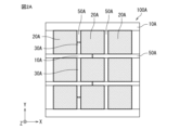
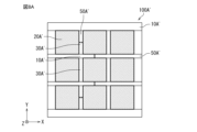
- FIG. 1 is a plan view showing a schematic diagram of a stretchable device according to a first embodiment of the present invention.
- the stretchable device 100 includes a stretchable substrate 10 and different types of conductive parts (first conductive part 20 and second conductive part 30) provided on the stretchable substrate 10.
- the first conductive part 20 is flexible and is provided in a plurality of parts spaced apart from each other.
- the second conductive part 30 is in contact with a part of the first conductive part 20 and is flexible and stretchable.
- the first conductive part 20 may have relatively smaller stretchability than the second conductive part 30.
- the second conductive part 30 may have relatively greater stretchability than the first conductive part 20.
- the term "above” as used in this specification includes a state where it is located above an element and away from it, i.e., above an element via another object, a state where it is located above an element with a gap, and a state where it is located directly above an element. Also, in this drawing, at the partial contact point between the first conductive part 20 and the second conductive part 30, a part of the first conductive part 20 that may be located in the lower layer is shown by a dotted line.
- the stretchable substrate 10 is a sheet-like or film-like stretchable substrate, and is made of, for example, a resin material having stretchability.
- resin materials for the stretchable substrate 10 include thermoplastic polyurethane (TPU), polyethylene (PE), polystyrene (PS), polyethylene terephthalate (PET), etc.
- the thickness of the stretchable substrate 10 is not particularly limited, but from the viewpoint of not inhibiting the stretching of the surface of the living body when attached to the living body, it is preferably 100 ⁇ m or less, and more preferably 50 ⁇ m or less. In addition, from the viewpoint of ensuring a certain strength, the thickness of the stretchable substrate 10 is preferably 20 ⁇ m or more.
- the first conductive part 20 may be a metal foil.
- copper may be used as the metal foil.
- the first conductive part 20 may have a block shape, for example, a rectangular shape, in a plan view.
- the second conductive part 30 may include a resin and a particulate conductive material dispersed in the resin.
- the second conductive part 30 may be a mixture of a metal powder such as Ag as a conductive material, or a non-metal powder such as a carbon-based powder, and an elastomer-based resin such as a silicone resin.
- the average particle size of the conductive material is not particularly limited, but is preferably 0.01 ⁇ m or more and 10 ⁇ m or less.
- the conductive material is preferably spherical in shape.
- the thickness of the first conductive section 20 and the second conductive section 30 is not particularly limited, but is preferably 100 ⁇ m or less, and more preferably 50 ⁇ m or less. In addition, the thickness of these conductive sections is preferably 0.1 ⁇ m or more.
- one of the two conductive parts, the second conductive part 30, has elasticity, while the first conductive part 20 does not have elasticity.
- the resistivity of the conductive part as a whole can be made lower, and low resistance can be achieved.
- a configuration may be adopted in which the second conductive portion 30" (corresponding to the second conductive portion 30 described above) continuously covers the substrate 10" (corresponding to the stretchable substrate 10 described above) and the first conductive portion 20" (corresponding to the first conductive portion 20 described above).
- the entire first conductive portion 20" and the second conductive portion 30" may overlap each other.
- there is a risk that the stretchability of the second conductive portion 30" may be impaired due to a difference in the degree (magnitude) of stretchability between the second conductive portion 30" and the first conductive portion 20".
- the first conductive section 20 due to contact between a part of the first conductive section 20 and the second conductive section 30, the first conductive section 20, specifically a part of the first conductive section 20, may be exposed without the first conductive section 20 and the second conductive section 30 overlapping in a plan view.
- the second conductive section 30 may be configured to cover the substrate 10 located between the first conductive sections 20 that are spaced apart from each other, rather than continuously covering the substrate 10 and the first conductive section 20. That is, in a plan view, the second conductive section 30 may have a form in which the stretchable substrate 10 and the first conductive section 20 are discontinuously covered.
- "partial exposure of the first conductive section 20" means exposure from the second conductive section 30, and other components such as an insulating layer may be disposed on the first conductive section 20.
- the second conductive part 30 can be efficiently positioned at the location where elasticity is desired, and as a result, the elasticity of the second conductive part 30 can be prevented from being hindered due to differences in the degree of elasticity between the second conductive part 30 and the first conductive part 20. This makes it possible to preferably ensure a predetermined elasticity of the second conductive part 30.
- the stretchable device 100 of the first embodiment it is possible to preferably ensure a predetermined stretchability and reduce resistance by using the two conductive parts (first conductive part 20, second conductive part 30) of the component parts.
- the first conductive parts 20 are arranged at a predetermined distance apart in the vertical and horizontal directions, and the second conductive parts 30 or the stretchable substrate 10 are arranged so as to connect adjacent first conductive parts 20 in a plan view.
- the elastic region 50 which includes at least one of the elastic substrate 10 and the second conductive section 30, extends continuously in a cross direction that crosses the stretch direction of these elastic members.
- the "stretch direction” refers to the main stretch direction of the elastic member.
- the stretchable region 50 shown in FIG. 1 comprises, for example, a second conductive section 30, a stretchable substrate 10, and a second conductive section 30 that are continuous with each other, and extend continuously in a longitudinal direction perpendicular to the stretching direction indicated by the arrow.
- the stretchable region 50 includes a non-overlapping region where the first conductive section 20 and the second conductive section 30 do not overlap, and preferably most of the stretchable region 50 can be the non-overlapping region.
- the proportion of the non-overlapping region in the stretchable region 50 can be approximately 90% or more. This makes it difficult for the stretching action of the stretchable member to be hindered.
- the stretchable region is described based on a form in which it can extend continuously in the X direction, but this is not limited thereto, and the stretching action of the stretchable member is also unlikely to be hindered in a form in which it can extend continuously in the Y direction.
- first conductive portion 20 and the second conductive portion 30 provided on the elastic substrate 10 are in partial contact with each other, steps are unlikely to occur in these conductive portions as a whole. This makes it possible to suppress the occurrence of discomfort when the device is applied to the human body.
- the stretchable device 100 of this embodiment can further include electronic components, for example by forming a component mounting land on the first conductive section 20.
- the first conductive section 20 is made of metal foil and has a relatively lower resistance than the stretchable second conductive section 30, so that electronic components that may have a large current density around the terminal can be suitably mounted. Examples of electronic components include sensors, coils, oscillators, etc.
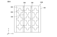
- the configuration of the stretchable device according to the second embodiment will be described below with reference to Figures 2A to 2C.
- the second embodiment is different from the first embodiment (see Figure 1) in that a plurality of stretchable devices are stacked, and in the stacking direction, the stretchable region in the Xth layer (X: natural number, the same applies below) overlaps with the stretchable region in the X+1th layer.
- FIG. 2A is a plan view showing a first layer stretchable device according to a second embodiment of the present invention.
- FIG. 2B is a plan view showing a second layer stretchable device according to a second embodiment of the present invention.
- FIG. 2C is a plan view showing a stacked stretchable device according to a second embodiment of the present invention.
- the stacked stretchable device of Figure 2C (which may also be referred to as a multi-layer stretchable device) is obtained by stacking the stretchable device shown in Figure 2A and the stretchable device shown in Figure 2B along the stacking direction.
- the stretchable region 50A in the Y direction, is composed of a mutually continuous stretchable substrate 10A and a second conductive portion 30A, and extends continuously in the longitudinal direction perpendicular to the stretch direction indicated by the arrow. Also, in the X direction, the stretchable region 50A may be composed of a stretchable substrate 10A extending in one direction. On the other hand, in FIG. 2B, in the Y direction, the stretchable region 50A is composed of a stretchable substrate 10B extending in one direction, and extends continuously in the longitudinal direction perpendicular to the stretch direction indicated by the arrow.
- the above-mentioned stretchable region 50A in the first layer and the above-mentioned stretchable region 50B in the second layer are arranged to overlap each other, and a stretchable laminated region 50C can be formed.
- the elastic laminated region 50C which is composed of the elastic region 50A and the elastic region 50B, extends continuously as a whole in a laminated direction that intersects with the elastic direction of the elastic member (elastic substrate and/or second conductive portion).
- the stretchable laminate region 50X is mostly non-overlapping regions where the first conductive portion 20A and the second conductive portion 30A do not overlap in a plan view, so the stretching action of the stretchable member is less likely to be hindered.
- multiple stretchable regions 50A, 50B are provided, and each of the multiple stretchable regions 50A, 50B is arranged in parallel and spaced apart.
- the multiple stretchable regions can be arranged in parallel with the first conductive portions 20A, 20B in between.
- the stretchable regions 50A and the first conductive portions 20A may be arranged alternately along the stretching direction indicated by the arrow. Furthermore, for example, the stretchable regions 50A extending in the X direction and the stretchable regions 50A extending in the Y direction may cross each other, and the multiple stretchable regions 50A may form a lattice pattern as a whole.
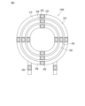
- the third embodiment is different from the first embodiment (see Fig. 1) in that the second conductive part has a meandering shape in a plan view.
- FIG. 3 is a plan view showing a schematic diagram of a stretchable device according to a third embodiment of the present invention.
- the second conductive portion 30C has a serpentine shape in a planar view.
- the resistance R of the second conductive portion is expressed by the following formula 1, where ⁇ is the resistivity, W is the width, t is the thickness, and l is the length.
- the resistance R may become large because the width w is not sufficiently large. Furthermore, when the second conductive portion 30C' is stretched in the direction of the arrow shown in FIG. 9, the resistance of the second conductive portion 30C' increases as it is stretched, and the resistance of the entire conductive portion may also increase.
- the second conductive portion 30C has a meandering shape in plan view, so the overall total width can be increased. This makes it possible to suppress an increase in resistance compared to a shape in which the second conductive portion 30C' extends in one direction between the first conductive portions 20C' (see FIG. 9).
- regions a, e, and f in the second conductive portion 30C located between them will expand, while regions c and h may contract, so that regions of increased width and regions of decreased width may coexist in the second conductive portion.
- an increase in the resistance of the second conductive portion 30 as a whole may be suppressed.
- regions b and d in the second conductive part 30C may expand while regions i and g may contract, so that regions of increased width and regions of decreased width may coexist in the second conductive part.
- an increase in the resistance of the second conductive part 30 as a whole may be suppressed.
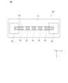
- the fourth embodiment is different from the first embodiment (see Fig. 1) in that it further includes meandering wiring that connects a plurality of first conductive parts together in a plan view.
- FIG. 4 is a plan view showing a schematic diagram of a stretchable device according to a fourth embodiment of the present invention.
- the fourth embodiment further includes meandering wiring that connects multiple first conductive parts together in a planar view.
- the fifth embodiment is different from the first embodiment (see Fig. 1) in that a plurality of stretchable devices are arranged in the stacking direction, and the first conductive part has a coil shape in a plan view.
- FIG. 5 is a plan view showing a schematic diagram of a stretchable device according to a fifth embodiment of the present invention.
- This embodiment is characterized in that multiple stretchable devices are arranged in the stacking direction, and the first conductive part 20E has a coil shape in a plan view.
- the first conductive part 20E has a coil shape in a plan view.
- one first conductive part 21E and the other first conductive part 22E that are adjacent and spaced apart from each other are connected via a stretchable second conductive part 30E.
- the stretchable region 50E in the first layer and the stretchable region 50E in the second layer are arranged to overlap each other, forming a stretchable stacked region.
- this elastic laminated region extends as a whole, via the connection vias, so as to be continuous in a lamination direction that intersects with the elastic direction of the elastic member (elastic substrate and/or second conductive portion).
- the first conductive portion 20E is not present within the elastic laminated region in a plan view, so the elasticity of the elastic member is less likely to be hindered.
- the aspects of the stretchable device according to one embodiment of the present invention are as follows.
- a stretchable substrate A stretchable device comprising: a plurality of first conductive portions that are spaced apart from each other and are flexible, and are provided on the stretchable substrate; and a second conductive portion that is in contact with a portion of the first conductive portion and has stretchability.
- a stretchable device according to ⁇ 1> wherein a portion of the first conductive part is exposed in a planar view.
- ⁇ 3> The stretchable device according to ⁇ 1> or ⁇ 2>, wherein the second conductive part is discontinuous.
- the stretchable region comprising at least one of the stretchable substrate and the second conductive part extends continuously in a cross direction intersecting with the stretching direction.
- the stretchable device according to any one of ⁇ 1> to ⁇ 3>.
- ⁇ 5> The stretchable device according to ⁇ 4>, wherein the stretchable region includes a non-overlapping region where the first conductive portion and the second conductive portion do not overlap in a planar view.
- ⁇ 6> The stretchable device according to ⁇ 4> or ⁇ 5>, wherein the cross direction is a direction perpendicular to the stretch direction.
- ⁇ 7> The stretchable device according to any one of ⁇ 4> to ⁇ 6>, wherein the intersecting direction is a longitudinal extension direction of the stretchable region in a planar view.
- ⁇ 8> The stretchable device according to any one of ⁇ 4> to ⁇ 7>, wherein there are a plurality of the stretchable regions, and the plurality of stretchable regions are arranged in parallel and spaced apart.
- ⁇ 9> The stretchable device according to any one of ⁇ 4> to ⁇ 8>, wherein the stretchable regions and the first conductive parts are alternately arranged along the stretching direction in a planar view.
- ⁇ 10> The stretchable device according to any one of ⁇ 4> to ⁇ 9>, wherein there are a plurality of the stretchable regions, and the plurality of stretchable regions intersect with each other.
- ⁇ 11> The stretchable device according to any one of ⁇ 4> to ⁇ 10>, wherein the stretchable region is a plurality of stretchable regions, and the plurality of stretchable regions form a lattice pattern.
- ⁇ 12> The stretchable device according to any one of ⁇ 4> to ⁇ 11>, wherein a plurality of the stretchable devices are arranged in a stacking direction, and the intersecting direction is the stacking direction.
- ⁇ 13> In the stacking direction, the stretchable region in the Xth layer (X: natural number, the same hereinafter) and the stretchable region in the X+1th layer overlap.
- ⁇ 14> The stretchable device according to any one of ⁇ 1> to ⁇ 13>, wherein the second conductive portion has a meandering shape in a planar view.
- ⁇ 15> The stretchable device according to any one of ⁇ 1> to ⁇ 14>, further comprising meandering wiring connecting the plurality of first conductive parts to each other.
- ⁇ 16> The stretchable device according to any one of ⁇ 1> to ⁇ 5>, wherein a plurality of the first conductive parts are arranged in the stacking direction, and the first conductive parts have a coil shape in a planar view.
- ⁇ 17> The stretchable device according to any one of ⁇ 1> to ⁇ 16>, wherein the first conductive portion has relatively smaller stretchability than the second conductive portion.
- ⁇ 18> The stretchable device according to any one of ⁇ 1> to ⁇ 17>, wherein the first conductive part is a metal foil.
- a constituent material of the first conductive part is copper.
- a constituent material of the second conductive part includes a resin and a conductive member, and the conductive member is at least one selected from silver and carbon-based materials.
Landscapes
- Engineering & Computer Science (AREA)
- Microelectronics & Electronic Packaging (AREA)
- Structure Of Printed Boards (AREA)
Abstract
One embodiment of the present invention provides a stretchable device including: a stretchable base material; a plurality of flexible first conductive parts provided on the stretchable base material and separated from each other; and stretchable second conductive parts contacting a portion of the first conductive parts.
Description
本発明は、伸縮性デバイスに関する。
The present invention relates to a stretchable device.
従前より、伸縮性基材上に伸縮性を有する配線が設けられた伸縮性デバイスが知られている。この伸縮性デバイスは、生体に装着して使用することができる(特許文献1参照)。
Stretchable devices in which stretchable wiring is provided on a stretchable substrate have been known for some time. These stretchable devices can be attached to a living body and used (see Patent Document 1).
ここで、伸縮性基材上に伸縮性の異なる2つの伸縮性配線、即ち伸縮性の導電部が設けられる場合がある。この場合において、2つの導電部の材料として共に銀材等を含むものが用いられると、導電部全体としての抵抗率が高くなる可能性がある。
In this case, two stretchable wirings with different stretchability, i.e., stretchable conductive parts, may be provided on the stretchable substrate. In this case, if the two conductive parts are both made of a material that contains silver or the like, the resistivity of the conductive part as a whole may become high.
そこで、本発明は、所定の伸縮性の確保と低抵抗化とを好適に図ることが可能な導電部を備えた伸縮性デバイスを提供することを目的とする。
The present invention aims to provide a stretchable device with a conductive part that can optimally ensure a predetermined stretchability and reduce resistance.
上記目的を達成するために、本発明の一実施形態では、
伸縮性基材と、
前記伸縮性基材上に設けられた、相互に離隔しかつ可撓性を有する複数の第1導電部と、前記第1導電部の一部と接触しかつ伸縮性を有する第2導電部と
を含む、伸縮性デバイスが提供される。 In order to achieve the above object, in one embodiment of the present invention,
A stretchable substrate;
A stretchable device is provided, the stretchable device including a plurality of first conductive portions that are spaced apart from one another and are flexible and are provided on the stretchable substrate, and a second conductive portion that is in contact with a portion of the first conductive portion and is stretchable.
本発明の一実施形態に係る伸縮性デバイスによれば、その構成要素の導電部は所定の伸縮性の確保と低抵抗化とを好適に図ることが可能である。
In accordance with one embodiment of the present invention, the conductive parts of the stretchable device can be made to have a desired degree of stretchability and low resistance.
以下、本発明の実施形態について、図面を用いて詳細に説明する。各々の実施形態では、その実施形態以前に説明した点と異なる点について主に説明する。特に、同様の構成による同様の作用効果については実施形態ごとには逐次言及しない。以下の実施形態における構成要素のうち、独立請求項に記載されていない構成要素については、任意の構成要素として説明される。図面に示される構成要素の大きさおよび大きさの比は、必ずしも厳密ではない。また、各図において、実質的に同一の構成に対しては同一の符号を付しており、重複する説明は省略又は簡略化する場合がある。
Below, embodiments of the present invention are described in detail with reference to the drawings. In each embodiment, differences from the previous embodiments are mainly described. In particular, similar effects due to similar configurations are not mentioned in each embodiment. Among the components in the following embodiments, components that are not described in an independent claim are described as optional components. The size and size ratios of the components shown in the drawings are not necessarily strict. Furthermore, in each figure, substantially identical configurations are given the same reference numerals, and duplicated descriptions may be omitted or simplified.
[第1実施形態]
以下、図1を参照しながら、第1実施形態に係る伸縮性デバイス100の構成について説明する。 [First embodiment]
Hereinafter, the configuration of thestretchable device 100 according to the first embodiment will be described with reference to FIG.
以下、図1を参照しながら、第1実施形態に係る伸縮性デバイス100の構成について説明する。 [First embodiment]
Hereinafter, the configuration of the
図1は、本発明の第1実施形態に係る伸縮性デバイスを模式的に示す平面図である。
FIG. 1 is a plan view showing a schematic diagram of a stretchable device according to a first embodiment of the present invention.
本発明の第1実施形態に係る伸縮性デバイス100は、伸縮性基材10と、伸縮性基材10上に設けられた種類の異なる導電部(第1導電部20および第2導電部30)を含む。第1導電部20は、可撓性を有し、相互に離隔して複数供される。第2導電部30は、第1導電部20の一部と接触し、かつ可撓性と伸縮性を有する。なお、本実施形態では、第1導電部20は第2導電部30よりも相対的に小さい伸縮性を有し得る。換言すれば、第2導電部30は第1導電部20よりも相対的に大きい伸縮性を有し得る。
The stretchable device 100 according to the first embodiment of the present invention includes a stretchable substrate 10 and different types of conductive parts (first conductive part 20 and second conductive part 30) provided on the stretchable substrate 10. The first conductive part 20 is flexible and is provided in a plurality of parts spaced apart from each other. The second conductive part 30 is in contact with a part of the first conductive part 20 and is flexible and stretchable. In this embodiment, the first conductive part 20 may have relatively smaller stretchability than the second conductive part 30. In other words, the second conductive part 30 may have relatively greater stretchability than the first conductive part 20.
なお、本明細書中において用いる「上」なる用語は、ある要素と離れた上方、即ち他の物体を介してある要素の上側に位置する状態、間隔を空けてある要素の上側に位置する状態、およびある要素と接する直上に位置する状態を含む。また、本図面において、第1導電部20と第2導電部30の部分接触箇所において、下層に位置し得る第1導電部20の一部を点線で表示する。
The term "above" as used in this specification includes a state where it is located above an element and away from it, i.e., above an element via another object, a state where it is located above an element with a gap, and a state where it is located directly above an element. Also, in this drawing, at the partial contact point between the first conductive part 20 and the second conductive part 30, a part of the first conductive part 20 that may be located in the lower layer is shown by a dotted line.
伸縮性基材10は、シート状あるいはフィルム状の伸縮可能な基板であり、例えば、伸縮性を有する樹脂材料から構成される。伸縮性基材10の樹脂材料としては、例えば、熱可塑性ポリウレタン(TPU)、ポリエチレン(PE)、ポリスチレン(PS)、ポリエチレンテレフタレート(PET)等が挙げられる。
The stretchable substrate 10 is a sheet-like or film-like stretchable substrate, and is made of, for example, a resin material having stretchability. Examples of resin materials for the stretchable substrate 10 include thermoplastic polyurethane (TPU), polyethylene (PE), polystyrene (PS), polyethylene terephthalate (PET), etc.
伸縮性基材10の厚さは特に限定されないが、生体に貼り付けた際に生体表面の伸縮を阻害しない観点から、100μm以下であることが好ましく、50μm以下であることがより好ましい。また、伸縮性基材10の厚さは、所定の強度確保の観点から20μm以上であることが好ましい。
The thickness of the stretchable substrate 10 is not particularly limited, but from the viewpoint of not inhibiting the stretching of the surface of the living body when attached to the living body, it is preferably 100 μm or less, and more preferably 50 μm or less. In addition, from the viewpoint of ensuring a certain strength, the thickness of the stretchable substrate 10 is preferably 20 μm or more.
第1導電部20は金属箔であり得る。金属箔としては例えば銅を用いることができる。本実施形態では、第1導電部20は平面視でブロック形状、例えば四角形状を有することができる。第2導電部30は、樹脂および樹脂内に分散した粒子状の導電性部材を含むことができる。例えば、第2導電部30としては、例えば、導電性部材としてのAgなどの金属粉、またはカーボン系などの非金属粉と、シリコーン樹脂などのエラストマー系樹脂とからなる混合物が挙げられる。導電性部材の平均粒径は特に限定されるものではないが、0.01μm以上、10μm以下であることが好ましい。また、導電性部材の形状は球形であることが好ましい。
The first conductive part 20 may be a metal foil. For example, copper may be used as the metal foil. In this embodiment, the first conductive part 20 may have a block shape, for example, a rectangular shape, in a plan view. The second conductive part 30 may include a resin and a particulate conductive material dispersed in the resin. For example, the second conductive part 30 may be a mixture of a metal powder such as Ag as a conductive material, or a non-metal powder such as a carbon-based powder, and an elastomer-based resin such as a silicone resin. The average particle size of the conductive material is not particularly limited, but is preferably 0.01 μm or more and 10 μm or less. In addition, the conductive material is preferably spherical in shape.
第1導電部20および第2導電部30の厚さは、特に限定されないが、100μm以下であることが好ましく、50μm以下であることがより好ましい。また、これら導電部の厚さは0.1μm以上であることが好ましい。
The thickness of the first conductive section 20 and the second conductive section 30 is not particularly limited, but is preferably 100 μm or less, and more preferably 50 μm or less. In addition, the thickness of these conductive sections is preferably 0.1 μm or more.
上記の構成によれば、伸縮性基材上に伸縮性の異なる2つの導電部が設けられる場合と比べて、2つの導電部のうちの一方の第2導電部30が伸縮性を有する一方、第1導電部20は伸縮性を有しない。 そのため、2つの導電部が共にその構成要素として銀材等を含む場合と比べて、導電部全体としての抵抗率を低くすることができ、低抵抗化を図ることができる。
With the above configuration, compared to when two conductive parts with different elasticity are provided on a stretchable substrate, one of the two conductive parts, the second conductive part 30, has elasticity, while the first conductive part 20 does not have elasticity. As a result, compared to when both conductive parts contain silver or the like as their constituent elements, the resistivity of the conductive part as a whole can be made lower, and low resistance can be achieved.
更に、従前の伸縮性デバイスでは、図6に示すように、第2導電部30”(上記の第2導電部30に対応)が基材10”(上記の伸縮性基材10に対応)と第1導電部20”(上記の第1導電部20に対応)を連続して覆う構成がとられる場合がある。この場合、平面視で、第1導電部20”の全体と第2導電部30”とが相互に重なり得る。かかる構成においては、第2導電部30”の伸縮性が、第1導電部20”の伸縮性の程度(大きさ)との違いに起因して阻害される虞がある。
Furthermore, in conventional stretchable devices, as shown in FIG. 6, a configuration may be adopted in which the second conductive portion 30" (corresponding to the second conductive portion 30 described above) continuously covers the substrate 10" (corresponding to the stretchable substrate 10 described above) and the first conductive portion 20" (corresponding to the first conductive portion 20 described above). In this case, in plan view, the entire first conductive portion 20" and the second conductive portion 30" may overlap each other. In such a configuration, there is a risk that the stretchability of the second conductive portion 30" may be impaired due to a difference in the degree (magnitude) of stretchability between the second conductive portion 30" and the first conductive portion 20".
これに対して、本実施形態では、第1導電部20の一部と第2導電部30とが接触することに起因して、平面視で第1導電部20の全体と第2導電部30とは重なることなく、第1導電部20、具体的には第1導電部20の一部は露出し得る。この場合、第2導電部30は、基材10と第1導電部20とを連続して覆うのでなく、主として相互に離隔する第1導電部20間に位置する基材10を覆う構成となり得る。即ち、平面視で第2導電部30は、伸縮性基材10と第1導電部20とを非連続的に覆う形態をとり得る。なお、本明細書において、「第1導電部20の一部露出」とは、第2導電部30からの露出を意味し、第1導電部20上に絶縁層などの他の構成部材が配置されてよい。
In contrast, in this embodiment, due to contact between a part of the first conductive section 20 and the second conductive section 30, the first conductive section 20, specifically a part of the first conductive section 20, may be exposed without the first conductive section 20 and the second conductive section 30 overlapping in a plan view. In this case, the second conductive section 30 may be configured to cover the substrate 10 located between the first conductive sections 20 that are spaced apart from each other, rather than continuously covering the substrate 10 and the first conductive section 20. That is, in a plan view, the second conductive section 30 may have a form in which the stretchable substrate 10 and the first conductive section 20 are discontinuously covered. In this specification, "partial exposure of the first conductive section 20" means exposure from the second conductive section 30, and other components such as an insulating layer may be disposed on the first conductive section 20.
かかる構成においては、伸縮性を与えたい箇所に第2導電部30を効率的に位置付けることができ、その結果として、第2導電部30の伸縮性が第1導電部20の伸縮性の程度との違いに起因して阻害されることを抑制できる。これにより、第2導電部30の所定の伸縮性を好適に確保することができる。
In this configuration, the second conductive part 30 can be efficiently positioned at the location where elasticity is desired, and as a result, the elasticity of the second conductive part 30 can be prevented from being hindered due to differences in the degree of elasticity between the second conductive part 30 and the first conductive part 20. This makes it possible to preferably ensure a predetermined elasticity of the second conductive part 30.
以上により、第1実施形態の伸縮性デバイス100によれば、その構成要素の2つの導電部(第1導電部20、第2導電部30)により所定の伸縮性の確保と低抵抗化とを好適に図ることが可能である。
As described above, according to the stretchable device 100 of the first embodiment, it is possible to preferably ensure a predetermined stretchability and reduce resistance by using the two conductive parts (first conductive part 20, second conductive part 30) of the component parts.
以下、図1に示す伸縮性デバイス100の構成について具体的に説明する。図1に示すように、第1導電部20は縦横方向に所定の間隔をおいて離隔して配置され、平面視で、相互に隣り合う第1導電部20間をつなぐように、第2導電部30または伸縮性基材10が配置される。
The configuration of the stretchable device 100 shown in FIG. 1 will be specifically described below. As shown in FIG. 1, the first conductive parts 20 are arranged at a predetermined distance apart in the vertical and horizontal directions, and the second conductive parts 30 or the stretchable substrate 10 are arranged so as to connect adjacent first conductive parts 20 in a plan view.
この場合において、伸縮性基材10および第2導電部30の少なくとも一方を備える伸縮性領域50が、これら伸縮性部材の伸縮方向に対して交差する交差方向に連続して延在する。本明細書でいう「伸縮方向」とは、伸縮性部材の主たる伸縮方向を指す。
In this case, the elastic region 50, which includes at least one of the elastic substrate 10 and the second conductive section 30, extends continuously in a cross direction that crosses the stretch direction of these elastic members. In this specification, the "stretch direction" refers to the main stretch direction of the elastic member.
図1に示す伸縮性領域50は、例えば相互に連続する第2導電部30、伸縮性基材10および第2導電部30を備え、矢印で示す伸縮方向に対して直交する長手方向に連続して延在する。
The stretchable region 50 shown in FIG. 1 comprises, for example, a second conductive section 30, a stretchable substrate 10, and a second conductive section 30 that are continuous with each other, and extend continuously in a longitudinal direction perpendicular to the stretching direction indicated by the arrow.
かかる構成によれば、伸縮性基材10’および第2導電部30’の少なくとも一方と第1導電部20’とが並列して配置される場合(図7参照)と比べて、平面視で、この伸縮性領域50は、第1導電部20と第2導電部30とが重ならない非重複領域を含み、好ましくは伸縮性領域50の大部分が上記非重複領域であり得る。例えば、伸縮性領域50に占める非重複領域の割合が約90%以上となり得る。これにより、伸縮性部材の伸縮動作が阻害されにくい。なお、上記では、伸縮性領域がX方向に連続して延在し得る形態に基づき説明したが、これに限定されることなく、伸縮性領域はY方向に連続して延在し得る形態の場合も同様に伸縮性部材の伸縮動作が阻害されにくい。
With this configuration, compared to the case where at least one of the stretchable substrate 10' and the second conductive section 30' is arranged in parallel with the first conductive section 20' (see FIG. 7), in a plan view, the stretchable region 50 includes a non-overlapping region where the first conductive section 20 and the second conductive section 30 do not overlap, and preferably most of the stretchable region 50 can be the non-overlapping region. For example, the proportion of the non-overlapping region in the stretchable region 50 can be approximately 90% or more. This makes it difficult for the stretching action of the stretchable member to be hindered. Note that, in the above description, the stretchable region is described based on a form in which it can extend continuously in the X direction, but this is not limited thereto, and the stretching action of the stretchable member is also unlikely to be hindered in a form in which it can extend continuously in the Y direction.
また、伸縮性基材10上にもうけられる第1導電部20および第2導電部30は相互に部分接触する形態であるため、これら導電部全体として段差が生じにくい。そのため、人体への貼り付け時の不快感の発生を抑制することができる。
In addition, because the first conductive portion 20 and the second conductive portion 30 provided on the elastic substrate 10 are in partial contact with each other, steps are unlikely to occur in these conductive portions as a whole. This makes it possible to suppress the occurrence of discomfort when the device is applied to the human body.
更に、本実施形態の伸縮性デバイス100は、例えば第1導電部20に部品実装用ランドを形成することで、電子部品を更に備えることができる。第1導電部20は、金属箔からなり、伸縮性の第2導電部30よりも相対的に抵抗が小さいため、端子周辺の電流密度が大きくなり得る電子部品を好適に実装可能となる。電子部品としては、例えば、センサ、コイル、発振器等が挙げられる。
Furthermore, the stretchable device 100 of this embodiment can further include electronic components, for example by forming a component mounting land on the first conductive section 20. The first conductive section 20 is made of metal foil and has a relatively lower resistance than the stretchable second conductive section 30, so that electronic components that may have a large current density around the terminal can be suitably mounted. Examples of electronic components include sensors, coils, oscillators, etc.
以下では、各実施形態の特徴的構成について主として説明する。各実施形態の説明前にて既に述べた実施形態の構成と同一または実質同一の構成については、内容の重複を避ける観点から、記載を省略または割愛する。
The following mainly describes the characteristic configurations of each embodiment. In order to avoid duplication of content, descriptions of configurations that are the same or substantially the same as those of the embodiments already described prior to the description of each embodiment will be omitted or omitted.
[第2実施形態]
以下、図2A~図2Cを参照しながら、第2実施形態に係る伸縮性デバイスの構成について説明する。第2実施形態は、第1実施形態(図1参照)と比べて、伸縮性デバイスが複数積層され、その積層方向において、X層目(X:自然数、以下同じ)における上記の伸縮性領域と、X+1層目における伸縮性領域とが重なる構成を採る点で異なる。 [Second embodiment]
The configuration of the stretchable device according to the second embodiment will be described below with reference to Figures 2A to 2C. The second embodiment is different from the first embodiment (see Figure 1) in that a plurality of stretchable devices are stacked, and in the stacking direction, the stretchable region in the Xth layer (X: natural number, the same applies below) overlaps with the stretchable region in the X+1th layer.
図2Aは、本発明の第2実施形態に係る1層目の伸縮性デバイスを模式的に示す平面図である。図2Bは、本発明の第2実施形態に係る2層目の伸縮性デバイスを模式的に示す平面図である。図2Cは、本発明の第2実施形態に係る積層された伸縮性デバイスを模式的に示す平面図である。
FIG. 2A is a plan view showing a first layer stretchable device according to a second embodiment of the present invention. FIG. 2B is a plan view showing a second layer stretchable device according to a second embodiment of the present invention. FIG. 2C is a plan view showing a stacked stretchable device according to a second embodiment of the present invention.
図2A~図2Cに示すように、図2Cの積層された伸縮性デバイス(多層伸縮性デバイスとも称し得る)は、図2Aに示す伸縮性デバイスと図2Bに示す伸縮性デバイスとが積層方向にそって積層されて得られる。図2Aおよび図2Bでは、上記のX=1の場合を例に採るがこれに限定されない。
As shown in Figures 2A to 2C, the stacked stretchable device of Figure 2C (which may also be referred to as a multi-layer stretchable device) is obtained by stacking the stretchable device shown in Figure 2A and the stretchable device shown in Figure 2B along the stacking direction. In Figures 2A and 2B, the case of X=1 described above is taken as an example, but is not limited to this.
具体的には、図2Aでは、Y方向にて、伸縮性領域50Aは相互に連続する伸縮性基材10Aおよび第2導電部30Aから構成され、矢印で示す伸縮方向に対して直交する長手方向に連続して延在する。また、X方向にて、伸縮性領域50Aが一方向に延在する伸縮性基材10Aから構成され得る。一方、図2Bでは、Y方向にて、伸縮性領域50Aが一方向に延在する伸縮性基材10Bから構成され、矢印で示す伸縮方向に対して直交する長手方向に連続して延在する。
Specifically, in FIG. 2A, in the Y direction, the stretchable region 50A is composed of a mutually continuous stretchable substrate 10A and a second conductive portion 30A, and extends continuously in the longitudinal direction perpendicular to the stretch direction indicated by the arrow. Also, in the X direction, the stretchable region 50A may be composed of a stretchable substrate 10A extending in one direction. On the other hand, in FIG. 2B, in the Y direction, the stretchable region 50A is composed of a stretchable substrate 10B extending in one direction, and extends continuously in the longitudinal direction perpendicular to the stretch direction indicated by the arrow.
この場合において、本実施形態では、図2Cに示すように、平面視で、伸縮性デバイス100Aと伸縮性デバイス100Bの積層状態において、1層目における上記の伸縮性領域50Aと、2層目における上記の伸縮性領域50Bとが相互に重なるように配置され、伸縮性積層領域50Cが形成され得る。
In this case, in this embodiment, as shown in FIG. 2C, in a plan view, in the laminated state of the stretchable device 100A and the stretchable device 100B, the above-mentioned stretchable region 50A in the first layer and the above-mentioned stretchable region 50B in the second layer are arranged to overlap each other, and a stretchable laminated region 50C can be formed.
すなわち、伸縮性領域50Aと伸縮性領域50Bとから構成される伸縮性積層領域50Cが、全体として、伸縮性部材(伸縮性基材および/または第2導電部)の伸縮方向に対して交差する積層方向に連続して延在する。
In other words, the elastic laminated region 50C, which is composed of the elastic region 50A and the elastic region 50B, extends continuously as a whole in a laminated direction that intersects with the elastic direction of the elastic member (elastic substrate and/or second conductive portion).
かかる構成によれば、平面視で、1層目における伸縮性領域50A’と、2層目における伸縮性領域50B’とがずれて配置される場合(図8A~図8C参照)と比べて、平面視で、伸縮性積層領域50X内にて第1導電部20Aと第2導電部30Aとが重ならない非重複領域が大部分を占めるため、伸縮性部材の伸縮動作が阻害されにくい。
With this configuration, compared to when the stretchable region 50A' in the first layer and the stretchable region 50B' in the second layer are positioned offset from each other in a plan view (see Figures 8A to 8C), the stretchable laminate region 50X is mostly non-overlapping regions where the first conductive portion 20A and the second conductive portion 30A do not overlap in a plan view, so the stretching action of the stretchable member is less likely to be hindered.
また、単一の伸縮性領域が一方向に連続して延在する場合と比べて、本実施形態では、図2Aおよび図2Bに示すように、伸縮性領域50A、50Bがそれぞれ複数供され、複数の伸縮性領域50A、50Bの各々が並列状に離隔して配置される。一例では、平面視で、複数の伸縮性領域は第1導電部20A、20Bを挟んで並列かつ平行に配置され得る。
In addition, compared to a case where a single stretchable region extends continuously in one direction, in this embodiment, as shown in Figures 2A and 2B, multiple stretchable regions 50A, 50B are provided, and each of the multiple stretchable regions 50A, 50B is arranged in parallel and spaced apart. In one example, in a plan view, the multiple stretchable regions can be arranged in parallel with the first conductive portions 20A, 20B in between.
図2Aに示すように、平面視で、伸縮性領域50Aと第1導電部20Aとが矢印で示す伸縮方向に沿って交互に配置され得る。更に、例えばX方向に延在する伸縮性領域50AとY方向に延在する伸縮性領域50A同士が交差して、全体として、複数の伸縮性領域50Aが格子形態をなし得る。
As shown in FIG. 2A, in a plan view, the stretchable regions 50A and the first conductive portions 20A may be arranged alternately along the stretching direction indicated by the arrow. Furthermore, for example, the stretchable regions 50A extending in the X direction and the stretchable regions 50A extending in the Y direction may cross each other, and the multiple stretchable regions 50A may form a lattice pattern as a whole.
以上のような形態をとることで、単一の伸縮性領域が一方向に連続して延在する場合と比べて、伸縮性デバイスの所定方向(例えばX方向)における伸縮量の増大が可能となると共に、所定方向とは異なる方向(例えばY方向)における伸縮とその伸縮量の増大が可能となる。
By adopting the above-described configuration, it is possible to increase the amount of stretching of the stretchable device in a specified direction (e.g., the X direction) compared to when a single stretchable region extends continuously in one direction, and it is also possible to stretch and increase the amount of stretching in a direction different from the specified direction (e.g., the Y direction).
[第3実施形態]
以下、図3を参照しながら、第3実施形態に係る伸縮性デバイスの構成について説明する。第3実施形態は、第1実施形態(図1参照)と比べて、平面視で第2導電部が蛇行形態をなす点で異なる。 [Third embodiment]
Hereinafter, the configuration of a stretchable device according to the third embodiment will be described with reference to Fig. 3. The third embodiment is different from the first embodiment (see Fig. 1) in that the second conductive part has a meandering shape in a plan view.
図3は、本発明の第3実施形態に係る伸縮性デバイスを模式的に示す平面図である。
FIG. 3 is a plan view showing a schematic diagram of a stretchable device according to a third embodiment of the present invention.
本実施形態は、平面視で第2導電部30Cが蛇行形態をなす点に特徴を有する。ここで、第2導電部の抵抗Rについては、その抵抗率をρ、幅をW、厚さをt、長さをlとすると、下記の式1で表される。
This embodiment is characterized in that the second conductive portion 30C has a serpentine shape in a planar view. Here, the resistance R of the second conductive portion is expressed by the following formula 1, where ρ is the resistivity, W is the width, t is the thickness, and l is the length.
[式1]
R=ρl/(W×t) [Formula 1]
R = ρl / (W × t)
R=ρl/(W×t) [Formula 1]
R = ρl / (W × t)
この点につき、図9に示す形態では、幅wが十分に広くないので抵抗Rが大きくなり得る。
また、第2導電部30C’が図9に示す矢印方向に伸張される場合、伸張に従い第2導電部30C’の抵抗が増加し、導電部全体の抵抗も増加し得る。 In this regard, in the configuration shown in FIG. 9, the resistance R may become large because the width w is not sufficiently large.
Furthermore, when the secondconductive portion 30C' is stretched in the direction of the arrow shown in FIG. 9, the resistance of the second conductive portion 30C' increases as it is stretched, and the resistance of the entire conductive portion may also increase.
また、第2導電部30C’が図9に示す矢印方向に伸張される場合、伸張に従い第2導電部30C’の抵抗が増加し、導電部全体の抵抗も増加し得る。 In this regard, in the configuration shown in FIG. 9, the resistance R may become large because the width w is not sufficiently large.
Furthermore, when the second
これに対して、本実施形態では、平面視で第2導電部30Cが蛇行形態をなすため、全体合計幅を大きくすることができる。これにより、第2導電部30C’が第1導電部20C’間にて一方向に延在する形態(図9参照)と比べて抵抗増加を抑制することができる。
In contrast, in this embodiment, the second conductive portion 30C has a meandering shape in plan view, so the overall total width can be increased. This makes it possible to suppress an increase in resistance compared to a shape in which the second conductive portion 30C' extends in one direction between the first conductive portions 20C' (see FIG. 9).
また、平面視で、隣り合う第1導電部20Cのうち一方の第1導電部21Cが左側に移動し、他方の第1導電部22Cが右側に移動する場合、両者の間に位置する第2導電部30C内の領域a、e、fは伸張される一方、領域c、h部分は収縮し得るため、第2導電部内にて幅が大きくなる領域と幅が小さくなる領域とが共存し得る。これにより、全体として、第2導電部30の抵抗増加が抑制され得る。
In addition, when one of the adjacent first conductive portions 20C, 21C, moves to the left and the other first conductive portion 22C moves to the right in a plan view, regions a, e, and f in the second conductive portion 30C located between them will expand, while regions c and h may contract, so that regions of increased width and regions of decreased width may coexist in the second conductive portion. As a result, an increase in the resistance of the second conductive portion 30 as a whole may be suppressed.
更に、隣り合う第1導電部20Cのうち一方の第1導電部21Cが上方に移動し、他方の第1導電部22Cが下方に移動する場合において、第2導電部30C内の領域b、dは伸張される一方、領域i、gは収縮し得るため、第2導電部内にて幅が大きくなる領域と幅が小さくなる領域とが共存し得る。これにより、全体として、第2導電部30の抵抗増加が抑制され得る。
Furthermore, when one of the adjacent first conductive parts 20C, 21C, moves upward and the other first conductive part 22C moves downward, regions b and d in the second conductive part 30C may expand while regions i and g may contract, so that regions of increased width and regions of decreased width may coexist in the second conductive part. As a result, an increase in the resistance of the second conductive part 30 as a whole may be suppressed.
[第4実施形態]
以下、図4を参照しながら、第4実施形態に係る伸縮性デバイスの構成について説明する。第4実施形態は、第1実施形態(図1参照)と比べて、平面視で複数の第1導電部同士を接続するミアンダ状配線を更に含む点で異なる。 [Fourth embodiment]
Hereinafter, the configuration of a stretchable device according to the fourth embodiment will be described with reference to Fig. 4. The fourth embodiment is different from the first embodiment (see Fig. 1) in that it further includes meandering wiring that connects a plurality of first conductive parts together in a plan view.
図4は、本発明の第4実施形態に係る伸縮性デバイスを模式的に示す平面図である。
FIG. 4 is a plan view showing a schematic diagram of a stretchable device according to a fourth embodiment of the present invention.
第4実施形態は、第1実施形態(図1参照)と比べて、平面視で複数の第1導電部同士を接続するミアンダ状配線を更に含む。かかる構成によれば、第1実施形態における作用効果に加えて、相互に隣り合う第1導電部20D間の接続性の向上を図ることができる。
Compared to the first embodiment (see FIG. 1), the fourth embodiment further includes meandering wiring that connects multiple first conductive parts together in a planar view. With this configuration, in addition to the effects of the first embodiment, it is possible to improve the connectivity between adjacent first conductive parts 20D.
[第5実施形態]
以下、図5を参照しながら、第5実施形態に係る伸縮性デバイスの構成について説明する。第5実施形態は、第1実施形態(図1参照)と比べて、伸縮性デバイスが積層方向に複数配置され、平面視で第1導電部がコイル形態をなす点で異なる。 [Fifth embodiment]
Hereinafter, the configuration of a stretchable device according to the fifth embodiment will be described with reference to Fig. 5. The fifth embodiment is different from the first embodiment (see Fig. 1) in that a plurality of stretchable devices are arranged in the stacking direction, and the first conductive part has a coil shape in a plan view.
図5は、本発明の第5実施形態に係る伸縮性デバイスを模式的に示す平面図である。
FIG. 5 is a plan view showing a schematic diagram of a stretchable device according to a fifth embodiment of the present invention.
本実施形態は、伸縮性デバイスが積層方向に複数配置され、平面視で第1導電部20Eがコイル形態を有する点に特徴を有する。この場合において、図5に示すように、相互に離隔する隣接する一方の第1導電部21Eと他方の第1導電部22Eとは、伸縮性を有する第2導電部30Eを介して接続されている。
This embodiment is characterized in that multiple stretchable devices are arranged in the stacking direction, and the first conductive part 20E has a coil shape in a plan view. In this case, as shown in FIG. 5, one first conductive part 21E and the other first conductive part 22E that are adjacent and spaced apart from each other are connected via a stretchable second conductive part 30E.
本実施形態では、具体的には、その積層方向において、例えば1層目における伸縮性領域50Eと、2層目における伸縮性領域50Eとが、相互に重なるように配置され、伸縮性積層領域が形成され得る。
In this embodiment, specifically, in the stacking direction, for example, the stretchable region 50E in the first layer and the stretchable region 50E in the second layer are arranged to overlap each other, forming a stretchable stacked region.
すなわち、この伸縮性積層領域が、全体として、接続ビアを介して、伸縮性部材(伸縮性基材および/または第2導電部)の伸縮方向に交差する積層方向に連続するように延在する。かかる構成によれば、平面視で、伸縮性積層領域内に第1導電部20Eが非存在となっているため、伸縮性部材の伸縮動作が阻害されにくい。
In other words, this elastic laminated region extends as a whole, via the connection vias, so as to be continuous in a lamination direction that intersects with the elastic direction of the elastic member (elastic substrate and/or second conductive portion). With this configuration, the first conductive portion 20E is not present within the elastic laminated region in a plan view, so the elasticity of the elastic member is less likely to be hindered.
なお、各実施形態および変形例は例示であり、本発明は各実施形態および変形例に限定されるものではない。また、各図面は構成要素の例示であって、形状を限定するものではない。また、異なる実施形態および変形例で示した構成の部分的な置換又は組み合わせが可能である。
Note that each embodiment and modification is merely an example, and the present invention is not limited to each embodiment and modification. Also, each drawing is an example of the components, and does not limit the shape. Also, partial substitution or combination of the configurations shown in different embodiments and modifications is possible.
なお、本発明の一実施形態に係る伸縮性デバイスの態様は、以下のとおりである。
<1>
伸縮性基材と、
前記伸縮性基材上に設けられた、相互に離隔しかつ可撓性を有する複数の第1導電部と、前記第1導電部の一部と接触しかつ伸縮性を有する第2導電部と
を含む、伸縮性デバイス。
<2>
平面視で前記第1導電部の一部が露出する、<1>に記載の伸縮性デバイス。
<3>
前記第2導電部は非連続形態となっている、<1>または<2>に記載の伸縮性デバイス。
<4>
前記伸縮性基材および前記第2導電部の少なくとも一方を備える伸縮性領域が、伸縮方向に対して交差する交差方向に連続するように延在する、<1>~<3>のいずれかに記載の伸縮性デバイス。
<5>
平面視で、前記伸縮性領域は、前記第1導電部と前記第2導電部とが重ならない非重複領域を含む、<4>に記載の伸縮性デバイス。
<6>
前記交差方向が前記伸縮方向に対して直交する方向である、<4>または<5>に記載の伸縮性デバイス。
<7>
前記交差方向が平面視での前記伸縮性領域の長手延在方向である、<4>~<6>のいずれかに記載の伸縮性デバイス。
<8>
前記伸縮性領域が複数あり、前記複数の伸縮性領域が並列状に離隔して配置される、<4>~<7>のいずれかに記載の伸縮性デバイス。
<9>
平面視で、前記伸縮性領域と前記第1導電部とが前記伸縮方向に沿って交互に配置される、<4>~<8>のいずれかに記載の伸縮性デバイス。
<10>
前記伸縮性領域が複数あり、前記複数の伸縮性領域同士が交差する、<4>~<9>のいずれかに記載の伸縮性デバイス。
<11>
前記伸縮性領域が複数あり、前記複数の伸縮性領域が格子形態をなす、<4>~<10>のいずれかに記載の伸縮性デバイス。
<12>
積層方向に複数配置され、前記交差方向が前記積層方向である、<4>~<11>のいずれかに記載の伸縮性デバイス。
<13>
前記積層方向において、X層目(X:自然数、以下同じ)における前記伸縮性領域と、X+1層目における前記伸縮性領域とが重なる、<12>に記載の伸縮性デバイス。
<14>
平面視で前記第2導電部が蛇行形態をなす、<1>~<13>のいずれかに記載の伸縮性デバイス。
<15>
前記複数の第1導電部同士を接続するミアンダ状配線を更に含む、<1>~<14>のいずれかに記載の伸縮性デバイス。
<16>
積層方向に複数配置され、平面視で前記第1導電部がコイル形態をなす、<1>~<5>のいずれかに記載の伸縮性デバイス。
<17>
前記第1導電部は前記第2導電部よりも相対的に小さい伸縮性を有する、<1>~<16>のいずれかに記載の伸縮性デバイス。
<18>
前記第1導電部が金属箔である、<1>~<17>のいずれかに記載の伸縮性デバイス。
<19>
前記第1導電部の構成材が銅である、<18>に記載の伸縮性デバイス。
<20>
前記第2導電部の構成材が樹脂および導電性部材を含み、前記導電性部材が銀およびカーボン系から少なくとも1種選択される、<1>~<19>のいずれかに記載の伸縮性デバイス。 The aspects of the stretchable device according to one embodiment of the present invention are as follows.
<1>
A stretchable substrate;
A stretchable device comprising: a plurality of first conductive portions that are spaced apart from each other and are flexible, and are provided on the stretchable substrate; and a second conductive portion that is in contact with a portion of the first conductive portion and has stretchability.
<2>
The stretchable device according to <1>, wherein a portion of the first conductive part is exposed in a planar view.
<3>
The stretchable device according to <1> or <2>, wherein the second conductive part is discontinuous.
<4>
The stretchable region comprising at least one of the stretchable substrate and the second conductive part extends continuously in a cross direction intersecting with the stretching direction. The stretchable device according to any one of <1> to <3>.
<5>
The stretchable device according to <4>, wherein the stretchable region includes a non-overlapping region where the first conductive portion and the second conductive portion do not overlap in a planar view.
<6>
The stretchable device according to <4> or <5>, wherein the cross direction is a direction perpendicular to the stretch direction.
<7>
The stretchable device according to any one of <4> to <6>, wherein the intersecting direction is a longitudinal extension direction of the stretchable region in a planar view.
<8>
The stretchable device according to any one of <4> to <7>, wherein there are a plurality of the stretchable regions, and the plurality of stretchable regions are arranged in parallel and spaced apart.
<9>
The stretchable device according to any one of <4> to <8>, wherein the stretchable regions and the first conductive parts are alternately arranged along the stretching direction in a planar view.
<10>
The stretchable device according to any one of <4> to <9>, wherein there are a plurality of the stretchable regions, and the plurality of stretchable regions intersect with each other.
<11>
The stretchable device according to any one of <4> to <10>, wherein the stretchable region is a plurality of stretchable regions, and the plurality of stretchable regions form a lattice pattern.
<12>
The stretchable device according to any one of <4> to <11>, wherein a plurality of the stretchable devices are arranged in a stacking direction, and the intersecting direction is the stacking direction.
<13>
In the stacking direction, the stretchable region in the Xth layer (X: natural number, the same hereinafter) and the stretchable region in the X+1th layer overlap. The stretchable device according to <12>.
<14>
The stretchable device according to any one of <1> to <13>, wherein the second conductive portion has a meandering shape in a planar view.
<15>
The stretchable device according to any one of <1> to <14>, further comprising meandering wiring connecting the plurality of first conductive parts to each other.
<16>
The stretchable device according to any one of <1> to <5>, wherein a plurality of the first conductive parts are arranged in the stacking direction, and the first conductive parts have a coil shape in a planar view.
<17>
The stretchable device according to any one of <1> to <16>, wherein the first conductive portion has relatively smaller stretchability than the second conductive portion.
<18>
The stretchable device according to any one of <1> to <17>, wherein the first conductive part is a metal foil.
<19>
The stretchable device according to <18>, wherein a constituent material of the first conductive part is copper.
<20>
The stretchable device according to any one of <1> to <19>, wherein a constituent material of the second conductive part includes a resin and a conductive member, and the conductive member is at least one selected from silver and carbon-based materials.
<1>
伸縮性基材と、
前記伸縮性基材上に設けられた、相互に離隔しかつ可撓性を有する複数の第1導電部と、前記第1導電部の一部と接触しかつ伸縮性を有する第2導電部と
を含む、伸縮性デバイス。
<2>
平面視で前記第1導電部の一部が露出する、<1>に記載の伸縮性デバイス。
<3>
前記第2導電部は非連続形態となっている、<1>または<2>に記載の伸縮性デバイス。
<4>
前記伸縮性基材および前記第2導電部の少なくとも一方を備える伸縮性領域が、伸縮方向に対して交差する交差方向に連続するように延在する、<1>~<3>のいずれかに記載の伸縮性デバイス。
<5>
平面視で、前記伸縮性領域は、前記第1導電部と前記第2導電部とが重ならない非重複領域を含む、<4>に記載の伸縮性デバイス。
<6>
前記交差方向が前記伸縮方向に対して直交する方向である、<4>または<5>に記載の伸縮性デバイス。
<7>
前記交差方向が平面視での前記伸縮性領域の長手延在方向である、<4>~<6>のいずれかに記載の伸縮性デバイス。
<8>
前記伸縮性領域が複数あり、前記複数の伸縮性領域が並列状に離隔して配置される、<4>~<7>のいずれかに記載の伸縮性デバイス。
<9>
平面視で、前記伸縮性領域と前記第1導電部とが前記伸縮方向に沿って交互に配置される、<4>~<8>のいずれかに記載の伸縮性デバイス。
<10>
前記伸縮性領域が複数あり、前記複数の伸縮性領域同士が交差する、<4>~<9>のいずれかに記載の伸縮性デバイス。
<11>
前記伸縮性領域が複数あり、前記複数の伸縮性領域が格子形態をなす、<4>~<10>のいずれかに記載の伸縮性デバイス。
<12>
積層方向に複数配置され、前記交差方向が前記積層方向である、<4>~<11>のいずれかに記載の伸縮性デバイス。
<13>
前記積層方向において、X層目(X:自然数、以下同じ)における前記伸縮性領域と、X+1層目における前記伸縮性領域とが重なる、<12>に記載の伸縮性デバイス。
<14>
平面視で前記第2導電部が蛇行形態をなす、<1>~<13>のいずれかに記載の伸縮性デバイス。
<15>
前記複数の第1導電部同士を接続するミアンダ状配線を更に含む、<1>~<14>のいずれかに記載の伸縮性デバイス。
<16>
積層方向に複数配置され、平面視で前記第1導電部がコイル形態をなす、<1>~<5>のいずれかに記載の伸縮性デバイス。
<17>
前記第1導電部は前記第2導電部よりも相対的に小さい伸縮性を有する、<1>~<16>のいずれかに記載の伸縮性デバイス。
<18>
前記第1導電部が金属箔である、<1>~<17>のいずれかに記載の伸縮性デバイス。
<19>
前記第1導電部の構成材が銅である、<18>に記載の伸縮性デバイス。
<20>
前記第2導電部の構成材が樹脂および導電性部材を含み、前記導電性部材が銀およびカーボン系から少なくとも1種選択される、<1>~<19>のいずれかに記載の伸縮性デバイス。 The aspects of the stretchable device according to one embodiment of the present invention are as follows.
<1>
A stretchable substrate;
A stretchable device comprising: a plurality of first conductive portions that are spaced apart from each other and are flexible, and are provided on the stretchable substrate; and a second conductive portion that is in contact with a portion of the first conductive portion and has stretchability.
<2>
The stretchable device according to <1>, wherein a portion of the first conductive part is exposed in a planar view.
<3>
The stretchable device according to <1> or <2>, wherein the second conductive part is discontinuous.
<4>
The stretchable region comprising at least one of the stretchable substrate and the second conductive part extends continuously in a cross direction intersecting with the stretching direction. The stretchable device according to any one of <1> to <3>.
<5>
The stretchable device according to <4>, wherein the stretchable region includes a non-overlapping region where the first conductive portion and the second conductive portion do not overlap in a planar view.
<6>
The stretchable device according to <4> or <5>, wherein the cross direction is a direction perpendicular to the stretch direction.
<7>
The stretchable device according to any one of <4> to <6>, wherein the intersecting direction is a longitudinal extension direction of the stretchable region in a planar view.
<8>
The stretchable device according to any one of <4> to <7>, wherein there are a plurality of the stretchable regions, and the plurality of stretchable regions are arranged in parallel and spaced apart.
<9>
The stretchable device according to any one of <4> to <8>, wherein the stretchable regions and the first conductive parts are alternately arranged along the stretching direction in a planar view.
<10>
The stretchable device according to any one of <4> to <9>, wherein there are a plurality of the stretchable regions, and the plurality of stretchable regions intersect with each other.
<11>
The stretchable device according to any one of <4> to <10>, wherein the stretchable region is a plurality of stretchable regions, and the plurality of stretchable regions form a lattice pattern.
<12>
The stretchable device according to any one of <4> to <11>, wherein a plurality of the stretchable devices are arranged in a stacking direction, and the intersecting direction is the stacking direction.
<13>
In the stacking direction, the stretchable region in the Xth layer (X: natural number, the same hereinafter) and the stretchable region in the X+1th layer overlap. The stretchable device according to <12>.
<14>
The stretchable device according to any one of <1> to <13>, wherein the second conductive portion has a meandering shape in a planar view.
<15>
The stretchable device according to any one of <1> to <14>, further comprising meandering wiring connecting the plurality of first conductive parts to each other.
<16>
The stretchable device according to any one of <1> to <5>, wherein a plurality of the first conductive parts are arranged in the stacking direction, and the first conductive parts have a coil shape in a planar view.
<17>
The stretchable device according to any one of <1> to <16>, wherein the first conductive portion has relatively smaller stretchability than the second conductive portion.
<18>
The stretchable device according to any one of <1> to <17>, wherein the first conductive part is a metal foil.
<19>
The stretchable device according to <18>, wherein a constituent material of the first conductive part is copper.
<20>
The stretchable device according to any one of <1> to <19>, wherein a constituent material of the second conductive part includes a resin and a conductive member, and the conductive member is at least one selected from silver and carbon-based materials.
100、100A~100E、100’、100A’、100B’、100C’、100”・・・伸縮性デバイス
100X、100X’ ・・・積層形態の伸縮性デバイス(多層伸縮性デバイスに相当)
10、10A~10D、10’、10A’、10B’、10C’、10”・・・伸縮性基材
20、20A~20E、21C、22C、21E、22E、20’、20A’、20B’、20C’、20”・・・第1導電部
30、30A~30E、30’、30A’、30B’、30C’、30”・・・第2導電部
40”、50”・・・電子部品
50、50A、50B、50A’、50B’・・・伸縮性領域
50X・・・伸縮性積層領域 100, 100A to 100E, 100', 100A', 100B', 100C', 100" ... Stretchable device 100X, 100X' ... Stretchable device in a laminated form (corresponding to a multi-layer stretchable device)
10, 10A to 10D, 10', 10A', 10B', 10C', 10"... Stretchable substrate
20, 20A to 20E, 21C, 22C, 21E, 22E, 20', 20A', 20B', 20C', 20"...first conductive portion
30, 30A to 30E, 30', 30A', 30B', 30C', 30"...Second conductive portion
40", 50"...Electronic parts
50, 50A, 50B, 50A', 50B'...Elastic region 50X... Elastic laminate region
100X、100X’ ・・・積層形態の伸縮性デバイス(多層伸縮性デバイスに相当)
10、10A~10D、10’、10A’、10B’、10C’、10”・・・伸縮性基材
20、20A~20E、21C、22C、21E、22E、20’、20A’、20B’、20C’、20”・・・第1導電部
30、30A~30E、30’、30A’、30B’、30C’、30”・・・第2導電部
40”、50”・・・電子部品
50、50A、50B、50A’、50B’・・・伸縮性領域
50X・・・伸縮性積層領域 100, 100A to 100E, 100', 100A', 100B', 100C', 100" ...
10, 10A to 10D, 10', 10A', 10B', 10C', 10"... Stretchable substrate
20, 20A to 20E, 21C, 22C, 21E, 22E, 20', 20A', 20B', 20C', 20"...first conductive portion
30, 30A to 30E, 30', 30A', 30B', 30C', 30"...Second conductive portion
40", 50"...Electronic parts
50, 50A, 50B, 50A', 50B'...
Claims (20)
- 伸縮性基材と、
前記伸縮性基材上に設けられた、相互に離隔しかつ可撓性を有する複数の第1導電部と、前記第1導電部の一部と接触しかつ伸縮性を有する第2導電部と
を含む、伸縮性デバイス。 A stretchable substrate;
A stretchable device comprising: a plurality of first conductive portions that are spaced apart from each other and are flexible, and are provided on the stretchable substrate; and a second conductive portion that is in contact with a portion of the first conductive portion and has stretchability. - 平面視で前記第1導電部の一部が露出する、請求項1に記載の伸縮性デバイス。 The stretchable device of claim 1, in which a portion of the first conductive portion is exposed in a plan view.
- 前記第2導電部は非連続形態となっている、請求項1又は2に記載の伸縮性デバイス。 The stretchable device according to claim 1 or 2, wherein the second conductive portion is in a discontinuous form.
- 前記伸縮性基材および前記第2導電部の少なくとも一方を備える伸縮性領域が、伸縮方向に対して交差する交差方向に連続するように延在する、請求項1~3のいずれかに記載の伸縮性デバイス。 The stretchable device according to any one of claims 1 to 3, wherein the stretchable region comprising at least one of the stretchable substrate and the second conductive part extends continuously in a cross direction intersecting with the stretching direction.
- 平面視で、前記伸縮性領域は、前記第1導電部と前記第2導電部とが重ならない非重複領域を含む、請求項4に記載の伸縮性デバイス。 The stretchable device of claim 4, wherein the stretchable region includes a non-overlapping region in which the first conductive portion and the second conductive portion do not overlap in a plan view.
- 前記交差方向が前記伸縮方向に対して直交する方向である、請求項4又は5に記載の伸縮性デバイス。 The stretchable device according to claim 4 or 5, wherein the cross direction is perpendicular to the stretch direction.
- 前記交差方向が平面視での前記伸縮性領域の長手延在方向である、請求項4~6のいずれかに記載の伸縮性デバイス。 The stretchable device according to any one of claims 4 to 6, wherein the cross direction is the longitudinal extension direction of the stretchable region in a plan view.
- 前記伸縮性領域が複数あり、前記複数の伸縮性領域が並列状に離隔して配置される、請求項4~7のいずれかに記載の伸縮性デバイス。 The stretchable device according to any one of claims 4 to 7, wherein there are a plurality of the stretchable regions, and the plurality of stretchable regions are arranged in parallel and spaced apart relation.
- 平面視で、前記伸縮性領域と前記第1導電部とが前記伸縮方向に沿って交互に配置される、請求項4~8のいずれかに記載の伸縮性デバイス。 The stretchable device according to any one of claims 4 to 8, wherein, in a plan view, the stretchable regions and the first conductive parts are arranged alternately along the stretching direction.
- 前記伸縮性領域が複数あり、前記複数の伸縮性領域同士が交差する、請求項4~9のいずれかに記載の伸縮性デバイス。 The stretchable device according to any one of claims 4 to 9, wherein there are a plurality of the stretchable regions, and the plurality of stretchable regions intersect with each other.
- 前記伸縮性領域が複数あり、前記複数の伸縮性領域が格子形態をなす、請求項4~10のいずれかに記載の伸縮性デバイス。 The stretchable device according to any one of claims 4 to 10, wherein the stretchable regions are multiple and the multiple stretchable regions form a lattice pattern.
- 積層方向に複数配置され、前記交差方向が前記積層方向である、請求項4~11のいずれかに記載の伸縮性デバイス。 The stretchable device according to any one of claims 4 to 11, wherein a plurality of stretchable devices are arranged in the stacking direction, and the cross direction is the stacking direction.
- 前記積層方向において、X層目(X:自然数、以下同じ)における前記伸縮性領域と、X+1層目における前記伸縮性領域とが重なる、請求項12に記載の伸縮性デバイス。 The stretchable device according to claim 12, wherein the stretchable region in the Xth layer (X: natural number, the same applies below) overlaps with the stretchable region in the X+1th layer in the stacking direction.
- 平面視で前記第2導電部が蛇行形態をなす、請求項1~13のいずれかに記載の伸縮性デバイス。 The stretchable device according to any one of claims 1 to 13, wherein the second conductive portion has a serpentine shape in a plan view.
- 前記複数の第1導電部同士を接続するミアンダ状配線を更に含む、請求項1~14のいずれかに記載の伸縮性デバイス。 The stretchable device according to any one of claims 1 to 14, further comprising meandering wiring that connects the plurality of first conductive parts together.
- 積層方向に複数配置され、平面視で前記第1導電部がコイル形態をなす、請求項1~5のいずれかに記載の伸縮性デバイス。 The stretchable device according to any one of claims 1 to 5, in which a plurality of first conductive parts are arranged in the stacking direction, and in a plan view, the first conductive parts are in the form of a coil.
- 前記第1導電部は前記第2導電部よりも相対的に小さい伸縮性を有する、請求項1~16のいずれかに記載の伸縮性デバイス。 The stretchable device according to any one of claims 1 to 16, wherein the first conductive portion has relatively smaller stretchability than the second conductive portion.
- 前記第1導電部が金属箔である、請求項1~17のいずれかに記載の伸縮性デバイス。 The stretchable device according to any one of claims 1 to 17, wherein the first conductive part is a metal foil.
- 前記第1導電部の構成材が銅である、請求項18に記載の伸縮性デバイス。 The stretchable device according to claim 18, wherein the first conductive portion is made of copper.
- 前記第2導電部の構成材が樹脂および導電性部材を含み、前記導電性部材が銀およびカーボン系から少なくとも1種選択される、請求項1~19のいずれかに記載の伸縮性デバイス。 The stretchable device according to any one of claims 1 to 19, wherein the second conductive portion is made of a material containing a resin and a conductive member, and the conductive member is at least one selected from silver and carbon-based materials.
Applications Claiming Priority (2)
| Application Number | Priority Date | Filing Date | Title |
|---|---|---|---|
| JP2022170040 | 2022-10-24 | ||
| JP2022-170040 | 2022-10-24 |
Publications (1)
| Publication Number | Publication Date |
|---|---|
| WO2024090348A1 true WO2024090348A1 (en) | 2024-05-02 |
Family
ID=90830834
Family Applications (1)
| Application Number | Title | Priority Date | Filing Date |
|---|---|---|---|
| PCT/JP2023/037997 WO2024090348A1 (en) | 2022-10-24 | 2023-10-20 | Stretchable device |
Country Status (1)
| Country | Link |
|---|---|
| WO (1) | WO2024090348A1 (en) |
Citations (3)
| Publication number | Priority date | Publication date | Assignee | Title |
|---|---|---|---|---|
| WO2020196745A1 (en) * | 2019-03-27 | 2020-10-01 | パナソニックIpマネジメント株式会社 | Stretchable circuit board |
| WO2020217784A1 (en) * | 2019-04-26 | 2020-10-29 | 株式会社ジャパンディスプレイ | Flexible substrate |
| WO2021149321A1 (en) * | 2020-01-21 | 2021-07-29 | 株式会社ジャパンディスプレイ | Flexible substrate |
-
2023
- 2023-10-20 WO PCT/JP2023/037997 patent/WO2024090348A1/en unknown
Patent Citations (3)
| Publication number | Priority date | Publication date | Assignee | Title |
|---|---|---|---|---|
| WO2020196745A1 (en) * | 2019-03-27 | 2020-10-01 | パナソニックIpマネジメント株式会社 | Stretchable circuit board |
| WO2020217784A1 (en) * | 2019-04-26 | 2020-10-29 | 株式会社ジャパンディスプレイ | Flexible substrate |
| WO2021149321A1 (en) * | 2020-01-21 | 2021-07-29 | 株式会社ジャパンディスプレイ | Flexible substrate |
Similar Documents
| Publication | Publication Date | Title |
|---|---|---|
| JP6958525B2 (en) | Inductor parts | |
| CN101365293B (en) | Electromagnetic bandgap structure and printed circuit board | |
| US20100319978A1 (en) | Internally Overlapped Conditioners | |
| TW201002194A (en) | Electromagnetic bandgap structure and printed circuit board | |
| WO2006099297A2 (en) | Conditioner with coplanar conductors | |
| JP2012235080A5 (en) | ||
| CN105636335B (en) | Mobile terminal, flexible PCB and its manufacture method | |
| CN210112367U (en) | Chip on film substrate, circuit board and display device | |
| JP6628007B2 (en) | Electronic components | |
| WO2003098983A1 (en) | Printed wiring board | |
| WO2024090348A1 (en) | Stretchable device | |
| CN109257871B (en) | Flexible circuit board and mobile terminal | |
| JP2013135172A (en) | Printed wiring board and connection structure of printed wiring board | |
| JP7408493B2 (en) | Multilayer substrates and electronic devices | |
| CN112740343B (en) | Balanced symmetric coil | |
| US20230073700A1 (en) | Flexible wiring board | |
| JP2007142157A (en) | Variable inductor | |
| CN204887687U (en) | Flexible circuit board and electronic product | |
| JP6048719B2 (en) | Printed wiring board and method for manufacturing the printed wiring board | |
| CN103857172A (en) | Transparent printing circuit board | |
| CN111149177B (en) | Inductor and method for manufacturing the same | |
| TWM536407U (en) | Flexible flat cable | |
| US20190107905A1 (en) | Touch panel | |
| JP7380048B2 (en) | Flexible printed wiring board array and its manufacturing method | |
| WO2023032329A1 (en) | Stretchable wiring substrate |