WO2024090029A1 - 半導体モジュール、半導体装置、及び車両 - Google Patents
半導体モジュール、半導体装置、及び車両 Download PDFInfo
- Publication number
- WO2024090029A1 WO2024090029A1 PCT/JP2023/031781 JP2023031781W WO2024090029A1 WO 2024090029 A1 WO2024090029 A1 WO 2024090029A1 JP 2023031781 W JP2023031781 W JP 2023031781W WO 2024090029 A1 WO2024090029 A1 WO 2024090029A1
- Authority
- WO
- WIPO (PCT)
- Prior art keywords
- recess
- roughening
- recesses
- sub
- main
- Prior art date
- Legal status (The legal status is an assumption and is not a legal conclusion. Google has not performed a legal analysis and makes no representation as to the accuracy of the status listed.)
- Ceased
Links
Images








Classifications
-
- H—ELECTRICITY
- H10—SEMICONDUCTOR DEVICES; ELECTRIC SOLID-STATE DEVICES NOT OTHERWISE PROVIDED FOR
- H10W—GENERIC PACKAGES, INTERCONNECTIONS, CONNECTORS OR OTHER CONSTRUCTIONAL DETAILS OF DEVICES COVERED BY CLASS H10
- H10W74/00—Encapsulations, e.g. protective coatings
- H10W74/10—Encapsulations, e.g. protective coatings characterised by their shape or disposition
- H10W74/111—Encapsulations, e.g. protective coatings characterised by their shape or disposition the semiconductor body being completely enclosed
- H10W74/121—Encapsulations, e.g. protective coatings characterised by their shape or disposition the semiconductor body being completely enclosed by multiple encapsulations, e.g. by a thin protective coating and a thick encapsulation
-
- H—ELECTRICITY
- H10—SEMICONDUCTOR DEVICES; ELECTRIC SOLID-STATE DEVICES NOT OTHERWISE PROVIDED FOR
- H10W—GENERIC PACKAGES, INTERCONNECTIONS, CONNECTORS OR OTHER CONSTRUCTIONAL DETAILS OF DEVICES COVERED BY CLASS H10
- H10W72/00—Interconnections or connectors in packages
-
- H—ELECTRICITY
- H10—SEMICONDUCTOR DEVICES; ELECTRIC SOLID-STATE DEVICES NOT OTHERWISE PROVIDED FOR
- H10W—GENERIC PACKAGES, INTERCONNECTIONS, CONNECTORS OR OTHER CONSTRUCTIONAL DETAILS OF DEVICES COVERED BY CLASS H10
- H10W72/00—Interconnections or connectors in packages
- H10W72/071—Connecting or disconnecting
- H10W72/073—Connecting or disconnecting of die-attach connectors
-
- H—ELECTRICITY
- H10—SEMICONDUCTOR DEVICES; ELECTRIC SOLID-STATE DEVICES NOT OTHERWISE PROVIDED FOR
- H10W—GENERIC PACKAGES, INTERCONNECTIONS, CONNECTORS OR OTHER CONSTRUCTIONAL DETAILS OF DEVICES COVERED BY CLASS H10
- H10W72/00—Interconnections or connectors in packages
- H10W72/071—Connecting or disconnecting
- H10W72/076—Connecting or disconnecting of strap connectors
-
- H—ELECTRICITY
- H10—SEMICONDUCTOR DEVICES; ELECTRIC SOLID-STATE DEVICES NOT OTHERWISE PROVIDED FOR
- H10W—GENERIC PACKAGES, INTERCONNECTIONS, CONNECTORS OR OTHER CONSTRUCTIONAL DETAILS OF DEVICES COVERED BY CLASS H10
- H10W72/00—Interconnections or connectors in packages
- H10W72/30—Die-attach connectors
-
- H—ELECTRICITY
- H10—SEMICONDUCTOR DEVICES; ELECTRIC SOLID-STATE DEVICES NOT OTHERWISE PROVIDED FOR
- H10W—GENERIC PACKAGES, INTERCONNECTIONS, CONNECTORS OR OTHER CONSTRUCTIONAL DETAILS OF DEVICES COVERED BY CLASS H10
- H10W74/00—Encapsulations, e.g. protective coatings
-
- H—ELECTRICITY
- H10—SEMICONDUCTOR DEVICES; ELECTRIC SOLID-STATE DEVICES NOT OTHERWISE PROVIDED FOR
- H10W—GENERIC PACKAGES, INTERCONNECTIONS, CONNECTORS OR OTHER CONSTRUCTIONAL DETAILS OF DEVICES COVERED BY CLASS H10
- H10W74/00—Encapsulations, e.g. protective coatings
- H10W74/10—Encapsulations, e.g. protective coatings characterised by their shape or disposition
- H10W74/111—Encapsulations, e.g. protective coatings characterised by their shape or disposition the semiconductor body being completely enclosed
-
- H—ELECTRICITY
- H10—SEMICONDUCTOR DEVICES; ELECTRIC SOLID-STATE DEVICES NOT OTHERWISE PROVIDED FOR
- H10W—GENERIC PACKAGES, INTERCONNECTIONS, CONNECTORS OR OTHER CONSTRUCTIONAL DETAILS OF DEVICES COVERED BY CLASS H10
- H10W74/00—Encapsulations, e.g. protective coatings
- H10W74/10—Encapsulations, e.g. protective coatings characterised by their shape or disposition
- H10W74/111—Encapsulations, e.g. protective coatings characterised by their shape or disposition the semiconductor body being completely enclosed
- H10W74/127—Encapsulations, e.g. protective coatings characterised by their shape or disposition the semiconductor body being completely enclosed characterised by arrangements for sealing or adhesion
-
- H—ELECTRICITY
- H10—SEMICONDUCTOR DEVICES; ELECTRIC SOLID-STATE DEVICES NOT OTHERWISE PROVIDED FOR
- H10W—GENERIC PACKAGES, INTERCONNECTIONS, CONNECTORS OR OTHER CONSTRUCTIONAL DETAILS OF DEVICES COVERED BY CLASS H10
- H10W90/00—Package configurations
-
- H—ELECTRICITY
- H10—SEMICONDUCTOR DEVICES; ELECTRIC SOLID-STATE DEVICES NOT OTHERWISE PROVIDED FOR
- H10W—GENERIC PACKAGES, INTERCONNECTIONS, CONNECTORS OR OTHER CONSTRUCTIONAL DETAILS OF DEVICES COVERED BY CLASS H10
- H10W72/00—Interconnections or connectors in packages
- H10W72/60—Strap connectors, e.g. thick copper clips for grounding of power devices
- H10W72/631—Shapes of strap connectors
-
- H—ELECTRICITY
- H10—SEMICONDUCTOR DEVICES; ELECTRIC SOLID-STATE DEVICES NOT OTHERWISE PROVIDED FOR
- H10W—GENERIC PACKAGES, INTERCONNECTIONS, CONNECTORS OR OTHER CONSTRUCTIONAL DETAILS OF DEVICES COVERED BY CLASS H10
- H10W72/00—Interconnections or connectors in packages
- H10W72/60—Strap connectors, e.g. thick copper clips for grounding of power devices
- H10W72/631—Shapes of strap connectors
- H10W72/634—Cross-sectional shape
-
- H—ELECTRICITY
- H10—SEMICONDUCTOR DEVICES; ELECTRIC SOLID-STATE DEVICES NOT OTHERWISE PROVIDED FOR
- H10W—GENERIC PACKAGES, INTERCONNECTIONS, CONNECTORS OR OTHER CONSTRUCTIONAL DETAILS OF DEVICES COVERED BY CLASS H10
- H10W72/00—Interconnections or connectors in packages
- H10W72/851—Dispositions of multiple connectors or interconnections
- H10W72/874—On different surfaces
- H10W72/886—Die-attach connectors and strap connectors
-
- H—ELECTRICITY
- H10—SEMICONDUCTOR DEVICES; ELECTRIC SOLID-STATE DEVICES NOT OTHERWISE PROVIDED FOR
- H10W—GENERIC PACKAGES, INTERCONNECTIONS, CONNECTORS OR OTHER CONSTRUCTIONAL DETAILS OF DEVICES COVERED BY CLASS H10
- H10W90/00—Package configurations
- H10W90/701—Package configurations characterised by the relative positions of pads or connectors relative to package parts
- H10W90/731—Package configurations characterised by the relative positions of pads or connectors relative to package parts of die-attach connectors
- H10W90/734—Package configurations characterised by the relative positions of pads or connectors relative to package parts of die-attach connectors between a chip and a stacked insulating package substrate, interposer or RDL
-
- H—ELECTRICITY
- H10—SEMICONDUCTOR DEVICES; ELECTRIC SOLID-STATE DEVICES NOT OTHERWISE PROVIDED FOR
- H10W—GENERIC PACKAGES, INTERCONNECTIONS, CONNECTORS OR OTHER CONSTRUCTIONAL DETAILS OF DEVICES COVERED BY CLASS H10
- H10W90/00—Package configurations
- H10W90/701—Package configurations characterised by the relative positions of pads or connectors relative to package parts
- H10W90/761—Package configurations characterised by the relative positions of pads or connectors relative to package parts of strap connectors
- H10W90/764—Package configurations characterised by the relative positions of pads or connectors relative to package parts of strap connectors between a chip and a stacked insulating package substrate, interposer or RDL
Definitions
- the present invention relates to a semiconductor module, a semiconductor device, and a vehicle.
- Some power conversion devices such as inverter devices, are equipped with semiconductor devices having circuit boards on which semiconductor elements such as IGBTs (Insulated Gate Bipolar Transistors), power MOSFETs (Metal Oxide Semiconductor Field Effect Transistors), and FWDs (Free Wheeling Diodes) are mounted.
- the circuit board includes a wiring board in which a conductor pattern is provided on the surface of an insulating substrate, and circuit components such as semiconductor elements that are arranged on the wiring board.
- a conductor plate called a lead may be used as a conductive member that electrically connects the electrodes on the surface (upper surface) of the semiconductor element opposite the surface facing the wiring board to the conductor pattern of the wiring board.
- Patent Document 1 describes a resin-sealed semiconductor device in which multiple recesses are arranged vertically and horizontally at approximately equal intervals on the surface of a metal plate to which a semiconductor element is fixed, except for the flat semiconductor element mounting area, and each of the multiple recesses is two rectangular recesses offset diagonally.
- Patent Document 2 describes a semiconductor device in which the side walls of the dimples formed on the lead frame have return portions that protrude inward, and the dimples are connected by grooves.
- Patent Document 3 describes a semiconductor device in which a plurality of dimples formed on a lead frame each have a return portion that protrudes inward from a portion of the inner peripheral wall, and the plurality of dimples include two types of dimples with return portions that differ in orientation.
- Patent Document 4 describes a semiconductor device in which a large dimple that opens onto at least one of the main surfaces of a die pad in a lead frame and a small dimple that opens onto the inner surface of the large dimple are formed.
- Patent Document 5 describes a semiconductor device in which a number of rectangular recesses are arranged vertically and horizontally at approximately equal intervals on the surface of a metal plate to which a semiconductor element is fixed, in a region other than the region where the semiconductor element is mounted.
- the present invention was made in consideration of these points, and one of its objectives is to prevent peeling at the interface between the lead that is joined to the electrode of the semiconductor element by a bonding material and the sealing material.
- a semiconductor module comprises a circuit board on which a semiconductor element is mounted, a lead bonded to an electrode on the upper surface of the semiconductor element by a bonding material, and a sealant that seals the semiconductor element and the lead.
- the lead has a roughening recess formed on the upper surface of the lead opposite the lower surface facing the electrode at the joint where the lead is bonded to the electrode, the roughening recess including a main recess having a return portion that protrudes toward one or more wall surfaces of the recess, and a sub-recess that is outside the main recess in a plan view, has a center at a position a predetermined distance away from the wall surface on which the return portion is formed, and has a slope that becomes shallower from the center toward the opening end of the main recess.
- the present invention makes it possible to prevent peeling at the interface between the lead bonded to the electrode of the semiconductor element with a bonding material and the sealing material.
- FIG. 1 is a top view illustrating a configuration example of a semiconductor device according to an embodiment; This is a cross-sectional view of the semiconductor device of Figure 1 along line A-A'.
- FIG. 2 is an enlarged partial top view of a region R in FIG. 1 .
- FIG. 4 is an enlarged partial top view of one of the roughening recesses formed in the portion shown in FIG. 3 .
- This is a cross-sectional view of line B-B' in Figure 4.
- 1A to 1C are diagrams illustrating examples of the positions and dimensions of a recess that becomes a main recess and a sub-recess.
- 11 is a perspective view illustrating a punch used to form a recess that becomes a main recess.
- FIG. 8 is a partial top view illustrating a recess formed in a first joint portion of a lead by the punch illustrated in FIG. 7; A cross-sectional view of the first joint portion shown in Figure 8 along line C-C'.
- 11 is a perspective view illustrating a punch used to form a minor recess.
- FIG. 11 is a partial top view illustrating a minor recess formed in a first joint portion of a lead by the punch illustrated in FIG. 10 .
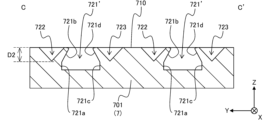
- FIG. 13 is a partial top view illustrating a first joint in which each recess has a second sub-recess formed therein; A cross-sectional view of the first joint portion shown in Figure 13 along line C-C'.
- FIG. 13 is a partial top view illustrating a first bonding portion in which a third sub-recess is formed in each recess.
- FIG. 13 is a partial top view illustrating a first bonding portion in which a fourth sub-recess is formed in each recess.
- FIG. 11 is a perspective view showing another example of a punch used to form a minor recess.
- FIG. 13 is a partial top view illustrating a first modified example of the arrangement of the roughening recesses.
- FIG. 13 is a partial top view illustrating a second modified example of the arrangement of the roughening recesses.
- FIG. 13 is a partial top view illustrating a third modified example of the arrangement of the roughening recesses.
- FIG. 13 is a partial top view illustrating a fourth modified example of the arrangement of the roughening recesses.
- FIG. 13 is a partial top view illustrating a fifth modified example of the arrangement of the roughening recesses.
- 1 is a schematic plan view showing an example of a vehicle to which a semiconductor device according to the present invention is applied;
- the X, Y, and Z axes in each of the referenced figures are shown for the purpose of defining the planes and directions in the illustrated semiconductor device, etc., and the X, Y, and Z axes are perpendicular to each other and form a right-handed system.
- the X direction may be referred to as the left-right direction
- the Y direction as the front-back direction
- the Z direction as the up-down direction.
- the plane including the X and Y axes may be referred to as the XY plane, the plane including the Y and Z axes as the YZ plane, and the plane including the Z and X axes as the ZX plane.
- These directions (front-back, left-right, up-down directions) and planes are terms used for convenience of explanation, and the corresponding relationship with each of the X, Y, and Z directions may change depending on the mounting posture of the semiconductor device.
- the heat dissipation surface side (cooler side) of the semiconductor device will be referred to as the bottom side, and the opposite side will be referred to as the top side.
- a planar view means a case where the top or bottom surface (XY plane) of the semiconductor device, etc. is viewed from the Z direction.
- the aspect ratios and size relationships between the various components in each figure are merely schematic representations and do not necessarily correspond to the relationships in the semiconductor device or other components that are actually manufactured. For the sake of convenience in explanation, it is assumed that the size relationships between the various components may be exaggerated.
- the semiconductor device exemplified in the following description is applied to a power conversion device such as an inverter for an industrial or automotive motor. For this reason, the following description will omit detailed descriptions of configurations, functions, operations, etc. that are the same as or similar to known semiconductor devices.
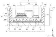
- FIG. 1 is a top view showing an example of the configuration of a semiconductor device according to one embodiment.
- FIG. 2 is a cross-sectional view of the semiconductor device in FIG. 1 taken along line A-A'.
- the sealing material filled in the case is omitted.
- the hatching showing the cross section of the sealing material filled in the case is omitted.
- the semiconductor device 1 is configured by placing a semiconductor module 2 on the upper surface of a cooler 3.
- the cooler 3 is an optional configuration for the semiconductor module 2.
- the cooler 3 dissipates heat from the semiconductor module 2 to the outside, and has an overall rectangular parallelepiped shape.
- the cooler 3 is configured by providing multiple fins on the underside of a flat base, and these fins are housed in a water jacket. Note that the shape and configuration of the cooler 3 are not limited to this and can be modified as appropriate.
- the semiconductor module 2 includes a base 4, a circuit board 5, a case 6, leads 7, bonding materials S1 to S4, bonding wires 8, and a sealing material 9.
- the base 4 is a substrate on which the circuit board 5 is mounted, and the base 4 on which the circuit board 5 is mounted is attached to the bottom surface of the case 6 with the surface on which the circuit board 5 is mounted facing upward.
- the case 6 includes a rectangular annular insulating member 601 with openings on the top and bottom surfaces, main terminals 602 and 603 integrated with the insulating member 601, and a plurality of control terminals 604.
- the circuit board 5 mounted on the base 4 is accommodated in the hollow portion of the insulating member 601 of the case 6.
- the base 4 is a metal plate such as a copper plate or an aluminum plate, and conducts heat generated by the circuit board 5 to the cooler 3. This type of base 4 may be called a heat sink or heat dissipation layer.
- the base 4, which is a heat sink, may be disposed on the top surface of the cooler 3 via a thermally conductive material such as thermal grease or thermal compound.
- the semiconductor module 2 may omit the base 4, and the bottom surface of the circuit board 5 (the conductor pattern 504 of the wiring board 500 illustrated in FIG. 2) may be joined to the cooler 3.
- the circuit board 5 includes a wiring board 500 and a semiconductor element 510 mounted on the upper surface of the wiring board 500.
- the wiring board 500 includes an insulating substrate 501, conductor patterns 502 and 503 provided on the upper surface of the insulating substrate 501, and a conductor pattern 504 provided on the lower surface of the insulating substrate 501.
- the wiring board 500 may be, for example, a DCB (Direct Copper Bonding) substrate or an AMB (Active Metal Brazing) substrate.
- the wiring board 500 may also be called a laminated substrate.
- the insulating substrate 501 is not limited to a specific substrate.
- the insulating substrate 501 may be, for example, a ceramic substrate formed of ceramic materials such as aluminum oxide (Al 2 O 3 ), aluminum nitride (AlN), silicon nitride (Si 3 N 4 ), aluminum oxide (Al 2 O 3 ) and zirconium oxide (ZrO 2 ).
- the insulating substrate 501 may be, for example, a substrate formed of insulating resin such as epoxy resin, a substrate formed by impregnating a base material such as glass fiber with insulating resin, or a substrate formed by coating the surface of a flat metal core with insulating resin.
- the conductor patterns 502 and 503 provided on the upper surface of the insulating substrate 501 are conductive members used as wiring members in the circuit board 5, and the conductor pattern 504 provided on the lower surface of the insulating substrate 501 is a conductive member used as a heat dissipation member that conducts heat generated in the circuit board 5 to the base 4. These conductor patterns 502 to 504 are formed, for example, from metal plates such as copper or aluminum.
- the conductor pattern 504 provided on the lower surface of the insulating substrate 501 is joined to the upper surface of the base 4 by a bonding material S1 such as solder.
- the conductor patterns 502 and 503 provided on the upper surface of the insulating substrate 501 may be called conductor layers, conductor plates, or wiring patterns.
- the conductor pattern 504 provided on the lower surface of the insulating substrate 501 may be called a heat dissipation layer, heat dissipation plate, or heat dissipation pattern.
- the conductor patterns 502 and 503 provided on the upper surface of the insulating substrate 501 are conductive members used as wiring members in the circuit board 5, as described above.
- a semiconductor element 510 is mounted on the upper surface of the first conductor pattern 502.
- the semiconductor element 510 has a first main electrode (not shown) provided on its lower surface joined to the first conductor pattern 502 by a bonding material S2.
- a second main electrode (not shown) and a control electrode 512 are provided on the upper surface of the semiconductor element 510. These electrodes are electrically insulated by an insulating layer (not shown) formed on the upper surface of the semiconductor element 510.
- the insulating layer may be a surface protective film such as a passivation film formed on the upper surface of the semiconductor element 510.
- the second main electrode is electrically connected to a second conductor pattern 503 provided on the upper surface of the insulating substrate 501 via a lead 7.
- the lead 7 includes a first joint 701, a second joint 702, and a wiring portion 703 connecting the first joint 701 and the second joint 702.
- the first joint 701 is electrically connected to the second main electrode of the semiconductor element 510 by a bonding material S3.
- the second joint 702 is bonded to the second conductor pattern 503 of the wiring board 500 by a bonding material S4.
- the control electrode 512 on the upper surface of the semiconductor element 510 is electrically connected to a control terminal 604 provided on the case 6 by a bonding wire 8.
- the first conductor pattern 502 is electrically connected to the first main terminal 602 provided on the case 6, and the second conductor pattern 503 is electrically connected to the second main terminal 603 provided on the case 6.
- the method of electrically connecting the first conductor pattern 502 and the first main terminal 602 and electrically connecting the second conductor pattern 503 and the second main terminal 603 may be any known connection method and is not limited to a specific method.
- the shape and position of the main terminals 602 and 603 in the case 6, the number and position of the control terminals 604, etc. are not limited to those illustrated and can be changed as appropriate.
- the case 6 of the semiconductor module 2 of this embodiment may be provided with a third main terminal, etc. (not illustrated).
- the semiconductor element 510 is, for example, composed of an RC (Reverse Conducting)-IGBT element that combines the functions of an IGBT (Insulated Gate Bipolar Transistor) element and an FWD (Free Wheeling Diode) element.
- RC Reverse Conducting
- IGBT Insulated Gate Bipolar Transistor
- FWD Free Wheeling Diode
- the semiconductor element mounted on the upper surface of the wiring board 500 is not limited to a specific one.
- the upper surface of the wiring board 500 may be mounted with a semiconductor element serving as a switching element such as an IGBT or a power MOSFET (Metal Oxide Semiconductor Field Effect Transistor), and a semiconductor element serving as a diode element such as an FWD.
- a reverse blocking (RB)-IGBT or the like having sufficient voltage resistance against reverse bias may be used as the semiconductor element.
- the semiconductor element is formed in a rectangular shape in a plan view using a semiconductor substrate such as silicon (Si) or silicon carbide (SiC). The shape, number, and location of the semiconductor element may be changed as appropriate.
- the layout of the conductor pattern as a wiring member provided on the upper surface side of the wiring board 500 is changed according to the type, shape, number, and location of the semiconductor element to be mounted.
- the switching element in the semiconductor element 510 is an IGBT element
- the second main electrode on the upper surface side may be called an emitter electrode
- the first main electrode on the lower surface side may be called a collector electrode.
- the switching element in the semiconductor element 510 is a MOSFET element
- the second main electrode on the upper surface side may be called a source electrode
- the first main electrode on the lower surface side may be called a drain electrode.
- the control electrode 512 provided on the upper surface of the semiconductor element 510 may include a gate electrode and an auxiliary electrode.
- the auxiliary electrode may be an auxiliary emitter electrode or an auxiliary source electrode that is electrically connected to the second main electrode and serves as a reference potential for the gate potential.
- the auxiliary electrode may be a temperature sense electrode that is electrically connected to the temperature sense unit and measures the temperature of the semiconductor element 510.
- Such electrodes formed on the upper surface of the semiconductor element 510 may be collectively called upper surface electrodes.
- the above-mentioned lead 7 is formed by bending a metal plate such as a copper plate, and may be called a lead frame or a metal wiring plate.
- An insulating layer is formed on the upper surface of the semiconductor element 510 so as to surround a second main electrode that is electrically connected to the first joint portion 701 of the lead 7.
- the insulating layer surrounding the second main electrode restricts the spreading of the bonding material S3 that bonds the second main electrode to the first joint portion 701 of the lead 7 within a plane (XY plane) when melted.
- the end of the wiring portion 703 of the lead 7 on the side of the first joint 701 is connected to one side of the first joint 701, and is bent from that side in the opposite direction to the bottom surface of the first joint 701 (in other words, the surface of the first joint 701 that faces the second main electrode of the semiconductor element 510).
- the end of the wiring portion 703 of the lead 7 on the side of the second joint 702 is connected to one side of the second joint 702, and is bent from that side in the opposite direction to the bottom surface of the second joint 702 (in other words, the surface of the second joint 702 that faces the conductor pattern 503).
- the sealing material 9 may be a single insulating material, or a combination of multiple types of insulating materials with different compositions (characteristics).
- the sealing material 9 may include a coating agent such as PA (polyamide) that is coated on the surfaces of the semiconductor element 510 and the leads 7, etc., and an insulating material such as epoxy resin that is additionally filled in after coating with the coating agent.
- the upper surface (the surface opposite to the surface facing the semiconductor element 510) of the first bonding portion 701 of the lead 7 is subjected to a roughening treatment to prevent peeling at the interface between the first bonding portion 701 and the sealing material 9.
- a plurality of recesses (hereinafter referred to as “roughening recesses") are provided on the upper surface of the first bonding portion 701.
- a first example of a plurality of roughening recesses provided on the upper surface of the first bonding portion 701 will be described below with reference to FIGS. 3 to 5.
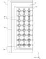
- FIG. 3 is a partial top view of an enlarged region R in FIG. 1.
- FIG. 4 is a partial top view of an enlarged roughening recess (720) formed in the portion shown in FIG. 3.
- FIG. 5 is a cross-sectional view taken along line B-B' in FIG. 4.
- FIG. 6 is a diagram for explaining an example of the formation position and dimensions of the recess that becomes the main recess and the sub-recess.
- the sealing material 9 that fills the case 6 and overlaps above the first bonding portion 701 of the lead 7 is omitted.
- the cross-sectional view in FIG. 5 shows only a portion of the upper surface side of the first bonding portion 701 and a portion of the sealing material 9, and the hatching showing the cross section of the sealing material 9 filled in the case 6 is omitted.
- one roughening recess 720 is composed of a main recess 721 and four sub-recesses 722-725, as illustrated in Figures 3 and 4.
- the main recess 721 is formed by deforming a recess 721' that defines a space in the shape of a rectangular prism with a flat bottom formed on the upper surface 710 of the first joint 701 using the four sub-recesses 722-725, as described later with reference to Figures 6 and 7-9.
- Each of the four sub-recesses 722-725 has a square opening end and is a recess that defines a space in the shape of a quadrangular pyramid with the opening end as the bottom, and is formed so that one surface of the quadrangular pyramid deforms one wall surface of the recess 721' before it is made into the main recess 721 toward the opposing wall surface.
- One sub-recess e.g., the sub-recess 722 located to the left of the main recess 721 in Figs.
- the dimensions of the bottom surface and depth of the main recess 721 and the sub recesses 722-725 are not limited to a specific combination of values. If the shape of the opening end of the recess 721' before it is made into the main recess 721 in a plan view and the opening ends of the sub recesses 722-725 are each approximately square, the length L2 of the side of the sub recesses 722-725 may be shorter than the length L1 of the side of the recess 721'.
- the distance L3 between the center (position of the apex angle) of the sub recesses 722-725 in a plan view and the side of the recess 721' may be L3 ⁇ L2/2.
- the gap L4 between two adjacent recesses 721' before it is made into the main recess 721 is set to be longer than the length L1 of the side of the recess 721' to such an extent that the sub recess that deforms the wall surface of one recess 721' and the sub recess that deforms the wall surface of the other recess 721' do not communicate with each other to form a single recess.
- the gap L4 is set to, for example, 0.18 mm. Note that the combination of the side lengths L1, L2, distance L3, and gap L4 described above is not limited to a specific combination and can be changed as appropriate.
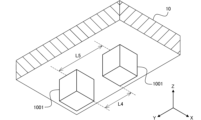
- FIG. 7 is a perspective view illustrating a punch used to form the recess that becomes the main recess.
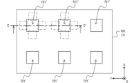
- FIG. 8 is a partial top view illustrating a recess formed in the first joint of the lead by the punch illustrated in FIG. 7.
- FIG. 9 is a cross-sectional view along the line C-C' in the first joint shown in FIG. 8.
- FIG. 10 is a perspective view illustrating a punch used to form the sub-recess.
- FIG. 11 is a partial top view illustrating a sub-recess formed in the first joint of the lead by the punch illustrated in FIG. 10.
- FIG. 12 is a cross-sectional view along the line C-C' in the first joint shown in FIG. 11.
- FIG. 13 is a partial top view illustrating a first joint in which a second sub-recess is formed in each recess.
- FIG. 14 is a cross-sectional view along the line C-C' in the first joint shown in FIG. 13.
- FIG. 15 is a partial top view illustrating a first joint in which a third sub-recess is formed in each recess.
- FIG. 16 is a partial top view illustrating a first joint in which a fourth sub-recess is formed in each recess.
- the process of forming the roughening recess 720 consisting of one main recess 721 and four sub-recesses 722 to 725 described above with reference to Figures 3 to 6 includes, for example, a process of forming a recess 721' that becomes the main recess 721, followed by a process of forming the four sub-recesses 722 to 725.
- a die 10 is used in which a plurality of rectangular prism-shaped punches (pressing dies) 1001 are arranged adjacent to each other with a gap L4 in each of the X and Y directions to form a plurality of recesses 721' in a two-dimensional lattice pattern.
- a recess 721' that defines a rectangular prism-shaped space of depth D1 is formed on the upper surface 710 of the first joint 701 of the lead 7.
- the depth D1 of the recess 721' is set to be sufficiently small compared to the thickness of the first joint 701 (not shown), for example, about 0.05 mm.
- the plurality of recesses 721' may be formed on the entire upper surface 710 of the first joint 701 at once, or may be formed in a plurality of steps.
- the four sub-recesses 722-725 for one recess 721' are formed one at a time in four separate steps.
- a die 11 having a plurality of punches 1101 is used, in which one punch 1101 is arranged for a region R2 corresponding to a punch 1001 that forms one recess 721'.
- the punches 1101 are, for example, pyramidal with a convex tip, and are arranged in such a direction that each side of the pyramid at the tip is parallel to one of the four sides at the opening end of the recess 721' when the die 11 is placed above the first joint 701 of the lead 7.
- the punches 1101 are arranged at the same interval L5 as the interval L5 of the punch 1001 that forms the recess 721'. As described above with reference to FIG. 7, the interval L5 is the distance between the centers of two punches 1001 adjacent to each other at the gap L4.
- the sub-recess 723 is formed to the right of the recess 721' in plan view (negative side in the Y direction) as the first sub-recess for each recess 721' using the punch 1101 of the mold 11.
- the sub-recess 723 is formed by aligning the first joint 701 of the lead 7 with the mold 11 so that the apex of the pyramid at the tip of the punch 1101 is outside the opening end of the recess 721' and is at a distance L3 from the right side of the opening end (see FIG. 6) in plan view.
- one of the triangular slopes of the pyramid at the tip of the punch 1101 displaces the metal material portion between the slope and the wall surface 721c of the recess 721' in the direction of the wall surface 721a facing the wall surface 721c.
- a return portion 721d protruding in the direction of the wall surface 721a is formed on the wall surface 721c.
- the relationship between the depth D2 of the sub-recess 723 and the depth D1 of the recess 721' is not limited to the relationship D2 ⁇ D1 illustrated in FIG. 12.
- the position of the sub-recess 723 relative to the recess 721', the ratio of the dimensions of the opening ends, the ratio of the depths, the angle of the apex of the pyramid at the tip of the punch 1101, etc. can be changed as appropriate according to, for example, the desired protrusion amount L6 of the return portion 721d from the wall surface 721c.
- a return portion 721d may be formed in which the entire wall surface 721c protrudes toward the opposing wall surface 721a.
- FIG. 13 and 14 show an example in which the punch 1101 of the die 11 is used to form a sub-recess 722 to the left of the recess 721' in plan view (positive Y direction) as a second sub-recess for each recess 721'.
- the first joint 701 of the lead 7 and the die 11 are aligned so that the apex of the pyramid at the tip of the punch 1101 is outside the opening end of the recess 721' and is at a distance L3 from the left side of the opening end (see FIG. 6) in plan view, and the sub-recess 722 is formed.
- the sub-recess 722 is formed to a depth D2 under the same processing conditions (pressure conditions) as when the sub-recess 723 was formed.
- one of the triangular slopes of the pyramid at the tip of the punch 1101 displaces the metal material portion between the slope and the wall surface 721a of the recess 721' in the direction of the wall surface 721c on which the return portion 721d facing the wall surface 721a is formed. This forms a return portion 721b on wall surface 721a that protrudes toward wall surface 721c.
- FIG. 15 shows an example in which a sub-recess 724 is formed above the recess 721' (positive side in the X direction) in a plan view as a third sub-recess for each recess 721' using the punch 1101 of the mold 11.
- the first joint 701 of the lead 7 and the mold 11 are aligned so that the apex of the pyramid at the tip of the punch 1101 is outside the opening end of the recess 721' and is at a distance L3 from the upper side of the opening end (see FIG. 6) in a plan view, and the sub-recess 724 is formed.
- the sub-recess 724 is formed to a depth D2 under the same processing conditions (pressure conditions) as when the sub-recesses 722 and 723 were formed.
- one of the triangular slopes of the pyramid at the tip of the punch 1101 displaces the metal material portion between the slope and the wall surface 721e of the recess 721' in the direction of the wall surface 721g facing the wall surface 721e. This forms a return portion 721f on wall surface 721e that protrudes toward wall surface 721g.
- FIG. 16 shows an example in which a punch 1101 of the die 11 is used to form a sub-recess 725 below the recess 721' in plan view (negative side in the X direction) as a fourth sub-recess for each recess 721'.
- the first joint 701 of the lead 7 and the die 11 are aligned so that the apex of the pyramid at the tip of the punch 1101 is outside the opening end of the recess 721' and is at a distance L3 from the lower side of the opening end in plan view (see FIG. 6), forming the sub-recess 725.
- the sub-recess 725 is formed to a depth D2 under the same processing conditions (pressure conditions) as those used to form the sub-recesses 722 to 724.
- one of the triangular slopes of the pyramid at the tip of the punch 1101 displaces the metal material portion between the slope and the wall surface 721g of the recess 721' in the direction of the wall surface 721e on which the return portion 721f facing the wall surface 721g is formed. This forms a return portion 721h on wall surface 721g that protrudes toward wall surface 721e.
- the sub-concave portions 722 to 725 are formed under processing conditions that result in a depth of D2, but the depth of all the sub-concave portions may not be the same.
- the stress (thermal strain) occurring at the interface between the upper surface 710 of the first bonding portion 701 and the sealing material 9 differs between the X direction and the Y direction
- peeling of the sealing material 9 at either the end in the X direction or the end in the Y direction may occur more easily than peeling of the sealing material 9 at the other end.
- peeling of the sealing material 9 may occur more easily on the outer periphery side of the upper surface 710 of the roughening recess 720 than on the inner side.
- the sub-concave portion along the side of the roughening recess 720 located along the edge located at the end in the direction in which the greater stress (thermal strain) occurs may be made slightly deeper than D2 to increase the size of the folded portion formed on the wall surface.
- a plurality of roughening recesses 720 are formed on the upper surface 710 of the first joint portion 701 in the lead 7 according to this embodiment, including a main recess 721 having return portions 721b, 721d, 721f, and 721h on the wall surface.
- the insulating material as the sealing material 9 is filled into the main recess 721 of the roughening recess 720, the movement of the filled portion in the direction of coming out of the main recess 721 (positive side of the Z direction) is restricted by the return portions 721b, 721d, 721f, and 721h, making it difficult for the filled portion to come out of the main recess 721.
- the roughening recess 720 has four sub-recesses 722 to 725, each of which defines a quadrangular pyramid-shaped space, formed at positions that are outside the main recess 721 in a plan view.
- the area of the interface between the upper surface 710 of the first bonding portion 701 of the lead 7 and the sealing material 9 in the region where one roughening recess 720 is formed is increased, and the adhesion between the first bonding portion 701 and the sealing material 9 is improved.
- the semiconductor device 1 semiconductor module 2 of this embodiment can make it difficult for the interface between the first bonding portion 701 of the lead 7 and the sealing material 9 to peel off, and can suppress the occurrence of failures due to peeling, compared to the case where only the recess 721' that defines the quadrangular prism-shaped space illustrated in FIGS. 8 and 9 is formed on the upper surface 710 of the first bonding portion 701 by the punch 1001 illustrated in FIG. 7, for example.
- the roughening recess 720 can further improve the adhesion between the upper surface 710 of the first bonding portion 701 and a coating agent such as PA that is coated on the surface of the lead 7, etc., in order to prevent an increase in distortion that occurs in the defective portion due to the sealing resin such as epoxy resin as the sealing material 9 peeling off from the first bonding portion 701.
- the process of forming multiple sub-recesses for one recess 721' can be performed multiple times. Therefore, the constraints on the processing dimensions when forming the sub-recesses are relatively relaxed, and it is easy to form return portions with the desired amount of protrusion.
- the punch 1101 with a pyramidal tip described above with reference to FIG. 10 is merely an example of a punch that can be used to form the secondary recesses 722-725 for forming the main recess 721 having return portions 721b, 721d, 721f, and 721h on the wall surface.
- the tip of the punch (pressing die) used to form the secondary recesses 722-725 may have a different shape.
- FIG. 17 is a perspective view showing another example of a punch used to form a secondary recess.
- mountain-shaped (wedge-shaped) punches 1201 each having a tip portion formed of two flat surfaces, are arranged in a two-dimensional lattice pattern.
- the punch 1201 shown in FIG. 17 is arranged in a region R2 corresponding to the punch 1001 that forms one recess 721', similar to the punch 1101 of the mold 11 shown in FIG. 11.
- the punches 1201 are arranged at intervals L5, which are the same as the intervals L5 of the punches 1001 that form the recess 721'.
- the interval L5 is the distance between the centers of two punches 1001 adjacent to each other across the gap L4.
- the multiple punches 1201 are arranged in a two-dimensional lattice pattern so that the extension directions of the ridges of the tips are in the same direction (the X direction in FIG. 17).
- the first joint 701 of the lead 7 is aligned with the die 12 so that the ridgeline of the tip of the punch 1201 is outside the open end of the recess 721' and parallel to the side corresponding to the side on which the return portion is formed by the punch 1201 at a distance L3 from the side, forming the sub-recess.
- the sub-recess formed by each punch 1201 becomes a valley-shaped space having a valley line extending in a direction parallel to the ridgeline of the tip of the punch 1201.
- the plane located between the ridgeline and the wall of the recess 721' one of the two planes that form the mountain shape of the tip of the punch 1201, displaces the metal material portion between that plane and the wall of the recess 721', forming the return portion.
- a first die in which the extension direction of the ridge line of punch 1201 is a first direction in order to form a return portion on a side surface of recess 721' that is parallel to a first direction (X direction), and a second die in which the extension direction of the ridge line of punch 1201 is a second direction in order to form a return portion on a side surface of recess 721' that is parallel to a second direction (Y direction) may be prepared.
- X direction first direction
- a second die in which the extension direction of the ridge line of punch 1201 is a second direction in order to form a return portion on a side surface of recess 721' that is parallel to a second direction (Y direction)
- a common die 12 may be used for the process of forming return portions on the side surfaces of the recess 721' parallel to the first direction (X direction) and the process of forming return portions on the side surfaces of the recess 721' parallel to the second direction (Y direction), and the die 12 may be rotated for each process so that the extension direction of the ridge of the punch 1201 is parallel to the side surfaces on which the return portions are formed.
- each of the four sub-recesses for one recess 721' may be formed using a different mold.
- the tip of the punch in one mold used to form one sub-recess may have a shape that allows a return portion to be formed on a desired wall surface of the recess 721'.
- a sub-recess may be formed using a mold in which single-edged punches are arranged two-dimensionally.
- the arrangement of the multiple roughening recesses 720 described in the above embodiment is not limited to the arrangement in a two-dimensional lattice pattern on the entire upper surface 710 of the first joint 701 of the lead 7 as illustrated in FIG. 3.
- the multiple roughening recesses 720 may be arranged only in a predetermined area on the upper surface 710.
- the roughening recesses 720 including the main recess 721 and the sub-recesses 722 to 725, and a recess that does not include a sub-recess and does not have a return portion formed on the wall surface (for example, the recess 721' that defines the above-mentioned rectangular column-shaped space) may be arranged on the upper surface 710 of the first joint 701. That is, in the above embodiment, the recess 721' that defines a rectangular space may be formed on the upper surface 710 of the first joint 701 as a second roughening recess separate from the roughening recess 720.
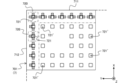
- FIG. 18 is a partial top view illustrating a first modified example of the arrangement of the roughening recesses.
- FIG. 19 is a partial top view illustrating a second modified example of the arrangement of the roughening recesses.
- FIG. 20 is a partial top view illustrating a third modified example of the arrangement of the roughening recesses.
- FIG. 21 is a partial top view illustrating a fourth modified example of the arrangement of the roughening recesses.
- FIG. 22 is a partial top view illustrating a fifth modified example of the arrangement of the roughening recesses.
- the upper surface 710 of the first joint 701 of the lead 7 is generally a flat surface, and as illustrated in FIG. 3, the roughening recesses 720 can be formed in a two-dimensional lattice pattern on the entire upper surface 710.
- a region having a function different from the roughening recesses may be partially provided on the upper surface 710 of the first joint 701.
- the roughening recesses 720 may not be formed in the region in which the roughening recesses 720 cannot be formed.
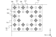
- 19 and 20 show an example in which roughening recesses 720 including a main recess 721 and sub recesses 722-725, and recesses 721' in which a return portion using a sub recess is not formed are arranged in a two-dimensional lattice on the upper surface 710 of the first bonding portion 701 of the lead 7. It is known that peeling at the interface between the upper surface 710 of the first bonding portion 701 and the sealing material 9 occurs at the outer periphery of the upper surface 710 of the first bonding portion 701 and progresses in a direction perpendicular to the side of the upper surface 710. For this reason, as illustrated in FIGS.
- recesses 721' without return portions formed by the punch 1001 illustrated in FIG. 7 may be arranged as second roughening recesses.
- FIG. 19 shows an example in which, of the two-dimensional lattice set on the upper surface 710 of the first bonding portion 701 in a plan view, a row along the side 711 closest to the side 711 and a column along the side 712 closest to the side 712 are roughening recesses 720.
- the recesses for preventing peeling of the sealant 9 arranged in a two-dimensional lattice on the upper surface 710 of the first bonding portion 701 only the recesses arranged in a ring shape on the outermost periphery are roughening recesses 720 including the main recesses 721 and the secondary recesses 722 to 725, and recesses 721' that do not have a return portion are arranged within the area surrounded by the ring-shaped roughening recesses 720.
- the recesses 721' that do not have a return portion are not arranged in an area of the upper surface 710 of the first bonding portion 701 where a recess for preventing peeling of the sealant 9 cannot be formed.
- FIG. 20 also shows an example in which two rows along side 711 and two columns along side 712 of a two-dimensional lattice set on the upper surface 710 of the first bonding portion 701 in a plan view are roughening recesses 720.
- the recesses for preventing peeling of the sealant 9 arranged in a two-dimensional lattice on the upper surface 710 of the first bonding portion 701 only the recesses arranged in a ring shape on the outermost circumference and the second outer circumference adjacent to the outermost circumference are roughening recesses 720 including the main recesses 721 and the sub recesses 722 to 725, and recesses 721' that do not have a return portion are arranged in the area surrounded by the annularly arranged roughening recesses 720.
- the recesses 721' that do not have a return portion are not arranged in an area of the upper surface 710 of the first bonding portion 701 where a recess for preventing peeling of
- the number of rows and columns in which the roughening recesses 720 including the main recess 721 and the sub recesses 722 to 725 having a return portion are arranged on the upper surface 710 of the first joint 701 in a plan view is not limited to a specific combination.
- the number of rows and columns in which the roughening recesses 720 are arranged may be set, for example, according to the dimension of the upper surface 710 of the first joint 701 in a first direction (X direction) and the dimension of the second direction (Y direction) perpendicular to the first direction.
- the stress (thermal strain) generated at the interface between the upper surface 710 of the first joint 701 and the sealing material 9 differs between the X direction and the Y direction, peeling of the sealing material 9 at either the end in the X direction or the end in the Y direction may occur more easily than peeling of the sealing material 9 at the other end.
- the number of rows or columns of the roughening recesses 720 along the side located at the end in the direction in which the greater stress (thermal strain) occurs may be greater than the number of columns or rows of the roughening recesses 720 along the side located at the end in the direction in which the smaller stress (thermal strain) occurs.
- FIG. 21 shows yet another example in which roughening recesses 720 including a main recess 721 and sub recesses 722-725 and recesses 721' without a return portion using a sub recess are arranged in a two-dimensional lattice on the upper surface 710 of the first joint 701 of the lead 7.
- the roughening recesses 720 with a return portion and the recesses 721' without a return portion are arranged so as to be adjacent to each other in the directions (X direction and Y direction) of the unit translation vector representing the two-dimensional lattice in which the roughening recesses 720 and the recesses 721' are arranged.
- the roughening recesses 720 with a return portion and the recesses 721' without a return portion are arranged alternately in the first direction (X direction) and the second direction (Y direction) on the upper surface 710 of the first joint 701.
- the arrangement of the roughening recesses 720 and the arrangement of the recesses 721' illustrated in FIG. 21 may each be called a staggered arrangement.
- FIG. 22 shows a modified example of a roughening recess 720 including a main recess 721 with a return portion formed on the wall surface by a sub-recess.
- return portions 721b, 721d, 721f, and 721h are formed on each of the four wall surfaces 721a, 721c, 721e, and 721g of a recess 721' that defines a rectangular prism-shaped space, protruding toward the opposing wall surface by the sub-recess.
- each of the roughening recesses 720 illustrated in FIG. 22 has a sub-recess formed at least between the main recess 721 and one of the sides of the upper surface 710 of the first bonding portion 701 that is closest to the main recess 721. Note that the positions and number of the sub-recesses relative to the main recess 721 in the roughening recess 720 are not limited to those illustrated in FIG. 22.
- the roughening recess 720 described above with reference to the drawings is merely an example of a roughening recess including a main recess in which a return portion is formed that protrudes toward one or more wall surfaces of the recess, and a sub-recess that is outside the main recess in a plan view, has a center at a position a predetermined distance L3 away from the wall surface on which the return portion is formed, and has an inclined surface that becomes shallower from the center toward the opening end of the main recess.
- the relationship between the main recess and one or more sub-recesses in the roughening recess 720 is not limited to the example described above with reference to the drawings, and various changes and modifications are possible.
- the recess that does not form a return portion by the sub-recess is not limited to the recess 721' that defines a quadrangular prism-shaped space used to form the main recess 721, but may also be a recess that defines a space of another shape.
- the semiconductor device 1 including the semiconductor module 2 of this embodiment can be applied to a power conversion device such as an inverter for an in-vehicle motor.
- a power conversion device such as an inverter for an in-vehicle motor.
- FIG. 23 is a schematic plan view showing an example of a vehicle to which the semiconductor device according to the present invention is applied.
- the vehicle 2001 shown in FIG. 23 is, for example, a four-wheeled vehicle equipped with four wheels 2002.
- the vehicle 2001 may be, for example, an electric vehicle in which the wheels are driven by a motor or the like, or a hybrid vehicle that uses power from an internal combustion engine in addition to a motor.
- the vehicle 2001 includes a drive unit 2003 that applies power to the wheels 2002, and a control device 2004 that controls the drive unit 2003.
- the drive unit 2003 may be composed of at least one of an engine, a motor, or a hybrid of an engine and a motor, for example.
- the control device 2004 controls (e.g., power control) the drive unit 2003 described above.
- the control device 2004 includes the semiconductor device 1 described above.
- the semiconductor device 1 may be configured to perform power control for the drive unit 2003.
- the semiconductor module 2 of the semiconductor device 1 used in this type of vehicle 2001 if the first joint 701 of the lead 7 described above is joined to the electrode on the top surface of the semiconductor element (e.g., the second main electrode of the semiconductor element 510) with the joining material S3, it is possible to prevent the progression of peeling at the interface between the sealing material 9 and the top surface 710 of the first joint 701. This makes it possible to reduce the frequency of inspection and replacement of the semiconductor device 1 used in the vehicle 2001.
- the semiconductor element e.g., the second main electrode of the semiconductor element 510
- vehicle to which the semiconductor device 1 is applied is not limited to a four-wheeled vehicle as illustrated in FIG. 23.
- Vehicles to which the semiconductor device 1 is applied include, for example, two-wheeled vehicles and railroad cars.
- the present embodiment is not limited to the above-mentioned embodiment and modifications, and may be modified, substituted, or altered in various ways without departing from the spirit of the technical idea. Furthermore, if the technical idea can be realized in a different way due to technological advances or derived other technologies, it may be implemented using that method. Therefore, the scope of the claims covers all embodiments that may fall within the scope of the technical idea.
- the semiconductor module according to the above embodiment includes a circuit board on which a semiconductor element is mounted, a lead bonded to an electrode on the upper surface of the semiconductor element by a bonding material, and a sealing material that seals the semiconductor element and the lead.
- the lead has a roughening recess formed on the upper surface opposite the lower surface facing the electrode at the bonding portion bonded to the electrode to prevent peeling at the interface between the lead and the sealing material.
- the roughening recess includes a main recess having a return portion that protrudes toward one or more wall surfaces of the recess, and a sub-recess that is outside the main recess in a plan view, has a center at a position a predetermined distance away from the wall surface on which the return portion is formed, and has a slope that becomes shallower from the center toward the opening end of the main recess.
- the main recess is a rectangle with a flat bottom surface
- the sub-recess has a square opening end and is shaped to define a quadrangular pyramidal space with the opening end as the bottom surface, and each side of the opening end of the sub-recess is approximately parallel to one of the sides of the bottom surface of the main recess.
- the main recess has a rectangular shape with a flat bottom
- the sub-recess has a rectangular opening end and a shape that defines a valley-shaped space with a valley line that is approximately parallel to the sides of the opening end and the sides of the bottom surface of the main recess.
- the main recess has a shape in which the return portion is formed on each of the four wall surfaces of the recess that defines a rectangular prism-shaped space.
- the gap between the main recesses of two adjacent roughening recesses is longer than the dimension of the main recess in the direction in which the two roughening recesses are adjacent.
- the roughening recesses are arranged at positions corresponding to the lattice points of a two-dimensional lattice set on the upper surface of the first joint portion of the lead.
- the roughening recess in which the return portion is formed and the second roughening recess without the return portion are arranged adjacent to each other at positions corresponding to the lattice points of the two-dimensional lattice.
- the roughening recess is arranged in a ring shape along the edge of the top surface of the first joint.
- a second roughening recess that does not have a return portion is disposed within an area surrounded by the annularly arranged roughening recesses on the upper surface of the first joint.
- the semiconductor device includes the above semiconductor module and a cooler arranged on the surface of the circuit board of the semiconductor module opposite to the surface on which the semiconductor element is mounted.
- the vehicle according to the above embodiment is equipped with the above semiconductor module or semiconductor device.
- the present invention has the effect of preventing peeling at the interface between the upper surface of the joint of the lead that is joined to the electrode of the semiconductor element and the sealing material, and is particularly useful for industrial or electrical semiconductor modules, semiconductor devices, and vehicles.
Landscapes
- Structures Or Materials For Encapsulating Or Coating Semiconductor Devices Or Solid State Devices (AREA)
Priority Applications (3)
| Application Number | Priority Date | Filing Date | Title |
|---|---|---|---|
| JP2024552856A JP7827161B2 (ja) | 2022-10-25 | 2023-08-31 | 半導体モジュール、半導体装置、及び車両 |
| CN202380031428.XA CN118974917A (zh) | 2022-10-25 | 2023-08-31 | 半导体模块、半导体装置以及车辆 |
| US18/902,281 US20250022833A1 (en) | 2022-10-25 | 2024-09-30 | Semiconductor module, semiconductor device, and vehicle |
Applications Claiming Priority (2)
| Application Number | Priority Date | Filing Date | Title |
|---|---|---|---|
| JP2022-170593 | 2022-10-25 | ||
| JP2022170593 | 2022-10-25 |
Related Child Applications (1)
| Application Number | Title | Priority Date | Filing Date |
|---|---|---|---|
| US18/902,281 Continuation US20250022833A1 (en) | 2022-10-25 | 2024-09-30 | Semiconductor module, semiconductor device, and vehicle |
Publications (1)
| Publication Number | Publication Date |
|---|---|
| WO2024090029A1 true WO2024090029A1 (ja) | 2024-05-02 |
Family
ID=90830593
Family Applications (1)
| Application Number | Title | Priority Date | Filing Date |
|---|---|---|---|
| PCT/JP2023/031781 Ceased WO2024090029A1 (ja) | 2022-10-25 | 2023-08-31 | 半導体モジュール、半導体装置、及び車両 |
Country Status (4)
| Country | Link |
|---|---|
| US (1) | US20250022833A1 (https=) |
| JP (1) | JP7827161B2 (https=) |
| CN (1) | CN118974917A (https=) |
| WO (1) | WO2024090029A1 (https=) |
Citations (6)
| Publication number | Priority date | Publication date | Assignee | Title |
|---|---|---|---|---|
| JP2006510221A (ja) * | 2002-12-13 | 2006-03-23 | フリースケール セミコンダクター インコーポレイテッド | オーバーモールド・プラスチック・パッケージ用ヒートシンクまたはフラグ用の微小モールドロック |
| JP2007305916A (ja) * | 2006-05-15 | 2007-11-22 | Rohm Co Ltd | リードフレームの製造方法および製造装置 |
| JP2008211168A (ja) * | 2007-01-31 | 2008-09-11 | Mitsubishi Electric Corp | 半導体装置および半導体モジュール |
| JP2013157536A (ja) * | 2012-01-31 | 2013-08-15 | Shinko Electric Ind Co Ltd | リードフレーム及びその製造方法と半導体装置及びその製造方法 |
| JP2017208486A (ja) * | 2016-05-19 | 2017-11-24 | 株式会社ミスズ工業 | 表面に凹凸を有する金属部材、ヒートスプレッダ、半導体パッケージ及びそれらの製造方法 |
| WO2022004758A1 (ja) * | 2020-06-30 | 2022-01-06 | 富士電機株式会社 | 半導体モジュールおよび半導体モジュールの製造方法 |
-
2023
- 2023-08-31 CN CN202380031428.XA patent/CN118974917A/zh active Pending
- 2023-08-31 JP JP2024552856A patent/JP7827161B2/ja active Active
- 2023-08-31 WO PCT/JP2023/031781 patent/WO2024090029A1/ja not_active Ceased
-
2024
- 2024-09-30 US US18/902,281 patent/US20250022833A1/en active Pending
Patent Citations (6)
| Publication number | Priority date | Publication date | Assignee | Title |
|---|---|---|---|---|
| JP2006510221A (ja) * | 2002-12-13 | 2006-03-23 | フリースケール セミコンダクター インコーポレイテッド | オーバーモールド・プラスチック・パッケージ用ヒートシンクまたはフラグ用の微小モールドロック |
| JP2007305916A (ja) * | 2006-05-15 | 2007-11-22 | Rohm Co Ltd | リードフレームの製造方法および製造装置 |
| JP2008211168A (ja) * | 2007-01-31 | 2008-09-11 | Mitsubishi Electric Corp | 半導体装置および半導体モジュール |
| JP2013157536A (ja) * | 2012-01-31 | 2013-08-15 | Shinko Electric Ind Co Ltd | リードフレーム及びその製造方法と半導体装置及びその製造方法 |
| JP2017208486A (ja) * | 2016-05-19 | 2017-11-24 | 株式会社ミスズ工業 | 表面に凹凸を有する金属部材、ヒートスプレッダ、半導体パッケージ及びそれらの製造方法 |
| WO2022004758A1 (ja) * | 2020-06-30 | 2022-01-06 | 富士電機株式会社 | 半導体モジュールおよび半導体モジュールの製造方法 |
Also Published As
| Publication number | Publication date |
|---|---|
| JPWO2024090029A1 (https=) | 2024-05-02 |
| US20250022833A1 (en) | 2025-01-16 |
| CN118974917A (zh) | 2024-11-15 |
| JP7827161B2 (ja) | 2026-03-10 |
Similar Documents
| Publication | Publication Date | Title |
|---|---|---|
| US10825758B2 (en) | Semiconductor device | |
| JP7735655B2 (ja) | 半導体装置 | |
| JP7568132B2 (ja) | 半導体モジュール及び半導体装置 | |
| CN112236855B (zh) | 半导体装置 | |
| CN111341731A (zh) | 半导体装置 | |
| JP2005243685A (ja) | 半導体装置 | |
| JP7827161B2 (ja) | 半導体モジュール、半導体装置、及び車両 | |
| US20240021569A1 (en) | Semiconductor module and method for manufacturing semiconductor module | |
| US20240145353A1 (en) | Semiconductor module, method for manufacturing semiconductor module, semiconductor device, and vehicle | |
| US12412847B2 (en) | Semiconductor module, semiconductor device and vehicle | |
| WO2025017957A1 (ja) | 半導体装置 | |
| JP7798206B2 (ja) | 半導体モジュール、半導体装置、及び車両 | |
| JP7543854B2 (ja) | 半導体装置及び半導体装置の製造方法 | |
| US20240112991A1 (en) | Semiconductor module, semiconductor device, and vehicle | |
| US20240136319A1 (en) | Semiconductor module, semiconductor device, and vehicle | |
| US20250062271A1 (en) | Semiconductor module and method for manufacturing semiconductor module | |
| JP7634456B2 (ja) | 半導体装置 | |
| JP2024072092A (ja) | 半導体モジュール及び半導体装置 | |
| WO2024095710A1 (ja) | 半導体モジュール | |
| JP2023118481A (ja) | 半導体装置及び車両 | |
| WO2025164363A1 (ja) | モジュール | |
| WO2024095712A1 (ja) | 半導体モジュール | |
| WO2024095714A1 (ja) | 半導体モジュール | |
| JP2025176521A (ja) | 半導体装置 | |
| WO2024128062A1 (ja) | 半導体装置 |
Legal Events
| Date | Code | Title | Description |
|---|---|---|---|
| 121 | Ep: the epo has been informed by wipo that ep was designated in this application |
Ref document number: 23882243 Country of ref document: EP Kind code of ref document: A1 |
|
| ENP | Entry into the national phase |
Ref document number: 2024552856 Country of ref document: JP Kind code of ref document: A |
|
| WWE | Wipo information: entry into national phase |
Ref document number: 202380031428.X Country of ref document: CN |
|
| NENP | Non-entry into the national phase |
Ref country code: DE |
|
| 122 | Ep: pct application non-entry in european phase |
Ref document number: 23882243 Country of ref document: EP Kind code of ref document: A1 |