WO2024075810A1 - 有機光電変換膜、有機光電変換素子、有機光電変換膜の製造方法、及び有機半導体インク組成物 - Google Patents
有機光電変換膜、有機光電変換素子、有機光電変換膜の製造方法、及び有機半導体インク組成物 Download PDFInfo
- Publication number
- WO2024075810A1 WO2024075810A1 PCT/JP2023/036345 JP2023036345W WO2024075810A1 WO 2024075810 A1 WO2024075810 A1 WO 2024075810A1 JP 2023036345 W JP2023036345 W JP 2023036345W WO 2024075810 A1 WO2024075810 A1 WO 2024075810A1
- Authority
- WO
- WIPO (PCT)
- Prior art keywords
- photoelectric conversion
- organic semiconductor
- type organic
- organic photoelectric
- ink composition
- Prior art date
- Legal status (The legal status is an assumption and is not a legal conclusion. Google has not performed a legal analysis and makes no representation as to the accuracy of the status listed.)
- Ceased
Links
Images
Classifications
-
- H—ELECTRICITY
- H10—SEMICONDUCTOR DEVICES; ELECTRIC SOLID-STATE DEVICES NOT OTHERWISE PROVIDED FOR
- H10K—ORGANIC ELECTRIC SOLID-STATE DEVICES
- H10K30/00—Organic devices sensitive to infrared radiation, light, electromagnetic radiation of shorter wavelength or corpuscular radiation
- H10K30/30—Organic devices sensitive to infrared radiation, light, electromagnetic radiation of shorter wavelength or corpuscular radiation comprising bulk heterojunctions, e.g. interpenetrating networks of donor and acceptor material domains
-
- H—ELECTRICITY
- H10—SEMICONDUCTOR DEVICES; ELECTRIC SOLID-STATE DEVICES NOT OTHERWISE PROVIDED FOR
- H10K—ORGANIC ELECTRIC SOLID-STATE DEVICES
- H10K30/00—Organic devices sensitive to infrared radiation, light, electromagnetic radiation of shorter wavelength or corpuscular radiation
- H10K30/60—Organic devices sensitive to infrared radiation, light, electromagnetic radiation of shorter wavelength or corpuscular radiation in which radiation controls flow of current through the devices, e.g. photoresistors
-
- Y—GENERAL TAGGING OF NEW TECHNOLOGICAL DEVELOPMENTS; GENERAL TAGGING OF CROSS-SECTIONAL TECHNOLOGIES SPANNING OVER SEVERAL SECTIONS OF THE IPC; TECHNICAL SUBJECTS COVERED BY FORMER USPC CROSS-REFERENCE ART COLLECTIONS [XRACs] AND DIGESTS
- Y02—TECHNOLOGIES OR APPLICATIONS FOR MITIGATION OR ADAPTATION AGAINST CLIMATE CHANGE
- Y02E—REDUCTION OF GREENHOUSE GAS [GHG] EMISSIONS, RELATED TO ENERGY GENERATION, TRANSMISSION OR DISTRIBUTION
- Y02E10/00—Energy generation through renewable energy sources
- Y02E10/50—Photovoltaic [PV] energy
- Y02E10/549—Organic PV cells
Definitions
- the present invention relates to an organic photoelectric conversion film, an organic photoelectric conversion element, a method for producing an organic photoelectric conversion film, and an organic semiconductor ink composition.
- organic photoelectric conversion elements such as organic solar cells and photosensors (photodiodes) using the coating method as a method for fabricating photoelectric conversion elements with low energy costs and features not found in conventional silicon photoelectric conversion elements, such as flexibility and near-infrared detection.
- One form of these organic photoelectric conversion elements is known to have a structure in which a hole transport layer, active layer (organic photoelectric conversion layer), electron transport layer, and upper electrode are arranged in that order on top of a lower electrode.
- Such organic photoelectric conversion elements are required to have heat resistance capable of withstanding a heating environment such as a reflow process during element manufacturing.
- a heating environment such as a reflow process during element manufacturing.
- elements subjected to a heat resistance test simulating a heating environment during element manufacturing may show a decrease in characteristics due to insufficient heat resistance of the organic photoelectric conversion layer.
- One of the causes of this is deterioration of the film quality of the organic photoelectric conversion layer.
- the p-type organic semiconductor and the n-type organic semiconductor each form a nanometer-order cocontinuous domain (bulk heterojunction structure: BHJ structure).
- the heat resistance of this cocontinuous domain is low, and heating can increase the growth of each domain and the crystallization of each material, which can impair the smoothness of the surface of the organic photoelectric conversion layer.
- Such deterioration of the film quality of the organic photoelectric conversion layer causes practical problems such as characteristic variations between pixels of an image sensor and poor image output. Under such circumstances, various studies have been conducted to improve the heat resistance of the organic photoelectric conversion film and suppress the surface unevenness of the organic photoelectric conversion layer.
- Non-Patent Document 1 reports that by using a block copolymer in which PCBM is introduced into the poly(3-alkylthiophene) side chain, it is possible to suppress the surface unevenness of the organic photoelectric conversion layer caused by the crystallization of PCBM, compared to an organic photoelectric conversion film made of a poly(3-alkylthiophene)/PCBM mixture.
- Non-Patent Document 1 is a technique for a specific material.
- the present invention has been made in consideration of the above circumstances, and an object of the present invention is to provide an organic photoelectric conversion film that can improve the heat resistance of an organic photoelectric conversion element without using a specific material such as that disclosed in Non-Patent Document 1 or without developing a new organic semiconductor, a method for producing the same, and an organic photoelectric conversion element having such an organic photoelectric conversion film.
- An organic photoelectric conversion film containing a p-type organic semiconductor and an n-type organic semiconductor The molecular weight of the n-type organic semiconductor is 500 to 5000;
- the n-type organic semiconductor has a content ratio of an n-type organic semiconductor having a fullerene skeleton of 0 to 10 parts by mass per 100 parts by mass of an n-type organic semiconductor not having a fullerene skeleton,
- the organic photoelectric conversion film has a surface roughness Ra of 0.1 to 10 nm after a heat resistance test in which the film is held at a temperature of 200° C. for 50 minutes.
- [5] A method for producing an organic photoelectric conversion film according to any one of [1] to [3], forming a coating film by applying an organic semiconductor ink composition containing the p-type organic semiconductor, the n-type organic semiconductor, and a solvent; and forming an organic photoelectric conversion film by solidifying the coating film.
- [6] The method for producing an organic photoelectric conversion film according to [5], wherein the solvent contains an aromatic hydrocarbon solvent.
- [7] The method for producing an organic photoelectric conversion film according to [5] or [6], wherein the organic semiconductor ink composition is substantially free of high-boiling point additives.
- the molecular weight of the n-type organic semiconductor is 500 to 5000;
- the n-type organic semiconductor is an organic semiconductor ink composition in which a content ratio of an n-type organic semiconductor having a fullerene skeleton is 0 to 10 parts by mass per 100 parts by mass of an n-type organic semiconductor not having a fullerene skeleton, and the organic semiconductor ink composition is substantially free of a high-boiling point additive.
- an organic photoelectric conversion film capable of improving the heat resistance of an organic photoelectric conversion element, and a method for producing the same. According to the present invention, it is possible to provide an organic photoelectric conversion element having high heat resistance. According to the present invention, it is possible to provide an organic semiconductor ink composition which can obtain an organic photoelectric conversion film capable of improving the heat resistance of an organic photoelectric conversion element.
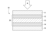
- FIG. 1 is a schematic cross-sectional view illustrating an example of an embodiment of an organic photoelectric conversion element of the present invention.
- 1 is a microscopic image of the film surface of the organic photoelectric conversion film obtained in Example 1 after a heat resistance test.
- 1 is a microscopic image of the film surface of the organic photoelectric conversion film obtained in Example 2 after a heat resistance test.
- 1 is a microscopic image of the film surface of the organic photoelectric conversion film obtained in Example 3 after a heat resistance test.
- 1 is a microscopic image of the film surface of the organic photoelectric conversion film obtained in Example 4 after a heat resistance test.
- 1 is a microscopic image of the film surface of the organic photoelectric conversion film obtained in Comparative Example 1 after a heat resistance test.
- the "total solid content of the organic semiconductor ink composition” refers to all components in the organic semiconductor ink composition other than the solvent. Even if a component other than the solvent is liquid at room temperature, that component is not included in the solvent but is included in the total solid content.
- the numerical range expressed using "to” means a range including the numerical values before and after "to" as the lower and upper limits.
- the organic photoelectric conversion film of this embodiment contains a p-type organic semiconductor and an n-type organic semiconductor.
- the p-type organic semiconductor is not particularly limited and any known compound can be used, preferably a donor organic semiconductor (compound).
- the p-type organic semiconductor is preferably a polymer compound.
- a hole-transporting organic compound that is a p-type conjugated polymer compound can be mentioned, and a polymer compound that has the property of easily donating electrons can be used.
- the polymer compound means a polymer having a molecular weight distribution and a weight average molecular weight of 10,000 or more in terms of standard polystyrene, determined by size exclusion chromatography.
- the p-type organic semiconductor is preferably a compound having a skeleton with excellent hole transport properties.
- skeletons having excellent hole transport properties include a carbazole structure, a thiophene structure, a benzodithiophene structure, a thienothiophene structure, a dibenzofuran structure, a triarylamine structure, a naphthalene structure, a phenanthrene structure, and a pyrene structure.
- Compounds that can form a film by mixing with an n-type organic semiconductor to be described later and applying the mixture are preferred.
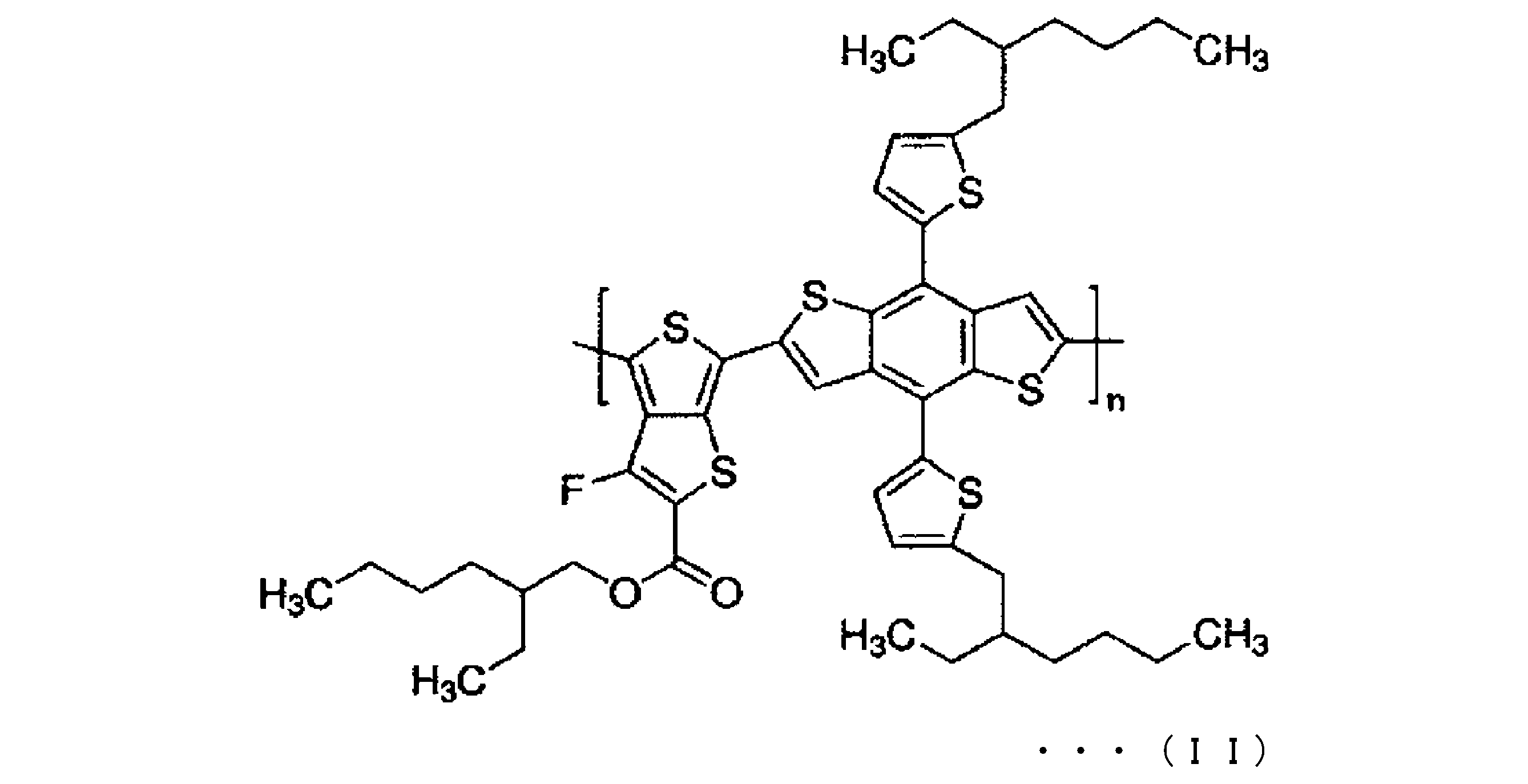
- the p-type organic semiconductor is preferably a polymer compound containing a repeating structure represented by the following formula (II):
- n is a positive integer.
- the polymer compound containing the repeating unit represented by formula (II) may be a compound described in Japanese Patent No. 5898782, or may be a compound commercially available from 1-material or Sigma-Aldrich.
- the weight average molecular weight of the p-type organic semiconductor used in this embodiment is preferably 10,000 or more, more preferably 50,000 or more, since the characteristics as a p-type semiconductor are easily expressed.
- the upper limit is preferably 150,000, more preferably 100,000, from the viewpoint of solubility in a solvent.
- the above upper and lower limits can be arbitrarily combined. For example, it may be 10,000 to 150,000, or 50,000 to 100,000.
- the weight average molecular weight of the p-type organic semiconductor is a value determined by size exclusion chromatography.
- the n-type organic semiconductor is an acceptor semiconductor, and is mainly represented by an electron transporting compound, which is a compound that has a tendency to accept electrons. More specifically, it refers to the compound that has a larger electron affinity when two compounds are used in contact with each other. Therefore, any compound that has electron accepting properties can be used as the acceptor compound.
- the n-type organic semiconductor is an organic compound with a molecular weight of 500 to 5000.
- the molecular weight is more preferably 800 to 4000, and even more preferably 1000 to 3000. If the molecular weight is equal to or greater than the lower limit, the compound has excellent ability to form a BHJ structure with the p-type organic semiconductor, and if the molecular weight is equal to or less than the upper limit, the compound has excellent solubility in a solvent.
- n-type organic semiconductors include condensed aromatic carbocyclic compounds (naphthalene derivatives, anthracene derivatives, phenanthrene derivatives, tetracene derivatives, pyrene derivatives, perylene derivatives, fluoranthene derivatives, etc.), 5- to 7-membered heterocyclic compounds containing a nitrogen atom, an oxygen atom, or a sulfur atom (e.g., pyridine, pyrazine, pyrimidine, pyridazine, triazine, quinoline, quinoxaline, quinazoline, phthalazine, cinnoline, isoquinoline, pteridine, acridine, phenazine, phenanthroline, tetrazole, pyrazole, imidazoline, tetrazole, pyrazole ...
- condensed aromatic carbocyclic compounds naphthalene derivatives, anthracene derivatives, phen
- the metal complexes include those having a ligand such as an aryl azole, thiazole, oxazole, indazole, benzimidazole, benzotriazole, benzoxazole, benzothiazole, carbazole, purine, triazolopyridazine, triazolopyrimidine, tetrazaindene, oxadiazole, imidazopyridine, pyrazine, pyrrolopyridine, thiadiazolopyridine, dibenzazepine, tribenzazepine, etc.), a polyarylene compound, a fluorene compound, a cyclopentadiene compound, a silyl compound, or a nitrogen-containing heterocyclic compound.
- a ligand such as an aryl azole, thiazole, oxazole, indazole, benzimidazole, benzotriazole, benzoxazole, benzothiazole, carbazole, pur
- the content ratio of the n-type organic semiconductor having a fullerene skeleton is 0 to 10 parts by mass, preferably 0 to 5 parts by mass, and more preferably 0 to 2 parts by mass, per 100 parts by mass of the n-type organic semiconductor not having a fullerene skeleton.
- the n-type organic semiconductor is preferably a fullerene skeleton-free semiconductor that does not substantially contain an n-type organic semiconductor having a fullerene skeleton.
- substantially not containing an n-type organic semiconductor having a fullerene skeleton means that the n-type organic semiconductor having a fullerene skeleton is not responsible for transporting electrons of the charges generated in the photoelectric conversion layer, and it is permissible to contain a small amount of an n-type organic semiconductor having a fullerene skeleton in order to improve the morphology of the photoelectric conversion layer.
- the content ratio of the n-type organic semiconductor having a fullerene skeleton may be 5 parts by mass or less, or 2 parts by mass or less, relative to 100 parts by mass of the content of the n-type organic semiconductor not having a fullerene skeleton.
- the n-type organic semiconductor used in this embodiment preferably contains a compound represented by the following formula (I), particularly from the viewpoint of compatibility with p-type organic semiconductors and ability to form a BHJ-type photoelectric conversion layer.
- A represents an atom selected from Group 14 of the periodic table
- X 1 to X 4 each independently represent a hydrogen atom or a halogen atom
- R 1a and R 1b each independently represent a linear or branched alkyl group
- R 2 to R 5 each independently represent a linear or branched alkyl group, a linear or branched alkoxy group, a linear or branched thioalkyl group, or a hydrogen atom.
- A is preferably a carbon atom or a silicon atom.
- X 1 to X 4 each independently represent a hydrogen atom or a halogen atom, and the halogen atom is preferably a fluorine atom or a chlorine atom.
- R 1a and R 1b each independently represent a linear or branched alkyl group, and the alkyl group preferably has 4 to 24 carbon atoms, more preferably 6 to 16 carbon atoms, and even more preferably 8 to 12 carbon atoms.
- linear or branched alkyl groups having 8 to 24 carbon atoms include linear alkyl groups such as n-octyl, n-decyl, lauryl, myristyl, palmityl, and stearyl; primary alkyl groups having branches such as 2-ethylhexyl and 2-butyloctyl; and secondary alkyl groups such as 2-octyl, 2-nonyl, and 2-decyl.
- Linear alkyl groups and primary alkyl groups having branches are preferred, with 2-ethylhexyl and 2-butyloctyl being more preferred.
- R 2 to R 5 are each independently a linear or branched alkyl group, a linear or branched alkoxy group, a linear or branched thioalkyl group, or a hydrogen atom, and the alkyl group, alkoxy group, and thioalkyl group preferably have 4 to 24 carbon atoms, more preferably 4 to 16 carbon atoms, and even more preferably 6 to 12 carbon atoms.
- Each of R2 and R3 is preferably an alkyl group or alkoxy group having 6 to 12 carbon atoms, and each of R4 and R5 is preferably a hydrogen atom.
- R 1a and R 1b are the same group, it is preferable that R 2 and R 3 are different groups selected from an alkyl group and an alkoxy group, and it is desirable that R 4 and R 5 are each a hydrogen atom.
- ⁇ Content ratio of p-type organic semiconductor and n-type organic semiconductor> The present inventors have found that one of the parameters related to the thermal stability of an organic photoelectric conversion film is the ratio of a p-type organic semiconductor to an n-type organic semiconductor in the organic photoelectric conversion film.
- the ratio of the p-type organic semiconductor to the n-type organic semiconductor in the organic photoelectric conversion film of this embodiment may be 0.2 to 2.0, may be 0.2 to 1.8, may be 0.2 to 1.6, may be 0.25 to 1.5, may be 0.25 to 1.4, or may be 0.3 to 1.2.
- the thermal stability of the organic photoelectric conversion film is likely to be improved, and an organic photoelectric conversion film having a small surface roughness Ra after a heat resistance test is likely to be obtained.
- the n-type organic semiconductor is relatively more, the organic photoelectric conversion element characteristics tend to be improved.
- the organic photoelectric conversion film of the present embodiment may contain other components as necessary in addition to the above-mentioned p-type organic semiconductor and n-type organic semiconductor.
- the organic photoelectric conversion film when the organic photoelectric conversion film is a film obtained by solidifying a coating of an organic semiconductor ink composition (hereinafter also simply referred to as "ink composition") described below, the organic photoelectric conversion film may contain components derived from the ink composition. Examples of other components include stabilizers, viscosity modifiers, curing agents, and high-boiling point additives described below.
- the total content of other components contained in the organic photoelectric conversion film of this embodiment is preferably 10 mass% or less, more preferably 5 mass% or less, even more preferably 2 mass% or less, and particularly preferably 1 mass% or less, based on 100 mass% of the mass of the organic photoelectric conversion film. That is, the total content of the p-type organic semiconductor and the n-type organic semiconductor in the organic photoelectric conversion film of this embodiment is preferably 90 to 100 mass%, more preferably 95 to 100 mass%, still more preferably 98 to 100 mass%, and particularly preferably 99 to 100 mass%, based on 100 mass% of the mass of the organic photoelectric conversion film.
- the organic photoelectric conversion film of this embodiment has a surface roughness Ra after a heat resistance test of 0.1 to 10 nm, preferably 0.1 to 5 nm, and more preferably 0.1 to 2 nm.
- the heat resistance test is performed using a sample having a film thickness of 50 to 500 nm, by holding the sample for 50 minutes at a temperature of 200° C. in a nitrogen atmosphere (an atmosphere in which the water vapor and oxygen concentrations are controlled to 10 ppm or less) in a dark place without actively irradiating the sample with ultraviolet light, visible light, infrared light, etc.
- the organic photoelectric conversion film of this embodiment has a surface roughness Ra of 0.1 to 10 nm, preferably 0.1 to 5 nm, and more preferably 0.1 to 2 nm after the heat resistance test.
- the temperature condition of the heat resistance test being T°C means that the temperature of the organic photoelectric conversion film is T°C.
- the surface roughness Ra after the heat resistance test can be used as an index of the thermal stability of the organic photoelectric conversion film.
- the heat resistance test when the domains of the p-type organic semiconductor and the n-type organic semiconductor constituting the organic photoelectric conversion film are enlarged or crystallized, the smoothness of the surface of the organic photoelectric conversion film is impaired, and the surface roughness Ra increases.
- the smaller the difference in surface roughness Ra before and after the heat resistance test the more the film quality deterioration due to heating is suppressed.
- it is important that the surface roughness Ra after the heat resistance test is generally small.
- the thermal stability of the organic photoelectric conversion film it is possible to increase the heat resistance of an organic photoelectric conversion element including the organic photoelectric conversion film.
- an organic photoelectric conversion element in which the film quality of the organic photoelectric conversion layer is not easily deteriorated even after a reflow process during element production.
- the ratio of the p-type organic semiconductor to the n-type organic semiconductor contained in the organic photoelectric conversion film, i.e., in the ink composition, the selection of the type of solvent in the ink composition, and the type and amount of additives contained in the ink composition can be factors that determine the surface roughness Ra of the organic photoelectric conversion film after a heat resistance test.
- the method for producing an organic photoelectric conversion film of this embodiment includes a step of forming a coating film by applying an ink composition containing a p-type organic semiconductor, an n-type organic semiconductor, and a solvent, and a step of obtaining an organic photoelectric conversion film by solidifying the coating film. That is, the method for producing an organic photoelectric conversion film of this embodiment includes forming a coating film by applying an ink composition containing a p-type organic semiconductor, an n-type organic semiconductor, and a solvent, and forming an organic photoelectric conversion film by solidifying the formed coating film. Specifically, the ink composition is applied to a coating target to form a coating film (unsolidified film), and then the solvent in the coating film is removed to form a solidified film of the ink composition (organic photoelectric conversion film).
- the method for forming a coating of the ink composition may be a known wet film-forming method such as spin coating.
- the conditions for spin coating may be appropriately set according to a standard method, taking into account the viscosity of the ink composition, etc.
- the solvent in the coating film can be removed by a known method such as heat drying or reduced pressure drying.
- the solvent contained in the ink composition of this embodiment may be any solvent that can dissolve the p-type organic semiconductor and the n-type organic semiconductor.
- aromatic hydrocarbon solvents such as toluene, xylene, mesitylene, and cyclohexylbenzene
- Aromatic solvents such as aromatic halogen-containing solvents such as chlorobenzene and o-dichlorobenzene
- Aliphatic halogen-containing solvents such as 1,2-dichloroethane
- Aliphatic ethers such as ethylene glycol dimethyl ether, ethylene glycol diethyl ether, and propylene glycol-1-monomethyl ether acetate (PGMEA)
- Ether solvents such as aromatic ethers such as 1,2-dimethoxybenzene, 1,3-dimethoxybenzene, anisole, phenetole, 2-methoxytoluene, 3-methoxytoluene, 4-methoxytoluene, 2,
- aromatic hydrocarbon solvents are preferred from the viewpoint of the solubility of p-type organic semiconductors and n-type organic semiconductors.
- Examples of the p-type organic semiconductor and n-type organic semiconductor used in the ink composition of this embodiment include the compounds described above as the p-type organic semiconductor and n-type organic semiconductor used in the organic photoelectric conversion film.
- the n/p ratio in the ink composition of this embodiment can be considered to be the same as the n/p ratio in the organic photoelectric conversion film.
- examples of the other components used in the ink composition include the components described above as the other components used in the organic photoelectric conversion film.
- the total content of other components in the total solid content of the ink composition of this embodiment, and the total content of the p-type organic semiconductor and the n-type organic semiconductor can be considered to be the same as the content in the organic photoelectric conversion film.
- the solids concentration of the ink composition of this embodiment i.e., the total solids content excluding the solvent from the ink composition, is preferably 10 to 40 mg/mL, and more preferably 15 to 30 mg/mL. If it is equal to or higher than the lower limit, the film-forming properties of the photoelectric conversion layer are excellent, and if it is equal to or lower than the upper limit, the ink composition can be easily prepared and is easy to handle.
- the high-boiling point additive partially dissolves either or both of the p-type organic semiconductor and the n-type organic semiconductor when the ink composition is applied and dried, thereby maintaining the fluidity of these, and assisting in the formation of a bulk heterojunction that is expected to exhibit high performance as an organic photoelectric conversion film.
- the boiling point of the high-boiling additive is 200° C. or higher, and although there is no particular upper limit, it is usually 350° C. or lower.
- the molecular weight of the high boiling point additive is less than 500, preferably 50 to 400, and more preferably 100 to 300. Examples of the high boiling point additive include naphthalene-based compounds.
- the naphthalene-based compounds are not particularly limited, and examples thereof include 1-phenylnaphthalene (boiling point: 320° C.), 1-methylnaphthalene (boiling point: 241° C.), 1-ethylnaphthalene (boiling point: 260° C.), 1-chloronaphthalene (boiling point: 263° C.), 1-bromonaphthalene (boiling point: 282° C.), and 1-fluoronaphthalene (boiling point: 212° C.).
- Organic photoelectric conversion element of the present embodiment has a photoelectric conversion layer which is the organic photoelectric conversion film of the present embodiment described above.
- the structure of the organic photoelectric conversion element of this embodiment can be, for example, as described in JP 2007-324587 A, and is not particularly limited.
- the organic photoelectric conversion element may have a structure in which a transparent electrode, an electron transport layer, a photoelectric conversion layer, a hole transport layer, and a metal electrode are laminated in this order on a transparent substrate, or a structure in which a transparent electrode, a hole transport layer, a photoelectric conversion layer, an electron transport layer, and a metal electrode are laminated in this order on a transparent substrate.
- FIG. 1 is a schematic cross-sectional view showing an example of an organic photoelectric conversion element of this embodiment.
- this organic photoelectric conversion element 10 a first electrode 11, a hole transport layer 12, a photoelectric conversion layer 13, an electron transport layer 14, and a second electrode 15 as a lower electrode are laminated in this order.
- the hole transport layer 12, the photoelectric conversion layer 13, and the electron transport layer 14 form an organic photoelectric film 20.
- a substrate is provided on the side of the first electrode 11 opposite the hole transport layer 12.
- the organic photoelectric conversion element may include a substrate to support the first electrode, the hole transport layer, the photoelectric conversion layer, the electron transport layer, the second electrode, etc.
- the substrate may be provided on either the first electrode side or the second electrode side, or on both sides, but is preferably provided at least on the first electrode side.
- the substrate can be made of any material, but if light is incident from the substrate side, it must be made of a highly transparent material.
- materials constituting the substrate include inorganic materials such as glass, sapphire, and titania; organic materials such as polyethylene terephthalate, polyethylene naphthalate, polyethersulfone, polyimide, nylon, polystyrene, polyvinyl alcohol, ethylene-vinyl alcohol copolymer, fluororesin, vinyl chloride, polyethylene, cellulose, polyvinylidene chloride, aramid, polyphenylene sulfide, polyurethane, polycarbonate, polyarylate, and polynorbornene; paper materials such as paper and synthetic paper; and composite materials such as metals such as stainless steel, titanium, and aluminum whose surfaces are coated or laminated to impart insulating properties.
- the constituent materials of the substrate may be used alone or in combination of two or more.
- the substrate may have another layer laminated thereon in order to impart gas barrier properties or control the surface condition.
- the thickness of the substrate can be freely designed depending on the application and constituent materials of the organic photoelectric conversion element, but a thicker substrate is preferable in terms of strength as a support member, while a thinner substrate is preferable in terms of cost. Therefore, a film- or plate-shaped substrate with a thickness of about 10 ⁇ m to 50 mm is usually used.
- the electrodes (first electrode, second electrode) can be made of any material having electrical conductivity.
- Examples of materials constituting the electrodes include metals such as platinum, gold, silver, aluminum, chromium, nickel, copper, titanium, magnesium, calcium, barium, and sodium, or alloys thereof; metal oxides such as indium oxide and tin oxide, or composite oxides thereof (e.g., ITO and IZO); conductive polymers such as polyaniline, polypyrrole, polythiophene, and polyacetylene; conductive polymers to which dopants such as acids such as hydrochloric acid, sulfuric acid, and sulfonic acid, Lewis acids such as FeCl3 , halogen atoms such as iodine, and metal atoms such as sodium and potassium have been added; and conductive composite materials in which conductive particles such as metal particles, carbon black, fullerene, and carbon nanotubes are dispersed in a matrix such as a polymer binder.
- the electrode may be made of one material alone or two or more materials in combination.
- an organic photoelectric conversion element at least one pair (two electrodes) is provided, and a photoelectric conversion layer is provided between the pair of electrodes.
- at least one of the pair of electrodes is transparent (i.e., transmits light absorbed by the photoelectric conversion layer for power generation).
- transparent electrodes include complex oxides such as indium tin oxide (ITO) and indium zinc oxide (IZO); and thin metal films.
- ITO indium tin oxide
- IZO indium zinc oxide
- thin metal films There is no specific limit to the range of light transmittance, but considering the photoelectric conversion efficiency of the organic photoelectric conversion element, 80% or more is preferable. Light transmittance can be measured with a normal spectrophotometer.
- the electrode has a function of collecting holes and electrons generated in the photoelectric conversion layer, and therefore, as a material for the electrode, it is preferable to use a material suitable for collecting holes and electrons from among the above-mentioned materials.
- electrode materials suitable for collecting holes include materials having a high work function, such as Au and ITO.
- Electrode materials suitable for collecting electrons include materials with low work functions, such as aluminum (Al).
- the thickness of the electrodes there are no particular limitations on the thickness of the electrodes, and it is determined appropriately taking into consideration the material used and the required conductivity, transparency, etc., but it is usually around 10 nm to 100 ⁇ m.
- the method for forming the electrodes is not limited, but they can be formed by a dry process such as vacuum deposition or sputtering. They can also be formed by a wet process using a conductive ink composition. Any conductive ink composition can be used, such as a conductive polymer or a metal particle dispersion.
- the electrodes can be laminated in two or more layers, and can be surface-treated to improve their properties (e.g., electrical properties, wettability).
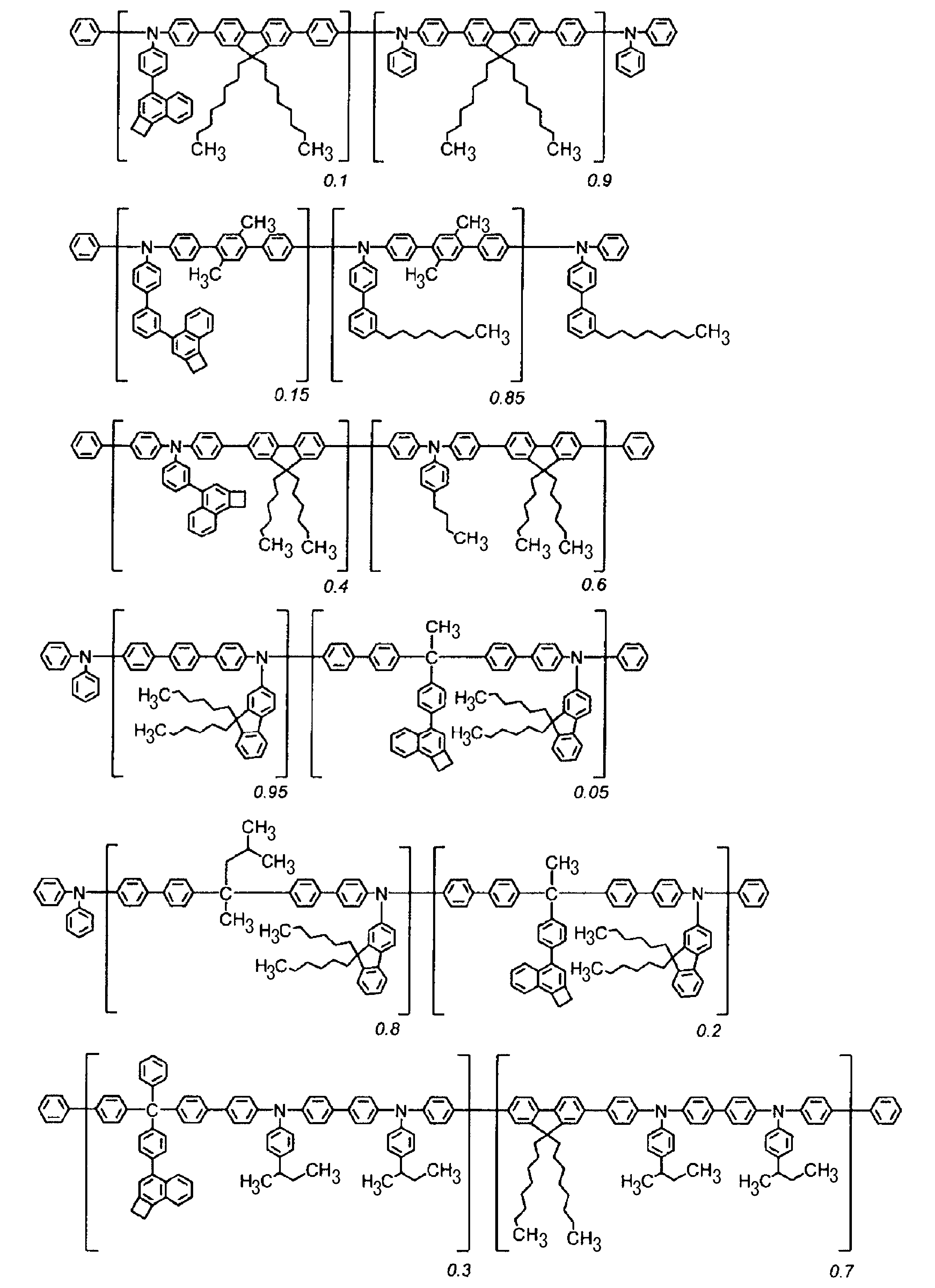
- the hole transport layer may be made of a known hole transport material, including, but not limited to, a hole transport polymer such as a polytriarylamine compound represented by the following chemical formula:
- a hole transport polymer such as a polytriarylamine compound represented by the following chemical formula:
- 2,7-bis (4-bromophenyl) -9,9-dihexylfluorene described in JP 2019-173032 A 2-amino-9,9-dihexylfluorene
- 4- 4- (1,1-bis (4'-bromo- [1,1'-biphenyl] -4-yl) ethyl) phenyl) -1,2-dihydrocyclobuta [a] naphthalene synthesized polytolyl arylamine compound
- 4,4'-dibromobiphenyl 2-amino-9,9-dihexylfluorene
- the method for forming the hole transport layer is not particularly limited, but it is preferably formed by a wet film formation method using a hole transporting polymer.
- a composition for forming the hole transport layer containing a hole transporting polymer and a solvent is used.
- the solvent in the composition for forming the hole transport layer is sufficient if it dissolves the hole transport polymer, and is a solvent that dissolves the hole transport polymer at room temperature in an amount of 0.05% by mass or more, preferably 0.5% by mass or more, and more preferably 1% by mass or more.
- ether-based solvents, ester-based solvents, aromatic hydrocarbon-based solvents, and amide-based solvents are preferred.
- ether solvents include aliphatic ethers such as ethylene glycol dimethyl ether, ethylene glycol diethyl ether, and propylene glycol-1-monomethyl ether acetate (PGMEA); and aromatic ethers such as 1,2-dimethoxybenzene, 1,3-dimethoxybenzene, anisole, phenetole, 2-methoxytoluene, 3-methoxytoluene, 4-methoxytoluene, 2,3-dimethylanisole, and 2,4-dimethylanisole.
- aliphatic ethers such as ethylene glycol dimethyl ether, ethylene glycol diethyl ether, and propylene glycol-1-monomethyl ether acetate (PGMEA)
- aromatic ethers such as 1,2-dimethoxybenzene, 1,3-dimethoxybenzene, anisole, phenetole, 2-methoxytoluene, 3-methoxytoluene, 4-meth
- ester solvent examples include aromatic esters such as phenyl acetate, phenyl propionate, methyl benzoate, ethyl benzoate, propyl benzoate, and n-butyl benzoate.
- aromatic hydrocarbon solvents include toluene, xylene, cyclohexylbenzene, 3-isopropylbiphenyl, 1,2,3,4-tetramethylbenzene, 1,4-diisopropylbenzene, cyclohexylbenzene, and methylnaphthalene.
- amide solvent examples include N,N-dimethylformamide and N,N-dimethylacetamide, and dimethylsulfoxide can also be used.
- the concentration of the hole transport polymer in the composition for forming the hole transport layer can be any concentration as long as it does not significantly impair the effect of this embodiment.
- a lower concentration is preferable in terms of uniformity of the film thickness, while a higher concentration is preferable in terms of preventing defects from occurring in the hole transport layer.
- the concentration is preferably 0.01% by mass or more, more preferably 0.1% by mass or more, and even more preferably 0.5% by mass or more, and is preferably 70% by mass or less, more preferably 60% by mass or less, and even more preferably 50% by mass or less.
- the concentration of the solvent in the composition for forming the hole transport layer is usually 10% by mass or more, preferably 30% by mass or more, and more preferably 50% by mass or more.
- the composition for forming a hole transport layer is usually heated after coating.
- the heating method is not particularly limited, but in the case of drying by heating, the layer formed using the composition for forming a hole transport layer is usually heated to 100° C. or higher, preferably 120° C. or higher, more preferably 150° C. or higher, and usually 400° C. or lower, preferably 350° C. or lower, more preferably 300° C. or lower.
- the heating time is usually 1 minute or more, preferably 24 hours or less.
- the heating means is not particularly limited, but the laminate having the formed layer may be placed on a hot plate or heated in an oven. For example, the heating condition may be 120° C. or more on a hot plate for 1 minute or more.
- the thickness of the hole transport layer is 50 nm or more and 100 nm or less, and in another embodiment, it is more than 100 nm and 400 nm or less, preferably 350 nm or less, i.e., 50 nm or more and 400 nm or less, preferably 50 nm or more and 350 nm or less.
- the thickness of the hole transport layer is preferably thick in that the effect of reducing dark current due to the provision of the hole transport layer as a blocking layer is easily achieved, and is preferably thin in that the angle of incidence of light can be made wide in a CMOS image sensor using an organic photoelectric conversion element and the organic photoelectric conversion element can be made thin.
- the hole transport layer preferably has a LUMO (lowest unoccupied molecular orbital) that is shallower by 0.3 eV or more than the n-type organic semiconductor of the photoelectric conversion layer, more preferably has a LUMO that is shallower by 0.5 eV or more, and even more preferably has a LUMO that is shallower by 1.0 eV or more.
- the difference in HOMO (highest occupied molecular orbital) between the hole transport layer and the p-type organic semiconductor of the photoelectric conversion layer is preferably within 0.5 eV, and more preferably within 0.3 eV.
- the photoelectric conversion layer is a layer that absorbs light and separates electric charges.
- the thickness of the photoelectric conversion layer can be arbitrarily designed depending on the configuration of the photoelectric conversion layer and the use of the organic photoelectric conversion element, but is preferably 10 nm to 1 ⁇ m. If it is equal to or more than the lower limit, light absorption is sufficient and efficiency is likely to be high, and if it is equal to or less than the upper limit, internal resistance is reduced and loss is likely to be small.
- the photoelectric conversion layer of the organic photoelectric conversion element of the present embodiment can usually be formed by a method in which the above-described ink composition is applied onto a carrier transport layer (a hole transport layer or an electron transport layer) to form a coating film, and then the coating film is solidified.
- a carrier transport layer a hole transport layer or an electron transport layer
- an electron transport layer may be provided between the photoelectric conversion layer and the second electrode in order to increase the photoelectric conversion efficiency and easily reduce dark current.
- the electron transport layer is formed from a compound capable of efficiently transporting electrons generated in the photoelectric conversion layer to the second electrode.
- the electron transporting compound used in the electron transport layer is required to have a high efficiency of electron injection from the photoelectric conversion layer and a high electron mobility so as to efficiently transport the injected electrons.
- the difference in LUMO between the electron transport layer and the n-type organic semiconductor of the photoelectric conversion layer is preferably 1.5 eV or less, and more preferably 1.0 eV or less.
- the electron transport layer when dark current is reduced by the electron transport layer, preferably has a HOMO that is 0.3 eV or more deeper than the p-type semiconductor of the photoelectric conversion layer, more preferably has a HOMO that is 0.5 eV or more deeper, and even more preferably has a HOMO that is 1.0 eV or more deeper.
- electron transport compounds used in the electron transport layer include metal complexes such as aluminum complexes of 8-hydroxyquinoline (JP Patent Publication 59-194393), metal complexes of 10-hydroxybenzo[h]quinoline, oxadiazole derivatives, distyrylbiphenyl derivatives, silole derivatives, 3-hydroxyflavone metal complexes, 5-hydroxyflavone metal complexes, benzoxazole metal complexes, benzothiazole metal complexes, trisbenzimidazolylbenzene (US Patent Publication 5,645,948), quinoxaline compounds (JP Patent Publication 6-207169), phenanthroline derivatives (JP Patent Publication 5-331459), 2-t-butyl-9,10-N,N'-dicyanoanthraquinone diimine, n-type hydrogenated amorphous silicon carbide, n-type zinc sulfide, and n-type zinc selenide.
- metal complexes such as aluminum complexe
- Metal oxides such as titanium oxide, zinc oxide, tin oxide, and cerium oxide can also be used as materials for forming the electron transport layer.
- the method for forming the electron transport layer can be a method of wet-forming nanoparticles of the metal oxide and drying them to form a metal oxide layer, or a method of wet-forming a precursor and converting it by heating.
- the thickness of the electron transport layer is usually 1 nm or more, preferably 5 nm or more, and usually 300 nm or less, preferably 100 nm or less.
- the above upper and lower limits can be combined in any way. For example, it may be 1 to 300 nm, or 5 to 100 nm.
- the electron transport layer can be formed by a wet deposition method or a vacuum deposition method, but the vacuum deposition method is usually used.
- the organic photoelectric conversion element may include constituent layers other than the above-described substrate, first and second electrodes, hole transport layer, photoelectric conversion layer, and electron transport layer, as long as the effects of this embodiment are not significantly impaired.
- the organic photoelectric conversion element may be provided with a protective film to cover the photoelectric conversion layer portion and further the electrode portion in order to minimize the influence of the outside air.
- the protective layer may be composed of, for example, a polymer film such as a styrene resin, an epoxy resin, an acrylic resin, a polyurethane, a polyimide, a polyvinyl alcohol, a polyvinylidene fluoride, a polyethylene-polyvinyl alcohol copolymer, or the like; an inorganic oxide film or a nitride film such as silicon oxide, silicon nitride, or aluminum oxide; or a laminated film thereof.
- a polymer film such as a styrene resin, an epoxy resin, an acrylic resin, a polyurethane, a polyimide, a polyvinyl alcohol, a polyvinylidene fluoride, a polyethylene-polyvinyl alcohol copolymer, or the like
- an inorganic oxide film or a nitride film such as silicon oxide, silicon nitride, or aluminum oxide
- the method for forming the protective film there are no limitations on the method for forming the protective film.
- the protective film when the protective film is a polymer film, examples of the method include a method of coating and drying a polymer solution, and a method of coating or evaporating a monomer and polymerizing it.
- a polymer film it is also possible to carry out a crosslinking process or form a multi-layer film.
- the protective film is an inorganic film such as an inorganic oxide film or a nitride film, for example, a vacuum process such as a sputtering method or a vapor deposition method, or a solution process such as the sol-gel method can be used.
- a charge injection layer may be provided between the first electrode and the hole transport layer, or between the electron transport layer and the second electrode.
- the organic photoelectric conversion element may be provided with an optical filter that does not transmit ultraviolet light on the light incident side, for example. Since ultraviolet light generally accelerates the deterioration of organic photoelectric conversion elements, blocking this ultraviolet light can extend the life of the organic photoelectric conversion element.
- a manufacturing method of an organic photoelectric conversion element having a first electrode, a hole transport layer, a photoelectric conversion layer, and a second electrode on a substrate in this order will be described as an example.
- the organic photoelectric conversion element is usually manufactured by laminating the first electrode, the hole transport layer, the photoelectric conversion layer, and the second electrode on a substrate in this order by the above-mentioned method.
- a forming process of an electron transport layer, etc., which is provided as necessary, is provided between these layers.
- the photoelectric conversion layer of the organic photoelectric conversion element may be subjected to a pretreatment such as a thermal annealing treatment or a solvent annealing treatment before the organic photoelectric conversion element is completed.
- the solvent annealing treatment is a treatment in which the photoelectric conversion layer is exposed to a specific solvent atmosphere, and can be carried out by a known method. It is preferable to subject the coating film to a thermal annealing treatment, which also serves as a drying treatment for removing the solvent in the coating film. The drying treatment and the thermal annealing treatment may be performed separately.
- the thermal annealing method include a method of directly heating using a hot plate, a hot air heating method, an infrared heating method, and a light heating method using a flash lamp.
- the outer surface of the carrier transport layer side (the surface opposite to the photoelectric conversion layer) of a laminate in which a photoelectric conversion layer is formed on a carrier transport layer can be heated by contacting it with a hot plate.
- the heating temperature in the thermal annealing treatment is preferably, for example, 80 to 300° C.
- the heating time in the thermal annealing treatment is preferably, for example, 1 second to 30 minutes.
- the heating temperature of the drying treatment or thermal annealing treatment of the photoelectric conversion layer being t°C means that the temperature of the photoelectric conversion layer is t°C.
- a preferred embodiment of the method for subjecting the organic photoelectric conversion film to a thermal annealing treatment is as follows.
- a thermal annealing treatment is carried out, which also serves as a drying treatment, immediately after the formation of a coating film of the ink composition.
- a coating film of the ink composition is formed, dried by a reduced pressure drying method to solidify the coating film, and then subjected to a thermal annealing treatment.
- a step of laminating a carrier transport layer (a hole transport layer or an electron transport layer) that is not deteriorated by the heat of the thermal annealing treatment on the solidified organic photoelectric conversion film can be provided.
- the photoelectric conversion element of this embodiment is used, for example, in an optical sensor or an image sensor.
- the optical sensor or image sensor may have a known configuration.
- the heat resistance test was a heating test simulating a heating environment such as that during a reflow process in element production, and was carried out under conditions in which the organic photoelectric conversion element was held at a temperature of 200° C. for 50 minutes.
- Example 1 [Formation of Hole Transport Layer] A surface of an ITO substrate having a pattern of a transparent conductive film of indium tin oxide (ITO) formed as an electrode on a glass substrate was treated with an ultraviolet ozone cleaner (NL-UV253, manufactured by Japan Laser Electronics Co., Ltd.) for 10 minutes, and then a hole transport layer was formed as follows.
- ITO indium tin oxide
- a polytriarylamine compound (hole transport polymer) shown in the following formula (1) was dissolved in 1 mL of anisole to prepare a composition for forming a hole transport layer.
- This composition was spin-coated on the electrode surface of the ITO substrate at a rotation speed of 1000 rpm for 60 seconds, and then heated and dried at 240°C for 30 minutes to form a hole transport layer with a thickness of 300 nm.
- the p-type organic semiconductor used was the compound represented by the above formula (II) (weight average molecular weight: 80,000).
- the n-type organic semiconductor used was a compound (molecular weight 1339) of the above formula (I) in which A is a carbon atom, X 1 to X 4 are each a chlorine atom, R 1a and R 1b are each a 2-ethylhexyl group, R 2 is a 2-ethylhexyl group, R 3 is a 2-ethylhexyloxy group, and R 4 and R 5 are each a hydrogen atom.
- An organic semiconductor ink composition was prepared by dissolving 0.11 g of a p-type organic semiconductor and 0.03 g of an n-type organic semiconductor in 9.68 mL of o-xylene.
- the n/p ratio was 0.3
- the solid concentration of the organic semiconductor ink composition was 14 mg/mL.
- the obtained organic semiconductor ink composition was spin-coated onto the hole transport layer at 1000 revolutions per minute, and then heat-treated (thermal annealing treatment) at 120° C. for 10 minutes to form a photoelectric conversion layer.
- FIG. 2 shows a micrograph of the surface of the photoelectric conversion layer (organic photoelectric conversion film) after the heat resistance test observed with a scanning probe microscope (hereinafter simply referred to as "micrograph of the surface of the organic photoelectric conversion film").
- Example 2 An organic photoelectric conversion element was produced in the same manner as in Example 1, except that the amount of the n-type organic semiconductor used was changed to 0.07 g.
- the n/p ratio of the photoelectric conversion layer and the surface roughness Ra of the photoelectric conversion layer are shown in Table 1, and a microscope image of the surface of the organic photoelectric conversion film is shown in FIG.
- Example 3 An organic photoelectric conversion element was produced in the same manner as in Example 1, except that the amount of the n-type organic semiconductor used was changed to 0.10 g.
- the n/p ratio of the photoelectric conversion layer and the surface roughness Ra of the photoelectric conversion layer are shown in Table 1, and a microscope image of the surface of the organic photoelectric conversion film is shown in FIG.
- Example 4 An organic photoelectric conversion element was produced in the same manner as in Example 1, except that the amount of the n-type organic semiconductor used was changed to 0.13 g.
- the n/p ratio of the photoelectric conversion layer and the surface roughness Ra of the photoelectric conversion layer are shown in Table 1, and a microscope image of the surface of the organic photoelectric conversion film is shown in FIG.
- the surface roughness Ra of the organic photoelectric conversion layer after the heat resistance test was 0.8 to 1.2 nm in Examples 1 to 4.
- the surface roughness Ra of the organic photoelectric conversion layer after the heat resistance test in Comparative Example 1 was 25.1 nm. Since the organic photoelectric conversion films of Examples 1 to 4 have a small surface roughness Ra after the heat resistance test, it is expected that practical problems such as characteristic variations between pixels of an image sensor and poor image output are unlikely to occur.
- Comparative Example 1 since the n-type organic semiconductor was in excess relative to the p-type organic semiconductor, the compatibility between the two was insufficient, and it is believed that the excess n-type organic semiconductors aggregated and crystallized during the heat resistance test process, resulting in the large surface roughness Ra.
- Example 4 it is believed that the excess amount of the n-type organic semiconductor was appropriately suppressed, thereby suppressing aggregation and crystallization of the n-type organic semiconductor, thereby improving the surface roughness.
- the surface roughness Ra was small and high smoothness was obtained. This is believed to be because the p-type organic semiconductor, which is a polymer compound, is less likely to crystallize than the n-type organic semiconductor.
Landscapes
- Physics & Mathematics (AREA)
- Electromagnetism (AREA)
- Photovoltaic Devices (AREA)
- Inks, Pencil-Leads, Or Crayons (AREA)
Abstract
有機光電変換素子の耐熱性を高めることができる有機光電変換膜を提供する。本発明の有機光電変換膜は、p型有機半導体及びn型有機半導体を含有し、前記n型有機半導体の分子量が500~5000であり、前記n型有機半導体は、フラーレン骨格を有さないn型有機半導体の含有量100質量部に対して、フラーレン骨格を有するn型有機半導体の含有割合が0~10質量部であり、200℃の温度条件に50分間保持する耐熱性試験後の表面粗さRaが0.1~10nmである。
Description
本発明は、有機光電変換膜、有機光電変換素子、有機光電変換膜の製造方法、及び有機半導体インク組成物に関する。
本願は、2022年10月5日に日本出願された特願2022-160986号に基づき優先権を主張し、その内容をここに援用する。
本願は、2022年10月5日に日本出願された特願2022-160986号に基づき優先権を主張し、その内容をここに援用する。
塗布成膜法による有機太陽電池や光センサ(光ダイオード)などの有機光電変換素子の作製は、低いエネルギーコストで柔軟性や近赤外線検出などの従来のシリコン光電変換素子にはない特徴を有する光電変換素子を作製する方法として研究が続けられている。これらの有機光電変換素子の一つの形態としては、下部電極の上に正孔輸送層、活性層(有機光電変換層)、電子輸送層、上部電極を順に配置する構成が知られている。
このような有機光電変換素子には、素子製造時のリフロー工程などの加熱環境に耐えうる耐熱性が必要とされる。例えば、素子製造時の加熱環境を想定した耐熱性試験を課した素子において、有機光電変換層の耐熱性不足に由来する特性低下が見られる場合がある。その一因として、有機光電変換層の膜質劣化が挙げられる。
p型有機半導体とn型有機半導体を含む有機光電変換膜中で、p型有機半導体とn型有機半導体は、それぞれナノメートルオーダーの共連続ドメイン(バルクヘテロジャンクション構造:BHJ構造)を形成している。この共連続ドメインの耐熱性は低く、加熱によって各ドメインの増長や各材料の結晶化が増長され、それによって有機光電変換層の表面の平滑性が損なわれ得る。このような有機光電変換層の膜質劣化は、イメージセンサの画素間の特性バラツキ、出画不良等の実用上の問題を引き起こす。
かかる背景のもと、有機光電変換膜の耐熱性を改善して、有機光電変換層の表面凹凸を抑制するために従来様々な検討がなされてきた。
p型有機半導体とn型有機半導体を含む有機光電変換膜中で、p型有機半導体とn型有機半導体は、それぞれナノメートルオーダーの共連続ドメイン(バルクヘテロジャンクション構造:BHJ構造)を形成している。この共連続ドメインの耐熱性は低く、加熱によって各ドメインの増長や各材料の結晶化が増長され、それによって有機光電変換層の表面の平滑性が損なわれ得る。このような有機光電変換層の膜質劣化は、イメージセンサの画素間の特性バラツキ、出画不良等の実用上の問題を引き起こす。
かかる背景のもと、有機光電変換膜の耐熱性を改善して、有機光電変換層の表面凹凸を抑制するために従来様々な検討がなされてきた。
例えば、非特許文献1では、ポリ(3-アルキルチオフェン)側鎖にPCBMを導入したブロック共重合体を用いることで、ポリ(3-アルキルチオフェン)/PCBM混合の有機光電変換膜と比較して、PCBMの結晶化に起因する有機光電変換層の表面凹凸を抑制できることが報告されている。
Chem.Commun.,2010,46,6723-6725頁
しかしながら、非特許文献1の手法は、特定の材料についての技術である。
本発明は前記事情に鑑みてなされたものであり非特許文献1に開示されたような特定材料を用いなくとも、また新たな有機半導体を開発しなくとも、有機光電変換素子の耐熱性を高めることができる有機光電変換膜、その製造方法、及びこのような有機光電変換膜を有する有機光電変換素子の提供を課題とする。
本発明は前記事情に鑑みてなされたものであり非特許文献1に開示されたような特定材料を用いなくとも、また新たな有機半導体を開発しなくとも、有機光電変換素子の耐熱性を高めることができる有機光電変換膜、その製造方法、及びこのような有機光電変換膜を有する有機光電変換素子の提供を課題とする。
本発明は以下の態様を有する。
[1]p型有機半導体及びn型有機半導体を含有する有機光電変換膜であって、
前記n型有機半導体の分子量が500~5000であり、
前記n型有機半導体は、フラーレン骨格を有さないn型有機半導体の含有量100質量部に対して、フラーレン骨格を有するn型有機半導体の含有割合が0~10質量部であり、
200℃の温度条件に50分間保持する耐熱性試験後の表面粗さRaが0.1~10nmである、有機光電変換膜。
[2]有機光電変換膜中における、前記p型有機半導体と前記n型有機半導体の合計含有量が90~100質量%である、[1]の有機光電変換膜。
[3]有機光電変換膜中における、前記p型有機半導体の含有量に対する前記n型有機半導体の含有量の質量比を表すn/p比が、0.2~1.8である、[1]又は[2]の有機光電変換膜。
[4][1]~[3]のいずれかの有機光電変換膜を有する、有機光電変換素子。
[5][1]~[3]のいずれかの有機光電変換膜の製造方法であって、
前記p型有機半導体と、前記n型有機半導体と、溶媒とを含む有機半導体インク組成物の塗布による塗膜の形成、及び
前記塗膜の固化による有機光電変換膜の形成を含む、有機光電変換膜の製造方法。
[6]前記溶媒が芳香族炭化水素系溶媒を含む、[5]の有機光電変換膜の製造方法。
[7]前記有機半導体インク組成物が高沸点添加剤を実質的に含まない、[5]又は[6]の有機光電変換膜の製造方法。
[8]p型有機半導体、n型有機半導体、及び溶媒を含有する有機半導体インク組成物であって、
前記n型有機半導体の分子量が500~5000であり、
前記n型有機半導体は、フラーレン骨格を有さないn型有機半導体の含有量100質量部に対して、フラーレン骨格を有するn型有機半導体の含有割合が0~10質量部であり
高沸点添加剤を実質的に含まない、有機半導体インク組成物。
[9]有機半導体インク組成物の全固形分中における、前記p型有機半導体と前記n型有機半導体の合計含有量が90~100質量%である、[8]の有機半導体インク組成物。
[10]有機半導体インク組成物中における、前記p型有機半導体の含有量に対する前記n型有機半導体の含有量の質量比を示すn/p比が、0.2~1.8である、[8]又は[9]の有機半導体インク組成物。
[11]有機半導体インク組成物の塗布による塗膜の形成、及び前記塗膜の固化により形成された膜の、200℃の温度条件に50分間保持する耐熱性試験後の表面粗さRaが0.1~10nmである、[8]~[10]のいずれかの有機半導体インク組成物。
本発明によれば、有機光電変換素子の耐熱性を高めることができる有機光電変換膜、及びその製造方法が提供できる。
本発明によれば、耐熱性の高い有機光電変換素子が提供できる。
本発明によれば、有機光電変換素子の耐熱性を高めることができる有機光電変換膜が得られる有機半導体インク組成物が提供できる。
本発明によれば、耐熱性の高い有機光電変換素子が提供できる。
本発明によれば、有機光電変換素子の耐熱性を高めることができる有機光電変換膜が得られる有機半導体インク組成物が提供できる。
以下に本発明を実施するための形態を詳細に説明するが、以下に記載する構成要件の説明は、本発明の実施態様の代表例であり、本発明はこれらの内容に限定されるものではない。
本発明において、「有機半導体インク組成物の全固形分」とは、有機半導体インク組成物における溶媒以外の全成分を意味する。溶媒以外の成分が常温で液体であっても、その成分は溶媒には含めず、全固形分に含める。
本発明において「~」を用いて表される数値範囲は、「~」の前後に記載される数値を下限値及び上限値として含む範囲を意味する。
本発明において、「有機半導体インク組成物の全固形分」とは、有機半導体インク組成物における溶媒以外の全成分を意味する。溶媒以外の成分が常温で液体であっても、その成分は溶媒には含めず、全固形分に含める。
本発明において「~」を用いて表される数値範囲は、「~」の前後に記載される数値を下限値及び上限値として含む範囲を意味する。
<有機光電変換膜>
本実施形態の有機光電変換膜は、p型有機半導体及びn型有機半導体を含有する。
本実施形態の有機光電変換膜は、p型有機半導体及びn型有機半導体を含有する。
<p型有機半導体>
p型有機半導体は、特に限定されず公知の化合物を用いることができる。好ましくはドナー性の有機半導体(化合物)である。
p型有機半導体は高分子化合物が好ましい、具体的には、例えば、p型共役高分子化合物である正孔輸送性有機化合物が挙げられ、電子を供与しやすい性質を有する高分子化合物を用いることができる。
本明細書において、高分子化合物とは分子量分布を有し、サイズ排除クロマトグラフィーにより求めた標準ポリスチレン換算の重量平均分子量が10000以上である重合体を意味する。
p型有機半導体は、特に限定されず公知の化合物を用いることができる。好ましくはドナー性の有機半導体(化合物)である。
p型有機半導体は高分子化合物が好ましい、具体的には、例えば、p型共役高分子化合物である正孔輸送性有機化合物が挙げられ、電子を供与しやすい性質を有する高分子化合物を用いることができる。
本明細書において、高分子化合物とは分子量分布を有し、サイズ排除クロマトグラフィーにより求めた標準ポリスチレン換算の重量平均分子量が10000以上である重合体を意味する。
p型有機半導体は、正孔輸送性に優れる骨格を有する化合物が好ましい。
正孔輸送性に優れる骨格としては、例えば、カルバゾール構造、チオフェン構造、ベンゾジチオフェン構造、チエノチオフェン構造、ジベンゾフラン構造、トリアリールアミン構造、ナフタレン構造、フェナントレン構造、ピレン構造が挙げられる。後述するn型有機半導体と混合して塗布する方法で膜を形成できる化合物が好ましい。
正孔輸送性に優れる骨格としては、例えば、カルバゾール構造、チオフェン構造、ベンゾジチオフェン構造、チエノチオフェン構造、ジベンゾフラン構造、トリアリールアミン構造、ナフタレン構造、フェナントレン構造、ピレン構造が挙げられる。後述するn型有機半導体と混合して塗布する方法で膜を形成できる化合物が好ましい。
p型有機半導体は、具体的には、例えば、下記式(II)で表される繰り返し構造を含む高分子化合物が好適に用いられる。なお、式(II)中、nは正の整数である。
式(II)で表される繰り返し構造を含む高分子化合物は、日本国特許第5898782号に記載された化合物であってよく、また、1-material社やSigma-Aldrich社により市販されている化合物であってよい。
式(II)で表される繰り返し構造を含む高分子化合物は、日本国特許第5898782号に記載された化合物であってよく、また、1-material社やSigma-Aldrich社により市販されている化合物であってよい。
本実施形態で用いるp型有機半導体の重量平均分子量は、p型半導体としての特性が発現しやすいことから、10000以上が好ましく、50000以上がより好ましい。また上限は溶媒への溶解性の面から、150000が好ましく、100000がより好ましい。上記の上限及び下限は任意に組み合わせることができる。例えば、10000~150000であってよく、50000~100000であってよい。
前記重量平均分子量が高いと有機光電変換素子特性が高くなりやすく、また、一方で、低いと溶媒への溶解性に優れる。
本明細書において、p型有機半導体の重量平均分子量はサイズ排除クロマトグラフィーにより求めた値である。
前記重量平均分子量が高いと有機光電変換素子特性が高くなりやすく、また、一方で、低いと溶媒への溶解性に優れる。
本明細書において、p型有機半導体の重量平均分子量はサイズ排除クロマトグラフィーにより求めた値である。
<n型有機半導体>
n型有機半導体は、アクセプター性半導体であり、主に電子輸送性化合物に代表され、電子を受容しやすい性質がある化合物をいう。さらに詳しくは2つの化合物を接触させて用いたときに電子親和力の大きい方の化合物をいう。従って、アクセプター性化合物は、電子受容性のある化合物であればいずれの化合物も使用可能である。
n型有機半導体は、アクセプター性半導体であり、主に電子輸送性化合物に代表され、電子を受容しやすい性質がある化合物をいう。さらに詳しくは2つの化合物を接触させて用いたときに電子親和力の大きい方の化合物をいう。従って、アクセプター性化合物は、電子受容性のある化合物であればいずれの化合物も使用可能である。
本実施形態において、n型有機半導体は分子量が500~5000の有機化合物である。前記分子量は800~4000がより好ましく、1000~3000がさらに好ましい。前記下限値以上であればp型有機半導体とのBHJ構造形成能に優れ、また、前記上限値以下であれば溶媒への溶解性に優れる。
n型有機半導体としては、例えば、縮合芳香族炭素環化合物(ナフタレン誘導体、アントラセン誘導体、フェナントレン誘導体、テトラセン誘導体、ピレン誘導体、ペリレン誘導体、フルオランテン誘導体等)、窒素原子、酸素原子、硫黄原子を含有する5ないし7員のヘテロ環化合物(例えばピリジン、ピラジン、ピリミジン、ピリダジン、トリアジン、キノリン、キノキサリン、キナゾリン、フタラジン、シンノリン、イソキノリン、プテリジン、アクリジン、フェナジン、フェナントロリン、テトラゾール、ピラゾール、イミダゾール、チアゾール、オキサゾール、インダゾール、ベンズイミダゾール、ベンゾトリアゾール、ベンゾオキサゾール、ベンゾチアゾール、カルバゾール、プリン、トリアゾロピリダジン、トリアゾロピリミジン、テトラザインデン、オキサジアゾール、イミダゾピリジン、ピラリジン、ピロロピリジン、チアジアゾロピリジン、ジベンズアゼピン、トリベンズアゼピン等)、ポリアリーレン化合物、フルオレン化合物、シクロペンタジエン化合物、シリル化合物、含窒素ヘテロ環化合物を配位子として有する金属錯体が挙げられる。
これに限らず、上記したように、ドナー性半導体として用いた化合物よりも電子親和力の大きな化合物であればアクセプター性半導体として用いてよい。
これに限らず、上記したように、ドナー性半導体として用いた化合物よりも電子親和力の大きな化合物であればアクセプター性半導体として用いてよい。
n型有機半導体としてフラーレン骨格を有するものを用いると、光電変換効率を高めるためにバルクヘテロ接合構造としても、嵩高いフラーレン骨格の存在でn型有機半導体とp型半導体との距離が離れてしまい、光電変換効率が低下してしまう可能性がある。
従って、本実施形態におけるn型有機半導体は、フラーレン骨格を有さないn型有機半導体の含有量100質量部に対して、フラーレン骨格を有するn型有機半導体の含有割合が0~10質量部であり、0~5質量部が好ましく、0~2質量部がより好ましい。n型有機半導体としては、フラーレン骨格を有するn型有機半導体が実質的に含まれていないフラーレン骨格非含有半導体であることが好ましい。
ここで、「フラーレン骨格を有するn型有機半導体が実質的に含まれていない」とは、光電変換層において発生した電荷の内、電子の輸送をフラーレン骨格を有するn型有機半導体が担わないという意味であり、光電変換層のモルフォロジーの改善のために少量のフラーレン骨格を有するn型有機半導体を含有することは許容される。そのような目的においては、フラーレン骨格を有するn型有機半導体は、フラーレン骨格を有さないn型有機半導体の含有量100質量部に対して、含有割合が5質量部以下であってよく、2質量部以下であってよい。
本実施形態で用いるn型有機半導体は、特にp型有機半導体との相溶性及びBHJ型光電変換層形成能の観点から、下記式(I)で表される化合物を含むことが好ましい。

式(I)中、Aは周期表第14族から選ばれる原子を表し、X1~X4は、それぞれ独立して、水素原子又はハロゲン原子を表す。R1a及びR1bは、それぞれ独立して、直鎖又は分岐のアルキル基を表し、R2~R5は、それぞれ独立して、直鎖又は分岐のアルキル基、直鎖又は分岐のアルコキシ基、直鎖又は分岐のチオアルキル基、或いは水素原子を表す。
式(I)中、Aは好ましくは炭素原子又はケイ素原子である。
X1~X4は、それぞれ独立して、水素原子又はハロゲン原子であり、ハロゲン原子としてはフッ素原子又は塩素原子が好ましい。
R1a及びR1bは、それぞれ独立して、直鎖又は分岐のアルキル基であり、アルキル基の炭素数は4~24が好ましく、6~16がより好ましく、8~12がさらに好ましい。
X1~X4は、それぞれ独立して、水素原子又はハロゲン原子であり、ハロゲン原子としてはフッ素原子又は塩素原子が好ましい。
R1a及びR1bは、それぞれ独立して、直鎖又は分岐のアルキル基であり、アルキル基の炭素数は4~24が好ましく、6~16がより好ましく、8~12がさらに好ましい。
炭素数8~24の直鎖又は分岐のアルキル基としては、例えば、n-オクチル基、n-デシル基、ラウリル基、ミリスチル基、パルミチル基、ステアリル基等の直鎖アルキル基;2-エチルヘキシル基、2-ブチルオクチル基等の分岐を有する1級アルキル基;2-オクチル基、2-ノニル基、2-デシル基等の2級アルキル基;が挙げられる。直鎖アルキル基又は分岐を有する1級アルキル基が好ましく、2-エチルヘキシル基、2-ブチルオクチル基がより好ましい。
R2~R5は、それぞれ独立して、直鎖又は分岐のアルキル基、直鎖又は分岐のアルコキシ基、直鎖又は分岐のチオアルキル基、或いは水素原子であり、アルキル基、アルコキシ基、チオアルキル基の炭素数は4~24が好ましく、4~16がより好ましく、6~12がさらに好ましい。
R2及びR3は、それぞれ炭素数6~12のアルキル基又はアルコキシ基であることが好ましく、R4及びR5は、それぞれ水素原子であることが好ましい。
R2及びR3は、それぞれ炭素数6~12のアルキル基又はアルコキシ基であることが好ましく、R4及びR5は、それぞれ水素原子であることが好ましい。
p型有機半導体との相溶性及びBHJ型光電変換層形成能の観点からR1aとR1bは同じ基であることが好ましく、R2及びR3はアルキル基及びアルコキシ基から選ばれるそれぞれ異なる基であることが好ましく、R4及びR5はそれぞれ水素原子であることが望ましい。
<p型有機半導体及びn型有機半導体の含有割合>
本発明者は、有機光電変換膜の熱安定性に関与するパラメータの一つが、有機光電変換膜中のp型有機半導体とn型有機半導体との比率であることを見出した。
本発明者は、有機光電変換膜の熱安定性に関与するパラメータの一つが、有機光電変換膜中のp型有機半導体とn型有機半導体との比率であることを見出した。
本実施形態の有機光電変換膜中のp型有機半導体とn型有機半導体の比率は、有機光電変換膜中における、p型有機半導体の含有量に対するn型有機半導体の含有量の質量比を表すn/p比が、0.2~2.0であってよく、0.2~1.8であってよく、0.2~1.6であってよく、0.25~1.5であってよく、0.25~1.4であってよく、0.3~1.2であってよい。
p型有機半導体が相対的に多いと有機光電変換膜の熱安定性が向上しやすく、耐熱性試験後の表面粗さRaが小さい有機光電変換膜が得られやすい。また、一方で、n型有機半導体が相対的に多いと有機光電変換素子特性が向上する傾向がある。
p型有機半導体が相対的に多いと有機光電変換膜の熱安定性が向上しやすく、耐熱性試験後の表面粗さRaが小さい有機光電変換膜が得られやすい。また、一方で、n型有機半導体が相対的に多いと有機光電変換素子特性が向上する傾向がある。
<その他の成分>
本実施形態の有機光電変換膜には、前述のp型有機半導体及びn型有機半導体の他、必要に応じたその他の成分が含まれてもよい。
例えば、有機光電変換膜が、後述する有機半導体インク組成物(以下、単に「インク組成物」ともいう。)の塗膜を固化した膜である場合、インク組成物由来の成分を含んでもよい。
その他の成分としては、例えば、安定剤、粘度調整剤、硬化剤、後述の高沸点添加剤が挙げられる。
本実施形態の有機光電変換膜には、前述のp型有機半導体及びn型有機半導体の他、必要に応じたその他の成分が含まれてもよい。
例えば、有機光電変換膜が、後述する有機半導体インク組成物(以下、単に「インク組成物」ともいう。)の塗膜を固化した膜である場合、インク組成物由来の成分を含んでもよい。
その他の成分としては、例えば、安定剤、粘度調整剤、硬化剤、後述の高沸点添加剤が挙げられる。
本実施形態の有機光電変換膜に含まれるその他の成分の合計含有量は、有機光電変換膜の質量100質量%中、10質量%以下が好ましく、5質量%以下がより好ましく、2質量%以下がさらに好ましく、1質量%以下が特に好ましい。
すなわち、本実施形態の有機光電変換膜中における、p型有機半導体とn型有機半導体の合計含有量は、有機光電変換膜の質量100質量%中、90~100質量%が好ましく、95~100質量%がより好ましく、98~100質量%がさらに好ましく、99~100質量%が特に好ましい。
すなわち、本実施形態の有機光電変換膜中における、p型有機半導体とn型有機半導体の合計含有量は、有機光電変換膜の質量100質量%中、90~100質量%が好ましく、95~100質量%がより好ましく、98~100質量%がさらに好ましく、99~100質量%が特に好ましい。
<耐熱性試験後の表面粗さRa>
本実施形態の有機光電変換膜は、耐熱性試験後の表面粗さRaが0.1~10nmであり、0.1~5nmが好ましく、0.1~2nmがより好ましい。
耐熱性試験は、50~500nmの膜厚を有するサンプルを用いて、窒素雰囲気下(水蒸気及び酸素濃度が10ppm以下に管理された雰囲気)、紫外線、可視光線、赤外線などを積極的に照射せずに暗所にて、200℃の温度条件に50分間保持することにより行う。本実施形態の有機光電変換膜は、耐熱性試験後の表面粗さRaが0.1~10nmであり、0.1~5nmが好ましく、0.1~2nmがより好ましい。
本明細書において、耐熱性試験の温度条件がT℃であるとは、有機光電変換膜の温度がT℃であることを意味する。
耐熱性試験後の表面粗さRaは、有機光電変換膜の熱安定性の指標とすることができる。
耐熱性試験において、有機光電変換膜を構成するp型有機半導体及びn型有機半導体のドメインの増長や結晶化が生じると、有機光電変換膜の表面の平滑性が損なわれ、表面粗さRaが増大する。耐熱性試験前後の表面粗さRaの差が小さいほど、加熱による膜質劣化が抑制されたことを意味するところ、耐熱性試験前の表面粗さRaが大きいものは特性不良である可能性が大きいため、総じて耐熱性試験後の表面粗さRaが小さいことが重要である。
有機光電変換膜の熱安定性を高めることで、有機光電変換膜を備える有機光電変換素子の耐熱性を高めることができる。例えば、素子製造時のリフロー工程を経ても有機光電変換層の膜質が劣化し難い有機光電変換素子が得られる。
例えば、有機光電変換膜に含まれる、すなわちインク組成物におけるp型有機半導体とn型有機半導体の比率、インク組成物における溶媒種の選択、並びにインク組成物に含有される添加剤の種類及び量は、有機光電変換膜の耐熱性試験後の表面粗さRaを決定する要因となりうる。
<有機光電変換膜の製造方法>
本実施形態の有機光電変換膜の製造方法は、p型有機半導体と、n型有機半導体と、溶媒とを含むインク組成物を塗布することにより塗膜を形成する工程と、前記塗膜を固化することにより有機光電変換膜を得る工程を有する。すなわち、本実施形態の有機光電変換膜の製造方法は、p型有機半導体と、n型有機半導体と、溶媒とを含むインク組成物の塗布による塗膜の形成、及び形成された塗膜の固化による有機光電変換膜の形成を含む。
具体的には、インク組成物を、塗布対象に塗布して塗膜(未固化膜)を形成した後、塗膜中の溶媒を除去することにより、インク組成物の固化膜(有機光電変換膜)を形成することができる。
本実施形態の有機光電変換膜の製造方法は、p型有機半導体と、n型有機半導体と、溶媒とを含むインク組成物を塗布することにより塗膜を形成する工程と、前記塗膜を固化することにより有機光電変換膜を得る工程を有する。すなわち、本実施形態の有機光電変換膜の製造方法は、p型有機半導体と、n型有機半導体と、溶媒とを含むインク組成物の塗布による塗膜の形成、及び形成された塗膜の固化による有機光電変換膜の形成を含む。
具体的には、インク組成物を、塗布対象に塗布して塗膜(未固化膜)を形成した後、塗膜中の溶媒を除去することにより、インク組成物の固化膜(有機光電変換膜)を形成することができる。
インク組成物の塗膜を形成する方法は、スピンコート法等の公知の湿式成膜法を用いることができる。スピンコートの条件はインク組成物の粘度等を考慮して定法に従って適宜設定すればよい。
塗膜中の溶媒を除去する方法は、公知の加熱乾燥法や減圧乾燥法を用いることができる。
塗膜中の溶媒を除去する方法は、公知の加熱乾燥法や減圧乾燥法を用いることができる。
<溶媒>
本実施形態のインク組成物に含まれる溶媒は、p型有機半導体及びn型有機半導体を溶解できるものであればよい。
例えば、トルエン、キシレン、メシチレン、シクロヘキシルベンゼン等の芳香族炭化水素系溶媒;
クロロベンゼン、o-ジクロロベンゼン等の芳香族系含ハロゲン溶媒などの芳香族系溶媒;
1,2-ジクロロエタン等の脂肪族含ハロゲン溶媒;
エチレングリコールジメチルエーテル、エチレングリコールジエチルエーテル、プロピレングリコール-1-モノメチルエーテルアセタート(PGMEA)等の脂肪族エーテル;
1,2-ジメトキシベンゼン、1,3-ジメトキシベンゼン、アニソール、フェネトール、2-メトキシトルエン、3-メトキシトルエン、4-メトキシトルエン、2,3-ジメチルアニソール、2,4-ジメチルアニソール等の芳香族エーテル等のエーテル系溶媒;
酢酸エチル、酢酸n-ブチル、乳酸エチル、乳酸n-ブチル等の脂肪族エステル系溶媒;
酢酸フェニル、プロピオン酸フェニル、安息香酸メチル、安息香酸エチル、安息香酸イソプロピル、安息香酸プロピル、安息香酸n-ブチル等の芳香族エステル等のエステル系溶媒;が挙げられる。
溶媒は1種を単独で用いてもよく、2種以上を併用してもよい。
これらの溶媒のうち、p型有機半導体及びn型有機半導体の溶解性の観点から芳香族炭化水素系溶媒が好ましい。
<インク組成物の固形分>
本実施形態のインク組成物に用いられるp型有機半導体及びn型有機半導体としては、有機光電変換膜に用いられるp型有機半導体及びn型有機半導体として前述した化合物が挙げられる。
本実施形態のインク組成物におけるn/p比は、有機光電変換膜におけるn/p比と同じとみなすことができる。
本実施形態のインク組成物が必要に応じてその他の成分を含有する場合、インク組成物に用いられるその他の成分としては、有機光電変換膜に用いられるその他の成分として前述した成分が挙げられる。
本実施形態のインク組成物の全固形分におけるその他の成分の合計含有量、及びp型有機半導体とn型有機半導体の合計含有量は、有機光電変換膜における含有量と同じとみなすことができる。
本実施形態のインク組成物の固形分濃度、即ち、インク組成物から溶媒を除いた全固形分の含有量は、10~40mg/mLが好ましく、15~30mg/mLがより好ましい。前記下限値以上であれば光電変換層の成膜性に優れ、また、前記上限値以下であればインク組成物を容易に調製することができ、かつ、その取り扱い性に優れる。
<高沸点添加剤>
高沸点添加剤とは、インク組成物の塗布乾燥時に際してp型有機半導体及びn型有機半導体のいずれか又は両方を一部溶解させることでこれらの流動性を維持し、有機光電変換膜として高い性能が発揮されることが期待できるバルクヘテロジャンクションの形成を補助するものである。
高沸点添加剤の沸点は、200℃以上であり、上限値は特に制限されないが、通常350℃以下である。
高沸点添加剤の分子量は500未満であり、50~400が好ましく、100~300がより好ましい。
高沸点添加剤としては、例えば、ナフタレン系化合物が挙げられる。ナフタレン系化合物としては、特に制限されるものではなく、例えば、1-フェニルナフタレン(沸点:320℃)、1-メチルナフタレン(沸点:241℃)、1-エチルナフタレン(沸点:260℃)、1-クロロナフタレン(沸点:263℃)、1-ブロモナフタレン(沸点:282℃)、1-フルオロナフタレン(沸点:212℃)が挙げられる。
<有機光電変換素子>
本実施形態の有機光電変換素子は、上述の本実施形態の有機光電変換膜である光電変換層を有するものである。
本実施形態の有機光電変換素子は、上述の本実施形態の有機光電変換膜である光電変換層を有するものである。
本実施形態の有機光電変換素子の構造は、例えば、特開2007-324587号公報の記載を参照することができ、特段限定されない。例えば、透明基板上に、透明電極、電子輸送層、光電変換層、正孔輸送層、及び金属電極の順に積層された構造であってよく、透明基板上に、透明電極、正孔輸送層、光電変換層、電子輸送層、及び金属電極の順に積層された構造であってもよい。
図1は、本実施形態の有機光電変換素子の一例を示す模式的断面図である。この有機光電変換素子10は、第1電極11、正孔輸送層12、光電変換層13、電子輸送層14、及び下部電極としての第2電極15がこの順で積層されている。正孔輸送層12、光電変換層13及び電子輸送層14で有機光電膜20を形成する。通常、第1電極11の正孔輸送層12とは反対側には基板が設けられる。
<基板>
有機光電変換素子は、第1電極、正孔輸送層、光電変換層、電子輸送層及び第2電極等を支持するために、基板を備えていてもよい。基板は、第1電極側、第2電極側のいずれに設けられていてもよく、両側に設けられてもよいが、少なくとも、第1電極側に設けられていることが好ましい。
基板は、任意の材料により形成することが可能であるが、光を基板側から入射する場合は、透明性の高い材料で形成する必要がある。
有機光電変換素子は、第1電極、正孔輸送層、光電変換層、電子輸送層及び第2電極等を支持するために、基板を備えていてもよい。基板は、第1電極側、第2電極側のいずれに設けられていてもよく、両側に設けられてもよいが、少なくとも、第1電極側に設けられていることが好ましい。
基板は、任意の材料により形成することが可能であるが、光を基板側から入射する場合は、透明性の高い材料で形成する必要がある。
基板の構成材料としては、例えば、ガラス、サファイア、チタニア等の無機材料;ポリエチレンテレフタレート、ポリエチレンナフタレート、ポリエーテルスルホン、ポリイミド、ナイロン、ポリスチレン、ポリビニルアルコール、エチレンビニルアルコール共重合体、フッ素樹脂、塩化ビニル、ポリエチレン、セルロース、ポリ塩化ビニリデン、アラミド、ポリフェニレンスルフィド、ポリウレタン、ポリカーボネート、ポリアリレート、ポリノルボルネン等の有機材料;紙、合成紙等の紙材料;ステンレス、チタン、アルミニウム等の金属に、絶縁性を付与するために表面をコート或いはラミネートしたもの等の複合材料;が挙げられる。
基板の構成材料は1種を単独で用いてもよく、2種以上を併用してもよい。
基板の構成材料は1種を単独で用いてもよく、2種以上を併用してもよい。
基板の形状及び寸法に制限はなく、任意に設定することができる。
基板には、ガスバリア性の付与や表面状態の制御のために、別の層を積層してもよい。
基板には、ガスバリア性の付与や表面状態の制御のために、別の層を積層してもよい。
基板の厚さは、有機光電変換素子の用途、構成材料等に応じて任意に設計可能であるが、支持部材としての強度の点では厚いことが好ましく、また、一方でコストの点では薄いことが好ましい。そこで、通常10μm~50mm程度のフィルム状乃至板状の基板を用いる。
<電極>
電極(第1電極、第2電極)は、導電性を有する任意の材料により形成することが可能である。
電極(第1電極、第2電極)は、導電性を有する任意の材料により形成することが可能である。
電極の構成材料としては、例えば、白金、金、銀、アルミニウム、クロム、ニッケル、銅、チタン、マグネシウム、カルシウム、バリウム、ナトリウム等の金属あるいはそれらの合金;酸化インジウムや酸化錫等の金属酸化物、あるいはその複合酸化物(例えばITO、IZO);ポリアニリン、ポリピロール、ポリチオフェン、ポリアセチレン等の導電性高分子;前記導電性高分子に、塩酸、硫酸、スルホン酸等の酸、FeCl3等のルイス酸、ヨウ素等のハロゲン原子、ナトリウム、カリウム等の金属原子などのドーパントを添加したもの;金属粒子、カーボンブラック、フラーレン、カーボンナノチューブ等の導電性粒子をポリマーバインダー等のマトリクスに分散した導電性の複合材料が挙げられる。
電極の構成材料は1種を単独で用いてもよく、2種以上を併用してもよい。
電極の構成材料は1種を単独で用いてもよく、2種以上を併用してもよい。
有機光電変換素子において、電極は少なくとも一対(2個)設けられ、この一対の電極の間に光電変換層が設けられる。この際、一対の電極のうち、少なくとも一方は透明(即ち、発電のために光電変換層が吸収する光を透過させる)ことが好ましい。透明な電極の材料としては、例えば、酸化インジウムスズ(ITO)、酸化インジウム亜鉛(IZO)等の複合酸化物;金属薄膜が挙げられる。光の透過率の具体的範囲に制限は無いが、有機光電変換素子の光電変換効率を考慮すると、80%以上が好ましい。光の透過率は、通常の分光光度計で測定可能である。
電極は、光電変換層内に生じた正孔及び電子を捕集する機能を有するものである。従って、電極の構成材料としては、上述した材料のうち、正孔及び電子を捕集するのに適した構成材料を用いることが好ましい。
正孔の捕集に適した電極の材料としては、例えば、Au、ITO等の高い仕事関数を有する材料が挙げられる。
電子の捕集に適した電極の材料としては、例えば、アルミニウム(Al)等の低い仕事関数を有する材料が挙げられる。
正孔の捕集に適した電極の材料としては、例えば、Au、ITO等の高い仕事関数を有する材料が挙げられる。
電子の捕集に適した電極の材料としては、例えば、アルミニウム(Al)等の低い仕事関数を有する材料が挙げられる。
電極の厚さには特に制限はなく、用いた材料と、必要とされる導電性、透明性等を考慮して適宜決定されるが、通常10nm~100μm程度である。
なお、電極の形成方法に制限はないが、例えば、真空蒸着、スパッタ等のドライプロセスにより形成することができる。また、例えば、導電性インク組成物等を用いたウェットプロセスにより形成することもできる。この際、導電性インク組成物としては任意のものを使用することができ、例えば、導電性高分子、金属粒子分散液を用いることができる。電極は2層以上積層してもよく、特性(例えば、電気特性、ぬれ特性)改良のための表面処理を施してもよい。
<正孔輸送層>
正孔輸送層の構成材料としては、公知の正孔輸送物質を用いることができる。以下に限定されるものではないが、例えば、下記化学式で示したポリトリアリールアミン化合物等の正孔輸送性高分子が挙げられる。
その他、例えば、特開2019-173032号公報に記載の2,7-ビス(4-ブロモフェニル)-9,9-ジヘキシルフルオレン、2-アミノ-9,9-ジヘキシルフルオレン、4-(4-(1,1-ビス(4’-ブロモ-[1,1’-ビフェニル]-4-イル)エチル)フェニル)-1,2-ジヒドロシクロブタ[a]ナフタレンから合成したポリトリルアリールアミン化合物、4,4’-ジブロモビフェニル、2-アミノ-9,9-ジヘキシルフルオレン、3-(1,2-ジヒドロキシシクロブタ[a]ナフタレン-4-イル)アニリンから合成したポリトリアリールアミン化合物、4,4’-ジブロモビフェニル、4-(3,5-ジブロモフェニル)-1,2-ジヒドロシクロブタ[a]ナフタレン、2-アミノ-9,9-ジヘキシルフルオレンから合成したポリトリアリールアミン化合物を用いることができる。


正孔輸送層の製膜方法は特に限定されないが、好ましくは正孔輸送性高分子を用い、湿式成膜法により形成される。
湿式成膜法による正孔輸送層の形成には、正孔輸送性高分子と溶剤とを含む正孔輸送層形成用組成物が用いられる。
湿式成膜法による正孔輸送層の形成には、正孔輸送性高分子と溶剤とを含む正孔輸送層形成用組成物が用いられる。
正孔輸送層形成用組成物における溶剤は、正孔輸送性高分子を溶解すればよく、正孔輸送性高分子を常温で0.05質量%以上、好ましくは0.5質量%以上、より好ましくは1質量%以上溶解する溶剤である。特に制限されるものではないが、例えば、エーテル系溶剤、エステル系溶剤、芳香族炭化水素系溶剤、アミド系溶剤が好ましい。
エーテル系溶剤としては、例えば、エチレングリコールジメチルエーテル、エチレングリコールジエチルエーテル、プロピレングリコール-1-モノメチルエーテルアセタート(PGMEA)等の脂肪族エーテル;1,2-ジメトキシベンゼン、1,3-ジメトキシベンゼン、アニソール、フェネトール、2-メトキシトルエン、3-メトキシトルエン、4-メトキシトルエン、2,3-ジメチルアニソール、2,4-ジメチルアニソール等の芳香族エーテル;が挙げられる。
エステル系溶剤としては、例えば、酢酸フェニル、プロピオン酸フェニル、安息香酸メチル、安息香酸エチル、安息香酸プロピル、安息香酸n-ブチル等の芳香族エステルが挙げられる。
芳香族炭化水素系溶剤としては、例えば、トルエン、キシレン、シクロヘキシルベンゼン、3-イソプロピルビフェニル、1,2,3,4-テトラメチルベンゼン、1,4-ジイソプロピルベンゼン、シクロヘキシルベンゼン、メチルナフタレンが挙げられる。
アミド系溶剤としては、例えば、N,N-ジメチルホルムアミド、N,N-ジメチルアセトアミドが挙げられ、ジメチルスルホキシドも用いることができる。
芳香族炭化水素系溶剤としては、例えば、トルエン、キシレン、シクロヘキシルベンゼン、3-イソプロピルビフェニル、1,2,3,4-テトラメチルベンゼン、1,4-ジイソプロピルベンゼン、シクロヘキシルベンゼン、メチルナフタレンが挙げられる。
アミド系溶剤としては、例えば、N,N-ジメチルホルムアミド、N,N-ジメチルアセトアミドが挙げられ、ジメチルスルホキシドも用いることができる。
正孔輸送層形成用組成物における正孔輸送性高分子の濃度は、本実施形態の効果を著しく損なわない限り任意であり、膜厚の均一性の点では低い方が好ましく、一方、正孔輸送層に欠陥が生じ難い点では高い方が好ましい。具体的には、0.01質量%以上が好ましく、0.1質量%以上がより好ましく、0.5質量%以上がさらに好ましく、また、70質量%以下が好ましく、60質量%以下がより好ましく、50質量%以下がさらに好ましい。
正孔輸送層形成用組成物中の溶剤の濃度は、通常10質量%以上、好ましくは30質量%以上、より好ましくは50質量%以上である。
正孔輸送層形成用組成物を用いて正孔輸送層を成膜する場合、正孔輸送層形成用組成物の塗布後、通常加熱を行う。加熱の手法は特に限定されないが、加熱乾燥の場合の条件としては、通常100℃以上、好ましくは120℃以上、より好ましくは150℃以上、また、通常400℃以下、好ましくは350℃以下、より好ましくは300℃以下に、正孔輸送層形成用組成物を用いて形成された層を加熱する。
加熱時間としては、通常1分以上、好ましくは24時間以下である。加熱手段としては特に限定されないが、形成された層を有する積層体をホットプレート上に載せたり、オーブン内で加熱したりしてよい。例えば、ホットプレート上で120℃以上、1分間以上加熱するとの条件を用いることができる。
加熱時間としては、通常1分以上、好ましくは24時間以下である。加熱手段としては特に限定されないが、形成された層を有する積層体をホットプレート上に載せたり、オーブン内で加熱したりしてよい。例えば、ホットプレート上で120℃以上、1分間以上加熱するとの条件を用いることができる。
正孔輸送層の膜厚は、一実施形態では50nm以上100nm以下であり、別の実施形態では100nmより大きく400nm以下、好ましくは350nm以下である。即ち、50nm以上400nm以下、好ましくは50nm以上350nm以下である。
正孔輸送層の膜厚は、ブロッキング層として正孔輸送層を設けたことによる暗電流の低減効果を発現しやすい点では厚いことが好ましい。また、有機光電変換素子を利用したCMOSイメージセンサにおいて、光の入射角を広くとることが可能であり、有機光電変換素子の薄膜化をはかることができる点では、薄いことが好ましい。
正孔輸送層の膜厚は、ブロッキング層として正孔輸送層を設けたことによる暗電流の低減効果を発現しやすい点では厚いことが好ましい。また、有機光電変換素子を利用したCMOSイメージセンサにおいて、光の入射角を広くとることが可能であり、有機光電変換素子の薄膜化をはかることができる点では、薄いことが好ましい。
暗電流を効果的に低減するために、正孔輸送層は光電変換層のn型有機半導体に対して0.3eV以上浅いLUMO(最低空分子軌道)を有していることが好ましく、0.5eV以上浅いLUMOを有していることがより好ましく、1.0eV以上浅いLUMOを有することがさらに好ましい。また、正孔輸送層は光電変換層で発生した正孔を効率よく第1電極へと運ぶ役割を果たすことから、光電変換層のp型有機半導体とのHOMO(最高被占分子軌道)の差が0.5eV以内であることが好ましく、0.3eV以内であることが好ましい。
<光電変換層(有機光電変換膜)>
光電変換層は、光を吸収して電荷を分離する層である。
光電変換層の膜厚は、光電変換層の構成や有機光電変換素子の用途に応じて任意に設計できるが、10nm~1μmが好ましい。前記下限値以上であれば、光吸収が十分で効率が高くなりやすく、また、前記上限値以下であれば、内部抵抗が軽減され損失が小さくなりやすい。
本実施形態の有機光電変換素子の光電変換層は、通常、キャリア輸送層(正孔輸送層又は電子輸送層)の上に前述のインク組成物を塗布することにより塗膜を形成した後、この塗膜を固化する方法により形成することができる。
光電変換層は、光を吸収して電荷を分離する層である。
光電変換層の膜厚は、光電変換層の構成や有機光電変換素子の用途に応じて任意に設計できるが、10nm~1μmが好ましい。前記下限値以上であれば、光吸収が十分で効率が高くなりやすく、また、前記上限値以下であれば、内部抵抗が軽減され損失が小さくなりやすい。
本実施形態の有機光電変換素子の光電変換層は、通常、キャリア輸送層(正孔輸送層又は電子輸送層)の上に前述のインク組成物を塗布することにより塗膜を形成した後、この塗膜を固化する方法により形成することができる。
<電子輸送層>
電子輸送層は、有機光電変換素子に必ずしも必要とされるものではないが、光電変換効率を高め、暗電流を低減しやすい点では、光電変換層と第2電極との間に電子輸送層を設けてもよい。
電子輸送層は、有機光電変換素子に必ずしも必要とされるものではないが、光電変換効率を高め、暗電流を低減しやすい点では、光電変換層と第2電極との間に電子輸送層を設けてもよい。
電子輸送層は、光電変換層で生成した電子を効率よく第2電極に輸送することができる化合物より形成される。電子輸送層に用いられる電子輸送性化合物としては、光電変換層からの電子注入効率が高く、かつ、高い電子移動度を有し注入された電子を効率よく輸送することができる化合物であることが必要である。
このために、電子輸送層は光電変換層のn型有機半導体とのLUMOの差が1.5eV以下であることが好ましく、1.0eV以下であることが好ましい。また、電子輸送層によって暗電流を低減させる場合、電子輸送層は光電変換層のp型半導体に対して0.3eV以上深いHOMOを有していることが好ましく、0.5eV以上深いHOMOを有していることがより好ましく、1.0eV以上深いHOMOを有していることがさらに好ましい。
このために、電子輸送層は光電変換層のn型有機半導体とのLUMOの差が1.5eV以下であることが好ましく、1.0eV以下であることが好ましい。また、電子輸送層によって暗電流を低減させる場合、電子輸送層は光電変換層のp型半導体に対して0.3eV以上深いHOMOを有していることが好ましく、0.5eV以上深いHOMOを有していることがより好ましく、1.0eV以上深いHOMOを有していることがさらに好ましい。
電子輸送層に用いる電子輸送性化合物としては、例えば、8-ヒドロキシキノリンのアルミニウム錯体などの金属錯体(特開昭59-194393号公報)、10-ヒドロキシベンゾ[h]キノリンの金属錯体、オキサジアゾール誘導体、ジスチリルビフェニル誘導体、シロール誘導体、3-ヒドロキシフラボン金属錯体、5-ヒドロキシフラボン金属錯体、ベンズオキサゾール金属錯体、ベンゾチアゾール金属錯体、トリスベンズイミダゾリルベンゼン(米国特許第5645948号明細書)、キノキサリン化合物(特開平6-207169号公報)、フェナントロリン誘導体(特開平5-331459号公報)、2-t-ブチル-9,10-N,N’-ジシアノアントラキノンジイミン、n型水素化非晶質炭化シリコン、n型硫化亜鉛、n型セレン化亜鉛が挙げられる。
電子輸送層の形成材料として、酸化チタン、酸化亜鉛、酸化スズ、酸化セリウムなどの金属酸化物を用いることもできる。その場合、電子輸送層の成膜方法としては、金属酸化物のナノ粒子を湿式成膜して乾燥して金属酸化物層とする方法や、前駆体を湿式成膜して加熱変換する方法を用いることができる。
電子輸送層の膜厚は、通常1nm以上、好ましくは5nm以上であり、また、一方、通常300nm以下、好ましくは100nm以下である。上記の上限及び下限は任意に組み合わせることができる。例えば、1~300nmであってよく、5~100nmであってよい。
電子輸送層は、湿式成膜法或いは真空蒸着法により形成することができるが、通常、真空蒸着法が用いられる。
<その他の構成層>
有機光電変換素子は、本実施形態の効果を著しく損なわなければ、上述した基板、第1及び第2電極、正孔輸送層、光電変換層及び電子輸送層以外の構成層を備えていてもよい。
例えば、有機光電変換素子は、外気の影響を最小限にするために、光電変換層部分、さらには電極部分を含めて覆うように保護膜を備えていてもよい。保護層は、例えば、スチレン樹脂、エポキシ樹脂、アクリル樹脂、ポリウレタン、ポリイミド、ポリビニルアルコール、ポリフッ化ビニリデン、ポリエチレンポリビニルアルコール共重合体、等のポリマー膜;酸化珪素、窒化珪素、酸化アルミニウム等の無機酸化膜や窒化膜;あるいはこれらの積層膜により構成することができる。
有機光電変換素子は、本実施形態の効果を著しく損なわなければ、上述した基板、第1及び第2電極、正孔輸送層、光電変換層及び電子輸送層以外の構成層を備えていてもよい。
例えば、有機光電変換素子は、外気の影響を最小限にするために、光電変換層部分、さらには電極部分を含めて覆うように保護膜を備えていてもよい。保護層は、例えば、スチレン樹脂、エポキシ樹脂、アクリル樹脂、ポリウレタン、ポリイミド、ポリビニルアルコール、ポリフッ化ビニリデン、ポリエチレンポリビニルアルコール共重合体、等のポリマー膜;酸化珪素、窒化珪素、酸化アルミニウム等の無機酸化膜や窒化膜;あるいはこれらの積層膜により構成することができる。
保護膜の形成方法に制限はない。例えば、保護膜をポリマー膜とする場合には、ポリマー溶液の塗布乾燥による形成方法、モノマーを塗布或いは蒸着して重合する形成方法などが挙げられる。ポリマー膜の形成に際しては、さらに架橋処理を行なったり、多層膜を形成したりすることも可能である。保護膜を無機酸化膜や窒化膜等の無機物膜とする場合には、例えば、スパッタ法、蒸着法等の真空プロセスでの形成方法、ゾルゲル法に代表される溶液プロセスでの形成方法を用いることができる。
光電変換層で発生した電荷を効率よく電極に捕集させるために、第1電極と正孔輸送層との間、あるいは電子輸送層と第2電極との間に電荷注入層を備えていてもよい。
有機光電変換素子は、例えば紫外線を透過させない光学フィルタを光の入射側に備えていてもよい。紫外線は一般に有機光電変換素子の劣化を促進することが多いため、この紫外線を遮断することにより、有機光電変換素子を長寿命化させることができるからである。
有機光電変換素子は、例えば紫外線を透過させない光学フィルタを光の入射側に備えていてもよい。紫外線は一般に有機光電変換素子の劣化を促進することが多いため、この紫外線を遮断することにより、有機光電変換素子を長寿命化させることができるからである。
<有機光電変換素子の製造方法>
有機光電変換素子の製造方法について、基板上に、第1電極、正孔輸送層、光電変換層及び第2電極をこの順に有する有機光電変換素子の製造方法を例として説明する。有機光電変換素子は、通常、基板上に、第1電極、正孔輸送層、光電変換層、第2電極の順でこれらの層をそれぞれ前述した方法で積層形成することにより製造される。これらの層間に必要に応じて設けられる電子輸送層等の形成工程が設けられる。
有機光電変換素子の製造方法について、基板上に、第1電極、正孔輸送層、光電変換層及び第2電極をこの順に有する有機光電変換素子の製造方法を例として説明する。有機光電変換素子は、通常、基板上に、第1電極、正孔輸送層、光電変換層、第2電極の順でこれらの層をそれぞれ前述した方法で積層形成することにより製造される。これらの層間に必要に応じて設けられる電子輸送層等の形成工程が設けられる。
有機光電変換素子の光電変換層には、有機光電変換素子の完成前に、熱アニール処理やソルベントアニール処理等の前処理が施されてもよい。
ソルベントアニール処理は、光電変換層を特定の溶媒雰囲気下に暴露させる処理であり、公知の方法により行うことができる。
塗膜中の溶媒を除去する乾燥処理を兼ねて、塗膜を熱アニール処理することが好ましい。乾燥処理と熱アニール処理を別々に行ってもよい。
熱アニール処理の方法としては、例えば、ホットプレートを用いて直接的に加熱する方法、熱風加熱法、赤外線加熱法、フラッシュランプによる光加熱法が挙げられる。例えば、キャリア輸送層上に光電変換層が形成された積層体の、キャリア輸送層側の外面(光電変換層とは反対側の面)をホットプレートに接触させて加熱することができる。
熱アニール処理の加熱温度は、例えば80~300℃が好ましい。熱アニール処理の加熱時間は、例えば1秒間~30分間が好ましい。
本明細書において、光電変換層の乾燥処理又は熱アニール処理の加熱温度がt℃であるとは、光電変換層の温度がt℃であることを意味する。
有機光電変換膜に熱アニール処理を施す方法の好ましい態様として以下が挙げられる。
(態様i)インク組成物の塗膜を形成した直後に、乾燥処理を兼ねて熱アニール処理を施す態様。
(態様ii)インク組成物の塗膜を形成し、減圧乾燥法により乾燥処理して塗膜を固化した後、熱アニール処理を施す態様。
本態様では、乾燥処理の後、熱アニール処理の前に、固化した有機光電変換膜の上に、熱アニール処理の熱により劣化しないキャリア輸送層(正孔輸送層又は電子輸送層)を積層する工程を設けることができる。
(態様i)インク組成物の塗膜を形成した直後に、乾燥処理を兼ねて熱アニール処理を施す態様。
(態様ii)インク組成物の塗膜を形成し、減圧乾燥法により乾燥処理して塗膜を固化した後、熱アニール処理を施す態様。
本態様では、乾燥処理の後、熱アニール処理の前に、固化した有機光電変換膜の上に、熱アニール処理の熱により劣化しないキャリア輸送層(正孔輸送層又は電子輸送層)を積層する工程を設けることができる。
<有機光電変換素子の用途>
本実施形態の光電変換素子は、例えば、光センサや撮像素子に使用される。その場合の光センサや撮像素子の構成は、既知の構成を適用すればよい。
本実施形態の光電変換素子は、例えば、光センサや撮像素子に使用される。その場合の光センサや撮像素子の構成は、既知の構成を適用すればよい。
以下、実施例により本発明をより具体的に説明するが、本発明の範囲は、以下の実施例により限定されるものではない。
<測定方法>
[耐熱性試験]
耐熱性試験は、素子製造におけるリフロー工程時などの加熱環境を想定した加熱試験であり、有機光電変換素子を200℃の温度条件に50分間保持する条件で実施した。
[耐熱性試験]
耐熱性試験は、素子製造におけるリフロー工程時などの加熱環境を想定した加熱試験であり、有機光電変換素子を200℃の温度条件に50分間保持する条件で実施した。
[表面粗さRaの測定方法]
走査型プローブ顕微鏡(日立ハイテクサイエンス製、L-trace II)を用いて、耐熱性試験後の有機光電変換素子について、光電変換層の膜表面観察を行った。
予め、有機光電変換素子を製造する際に、光電変換層の上に積層する層を光電変換層の全面に形成せず、光電変換層の上面の一部が露出した状態とした。この露出した部分の表面について膜表面観察を行った。
得られた膜表面観察結果の断面プロファイルから、表面粗さRa値を算出した。
走査型プローブ顕微鏡(日立ハイテクサイエンス製、L-trace II)を用いて、耐熱性試験後の有機光電変換素子について、光電変換層の膜表面観察を行った。
予め、有機光電変換素子を製造する際に、光電変換層の上に積層する層を光電変換層の全面に形成せず、光電変換層の上面の一部が露出した状態とした。この露出した部分の表面について膜表面観察を行った。
得られた膜表面観察結果の断面プロファイルから、表面粗さRa値を算出した。
<実施例1>
[正孔輸送層の形成]
ガラス基板上に電極としてインジウムスズ酸化物(ITO)の透明導電膜がパターン成膜されたITO基板の表面を、紫外線オゾン洗浄機(NL-UV253、日本レーザー電子社製)で10分間処理した後に、正孔輸送層を次のように成膜した。
[正孔輸送層の形成]
ガラス基板上に電極としてインジウムスズ酸化物(ITO)の透明導電膜がパターン成膜されたITO基板の表面を、紫外線オゾン洗浄機(NL-UV253、日本レーザー電子社製)で10分間処理した後に、正孔輸送層を次のように成膜した。
下記式(1)に示すポリトリアリールアミン化合物(正孔輸送性高分子)60mgを1mLのアニソールに溶解させ、正孔輸送層形成用組成物を調製した。この組成物を回転数1000rpmで60秒間、ITO基板の電極面にスピンコートし、240℃で30分間加熱乾燥して、膜厚300nmの正孔輸送層を形成した。
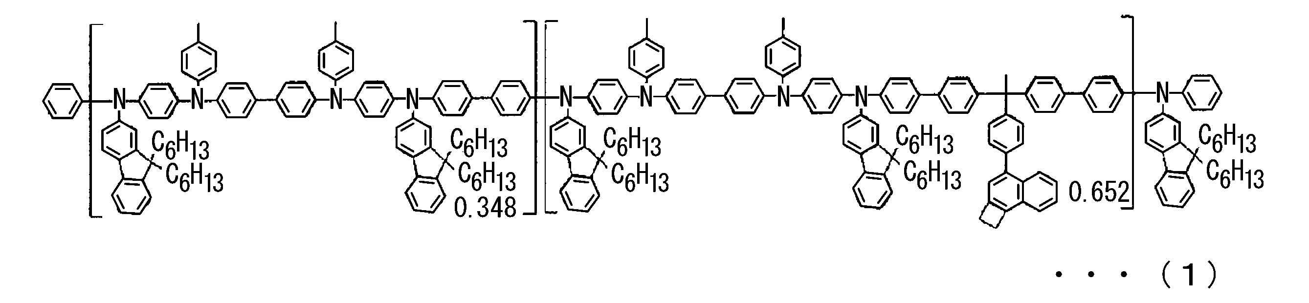
[有機半導体インク組成物の調製]
p型有機半導体は、前述の式(II)で表される化合物(重量平均分子量80000)を用いた。
n型有機半導体は、前述の式(I)において、Aが炭素原子、X1~X4がそれぞれ塩素原子、R1a,R1bがそれぞれ2-エチルヘキシル基、R2が2-エチルヘキシル基、R3が2-エチルヘキシルオキシ基、R4,R5がそれぞれ水素原子である化合物(分子量1339)を用いた。
p型有機半導体は、前述の式(II)で表される化合物(重量平均分子量80000)を用いた。
n型有機半導体は、前述の式(I)において、Aが炭素原子、X1~X4がそれぞれ塩素原子、R1a,R1bがそれぞれ2-エチルヘキシル基、R2が2-エチルヘキシル基、R3が2-エチルヘキシルオキシ基、R4,R5がそれぞれ水素原子である化合物(分子量1339)を用いた。
p型有機半導体0.11g及びn型有機半導体0.03gをo-キシレン9.68mLに溶解させて有機半導体インク組成物を調製した。
得られた有機半導体インク組成物において、n/p比は0.3であり、有機半導体インク組成物の固形分濃度は14mg/mLであった。
得られた有機半導体インク組成物において、n/p比は0.3であり、有機半導体インク組成物の固形分濃度は14mg/mLであった。
[光電変換層の形成]
得られた有機半導体インク組成物を用いて、正孔輸送層上に毎分1000回転でスピンコートした後、120℃で10分間加熱処理(熱アニール処理)し、光電変換層を形成した。
得られた有機半導体インク組成物を用いて、正孔輸送層上に毎分1000回転でスピンコートした後、120℃で10分間加熱処理(熱アニール処理)し、光電変換層を形成した。
[有機光電変換素子の製造]
光電変換層上に、電子輸送材料としてC60フラーレン(フロンティアカーボン社製)を真空中で成膜し、厚さ40nmの電子輸送層を形成した。
さらに、電子輸送層上に、金属電極材料としてアルミニウムを真空中で成膜し、厚さ100nmの電極層を形成して、有機光電変換素子を得た。
光電変換層に含まれるp型有機半導体とn型有機半導体の質量比(n/p比)は、有機半導体インク組成物に含まれるp型有機半導体とn型有機半導体の質量比と同じである。光電変換層のn/p比を表1に示す。
得られた有機光電変換素子について、上記の方法で耐熱性試験を行い、光電変換層の表面粗さRaを測定した。結果を表1に示す。
また、耐熱性試験後の光電変換層(有機光電変換膜)の表面を走査型プローブ顕微鏡で観察した顕微鏡像(以下、単に「有機光電変換膜の表面の顕微鏡像」という)を図2に示す。
<実施例2>
実施例1において、n型有機半導体の使用量を0.07gに変更した以外は、同様にして有機光電変換素子を製造した。
光電変換層のn/p比、及び光電変換層の表面粗さRaを表1に、有機光電変換膜の表面の顕微鏡像を図3に示す。
実施例1において、n型有機半導体の使用量を0.07gに変更した以外は、同様にして有機光電変換素子を製造した。
光電変換層のn/p比、及び光電変換層の表面粗さRaを表1に、有機光電変換膜の表面の顕微鏡像を図3に示す。
<実施例3>
実施例1において、n型有機半導体の使用量を0.10gに変更した以外は、同様にして有機光電変換素子を製造した。
光電変換層のn/p比、及び光電変換層の表面粗さRaを表1に、有機光電変換膜の表面の顕微鏡像を図4に示す。
実施例1において、n型有機半導体の使用量を0.10gに変更した以外は、同様にして有機光電変換素子を製造した。
光電変換層のn/p比、及び光電変換層の表面粗さRaを表1に、有機光電変換膜の表面の顕微鏡像を図4に示す。
<実施例4>
実施例1において、n型有機半導体の使用量を0.13gに変更した以外は、同様にして有機光電変換素子を製造した。
光電変換層のn/p比、及び光電変換層の表面粗さRaを表1に、有機光電変換膜の表面の顕微鏡像を図5に示す。
実施例1において、n型有機半導体の使用量を0.13gに変更した以外は、同様にして有機光電変換素子を製造した。
光電変換層のn/p比、及び光電変換層の表面粗さRaを表1に、有機光電変換膜の表面の顕微鏡像を図5に示す。
<比較例1>
実施例1において、n型有機半導体の使用量を0.22gに変更した以外は、同様にして有機光電変換素子を製造した。
光電変換層のn/p比、及び光電変換層の表面粗さRaを表1に、有機光電変換膜の表面の画像処理した顕微鏡像を図6に示す。
実施例1において、n型有機半導体の使用量を0.22gに変更した以外は、同様にして有機光電変換素子を製造した。
光電変換層のn/p比、及び光電変換層の表面粗さRaを表1に、有機光電変換膜の表面の画像処理した顕微鏡像を図6に示す。

表1に示されるように、実施例1~4では、耐熱性試験後の有機光電変換層の表面粗さRaが0.8~1.2nmであった。これに対して、比較例1では耐熱性試験後の有機光電変換層の表面粗さRaが25.1nmであった。
実施例1~4の有機光電変換膜は、耐熱性試験後の表面粗さRaが小さいことから、イメージセンサの画素間の特性バラツキ、出画不良等の実用上の問題が起こり難いことが期待される。
比較例1は、p型有機半導体に対してn型有機半導体が過剰であるため、両者の相溶性が不十分であり、耐熱性試験過程において過剰なn型有機半導体同士が凝集し結晶化した結果、表面粗さRaが大きくなったと考えられる。
一方、実施例4は、n型有機半導体の過剰量が適度に抑えられたことにより、n型有機半導体同士の凝集及び結晶化が抑制されて表面粗さが改善したと考えられる。
n型有機半導体よりもp型有機半導体の含有量が多い実施例1~3では、表面粗さRaが小さく、高い平滑性が得られた。高分子化合物であるp型有機半導体が、n型有機半導体に比べて結晶化しにくいためと考えられる。
10 有機光電変換素子
11 第1電極
12 正孔輸送層
13 光電変換層(有機光電変換膜)
14 電子輸送層
15 第2電極
20 有機光電膜
11 第1電極
12 正孔輸送層
13 光電変換層(有機光電変換膜)
14 電子輸送層
15 第2電極
20 有機光電膜
Claims (11)
- p型有機半導体及びn型有機半導体を含有する有機光電変換膜であって、
前記n型有機半導体の分子量が500~5000であり、
前記n型有機半導体は、フラーレン骨格を有さないn型有機半導体の含有量100質量部に対して、フラーレン骨格を有するn型有機半導体の含有割合が0~10質量部であり、
200℃の温度条件に50分間保持する耐熱性試験後の表面粗さRaが0.1~10nmである、有機光電変換膜。 - 有機光電変換膜中における、前記p型有機半導体と前記n型有機半導体の合計含有量が90~100質量%である、請求項1に記載の有機光電変換膜。
- 有機光電変換膜中における、前記p型有機半導体の含有量に対する前記n型有機半導体の含有量の質量比を表すn/p比が、0.2~1.8である、請求項1に記載の有機光電変換膜。
- 請求項1~3のいずれか一項に記載の有機光電変換膜を有する、有機光電変換素子。
- 請求項1~3のいずれか一項に記載の有機光電変換膜の製造方法であって、
前記p型有機半導体と、前記n型有機半導体と、溶媒とを含む有機半導体インク組成物の塗布による塗膜の形成、及び
前記塗膜の固化による有機光電変換膜の形成を含む、有機光電変換膜の製造方法。 - 前記溶媒が芳香族炭化水素系溶媒を含む、請求項5の記載の有機光電変換膜の製造方法。
- 前記有機半導体インク組成物が高沸点添加剤を実質的に含まない、請求項5に記載の有機光電変換膜の製造方法。
- p型有機半導体、n型有機半導体、及び溶媒を含有する有機半導体インク組成物であって、
前記n型有機半導体の分子量が500~5000であり、
前記n型有機半導体は、フラーレン骨格を有さないn型有機半導体の含有量100質量部に対して、フラーレン骨格を有するn型有機半導体の含有割合が0~10質量部であり
高沸点添加剤を実質的に含まない、有機半導体インク組成物。 - 有機半導体インク組成物の全固形分中における、前記p型有機半導体と前記n型有機半導体の合計含有量が90~100質量%である、請求項8に記載の有機半導体インク組成物。
- 有機半導体インク組成物中における、前記p型有機半導体の含有量に対する前記n型有機半導体の含有量の質量比を示すn/p比が、0.2~1.8である、請求項8に記載の有機半導体インク組成物。
- 有機半導体インク組成物の塗布による塗膜の形成、及び前記塗膜の固化により形成された膜の、200℃の温度条件に50分間保持する耐熱性試験後の表面粗さRaが0.1~10nmである、請求項8~10のいずれか一項に記載の有機半導体インク組成物。
Priority Applications (1)
| Application Number | Priority Date | Filing Date | Title |
|---|---|---|---|
| JP2024555853A JPWO2024075810A1 (ja) | 2022-10-05 | 2023-10-05 |
Applications Claiming Priority (2)
| Application Number | Priority Date | Filing Date | Title |
|---|---|---|---|
| JP2022-160986 | 2022-10-05 | ||
| JP2022160986 | 2022-10-05 |
Publications (1)
| Publication Number | Publication Date |
|---|---|
| WO2024075810A1 true WO2024075810A1 (ja) | 2024-04-11 |
Family
ID=90608424
Family Applications (1)
| Application Number | Title | Priority Date | Filing Date |
|---|---|---|---|
| PCT/JP2023/036345 Ceased WO2024075810A1 (ja) | 2022-10-05 | 2023-10-05 | 有機光電変換膜、有機光電変換素子、有機光電変換膜の製造方法、及び有機半導体インク組成物 |
Country Status (3)
| Country | Link |
|---|---|
| JP (1) | JPWO2024075810A1 (ja) |
| TW (1) | TW202425763A (ja) |
| WO (1) | WO2024075810A1 (ja) |
Citations (6)
| Publication number | Priority date | Publication date | Assignee | Title |
|---|---|---|---|---|
| KR20100062855A (ko) * | 2008-12-01 | 2010-06-10 | 광주과학기술원 | 플러렌 유도체, 이를 포함하는 유기태양전지, 및 이를 포함하는 유기박막트랜지스터 |
| JP2012142407A (ja) * | 2010-12-28 | 2012-07-26 | Mitsubishi Chemicals Corp | 光電変換素子及びその製造方法、並びにインク |
| WO2013176180A1 (ja) * | 2012-05-23 | 2013-11-28 | 東レ株式会社 | 光起電力素子および光起電力素子の製造方法 |
| WO2019098003A1 (ja) * | 2017-11-17 | 2019-05-23 | ソニーセミコンダクタソリューションズ株式会社 | 光電変換素子および固体撮像装置 |
| WO2020130133A1 (ja) * | 2018-12-20 | 2020-06-25 | 三菱ケミカル株式会社 | 有機フォトダイオード及び赤外線cmosセンサー |
| JP2021057579A (ja) * | 2019-09-30 | 2021-04-08 | 東レ株式会社 | 有機半導体組成物、光起電力素子、光電変換デバイスおよび光起電力素子の製造方法 |
-
2023
- 2023-10-05 WO PCT/JP2023/036345 patent/WO2024075810A1/ja not_active Ceased
- 2023-10-05 TW TW112138220A patent/TW202425763A/zh unknown
- 2023-10-05 JP JP2024555853A patent/JPWO2024075810A1/ja active Pending
Patent Citations (6)
| Publication number | Priority date | Publication date | Assignee | Title |
|---|---|---|---|---|
| KR20100062855A (ko) * | 2008-12-01 | 2010-06-10 | 광주과학기술원 | 플러렌 유도체, 이를 포함하는 유기태양전지, 및 이를 포함하는 유기박막트랜지스터 |
| JP2012142407A (ja) * | 2010-12-28 | 2012-07-26 | Mitsubishi Chemicals Corp | 光電変換素子及びその製造方法、並びにインク |
| WO2013176180A1 (ja) * | 2012-05-23 | 2013-11-28 | 東レ株式会社 | 光起電力素子および光起電力素子の製造方法 |
| WO2019098003A1 (ja) * | 2017-11-17 | 2019-05-23 | ソニーセミコンダクタソリューションズ株式会社 | 光電変換素子および固体撮像装置 |
| WO2020130133A1 (ja) * | 2018-12-20 | 2020-06-25 | 三菱ケミカル株式会社 | 有機フォトダイオード及び赤外線cmosセンサー |
| JP2021057579A (ja) * | 2019-09-30 | 2021-04-08 | 東レ株式会社 | 有機半導体組成物、光起電力素子、光電変換デバイスおよび光起電力素子の製造方法 |
Also Published As
| Publication number | Publication date |
|---|---|
| JPWO2024075810A1 (ja) | 2024-04-11 |
| TW202425763A (zh) | 2024-06-16 |
Similar Documents
| Publication | Publication Date | Title |
|---|---|---|
| Zhou et al. | Glycol monomethyl ether‐substituted carbazolyl hole‐transporting material for stable inverted perovskite solar cells with efficiency of 25.52% | |
| JP5649970B2 (ja) | 有機光電池を製造するための処理添加剤 | |
| Moulé et al. | Two novel cyclopentadithiophene-based alternating copolymers as potential donor components for high-efficiency bulk-heterojunction-type solar cells | |
| Valouch et al. | Solution processed small molecule organic interfacial layers for low dark current polymer photodiodes | |
| JP7400734B2 (ja) | 有機フォトダイオード及び赤外線cmosセンサー | |
| TW201945513A (zh) | 電荷輸送性組成物 | |
| TWI829856B (zh) | 鈣鈦礦光電變換元件用電荷輸送性組成物 | |
| JP2015514327A (ja) | 有機光起電力デバイスのための正孔キャリア層 | |
| JP2021057422A (ja) | Cmosイメージセンサ | |
| JP7339239B2 (ja) | 光電変換素子 | |
| Huang et al. | Triggering the donor–acceptor phase segregation with solid additives enables 16.5% efficiency in all-polymer solar cells | |
| Opoku et al. | Bis‐Diketopyrrolopyrrole and Carbazole‐Based Terpolymer for High Performance Organic Field‐Effect Transistors and Infra‐Red Photodiodes | |
| Zhou et al. | Realizing 8.6% Efficiency from Non‐Halogenated Solvent Processed Additive Free All Polymer Solar Cells with a Quinoxaline Based Polymer | |
| JP2024054634A (ja) | 有機光電変換素子の製造方法及び有機光電変換素子 | |
| CN111819706A (zh) | 光电转换元件 | |
| Xiao et al. | Improved efficiency and stability of inverted polymer solar cells with a solution-processed BPhen interlayer and polystyrene beads | |
| JP5444743B2 (ja) | 有機光電変換素子 | |
| TW201831559A (zh) | 有機光電轉換元件之電洞聚集層用組成物 | |
| Bhardwaj et al. | Surface and grain boundary passivation using tetraphenylethylene derivative for high-performance perovskite solar cell | |
| WO2024075812A1 (ja) | 有機半導体インク組成物の製造方法、有機半導体インク組成物、有機光電変換膜、及び有機光電変換素子 | |
| WO2023157864A1 (ja) | 有機半導体インク、有機膜、光電変換層、光電変換層の製造方法及び有機光電変換素子 | |
| JP7080132B2 (ja) | 光検出素子 | |
| TW202425763A (zh) | 有機光電變換膜、有機光電變換元件、有機光電變換膜之製造方法、及有機半導體墨水組合物 | |
| TWI858246B (zh) | 光檢測元件、感測器、生物體認證裝置、x射線感測器、近紅外線感測器、組成物及油墨組成物 | |
| JP2024116851A (ja) | 有機半導体インク、光電変換層及び有機光電変換素子 |
Legal Events
| Date | Code | Title | Description |
|---|---|---|---|
| 121 | Ep: the epo has been informed by wipo that ep was designated in this application |
Ref document number: 23874935 Country of ref document: EP Kind code of ref document: A1 |
|
| WWE | Wipo information: entry into national phase |
Ref document number: 2024555853 Country of ref document: JP |
|
| NENP | Non-entry into the national phase |
Ref country code: DE |
|
| 122 | Ep: pct application non-entry in european phase |
Ref document number: 23874935 Country of ref document: EP Kind code of ref document: A1 |