WO2024075427A1 - 積層セラミックコンデンサ - Google Patents
積層セラミックコンデンサ Download PDFInfo
- Publication number
- WO2024075427A1 WO2024075427A1 PCT/JP2023/030832 JP2023030832W WO2024075427A1 WO 2024075427 A1 WO2024075427 A1 WO 2024075427A1 JP 2023030832 W JP2023030832 W JP 2023030832W WO 2024075427 A1 WO2024075427 A1 WO 2024075427A1
- Authority
- WO
- WIPO (PCT)
- Prior art keywords
- external electrode
- multilayer ceramic
- ceramic capacitor
- main surface
- plated
- Prior art date
- Legal status (The legal status is an assumption and is not a legal conclusion. Google has not performed a legal analysis and makes no representation as to the accuracy of the status listed.)
- Ceased
Links
Images


Classifications
-
- H—ELECTRICITY
- H01—ELECTRIC ELEMENTS
- H01G—CAPACITORS; CAPACITORS, RECTIFIERS, DETECTORS, SWITCHING DEVICES, LIGHT-SENSITIVE OR TEMPERATURE-SENSITIVE DEVICES OF THE ELECTROLYTIC TYPE
- H01G4/00—Fixed capacitors; Processes of their manufacture
- H01G4/30—Stacked capacitors
-
- H—ELECTRICITY
- H01—ELECTRIC ELEMENTS
- H01G—CAPACITORS; CAPACITORS, RECTIFIERS, DETECTORS, SWITCHING DEVICES, LIGHT-SENSITIVE OR TEMPERATURE-SENSITIVE DEVICES OF THE ELECTROLYTIC TYPE
- H01G4/00—Fixed capacitors; Processes of their manufacture
- H01G4/002—Details
- H01G4/005—Electrodes
-
- H—ELECTRICITY
- H01—ELECTRIC ELEMENTS
- H01G—CAPACITORS; CAPACITORS, RECTIFIERS, DETECTORS, SWITCHING DEVICES, LIGHT-SENSITIVE OR TEMPERATURE-SENSITIVE DEVICES OF THE ELECTROLYTIC TYPE
- H01G4/00—Fixed capacitors; Processes of their manufacture
- H01G4/002—Details
- H01G4/005—Electrodes
- H01G4/012—Form of non-self-supporting electrodes
-
- H—ELECTRICITY
- H01—ELECTRIC ELEMENTS
- H01G—CAPACITORS; CAPACITORS, RECTIFIERS, DETECTORS, SWITCHING DEVICES, LIGHT-SENSITIVE OR TEMPERATURE-SENSITIVE DEVICES OF THE ELECTROLYTIC TYPE
- H01G4/00—Fixed capacitors; Processes of their manufacture
- H01G4/002—Details
- H01G4/018—Dielectrics
- H01G4/06—Solid dielectrics
- H01G4/08—Inorganic dielectrics
- H01G4/12—Ceramic dielectrics
- H01G4/1209—Ceramic dielectrics characterised by the ceramic dielectric material
- H01G4/1218—Ceramic dielectrics characterised by the ceramic dielectric material based on titanium oxides or titanates
- H01G4/1227—Ceramic dielectrics characterised by the ceramic dielectric material based on titanium oxides or titanates based on alkaline earth titanates
-
- H—ELECTRICITY
- H01—ELECTRIC ELEMENTS
- H01G—CAPACITORS; CAPACITORS, RECTIFIERS, DETECTORS, SWITCHING DEVICES, LIGHT-SENSITIVE OR TEMPERATURE-SENSITIVE DEVICES OF THE ELECTROLYTIC TYPE
- H01G4/00—Fixed capacitors; Processes of their manufacture
- H01G4/002—Details
- H01G4/224—Housing; Encapsulation
-
- H—ELECTRICITY
- H01—ELECTRIC ELEMENTS
- H01G—CAPACITORS; CAPACITORS, RECTIFIERS, DETECTORS, SWITCHING DEVICES, LIGHT-SENSITIVE OR TEMPERATURE-SENSITIVE DEVICES OF THE ELECTROLYTIC TYPE
- H01G4/00—Fixed capacitors; Processes of their manufacture
- H01G4/002—Details
- H01G4/228—Terminals
- H01G4/232—Terminals electrically connecting two or more layers of a stacked or rolled capacitor
- H01G4/2325—Terminals electrically connecting two or more layers of a stacked or rolled capacitor characterised by the material of the terminals
-
- H—ELECTRICITY
- H01—ELECTRIC ELEMENTS
- H01G—CAPACITORS; CAPACITORS, RECTIFIERS, DETECTORS, SWITCHING DEVICES, LIGHT-SENSITIVE OR TEMPERATURE-SENSITIVE DEVICES OF THE ELECTROLYTIC TYPE
- H01G4/00—Fixed capacitors; Processes of their manufacture
- H01G4/002—Details
- H01G4/228—Terminals
- H01G4/252—Terminals the terminals being coated on the capacitive element
Definitions
- the present invention relates to a multilayer ceramic capacitor.
- Multilayer ceramic capacitors are widely used in a variety of devices, including electronic devices and electrical devices (hereinafter referred to as "electronic devices, etc.”).
- electronic devices including electronic devices and electrical devices (hereinafter referred to as "electronic devices, etc.”).
- Patent Document 1 JP 2000-100647 A discloses a multilayer ceramic capacitor with a typical structure.
- multilayer ceramic capacitors which are surface-mount electronic components, are often picked up by the nozzle of a mounting device and carried to a designated location on a substrate or the like for mounting. At this time, there is a risk that the impact of the nozzle will cause cracks (including fissures, breaks, chips, etc.) in the ceramic body of the thinned multilayer ceramic capacitor. If cracks occur in the ceramic body, there is a risk that moisture will penetrate from the outside, causing IR (insulation resistance) defects in the multilayer ceramic capacitor.
- multilayer ceramic capacitors are often sealed with resin after being mounted on a substrate or the like.
- the bonding strength between the top surface (second main surface) of the ceramic body of the mounted multilayer ceramic capacitor and the resin can sometimes be insufficient.
- the present invention therefore aims to provide a multilayer ceramic capacitor in which defects such as cracks are unlikely to occur in the ceramic body, even if an impact is applied to the ceramic body by the nozzle of a mounter device, for example, when the ceramic body is picked up by the nozzle.
- the present invention also aims to provide a multilayer ceramic capacitor that has a high bonding strength between the top surface (second main surface) of the ceramic body and the resin when mounted on a substrate or the like and further sealed with resin.
- a multilayer ceramic capacitor includes a ceramic body in which a plurality of ceramic layers, a plurality of first internal electrodes, and a plurality of second internal electrodes are stacked in the height direction, the ceramic body having a first main surface and a second main surface facing in the height direction, a first end surface and a second end surface facing in the length direction perpendicular to the height direction, and a first side surface and a second side surface facing in the width direction perpendicular to the height direction and the length direction, and a first external electrode and a second external electrode formed on the outer surface of the ceramic body, the first internal electrode being drawn out to the first end surface and electrically connected to the first external electrode, and the second internal electrode being drawn out to the second end surface and electrically connected to the second external electrode, the multilayer ceramic capacitor having an L-shape on the first end surface and the first main surface, the second external electrode being L-shaped on the second end surface and the first main surface,
- the multilayer ceramic capacitor according to one embodiment of the present invention has multiple embossed holes formed on the second main surface, so that even if an impact is applied by the nozzle of a mounter device when the capacitor is attached by the nozzle, the capacitor is resistant to the impact and the occurrence of cracks in the ceramic body is suppressed.
- the multilayer ceramic capacitor according to one embodiment of the present invention has a plurality of embossed holes formed in the second main surface, so when the multilayer ceramic capacitor is mounted on a substrate or the like and then sealed with resin, the bonding strength between the second main surface of the ceramic body and the resin is high.
- the multilayer ceramic capacitor of the present invention does not necessarily need to be sealed with resin after being mounted on a substrate or the like, and can also be used without sealing with resin.
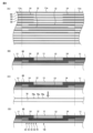
- FIG. 1A and 1B are perspective views of a multilayer ceramic capacitor 100 according to a first embodiment, with FIG. 1A showing the multilayer ceramic capacitor 100 from the first main surface 1A side and FIG. 1B showing the multilayer ceramic capacitor 100 from the second main surface 1B side.
- 1A is a cross-sectional view of the multilayer ceramic capacitor 100, showing a cross section of the portion XX indicated by the dashed dotted line arrow in FIG. 1 is a cross-sectional view of a main portion of a multilayer ceramic capacitor 100.
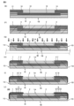
- FIG. 4A to 4D are explanatory views showing steps in an example of a method for manufacturing the multilayer ceramic capacitor 100.
- 5(E) to (J) are continuations of FIG.
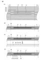
- FIG. 4 is a cross-sectional view of a multilayer ceramic capacitor 200 according to a second embodiment.
- 7A to 7D are explanatory views showing steps in an example of a method for manufacturing the multilayer ceramic capacitor 200.
- 8(E) to (I) are continuations of FIG. 7(D), and are explanatory views showing steps in an example of a method for manufacturing the multilayer ceramic capacitor 200.
- each embodiment is an illustrative example of how the present invention can be implemented, and the present invention is not limited to the contents of the embodiment. It is also possible to combine the contents described in different embodiments, and the implementation in such cases is also included in the present invention.
- the drawings are intended to aid in understanding the specification, and may be drawn diagrammatically, and the dimensional ratios of the depicted components or between the components may not match the dimensional ratios of those components described in the specification. Components described in the specification may be omitted in the drawings, or the number of components may be omitted when drawn.
- Figures 1(A), (B), 2, and 3 each show a multilayer ceramic capacitor 100 according to the first embodiment.
- Figures 1(A) and (B) are each perspective views of the multilayer ceramic capacitor 100, with Figure 1(A) showing the multilayer ceramic capacitor 100 from the first main surface 1A side, and Figure 1(B) showing the multilayer ceramic capacitor 100 from the second main surface 1B side.
- Figure 2 is a cross-sectional view of the multilayer ceramic capacitor 100, showing a cross section of the X-X portion indicated by the dashed dotted line arrow in Figure 1(A).
- Figure 3 is a cross-sectional view of a main portion of the multilayer ceramic capacitor 100.
- the drawings show the height direction T, length direction L, and width direction W of the multilayer ceramic capacitor 100, and these directions may be referred to in the following description.
- the stacking direction of the ceramic layers 1a which will be described later, is the height direction T of the multilayer ceramic capacitor 100.
- the multilayer ceramic capacitor 100 includes a ceramic body 1.
- the ceramic body 1 is a rectangular parallelepiped and has a first main surface 1A and a second main surface 1B that face each other in the height direction T, a first end surface 1C and a second end surface 1D that face each other in the length direction L, and a first side surface 1E and a second side surface 1F that face each other in the width direction W.
- the dimensions of the ceramic body 1 are arbitrary, but for example, it is preferable that one of the dimensions in the length direction L and the width direction W is 1.0 mm or less, and the other is 0.5 mm or less. It is also preferable that the dimension in the height direction T is 0.1 mm or less.
- the ceramic body 1 is composed of a laminate of a ceramic layer 1a, a first internal electrode 2, a second internal electrode 3, and a dummy internal electrode 4.
- the ceramic layer 1a, the first internal electrode 2, the second internal electrode 3, and the dummy internal electrode 4 are laminated in the height direction T of the ceramic body 1.
- the dummy internal electrode 4 is an electrode that is provided not primarily to form capacitance, but as an underlying external electrode for the first external electrode 5 and the second external electrode 6.
- the ceramic body 1 may be made of any material, and may be, for example, a dielectric ceramic containing BaTiO 3 as a main component. However, instead of BaTiO 3 , a dielectric ceramic containing another material as a main component, such as CaTiO 3 , SrTiO 3 , or CaZrO 3 , may be used.
- the thickness of the ceramic layer 1a is arbitrary, but for example, it can be about 0.3 ⁇ m to 2.0 ⁇ m in the effective capacitance formation area where the first internal electrode 2 and the second internal electrode 3 are formed.
- the number of ceramic layers 1a is arbitrary, but for example, in the effective capacitance formation region where the first internal electrode 2 and the second internal electrode 3 are formed, it can be about 1 to 6000 layers.
- a protective layer (outer layer) is provided that does not have the first internal electrode 2 and the second internal electrode 3 and is composed only of the ceramic layer 1a.
- a dummy internal electrode 4 is formed in the protective layer.
- the thickness of the protective layer is arbitrary, but can be, for example, about 5 ⁇ m to 150 ⁇ m.
- the thickness of the ceramic layer 1a of the protective layer may be greater than the thickness of the ceramic layer 1a in the effective region of capacitance formation where the first internal electrode 2 and the second internal electrode 3 are formed.
- the material of the ceramic layer 1a of the protective layer may be different from the material of the ceramic layer 1a in the effective region.
- the first internal electrode 2 extends in the length direction L of the ceramic body 1, with one end extending to a first end face 1C of the ceramic body 1.
- the second internal electrode 3 extends in the length direction L of the ceramic body 1, with one end extending to a second end face 1D of the ceramic body 1.
- the dummy internal electrode 4 provided as an underlying external electrode for the first external electrode 5 and the second external electrode 6 has a smaller dimension in the length direction L than the first internal electrode 2 and the second internal electrode 3.
- One end of the dummy internal electrode 4 is extended to either the first end face 1C or the second end face 1D of the ceramic body 1.
- the dummy internal electrode 4 disposed closest to the first main surface 1A of the ceramic body 1 is exposed to the first main surface 1A of the ceramic body 1.
- At least the dummy internal electrodes 4 are arranged in the first external electrode 5 and the second external electrode 6 closest to the first main surface 1A of the ceramic body 1, and there should be one layer exposed on the first main surface of the ceramic body 1.
- the main components (metal components) of the first internal electrode 2, second internal electrode 3, and dummy internal electrode 4 may be made of any material, but in this embodiment, Ni is used. However, other metals such as Cu, Ag, Pd, and Au may be used instead of Ni. Furthermore, Ni, Cu, Ag, Pd, and Au may be alloyed with other metals.
- the first internal electrode 2, second internal electrode 3, and dummy internal electrode 4 may contain other components such as ceramics in addition to the metal components.
- the thickness of the first internal electrode 2, the second internal electrode 3, and the dummy internal electrode 4 is arbitrary, but can be, for example, about 0.3 ⁇ m to 1.5 ⁇ m.
- a first external electrode 5 and a second external electrode 6 are formed on the outer surface of the ceramic body 1.
- the first external electrode 5 is formed in an L-shape on the first end surface 1C and the first main surface 1A
- the second external electrode 6 is formed in an L-shape on the second end surface 1D and the first main surface 1A.
- the first external electrode 5 is electrically connected to the first internal electrode 2 at the first end surface 1C.
- the second external electrode 6 is electrically connected to the second internal electrode 3 at the second end surface 1D.
- the first external electrode 5 and the second external electrode 6 have the same multi-layer structure.
- the first external electrode 5 and the second external electrode 6 have, in order from the bottom, a base external electrode, a Cu-plated external electrode layer 7 formed on the outside of the base external electrode, a Ni-plated external electrode layer 8 formed on the outside of the Cu-plated external electrode layer 7, and an Au-plated external electrode layer 9 formed on the outside of the Ni-plated external electrode layer 8.
- the structure and materials of the first external electrode 5 and the second external electrode 6 are arbitrary and are not limited to these structures and materials.
- the dimensions such as thickness, width, and length of the first external electrode 5 and the second external electrode 6 are also arbitrary and can be freely set. In particular, various variations can be adopted for the number of layers, materials, dimensions, etc. of the plated external electrode layers.
- the base external electrode is a layer that serves as a base when forming a plated external electrode layer on its outside.
- the base external electrode of the first external electrode 5 is composed of the ends of the first internal electrode 2 and dummy internal electrode 4 drawn out to the first end surface 1C, and the main surface of the dummy internal electrode 4 exposed to the first main surface 1A.
- FIG. 2 illustrates a structure in which the first external electrode 5 has four layers of dummy internal electrodes 4 as base external electrodes, the upper main surface of the dummy internal electrode 4 arranged closest to the first main surface 1A is exposed to the first main surface 1A, and the ends of the remaining three layers of dummy internal electrodes 4 are drawn out to the first end surface 1C.
- the number of layers of the dummy internal electrodes 4 of the first external electrode 5 is arbitrary, and it is sufficient that the first external electrode 5 has at least one layer arranged closest to the first main surface 1A of the ceramic body 1 and whose upper main surface is exposed to the outside from the first main surface 1A of the ceramic body 1.
- the base external electrode of the second external electrode 6 is composed of the ends of the second internal electrode 3 and the dummy internal electrode 4 drawn out to the second end surface 1D, and the main surface of the dummy internal electrode 4 exposed to the first main surface 1A.
- the second external electrode 6 has four layers of dummy internal electrodes 4 as base external electrodes, the upper main surface of the dummy internal electrode 4 arranged closest to the first main surface 1A is exposed to the first main surface 1A, and the ends of the remaining three layers of dummy internal electrodes 4 are drawn out to the second end surface 1D.
- the number of layers of the dummy internal electrodes 4 of the second external electrode 6 is arbitrary, and it is sufficient that the second external electrode 6 has at least one layer arranged closest to the first main surface 1A of the ceramic body 1 and whose upper main surface is exposed to the outside from the first main surface 1A of the ceramic body 1.
- the end of the first internal electrode 2 extended to the first end face 1C of the ceramic body 1 and the end of the second internal electrode 3 extended to the second end face 1D of the ceramic body 1 are also part of the underlying external electrodes of the first external electrode 5 and the second external electrode 6.
- the end of the first internal electrode 2 and the end of the second internal electrode 3 are not shown as part of the first external electrode 5 and the second external electrode 6 to avoid complicating the drawings (the leading lines from the reference numeral "5" indicating the first external electrode 5 and the reference numeral "6" indicating the second external electrode 6 have been omitted).
- the base external electrodes of the first external electrode 5 and the second external electrode 6 function as a base for forming a Cu-plated external electrode layer 7 on the outside thereof.
- the end of the first internal electrode 2 extended to the first end face 1C, the end of the dummy internal electrode 4, the end of the second internal electrode 3 extended to the second end face 1D, and the end of the dummy internal electrode 4 are also part of the base external electrodes of the first external electrode 5 and the second external electrode 6.
- the ends of the multiple linear first internal electrodes 2 and the ends of the dummy internal electrodes 4 extending in the width direction W are exposed, and on the second end face 1D, the ends of the multiple linear second internal electrodes 3 and the ends of the dummy internal electrodes 4 extending in the width direction W are exposed at intervals (with the ends of the linear ceramic layers 1a extending in the width direction W sandwiched between them).
- the ends of the first internal electrodes 2, the ends of the second internal electrodes 3, and the ends of the dummy internal electrodes 4 are spaced apart, they function as a base when forming the plated external electrode layer.
- the first external electrode 5 and the second external electrode 6 each have a Cu-plated external electrode layer 7 on the outside of the base external electrode.
- the Cu-plated external electrode layer 7 mainly functions to improve moisture resistance. It is also preferable that the Cu-plated external electrode layer 7 contains Ni. In this case, dissolution of the external electrode layer into the solder can be suppressed.
- the first external electrode 5 and the second external electrode 6 each have a Ni-plated external electrode layer 8 on the outside of the Cu-plated external electrode layer 7.
- the Ni-plated external electrode layer 8 mainly functions to improve solder heat resistance and bondability. It is also preferable that the Ni-plated external electrode layer 8 contains P. In this case, the mechanical strength of the external electrode layer can be improved.
- the first external electrode 5 and the second external electrode 6 have an Au-plated external electrode layer 9 on the outside of the Ni-plated external electrode layer 8.
- the Au-plated external electrode layer 9 mainly serves the function of improving the wettability of the external electrode layer to the solder.
- the R dimension of the ridge where the first main surface 1A meets the first end surface 1C, the second end surface 1D, the first side surface 1E, and the second side surface 1F is larger than the R dimension of the ridge where the second main surface 1B meets the first end surface 1C, the second end surface 1D, the first side surface 1E, and the second side surface 1F. It is preferable that the R dimension of the ridge where the first main surface 1A meets the first end surface 1C, the second end surface 1D, the first side surface 1E, and the second side surface 1F is, for example, 1 ⁇ m or more and 10 ⁇ m or less. On the other hand, it is preferable that the R dimension of the ridge where the second main surface 1B meets the second end surface 1D, the first side surface 1E, and the second side surface 1F is, for example, less than 1 ⁇ m.
- the first main surface 1A of the ceramic body 1, which is provided with the first external electrode 5 and the second external electrode 6, is the mounting surface to a substrate or the like.
- the R dimension of the ridges where the first main surface 1A, which is the mounting surface, meets the first end surface 1C, the second end surface 1D, the first side surface 1E, and the second side surface 1F is large (largely rounded), so that when the multilayer ceramic capacitor 100 is placed (placed) on a substrate or the like for mounting, even if these ridges or the corners where the first main surface 1A meets two surfaces selected from the first end surface 1C, the second end surface 1D, the first side surface 1E, and the second side surface 1F collide with the substrate or the like, the occurrence of cracks or the like in the ceramic body 1 is suppressed.
- the R dimension of the ridge where the first main surface 1A meets the first end surface 1C, the second end surface 1D, the first side surface 1E, and the second side surface 1F is, for example, about 1 ⁇ m or more and 10 ⁇ m or less. If it is less than 1 ⁇ m, the effect of suppressing the occurrence of cracks in the ceramic body 1 is small. Also, if it exceeds 10 ⁇ m, the effective volume of the ceramic body 1 becomes small, which may hinder the formation of the first internal electrode 2 and the second internal electrode 3, and may reduce the capacitance of the multilayer ceramic capacitor 100.
- the multilayer ceramic capacitor 100 of this embodiment has a plurality of embossed holes 10 formed on the second main surface 1B of the ceramic body 1.
- a plurality of embossed holes 10 of the same shape and dimensions are formed on the second main surface 1B of the ceramic body 1 in a state aligned in the length direction L and width direction W.
- an embossed hole refers to a bottomed hole with a concave surface.
- the concave surface may be hemispherical or non-hemispherical.
- the method of forming the embossed holes 10 is also arbitrary. Whether or not embossed holes 10 are formed in the second main surface 1B can be easily confirmed by comparing with other surfaces of the ceramic body 1 (such as the first main surface 1A).
- the second main surface 1B of the ceramic body 1 is the surface that is sucked by, for example, the nozzle of a mounter device during mounting, and is the surface that may be subjected to impact by the nozzle.
- the multilayer ceramic capacitor 100 of this embodiment since a plurality of embossed holes 10 are formed in the second main surface 1B of the ceramic body 1, even if an impact is applied by a nozzle or the like, the multilayer ceramic capacitor 100 is resistant to the impact, and the occurrence of cracks in the ceramic body 1 is suppressed. Note that if the embossed holes 10 are minute and the depth fits within one to several tens of ceramic layers 1a, the impact resistance of the ceramic body 1 can be improved satisfactorily. However, if the depth of the embossed holes 10 is too large, it may conversely reduce the overall strength of the ceramic body 1, so it is necessary that the depth of the embossed holes 10 is not too large.
- the multilayer ceramic capacitor 100 of this embodiment can be manufactured, for example, by the method shown in Figures 4(A) to 5(J).
- a ceramic green sheet 11a is prepared for producing the ceramic layer 1a of the ceramic body 1, as shown in FIG. 4(A).
- the ceramic green sheet 11a is prepared as a mother ceramic green sheet 50 in which a large number of ceramic green sheets 11a are arranged in a matrix in order to manufacture a large number of multilayer ceramic capacitors 100 at once.
- dielectric ceramic powder, binder resin, solvent, etc. are prepared and then wet-mixed to create ceramic slurry.
- the ceramic slurry is applied in sheet form onto the carrier film using a die coater, gravure coater, microgravure coater, etc., and dried to produce the mother ceramic green sheet 50.
- a conductive paste 12 for forming the first internal electrode 2, a conductive paste 13 for forming the second internal electrode 3, and a conductive paste 14 for forming the dummy internal electrode 4, which have been prepared in advance, are applied (e.g., printed) in a desired pattern shape to the main surface of a predetermined ceramic green sheet 11a in the mother ceramic green sheet 50.
- the conductive paste may be, for example, a mixture of a solvent, a binder resin, a metal powder (e.g., Ni powder), etc.
- the mother ceramic green sheets 50 are stacked in a predetermined order and pressed together to produce a mother unsintered ceramic body 60 in which numerous unsintered ceramic bodies 11 are arranged in a matrix.
- a jig 70 is prepared with multiple protrusions 70a formed on its upper main surface. Then, the lower main surface of the mother unsintered ceramic body 60 is pressed against the protrusions 70a of the jig 70. As a result, as shown in FIG. 4(D), multiple embossed holes 10 are formed in the second main surface 1B of each unsintered ceramic body 11 of the mother unsintered ceramic body 60.
- the mother unsintered ceramic body 60 is cut into individual unsintered ceramic bodies 11.
- the unsintered ceramic body 11 is fired with a predetermined profile to produce the ceramic body 1 shown in FIG. 5(F).
- a conductive paste 12 is fired at the same time to form a first internal electrode 2
- a conductive paste 13 is fired at the same time to form a second internal electrode 3
- a conductive paste 14 is fired at the same time to form a dummy internal electrode 4.
- a jig 80 is prepared.
- the second main surface 1B of the ceramic body 1 is fixed to the upper main surface of the jig 80.
- the first main surface 1A of the ceramic body 1 is scraped off, for example by sandblasting, so that the upper main surface of the dummy internal electrode 4 that is disposed closest to the first main surface 1A of the ceramic body 1 is exposed to the first main surface 1A of the ceramic body 1.
- the ridges where the first main surface 1A meets the first end surface 1C, the second end surface 1D, the first side surface 1E, and the second side surface 1F are cut and rounded, and the R dimension of the ridges where the first main surface 1A meets the first end surface 1C, the second end surface 1D, the first side surface 1E, and the second side surface 1F becomes larger (more rounded) than the R dimension of the ridges where the second main surface 1B meets the first end surface 1C, the second end surface 1D, the first side surface 1E, and the second side surface 1F.
- the ends of the first internal electrode 2, the second internal electrode 3, and the dummy internal electrode 4 extended to the first end face 1C and the second end face 1D, and the upper main surface of the dummy internal electrode 4 exposed to the first main surface 1A are used as base external electrodes, and a specified catalyst is applied to the surfaces of these base external electrodes as necessary, followed by electroless plating to form a Cu-plated external electrode layer 7.
- a specific catalyst is applied to the outside of the Cu-plated external electrode layer 7 as necessary, and then electroless plating is performed to form the Ni-plated external electrode layer 8.
- the first external electrode 5 is formed in an L-shape on the first end face 1C and first main surface 1A of the ceramic body 1
- the second external electrode 6 is formed in an L-shape on the second end face 1D and first main surface 1A of the ceramic body 1, completing the multilayer ceramic capacitor 100 according to the first embodiment.
- FIG. 6 shows a multilayer ceramic capacitor 200 according to the second embodiment. Note that FIG. 6 is a cross-sectional view of the multilayer ceramic capacitor 200.
- the multilayer ceramic capacitor 200 according to the second embodiment is a modified version of the multilayer ceramic capacitor 100 according to the first embodiment described above.
- the R dimension of the ridgeline where the first main surface 1A meets the first end surface 1C, the second end surface 1D, the first side surface 1E, and the second side surface 1F in the ceramic body 1 is larger than the R dimension of the ridgeline where the second main surface 1B meets the first end surface 1C, the second end surface 1D, the first side surface 1E, and the second side surface 1F.
- the multilayer ceramic capacitor 200 changes this, and makes the R dimension of the ridgeline where the first main surface 1A meets the first end surface 1C, the second end surface 1D, the first side surface 1E, and the second side surface 1F the same or nearly the same as the R dimension of the ridgeline where the second main surface 1B meets the first end surface 1C, the second end surface 1D, the first side surface 1E, and the second side surface 1F.
- the R dimension of the ridgeline where the first main surface 1A meets the first end surface 1C, the second end surface 1D, the first side surface 1E, and the second side surface 1F in the ceramic body 1 of the multilayer ceramic capacitor 200 is smaller than the R dimension of the ridgeline where the first main surface 1A meets the first end surface 1C, the second end surface 1D, the first side surface 1E, and the second side surface 1F in the ceramic body 1 of the multilayer ceramic capacitor 100.
- a dummy internal electrode 4 was used as part of the underlying external electrodes for the first external electrode 5 and the second external electrode 6. This has been changed in the multilayer ceramic capacitor 200, and the dummy internal electrode 4 has been omitted.
- a NiCr thin film layer 27 is formed by sputtering as the underlying external electrode for the first external electrode 25 and the second external electrode 26.
- the NiCr thin film layer 27 has high adhesion to the ceramic body 1, and serves as an excellent underlying external electrode for the first external electrode 25 and the second external electrode 26.
- the plated external electrode layers of the first external electrode 5 and the second external electrode 6 were provided in the order of Cu-plated external electrode layer 7, Ni-plated external electrode layer 8, and Au-plated external electrode layer 9 on the outside of the base external electrode.
- the other configurations of the multilayer ceramic capacitor 200 are the same as those of the multilayer ceramic capacitor 100.
- the multilayer ceramic capacitor 200 has multiple embossed holes 10 formed on the second main surface 1B of the ceramic body 1. Therefore, even if an impact is applied to the second main surface 1B of the ceramic body 1 by a nozzle or the like during mounting, the multilayer ceramic capacitor 200 is also shock-resistant, and the occurrence of cracks in the ceramic body 1 is suppressed.
- the multilayer ceramic capacitor 200 of this embodiment can be manufactured, for example, by the method shown in Figures 7(A) to 8(I).
- a ceramic green sheet 11a is prepared for producing the ceramic layer 1a of the ceramic body 1, as shown in FIG. 7(A).
- the ceramic green sheet 11a is prepared as a mother ceramic green sheet 50 for manufacturing a large number of multilayer ceramic capacitors 100 at once.
- a conductive paste 12 for forming the first internal electrode 2 and a conductive paste 13 for forming the second internal electrode 3, which have been prepared in advance, are applied in a desired pattern shape to the main surface of a predetermined ceramic green sheet 11a in the mother ceramic green sheet 50. Note that since the multilayer ceramic capacitor 200 does not have a dummy internal electrode, no conductive paste for forming a dummy internal electrode is applied.
- the mother ceramic green sheets 50 are stacked in a predetermined order and pressed together to produce the mother unsintered ceramic body 60.
- the lower main surface of the mother unsintered ceramic body 60 is pressed against a jig 70 having multiple protrusions 70a formed on its upper main surface, and as shown in FIG. 7(D), multiple embossed holes 10 are formed in the second main surface 1B of each unsintered ceramic body 11.
- the mother unsintered ceramic body 60 is cut into individual unsintered ceramic bodies 11.
- the unsintered ceramic body 11 is fired with a predetermined profile to produce the ceramic body 1 shown in Figure 8 (F).
- a NiCr thin film layer 27 is formed by sputtering as a base external electrode for the first external electrode 25 and the second external electrode 26.
- a specified catalyst is applied to the outside of the NiCr thin film layer 27, which is the base external electrode of the first external electrode 25 and the second external electrode 26, if necessary, and then electroless plating is performed to form the Ni-plated external electrode layer 28.
- a predetermined catalyst is applied to the outside of the Ni-plated external electrode layer 28 if necessary, and then electroless plating is performed to form an Au-plated external electrode layer 29.
- an L-shaped first external electrode 25 is formed on the first end face 1C and first main face 1A of the ceramic body 1
- an L-shaped second external electrode 26 is formed on the second end face 1D and first main face 1A of the ceramic body 1, completing the multilayer ceramic capacitor 200 according to the second embodiment.
- a jig 70 having multiple protrusions 70a formed on its upper main surface is prepared, and the second main surface 1B of the unsintered ceramic body 11 is pressed against the protrusions 70a of the jig 70, and then the unsintered ceramic body 11 is fired to form multiple embossed holes 10 in the second main surface 1B.
- the method of forming the embossed holes 10 in the second main surface 1B of the ceramic body 1 is not limited to this method, and various methods can be adopted.
- the embossed holes refer to concave bottomed holes, and the manufacturing method thereof is not limited.
- the embossed holes (concave bottomed holes) may be hemispherical or non-hemispherical.
- the embossed holes 10 are formed over the entire surface of the second main surface 1B of the ceramic body 1, but the embossed holes 10 may be formed in only a partial area of the second main surface 1B of the ceramic body 1.
- multiple embossed holes 10 of the same shape and dimensions are formed on the second main surface 1B of the ceramic body 1 in a state aligned in the length direction L and width direction W of the ceramic body 1, but the shapes and dimensions of the individual embossed holes 10 may differ, and the multiple embossed holes 10 do not have to be formed in a state aligned.
- the multilayer ceramic capacitor according to one embodiment of the present invention is as described in the "Means for solving the problems" section.
- the R dimension of the ridge where the first main surface meets the first end surface, the second end surface, the first side surface, and the second side surface is larger than the R dimension of the ridge where the second main surface meets the first end surface, the second end surface, the first side surface, and the second side surface.
- the first main surface is a mounting surface for a substrate or the like. In this case, the R dimension of the ridge where the first main surface, which is the mounting surface, meets the first end surface, the second end surface, the first side surface, and the second side surface is large.
- the multilayer ceramic capacitor when the multilayer ceramic capacitor is placed (placed) on a substrate or the like for mounting, even if these ridges or the corners where the first main surface meets two surfaces selected from the first end surface, the second end surface, the first side surface, and the second side surface collide with the substrate or the like, the occurrence of cracks or the like in the ceramic body is suppressed.
- the R dimension of the ridges where the first main surface meets the first end face, second end face, first side face, and second side face is 1 ⁇ m or more and 10 ⁇ m or less. If it is less than 1 ⁇ m, the effect of suppressing the generation of cracks in the ceramic body when these ridges collide with a substrate or the like is small. If it exceeds 10 ⁇ m, the effective volume of the ceramic body becomes small, which may hinder the formation of the first internal electrode and second internal electrode, resulting in a risk of a decrease in the capacitance of the multilayer ceramic capacitor.
- the first external electrode and the second external electrode each include a base external electrode and at least one plated external electrode layer formed on the outside of the base external electrode.
- the plated external electrode layer can be easily formed on the outside of the base external electrode by, for example, electroless plating.
- the base external electrode includes a dummy internal electrode that is smaller in length than the first internal electrode and the second internal electrode and is exposed on the first main surface of the ceramic body. In this case, it is possible to easily form the first external electrode and the second external electrode that have a relatively large area on the first main surface of the ceramic body.
- the dummy internal electrode, the first internal electrode, and the second external electrode are formed from the same material. In this case, there is no need to prepare a separate material to form the dummy internal electrode, which is the base external electrode, improving the productivity of the multilayer ceramic capacitor.
- the dummy internal electrode is mainly composed of Ni.
- the ceramic body, the first internal electrode, the second external electrode, and the dummy internal electrode can be easily produced by so-called simultaneous firing.
- the base external electrode is a thin film.
- the base external electrode can be easily formed, for example, by sputtering.
- the thin film is mainly composed of NiCr. In this case, it has high adhesion to the ceramic body and serves as an excellent base external electrode for the first and second external electrodes.
- the plated external electrode layer includes at least one selected from a Cu-plated external electrode layer, a Ni-plated external electrode layer, and an Au-plated external electrode layer.
- various functions are exerted in each plated external electrode layer, and excellent first and second external electrodes can be formed.
- the plated external electrode layer includes a Ni-plated external electrode layer formed on the outside of the base external electrode, and an Au-plated external electrode layer formed on the outside of the Ni-plated external electrode layer.
- the Ni-plated external electrode layer can mainly function to improve the solder heat resistance and bondability
- the Au-plated external electrode layer 9 can mainly function to improve the wettability of the external electrode layer to the solder.
- the plated external electrode layer includes a Cu-plated external electrode layer formed on the outside of the base external electrode, a Ni-plated external electrode layer formed on the outside of the Cu-plated external electrode layer, and an Au-plated external electrode layer formed on the outside of the Ni-plated external electrode layer.
- the Cu-plated external electrode layer 7 can mainly function to improve moisture resistance
- the Ni-plated external electrode layer can mainly function to improve solder heat resistance and bondability
- the Au-plated external electrode layer 9 can mainly function to improve the wettability of the external electrode layer to solder.
- the Ni-plated external electrode layer contains P. In this case, the mechanical strength of the external electrode layer can be improved.
- the Cu-plated external electrode layer contains Ni. In this case, dissolution of the external electrode layer into the solder can be suppressed.
- one of the lengthwise dimension and widthwise dimension is 1.0 mm or less, and the other is 0.5 mm or less. It is also preferable that the heightwise dimension is 0.1 mm or less. Even when the present invention is applied to a multilayer ceramic capacitor that is thus miniaturized and thinned, the embossed holes formed in the second main surface of the ceramic body improve impact resistance and suppress the occurrence of cracks in the ceramic body.
- Ceramic body 1a Ceramic layer 1A: First main surface 1B: Second main surface 1C: First end surface 1D: Second end surface 1E: First side surface 1F: Second side surface 2: First internal electrode 3: Second internal electrode 4: Dummy internal electrode 5: First external electrode 6: Second external electrode 7: Cu-plated external electrode layer 8, 28: Ni-plated external electrode layer 9, 29: Au-plated external electrode layer 27: NiCr thin film layer (base external electrode) 10: Embossed hole
Landscapes
- Engineering & Computer Science (AREA)
- Power Engineering (AREA)
- Manufacturing & Machinery (AREA)
- Microelectronics & Electronic Packaging (AREA)
- Chemical & Material Sciences (AREA)
- Ceramic Engineering (AREA)
- Inorganic Chemistry (AREA)
- Fixed Capacitors And Capacitor Manufacturing Machines (AREA)
- Ceramic Capacitors (AREA)
Priority Applications (4)
| Application Number | Priority Date | Filing Date | Title |
|---|---|---|---|
| KR1020257009427A KR20250051111A (ko) | 2022-10-04 | 2023-08-27 | 적층 세라믹 콘덴서 |
| JP2024555659A JPWO2024075427A1 (https=) | 2022-10-04 | 2023-08-27 | |
| CN202380068722.8A CN120019457A (zh) | 2022-10-04 | 2023-08-27 | 层叠陶瓷电容器 |
| US18/800,362 US20240404750A1 (en) | 2022-10-04 | 2024-08-12 | Multilayer ceramic capacitor |
Applications Claiming Priority (2)
| Application Number | Priority Date | Filing Date | Title |
|---|---|---|---|
| JP2022160612 | 2022-10-04 | ||
| JP2022-160612 | 2022-10-04 |
Related Child Applications (1)
| Application Number | Title | Priority Date | Filing Date |
|---|---|---|---|
| US18/800,362 Continuation US20240404750A1 (en) | 2022-10-04 | 2024-08-12 | Multilayer ceramic capacitor |
Publications (1)
| Publication Number | Publication Date |
|---|---|
| WO2024075427A1 true WO2024075427A1 (ja) | 2024-04-11 |
Family
ID=90607963
Family Applications (1)
| Application Number | Title | Priority Date | Filing Date |
|---|---|---|---|
| PCT/JP2023/030832 Ceased WO2024075427A1 (ja) | 2022-10-04 | 2023-08-27 | 積層セラミックコンデンサ |
Country Status (5)
| Country | Link |
|---|---|
| US (1) | US20240404750A1 (https=) |
| JP (1) | JPWO2024075427A1 (https=) |
| KR (1) | KR20250051111A (https=) |
| CN (1) | CN120019457A (https=) |
| WO (1) | WO2024075427A1 (https=) |
Citations (12)
| Publication number | Priority date | Publication date | Assignee | Title |
|---|---|---|---|---|
| JPH0270402U (https=) * | 1988-11-17 | 1990-05-29 | ||
| JP2004153098A (ja) * | 2002-10-31 | 2004-05-27 | Nec Tokin Corp | 積層セラミックコンデンサおよびその製造方法 |
| JP2012043841A (ja) * | 2010-08-13 | 2012-03-01 | Murata Mfg Co Ltd | 積層型セラミック電子部品およびその製造方法 |
| JP2012164966A (ja) * | 2011-01-21 | 2012-08-30 | Murata Mfg Co Ltd | セラミック電子部品 |
| JP2016072279A (ja) * | 2014-09-26 | 2016-05-09 | 株式会社村田製作所 | 積層セラミックコンデンサ、これを含む積層セラミックコンデンサ連、および、積層セラミックコンデンサの実装体 |
| CN205248112U (zh) * | 2015-12-04 | 2016-05-18 | 东莞市平尚电子科技有限公司 | 贴片高压电容 |
| JP2019062100A (ja) * | 2017-09-27 | 2019-04-18 | 太陽誘電株式会社 | セラミック電子部品およびその製造方法 |
| JP2020167231A (ja) * | 2019-03-28 | 2020-10-08 | 株式会社村田製作所 | 積層セラミックコンデンサおよび積層セラミックコンデンサの製造方法 |
| JP2021120977A (ja) * | 2020-01-30 | 2021-08-19 | 株式会社村田製作所 | 積層セラミック電子部品及び積層セラミック電子部品の実装構造 |
| JP2022085195A (ja) * | 2020-11-27 | 2022-06-08 | 太陽誘電株式会社 | セラミック電子部品、実装基板およびセラミック電子部品の製造方法 |
| JP2022090195A (ja) * | 2020-12-07 | 2022-06-17 | 太陽誘電株式会社 | セラミック電子部品、実装基板およびセラミック電子部品の製造方法 |
| JP2022142240A (ja) * | 2021-03-16 | 2022-09-30 | 株式会社村田製作所 | 積層セラミックコンデンサ |
Family Cites Families (14)
| Publication number | Priority date | Publication date | Assignee | Title |
|---|---|---|---|---|
| JPS6418722U (https=) * | 1987-07-22 | 1989-01-30 | ||
| JPH04352309A (ja) * | 1991-05-29 | 1992-12-07 | Rohm Co Ltd | 積層セラミックコンデンサにおける端子電極の構造及び端子電極の形成方法 |
| JP3427680B2 (ja) * | 1997-07-15 | 2003-07-22 | 株式会社村田製作所 | 電子部品 |
| JP2000100647A (ja) | 1998-09-24 | 2000-04-07 | Kyocera Corp | 積層セラミックコンデンサおよびその製造方法 |
| US7576968B2 (en) * | 2002-04-15 | 2009-08-18 | Avx Corporation | Plated terminations and method of forming using electrolytic plating |
| JP5526908B2 (ja) * | 2010-03-24 | 2014-06-18 | 株式会社村田製作所 | 積層型電子部品 |
| JP2012160586A (ja) * | 2011-02-01 | 2012-08-23 | Murata Mfg Co Ltd | 積層セラミック電子部品およびその製造方法 |
| KR20130123661A (ko) * | 2012-05-03 | 2013-11-13 | 삼성전기주식회사 | 적층 세라믹 전자부품 및 그 제조 방법 |
| KR101422938B1 (ko) * | 2012-12-04 | 2014-07-23 | 삼성전기주식회사 | 기판 내장용 적층 세라믹 전자부품 및 이의 제조방법, 기판 내장용 적층 세라믹 전자부품을 구비하는 인쇄회로기판 |
| KR102466203B1 (ko) * | 2016-03-22 | 2022-11-11 | 삼성전기주식회사 | 커패시터 및 그 제조방법 |
| JP7017893B2 (ja) * | 2017-09-25 | 2022-02-09 | 太陽誘電株式会社 | 積層セラミックコンデンサ |
| JP7421328B2 (ja) * | 2019-12-24 | 2024-01-24 | 太陽誘電株式会社 | セラミック電子部品 |
| JP7401320B2 (ja) * | 2020-01-24 | 2023-12-19 | 株式会社村田製作所 | 積層セラミック電子部品 |
| JP2023158299A (ja) * | 2022-04-18 | 2023-10-30 | 太陽誘電株式会社 | 積層セラミック電子部品、回路基板及び積層セラミック電子部品の製造方法 |
-
2023
- 2023-08-27 WO PCT/JP2023/030832 patent/WO2024075427A1/ja not_active Ceased
- 2023-08-27 JP JP2024555659A patent/JPWO2024075427A1/ja active Pending
- 2023-08-27 KR KR1020257009427A patent/KR20250051111A/ko active Pending
- 2023-08-27 CN CN202380068722.8A patent/CN120019457A/zh active Pending
-
2024
- 2024-08-12 US US18/800,362 patent/US20240404750A1/en active Pending
Patent Citations (12)
| Publication number | Priority date | Publication date | Assignee | Title |
|---|---|---|---|---|
| JPH0270402U (https=) * | 1988-11-17 | 1990-05-29 | ||
| JP2004153098A (ja) * | 2002-10-31 | 2004-05-27 | Nec Tokin Corp | 積層セラミックコンデンサおよびその製造方法 |
| JP2012043841A (ja) * | 2010-08-13 | 2012-03-01 | Murata Mfg Co Ltd | 積層型セラミック電子部品およびその製造方法 |
| JP2012164966A (ja) * | 2011-01-21 | 2012-08-30 | Murata Mfg Co Ltd | セラミック電子部品 |
| JP2016072279A (ja) * | 2014-09-26 | 2016-05-09 | 株式会社村田製作所 | 積層セラミックコンデンサ、これを含む積層セラミックコンデンサ連、および、積層セラミックコンデンサの実装体 |
| CN205248112U (zh) * | 2015-12-04 | 2016-05-18 | 东莞市平尚电子科技有限公司 | 贴片高压电容 |
| JP2019062100A (ja) * | 2017-09-27 | 2019-04-18 | 太陽誘電株式会社 | セラミック電子部品およびその製造方法 |
| JP2020167231A (ja) * | 2019-03-28 | 2020-10-08 | 株式会社村田製作所 | 積層セラミックコンデンサおよび積層セラミックコンデンサの製造方法 |
| JP2021120977A (ja) * | 2020-01-30 | 2021-08-19 | 株式会社村田製作所 | 積層セラミック電子部品及び積層セラミック電子部品の実装構造 |
| JP2022085195A (ja) * | 2020-11-27 | 2022-06-08 | 太陽誘電株式会社 | セラミック電子部品、実装基板およびセラミック電子部品の製造方法 |
| JP2022090195A (ja) * | 2020-12-07 | 2022-06-17 | 太陽誘電株式会社 | セラミック電子部品、実装基板およびセラミック電子部品の製造方法 |
| JP2022142240A (ja) * | 2021-03-16 | 2022-09-30 | 株式会社村田製作所 | 積層セラミックコンデンサ |
Also Published As
| Publication number | Publication date |
|---|---|
| JPWO2024075427A1 (https=) | 2024-04-11 |
| CN120019457A (zh) | 2025-05-16 |
| US20240404750A1 (en) | 2024-12-05 |
| KR20250051111A (ko) | 2025-04-16 |
Similar Documents
| Publication | Publication Date | Title |
|---|---|---|
| JP7275951B2 (ja) | 積層セラミックコンデンサ | |
| KR101823246B1 (ko) | 적층 세라믹 전자 부품 및 그 실장 기판 | |
| EP2187411B1 (en) | Ceramic electronic component terminals | |
| KR102112107B1 (ko) | 전자부품 및 전자부품의 제조 방법 | |
| KR101659153B1 (ko) | 적층 세라믹 커패시터, 적층 세라믹 커패시터의 제조방법 및 적층 세라믹 커패시터의 실장 기판 | |
| JP7196732B2 (ja) | 積層セラミックコンデンサおよび積層セラミックコンデンサの製造方法 | |
| KR101514559B1 (ko) | 적층 세라믹 커패시터 및 그 실장 기판 | |
| KR20170101117A (ko) | 적층 세라믹 콘덴서 | |
| JP3535998B2 (ja) | 積層セラミック電子部品 | |
| KR20250006803A (ko) | 적층 세라믹 커패시터 | |
| KR20150132972A (ko) | 적층 세라믹 전자부품 및 그 실장 기판 | |
| JP7248363B2 (ja) | 積層セラミックキャパシタ及びその製造方法 | |
| KR101452127B1 (ko) | 적층 세라믹 전자 부품, 그 제조 방법 및 그 실장 기판 | |
| JP4463045B2 (ja) | セラミック電子部品及びコンデンサ | |
| CN111755247B (zh) | 层叠陶瓷电容器以及层叠陶瓷电容器的制造方法 | |
| JP2004296936A (ja) | セラミック電子部品 | |
| JP2004235377A (ja) | セラミック電子部品 | |
| JP2003022929A (ja) | 積層セラミックコンデンサ | |
| JP2023098648A (ja) | 積層型電子部品 | |
| US20240395464A1 (en) | Multilayer ceramic capacitor | |
| JP2023079986A (ja) | セラミック電子部品 | |
| CN110189915A (zh) | 电子组件 | |
| US20240395467A1 (en) | Multilayer ceramic capacitor | |
| WO2024075427A1 (ja) | 積層セラミックコンデンサ | |
| JP7459812B2 (ja) | 積層セラミックコンデンサおよび積層セラミックコンデンサの製造方法 |
Legal Events
| Date | Code | Title | Description |
|---|---|---|---|
| 121 | Ep: the epo has been informed by wipo that ep was designated in this application |
Ref document number: 23874559 Country of ref document: EP Kind code of ref document: A1 |
|
| WWE | Wipo information: entry into national phase |
Ref document number: 2024555659 Country of ref document: JP |
|
| ENP | Entry into the national phase |
Ref document number: 20257009427 Country of ref document: KR Kind code of ref document: A |
|
| WWE | Wipo information: entry into national phase |
Ref document number: 1020257009427 Country of ref document: KR |
|
| WWE | Wipo information: entry into national phase |
Ref document number: 202380068722.8 Country of ref document: CN |
|
| WWP | Wipo information: published in national office |
Ref document number: 1020257009427 Country of ref document: KR |
|
| NENP | Non-entry into the national phase |
Ref country code: DE |
|
| WWP | Wipo information: published in national office |
Ref document number: 202380068722.8 Country of ref document: CN |
|
| 122 | Ep: pct application non-entry in european phase |
Ref document number: 23874559 Country of ref document: EP Kind code of ref document: A1 |