WO2024071420A1 - Composant électronique en céramique, boîtier, carte de circuit imprimé et procédé de fabrication de composant électronique en céramique - Google Patents
Composant électronique en céramique, boîtier, carte de circuit imprimé et procédé de fabrication de composant électronique en céramique Download PDFInfo
- Publication number
- WO2024071420A1 WO2024071420A1 PCT/JP2023/035788 JP2023035788W WO2024071420A1 WO 2024071420 A1 WO2024071420 A1 WO 2024071420A1 JP 2023035788 W JP2023035788 W JP 2023035788W WO 2024071420 A1 WO2024071420 A1 WO 2024071420A1
- Authority
- WO
- WIPO (PCT)
- Prior art keywords
- internal electrode
- layers
- electronic component
- ceramic electronic
- face
- Prior art date
Links
- 239000000919 ceramic Substances 0.000 title claims abstract description 74
- 238000000034 method Methods 0.000 title claims description 56
- 238000004519 manufacturing process Methods 0.000 title claims description 19
- 229910052751 metal Inorganic materials 0.000 claims abstract description 101
- 239000002184 metal Substances 0.000 claims abstract description 101
- 238000002844 melting Methods 0.000 claims abstract description 78
- 230000008018 melting Effects 0.000 claims abstract description 60
- 238000003475 lamination Methods 0.000 claims description 37
- 239000000758 substrate Substances 0.000 claims description 36
- 238000007789 sealing Methods 0.000 claims description 18
- 229910000679 solder Inorganic materials 0.000 claims description 12
- 238000010304 firing Methods 0.000 claims description 11
- 229910052797 bismuth Inorganic materials 0.000 claims description 10
- 229910052718 tin Inorganic materials 0.000 claims description 10
- 229910052733 gallium Inorganic materials 0.000 claims description 8
- 229910052738 indium Inorganic materials 0.000 claims description 8
- 229910052782 aluminium Inorganic materials 0.000 claims description 7
- 229910052725 zinc Inorganic materials 0.000 claims description 7
- 238000004806 packaging method and process Methods 0.000 claims description 5
- 229910052745 lead Inorganic materials 0.000 claims description 2
- 239000003985 ceramic capacitor Substances 0.000 description 133
- 238000007747 plating Methods 0.000 description 46
- 239000010949 copper Substances 0.000 description 33
- PXHVJJICTQNCMI-UHFFFAOYSA-N nickel Substances [Ni] PXHVJJICTQNCMI-UHFFFAOYSA-N 0.000 description 32
- 230000008569 process Effects 0.000 description 29
- 239000011230 binding agent Substances 0.000 description 27
- 238000010586 diagram Methods 0.000 description 22
- 239000011135 tin Substances 0.000 description 21
- 238000009792 diffusion process Methods 0.000 description 17
- 229910010293 ceramic material Inorganic materials 0.000 description 12
- 239000011521 glass Substances 0.000 description 12
- 239000000843 powder Substances 0.000 description 12
- RTAQQCXQSZGOHL-UHFFFAOYSA-N Titanium Chemical compound [Ti] RTAQQCXQSZGOHL-UHFFFAOYSA-N 0.000 description 10
- 239000000654 additive Substances 0.000 description 10
- 229910002113 barium titanate Inorganic materials 0.000 description 10
- 239000000203 mixture Substances 0.000 description 10
- 239000002994 raw material Substances 0.000 description 10
- 239000011734 sodium Substances 0.000 description 10
- 229910052796 boron Inorganic materials 0.000 description 8
- 230000000052 comparative effect Effects 0.000 description 8
- 150000001875 compounds Chemical class 0.000 description 8
- 239000011777 magnesium Substances 0.000 description 8
- 150000002739 metals Chemical class 0.000 description 8
- 229910052700 potassium Inorganic materials 0.000 description 8
- 229910052708 sodium Inorganic materials 0.000 description 8
- YXFVVABEGXRONW-UHFFFAOYSA-N Toluene Chemical compound CC1=CC=CC=C1 YXFVVABEGXRONW-UHFFFAOYSA-N 0.000 description 6
- 230000000996 additive effect Effects 0.000 description 6
- 239000011651 chromium Substances 0.000 description 6
- 229910052749 magnesium Inorganic materials 0.000 description 6
- 239000011572 manganese Substances 0.000 description 6
- 239000002245 particle Substances 0.000 description 6
- 239000002002 slurry Substances 0.000 description 6
- 239000011701 zinc Substances 0.000 description 6
- 238000010438 heat treatment Methods 0.000 description 5
- 229910052759 nickel Inorganic materials 0.000 description 5
- 238000005498 polishing Methods 0.000 description 5
- DJOYTAUERRJRAT-UHFFFAOYSA-N 2-(n-methyl-4-nitroanilino)acetonitrile Chemical compound N#CCN(C)C1=CC=C([N+]([O-])=O)C=C1 DJOYTAUERRJRAT-UHFFFAOYSA-N 0.000 description 4
- 229910052692 Dysprosium Inorganic materials 0.000 description 4
- 229910052691 Erbium Inorganic materials 0.000 description 4
- LFQSCWFLJHTTHZ-UHFFFAOYSA-N Ethanol Chemical compound CCO LFQSCWFLJHTTHZ-UHFFFAOYSA-N 0.000 description 4
- 229910052693 Europium Inorganic materials 0.000 description 4
- 229910052688 Gadolinium Inorganic materials 0.000 description 4
- 229910052689 Holmium Inorganic materials 0.000 description 4
- FYYHWMGAXLPEAU-UHFFFAOYSA-N Magnesium Chemical compound [Mg] FYYHWMGAXLPEAU-UHFFFAOYSA-N 0.000 description 4
- 229910052772 Samarium Inorganic materials 0.000 description 4
- VYPSYNLAJGMNEJ-UHFFFAOYSA-N Silicium dioxide Chemical compound O=[Si]=O VYPSYNLAJGMNEJ-UHFFFAOYSA-N 0.000 description 4
- 229910052771 Terbium Inorganic materials 0.000 description 4
- 229910052775 Thulium Inorganic materials 0.000 description 4
- GWEVSGVZZGPLCZ-UHFFFAOYSA-N Titan oxide Chemical compound O=[Ti]=O GWEVSGVZZGPLCZ-UHFFFAOYSA-N 0.000 description 4
- 239000012298 atmosphere Substances 0.000 description 4
- AYJRCSIUFZENHW-UHFFFAOYSA-L barium carbonate Chemical compound [Ba+2].[O-]C([O-])=O AYJRCSIUFZENHW-UHFFFAOYSA-L 0.000 description 4
- JRPBQTZRNDNNOP-UHFFFAOYSA-N barium titanate Chemical compound [Ba+2].[Ba+2].[O-][Ti]([O-])([O-])[O-] JRPBQTZRNDNNOP-UHFFFAOYSA-N 0.000 description 4
- 229910021523 barium zirconate Inorganic materials 0.000 description 4
- DQBAOWPVHRWLJC-UHFFFAOYSA-N barium(2+);dioxido(oxo)zirconium Chemical compound [Ba+2].[O-][Zr]([O-])=O DQBAOWPVHRWLJC-UHFFFAOYSA-N 0.000 description 4
- 230000005540 biological transmission Effects 0.000 description 4
- 229910052804 chromium Inorganic materials 0.000 description 4
- 238000000576 coating method Methods 0.000 description 4
- 239000003989 dielectric material Substances 0.000 description 4
- 229910052748 manganese Inorganic materials 0.000 description 4
- 229910052750 molybdenum Inorganic materials 0.000 description 4
- 229920002037 poly(vinyl butyral) polymer Polymers 0.000 description 4
- 229920000139 polyethylene terephthalate Polymers 0.000 description 4
- 239000005020 polyethylene terephthalate Substances 0.000 description 4
- 229910052761 rare earth metal Inorganic materials 0.000 description 4
- 238000005245 sintering Methods 0.000 description 4
- -1 tetragonal compound Chemical class 0.000 description 4
- 239000010936 titanium Substances 0.000 description 4
- 229910052727 yttrium Inorganic materials 0.000 description 4
- 229910052802 copper Inorganic materials 0.000 description 3
- 230000032798 delamination Effects 0.000 description 3
- 230000000694 effects Effects 0.000 description 3
- 239000007789 gas Substances 0.000 description 3
- 238000007639 printing Methods 0.000 description 3
- OHVLMTFVQDZYHP-UHFFFAOYSA-N 1-(2,4,6,7-tetrahydrotriazolo[4,5-c]pyridin-5-yl)-2-[4-[2-[[3-(trifluoromethoxy)phenyl]methylamino]pyrimidin-5-yl]piperazin-1-yl]ethanone Chemical compound N1N=NC=2CN(CCC=21)C(CN1CCN(CC1)C=1C=NC(=NC=1)NCC1=CC(=CC=C1)OC(F)(F)F)=O OHVLMTFVQDZYHP-UHFFFAOYSA-N 0.000 description 2
- WZFUQSJFWNHZHM-UHFFFAOYSA-N 2-[4-[2-(2,3-dihydro-1H-inden-2-ylamino)pyrimidin-5-yl]piperazin-1-yl]-1-(2,4,6,7-tetrahydrotriazolo[4,5-c]pyridin-5-yl)ethanone Chemical compound C1C(CC2=CC=CC=C12)NC1=NC=C(C=N1)N1CCN(CC1)CC(=O)N1CC2=C(CC1)NN=N2 WZFUQSJFWNHZHM-UHFFFAOYSA-N 0.000 description 2
- YLZOPXRUQYQQID-UHFFFAOYSA-N 3-(2,4,6,7-tetrahydrotriazolo[4,5-c]pyridin-5-yl)-1-[4-[2-[[3-(trifluoromethoxy)phenyl]methylamino]pyrimidin-5-yl]piperazin-1-yl]propan-1-one Chemical compound N1N=NC=2CN(CCC=21)CCC(=O)N1CCN(CC1)C=1C=NC(=NC=1)NCC1=CC(=CC=C1)OC(F)(F)F YLZOPXRUQYQQID-UHFFFAOYSA-N 0.000 description 2
- ZOXJGFHDIHLPTG-UHFFFAOYSA-N Boron Chemical compound [B] ZOXJGFHDIHLPTG-UHFFFAOYSA-N 0.000 description 2
- VYZAMTAEIAYCRO-UHFFFAOYSA-N Chromium Chemical compound [Cr] VYZAMTAEIAYCRO-UHFFFAOYSA-N 0.000 description 2
- RYGMFSIKBFXOCR-UHFFFAOYSA-N Copper Chemical compound [Cu] RYGMFSIKBFXOCR-UHFFFAOYSA-N 0.000 description 2
- GYHNNYVSQQEPJS-UHFFFAOYSA-N Gallium Chemical compound [Ga] GYHNNYVSQQEPJS-UHFFFAOYSA-N 0.000 description 2
- UFHFLCQGNIYNRP-UHFFFAOYSA-N Hydrogen Chemical compound [H][H] UFHFLCQGNIYNRP-UHFFFAOYSA-N 0.000 description 2
- DGAQECJNVWCQMB-PUAWFVPOSA-M Ilexoside XXIX Chemical compound C[C@@H]1CC[C@@]2(CC[C@@]3(C(=CC[C@H]4[C@]3(CC[C@@H]5[C@@]4(CC[C@@H](C5(C)C)OS(=O)(=O)[O-])C)C)[C@@H]2[C@]1(C)O)C)C(=O)O[C@H]6[C@@H]([C@H]([C@@H]([C@H](O6)CO)O)O)O.[Na+] DGAQECJNVWCQMB-PUAWFVPOSA-M 0.000 description 2
- WHXSMMKQMYFTQS-UHFFFAOYSA-N Lithium Chemical compound [Li] WHXSMMKQMYFTQS-UHFFFAOYSA-N 0.000 description 2
- PWHULOQIROXLJO-UHFFFAOYSA-N Manganese Chemical compound [Mn] PWHULOQIROXLJO-UHFFFAOYSA-N 0.000 description 2
- ZOKXTWBITQBERF-UHFFFAOYSA-N Molybdenum Chemical compound [Mo] ZOKXTWBITQBERF-UHFFFAOYSA-N 0.000 description 2
- ZLMJMSJWJFRBEC-UHFFFAOYSA-N Potassium Chemical compound [K] ZLMJMSJWJFRBEC-UHFFFAOYSA-N 0.000 description 2
- XUIMIQQOPSSXEZ-UHFFFAOYSA-N Silicon Chemical compound [Si] XUIMIQQOPSSXEZ-UHFFFAOYSA-N 0.000 description 2
- 229910002367 SrTiO Inorganic materials 0.000 description 2
- ATJFFYVFTNAWJD-UHFFFAOYSA-N Tin Chemical compound [Sn] ATJFFYVFTNAWJD-UHFFFAOYSA-N 0.000 description 2
- 229910052769 Ytterbium Inorganic materials 0.000 description 2
- FQNGWRSKYZLJDK-UHFFFAOYSA-N [Ca].[Ba] Chemical compound [Ca].[Ba] FQNGWRSKYZLJDK-UHFFFAOYSA-N 0.000 description 2
- 230000002159 abnormal effect Effects 0.000 description 2
- 229910045601 alloy Inorganic materials 0.000 description 2
- 239000000956 alloy Substances 0.000 description 2
- XAGFODPZIPBFFR-UHFFFAOYSA-N aluminium Chemical compound [Al] XAGFODPZIPBFFR-UHFFFAOYSA-N 0.000 description 2
- QVGXLLKOCUKJST-UHFFFAOYSA-N atomic oxygen Chemical compound [O] QVGXLLKOCUKJST-UHFFFAOYSA-N 0.000 description 2
- 229910052788 barium Inorganic materials 0.000 description 2
- DSAJWYNOEDNPEQ-UHFFFAOYSA-N barium atom Chemical compound [Ba] DSAJWYNOEDNPEQ-UHFFFAOYSA-N 0.000 description 2
- 229910052454 barium strontium titanate Inorganic materials 0.000 description 2
- 230000015572 biosynthetic process Effects 0.000 description 2
- JCXGWMGPZLAOME-UHFFFAOYSA-N bismuth atom Chemical compound [Bi] JCXGWMGPZLAOME-UHFFFAOYSA-N 0.000 description 2
- 239000011575 calcium Substances 0.000 description 2
- AOWKSNWVBZGMTJ-UHFFFAOYSA-N calcium titanate Chemical compound [Ca+2].[O-][Ti]([O-])=O AOWKSNWVBZGMTJ-UHFFFAOYSA-N 0.000 description 2
- JXDXDSKXFRTAPA-UHFFFAOYSA-N calcium;barium(2+);oxygen(2-);titanium(4+) Chemical compound [O-2].[Ca+2].[Ti+4].[Ba+2] JXDXDSKXFRTAPA-UHFFFAOYSA-N 0.000 description 2
- 239000011248 coating agent Substances 0.000 description 2
- 229910017052 cobalt Inorganic materials 0.000 description 2
- 239000010941 cobalt Substances 0.000 description 2
- GUTLYIVDDKVIGB-UHFFFAOYSA-N cobalt atom Chemical compound [Co] GUTLYIVDDKVIGB-UHFFFAOYSA-N 0.000 description 2
- 229910052681 coesite Inorganic materials 0.000 description 2
- 229910052906 cristobalite Inorganic materials 0.000 description 2
- 230000006866 deterioration Effects 0.000 description 2
- 238000007598 dipping method Methods 0.000 description 2
- 238000007606 doctor blade method Methods 0.000 description 2
- KBQHZAAAGSGFKK-UHFFFAOYSA-N dysprosium atom Chemical compound [Dy] KBQHZAAAGSGFKK-UHFFFAOYSA-N 0.000 description 2
- UYAHIZSMUZPPFV-UHFFFAOYSA-N erbium Chemical compound [Er] UYAHIZSMUZPPFV-UHFFFAOYSA-N 0.000 description 2
- OGPBJKLSAFTDLK-UHFFFAOYSA-N europium atom Chemical compound [Eu] OGPBJKLSAFTDLK-UHFFFAOYSA-N 0.000 description 2
- UIWYJDYFSGRHKR-UHFFFAOYSA-N gadolinium atom Chemical compound [Gd] UIWYJDYFSGRHKR-UHFFFAOYSA-N 0.000 description 2
- 230000012447 hatching Effects 0.000 description 2
- KJZYNXUDTRRSPN-UHFFFAOYSA-N holmium atom Chemical compound [Ho] KJZYNXUDTRRSPN-UHFFFAOYSA-N 0.000 description 2
- 239000001257 hydrogen Substances 0.000 description 2
- 229910052739 hydrogen Inorganic materials 0.000 description 2
- 238000001027 hydrothermal synthesis Methods 0.000 description 2
- APFVFJFRJDLVQX-UHFFFAOYSA-N indium atom Chemical compound [In] APFVFJFRJDLVQX-UHFFFAOYSA-N 0.000 description 2
- 238000009413 insulation Methods 0.000 description 2
- 238000010030 laminating Methods 0.000 description 2
- 229910052744 lithium Inorganic materials 0.000 description 2
- 239000000463 material Substances 0.000 description 2
- 239000011733 molybdenum Substances 0.000 description 2
- 239000012299 nitrogen atmosphere Substances 0.000 description 2
- 239000003960 organic solvent Substances 0.000 description 2
- 238000007254 oxidation reaction Methods 0.000 description 2
- 239000001301 oxygen Substances 0.000 description 2
- 229910052760 oxygen Inorganic materials 0.000 description 2
- 230000000149 penetrating effect Effects 0.000 description 2
- 239000012071 phase Substances 0.000 description 2
- 239000004014 plasticizer Substances 0.000 description 2
- 239000011591 potassium Substances 0.000 description 2
- 238000005036 potential barrier Methods 0.000 description 2
- 238000002360 preparation method Methods 0.000 description 2
- 238000010405 reoxidation reaction Methods 0.000 description 2
- 229920005989 resin Polymers 0.000 description 2
- 239000011347 resin Substances 0.000 description 2
- KZUNJOHGWZRPMI-UHFFFAOYSA-N samarium atom Chemical compound [Sm] KZUNJOHGWZRPMI-UHFFFAOYSA-N 0.000 description 2
- 229910052710 silicon Inorganic materials 0.000 description 2
- 239000010703 silicon Substances 0.000 description 2
- 239000000377 silicon dioxide Substances 0.000 description 2
- 235000012239 silicon dioxide Nutrition 0.000 description 2
- 238000003980 solgel method Methods 0.000 description 2
- 238000010532 solid phase synthesis reaction Methods 0.000 description 2
- 238000004544 sputter deposition Methods 0.000 description 2
- 229910052682 stishovite Inorganic materials 0.000 description 2
- VEALVRVVWBQVSL-UHFFFAOYSA-N strontium titanate Chemical compound [Sr+2].[O-][Ti]([O-])=O VEALVRVVWBQVSL-UHFFFAOYSA-N 0.000 description 2
- 230000002194 synthesizing effect Effects 0.000 description 2
- JBQYATWDVHIOAR-UHFFFAOYSA-N tellanylidenegermanium Chemical compound [Te]=[Ge] JBQYATWDVHIOAR-UHFFFAOYSA-N 0.000 description 2
- GZCRRIHWUXGPOV-UHFFFAOYSA-N terbium atom Chemical compound [Tb] GZCRRIHWUXGPOV-UHFFFAOYSA-N 0.000 description 2
- FRNOGLGSGLTDKL-UHFFFAOYSA-N thulium atom Chemical compound [Tm] FRNOGLGSGLTDKL-UHFFFAOYSA-N 0.000 description 2
- 229910052719 titanium Inorganic materials 0.000 description 2
- 239000004408 titanium dioxide Substances 0.000 description 2
- 230000007723 transport mechanism Effects 0.000 description 2
- 229910052905 tridymite Inorganic materials 0.000 description 2
- 229910052720 vanadium Inorganic materials 0.000 description 2
- LEONUFNNVUYDNQ-UHFFFAOYSA-N vanadium atom Chemical compound [V] LEONUFNNVUYDNQ-UHFFFAOYSA-N 0.000 description 2
- 238000007740 vapor deposition Methods 0.000 description 2
- NAWDYIZEMPQZHO-UHFFFAOYSA-N ytterbium Chemical compound [Yb] NAWDYIZEMPQZHO-UHFFFAOYSA-N 0.000 description 2
- VWQVUPCCIRVNHF-UHFFFAOYSA-N yttrium atom Chemical compound [Y] VWQVUPCCIRVNHF-UHFFFAOYSA-N 0.000 description 2
- 230000008859 change Effects 0.000 description 1
- 238000000354 decomposition reaction Methods 0.000 description 1
- 230000007246 mechanism Effects 0.000 description 1
- 239000000155 melt Substances 0.000 description 1
- 230000004048 modification Effects 0.000 description 1
- 238000012986 modification Methods 0.000 description 1
- 230000001681 protective effect Effects 0.000 description 1
Images


Classifications
-
- H—ELECTRICITY
- H01—ELECTRIC ELEMENTS
- H01G—CAPACITORS; CAPACITORS, RECTIFIERS, DETECTORS, SWITCHING DEVICES, LIGHT-SENSITIVE OR TEMPERATURE-SENSITIVE DEVICES OF THE ELECTROLYTIC TYPE
- H01G13/00—Apparatus specially adapted for manufacturing capacitors; Processes specially adapted for manufacturing capacitors not provided for in groups H01G4/00 - H01G11/00
-
- H—ELECTRICITY
- H01—ELECTRIC ELEMENTS
- H01G—CAPACITORS; CAPACITORS, RECTIFIERS, DETECTORS, SWITCHING DEVICES, LIGHT-SENSITIVE OR TEMPERATURE-SENSITIVE DEVICES OF THE ELECTROLYTIC TYPE
- H01G2/00—Details of capacitors not covered by a single one of groups H01G4/00-H01G11/00
- H01G2/02—Mountings
- H01G2/06—Mountings specially adapted for mounting on a printed-circuit support
-
- H—ELECTRICITY
- H01—ELECTRIC ELEMENTS
- H01G—CAPACITORS; CAPACITORS, RECTIFIERS, DETECTORS, SWITCHING DEVICES, LIGHT-SENSITIVE OR TEMPERATURE-SENSITIVE DEVICES OF THE ELECTROLYTIC TYPE
- H01G4/00—Fixed capacitors; Processes of their manufacture
- H01G4/30—Stacked capacitors
-
- H—ELECTRICITY
- H05—ELECTRIC TECHNIQUES NOT OTHERWISE PROVIDED FOR
- H05K—PRINTED CIRCUITS; CASINGS OR CONSTRUCTIONAL DETAILS OF ELECTRIC APPARATUS; MANUFACTURE OF ASSEMBLAGES OF ELECTRICAL COMPONENTS
- H05K13/00—Apparatus or processes specially adapted for manufacturing or adjusting assemblages of electric components
- H05K13/02—Feeding of components
Definitions
- the present invention relates to ceramic electronic components, packaging bodies, circuit boards, and methods for manufacturing ceramic electronic components.
- known means for suppressing the diffusion of Cu include adjusting the components of the glass added to the conductive paste that forms the external electrode (see, for example, Patent Document 1) or adding a low-melting point metal such as Sn (see, for example, Patent Document 2) to lower the baking temperature.
- the present invention has been made in consideration of the above problems, and aims to provide a ceramic electronic component, a package, a circuit board, and a method for manufacturing a ceramic electronic component that can suppress the occurrence of cracks.
- the ceramic electronic component according to the present invention comprises a laminated chip having a generally rectangular parallelepiped shape in which a number of dielectric layers and a number of internal electrode layers mainly composed of Ni are alternately stacked, and the plurality of internal electrode layers are alternately exposed on a first end face and a second end face that face each other in the generally rectangular parallelepiped shape; and a pair of external electrodes provided on the first end face and the second end face, the main component of the contact layer in contact with the first end face and the second end face being Cu.
- a low-melting point metal having a melting point lower than Cu is added to the plurality of internal electrode layers and the contact layer, and the width of the connection portion connected to the external electrode in at least one of the outermost internal electrode layers among the plurality of internal electrode layers is narrower than the width of other regions.
- the low melting point metal may contain at least one of Ga, In, Sn, Bi, Zn, and Al.
- the number of layers of the internal electrode layer that is one or more from the outermost layer may be 10% or more in total relative to the total number of layers of the multiple internal electrode layers.
- the width of the connection portion may be 1/2 or more and 4/5 or less of the width of the internal electrode layers in the region where the internal electrode layers connected to different external electrodes face each other.
- the length of the connection portion in the direction in which the first end face and the second end face face each other may be at least 1/3 of the distance that the pair of external electrodes extend from the first end face or the second end face to at least one of the four faces of the laminated chip other than the first end face and the second end face.
- the dimension in the first direction may be 1.3 times or more larger than the dimension in the second direction.
- the dimension in the first direction may be 1.3 times or more larger than the dimension in the second direction.
- the thickness of each of the multiple internal electrode layers may be 0.1 ⁇ m or more and 2 ⁇ m or less.
- the thickness of each of the plurality of dielectric layers may be 0.3 ⁇ m or more and 10 ⁇ m or less.
- the packaging body according to the present invention is characterized by comprising any one of the ceramic electronic components described above, a carrier tape having a sealing surface perpendicular to the first direction of a first direction and a second direction perpendicular to the direction in which the first end face and the second end face face each other and perpendicular to each other, and a recess recessed from the sealing surface in the first direction and accommodating the ceramic electronic component, and a top tape attached to the sealing surface and covering the recess.
- the circuit board according to the present invention is characterized by comprising any one of the ceramic electronic components described above, a mounting substrate having a mounting surface perpendicular to the first direction of a first direction and a second direction perpendicular to the direction in which the first end face and the second end face face each other, and a pair of connection electrodes provided on the mounting surface to which the pair of external electrodes of the ceramic electronic component are respectively connected via solder.
- the method for manufacturing a ceramic electronic component according to the present invention includes the steps of firing a laminate in which multiple lamination units, each of which has an internal electrode pattern formed on a dielectric green sheet and which is mainly composed of Ni with an added low-melting point metal having a melting point lower than that of Cu, are laminated, and forming a layer containing the low-melting point metal mainly composed of Cu on a first end face and a second end face facing each other of the laminate during or after firing the laminate, and is characterized in that in at least one internal electrode pattern from the outermost layer among the multiple internal electrode patterns, the width of the connection portion connected to the layer containing the low-melting point metal is narrower than the width of other regions.
- the ceramic electronic component according to the present invention comprises a laminated chip having a dimension in a first direction that is 1.3 times or more the dimension in a second direction perpendicular to the first direction, a plurality of dielectric layers and a plurality of internal electrode layers mainly composed of Ni alternately laminated in the second direction, and having a substantially rectangular shape, the plurality of internal electrode layers alternately exposed on a first end face and a second end face that face a third direction perpendicular to the first direction and the second direction, and a pair of external electrodes provided on the first end face and the second end face, the main component of which is Cu at the portions in contact with the first end face and the second end face, and a low-melting point metal with a melting point lower than Cu is provided inside the plurality of internal electrode layers and at least one of the interfaces between the plurality of internal electrode layers and the plurality of dielectric layers.
- the low melting point metal may contain any one of Ga, In, Sn, Bi, Pb, and Zn.
- the width in the first direction of the connection portion connected to the external electrode may be narrower than the width of other regions.
- the number of layers of the internal electrode layer that is one or more from the outermost layer may be 10% or more and 50% or less of the total number of layers of the multiple internal electrode layers.
- the width of the connection portion in the first direction may be 1/2 or more and 4/5 or less of the width of the internal electrode layer in the first direction in a region where the internal electrode layers connected to different external electrodes face each other.
- the thickness of each of the multiple internal electrode layers may be 0.1 ⁇ m or more and 2 ⁇ m or less.
- the thickness of each of the plurality of dielectric layers may be 0.3 ⁇ m or more and 3 ⁇ m or less.
- the package according to the present invention is characterized by comprising any one of the ceramic electronic components described above, a carrier tape having a sealing surface perpendicular to the first direction and a recess recessed from the sealing surface in the first direction for accommodating the ceramic electronic component, and a top tape attached to the sealing surface and covering the recess.
- the circuit board according to the present invention is characterized by comprising any one of the ceramic electronic components described above, and a mounting substrate having a mounting surface perpendicular to the first direction, and a pair of connection electrodes provided on the mounting surface to which the pair of external electrodes of the ceramic electronic component are respectively connected via solder.
- the method for manufacturing a ceramic electronic component according to the present invention is a method for manufacturing a ceramic electronic component whose dimension in a first direction is 1.3 times or more its dimension in a second direction perpendicular to the first direction, and is characterized by comprising the steps of: firing a laminate in which a plurality of lamination units, each lamination unit having an internal electrode pattern formed on a dielectric green sheet and made of Ni as the main component and a low-melting point metal with a melting point lower than that of Cu, are laminated in the second direction; and forming a layer made of Cu as the main component on a first end face and a second end face of the laminate facing each other in a third direction perpendicular to the first direction and the second direction, during or after firing the laminate.
- the present invention provides ceramic electronic components, packaging bodies, circuit boards, and methods for manufacturing ceramic electronic components that can suppress the occurrence of cracks.
- FIG. 1A and 1B are partial cross-sectional perspective views of the multilayer ceramic capacitor in accordance with the first embodiment.
- 2 is a cross-sectional view taken along line AA in FIG. 1(a) is a cross-sectional view taken along line BB of FIG.
- FIG. 4 is an enlarged cross-sectional view of the vicinity of an external electrode.
- FIG. FIG. 2 is a diagram illustrating a first region and a second region.
- FIG. 13 is a diagram illustrating the dimension e. 1A to 1C are diagrams illustrating a flow of a method for manufacturing a multilayer ceramic capacitor.
- FIG. 2 is a side view of a circuit board including a multilayer ceramic capacitor.
- FIG. 5A and 5B are diagrams illustrating a multilayer ceramic capacitor according to a second embodiment.
- 11A and 11B are diagrams illustrating a multilayer ceramic capacitor according to a third embodiment.
- FIG. 1 is a diagram illustrating a lamination process.
- 13A and 13B are diagrams illustrating a multilayer ceramic capacitor according to a fourth embodiment.
- 13A and 13B are diagrams illustrating a multilayer ceramic capacitor according to a fifth embodiment.
- FIG. 13 is a partial cross-sectional perspective view of a multilayer ceramic capacitor in accordance with a sixth embodiment. This is a cross-sectional view of line AA in Figure 17. This is a cross-sectional view of line BB in Figure 17.
- FIG. 4 is an enlarged cross-sectional view of the vicinity of an external electrode.
- FIG. 1 is a diagram illustrating a lamination process.
- 13A and 13B are diagrams illustrating a multilayer ceramic capacitor according to a fourth embodiment.
- 13A and 13B are diagrams
- FIG. 1 is a diagram illustrating a multilayer ceramic capacitor having a large number of layers.
- FIG. 13 is a diagram illustrating a debinder crack.
- 1A to 1C are diagrams illustrating a flow of a method for manufacturing a multilayer ceramic capacitor.
- FIG. 1 is a diagram illustrating a lamination process.
- FIG. 2 is a side view of a circuit board including a multilayer ceramic capacitor.
- FIG. 27 is a cross-sectional view of the package taken along line DD in FIG. 26.
- 11 is a diagram illustrating a crack at a corner portion near an external electrode.
- FIG. 13A to 13C are diagrams illustrating a multilayer ceramic capacitor according to a seventh embodiment.
- FIG. 13 is a diagram illustrating the dimension e.
- FIG. 1 is a diagram illustrating a lamination process.
- 13A to 13C are diagrams illustrating a multilayer ceramic capacitor according to an eighth embodiment.
- FIG. 1 is a diagram illustrating a
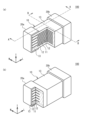
- First Embodiment 1(a) and 1(b) are partial cross-sectional perspective views of the multilayer ceramic capacitor 100 according to the first embodiment.
- FIG. 2 is a cross-sectional view taken along line A-A in FIG. 1(a).
- FIG. 3 is a cross-sectional view taken along line B-B in FIG. 1(a).
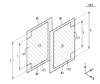
- the multilayer ceramic capacitor 100 includes a laminated chip 10 having a substantially rectangular parallelepiped shape, and external electrodes 20a and 20b provided on two opposing end faces of the laminated chip 10. Of the four faces of the laminated chip 10 other than the two end faces, the two faces at both ends in the lamination direction are referred to as the upper face and the lower face.
- the two faces other than the two end faces, the upper face, and the lower face are referred to as the side faces.
- the external electrodes 20a and 20b extend to the upper face, the lower face, and the two side faces in the lamination direction of the laminated chip 10. However, the external electrodes 20a and the external electrodes 20b are spaced apart from each other.
- the T direction (first direction) is the height direction of the multilayer ceramic capacitor 100, and is perpendicular to the direction in which the external electrodes 20a and 20b face each other (length direction: L direction).
- the W direction (second direction) is perpendicular to the T direction and the L direction.
- the T direction corresponds to the stacking direction of the internal electrode layers 12, and is the direction in which the upper and lower surfaces of the multilayer chip 10 face each other.
- the W direction is the direction in which the two side surfaces of the multilayer chip 10 face each other.
- the L direction is the direction in which the two end faces of the multilayer chip 10 face each other.
- the multilayer ceramic capacitor 100 in the T direction is defined as height T0
- the width of the multilayer ceramic capacitor 100 in the W direction is defined as width W0
- the length of the multilayer ceramic capacitor 100 in the L direction is defined as length L0
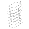
- the laminated chip 10 has a configuration in which dielectric layers 11 containing a ceramic material that functions as a dielectric and internal electrode layers 12 mainly composed of metal are alternately laminated.
- the laminated chip 10 has a plurality of internal electrode layers 12 facing each other and a dielectric layer 11 sandwiched between the plurality of internal electrode layers 12.
- the edges in the direction in which each internal electrode layer 12 extends are alternately exposed to the first end face on which the external electrode 20a of the laminated chip 10 is provided and the second end face on which the external electrode 20b is provided.
- the internal electrode layer 12 connected to the external electrode 20a is not connected to the external electrode 20b.
- the internal electrode layer 12 connected to the external electrode 20b is not connected to the external electrode 20a.
- each internal electrode layer 12 is alternately conductive to the external electrode 20a and the external electrode 20b.
- the internal electrode layer 12 is disposed on the top layer in the lamination direction, and the internal electrode layer 12 is also disposed on the bottom layer in the lamination direction, and both end faces in the lamination direction of the laminate are covered with a cover layer 13.
- the cover layer 13 is mainly composed of a ceramic material.
- the main component of the cover layer 13 is the same as the main component of the dielectric layer 11.
- the dielectric layer 11 has a main phase of a ceramic material having a perovskite structure represented by the general formula ABO 3.
- the perovskite structure includes ABO 3- ⁇ , which is not a stoichiometric composition.
- the ceramic material can be selected from at least one of BaTiO 3 (barium titanate), CaZrO 3 (calcium zirconate), CaTiO 3 (calcium titanate), SrTiO 3 (strontium titanate), MgTiO 3 (magnesium titanate), Ba 1-x-y Ca x Sr y Ti 1-z Zr z O 3 (0 ⁇ x ⁇ 1, 0 ⁇ y ⁇ 1, 0 ⁇ z ⁇ 1) that forms a perovskite structure, and the like.
- Ba1 -xyCaxSryTi1 - zZrzO3 is barium strontium titanate, barium calcium titanate, barium zirconate, barium zirconate titanate, calcium zirconate titanate and barium calcium zirconate titanate, etc.
- the dielectric layer 11 may contain additives.
- additives to the dielectric layer 11 include oxides of magnesium (Mg), manganese (Mn), molybdenum (Mo), vanadium (V), chromium (Cr), rare earth elements (yttrium (Y), samarium (Sm), europium (Eu), gadolinium (Gd), terbium (Tb), dysprosium (Dy), holmium (Ho), erbium (Er), thulium (Tm), and ytterbium (Yb)), or oxides containing cobalt (Co), nickel (Ni), lithium (Li), boron (B), sodium (Na), potassium (K), or silicon (Si), or glasses containing Co, Ni, Li, B, Na, K, or Si.
- each dielectric layer 11 in the stacking direction is, for example, 0.3 ⁇ m to 10 ⁇ m, or 0.4 ⁇ m to 8 ⁇ m, or 0.5 ⁇ m to 5 ⁇ m.
- the thickness of each dielectric layer 11 can be measured by exposing the cross section of the multilayer ceramic capacitor 100, for example, as shown in FIG. 2, by mechanical polishing, and then obtaining the average thickness value at 10 points from an image taken by a microscope such as a scanning transmission electron microscope.
- the internal electrode layer 12 is mainly composed of Ni.
- the thickness of each internal electrode layer 12 in the lamination direction is, for example, 0.1 ⁇ m or more and 2 ⁇ m or less.
- the thickness of each internal electrode layer 12 can be measured by exposing the cross section of the multilayer ceramic capacitor 100, for example, as shown in FIG. 2, by mechanical polishing, and then obtaining the average thickness value at 10 points from an image taken by a microscope such as a scanning transmission electron microscope.
- the region where the internal electrode layer 12 connected to the external electrode 20a and the internal electrode layer 12 connected to the external electrode 20b face each other is a region that generates capacitance in the multilayer ceramic capacitor 100. Therefore, this region that generates capacitance is referred to as the capacitance section 14.
- the capacitance section 14 is a region where adjacent internal electrode layers connected to different external electrodes face each other.
- the region where the internal electrode layers 12 connected to the external electrode 20a face each other without an internal electrode layer 12 connected to the external electrode 20b being interposed therebetween is called the end margin 15.
- the region where the internal electrode layers 12 connected to the external electrode 20b face each other without an internal electrode layer 12 connected to the external electrode 20a being interposed therebetween is also the end margin 15.
- the end margin is the region where the internal electrode layers connected to the same external electrode face each other without an internal electrode layer connected to a different external electrode being interposed therebetween.
- the end margin 15 is a region that does not generate capacitance.
- the end margin 15 may have the same composition as the dielectric layer 11 of the capacitance section 14, or may have a different composition.
- the areas extending from the two side surfaces to the internal electrode layer 12 are called side margins 16.
- the side margins 16 are also areas that do not generate capacitance.
- the side margins 16 may have the same composition as the dielectric layer 11 of the capacitance section 14, or may have a different composition.
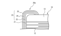
- the external electrode 20a has a structure in which a plating layer 22 is provided on a base layer 21, which is a contact layer in contact with the first end face of the laminated chip 10.
- the base layer 21 is mainly composed of Cu.
- the base layer 21 may also contain a glass component.
- the plating layer 22 is mainly composed of a metal such as Cu, Ni, aluminum (Al), zinc (Zn), Sn, etc., or an alloy of two or more of these.
- the plating layer 22 may be a plating layer of a single metal component, or may be a plurality of plating layers of different metal components.
- the plating layer 22 has a structure in which a first plating layer 23, a second plating layer 24, and a third plating layer 25 are formed in this order from the base layer 21 side.
- the first plating layer 23 is, for example, a Sn plating layer.
- the second plating layer 24 is, for example, a Ni plating layer.
- the third plating layer 25 is, for example, a Sn plating layer.
- the external electrode 20a is illustrated, but the external electrode 20b also has a similar laminated structure.
- the multilayer ceramic capacitor 100 according to this embodiment has a configuration that can suppress the occurrence of cracks due to Cu diffusion without excessively lowering the baking temperature.
- the internal electrode layer 12 and the underlayer 21 contain a low-melting-point metal that has a lower melting point than Cu, which is the main metal component of the underlayer 21.
- the low-melting-point metal is not particularly limited as long as it has a lower melting point than Cu, but examples of the low-melting-point metal include Ga (gallium), In (indium), Sn, Bi (bismuth), Zn, and Al.
- the low melting point metal may be alloyed with Ni, which is the main component of the internal electrode layer 12, or may be disposed as a single metal.
- the low melting point metal may be disposed in a uniformly dispersed manner in the internal electrode layer 12, or may be segregated at the interface between the internal electrode layer 12 and the dielectric layer 11.
- the low melting point metal may be alloyed with Cu, which is the main component of the underlayer 21, or may be disposed as a single metal.
- the low melting point metal may be disposed in a uniformly dispersed manner in the underlayer 21, or may be segregated at the interface between the underlayer 21 and the laminated chip 10.
- each internal electrode layer 12 in the in-plane direction has a first region 121 (connection portion) connected to the external electrode 20a in a region corresponding to the end margin 15 and having a dimension W1 in the W direction, and a second region 122 in a region corresponding to the capacitance portion 14 and having a dimension W2 in the W direction.
- the dimension W1 is smaller than the dimension W2.
- the first region 121 is located inside the second region 122.
- the internal electrode layer 12 connected to the external electrode 20b also has a first region 121 having a dimension W1 and a second region 122 having a dimension W2.
- the center of the first region 121 in the W direction coincides with the center of the second region 122 in the W direction.
- the underlayer 21 containing low melting point metals such as Ga, In, Sn, Bi, Zn, and Al is used to prevent deterioration of insulation resistance due to hydrogen generated in the plating process, or the internal electrode layer 12 containing low melting point metals such as Ga, In, Sn, Bi, Zn, and Al is used to change the potential barrier at the interface with the dielectric layer 11 and improve the high temperature load life, the movement distance from the underlayer 21 to the internal electrode layer 12 is long at the corners, so diffusion from the underlayer 21 to the internal electrode layer 12 is suppressed. This suppresses the occurrence of cracks 40. From the above, it is possible to suppress the occurrence of cracks without excessively lowering the baking temperature. As a result, the denseness of the underlayer 21 can be ensured.
- W1/W2 is small, the connectivity between the external electrodes 20a, 20b and the internal electrode layer 12 may decrease, and good electrical continuity may not be obtained. Therefore, it is preferable to set a lower limit for W1/W2.
- W1/W2 is large, the movement distance from the external electrodes 20a, 20b to the internal electrode layer 12 may not be sufficiently long. Therefore, it is preferable to set an upper limit for W1/W2.
- W1/W2 is preferably 1/2 or more, and more preferably 2/3 or more. Furthermore, W1/W2 is preferably 4/5 or less, and more preferably 3/4 or less.
- the dimension of the external electrodes 20a, 20b extending in the L direction from both end faces of the laminated chip 10 is referred to as dimension e.
- the dimension of the first region 121 in the L direction is 1/3 or more of dimension e, and more preferably 1/2 or more.
- the concentration of low melting point metal added is preferably 1 at% or more, more preferably 3 at% or more, and even more preferably 5 at% or more.
- the concentration of low melting point metal added refers to the amount of low melting point metal added (at%) when Cu is 100 at% in the entire underlayer 21.
- the concentration of low melting point metal added refers to the total amount of the multiple types of low melting point metals.
- the concentration of the low-melting-point metal added is preferably 20 at% or less, more preferably 15 at% or less, and even more preferably 10 at% or less.
- the concentration of the low melting point metal added is preferably 0.1 at% or more, more preferably 0.3 at% or more, and even more preferably 0.5 at% or more.
- the concentration of the low melting point metal added refers to the amount of low melting point metal added (at%) when Ni is 100 at% in the entire one internal electrode layer 12 between two adjacent dielectric layers 11.
- the concentration of the low melting point metal added refers to the total amount of the multiple types of low melting point metals.
- the concentration of the low-melting-point metal added is preferably 10 at% or less, more preferably 5 at% or less, and even more preferably 2 at% or less.
- the stacking density of the internal electrode layers 12 is, for example, 500 layers/mm or more, 750 layers/mm or more, or 1000 layers/mm or more and 1500 layers/mm or less.
- Figure 8 is a diagram illustrating the flow of the method for manufacturing the multilayer ceramic capacitor 100.
- a dielectric material for forming the dielectric layer 11 is prepared.
- the A-site elements and B-site elements contained in the dielectric layer 11 are usually contained in the dielectric layer 11 in the form of a sintered body of ABO3 particles.
- BaTiO3 is a tetragonal compound having a perovskite structure and exhibits a high dielectric constant. This BaTiO3 can generally be obtained by reacting a titanium raw material such as titanium dioxide with a barium raw material such as barium carbonate to synthesize barium titanate.
- a predetermined additive compound is added to the obtained ceramic powder according to the purpose.
- the additive compound may be an oxide of Mg, Mn, Mo, V, Cr, or a rare earth element (Y, Sm, Eu, Gd, Tb, Dy, Ho, Er, Tm, or Yb), or an oxide containing Co, Ni, Li, B, Na, K, or Si, or a glass containing Co, Ni, Li, B, Na, K, or Si.
- SiO2 mainly functions as a sintering aid.
- a compound containing an additive compound is wet mixed with a ceramic raw material powder, and then dried and pulverized to prepare a ceramic material.
- the ceramic material obtained as described above may be pulverized as necessary to adjust the particle size, or may be combined with a classification process to adjust the particle size. Through the above steps, a dielectric material is obtained.
- a binder such as polyvinyl butyral (PVB) resin, an organic solvent such as ethanol or toluene, and a plasticizer are added to the obtained raw material powder and wet mixed.
- a dielectric green sheet is coated on a substrate by, for example, a die coater method or a doctor blade method, and then dried.
- the substrate is, for example, a polyethylene terephthalate (PET) film.
- an internal electrode pattern is formed on the dielectric green sheet.
- the dielectric green sheet on which the internal electrode pattern is formed is used as a lamination unit.
- Ni powder containing a low-melting point metal with a lower melting point than Cu is used for the internal electrode pattern.
- the film formation method may be printing, sputtering, vapor deposition, etc.
- the dielectric green sheet is peeled off from the substrate while stacking the lamination units.
- a predetermined number of cover sheets e.g., 2 to 10 layers
- the cover sheets can be formed using the same method as the dielectric green sheets.
- the laminate thus obtained is subjected to a binder removal treatment in a N2 atmosphere at a heat treatment temperature of about 250°C to 700°C.
- the laminated chip 10 is sintered in a reducing atmosphere with an oxygen partial pressure of 10 ⁇ 5 to 10 ⁇ 8 atm at 1100 to 1300° C. for 10 minutes to 2 hours.
- a re-oxidation treatment may be performed at 600° C. to 1000° C. in a N 2 gas atmosphere.
- a metal paste that will become the underlayer 21 is applied to the first side surface of the laminate by a dipping method or the like.
- This metal paste contains a glass component such as glass frit, and also contains a low-melting point metal that has a lower melting point than Cu.
- the metal paste is baked at a temperature of about 700° C. to 900° C. to form the underlayer 21 .
- a metal coating such as copper, nickel, or tin may be applied to the underlayer 21 by a plating process.
- the first plating layer 23, the second plating layer 24, and the third plating layer 25 are formed in this order on the underlayer 21. In this manner, the multilayer ceramic capacitor 100 is completed.
- the distance traveled from the base layer 21 to the internal electrode layer 12 is longer at the corners, suppressing diffusion from the base layer 21 to the internal electrode layer 12. This suppresses the occurrence of cracks 40. As a result, it is possible to suppress the occurrence of cracks without excessively lowering the baking temperature. As a result, it is possible to ensure the denseness of the base layer 21.
- the base layer 21 is baked after the laminated chip 10 is baked, but this is not limited to the above.
- the base layer 21 may be baked at the same time as the laminated chip 10 is baked.
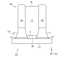
- FIG. 9 is a side view of a circuit board 200 including the multilayer ceramic capacitor 100.
- the circuit board 200 has a mounting board 210 on which the multilayer ceramic capacitor 100 is mounted.
- the mounting board 210 has a base material 211 that extends along a plane in the L direction and W direction and has a mounting surface G perpendicular to the T direction, and a pair of connection electrodes 212 provided on the mounting surface G.
- the external electrodes 20a, 20b of the multilayer ceramic capacitor 100 are each connected to a pair of connection electrodes 212 of the mounting board 210 via solder H.
- the multilayer ceramic capacitor 100 is fixed to and electrically connected to the mounting board 210.
- the multilayer ceramic capacitor 100 is prepared in a packaged state as a package 300 when mounted on a mounting substrate 210.
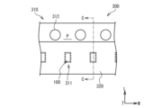
- Figures 10 and 11 are diagrams illustrating an example of the package 300.
- Figure 10 is a partial plan view of the package 300.
- Figure 11 is a cross-sectional view of the package 300 taken along line C-C in Figure 10.
- the package 300 includes a multilayer ceramic capacitor 100, a carrier tape 310, and a top tape 320.
- the carrier tape 310 is configured as a long tape extending in the W direction.
- the carrier tape 310 has a plurality of recesses 311 arranged at intervals in the W direction, each of which accommodates one of the multilayer ceramic capacitors 100.
- the carrier tape 310 has a sealing surface P, which is an upward surface perpendicular to the T direction, and the multiple recesses 311 are recessed downward in the T direction from the sealing surface P.
- the carrier tape 310 is configured so that the multilayer ceramic capacitors 100 in the multiple recesses 311 can be removed from the sealing surface P side.
- the carrier tape 310 has a plurality of feed holes 312 arranged at intervals in the W direction and penetrating in the T direction at positions offset in the L direction from the row of the plurality of recesses 311.
- the feed holes 312 are configured as engagement holes used by the tape transport mechanism to transport the carrier tape 310 in the W direction.
- the top tape 320 is attached to the seal surface P of the carrier tape 310 along the row of the recesses 311, and the recesses 311 housing the multilayer ceramic capacitors 100 are collectively covered by the top tape 320. This allows the multilayer ceramic capacitors 100 to be held within the recesses 311.
- the first main surface M1 of the laminated chip 10 facing upward in the T direction faces the top tape 320.
- the second main surface M2 of the laminated chip 10 facing downward in the T direction faces the bottom surface of the recess 311.
- the top tape 320 is peeled off from the seal surface P of the carrier tape 310 along the W direction. This allows the package 300 to sequentially open the multiple recesses 311 housing the multiple multilayer ceramic capacitors 100 upward in the T direction.
- the multilayer ceramic capacitor 100 housed in the open recess 311 is removed with the first main surface M1 of the multilayer chip 10 facing upward in the T direction being adsorbed to the tip of the suction nozzle of the mounting device.
- the mounting device moves the suction nozzle to move the multilayer ceramic capacitor 100 onto the mounting surface G of the mounting board 210.
- the mounting device places the second main surface M2 of the laminated chip 10 opposite the mounting surface G, aligns the external electrodes 20a, 20b on the pair of connection electrodes 212 to which the solder paste has been applied, and releases the suction nozzle from suction onto the first main surface M1 of the laminated chip 10. This places the laminated ceramic capacitor 100 on the mounting surface G.
- the solder paste is melted and then hardened using a reflow oven or the like on the mounting board 210 on which the multilayer ceramic capacitor 100 is placed on the mounting surface G.
- the external electrodes 20a, 20b are connected to the pair of connection electrodes 212 of the mounting board 210 via the solder H, thereby obtaining the circuit board 200 shown in FIG. 9.
- Second Embodiment 12(a) and 12(b) are partial cross-sectional perspective views of the multilayer ceramic capacitor 100a according to the second embodiment.
- the multilayer ceramic capacitor 100a differs from the multilayer ceramic capacitor 100 according to the first embodiment in the ratio of T 0 /W 0 .
- T 0 /W 0 is 1.3 times or more.
- the number of stacked internal electrode layers 12 can be increased, and therefore the capacitance can be increased. From the viewpoint of increasing the capacitance, it is preferable that T 0 /W 0 is 1.5 times or more.
- Third Embodiment 13(a) and 13(b) are partial cross-sectional perspective views of a multilayer ceramic capacitor 100b according to the third embodiment.
- the multilayer ceramic capacitor 100b differs from the multilayer ceramic capacitor 100 according to the first embodiment in that not all of the internal electrode layers 12 have the first region 121 and the second region 122, but some of the internal electrode layers 12 have the first region 121 and the second region 122.
- one or more internal electrode layers 12 have the first region 121 and the second region 122 from the outermost internal electrode layer 12 toward the inside.
- the internal electrode layer 12 having the first region 121 and the second region 122 is referred to as the internal electrode layer 12 in the outer region.
- the internal electrode layer 12 that is located inside the internal electrode layer 12 in the outer region and has a substantially constant dimension in the W direction is referred to as the internal electrode layer 12 in the inner region.
- the internal electrode layers 12 that make up a total of 10% or more of the total number of layers are the internal electrode layers 12 in the outer region, and it is more preferable that the internal electrode layers 12 that make up 25% or more of the total number of layers are the internal electrode layers 12 in the outer region.
- the internal electrode layers 12 that make up a total of 50% or less of the total number of layers are the internal electrode layers 12 in the outer region, and it is more preferable that the internal electrode layers 12 that make up 40% or less of the total number of layers are the internal electrode layers 12 in the outer region.
- the number of layers of the internal electrode layers 12 in the outer region on one side of the internal electrode layers 12 in the inner region in the T direction is the same as the number of layers of the internal electrode layers 12 in the outer region on the other side of the T direction.
- the capacitance can be increased by increasing the number of stacked internal electrode layers 12.
- T 0 /W 0 is preferably 1.3 times or more, and more preferably 1.5 times or more.
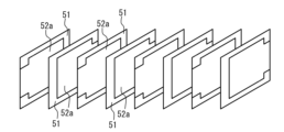
- the multilayer ceramic capacitor 100b according to this embodiment can be obtained, for example, by laminating a dielectric green sheet 51 on which an internal electrode pattern 52a having dimensions W1 and W2 is formed, and a dielectric green sheet 51 on which an internal electrode pattern 52 having a constant dimension in the W direction is formed, as illustrated in FIG. 14.
- Fourth Embodiment 15(a) and 15(b) are partial cross-sectional perspective views of a multilayer ceramic capacitor 100c according to the fourth embodiment.
- the multilayer ceramic capacitor 100c differs from the multilayer ceramic capacitor 100 according to the first embodiment in the lamination direction of the internal electrode layers 12.
- the W direction corresponds to the lamination direction of the internal electrode layers 12, and is the direction in which the upper and lower surfaces of the laminated chip 10 face each other.
- the T direction is the direction in which the two side surfaces of the laminated chip 10 face each other.
- the L direction is the direction in which the two end surfaces of the laminated chip 10 face each other. Therefore, in this embodiment, the dimension W1 in the first embodiment can be read as the dimension T1 in the T direction, and the dimension W2 can be read as the dimension T2 in the T direction.
- the multilayer ceramic capacitor 100c When the multilayer ceramic capacitor 100c is mounted on the mounting substrate 210, one of the two sides of the multilayer ceramic capacitor 100c faces the mounting substrate 210.
- circuit board 200 repeated electrostriction occurs in the multilayer ceramic capacitor 100c when an AC voltage is applied, which can cause vibrations in the thickness direction of the substrate 211 of the mounting board 210.
- vibrations generated in the substrate 211 become large, noise can be generated from the substrate 211, which is a phenomenon known as "ringing.”
- the lamination direction of the internal electrode layers 12 is the in-plane direction of the substrate 211, so that electrostriction of the laminated chip 10 is unlikely to cause vibration in the thickness direction of the substrate 211.
- the number of layers of the internal electrode layers 12 is small, and the amount of deformation due to electrostriction is kept small, so that even if vibration does occur in the substrate 211, it is unlikely to be large enough to cause noise.
- the multilayer ceramic capacitor 100d is different from the multilayer ceramic capacitor 100c according to the fourth embodiment in that not all of the internal electrode layers 12 have the first region 121 and the second region 122, but some of the internal electrode layers 12 have the first region 121 and the second region 122.
- one or more internal electrode layers 12 have the first region 121 and the second region 122 from the outermost internal electrode layer 12 toward the inside.
- the internal electrode layer 12 having the first region 121 and the second region 122 is referred to as the internal electrode layer 12 in the outer region.
- the internal electrode layer 12 that is located inside the internal electrode layer 12 in the outer region and has a substantially constant dimension in the T direction is referred to as the internal electrode layer 12 in the inner region.
- the internal electrode layers 12 that make up a total of 10% or more of the total number of layers are the internal electrode layers 12 in the outer region, and it is more preferable that the internal electrode layers 12 that make up 25% or more of the total number of layers are the internal electrode layers 12 in the outer region.
- the internal electrode layers 12 that make up a total of 50% or less of the total number of layers are the internal electrode layers 12 in the outer region, and it is more preferable that the internal electrode layers 12 that make up 40% or less of the total number of layers are the internal electrode layers 12 in the outer region.
- the number of layers of the internal electrode layers 12 in the outer region on one side in the W direction from the internal electrode layers 12 in the inner region is the same as the number of layers of the internal electrode layers 12 in the outer region on the other side in the W direction.
- the multilayer ceramic capacitor 100d When the multilayer ceramic capacitor 100d is mounted on the mounting substrate 210, one of the two sides of the multilayer ceramic capacitor 100d faces the mounting substrate 210.
- the circuit board 200 when the circuit board 200 is driven and a voltage is applied to the external electrodes 20a, 20b via the connection electrodes 212 of the mounting board 210, it is known that electrostriction occurs in the laminated chip 10 due to the piezoelectric effect.
- the electrostriction occurring in the laminated chip 10 causes a relatively large deformation in the lamination direction of the internal electrode layers 12.
- circuit board 200 repeated electrostriction occurs in the multilayer ceramic capacitor 100d when an AC voltage is applied, which can cause vibrations in the thickness direction of the substrate 211 of the mounting board 210.
- vibrations generated in the substrate 211 become large, noise can be generated from the substrate 211, which is a phenomenon known as "ringing.”
- the lamination direction of the internal electrode layers 12 is the in-plane direction of the substrate 211, so that electrostriction of the laminated chip 10 is unlikely to cause vibration in the thickness direction of the substrate 211.
- the number of layers of the internal electrode layers 12 is small, and the amount of deformation due to electrostriction is kept small, so that even if vibration does occur in the substrate 211, it is unlikely to be large enough to cause noise.
- FIG. 17 is an external view of the multilayer ceramic capacitor 100e according to the sixth embodiment.
- FIG. 18 is a cross-sectional view taken along line A-A in FIG. 17.
- FIG. 19 is a cross-sectional view taken along line B-B in FIG. 17.
- the multilayer ceramic capacitor 100e includes a laminated chip 10 having a substantially rectangular parallelepiped shape, and external electrodes 20a, 20b provided on two opposing end faces of the laminated chip 10. Of the four faces of the laminated chip 10 other than the two end faces, the two faces at both ends in the lamination direction are referred to as side faces.
- the two faces other than the two end faces and the two side faces are referred to as the upper face and the lower face.
- the lower face functions as a mounting face and faces the mounting substrate when the multilayer ceramic capacitor 100e is mounted on the mounting substrate.
- the external electrodes 20a, 20b extend to the upper face, the lower face, and the two side faces of the laminated chip 10. However, the external electrodes 20a and the external electrodes 20b are spaced apart from each other.
- the T direction (first direction) is the height direction of the multilayer ceramic capacitor 100e, and is the direction in which the upper and lower surfaces of the laminated chip 10 face each other.
- the W direction (second direction) is the stacking direction of the dielectric layers 11 and the internal electrode layers 12.
- the L direction (third direction) is the direction in which the two end faces of the laminated chip 10 face each other, and is the direction in which the external electrodes 20a and 20b face each other.
- the L direction, W direction, and T direction are mutually perpendicular.
- the laminated chip 10 has a configuration in which dielectric layers 11 containing a ceramic material that functions as a dielectric and internal electrode layers 12 mainly composed of metal are alternately laminated.
- the laminated chip 10 has a plurality of internal electrode layers 12 facing each other and a dielectric layer 11 sandwiched between the plurality of internal electrode layers 12.
- the edges in the direction in which each internal electrode layer 12 extends are alternately exposed to the first end face on which the external electrode 20a of the laminated chip 10 is provided and the second end face on which the external electrode 20b is provided.
- the internal electrode layer 12 connected to the external electrode 20a is not connected to the external electrode 20b.
- the internal electrode layer 12 connected to the external electrode 20b is not connected to the external electrode 20a.
- each internal electrode layer 12 is alternately conductive to the external electrode 20a and the external electrode 20b.
- the internal electrode layer 12 is disposed on the top layer in the lamination direction, and the internal electrode layer 12 is also disposed on the bottom layer in the lamination direction, and each of the two side surfaces of the laminate is covered with a cover layer 13.
- the cover layer 13 is mainly composed of a ceramic material.
- the main component of the cover layer 13 is the same as the main component of the dielectric layer 11.
- the dielectric layer 11 has a main phase of a ceramic material having a perovskite structure represented by the general formula ABO 3.
- the perovskite structure includes ABO 3- ⁇ , which is not a stoichiometric composition.
- the ceramic material can be selected from at least one of BaTiO 3 (barium titanate), CaZrO 3 (calcium zirconate), CaTiO 3 (calcium titanate), SrTiO 3 (strontium titanate), MgTiO 3 (magnesium titanate), Ba 1-x-y Ca x Sr y Ti 1-z Zr z O 3 (0 ⁇ x ⁇ 1, 0 ⁇ y ⁇ 1, 0 ⁇ z ⁇ 1) that forms a perovskite structure, and the like.
- Ba1 -xyCaxSryTi1 - zZrzO3 is barium strontium titanate, barium calcium titanate, barium zirconate, barium zirconate titanate, calcium zirconate titanate and barium calcium zirconate titanate, etc.
- the dielectric layer 11 may contain additives.
- additives to the dielectric layer 11 include oxides of magnesium (Mg), manganese (Mn), molybdenum (Mo), vanadium (V), chromium (Cr), rare earth elements (yttrium (Y), samarium (Sm), europium (Eu), gadolinium (Gd), terbium (Tb), dysprosium (Dy), holmium (Ho), erbium (Er), thulium (Tm), and ytterbium (Yb)), or oxides containing cobalt (Co), nickel (Ni), lithium (Li), boron (B), sodium (Na), potassium (K), or silicon (Si), or glasses containing Co, Ni, Li, B, Na, K, or Si.
- each dielectric layer 11 in the T direction is, for example, 0.3 ⁇ m or more and 3 ⁇ m or less.
- the thickness of each dielectric layer 11 in the T direction can be measured by exposing the cross section of the multilayer ceramic capacitor 100e, for example, as shown in FIG. 18, by mechanical polishing, and then obtaining the average thickness value at 10 points from an image taken by a microscope such as a scanning transmission electron microscope.
- the internal electrode layer 12 is mainly composed of Ni.
- the thickness of each internal electrode layer 12 in the T direction is, for example, 0.1 ⁇ m or more and 2 ⁇ m or less.
- the thickness of each internal electrode layer 12 in the T direction can be measured by exposing the cross section of the multilayer ceramic capacitor 100e, for example, as shown in FIG. 18, by mechanical polishing, and then obtaining the average thickness value at 10 points from an image taken by a microscope such as a scanning transmission electron microscope.
- the region where the internal electrode layer 12 connected to the external electrode 20a and the internal electrode layer 12 connected to the external electrode 20b face each other is a region that generates capacitance in the multilayer ceramic capacitor 100e. Therefore, this region that generates capacitance is referred to as the capacitance section 14.
- the capacitance section 14 is a region where adjacent internal electrode layers connected to different external electrodes face each other.
- the region where the internal electrode layers 12 connected to the external electrode 20a face each other without an internal electrode layer 12 connected to the external electrode 20b being interposed therebetween is called the end margin 15.
- the region where the internal electrode layers 12 connected to the external electrode 20b face each other without an internal electrode layer 12 connected to the external electrode 20a being interposed therebetween is also the end margin 15.
- the end margin is the region where the internal electrode layers connected to the same external electrode face each other without an internal electrode layer connected to a different external electrode being interposed therebetween.
- the end margin 15 is a region that does not generate capacitance.
- the end margin 15 may have the same composition as the dielectric layer 11 of the capacitance section 14, or may have a different composition.
- the region extending from the upper surface to the internal electrode layer 12 in the T direction and the region extending from the lower surface to the internal electrode layer 12 in the T direction are referred to as the side margin 16.
- the side margin 16 is a region provided to cover the ends of the multiple internal electrode layers 12 stacked in the laminated structure that extend to the upper and lower surfaces.
- the side margin 16 is also a region that does not generate capacitance.
- the side margin 16 may have the same composition as the dielectric layer 11 of the capacitance section 14, or a different composition.
- the external electrode 20a is an enlarged cross-sectional view of the vicinity of the external electrode 20a. Hatching is omitted in FIG. 20.
- the external electrode 20a has a structure in which a plating layer 22 is provided on an underlayer 21.
- the underlayer 21 is mainly composed of Cu.
- the underlayer 21 may also contain a glass component.
- the plating layer 22 is mainly composed of a metal such as Ni, aluminum (Al), zinc (Zn), Sn, or an alloy of two or more of these.
- the plating layer 22 may be a plating layer of a single metal component, or may be a plurality of plating layers of different metal components.
- the plating layer 22 has a structure in which a first plating layer 23, a second plating layer 24, and a third plating layer 25 are formed in this order from the underlayer 21 side.
- the first plating layer 23 is, for example, a Sn plating layer.
- the second plating layer 24 is, for example, a Ni plating layer.
- the third plating layer 25 is, for example, a Sn plating layer. Note that while FIG. 20 illustrates the external electrode 20a, the external electrode 20b also has a similar layered structure.
- Increasing the total opposing area of the internal electrode layers is important when trying to realize a large-capacity multilayer ceramic capacitor.
- the total opposing area of the internal electrode layers 12 increases, which is thought to enable the realization of a large capacity.
- misalignment is more likely to occur during stacking, and it becomes difficult to cut the pre-fired laminate perpendicular to the stacking direction.
- the multilayer ceramic capacitor 100e has a configuration in which the area of each internal electrode layer is increased and the number of layers is reduced. Specifically, as illustrated in FIG. 17, when the height of the multilayer ceramic capacitor 100e in the T direction is height T0 , the width in the W direction is width W0 , and the length in the L direction is length L0 , the multilayer ceramic capacitor 100e has a relationship of T0 ⁇ W0 ⁇ 1.3. With this configuration, the width of the internal electrode layers 12 can be increased while the number of layers of the internal electrode layers 12 can be reduced, so that positional deviation during stacking can be suppressed and the pre-fired laminate can be cut perpendicular to the stacking direction. Note that the height T0 , width W0 , and length L0 are the maximum dimensions in the T direction, W direction, and L direction, respectively.
- the binder may not be sufficiently removed because the binder discharge path becomes long.
- the decomposition gas of the binder may remain inside the laminate, which may cause cracks (de-by-cracks) or delamination.
- the multilayer ceramic capacitor 100e according to this embodiment has a configuration that can achieve good binder removal properties even in a configuration in which the relationship T 0 ⁇ W 0 ⁇ 1.3 is established.
- a low-melting-point metal with a lower melting point than Cu, the main component of the underlayer 21, is provided inside the internal electrode layer 12 or at the interface between the internal electrode layer 12 and the dielectric layer 11.
- the low-melting-point metal is not particularly limited as long as it has a melting point lower than Cu, but examples include Ga (gallium), In (indium), Sn, Bi (bismuth), Pb (lead), and Zn.
- the low-melting-point metal may be alloyed with Ni, the main component of the internal electrode layer 12, or may be disposed as a single metal.
- the low-melting-point metal may be disposed uniformly dispersed in the internal electrode layer 12, or may be segregated at the interface between the internal electrode layer 12 and the dielectric layer 11.
- the binder ejection start temperature is lower during the heat treatment in the binder removal process compared to when the low melting point metal is not provided. This achieves good binder removal properties and makes it possible to suppress cracks and delamination.
- the binder ejection start temperature is lower because the low melting point metal melts at the binder ejection temperature, thereby making it easier to eject the binder.
- the concentration of the low melting point metal is preferably 0.1 at% or more, more preferably 0.3 at% or more, and even more preferably 0.5 at% or more.
- the concentration of the low melting point metal refers to the amount of low melting point metal added (at%) in the entire one internal electrode layer 12 sandwiched between two adjacent dielectric layers, when the Ni of the internal electrode layer 12 is 100 at%.
- the concentration of the low melting point metal refers to the total amount of the multiple types of low melting point metals.
- the concentration of the low-melting metal added is preferably 10 at% or less, more preferably 5 at% or less, and even more preferably 2 at% or less.
- the height T0 , width W0 , and length L0 are not particularly limited, but for example, the height T0 can be 0.15 mm or more and 1.0 mm or less, the width W0 can be 0.1 mm or more and 0.7 mm or less, and the length L0 can be 0.2 mm or more and 1.2 mm or less.
- the stacking density of the internal electrode layers 12 is, for example, 500 layers/mm or more, 750 layers/mm or more, or 1000 layers/mm or more and 1500 layers/mm or less.
- T 0 is preferably 1.5 times or more, and more preferably 2.0 times or more, of W 0 .
- T a is 500 times or more, 700 times or more, or 1000 times or more of W a .
- W ratio is, for example, 1.3 times or more, 1.5 times or more, or 2.0 times or more.
- Figure 23 is a diagram illustrating the flow of the method for manufacturing the multilayer ceramic capacitor 100e.
- a dielectric material for forming the dielectric layer 11 is prepared.
- the A-site elements and B-site elements contained in the dielectric layer 11 are usually contained in the dielectric layer 11 in the form of a sintered body of ABO3 particles.
- BaTiO3 is a tetragonal compound having a perovskite structure and exhibits a high dielectric constant. This BaTiO3 can generally be obtained by reacting a titanium raw material such as titanium dioxide with a barium raw material such as barium carbonate to synthesize barium titanate.
- a predetermined additive compound is added to the obtained ceramic powder according to the purpose.
- the additive compound may be an oxide of Mg, Mn, Mo, V, Cr, or a rare earth element (Y, Sm, Eu, Gd, Tb, Dy, Ho, Er, Tm, or Yb), or an oxide containing Co, Ni, Li, B, Na, K, or Si, or a glass containing Co, Ni, Li, B, Na, K, or Si.
- SiO2 mainly functions as a sintering aid.
- a compound containing an additive compound is wet mixed with a ceramic raw material powder, and then dried and pulverized to prepare a ceramic material.
- the ceramic material obtained as described above may be pulverized as necessary to adjust the particle size, or may be combined with a classification process to adjust the particle size. Through the above steps, a dielectric material is obtained.
- a binder such as polyvinyl butyral (PVB) resin, an organic solvent such as ethanol or toluene, and a plasticizer are added to the obtained raw material powder and wet mixed.
- a dielectric green sheet is coated on a substrate by, for example, a die coater method or a doctor blade method, and then dried.
- the substrate is, for example, a polyethylene terephthalate (PET) film.
- an internal electrode pattern 52 is formed on a dielectric green sheet 51.
- the dielectric green sheet 51 on which the internal electrode pattern 52 is formed is used as a lamination unit.
- Ni powder containing a low-melting point metal with a lower melting point than Cu is used for the internal electrode pattern 52.
- the film formation method may be printing, sputtering, vapor deposition, etc.
- cover sheets 53 e.g., 2 to 10 layers are stacked on top and bottom of the laminate obtained by stacking the lamination units, and are thermocompression bonded.
- the cover sheets 53 can be formed by the same method as the dielectric green sheet 51.
- the laminate thus obtained is subjected to a debindering treatment in a N2 atmosphere at a heat treatment temperature of about 250° C. to 700° C. for a heat treatment time of about 5 minutes to 1 hour.
- the laminated chip 10 is sintered in a reducing atmosphere with an oxygen partial pressure of 10 ⁇ 5 to 10 ⁇ 8 atm at 1100° C. to 1300° C. for 10 minutes to 2 hours.
- a re-oxidation treatment may be performed at 600° C. to 1000° C. in a N 2 gas atmosphere.
- a metal paste that will become the underlayer 21 is applied to the first side surface of the laminate by a dipping method or the like.
- This metal paste contains a glass component such as glass frit.
- the metal paste is baked at a temperature of about 700° C. to 900° C. to form the underlayer 21 .
- a metal coating such as copper, nickel, or tin may be applied to the underlayer 21 by a plating process.
- the first plating layer 23, the second plating layer 24, and the third plating layer 25 are formed in this order on the underlayer 21. This completes the multilayer ceramic capacitor 100e.
- a low melting point metal is added to the internal electrode pattern 52.
- the binder ejection start temperature during the heat treatment in the binder removal process becomes lower than when the low melting point metal is not added. This achieves good binder removal characteristics and makes it possible to suppress cracks and delamination.
- the base layer 21 is baked after the laminated chip 10 is baked, but this is not limited to the above.
- the base layer 21 may be baked at the same time as the laminated chip 10 is baked.
- FIG 25 is a side view of a circuit board 200 including the multilayer ceramic capacitor 100e.
- the circuit board 200 has a mounting board 210 on which the multilayer ceramic capacitor 100e is mounted.
- the mounting board 210 has a base material 211 that extends along a plane in the L direction and W direction and has a mounting surface G perpendicular to the T direction, and a pair of connection electrodes 212 provided on the mounting surface G.
- the external electrodes 20a, 20b of the multilayer ceramic capacitor 100e are each connected to a pair of connection electrodes 212 of the mounting board 210 via solder H.
- the multilayer ceramic capacitor 100e is fixed to and electrically connected to the mounting board 210.
- circuit board 200 repeated electrostriction occurs in the multilayer ceramic capacitor 100e when an AC voltage is applied, which can cause vibrations in the thickness direction of the substrate 211 of the mounting board 210.
- vibrations generated in the substrate 211 become large, noise can be generated from the substrate 211, which is a phenomenon known as "ringing.”
- the lamination direction of the internal electrode layers 12 is the in-plane direction of the substrate 211, so that electrostriction of the laminated chip 10 is unlikely to cause vibration in the thickness direction of the substrate 211.
- the number of layers of the internal electrode layers 12 is small, and the amount of deformation due to electrostriction is kept small, so that even if vibration does occur in the substrate 211, it is unlikely to be large enough to cause noise.
- the multilayer ceramic capacitor 100e is prepared in a packaged state as a package 300 when mounted on the mounting substrate 210.
- Figures 26 and 27 are diagrams illustrating the package 300.
- Figure 26 is a partial plan view of the package 300.
- Figure 27 is a cross-sectional view of the package 300 taken along line D-D in Figure 26.
- the package 300 includes a multilayer ceramic capacitor 100e, a carrier tape 310, and a top tape 320.
- the carrier tape 310 is configured as a long tape extending in the W direction.
- the carrier tape 310 has a plurality of recesses 311 arranged at intervals in the W direction, each of which accommodates one of the multilayer ceramic capacitors 100e.
- the carrier tape 310 has a sealing surface P, which is an upward surface perpendicular to the T direction, and the multiple recesses 311 are recessed downward in the T direction from the sealing surface P.
- the carrier tape 310 is configured so that the multilayer ceramic capacitors 100e in the multiple recesses 311 can be removed from the sealing surface P side.
- the carrier tape 310 has a plurality of feed holes 312 arranged at intervals in the W direction and penetrating in the T direction at positions offset in the L direction from the row of the plurality of recesses 311.
- the feed holes 312 are configured as engagement holes used by the tape transport mechanism to transport the carrier tape 310 in the W direction.
- the top tape 320 is attached to the seal surface P of the carrier tape 310 along the row of the recesses 311, and the recesses 311 housing the multilayer ceramic capacitors 100e are collectively covered by the top tape 320. This allows the multilayer ceramic capacitors 100e to be held within the recesses 311.
- the first main surface M1 of the laminated chip 10 facing upward in the T direction faces the top tape 320.
- the second main surface M2 of the laminated chip 10 facing downward in the T direction faces the bottom surface of the recess 311.
- the top tape 320 is peeled off from the seal surface P of the carrier tape 310 along the W direction. This allows the package 300 to sequentially open the multiple recesses 311 housing the multiple multilayer ceramic capacitors 100e upward in the T direction.
- the multilayer ceramic capacitor 100e housed in the opened recess 311 is removed with the first main surface M1 of the multilayer chip 10 facing upward in the T direction being adsorbed to the tip of the suction nozzle of the mounting device.
- the mounting device moves the suction nozzle to move the multilayer ceramic capacitor 100e onto the mounting surface G of the mounting board 210.
- the mounting device places the second main surface M2 of the laminated chip 10 facing the mounting surface G, aligns the external electrodes 20a, 20b on the pair of connection electrodes 212 to which the solder paste has been applied, and releases the suction nozzle from suctioning the first main surface M1 of the laminated chip 10. This places the laminated ceramic capacitor 100e on the mounting surface G.
- the solder paste is melted and then hardened using a reflow oven or the like on the mounting board 210 on which the multilayer ceramic capacitor 100e is placed on the mounting surface G.
- the external electrodes 20a, 20b are connected to the pair of connection electrodes 212 of the mounting board 210 via the solder H, and the circuit board 200 shown in FIG. 25 is obtained.
- Fig. 28 is a view corresponding to the cross section along the line CC in Fig. 17.
- the dimensions of each internal electrode layer 12 in the T direction are varied.
- the internal electrode layer 12 connected to the external electrode 20a has a first region 121 (connection portion) connected to the external electrode 20a in a region corresponding to the end margin 15 and having a dimension T1 in the T direction, and a second region 122 having a dimension T2 in the T direction in a region corresponding to the capacitance portion 14.
- the dimension T1 is lower than the dimension T2.
- the first region 121 is located inside the second region 122.
- the internal electrode layer 12 connected to the external electrode 20b also has a first region 121 having a dimension T1 and a second region 122 having a dimension T2.
- T1/T2 is preferably 1/2 or more, and more preferably 2/3 or more. Furthermore, T1/T2 is preferably 4/5 or less, and more preferably 3/4 or less.
- the dimension of the external electrodes 20a, 20b extending in the L direction from both end faces of the laminated chip 10 is referred to as dimension e.
- the dimension of the first region 121 in the L direction is 1/3 or more of dimension e, and more preferably 1/2 or more.
- the multilayer ceramic capacitor 100f according to this embodiment can be obtained, for example, by stacking dielectric green sheets 51 on which internal electrode patterns 52a having dimensions T1 and T2 are formed, as illustrated in FIG. 31.
- all the internal electrode layers 12 have the first region 121 and the second region 122, but some of the internal electrode layers 12 may have the first region 121 and the second region 122.
- the internal electrode layer 12 having the first region 121 and the second region 122 is referred to as the internal electrode layer 12 in the outer region.
- the internal electrode layer 12 that is located inside the internal electrode layer 12 in the outer region and has a substantially constant height in the T direction is referred to as the internal electrode layer 12 in the inner region.
- the internal electrode layers 12 that make up a total of 10% or more of the total number of layers are the internal electrode layers 12 in the outer region, and it is more preferable that the internal electrode layers 12 that make up 25% or more of the total number of layers are the internal electrode layers 12 in the outer region.
- the internal electrode layers 12 that make up a total of 50% or less of the total number of layers are the internal electrode layers 12 in the outer region, and it is more preferable that the internal electrode layers 12 that make up 40% or less of the total number of layers are the internal electrode layers 12 in the outer region.
- the number of layers of the internal electrode layers 12 in the outer region on one side in the W direction from the internal electrode layers 12 in the inner region is the same as the number of layers of the internal electrode layers 12 in the outer region on the other side in the W direction.
- the multilayer ceramic capacitor 100g according to this embodiment can be obtained, for example, by laminating a dielectric green sheet 51 on which an internal electrode pattern 52a having dimensions T1 and T2 is formed, and a dielectric green sheet 51 on which an internal electrode pattern 52 having a constant dimension in the T direction is formed, as illustrated in FIG. 33.
- a multilayer ceramic capacitor has been described as an example of a ceramic electronic component, but the present invention is not limited to this.
- the configuration of each of the above embodiments can also be applied to other multilayer ceramic electronic components, such as varistors and thermistors.
- the multilayer ceramic capacitors according to each embodiment were fabricated and their characteristics were investigated.
- Example 1 the multilayer ceramic capacitor described in the first embodiment was produced. First, a slurry mainly composed of BaTiO3 was mixed and coated to obtain a dielectric green sheet. An internal electrode pattern was printed on each dielectric green sheet. Nickel powder was used for the internal electrode pattern, and Sn powder was added. The concentration of Sn added to Ni was 1.0 at%. 250 layers of the obtained laminate unit were laminated to obtain a laminate.
- a slurry mainly composed of BaTiO 3 was mixed and applied to obtain a cover sheet.
- a plurality of cover sheets were laminated and pressed on the top and bottom of the laminate in the lamination direction, and then a binder removal process was performed. Then, the laminate was fired and reoxidized.
- a metal paste mainly composed of Cu was applied to two end faces of the obtained laminated chip and baked at about 800°C. Through these processes, a multilayer ceramic capacitor was produced in which 250 internal electrode layers were laminated, with a length L 0 of 0.6 mm, a width W 0 of 0.3 mm, and a height T 0 of 0.3 mm.
- each internal electrode layer in the T direction was 0.5 ⁇ m, and the thickness of each dielectric layer in the T direction was 0.5 ⁇ m.
- the thickness of each cover layer in the T direction was 25 ⁇ m.
- the thickness of each side margin in the W direction was 25 ⁇ m.
- the dimension W2 in the W direction was made larger in the capacitive section, and the dimension W1 in the W direction in the end margin was made smaller than W2.
- the dimension W2 of the internal electrode layer in the capacitive section was 250 ⁇ m, and the dimension W1 of the internal electrode layer in the end margin was 150 ⁇ m.
- the length in the L direction of each end margin was 15 ⁇ m.
- the dimension e of each external electrode extending in the L direction from both end faces of the multilayer chip was 20 ⁇ m.
- Example 2-1 the multilayer ceramic capacitor described in the second embodiment was produced.
- the number of stacked internal electrode layers was 350.
- the length L0 was 0.6 mm
- the width W0 was 0.3 mm
- the height T0 was 0.4 mm.
- the other conditions were the same as those in Example 1.
- Example 2-2 the multilayer ceramic capacitor described in the second embodiment was produced.
- the number of stacked internal electrode layers was 450.
- the length L0 was 0.6 mm
- the width W0 was 0.3 mm
- the height T0 was 0.5 mm.
- the other conditions were the same as those of Example 1.
- Example 3 In Example 3, the multilayer ceramic capacitor described in the third embodiment was fabricated.
- the number of layers of the internal electrode layers was 450.
- the length L 0 was 0.6 mm
- the width W 0 was 0.3 mm
- the height T 0 was 0.5 mm.
- the dimension W2 in the W direction was made larger in the capacitance section
- the dimension W1 in the W direction was made smaller than W2 in the end margin.
- the dimension W2 of the internal electrode layer in the capacitance section was 250 ⁇ m
- the dimension W1 of the internal electrode layer in the end margin was 150 ⁇ m.
- the dimension in the W direction of the internal electrode layer in the capacitance section and the dimension in the W direction of the internal electrode layer in the end margin were 250 ⁇ m.
- Other conditions were the same as in Example 1.
- Example 4-1 In Example 4-1, the multilayer ceramic capacitor described in the fourth embodiment was fabricated.
- the number of layers of the internal electrode layers was 250.
- the length L 0 was 0.6 mm
- the width W 0 was 0.3 mm
- the height T 0 was 0.5 mm.
- the thickness of each internal electrode layer in the W direction was 0.5 ⁇ m
- the thickness of each dielectric layer in the W direction was 0.5 ⁇ m.
- the thickness of each cover layer in the W direction was 25 ⁇ m.
- the thickness of each side margin in the T direction was 25 ⁇ m.
- the dimension T2 in the T direction was made larger in the capacitance section
- the dimension T1 in the T direction was made smaller than T2 in the end margin.
- the dimension T2 of the internal electrode layer in the capacitance section was 450 ⁇ m, and the dimension T1 of the internal electrode layer in the end margin was 300 ⁇ m.
- the length of each end margin in the L direction was 15 ⁇ m.
- the dimension e of each external electrode extending in the L direction from both end faces of the laminated chip was 20 ⁇ m.
- Example 4-2 In Example 4-2, the multilayer ceramic capacitor described in the fourth embodiment was fabricated.
- the number of layers of the internal electrode layers was 250.
- the length L 0 was 0.6 mm
- the width W 0 was 0.3 mm
- the height T 0 was 0.4 mm.
- the thickness of each internal electrode layer in the W direction was 0.5 ⁇ m
- the thickness of each dielectric layer in the W direction was 0.5 ⁇ m.
- the thickness of each cover layer in the W direction was 25 ⁇ m.
- the thickness of each side margin in the T direction was 25 ⁇ m.
- the dimension T2 in the T direction was made larger in the capacitance section
- the dimension T1 in the T direction was made smaller than T2 in the end margin.
- the dimension T2 of the internal electrode layer in the capacitance section was 350 ⁇ m, and the dimension T1 of the internal electrode layer in the end margin was 250 ⁇ m.
- the length of each end margin in the L direction was 15 ⁇ m.
- the dimension e of each external electrode extending in the L direction from both end faces of the laminated chip was 20 ⁇ m.
- Example 5 the multilayer ceramic capacitor described in the fifth embodiment was produced.
- the dimension T2 in the T direction was made larger in the capacitive section, and the dimension T1 in the T direction was made smaller than T2 in the end margin.
- the dimension T2 of the internal electrode layer in the capacitive section was 450 ⁇ m, and the dimension T1 of the internal electrode layer in the end margin was 300 ⁇ m.
- the dimension in the T direction of the internal electrode layer in the capacitive section and the dimension in the T direction of the internal electrode layer in the end margin were 450 ⁇ m.
- Other conditions were the same as in Example 4.
- Table 1 shows the conditions for Examples 1 to 5 and Comparative Examples 1 and 2.
- Example 6 the multilayer ceramic capacitor described in the sixth embodiment was produced.
- a slurry mainly composed of BaTiO3 was mixed and coated to obtain a dielectric green sheet.
- An internal electrode pattern was printed on each dielectric green sheet.
- Nickel powder was used for the internal electrode pattern, and Sn powder was added.
- the concentration of Sn added to Ni was 1.0 at%.
- the height of each internal electrode pattern was made lower than the height of the dielectric green sheet. 250 layers of the obtained laminate unit were laminated to obtain a laminate.
- a slurry mainly composed of BaTiO 3 was mixed and applied to obtain a cover sheet.
- a plurality of cover sheets were laminated and pressed on the top and bottom of the laminate in the lamination direction, and then barrel polishing and a binder removal process were performed. Then, the laminate was fired and reoxidized.
- a metal paste mainly composed of Cu was applied to two end faces of the obtained laminated chip and baked at about 800 ° C. Through these processes, a multilayer ceramic capacitor was produced in which the internal electrode layers were laminated in 250 layers, with a length L 0 of 0.6 mm, a width W 0 of 0.3 mm, and a height T 0 of 0.5 mm.
- each internal electrode layer in the W direction was 0.5 ⁇ m
- the thickness of each dielectric layer in the W direction was 0.5 ⁇ m
- the thickness of each cover layer in the W direction was 25 ⁇ m.
- the thickness of each side margin in the T direction was 25 ⁇ m.
- the length of each end margin in the L direction was 40 ⁇ m.
- Example 7 In Example 7, the multilayer ceramic capacitor described in the seventh embodiment was fabricated. In each internal electrode layer, the dimension T2 in the T direction was made larger in the capacitance section, and the dimension T1 in the T direction was made smaller than T2 in the end margin. The dimension T2 of the internal electrode layer in the capacitance section was 450 ⁇ m, and the dimension T1 of the internal electrode layer in the end margin was 300 ⁇ m. The other conditions were the same as in Example 6.
- Example 8 In Example 8, the multilayer ceramic capacitor described in the eighth embodiment was fabricated. In each of the 50 internal electrode layers in the outer region, the dimension T2 in the T direction was made larger in the capacitive portion, and the dimension T1 in the T direction was made smaller than T2 in the end margin. The dimension T2 of the internal electrode layer in the capacitive portion was 450 ⁇ m, and the dimension T1 of the internal electrode layer in the end margin was 300 ⁇ m. In each of the 150 internal electrode layers in the inner region, the dimension T2 of the internal electrode layer in the capacitive portion and the dimension T1 in the end margin were 450 ⁇ m. The other conditions were the same as in Example 6.
- Example 9 the printing width of the internal electrode pattern was changed from that of Example 6 so that the dimension of each internal electrode layer in the T direction was 350 ⁇ m, and a multilayer ceramic capacitor was produced in which 250 internal electrode layers were laminated, with a length L 0 of 0.6 mm, a width W 0 of 0.3 mm, and a height T 0 of 0.4 mm. Other conditions were the same as in Example 6.
- Table 3 shows the conditions for Examples 6 to 9 and Comparative Example 3.
Landscapes
- Engineering & Computer Science (AREA)
- Power Engineering (AREA)
- Microelectronics & Electronic Packaging (AREA)
- Manufacturing & Machinery (AREA)
- Fixed Capacitors And Capacitor Manufacturing Machines (AREA)
- Ceramic Capacitors (AREA)
Abstract
La présente invention concerne un composant électronique en céramique qui est caractérisé en ce qu'il comprend : une puce stratifiée qui a une forme parallélépipédique sensiblement rectangulaire, qui a stratifié en alternance une pluralité de couches diélectriques et une pluralité de couches d'électrode interne principalement constituées de Ni, et qui est formée de telle sorte que les couches d'électrode interne sont exposées en alternance à des première et seconde surfaces d'extrémité opposées de la forme parallélépipédique sensiblement rectangulaire; et une paire d'électrodes externes qui sont disposées sur les première et seconde surfaces d'extrémité et qui ont des couches de contact qui sont en contact avec les première et seconde surfaces d'extrémité et qui sont principalement constituées de Cu. Le composant électronique en céramique est également caractérisé en ce qu'un métal à bas point de fusion ayant un point de fusion inférieur à celui de Cu est ajouté aux couches d'électrode interne et aux couches de contact, et dans une ou plusieurs des couches d'électrode interne à partir de la couche la plus à l'extérieur des couches d'électrode interne, la largeur des parties de connexion connectées aux électrodes externes est inférieure à celle dans d'autres régions.
Applications Claiming Priority (4)
| Application Number | Priority Date | Filing Date | Title |
|---|---|---|---|
| JP2022158955 | 2022-09-30 | ||
| JP2022158517 | 2022-09-30 | ||
| JP2022-158517 | 2022-09-30 | ||
| JP2022-158955 | 2022-09-30 |
Publications (1)
| Publication Number | Publication Date |
|---|---|
| WO2024071420A1 true WO2024071420A1 (fr) | 2024-04-04 |
Family
ID=90478208
Family Applications (1)
| Application Number | Title | Priority Date | Filing Date |
|---|---|---|---|
| PCT/JP2023/035788 WO2024071420A1 (fr) | 2022-09-30 | 2023-09-29 | Composant électronique en céramique, boîtier, carte de circuit imprimé et procédé de fabrication de composant électronique en céramique |
Country Status (1)
| Country | Link |
|---|---|
| WO (1) | WO2024071420A1 (fr) |
Citations (4)
| Publication number | Priority date | Publication date | Assignee | Title |
|---|---|---|---|---|
| JP2012099786A (ja) * | 2010-10-29 | 2012-05-24 | Samsung Electro-Mechanics Co Ltd | 積層型セラミックキャパシタ及びその製造方法 |
| JP2014112647A (ja) * | 2012-11-05 | 2014-06-19 | Murata Mfg Co Ltd | 積層セラミック電子部品、その製造方法、テーピング電子部品連、その製造方法、および積層セラミック電子部品の方向識別方法 |
| JP2022067608A (ja) * | 2020-10-20 | 2022-05-06 | サムソン エレクトロ-メカニックス カンパニーリミテッド. | 積層型電子部品 |
| JP2022133147A (ja) * | 2021-03-01 | 2022-09-13 | 太陽誘電株式会社 | セラミック電子部品およびその製造方法 |
-
2023
- 2023-09-29 WO PCT/JP2023/035788 patent/WO2024071420A1/fr unknown
Patent Citations (4)
| Publication number | Priority date | Publication date | Assignee | Title |
|---|---|---|---|---|
| JP2012099786A (ja) * | 2010-10-29 | 2012-05-24 | Samsung Electro-Mechanics Co Ltd | 積層型セラミックキャパシタ及びその製造方法 |
| JP2014112647A (ja) * | 2012-11-05 | 2014-06-19 | Murata Mfg Co Ltd | 積層セラミック電子部品、その製造方法、テーピング電子部品連、その製造方法、および積層セラミック電子部品の方向識別方法 |
| JP2022067608A (ja) * | 2020-10-20 | 2022-05-06 | サムソン エレクトロ-メカニックス カンパニーリミテッド. | 積層型電子部品 |
| JP2022133147A (ja) * | 2021-03-01 | 2022-09-13 | 太陽誘電株式会社 | セラミック電子部品およびその製造方法 |
Similar Documents
| Publication | Publication Date | Title |
|---|---|---|
| CN109559892B (zh) | 陶瓷电子器件和陶瓷电子器件的制造方法 | |
| JP7227690B2 (ja) | 積層セラミックコンデンサおよびその製造方法 | |
| JP7290914B2 (ja) | 積層セラミックコンデンサの製造方法 | |
| JP7348890B2 (ja) | セラミック電子部品およびその製造方法 | |
| JP2019212746A (ja) | セラミック電子部品およびその製造方法 | |
| JP2021082686A (ja) | セラミック電子部品およびその製造方法 | |
| US11862397B2 (en) | Ceramic electronic device and manufacturing method of the same | |
| US20200402719A1 (en) | Ceramic electronic device and manufacturing method of the same | |
| US20230223196A1 (en) | Multilayer ceramic electronic device and manufacturing method of the same | |
| JP2021061289A (ja) | セラミック電子部品の製造方法、およびカバーシート | |
| WO2024071420A1 (fr) | Composant électronique en céramique, boîtier, carte de circuit imprimé et procédé de fabrication de composant électronique en céramique | |
| JP2020031161A (ja) | 積層セラミックコンデンサおよびその製造方法 | |
| WO2024070485A1 (fr) | Composant électronique en céramique et son procédé de fabrication | |
| JP2021103730A (ja) | セラミック電子部品および実装基板 | |
| WO2024079966A1 (fr) | Composant électronique céramique multicouche | |
| JP2021080113A (ja) | セラミック原料粉末、誘電体グリーンシート、セラミック原料粉末の製造方法、およびセラミック電子部品の製造方法 | |
| US20230043869A1 (en) | Ceramic electronic device and manufacturing method of the same | |
| US11315731B2 (en) | Ceramic electronic device and manufacturing method of the same | |
| US20230070005A1 (en) | Ceramic electronic device and manufacturing method of the same | |
| WO2024101311A1 (fr) | Composant électronique en céramique et son procédé de fabrication | |
| US20220277897A1 (en) | Ceramic electronic device, powder material, paste material, and manufacturing method of ceramic electronic device | |
| WO2024101307A1 (fr) | Composant électronique en céramique et procédé de fabrication associé | |
| WO2024070416A1 (fr) | Composant électronique en céramique, et procédé de fabrication de celui-ci | |
| US20220059288A1 (en) | Multilayer ceramic capacitor | |
| JP2024062064A (ja) | セラミック電子部品およびその製造方法 |
Legal Events
| Date | Code | Title | Description |
|---|---|---|---|
| 121 | Ep: the epo has been informed by wipo that ep was designated in this application |
Ref document number: 23872639 Country of ref document: EP Kind code of ref document: A1 |