WO2024071420A1 - Ceramic electronic component, package, circuit board, and method for manufacturing ceramic electronic component - Google Patents
Ceramic electronic component, package, circuit board, and method for manufacturing ceramic electronic component Download PDFInfo
- Publication number
- WO2024071420A1 WO2024071420A1 PCT/JP2023/035788 JP2023035788W WO2024071420A1 WO 2024071420 A1 WO2024071420 A1 WO 2024071420A1 JP 2023035788 W JP2023035788 W JP 2023035788W WO 2024071420 A1 WO2024071420 A1 WO 2024071420A1
- Authority
- WO
- WIPO (PCT)
- Prior art keywords
- internal electrode
- layers
- electronic component
- ceramic electronic
- face
- Prior art date
Links
- 239000000919 ceramic Substances 0.000 title claims abstract description 74
- 238000000034 method Methods 0.000 title claims description 56
- 238000004519 manufacturing process Methods 0.000 title claims description 19
- 229910052751 metal Inorganic materials 0.000 claims abstract description 101
- 239000002184 metal Substances 0.000 claims abstract description 101
- 238000002844 melting Methods 0.000 claims abstract description 78
- 230000008018 melting Effects 0.000 claims abstract description 60
- 238000003475 lamination Methods 0.000 claims description 37
- 239000000758 substrate Substances 0.000 claims description 36
- 238000007789 sealing Methods 0.000 claims description 18
- 229910000679 solder Inorganic materials 0.000 claims description 12
- 238000010304 firing Methods 0.000 claims description 11
- 229910052797 bismuth Inorganic materials 0.000 claims description 10
- 229910052718 tin Inorganic materials 0.000 claims description 10
- 229910052733 gallium Inorganic materials 0.000 claims description 8
- 229910052738 indium Inorganic materials 0.000 claims description 8
- 229910052782 aluminium Inorganic materials 0.000 claims description 7
- 229910052725 zinc Inorganic materials 0.000 claims description 7
- 238000004806 packaging method and process Methods 0.000 claims description 5
- 229910052745 lead Inorganic materials 0.000 claims description 2
- 239000003985 ceramic capacitor Substances 0.000 description 133
- 238000007747 plating Methods 0.000 description 46
- 239000010949 copper Substances 0.000 description 33
- PXHVJJICTQNCMI-UHFFFAOYSA-N nickel Substances [Ni] PXHVJJICTQNCMI-UHFFFAOYSA-N 0.000 description 32
- 230000008569 process Effects 0.000 description 29
- 239000011230 binding agent Substances 0.000 description 27
- 238000010586 diagram Methods 0.000 description 22
- 239000011135 tin Substances 0.000 description 21
- 238000009792 diffusion process Methods 0.000 description 17
- 229910010293 ceramic material Inorganic materials 0.000 description 12
- 239000011521 glass Substances 0.000 description 12
- 239000000843 powder Substances 0.000 description 12
- RTAQQCXQSZGOHL-UHFFFAOYSA-N Titanium Chemical compound [Ti] RTAQQCXQSZGOHL-UHFFFAOYSA-N 0.000 description 10
- 239000000654 additive Substances 0.000 description 10
- 229910002113 barium titanate Inorganic materials 0.000 description 10
- 239000000203 mixture Substances 0.000 description 10
- 239000002994 raw material Substances 0.000 description 10
- 239000011734 sodium Substances 0.000 description 10
- 229910052796 boron Inorganic materials 0.000 description 8
- 230000000052 comparative effect Effects 0.000 description 8
- 150000001875 compounds Chemical class 0.000 description 8
- 239000011777 magnesium Substances 0.000 description 8
- 150000002739 metals Chemical class 0.000 description 8
- 229910052700 potassium Inorganic materials 0.000 description 8
- 229910052708 sodium Inorganic materials 0.000 description 8
- YXFVVABEGXRONW-UHFFFAOYSA-N Toluene Chemical compound CC1=CC=CC=C1 YXFVVABEGXRONW-UHFFFAOYSA-N 0.000 description 6
- 230000000996 additive effect Effects 0.000 description 6
- 239000011651 chromium Substances 0.000 description 6
- 229910052749 magnesium Inorganic materials 0.000 description 6
- 239000011572 manganese Substances 0.000 description 6
- 239000002245 particle Substances 0.000 description 6
- 239000002002 slurry Substances 0.000 description 6
- 239000011701 zinc Substances 0.000 description 6
- 238000010438 heat treatment Methods 0.000 description 5
- 229910052759 nickel Inorganic materials 0.000 description 5
- 238000005498 polishing Methods 0.000 description 5
- DJOYTAUERRJRAT-UHFFFAOYSA-N 2-(n-methyl-4-nitroanilino)acetonitrile Chemical compound N#CCN(C)C1=CC=C([N+]([O-])=O)C=C1 DJOYTAUERRJRAT-UHFFFAOYSA-N 0.000 description 4
- 229910052692 Dysprosium Inorganic materials 0.000 description 4
- 229910052691 Erbium Inorganic materials 0.000 description 4
- LFQSCWFLJHTTHZ-UHFFFAOYSA-N Ethanol Chemical compound CCO LFQSCWFLJHTTHZ-UHFFFAOYSA-N 0.000 description 4
- 229910052693 Europium Inorganic materials 0.000 description 4
- 229910052688 Gadolinium Inorganic materials 0.000 description 4
- 229910052689 Holmium Inorganic materials 0.000 description 4
- FYYHWMGAXLPEAU-UHFFFAOYSA-N Magnesium Chemical compound [Mg] FYYHWMGAXLPEAU-UHFFFAOYSA-N 0.000 description 4
- 229910052772 Samarium Inorganic materials 0.000 description 4
- VYPSYNLAJGMNEJ-UHFFFAOYSA-N Silicium dioxide Chemical compound O=[Si]=O VYPSYNLAJGMNEJ-UHFFFAOYSA-N 0.000 description 4
- 229910052771 Terbium Inorganic materials 0.000 description 4
- 229910052775 Thulium Inorganic materials 0.000 description 4
- GWEVSGVZZGPLCZ-UHFFFAOYSA-N Titan oxide Chemical compound O=[Ti]=O GWEVSGVZZGPLCZ-UHFFFAOYSA-N 0.000 description 4
- 239000012298 atmosphere Substances 0.000 description 4
- AYJRCSIUFZENHW-UHFFFAOYSA-L barium carbonate Chemical compound [Ba+2].[O-]C([O-])=O AYJRCSIUFZENHW-UHFFFAOYSA-L 0.000 description 4
- JRPBQTZRNDNNOP-UHFFFAOYSA-N barium titanate Chemical compound [Ba+2].[Ba+2].[O-][Ti]([O-])([O-])[O-] JRPBQTZRNDNNOP-UHFFFAOYSA-N 0.000 description 4
- 229910021523 barium zirconate Inorganic materials 0.000 description 4
- DQBAOWPVHRWLJC-UHFFFAOYSA-N barium(2+);dioxido(oxo)zirconium Chemical compound [Ba+2].[O-][Zr]([O-])=O DQBAOWPVHRWLJC-UHFFFAOYSA-N 0.000 description 4
- 230000005540 biological transmission Effects 0.000 description 4
- 229910052804 chromium Inorganic materials 0.000 description 4
- 238000000576 coating method Methods 0.000 description 4
- 239000003989 dielectric material Substances 0.000 description 4
- 229910052748 manganese Inorganic materials 0.000 description 4
- 229910052750 molybdenum Inorganic materials 0.000 description 4
- 229920002037 poly(vinyl butyral) polymer Polymers 0.000 description 4
- 229920000139 polyethylene terephthalate Polymers 0.000 description 4
- 239000005020 polyethylene terephthalate Substances 0.000 description 4
- 229910052761 rare earth metal Inorganic materials 0.000 description 4
- 238000005245 sintering Methods 0.000 description 4
- -1 tetragonal compound Chemical class 0.000 description 4
- 239000010936 titanium Substances 0.000 description 4
- 229910052727 yttrium Inorganic materials 0.000 description 4
- 229910052802 copper Inorganic materials 0.000 description 3
- 230000032798 delamination Effects 0.000 description 3
- 230000000694 effects Effects 0.000 description 3
- 239000007789 gas Substances 0.000 description 3
- 238000007639 printing Methods 0.000 description 3
- OHVLMTFVQDZYHP-UHFFFAOYSA-N 1-(2,4,6,7-tetrahydrotriazolo[4,5-c]pyridin-5-yl)-2-[4-[2-[[3-(trifluoromethoxy)phenyl]methylamino]pyrimidin-5-yl]piperazin-1-yl]ethanone Chemical compound N1N=NC=2CN(CCC=21)C(CN1CCN(CC1)C=1C=NC(=NC=1)NCC1=CC(=CC=C1)OC(F)(F)F)=O OHVLMTFVQDZYHP-UHFFFAOYSA-N 0.000 description 2
- WZFUQSJFWNHZHM-UHFFFAOYSA-N 2-[4-[2-(2,3-dihydro-1H-inden-2-ylamino)pyrimidin-5-yl]piperazin-1-yl]-1-(2,4,6,7-tetrahydrotriazolo[4,5-c]pyridin-5-yl)ethanone Chemical compound C1C(CC2=CC=CC=C12)NC1=NC=C(C=N1)N1CCN(CC1)CC(=O)N1CC2=C(CC1)NN=N2 WZFUQSJFWNHZHM-UHFFFAOYSA-N 0.000 description 2
- YLZOPXRUQYQQID-UHFFFAOYSA-N 3-(2,4,6,7-tetrahydrotriazolo[4,5-c]pyridin-5-yl)-1-[4-[2-[[3-(trifluoromethoxy)phenyl]methylamino]pyrimidin-5-yl]piperazin-1-yl]propan-1-one Chemical compound N1N=NC=2CN(CCC=21)CCC(=O)N1CCN(CC1)C=1C=NC(=NC=1)NCC1=CC(=CC=C1)OC(F)(F)F YLZOPXRUQYQQID-UHFFFAOYSA-N 0.000 description 2
- ZOXJGFHDIHLPTG-UHFFFAOYSA-N Boron Chemical compound [B] ZOXJGFHDIHLPTG-UHFFFAOYSA-N 0.000 description 2
- VYZAMTAEIAYCRO-UHFFFAOYSA-N Chromium Chemical compound [Cr] VYZAMTAEIAYCRO-UHFFFAOYSA-N 0.000 description 2
- RYGMFSIKBFXOCR-UHFFFAOYSA-N Copper Chemical compound [Cu] RYGMFSIKBFXOCR-UHFFFAOYSA-N 0.000 description 2
- GYHNNYVSQQEPJS-UHFFFAOYSA-N Gallium Chemical compound [Ga] GYHNNYVSQQEPJS-UHFFFAOYSA-N 0.000 description 2
- UFHFLCQGNIYNRP-UHFFFAOYSA-N Hydrogen Chemical compound [H][H] UFHFLCQGNIYNRP-UHFFFAOYSA-N 0.000 description 2
- DGAQECJNVWCQMB-PUAWFVPOSA-M Ilexoside XXIX Chemical compound C[C@@H]1CC[C@@]2(CC[C@@]3(C(=CC[C@H]4[C@]3(CC[C@@H]5[C@@]4(CC[C@@H](C5(C)C)OS(=O)(=O)[O-])C)C)[C@@H]2[C@]1(C)O)C)C(=O)O[C@H]6[C@@H]([C@H]([C@@H]([C@H](O6)CO)O)O)O.[Na+] DGAQECJNVWCQMB-PUAWFVPOSA-M 0.000 description 2
- WHXSMMKQMYFTQS-UHFFFAOYSA-N Lithium Chemical compound [Li] WHXSMMKQMYFTQS-UHFFFAOYSA-N 0.000 description 2
- PWHULOQIROXLJO-UHFFFAOYSA-N Manganese Chemical compound [Mn] PWHULOQIROXLJO-UHFFFAOYSA-N 0.000 description 2
- ZOKXTWBITQBERF-UHFFFAOYSA-N Molybdenum Chemical compound [Mo] ZOKXTWBITQBERF-UHFFFAOYSA-N 0.000 description 2
- ZLMJMSJWJFRBEC-UHFFFAOYSA-N Potassium Chemical compound [K] ZLMJMSJWJFRBEC-UHFFFAOYSA-N 0.000 description 2
- XUIMIQQOPSSXEZ-UHFFFAOYSA-N Silicon Chemical compound [Si] XUIMIQQOPSSXEZ-UHFFFAOYSA-N 0.000 description 2
- 229910002367 SrTiO Inorganic materials 0.000 description 2
- ATJFFYVFTNAWJD-UHFFFAOYSA-N Tin Chemical compound [Sn] ATJFFYVFTNAWJD-UHFFFAOYSA-N 0.000 description 2
- 229910052769 Ytterbium Inorganic materials 0.000 description 2
- FQNGWRSKYZLJDK-UHFFFAOYSA-N [Ca].[Ba] Chemical compound [Ca].[Ba] FQNGWRSKYZLJDK-UHFFFAOYSA-N 0.000 description 2
- 230000002159 abnormal effect Effects 0.000 description 2
- 229910045601 alloy Inorganic materials 0.000 description 2
- 239000000956 alloy Substances 0.000 description 2
- XAGFODPZIPBFFR-UHFFFAOYSA-N aluminium Chemical compound [Al] XAGFODPZIPBFFR-UHFFFAOYSA-N 0.000 description 2
- QVGXLLKOCUKJST-UHFFFAOYSA-N atomic oxygen Chemical compound [O] QVGXLLKOCUKJST-UHFFFAOYSA-N 0.000 description 2
- 229910052788 barium Inorganic materials 0.000 description 2
- DSAJWYNOEDNPEQ-UHFFFAOYSA-N barium atom Chemical compound [Ba] DSAJWYNOEDNPEQ-UHFFFAOYSA-N 0.000 description 2
- 229910052454 barium strontium titanate Inorganic materials 0.000 description 2
- 230000015572 biosynthetic process Effects 0.000 description 2
- JCXGWMGPZLAOME-UHFFFAOYSA-N bismuth atom Chemical compound [Bi] JCXGWMGPZLAOME-UHFFFAOYSA-N 0.000 description 2
- 239000011575 calcium Substances 0.000 description 2
- AOWKSNWVBZGMTJ-UHFFFAOYSA-N calcium titanate Chemical compound [Ca+2].[O-][Ti]([O-])=O AOWKSNWVBZGMTJ-UHFFFAOYSA-N 0.000 description 2
- JXDXDSKXFRTAPA-UHFFFAOYSA-N calcium;barium(2+);oxygen(2-);titanium(4+) Chemical compound [O-2].[Ca+2].[Ti+4].[Ba+2] JXDXDSKXFRTAPA-UHFFFAOYSA-N 0.000 description 2
- 239000011248 coating agent Substances 0.000 description 2
- 229910017052 cobalt Inorganic materials 0.000 description 2
- 239000010941 cobalt Substances 0.000 description 2
- GUTLYIVDDKVIGB-UHFFFAOYSA-N cobalt atom Chemical compound [Co] GUTLYIVDDKVIGB-UHFFFAOYSA-N 0.000 description 2
- 229910052681 coesite Inorganic materials 0.000 description 2
- 229910052906 cristobalite Inorganic materials 0.000 description 2
- 230000006866 deterioration Effects 0.000 description 2
- 238000007598 dipping method Methods 0.000 description 2
- 238000007606 doctor blade method Methods 0.000 description 2
- KBQHZAAAGSGFKK-UHFFFAOYSA-N dysprosium atom Chemical compound [Dy] KBQHZAAAGSGFKK-UHFFFAOYSA-N 0.000 description 2
- UYAHIZSMUZPPFV-UHFFFAOYSA-N erbium Chemical compound [Er] UYAHIZSMUZPPFV-UHFFFAOYSA-N 0.000 description 2
- OGPBJKLSAFTDLK-UHFFFAOYSA-N europium atom Chemical compound [Eu] OGPBJKLSAFTDLK-UHFFFAOYSA-N 0.000 description 2
- UIWYJDYFSGRHKR-UHFFFAOYSA-N gadolinium atom Chemical compound [Gd] UIWYJDYFSGRHKR-UHFFFAOYSA-N 0.000 description 2
- 230000012447 hatching Effects 0.000 description 2
- KJZYNXUDTRRSPN-UHFFFAOYSA-N holmium atom Chemical compound [Ho] KJZYNXUDTRRSPN-UHFFFAOYSA-N 0.000 description 2
- 239000001257 hydrogen Substances 0.000 description 2
- 229910052739 hydrogen Inorganic materials 0.000 description 2
- 238000001027 hydrothermal synthesis Methods 0.000 description 2
- APFVFJFRJDLVQX-UHFFFAOYSA-N indium atom Chemical compound [In] APFVFJFRJDLVQX-UHFFFAOYSA-N 0.000 description 2
- 238000009413 insulation Methods 0.000 description 2
- 238000010030 laminating Methods 0.000 description 2
- 229910052744 lithium Inorganic materials 0.000 description 2
- 239000000463 material Substances 0.000 description 2
- 239000011733 molybdenum Substances 0.000 description 2
- 239000012299 nitrogen atmosphere Substances 0.000 description 2
- 239000003960 organic solvent Substances 0.000 description 2
- 238000007254 oxidation reaction Methods 0.000 description 2
- 239000001301 oxygen Substances 0.000 description 2
- 229910052760 oxygen Inorganic materials 0.000 description 2
- 230000000149 penetrating effect Effects 0.000 description 2
- 239000012071 phase Substances 0.000 description 2
- 239000004014 plasticizer Substances 0.000 description 2
- 239000011591 potassium Substances 0.000 description 2
- 238000005036 potential barrier Methods 0.000 description 2
- 238000002360 preparation method Methods 0.000 description 2
- 238000010405 reoxidation reaction Methods 0.000 description 2
- 229920005989 resin Polymers 0.000 description 2
- 239000011347 resin Substances 0.000 description 2
- KZUNJOHGWZRPMI-UHFFFAOYSA-N samarium atom Chemical compound [Sm] KZUNJOHGWZRPMI-UHFFFAOYSA-N 0.000 description 2
- 229910052710 silicon Inorganic materials 0.000 description 2
- 239000010703 silicon Substances 0.000 description 2
- 239000000377 silicon dioxide Substances 0.000 description 2
- 235000012239 silicon dioxide Nutrition 0.000 description 2
- 238000003980 solgel method Methods 0.000 description 2
- 238000010532 solid phase synthesis reaction Methods 0.000 description 2
- 238000004544 sputter deposition Methods 0.000 description 2
- 229910052682 stishovite Inorganic materials 0.000 description 2
- VEALVRVVWBQVSL-UHFFFAOYSA-N strontium titanate Chemical compound [Sr+2].[O-][Ti]([O-])=O VEALVRVVWBQVSL-UHFFFAOYSA-N 0.000 description 2
- 230000002194 synthesizing effect Effects 0.000 description 2
- JBQYATWDVHIOAR-UHFFFAOYSA-N tellanylidenegermanium Chemical compound [Te]=[Ge] JBQYATWDVHIOAR-UHFFFAOYSA-N 0.000 description 2
- GZCRRIHWUXGPOV-UHFFFAOYSA-N terbium atom Chemical compound [Tb] GZCRRIHWUXGPOV-UHFFFAOYSA-N 0.000 description 2
- FRNOGLGSGLTDKL-UHFFFAOYSA-N thulium atom Chemical compound [Tm] FRNOGLGSGLTDKL-UHFFFAOYSA-N 0.000 description 2
- 229910052719 titanium Inorganic materials 0.000 description 2
- 239000004408 titanium dioxide Substances 0.000 description 2
- 230000007723 transport mechanism Effects 0.000 description 2
- 229910052905 tridymite Inorganic materials 0.000 description 2
- 229910052720 vanadium Inorganic materials 0.000 description 2
- LEONUFNNVUYDNQ-UHFFFAOYSA-N vanadium atom Chemical compound [V] LEONUFNNVUYDNQ-UHFFFAOYSA-N 0.000 description 2
- 238000007740 vapor deposition Methods 0.000 description 2
- NAWDYIZEMPQZHO-UHFFFAOYSA-N ytterbium Chemical compound [Yb] NAWDYIZEMPQZHO-UHFFFAOYSA-N 0.000 description 2
- VWQVUPCCIRVNHF-UHFFFAOYSA-N yttrium atom Chemical compound [Y] VWQVUPCCIRVNHF-UHFFFAOYSA-N 0.000 description 2
- 230000008859 change Effects 0.000 description 1
- 238000000354 decomposition reaction Methods 0.000 description 1
- 230000007246 mechanism Effects 0.000 description 1
- 239000000155 melt Substances 0.000 description 1
- 230000004048 modification Effects 0.000 description 1
- 238000012986 modification Methods 0.000 description 1
- 230000001681 protective effect Effects 0.000 description 1
Images


Classifications
-
- H—ELECTRICITY
- H01—ELECTRIC ELEMENTS
- H01G—CAPACITORS; CAPACITORS, RECTIFIERS, DETECTORS, SWITCHING DEVICES OR LIGHT-SENSITIVE DEVICES, OF THE ELECTROLYTIC TYPE
- H01G13/00—Apparatus specially adapted for manufacturing capacitors; Processes specially adapted for manufacturing capacitors not provided for in groups H01G4/00 - H01G11/00
-
- H—ELECTRICITY
- H01—ELECTRIC ELEMENTS
- H01G—CAPACITORS; CAPACITORS, RECTIFIERS, DETECTORS, SWITCHING DEVICES OR LIGHT-SENSITIVE DEVICES, OF THE ELECTROLYTIC TYPE
- H01G2/00—Details of capacitors not covered by a single one of groups H01G4/00-H01G11/00
- H01G2/02—Mountings
- H01G2/06—Mountings specially adapted for mounting on a printed-circuit support
-
- H—ELECTRICITY
- H01—ELECTRIC ELEMENTS
- H01G—CAPACITORS; CAPACITORS, RECTIFIERS, DETECTORS, SWITCHING DEVICES OR LIGHT-SENSITIVE DEVICES, OF THE ELECTROLYTIC TYPE
- H01G4/00—Fixed capacitors; Processes of their manufacture
- H01G4/30—Stacked capacitors
-
- H—ELECTRICITY
- H05—ELECTRIC TECHNIQUES NOT OTHERWISE PROVIDED FOR
- H05K—PRINTED CIRCUITS; CASINGS OR CONSTRUCTIONAL DETAILS OF ELECTRIC APPARATUS; MANUFACTURE OF ASSEMBLAGES OF ELECTRICAL COMPONENTS
- H05K13/00—Apparatus or processes specially adapted for manufacturing or adjusting assemblages of electric components
- H05K13/02—Feeding of components
Definitions
- the present invention relates to ceramic electronic components, packaging bodies, circuit boards, and methods for manufacturing ceramic electronic components.
- known means for suppressing the diffusion of Cu include adjusting the components of the glass added to the conductive paste that forms the external electrode (see, for example, Patent Document 1) or adding a low-melting point metal such as Sn (see, for example, Patent Document 2) to lower the baking temperature.
- the present invention has been made in consideration of the above problems, and aims to provide a ceramic electronic component, a package, a circuit board, and a method for manufacturing a ceramic electronic component that can suppress the occurrence of cracks.
- the ceramic electronic component according to the present invention comprises a laminated chip having a generally rectangular parallelepiped shape in which a number of dielectric layers and a number of internal electrode layers mainly composed of Ni are alternately stacked, and the plurality of internal electrode layers are alternately exposed on a first end face and a second end face that face each other in the generally rectangular parallelepiped shape; and a pair of external electrodes provided on the first end face and the second end face, the main component of the contact layer in contact with the first end face and the second end face being Cu.
- a low-melting point metal having a melting point lower than Cu is added to the plurality of internal electrode layers and the contact layer, and the width of the connection portion connected to the external electrode in at least one of the outermost internal electrode layers among the plurality of internal electrode layers is narrower than the width of other regions.
- the low melting point metal may contain at least one of Ga, In, Sn, Bi, Zn, and Al.
- the number of layers of the internal electrode layer that is one or more from the outermost layer may be 10% or more in total relative to the total number of layers of the multiple internal electrode layers.
- the width of the connection portion may be 1/2 or more and 4/5 or less of the width of the internal electrode layers in the region where the internal electrode layers connected to different external electrodes face each other.
- the length of the connection portion in the direction in which the first end face and the second end face face each other may be at least 1/3 of the distance that the pair of external electrodes extend from the first end face or the second end face to at least one of the four faces of the laminated chip other than the first end face and the second end face.
- the dimension in the first direction may be 1.3 times or more larger than the dimension in the second direction.
- the dimension in the first direction may be 1.3 times or more larger than the dimension in the second direction.
- the thickness of each of the multiple internal electrode layers may be 0.1 ⁇ m or more and 2 ⁇ m or less.
- the thickness of each of the plurality of dielectric layers may be 0.3 ⁇ m or more and 10 ⁇ m or less.
- the packaging body according to the present invention is characterized by comprising any one of the ceramic electronic components described above, a carrier tape having a sealing surface perpendicular to the first direction of a first direction and a second direction perpendicular to the direction in which the first end face and the second end face face each other and perpendicular to each other, and a recess recessed from the sealing surface in the first direction and accommodating the ceramic electronic component, and a top tape attached to the sealing surface and covering the recess.
- the circuit board according to the present invention is characterized by comprising any one of the ceramic electronic components described above, a mounting substrate having a mounting surface perpendicular to the first direction of a first direction and a second direction perpendicular to the direction in which the first end face and the second end face face each other, and a pair of connection electrodes provided on the mounting surface to which the pair of external electrodes of the ceramic electronic component are respectively connected via solder.
- the method for manufacturing a ceramic electronic component according to the present invention includes the steps of firing a laminate in which multiple lamination units, each of which has an internal electrode pattern formed on a dielectric green sheet and which is mainly composed of Ni with an added low-melting point metal having a melting point lower than that of Cu, are laminated, and forming a layer containing the low-melting point metal mainly composed of Cu on a first end face and a second end face facing each other of the laminate during or after firing the laminate, and is characterized in that in at least one internal electrode pattern from the outermost layer among the multiple internal electrode patterns, the width of the connection portion connected to the layer containing the low-melting point metal is narrower than the width of other regions.
- the ceramic electronic component according to the present invention comprises a laminated chip having a dimension in a first direction that is 1.3 times or more the dimension in a second direction perpendicular to the first direction, a plurality of dielectric layers and a plurality of internal electrode layers mainly composed of Ni alternately laminated in the second direction, and having a substantially rectangular shape, the plurality of internal electrode layers alternately exposed on a first end face and a second end face that face a third direction perpendicular to the first direction and the second direction, and a pair of external electrodes provided on the first end face and the second end face, the main component of which is Cu at the portions in contact with the first end face and the second end face, and a low-melting point metal with a melting point lower than Cu is provided inside the plurality of internal electrode layers and at least one of the interfaces between the plurality of internal electrode layers and the plurality of dielectric layers.
- the low melting point metal may contain any one of Ga, In, Sn, Bi, Pb, and Zn.
- the width in the first direction of the connection portion connected to the external electrode may be narrower than the width of other regions.
- the number of layers of the internal electrode layer that is one or more from the outermost layer may be 10% or more and 50% or less of the total number of layers of the multiple internal electrode layers.
- the width of the connection portion in the first direction may be 1/2 or more and 4/5 or less of the width of the internal electrode layer in the first direction in a region where the internal electrode layers connected to different external electrodes face each other.
- the thickness of each of the multiple internal electrode layers may be 0.1 ⁇ m or more and 2 ⁇ m or less.
- the thickness of each of the plurality of dielectric layers may be 0.3 ⁇ m or more and 3 ⁇ m or less.
- the package according to the present invention is characterized by comprising any one of the ceramic electronic components described above, a carrier tape having a sealing surface perpendicular to the first direction and a recess recessed from the sealing surface in the first direction for accommodating the ceramic electronic component, and a top tape attached to the sealing surface and covering the recess.
- the circuit board according to the present invention is characterized by comprising any one of the ceramic electronic components described above, and a mounting substrate having a mounting surface perpendicular to the first direction, and a pair of connection electrodes provided on the mounting surface to which the pair of external electrodes of the ceramic electronic component are respectively connected via solder.
- the method for manufacturing a ceramic electronic component according to the present invention is a method for manufacturing a ceramic electronic component whose dimension in a first direction is 1.3 times or more its dimension in a second direction perpendicular to the first direction, and is characterized by comprising the steps of: firing a laminate in which a plurality of lamination units, each lamination unit having an internal electrode pattern formed on a dielectric green sheet and made of Ni as the main component and a low-melting point metal with a melting point lower than that of Cu, are laminated in the second direction; and forming a layer made of Cu as the main component on a first end face and a second end face of the laminate facing each other in a third direction perpendicular to the first direction and the second direction, during or after firing the laminate.
- the present invention provides ceramic electronic components, packaging bodies, circuit boards, and methods for manufacturing ceramic electronic components that can suppress the occurrence of cracks.
- FIG. 1A and 1B are partial cross-sectional perspective views of the multilayer ceramic capacitor in accordance with the first embodiment.
- 2 is a cross-sectional view taken along line AA in FIG. 1(a) is a cross-sectional view taken along line BB of FIG.
- FIG. 4 is an enlarged cross-sectional view of the vicinity of an external electrode.
- FIG. FIG. 2 is a diagram illustrating a first region and a second region.
- FIG. 13 is a diagram illustrating the dimension e. 1A to 1C are diagrams illustrating a flow of a method for manufacturing a multilayer ceramic capacitor.
- FIG. 2 is a side view of a circuit board including a multilayer ceramic capacitor.
- FIG. 5A and 5B are diagrams illustrating a multilayer ceramic capacitor according to a second embodiment.
- 11A and 11B are diagrams illustrating a multilayer ceramic capacitor according to a third embodiment.
- FIG. 1 is a diagram illustrating a lamination process.
- 13A and 13B are diagrams illustrating a multilayer ceramic capacitor according to a fourth embodiment.
- 13A and 13B are diagrams illustrating a multilayer ceramic capacitor according to a fifth embodiment.
- FIG. 13 is a partial cross-sectional perspective view of a multilayer ceramic capacitor in accordance with a sixth embodiment. This is a cross-sectional view of line AA in Figure 17. This is a cross-sectional view of line BB in Figure 17.
- FIG. 4 is an enlarged cross-sectional view of the vicinity of an external electrode.
- FIG. 1 is a diagram illustrating a lamination process.
- 13A and 13B are diagrams illustrating a multilayer ceramic capacitor according to a fourth embodiment.
- 13A and 13B are diagrams
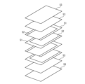
- FIG. 1 is a diagram illustrating a multilayer ceramic capacitor having a large number of layers.
- FIG. 13 is a diagram illustrating a debinder crack.
- 1A to 1C are diagrams illustrating a flow of a method for manufacturing a multilayer ceramic capacitor.
- FIG. 1 is a diagram illustrating a lamination process.
- FIG. 2 is a side view of a circuit board including a multilayer ceramic capacitor.
- FIG. 27 is a cross-sectional view of the package taken along line DD in FIG. 26.
- 11 is a diagram illustrating a crack at a corner portion near an external electrode.
- FIG. 13A to 13C are diagrams illustrating a multilayer ceramic capacitor according to a seventh embodiment.
- FIG. 13 is a diagram illustrating the dimension e.
- FIG. 1 is a diagram illustrating a lamination process.
- 13A to 13C are diagrams illustrating a multilayer ceramic capacitor according to an eighth embodiment.
- FIG. 1 is a diagram illustrating a
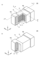
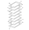
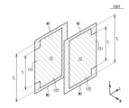
- First Embodiment 1(a) and 1(b) are partial cross-sectional perspective views of the multilayer ceramic capacitor 100 according to the first embodiment.
- FIG. 2 is a cross-sectional view taken along line A-A in FIG. 1(a).
- FIG. 3 is a cross-sectional view taken along line B-B in FIG. 1(a).
- the multilayer ceramic capacitor 100 includes a laminated chip 10 having a substantially rectangular parallelepiped shape, and external electrodes 20a and 20b provided on two opposing end faces of the laminated chip 10. Of the four faces of the laminated chip 10 other than the two end faces, the two faces at both ends in the lamination direction are referred to as the upper face and the lower face.
- the two faces other than the two end faces, the upper face, and the lower face are referred to as the side faces.
- the external electrodes 20a and 20b extend to the upper face, the lower face, and the two side faces in the lamination direction of the laminated chip 10. However, the external electrodes 20a and the external electrodes 20b are spaced apart from each other.
- the T direction (first direction) is the height direction of the multilayer ceramic capacitor 100, and is perpendicular to the direction in which the external electrodes 20a and 20b face each other (length direction: L direction).
- the W direction (second direction) is perpendicular to the T direction and the L direction.
- the T direction corresponds to the stacking direction of the internal electrode layers 12, and is the direction in which the upper and lower surfaces of the multilayer chip 10 face each other.
- the W direction is the direction in which the two side surfaces of the multilayer chip 10 face each other.
- the L direction is the direction in which the two end faces of the multilayer chip 10 face each other.
- the multilayer ceramic capacitor 100 in the T direction is defined as height T0
- the width of the multilayer ceramic capacitor 100 in the W direction is defined as width W0
- the length of the multilayer ceramic capacitor 100 in the L direction is defined as length L0
- the laminated chip 10 has a configuration in which dielectric layers 11 containing a ceramic material that functions as a dielectric and internal electrode layers 12 mainly composed of metal are alternately laminated.
- the laminated chip 10 has a plurality of internal electrode layers 12 facing each other and a dielectric layer 11 sandwiched between the plurality of internal electrode layers 12.
- the edges in the direction in which each internal electrode layer 12 extends are alternately exposed to the first end face on which the external electrode 20a of the laminated chip 10 is provided and the second end face on which the external electrode 20b is provided.
- the internal electrode layer 12 connected to the external electrode 20a is not connected to the external electrode 20b.
- the internal electrode layer 12 connected to the external electrode 20b is not connected to the external electrode 20a.
- each internal electrode layer 12 is alternately conductive to the external electrode 20a and the external electrode 20b.
- the internal electrode layer 12 is disposed on the top layer in the lamination direction, and the internal electrode layer 12 is also disposed on the bottom layer in the lamination direction, and both end faces in the lamination direction of the laminate are covered with a cover layer 13.
- the cover layer 13 is mainly composed of a ceramic material.
- the main component of the cover layer 13 is the same as the main component of the dielectric layer 11.
- the dielectric layer 11 has a main phase of a ceramic material having a perovskite structure represented by the general formula ABO 3.
- the perovskite structure includes ABO 3- ⁇ , which is not a stoichiometric composition.
- the ceramic material can be selected from at least one of BaTiO 3 (barium titanate), CaZrO 3 (calcium zirconate), CaTiO 3 (calcium titanate), SrTiO 3 (strontium titanate), MgTiO 3 (magnesium titanate), Ba 1-x-y Ca x Sr y Ti 1-z Zr z O 3 (0 ⁇ x ⁇ 1, 0 ⁇ y ⁇ 1, 0 ⁇ z ⁇ 1) that forms a perovskite structure, and the like.
- Ba1 -xyCaxSryTi1 - zZrzO3 is barium strontium titanate, barium calcium titanate, barium zirconate, barium zirconate titanate, calcium zirconate titanate and barium calcium zirconate titanate, etc.
- the dielectric layer 11 may contain additives.
- additives to the dielectric layer 11 include oxides of magnesium (Mg), manganese (Mn), molybdenum (Mo), vanadium (V), chromium (Cr), rare earth elements (yttrium (Y), samarium (Sm), europium (Eu), gadolinium (Gd), terbium (Tb), dysprosium (Dy), holmium (Ho), erbium (Er), thulium (Tm), and ytterbium (Yb)), or oxides containing cobalt (Co), nickel (Ni), lithium (Li), boron (B), sodium (Na), potassium (K), or silicon (Si), or glasses containing Co, Ni, Li, B, Na, K, or Si.
- each dielectric layer 11 in the stacking direction is, for example, 0.3 ⁇ m to 10 ⁇ m, or 0.4 ⁇ m to 8 ⁇ m, or 0.5 ⁇ m to 5 ⁇ m.
- the thickness of each dielectric layer 11 can be measured by exposing the cross section of the multilayer ceramic capacitor 100, for example, as shown in FIG. 2, by mechanical polishing, and then obtaining the average thickness value at 10 points from an image taken by a microscope such as a scanning transmission electron microscope.
- the internal electrode layer 12 is mainly composed of Ni.
- the thickness of each internal electrode layer 12 in the lamination direction is, for example, 0.1 ⁇ m or more and 2 ⁇ m or less.
- the thickness of each internal electrode layer 12 can be measured by exposing the cross section of the multilayer ceramic capacitor 100, for example, as shown in FIG. 2, by mechanical polishing, and then obtaining the average thickness value at 10 points from an image taken by a microscope such as a scanning transmission electron microscope.
- the region where the internal electrode layer 12 connected to the external electrode 20a and the internal electrode layer 12 connected to the external electrode 20b face each other is a region that generates capacitance in the multilayer ceramic capacitor 100. Therefore, this region that generates capacitance is referred to as the capacitance section 14.
- the capacitance section 14 is a region where adjacent internal electrode layers connected to different external electrodes face each other.
- the region where the internal electrode layers 12 connected to the external electrode 20a face each other without an internal electrode layer 12 connected to the external electrode 20b being interposed therebetween is called the end margin 15.
- the region where the internal electrode layers 12 connected to the external electrode 20b face each other without an internal electrode layer 12 connected to the external electrode 20a being interposed therebetween is also the end margin 15.
- the end margin is the region where the internal electrode layers connected to the same external electrode face each other without an internal electrode layer connected to a different external electrode being interposed therebetween.
- the end margin 15 is a region that does not generate capacitance.
- the end margin 15 may have the same composition as the dielectric layer 11 of the capacitance section 14, or may have a different composition.
- the areas extending from the two side surfaces to the internal electrode layer 12 are called side margins 16.
- the side margins 16 are also areas that do not generate capacitance.
- the side margins 16 may have the same composition as the dielectric layer 11 of the capacitance section 14, or may have a different composition.
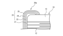
- the external electrode 20a has a structure in which a plating layer 22 is provided on a base layer 21, which is a contact layer in contact with the first end face of the laminated chip 10.
- the base layer 21 is mainly composed of Cu.
- the base layer 21 may also contain a glass component.
- the plating layer 22 is mainly composed of a metal such as Cu, Ni, aluminum (Al), zinc (Zn), Sn, etc., or an alloy of two or more of these.
- the plating layer 22 may be a plating layer of a single metal component, or may be a plurality of plating layers of different metal components.
- the plating layer 22 has a structure in which a first plating layer 23, a second plating layer 24, and a third plating layer 25 are formed in this order from the base layer 21 side.
- the first plating layer 23 is, for example, a Sn plating layer.
- the second plating layer 24 is, for example, a Ni plating layer.
- the third plating layer 25 is, for example, a Sn plating layer.
- the external electrode 20a is illustrated, but the external electrode 20b also has a similar laminated structure.
- the multilayer ceramic capacitor 100 according to this embodiment has a configuration that can suppress the occurrence of cracks due to Cu diffusion without excessively lowering the baking temperature.
- the internal electrode layer 12 and the underlayer 21 contain a low-melting-point metal that has a lower melting point than Cu, which is the main metal component of the underlayer 21.
- the low-melting-point metal is not particularly limited as long as it has a lower melting point than Cu, but examples of the low-melting-point metal include Ga (gallium), In (indium), Sn, Bi (bismuth), Zn, and Al.
- the low melting point metal may be alloyed with Ni, which is the main component of the internal electrode layer 12, or may be disposed as a single metal.
- the low melting point metal may be disposed in a uniformly dispersed manner in the internal electrode layer 12, or may be segregated at the interface between the internal electrode layer 12 and the dielectric layer 11.
- the low melting point metal may be alloyed with Cu, which is the main component of the underlayer 21, or may be disposed as a single metal.
- the low melting point metal may be disposed in a uniformly dispersed manner in the underlayer 21, or may be segregated at the interface between the underlayer 21 and the laminated chip 10.
- each internal electrode layer 12 in the in-plane direction has a first region 121 (connection portion) connected to the external electrode 20a in a region corresponding to the end margin 15 and having a dimension W1 in the W direction, and a second region 122 in a region corresponding to the capacitance portion 14 and having a dimension W2 in the W direction.
- the dimension W1 is smaller than the dimension W2.
- the first region 121 is located inside the second region 122.
- the internal electrode layer 12 connected to the external electrode 20b also has a first region 121 having a dimension W1 and a second region 122 having a dimension W2.
- the center of the first region 121 in the W direction coincides with the center of the second region 122 in the W direction.
- the underlayer 21 containing low melting point metals such as Ga, In, Sn, Bi, Zn, and Al is used to prevent deterioration of insulation resistance due to hydrogen generated in the plating process, or the internal electrode layer 12 containing low melting point metals such as Ga, In, Sn, Bi, Zn, and Al is used to change the potential barrier at the interface with the dielectric layer 11 and improve the high temperature load life, the movement distance from the underlayer 21 to the internal electrode layer 12 is long at the corners, so diffusion from the underlayer 21 to the internal electrode layer 12 is suppressed. This suppresses the occurrence of cracks 40. From the above, it is possible to suppress the occurrence of cracks without excessively lowering the baking temperature. As a result, the denseness of the underlayer 21 can be ensured.
- W1/W2 is small, the connectivity between the external electrodes 20a, 20b and the internal electrode layer 12 may decrease, and good electrical continuity may not be obtained. Therefore, it is preferable to set a lower limit for W1/W2.
- W1/W2 is large, the movement distance from the external electrodes 20a, 20b to the internal electrode layer 12 may not be sufficiently long. Therefore, it is preferable to set an upper limit for W1/W2.
- W1/W2 is preferably 1/2 or more, and more preferably 2/3 or more. Furthermore, W1/W2 is preferably 4/5 or less, and more preferably 3/4 or less.
- the dimension of the external electrodes 20a, 20b extending in the L direction from both end faces of the laminated chip 10 is referred to as dimension e.
- the dimension of the first region 121 in the L direction is 1/3 or more of dimension e, and more preferably 1/2 or more.
- the concentration of low melting point metal added is preferably 1 at% or more, more preferably 3 at% or more, and even more preferably 5 at% or more.
- the concentration of low melting point metal added refers to the amount of low melting point metal added (at%) when Cu is 100 at% in the entire underlayer 21.
- the concentration of low melting point metal added refers to the total amount of the multiple types of low melting point metals.
- the concentration of the low-melting-point metal added is preferably 20 at% or less, more preferably 15 at% or less, and even more preferably 10 at% or less.
- the concentration of the low melting point metal added is preferably 0.1 at% or more, more preferably 0.3 at% or more, and even more preferably 0.5 at% or more.
- the concentration of the low melting point metal added refers to the amount of low melting point metal added (at%) when Ni is 100 at% in the entire one internal electrode layer 12 between two adjacent dielectric layers 11.
- the concentration of the low melting point metal added refers to the total amount of the multiple types of low melting point metals.
- the concentration of the low-melting-point metal added is preferably 10 at% or less, more preferably 5 at% or less, and even more preferably 2 at% or less.
- the stacking density of the internal electrode layers 12 is, for example, 500 layers/mm or more, 750 layers/mm or more, or 1000 layers/mm or more and 1500 layers/mm or less.
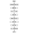
- Figure 8 is a diagram illustrating the flow of the method for manufacturing the multilayer ceramic capacitor 100.
- a dielectric material for forming the dielectric layer 11 is prepared.
- the A-site elements and B-site elements contained in the dielectric layer 11 are usually contained in the dielectric layer 11 in the form of a sintered body of ABO3 particles.
- BaTiO3 is a tetragonal compound having a perovskite structure and exhibits a high dielectric constant. This BaTiO3 can generally be obtained by reacting a titanium raw material such as titanium dioxide with a barium raw material such as barium carbonate to synthesize barium titanate.
- a predetermined additive compound is added to the obtained ceramic powder according to the purpose.
- the additive compound may be an oxide of Mg, Mn, Mo, V, Cr, or a rare earth element (Y, Sm, Eu, Gd, Tb, Dy, Ho, Er, Tm, or Yb), or an oxide containing Co, Ni, Li, B, Na, K, or Si, or a glass containing Co, Ni, Li, B, Na, K, or Si.
- SiO2 mainly functions as a sintering aid.
- a compound containing an additive compound is wet mixed with a ceramic raw material powder, and then dried and pulverized to prepare a ceramic material.
- the ceramic material obtained as described above may be pulverized as necessary to adjust the particle size, or may be combined with a classification process to adjust the particle size. Through the above steps, a dielectric material is obtained.
- a binder such as polyvinyl butyral (PVB) resin, an organic solvent such as ethanol or toluene, and a plasticizer are added to the obtained raw material powder and wet mixed.
- a dielectric green sheet is coated on a substrate by, for example, a die coater method or a doctor blade method, and then dried.
- the substrate is, for example, a polyethylene terephthalate (PET) film.
- an internal electrode pattern is formed on the dielectric green sheet.
- the dielectric green sheet on which the internal electrode pattern is formed is used as a lamination unit.
- Ni powder containing a low-melting point metal with a lower melting point than Cu is used for the internal electrode pattern.
- the film formation method may be printing, sputtering, vapor deposition, etc.
- the dielectric green sheet is peeled off from the substrate while stacking the lamination units.
- a predetermined number of cover sheets e.g., 2 to 10 layers
- the cover sheets can be formed using the same method as the dielectric green sheets.
- the laminate thus obtained is subjected to a binder removal treatment in a N2 atmosphere at a heat treatment temperature of about 250°C to 700°C.
- the laminated chip 10 is sintered in a reducing atmosphere with an oxygen partial pressure of 10 ⁇ 5 to 10 ⁇ 8 atm at 1100 to 1300° C. for 10 minutes to 2 hours.
- a re-oxidation treatment may be performed at 600° C. to 1000° C. in a N 2 gas atmosphere.
- a metal paste that will become the underlayer 21 is applied to the first side surface of the laminate by a dipping method or the like.
- This metal paste contains a glass component such as glass frit, and also contains a low-melting point metal that has a lower melting point than Cu.
- the metal paste is baked at a temperature of about 700° C. to 900° C. to form the underlayer 21 .
- a metal coating such as copper, nickel, or tin may be applied to the underlayer 21 by a plating process.
- the first plating layer 23, the second plating layer 24, and the third plating layer 25 are formed in this order on the underlayer 21. In this manner, the multilayer ceramic capacitor 100 is completed.
- the distance traveled from the base layer 21 to the internal electrode layer 12 is longer at the corners, suppressing diffusion from the base layer 21 to the internal electrode layer 12. This suppresses the occurrence of cracks 40. As a result, it is possible to suppress the occurrence of cracks without excessively lowering the baking temperature. As a result, it is possible to ensure the denseness of the base layer 21.
- the base layer 21 is baked after the laminated chip 10 is baked, but this is not limited to the above.
- the base layer 21 may be baked at the same time as the laminated chip 10 is baked.
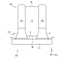
- FIG. 9 is a side view of a circuit board 200 including the multilayer ceramic capacitor 100.
- the circuit board 200 has a mounting board 210 on which the multilayer ceramic capacitor 100 is mounted.
- the mounting board 210 has a base material 211 that extends along a plane in the L direction and W direction and has a mounting surface G perpendicular to the T direction, and a pair of connection electrodes 212 provided on the mounting surface G.
- the external electrodes 20a, 20b of the multilayer ceramic capacitor 100 are each connected to a pair of connection electrodes 212 of the mounting board 210 via solder H.
- the multilayer ceramic capacitor 100 is fixed to and electrically connected to the mounting board 210.
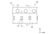
- the multilayer ceramic capacitor 100 is prepared in a packaged state as a package 300 when mounted on a mounting substrate 210.
- Figures 10 and 11 are diagrams illustrating an example of the package 300.
- Figure 10 is a partial plan view of the package 300.
- Figure 11 is a cross-sectional view of the package 300 taken along line C-C in Figure 10.
- the package 300 includes a multilayer ceramic capacitor 100, a carrier tape 310, and a top tape 320.
- the carrier tape 310 is configured as a long tape extending in the W direction.
- the carrier tape 310 has a plurality of recesses 311 arranged at intervals in the W direction, each of which accommodates one of the multilayer ceramic capacitors 100.
- the carrier tape 310 has a sealing surface P, which is an upward surface perpendicular to the T direction, and the multiple recesses 311 are recessed downward in the T direction from the sealing surface P.
- the carrier tape 310 is configured so that the multilayer ceramic capacitors 100 in the multiple recesses 311 can be removed from the sealing surface P side.
- the carrier tape 310 has a plurality of feed holes 312 arranged at intervals in the W direction and penetrating in the T direction at positions offset in the L direction from the row of the plurality of recesses 311.
- the feed holes 312 are configured as engagement holes used by the tape transport mechanism to transport the carrier tape 310 in the W direction.
- the top tape 320 is attached to the seal surface P of the carrier tape 310 along the row of the recesses 311, and the recesses 311 housing the multilayer ceramic capacitors 100 are collectively covered by the top tape 320. This allows the multilayer ceramic capacitors 100 to be held within the recesses 311.
- the first main surface M1 of the laminated chip 10 facing upward in the T direction faces the top tape 320.
- the second main surface M2 of the laminated chip 10 facing downward in the T direction faces the bottom surface of the recess 311.
- the top tape 320 is peeled off from the seal surface P of the carrier tape 310 along the W direction. This allows the package 300 to sequentially open the multiple recesses 311 housing the multiple multilayer ceramic capacitors 100 upward in the T direction.
- the multilayer ceramic capacitor 100 housed in the open recess 311 is removed with the first main surface M1 of the multilayer chip 10 facing upward in the T direction being adsorbed to the tip of the suction nozzle of the mounting device.
- the mounting device moves the suction nozzle to move the multilayer ceramic capacitor 100 onto the mounting surface G of the mounting board 210.
- the mounting device places the second main surface M2 of the laminated chip 10 opposite the mounting surface G, aligns the external electrodes 20a, 20b on the pair of connection electrodes 212 to which the solder paste has been applied, and releases the suction nozzle from suction onto the first main surface M1 of the laminated chip 10. This places the laminated ceramic capacitor 100 on the mounting surface G.
- the solder paste is melted and then hardened using a reflow oven or the like on the mounting board 210 on which the multilayer ceramic capacitor 100 is placed on the mounting surface G.
- the external electrodes 20a, 20b are connected to the pair of connection electrodes 212 of the mounting board 210 via the solder H, thereby obtaining the circuit board 200 shown in FIG. 9.
- Second Embodiment 12(a) and 12(b) are partial cross-sectional perspective views of the multilayer ceramic capacitor 100a according to the second embodiment.
- the multilayer ceramic capacitor 100a differs from the multilayer ceramic capacitor 100 according to the first embodiment in the ratio of T 0 /W 0 .
- T 0 /W 0 is 1.3 times or more.
- the number of stacked internal electrode layers 12 can be increased, and therefore the capacitance can be increased. From the viewpoint of increasing the capacitance, it is preferable that T 0 /W 0 is 1.5 times or more.
- Third Embodiment 13(a) and 13(b) are partial cross-sectional perspective views of a multilayer ceramic capacitor 100b according to the third embodiment.
- the multilayer ceramic capacitor 100b differs from the multilayer ceramic capacitor 100 according to the first embodiment in that not all of the internal electrode layers 12 have the first region 121 and the second region 122, but some of the internal electrode layers 12 have the first region 121 and the second region 122.
- one or more internal electrode layers 12 have the first region 121 and the second region 122 from the outermost internal electrode layer 12 toward the inside.
- the internal electrode layer 12 having the first region 121 and the second region 122 is referred to as the internal electrode layer 12 in the outer region.
- the internal electrode layer 12 that is located inside the internal electrode layer 12 in the outer region and has a substantially constant dimension in the W direction is referred to as the internal electrode layer 12 in the inner region.
- the internal electrode layers 12 that make up a total of 10% or more of the total number of layers are the internal electrode layers 12 in the outer region, and it is more preferable that the internal electrode layers 12 that make up 25% or more of the total number of layers are the internal electrode layers 12 in the outer region.
- the internal electrode layers 12 that make up a total of 50% or less of the total number of layers are the internal electrode layers 12 in the outer region, and it is more preferable that the internal electrode layers 12 that make up 40% or less of the total number of layers are the internal electrode layers 12 in the outer region.
- the number of layers of the internal electrode layers 12 in the outer region on one side of the internal electrode layers 12 in the inner region in the T direction is the same as the number of layers of the internal electrode layers 12 in the outer region on the other side of the T direction.
- the capacitance can be increased by increasing the number of stacked internal electrode layers 12.
- T 0 /W 0 is preferably 1.3 times or more, and more preferably 1.5 times or more.
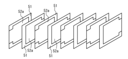
- the multilayer ceramic capacitor 100b according to this embodiment can be obtained, for example, by laminating a dielectric green sheet 51 on which an internal electrode pattern 52a having dimensions W1 and W2 is formed, and a dielectric green sheet 51 on which an internal electrode pattern 52 having a constant dimension in the W direction is formed, as illustrated in FIG. 14.
- Fourth Embodiment 15(a) and 15(b) are partial cross-sectional perspective views of a multilayer ceramic capacitor 100c according to the fourth embodiment.
- the multilayer ceramic capacitor 100c differs from the multilayer ceramic capacitor 100 according to the first embodiment in the lamination direction of the internal electrode layers 12.
- the W direction corresponds to the lamination direction of the internal electrode layers 12, and is the direction in which the upper and lower surfaces of the laminated chip 10 face each other.
- the T direction is the direction in which the two side surfaces of the laminated chip 10 face each other.
- the L direction is the direction in which the two end surfaces of the laminated chip 10 face each other. Therefore, in this embodiment, the dimension W1 in the first embodiment can be read as the dimension T1 in the T direction, and the dimension W2 can be read as the dimension T2 in the T direction.
- the multilayer ceramic capacitor 100c When the multilayer ceramic capacitor 100c is mounted on the mounting substrate 210, one of the two sides of the multilayer ceramic capacitor 100c faces the mounting substrate 210.
- circuit board 200 repeated electrostriction occurs in the multilayer ceramic capacitor 100c when an AC voltage is applied, which can cause vibrations in the thickness direction of the substrate 211 of the mounting board 210.
- vibrations generated in the substrate 211 become large, noise can be generated from the substrate 211, which is a phenomenon known as "ringing.”
- the lamination direction of the internal electrode layers 12 is the in-plane direction of the substrate 211, so that electrostriction of the laminated chip 10 is unlikely to cause vibration in the thickness direction of the substrate 211.
- the number of layers of the internal electrode layers 12 is small, and the amount of deformation due to electrostriction is kept small, so that even if vibration does occur in the substrate 211, it is unlikely to be large enough to cause noise.
- the multilayer ceramic capacitor 100d is different from the multilayer ceramic capacitor 100c according to the fourth embodiment in that not all of the internal electrode layers 12 have the first region 121 and the second region 122, but some of the internal electrode layers 12 have the first region 121 and the second region 122.
- one or more internal electrode layers 12 have the first region 121 and the second region 122 from the outermost internal electrode layer 12 toward the inside.
- the internal electrode layer 12 having the first region 121 and the second region 122 is referred to as the internal electrode layer 12 in the outer region.
- the internal electrode layer 12 that is located inside the internal electrode layer 12 in the outer region and has a substantially constant dimension in the T direction is referred to as the internal electrode layer 12 in the inner region.
- the internal electrode layers 12 that make up a total of 10% or more of the total number of layers are the internal electrode layers 12 in the outer region, and it is more preferable that the internal electrode layers 12 that make up 25% or more of the total number of layers are the internal electrode layers 12 in the outer region.
- the internal electrode layers 12 that make up a total of 50% or less of the total number of layers are the internal electrode layers 12 in the outer region, and it is more preferable that the internal electrode layers 12 that make up 40% or less of the total number of layers are the internal electrode layers 12 in the outer region.
- the number of layers of the internal electrode layers 12 in the outer region on one side in the W direction from the internal electrode layers 12 in the inner region is the same as the number of layers of the internal electrode layers 12 in the outer region on the other side in the W direction.
- the multilayer ceramic capacitor 100d When the multilayer ceramic capacitor 100d is mounted on the mounting substrate 210, one of the two sides of the multilayer ceramic capacitor 100d faces the mounting substrate 210.
- the circuit board 200 when the circuit board 200 is driven and a voltage is applied to the external electrodes 20a, 20b via the connection electrodes 212 of the mounting board 210, it is known that electrostriction occurs in the laminated chip 10 due to the piezoelectric effect.
- the electrostriction occurring in the laminated chip 10 causes a relatively large deformation in the lamination direction of the internal electrode layers 12.
- circuit board 200 repeated electrostriction occurs in the multilayer ceramic capacitor 100d when an AC voltage is applied, which can cause vibrations in the thickness direction of the substrate 211 of the mounting board 210.
- vibrations generated in the substrate 211 become large, noise can be generated from the substrate 211, which is a phenomenon known as "ringing.”
- the lamination direction of the internal electrode layers 12 is the in-plane direction of the substrate 211, so that electrostriction of the laminated chip 10 is unlikely to cause vibration in the thickness direction of the substrate 211.
- the number of layers of the internal electrode layers 12 is small, and the amount of deformation due to electrostriction is kept small, so that even if vibration does occur in the substrate 211, it is unlikely to be large enough to cause noise.
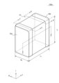
- FIG. 17 is an external view of the multilayer ceramic capacitor 100e according to the sixth embodiment.
- FIG. 18 is a cross-sectional view taken along line A-A in FIG. 17.
- FIG. 19 is a cross-sectional view taken along line B-B in FIG. 17.
- the multilayer ceramic capacitor 100e includes a laminated chip 10 having a substantially rectangular parallelepiped shape, and external electrodes 20a, 20b provided on two opposing end faces of the laminated chip 10. Of the four faces of the laminated chip 10 other than the two end faces, the two faces at both ends in the lamination direction are referred to as side faces.
- the two faces other than the two end faces and the two side faces are referred to as the upper face and the lower face.
- the lower face functions as a mounting face and faces the mounting substrate when the multilayer ceramic capacitor 100e is mounted on the mounting substrate.
- the external electrodes 20a, 20b extend to the upper face, the lower face, and the two side faces of the laminated chip 10. However, the external electrodes 20a and the external electrodes 20b are spaced apart from each other.
- the T direction (first direction) is the height direction of the multilayer ceramic capacitor 100e, and is the direction in which the upper and lower surfaces of the laminated chip 10 face each other.
- the W direction (second direction) is the stacking direction of the dielectric layers 11 and the internal electrode layers 12.
- the L direction (third direction) is the direction in which the two end faces of the laminated chip 10 face each other, and is the direction in which the external electrodes 20a and 20b face each other.
- the L direction, W direction, and T direction are mutually perpendicular.
- the laminated chip 10 has a configuration in which dielectric layers 11 containing a ceramic material that functions as a dielectric and internal electrode layers 12 mainly composed of metal are alternately laminated.
- the laminated chip 10 has a plurality of internal electrode layers 12 facing each other and a dielectric layer 11 sandwiched between the plurality of internal electrode layers 12.
- the edges in the direction in which each internal electrode layer 12 extends are alternately exposed to the first end face on which the external electrode 20a of the laminated chip 10 is provided and the second end face on which the external electrode 20b is provided.
- the internal electrode layer 12 connected to the external electrode 20a is not connected to the external electrode 20b.
- the internal electrode layer 12 connected to the external electrode 20b is not connected to the external electrode 20a.
- each internal electrode layer 12 is alternately conductive to the external electrode 20a and the external electrode 20b.
- the internal electrode layer 12 is disposed on the top layer in the lamination direction, and the internal electrode layer 12 is also disposed on the bottom layer in the lamination direction, and each of the two side surfaces of the laminate is covered with a cover layer 13.
- the cover layer 13 is mainly composed of a ceramic material.
- the main component of the cover layer 13 is the same as the main component of the dielectric layer 11.
- the dielectric layer 11 has a main phase of a ceramic material having a perovskite structure represented by the general formula ABO 3.
- the perovskite structure includes ABO 3- ⁇ , which is not a stoichiometric composition.
- the ceramic material can be selected from at least one of BaTiO 3 (barium titanate), CaZrO 3 (calcium zirconate), CaTiO 3 (calcium titanate), SrTiO 3 (strontium titanate), MgTiO 3 (magnesium titanate), Ba 1-x-y Ca x Sr y Ti 1-z Zr z O 3 (0 ⁇ x ⁇ 1, 0 ⁇ y ⁇ 1, 0 ⁇ z ⁇ 1) that forms a perovskite structure, and the like.
- Ba1 -xyCaxSryTi1 - zZrzO3 is barium strontium titanate, barium calcium titanate, barium zirconate, barium zirconate titanate, calcium zirconate titanate and barium calcium zirconate titanate, etc.
- the dielectric layer 11 may contain additives.
- additives to the dielectric layer 11 include oxides of magnesium (Mg), manganese (Mn), molybdenum (Mo), vanadium (V), chromium (Cr), rare earth elements (yttrium (Y), samarium (Sm), europium (Eu), gadolinium (Gd), terbium (Tb), dysprosium (Dy), holmium (Ho), erbium (Er), thulium (Tm), and ytterbium (Yb)), or oxides containing cobalt (Co), nickel (Ni), lithium (Li), boron (B), sodium (Na), potassium (K), or silicon (Si), or glasses containing Co, Ni, Li, B, Na, K, or Si.
- each dielectric layer 11 in the T direction is, for example, 0.3 ⁇ m or more and 3 ⁇ m or less.
- the thickness of each dielectric layer 11 in the T direction can be measured by exposing the cross section of the multilayer ceramic capacitor 100e, for example, as shown in FIG. 18, by mechanical polishing, and then obtaining the average thickness value at 10 points from an image taken by a microscope such as a scanning transmission electron microscope.
- the internal electrode layer 12 is mainly composed of Ni.
- the thickness of each internal electrode layer 12 in the T direction is, for example, 0.1 ⁇ m or more and 2 ⁇ m or less.
- the thickness of each internal electrode layer 12 in the T direction can be measured by exposing the cross section of the multilayer ceramic capacitor 100e, for example, as shown in FIG. 18, by mechanical polishing, and then obtaining the average thickness value at 10 points from an image taken by a microscope such as a scanning transmission electron microscope.
- the region where the internal electrode layer 12 connected to the external electrode 20a and the internal electrode layer 12 connected to the external electrode 20b face each other is a region that generates capacitance in the multilayer ceramic capacitor 100e. Therefore, this region that generates capacitance is referred to as the capacitance section 14.
- the capacitance section 14 is a region where adjacent internal electrode layers connected to different external electrodes face each other.
- the region where the internal electrode layers 12 connected to the external electrode 20a face each other without an internal electrode layer 12 connected to the external electrode 20b being interposed therebetween is called the end margin 15.
- the region where the internal electrode layers 12 connected to the external electrode 20b face each other without an internal electrode layer 12 connected to the external electrode 20a being interposed therebetween is also the end margin 15.
- the end margin is the region where the internal electrode layers connected to the same external electrode face each other without an internal electrode layer connected to a different external electrode being interposed therebetween.
- the end margin 15 is a region that does not generate capacitance.
- the end margin 15 may have the same composition as the dielectric layer 11 of the capacitance section 14, or may have a different composition.
- the region extending from the upper surface to the internal electrode layer 12 in the T direction and the region extending from the lower surface to the internal electrode layer 12 in the T direction are referred to as the side margin 16.
- the side margin 16 is a region provided to cover the ends of the multiple internal electrode layers 12 stacked in the laminated structure that extend to the upper and lower surfaces.
- the side margin 16 is also a region that does not generate capacitance.
- the side margin 16 may have the same composition as the dielectric layer 11 of the capacitance section 14, or a different composition.
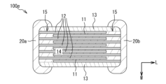
- the external electrode 20a is an enlarged cross-sectional view of the vicinity of the external electrode 20a. Hatching is omitted in FIG. 20.
- the external electrode 20a has a structure in which a plating layer 22 is provided on an underlayer 21.
- the underlayer 21 is mainly composed of Cu.
- the underlayer 21 may also contain a glass component.
- the plating layer 22 is mainly composed of a metal such as Ni, aluminum (Al), zinc (Zn), Sn, or an alloy of two or more of these.
- the plating layer 22 may be a plating layer of a single metal component, or may be a plurality of plating layers of different metal components.
- the plating layer 22 has a structure in which a first plating layer 23, a second plating layer 24, and a third plating layer 25 are formed in this order from the underlayer 21 side.
- the first plating layer 23 is, for example, a Sn plating layer.
- the second plating layer 24 is, for example, a Ni plating layer.
- the third plating layer 25 is, for example, a Sn plating layer. Note that while FIG. 20 illustrates the external electrode 20a, the external electrode 20b also has a similar layered structure.
- Increasing the total opposing area of the internal electrode layers is important when trying to realize a large-capacity multilayer ceramic capacitor.
- the total opposing area of the internal electrode layers 12 increases, which is thought to enable the realization of a large capacity.
- misalignment is more likely to occur during stacking, and it becomes difficult to cut the pre-fired laminate perpendicular to the stacking direction.
- the multilayer ceramic capacitor 100e has a configuration in which the area of each internal electrode layer is increased and the number of layers is reduced. Specifically, as illustrated in FIG. 17, when the height of the multilayer ceramic capacitor 100e in the T direction is height T0 , the width in the W direction is width W0 , and the length in the L direction is length L0 , the multilayer ceramic capacitor 100e has a relationship of T0 ⁇ W0 ⁇ 1.3. With this configuration, the width of the internal electrode layers 12 can be increased while the number of layers of the internal electrode layers 12 can be reduced, so that positional deviation during stacking can be suppressed and the pre-fired laminate can be cut perpendicular to the stacking direction. Note that the height T0 , width W0 , and length L0 are the maximum dimensions in the T direction, W direction, and L direction, respectively.
- the binder may not be sufficiently removed because the binder discharge path becomes long.
- the decomposition gas of the binder may remain inside the laminate, which may cause cracks (de-by-cracks) or delamination.
- the multilayer ceramic capacitor 100e according to this embodiment has a configuration that can achieve good binder removal properties even in a configuration in which the relationship T 0 ⁇ W 0 ⁇ 1.3 is established.
- a low-melting-point metal with a lower melting point than Cu, the main component of the underlayer 21, is provided inside the internal electrode layer 12 or at the interface between the internal electrode layer 12 and the dielectric layer 11.
- the low-melting-point metal is not particularly limited as long as it has a melting point lower than Cu, but examples include Ga (gallium), In (indium), Sn, Bi (bismuth), Pb (lead), and Zn.
- the low-melting-point metal may be alloyed with Ni, the main component of the internal electrode layer 12, or may be disposed as a single metal.
- the low-melting-point metal may be disposed uniformly dispersed in the internal electrode layer 12, or may be segregated at the interface between the internal electrode layer 12 and the dielectric layer 11.
- the binder ejection start temperature is lower during the heat treatment in the binder removal process compared to when the low melting point metal is not provided. This achieves good binder removal properties and makes it possible to suppress cracks and delamination.
- the binder ejection start temperature is lower because the low melting point metal melts at the binder ejection temperature, thereby making it easier to eject the binder.
- the concentration of the low melting point metal is preferably 0.1 at% or more, more preferably 0.3 at% or more, and even more preferably 0.5 at% or more.
- the concentration of the low melting point metal refers to the amount of low melting point metal added (at%) in the entire one internal electrode layer 12 sandwiched between two adjacent dielectric layers, when the Ni of the internal electrode layer 12 is 100 at%.
- the concentration of the low melting point metal refers to the total amount of the multiple types of low melting point metals.
- the concentration of the low-melting metal added is preferably 10 at% or less, more preferably 5 at% or less, and even more preferably 2 at% or less.
- the height T0 , width W0 , and length L0 are not particularly limited, but for example, the height T0 can be 0.15 mm or more and 1.0 mm or less, the width W0 can be 0.1 mm or more and 0.7 mm or less, and the length L0 can be 0.2 mm or more and 1.2 mm or less.
- the stacking density of the internal electrode layers 12 is, for example, 500 layers/mm or more, 750 layers/mm or more, or 1000 layers/mm or more and 1500 layers/mm or less.
- T 0 is preferably 1.5 times or more, and more preferably 2.0 times or more, of W 0 .
- T a is 500 times or more, 700 times or more, or 1000 times or more of W a .
- W ratio is, for example, 1.3 times or more, 1.5 times or more, or 2.0 times or more.
- Figure 23 is a diagram illustrating the flow of the method for manufacturing the multilayer ceramic capacitor 100e.
- a dielectric material for forming the dielectric layer 11 is prepared.
- the A-site elements and B-site elements contained in the dielectric layer 11 are usually contained in the dielectric layer 11 in the form of a sintered body of ABO3 particles.
- BaTiO3 is a tetragonal compound having a perovskite structure and exhibits a high dielectric constant. This BaTiO3 can generally be obtained by reacting a titanium raw material such as titanium dioxide with a barium raw material such as barium carbonate to synthesize barium titanate.
- a predetermined additive compound is added to the obtained ceramic powder according to the purpose.
- the additive compound may be an oxide of Mg, Mn, Mo, V, Cr, or a rare earth element (Y, Sm, Eu, Gd, Tb, Dy, Ho, Er, Tm, or Yb), or an oxide containing Co, Ni, Li, B, Na, K, or Si, or a glass containing Co, Ni, Li, B, Na, K, or Si.
- SiO2 mainly functions as a sintering aid.
- a compound containing an additive compound is wet mixed with a ceramic raw material powder, and then dried and pulverized to prepare a ceramic material.
- the ceramic material obtained as described above may be pulverized as necessary to adjust the particle size, or may be combined with a classification process to adjust the particle size. Through the above steps, a dielectric material is obtained.
- a binder such as polyvinyl butyral (PVB) resin, an organic solvent such as ethanol or toluene, and a plasticizer are added to the obtained raw material powder and wet mixed.
- a dielectric green sheet is coated on a substrate by, for example, a die coater method or a doctor blade method, and then dried.
- the substrate is, for example, a polyethylene terephthalate (PET) film.
- an internal electrode pattern 52 is formed on a dielectric green sheet 51.
- the dielectric green sheet 51 on which the internal electrode pattern 52 is formed is used as a lamination unit.
- Ni powder containing a low-melting point metal with a lower melting point than Cu is used for the internal electrode pattern 52.
- the film formation method may be printing, sputtering, vapor deposition, etc.
- cover sheets 53 e.g., 2 to 10 layers are stacked on top and bottom of the laminate obtained by stacking the lamination units, and are thermocompression bonded.
- the cover sheets 53 can be formed by the same method as the dielectric green sheet 51.
- the laminate thus obtained is subjected to a debindering treatment in a N2 atmosphere at a heat treatment temperature of about 250° C. to 700° C. for a heat treatment time of about 5 minutes to 1 hour.
- the laminated chip 10 is sintered in a reducing atmosphere with an oxygen partial pressure of 10 ⁇ 5 to 10 ⁇ 8 atm at 1100° C. to 1300° C. for 10 minutes to 2 hours.
- a re-oxidation treatment may be performed at 600° C. to 1000° C. in a N 2 gas atmosphere.
- a metal paste that will become the underlayer 21 is applied to the first side surface of the laminate by a dipping method or the like.
- This metal paste contains a glass component such as glass frit.
- the metal paste is baked at a temperature of about 700° C. to 900° C. to form the underlayer 21 .
- a metal coating such as copper, nickel, or tin may be applied to the underlayer 21 by a plating process.
- the first plating layer 23, the second plating layer 24, and the third plating layer 25 are formed in this order on the underlayer 21. This completes the multilayer ceramic capacitor 100e.
- a low melting point metal is added to the internal electrode pattern 52.
- the binder ejection start temperature during the heat treatment in the binder removal process becomes lower than when the low melting point metal is not added. This achieves good binder removal characteristics and makes it possible to suppress cracks and delamination.
- the base layer 21 is baked after the laminated chip 10 is baked, but this is not limited to the above.
- the base layer 21 may be baked at the same time as the laminated chip 10 is baked.
- FIG 25 is a side view of a circuit board 200 including the multilayer ceramic capacitor 100e.
- the circuit board 200 has a mounting board 210 on which the multilayer ceramic capacitor 100e is mounted.
- the mounting board 210 has a base material 211 that extends along a plane in the L direction and W direction and has a mounting surface G perpendicular to the T direction, and a pair of connection electrodes 212 provided on the mounting surface G.
- the external electrodes 20a, 20b of the multilayer ceramic capacitor 100e are each connected to a pair of connection electrodes 212 of the mounting board 210 via solder H.
- the multilayer ceramic capacitor 100e is fixed to and electrically connected to the mounting board 210.
- circuit board 200 repeated electrostriction occurs in the multilayer ceramic capacitor 100e when an AC voltage is applied, which can cause vibrations in the thickness direction of the substrate 211 of the mounting board 210.
- vibrations generated in the substrate 211 become large, noise can be generated from the substrate 211, which is a phenomenon known as "ringing.”
- the lamination direction of the internal electrode layers 12 is the in-plane direction of the substrate 211, so that electrostriction of the laminated chip 10 is unlikely to cause vibration in the thickness direction of the substrate 211.
- the number of layers of the internal electrode layers 12 is small, and the amount of deformation due to electrostriction is kept small, so that even if vibration does occur in the substrate 211, it is unlikely to be large enough to cause noise.
- the multilayer ceramic capacitor 100e is prepared in a packaged state as a package 300 when mounted on the mounting substrate 210.
- Figures 26 and 27 are diagrams illustrating the package 300.
- Figure 26 is a partial plan view of the package 300.
- Figure 27 is a cross-sectional view of the package 300 taken along line D-D in Figure 26.
- the package 300 includes a multilayer ceramic capacitor 100e, a carrier tape 310, and a top tape 320.
- the carrier tape 310 is configured as a long tape extending in the W direction.
- the carrier tape 310 has a plurality of recesses 311 arranged at intervals in the W direction, each of which accommodates one of the multilayer ceramic capacitors 100e.
- the carrier tape 310 has a sealing surface P, which is an upward surface perpendicular to the T direction, and the multiple recesses 311 are recessed downward in the T direction from the sealing surface P.
- the carrier tape 310 is configured so that the multilayer ceramic capacitors 100e in the multiple recesses 311 can be removed from the sealing surface P side.
- the carrier tape 310 has a plurality of feed holes 312 arranged at intervals in the W direction and penetrating in the T direction at positions offset in the L direction from the row of the plurality of recesses 311.
- the feed holes 312 are configured as engagement holes used by the tape transport mechanism to transport the carrier tape 310 in the W direction.
- the top tape 320 is attached to the seal surface P of the carrier tape 310 along the row of the recesses 311, and the recesses 311 housing the multilayer ceramic capacitors 100e are collectively covered by the top tape 320. This allows the multilayer ceramic capacitors 100e to be held within the recesses 311.
- the first main surface M1 of the laminated chip 10 facing upward in the T direction faces the top tape 320.
- the second main surface M2 of the laminated chip 10 facing downward in the T direction faces the bottom surface of the recess 311.
- the top tape 320 is peeled off from the seal surface P of the carrier tape 310 along the W direction. This allows the package 300 to sequentially open the multiple recesses 311 housing the multiple multilayer ceramic capacitors 100e upward in the T direction.
- the multilayer ceramic capacitor 100e housed in the opened recess 311 is removed with the first main surface M1 of the multilayer chip 10 facing upward in the T direction being adsorbed to the tip of the suction nozzle of the mounting device.
- the mounting device moves the suction nozzle to move the multilayer ceramic capacitor 100e onto the mounting surface G of the mounting board 210.
- the mounting device places the second main surface M2 of the laminated chip 10 facing the mounting surface G, aligns the external electrodes 20a, 20b on the pair of connection electrodes 212 to which the solder paste has been applied, and releases the suction nozzle from suctioning the first main surface M1 of the laminated chip 10. This places the laminated ceramic capacitor 100e on the mounting surface G.
- the solder paste is melted and then hardened using a reflow oven or the like on the mounting board 210 on which the multilayer ceramic capacitor 100e is placed on the mounting surface G.
- the external electrodes 20a, 20b are connected to the pair of connection electrodes 212 of the mounting board 210 via the solder H, and the circuit board 200 shown in FIG. 25 is obtained.
- Fig. 28 is a view corresponding to the cross section along the line CC in Fig. 17.
- the dimensions of each internal electrode layer 12 in the T direction are varied.
- the internal electrode layer 12 connected to the external electrode 20a has a first region 121 (connection portion) connected to the external electrode 20a in a region corresponding to the end margin 15 and having a dimension T1 in the T direction, and a second region 122 having a dimension T2 in the T direction in a region corresponding to the capacitance portion 14.
- the dimension T1 is lower than the dimension T2.
- the first region 121 is located inside the second region 122.
- the internal electrode layer 12 connected to the external electrode 20b also has a first region 121 having a dimension T1 and a second region 122 having a dimension T2.
- T1/T2 is preferably 1/2 or more, and more preferably 2/3 or more. Furthermore, T1/T2 is preferably 4/5 or less, and more preferably 3/4 or less.
- the dimension of the external electrodes 20a, 20b extending in the L direction from both end faces of the laminated chip 10 is referred to as dimension e.
- the dimension of the first region 121 in the L direction is 1/3 or more of dimension e, and more preferably 1/2 or more.
- the multilayer ceramic capacitor 100f according to this embodiment can be obtained, for example, by stacking dielectric green sheets 51 on which internal electrode patterns 52a having dimensions T1 and T2 are formed, as illustrated in FIG. 31.
- all the internal electrode layers 12 have the first region 121 and the second region 122, but some of the internal electrode layers 12 may have the first region 121 and the second region 122.
- the internal electrode layer 12 having the first region 121 and the second region 122 is referred to as the internal electrode layer 12 in the outer region.
- the internal electrode layer 12 that is located inside the internal electrode layer 12 in the outer region and has a substantially constant height in the T direction is referred to as the internal electrode layer 12 in the inner region.
- the internal electrode layers 12 that make up a total of 10% or more of the total number of layers are the internal electrode layers 12 in the outer region, and it is more preferable that the internal electrode layers 12 that make up 25% or more of the total number of layers are the internal electrode layers 12 in the outer region.
- the internal electrode layers 12 that make up a total of 50% or less of the total number of layers are the internal electrode layers 12 in the outer region, and it is more preferable that the internal electrode layers 12 that make up 40% or less of the total number of layers are the internal electrode layers 12 in the outer region.
- the number of layers of the internal electrode layers 12 in the outer region on one side in the W direction from the internal electrode layers 12 in the inner region is the same as the number of layers of the internal electrode layers 12 in the outer region on the other side in the W direction.
- the multilayer ceramic capacitor 100g according to this embodiment can be obtained, for example, by laminating a dielectric green sheet 51 on which an internal electrode pattern 52a having dimensions T1 and T2 is formed, and a dielectric green sheet 51 on which an internal electrode pattern 52 having a constant dimension in the T direction is formed, as illustrated in FIG. 33.
- a multilayer ceramic capacitor has been described as an example of a ceramic electronic component, but the present invention is not limited to this.
- the configuration of each of the above embodiments can also be applied to other multilayer ceramic electronic components, such as varistors and thermistors.
- the multilayer ceramic capacitors according to each embodiment were fabricated and their characteristics were investigated.
- Example 1 the multilayer ceramic capacitor described in the first embodiment was produced. First, a slurry mainly composed of BaTiO3 was mixed and coated to obtain a dielectric green sheet. An internal electrode pattern was printed on each dielectric green sheet. Nickel powder was used for the internal electrode pattern, and Sn powder was added. The concentration of Sn added to Ni was 1.0 at%. 250 layers of the obtained laminate unit were laminated to obtain a laminate.
- a slurry mainly composed of BaTiO 3 was mixed and applied to obtain a cover sheet.
- a plurality of cover sheets were laminated and pressed on the top and bottom of the laminate in the lamination direction, and then a binder removal process was performed. Then, the laminate was fired and reoxidized.
- a metal paste mainly composed of Cu was applied to two end faces of the obtained laminated chip and baked at about 800°C. Through these processes, a multilayer ceramic capacitor was produced in which 250 internal electrode layers were laminated, with a length L 0 of 0.6 mm, a width W 0 of 0.3 mm, and a height T 0 of 0.3 mm.
- each internal electrode layer in the T direction was 0.5 ⁇ m, and the thickness of each dielectric layer in the T direction was 0.5 ⁇ m.
- the thickness of each cover layer in the T direction was 25 ⁇ m.
- the thickness of each side margin in the W direction was 25 ⁇ m.
- the dimension W2 in the W direction was made larger in the capacitive section, and the dimension W1 in the W direction in the end margin was made smaller than W2.
- the dimension W2 of the internal electrode layer in the capacitive section was 250 ⁇ m, and the dimension W1 of the internal electrode layer in the end margin was 150 ⁇ m.
- the length in the L direction of each end margin was 15 ⁇ m.
- the dimension e of each external electrode extending in the L direction from both end faces of the multilayer chip was 20 ⁇ m.
- Example 2-1 the multilayer ceramic capacitor described in the second embodiment was produced.
- the number of stacked internal electrode layers was 350.
- the length L0 was 0.6 mm
- the width W0 was 0.3 mm
- the height T0 was 0.4 mm.
- the other conditions were the same as those in Example 1.
- Example 2-2 the multilayer ceramic capacitor described in the second embodiment was produced.
- the number of stacked internal electrode layers was 450.
- the length L0 was 0.6 mm
- the width W0 was 0.3 mm
- the height T0 was 0.5 mm.
- the other conditions were the same as those of Example 1.
- Example 3 In Example 3, the multilayer ceramic capacitor described in the third embodiment was fabricated.
- the number of layers of the internal electrode layers was 450.
- the length L 0 was 0.6 mm
- the width W 0 was 0.3 mm
- the height T 0 was 0.5 mm.
- the dimension W2 in the W direction was made larger in the capacitance section
- the dimension W1 in the W direction was made smaller than W2 in the end margin.
- the dimension W2 of the internal electrode layer in the capacitance section was 250 ⁇ m
- the dimension W1 of the internal electrode layer in the end margin was 150 ⁇ m.
- the dimension in the W direction of the internal electrode layer in the capacitance section and the dimension in the W direction of the internal electrode layer in the end margin were 250 ⁇ m.
- Other conditions were the same as in Example 1.
- Example 4-1 In Example 4-1, the multilayer ceramic capacitor described in the fourth embodiment was fabricated.
- the number of layers of the internal electrode layers was 250.
- the length L 0 was 0.6 mm
- the width W 0 was 0.3 mm
- the height T 0 was 0.5 mm.
- the thickness of each internal electrode layer in the W direction was 0.5 ⁇ m
- the thickness of each dielectric layer in the W direction was 0.5 ⁇ m.
- the thickness of each cover layer in the W direction was 25 ⁇ m.
- the thickness of each side margin in the T direction was 25 ⁇ m.
- the dimension T2 in the T direction was made larger in the capacitance section
- the dimension T1 in the T direction was made smaller than T2 in the end margin.
- the dimension T2 of the internal electrode layer in the capacitance section was 450 ⁇ m, and the dimension T1 of the internal electrode layer in the end margin was 300 ⁇ m.
- the length of each end margin in the L direction was 15 ⁇ m.
- the dimension e of each external electrode extending in the L direction from both end faces of the laminated chip was 20 ⁇ m.
- Example 4-2 In Example 4-2, the multilayer ceramic capacitor described in the fourth embodiment was fabricated.
- the number of layers of the internal electrode layers was 250.
- the length L 0 was 0.6 mm
- the width W 0 was 0.3 mm
- the height T 0 was 0.4 mm.
- the thickness of each internal electrode layer in the W direction was 0.5 ⁇ m
- the thickness of each dielectric layer in the W direction was 0.5 ⁇ m.
- the thickness of each cover layer in the W direction was 25 ⁇ m.
- the thickness of each side margin in the T direction was 25 ⁇ m.
- the dimension T2 in the T direction was made larger in the capacitance section
- the dimension T1 in the T direction was made smaller than T2 in the end margin.
- the dimension T2 of the internal electrode layer in the capacitance section was 350 ⁇ m, and the dimension T1 of the internal electrode layer in the end margin was 250 ⁇ m.
- the length of each end margin in the L direction was 15 ⁇ m.
- the dimension e of each external electrode extending in the L direction from both end faces of the laminated chip was 20 ⁇ m.
- Example 5 the multilayer ceramic capacitor described in the fifth embodiment was produced.
- the dimension T2 in the T direction was made larger in the capacitive section, and the dimension T1 in the T direction was made smaller than T2 in the end margin.
- the dimension T2 of the internal electrode layer in the capacitive section was 450 ⁇ m, and the dimension T1 of the internal electrode layer in the end margin was 300 ⁇ m.
- the dimension in the T direction of the internal electrode layer in the capacitive section and the dimension in the T direction of the internal electrode layer in the end margin were 450 ⁇ m.
- Other conditions were the same as in Example 4.
- Table 1 shows the conditions for Examples 1 to 5 and Comparative Examples 1 and 2.
- Example 6 the multilayer ceramic capacitor described in the sixth embodiment was produced.
- a slurry mainly composed of BaTiO3 was mixed and coated to obtain a dielectric green sheet.
- An internal electrode pattern was printed on each dielectric green sheet.
- Nickel powder was used for the internal electrode pattern, and Sn powder was added.
- the concentration of Sn added to Ni was 1.0 at%.
- the height of each internal electrode pattern was made lower than the height of the dielectric green sheet. 250 layers of the obtained laminate unit were laminated to obtain a laminate.
- a slurry mainly composed of BaTiO 3 was mixed and applied to obtain a cover sheet.
- a plurality of cover sheets were laminated and pressed on the top and bottom of the laminate in the lamination direction, and then barrel polishing and a binder removal process were performed. Then, the laminate was fired and reoxidized.
- a metal paste mainly composed of Cu was applied to two end faces of the obtained laminated chip and baked at about 800 ° C. Through these processes, a multilayer ceramic capacitor was produced in which the internal electrode layers were laminated in 250 layers, with a length L 0 of 0.6 mm, a width W 0 of 0.3 mm, and a height T 0 of 0.5 mm.
- each internal electrode layer in the W direction was 0.5 ⁇ m
- the thickness of each dielectric layer in the W direction was 0.5 ⁇ m
- the thickness of each cover layer in the W direction was 25 ⁇ m.
- the thickness of each side margin in the T direction was 25 ⁇ m.
- the length of each end margin in the L direction was 40 ⁇ m.
- Example 7 In Example 7, the multilayer ceramic capacitor described in the seventh embodiment was fabricated. In each internal electrode layer, the dimension T2 in the T direction was made larger in the capacitance section, and the dimension T1 in the T direction was made smaller than T2 in the end margin. The dimension T2 of the internal electrode layer in the capacitance section was 450 ⁇ m, and the dimension T1 of the internal electrode layer in the end margin was 300 ⁇ m. The other conditions were the same as in Example 6.
- Example 8 In Example 8, the multilayer ceramic capacitor described in the eighth embodiment was fabricated. In each of the 50 internal electrode layers in the outer region, the dimension T2 in the T direction was made larger in the capacitive portion, and the dimension T1 in the T direction was made smaller than T2 in the end margin. The dimension T2 of the internal electrode layer in the capacitive portion was 450 ⁇ m, and the dimension T1 of the internal electrode layer in the end margin was 300 ⁇ m. In each of the 150 internal electrode layers in the inner region, the dimension T2 of the internal electrode layer in the capacitive portion and the dimension T1 in the end margin were 450 ⁇ m. The other conditions were the same as in Example 6.
- Example 9 the printing width of the internal electrode pattern was changed from that of Example 6 so that the dimension of each internal electrode layer in the T direction was 350 ⁇ m, and a multilayer ceramic capacitor was produced in which 250 internal electrode layers were laminated, with a length L 0 of 0.6 mm, a width W 0 of 0.3 mm, and a height T 0 of 0.4 mm. Other conditions were the same as in Example 6.
- Table 3 shows the conditions for Examples 6 to 9 and Comparative Example 3.
Abstract
This ceramic electronic component is characterized by comprising: a laminated chip that has a substantially rectangular parallelepiped shape, that has layered alternately a plurality of dielectric layers and a plurality of internal electrode layers mainly made of Ni, and that is formed such that the internal electrode layers are alternately exposed to opposite first and second end surfaces of the substantially rectangular parallelepiped shape; and a pair of external electrodes that are provided to the first and second end surfaces and that have contact layers being in contact with the first and second end surfaces and being mainly made of Cu. The ceramic electronic component is also characterized in that a low melting metal having a lower melting point than that of Cu is added to the internal electrode layers and the contact layers, and in one or more of the internal electrode layers from the outermost layer of the internal electrode layers, the width of connection parts connected to the external electrodes is smaller than that in other regions.
Description
本発明は、セラミック電子部品、包装体、回路基板、およびセラミック電子部品の製造方法に関する。
The present invention relates to ceramic electronic components, packaging bodies, circuit boards, and methods for manufacturing ceramic electronic components.
近年、携帯情報端末等の電子機器の小型化が進み、回路基板上でのセラミック電子部品の実装面積は制限されている。その一方で、機器の高機能化により、積層セラミックコンデンサのさらなる大容量化が求められている。
In recent years, electronic devices such as mobile information terminals have become smaller, limiting the mounting area of ceramic electronic components on circuit boards. At the same time, the increasing sophistication of devices has created a demand for even larger capacitance multilayer ceramic capacitors.
セラミック電子部品の大容量化を実現するため、薄層化および積層数の増加、カバー層やサイドマージン(外側保護部)の縮小が進められている。しかしながら、内部電極層の面積や積層数を増やし、カバー層およびサイドマージンを薄くしていくと、Cuの外部電極を焼付けた際に、外部電極に覆われた、カバー層とサイドマージンとが重なる部分にクラックが生じる場合がある。このクラックを抑制するために、Cuの拡散を抑制することが考えられる(例えば、特許文献1参照)。Cuの拡散を抑制する手段としては、一般的には、外部電極を形成する導電性ペーストに添加するガラスの成分の調整や(例えば、特許文献1参照)、Snのような低融点金属の添加(例えば、特許文献2参照)で焼付け温度を下げる方法が知られている。
In order to increase the capacity of ceramic electronic components, progress is being made in making the layers thinner, increasing the number of layers, and reducing the cover layer and side margin (outer protective portion). However, if the area of the internal electrode layer or the number of layers is increased and the cover layer and side margin are made thinner, cracks may occur in the area where the cover layer and side margin covered by the external electrode overlap when the Cu external electrode is baked. In order to suppress these cracks, it is possible to suppress the diffusion of Cu (see, for example, Patent Document 1). Generally, known means for suppressing the diffusion of Cu include adjusting the components of the glass added to the conductive paste that forms the external electrode (see, for example, Patent Document 1) or adding a low-melting point metal such as Sn (see, for example, Patent Document 2) to lower the baking temperature.
しかしながら、クラックが発生しない程度まで焼き付け温度を過度に下げる場合、外部電極の緻密性が低下して信頼性を確保できなくなったり、外部電極とセラミック本体との固着強度が低下したりといった問題がある。
However, if the baking temperature is lowered too much to the point where cracks do not occur, problems may arise, such as a decrease in the density of the external electrodes, making it impossible to ensure reliability, and a decrease in the bonding strength between the external electrodes and the ceramic body.
また、積層セラミックコンデンサの大容量化を実現するには、内部電極層の総対向面積の増加が重要である。実装面積を拡大せずに大容量化を実現するために、内部電極層の積層数を多くすることが考えられる(例えば、特許文献3参照)。しかしながら、積層数が多いと、積層時に位置ずれが起きやすくなったり、焼成前の積層体を積層方向に垂直にカットすることが困難となったりする。
In addition, to increase the capacitance of a multilayer ceramic capacitor, it is important to increase the total opposing area of the internal electrode layers. In order to increase the capacitance without increasing the mounting area, it is possible to increase the number of layers of the internal electrode layers (see, for example, Patent Document 3). However, if the number of layers is large, misalignment is more likely to occur during stacking, and it becomes difficult to cut the pre-fired laminate perpendicular to the stacking direction.
そこで、積層数を抑えつつ内部電極層の幅を大きくすることが考えられる。しかしながら、内部電極層の幅が大きくなると、バインダが十分に除去されないおそれがある(特許文献4)。バインダが十分に除去されないと、クラックが発生するおそれがある。
As a result, it has been considered to increase the width of the internal electrode layers while reducing the number of layers. However, if the width of the internal electrode layers is increased, there is a risk that the binder will not be sufficiently removed (Patent Document 4). If the binder is not sufficiently removed, there is a risk that cracks will occur.
本発明は、上記課題に鑑みなされたものであり、クラックの発生を抑制することができるセラミック電子部品、包装体、回路基板、およびセラミック電子部品の製造方法を提供することを目的とする。
The present invention has been made in consideration of the above problems, and aims to provide a ceramic electronic component, a package, a circuit board, and a method for manufacturing a ceramic electronic component that can suppress the occurrence of cracks.
本発明に係るセラミック電子部品は、複数の誘電体層と、Niを主成分とする複数の内部電極層と、が交互に積層され、略直方体形状を有し、前記略直方体形状の対向する第1端面と第2端面とに前記複数の内部電極層が交互に露出するように形成された積層チップと、前記第1端面および前記第2端面に設けられ、前記第1端面および前記第2端面に接する接触層の主成分がCuである1対の外部電極と、を備え、前記複数の内部電極層および前記接触層に、Cuよりも低融点の低融点金属が添加されており、前記複数の内部電極層のうち最外層から1層以上の内部電極層において、前記外部電極に接続される接続部の幅が、他の領域の幅よりも狭いことを特徴とする。
The ceramic electronic component according to the present invention comprises a laminated chip having a generally rectangular parallelepiped shape in which a number of dielectric layers and a number of internal electrode layers mainly composed of Ni are alternately stacked, and the plurality of internal electrode layers are alternately exposed on a first end face and a second end face that face each other in the generally rectangular parallelepiped shape; and a pair of external electrodes provided on the first end face and the second end face, the main component of the contact layer in contact with the first end face and the second end face being Cu. A low-melting point metal having a melting point lower than Cu is added to the plurality of internal electrode layers and the contact layer, and the width of the connection portion connected to the external electrode in at least one of the outermost internal electrode layers among the plurality of internal electrode layers is narrower than the width of other regions.
上記セラミック電子部品において、前記低融点金属は、Ga、In、Sn、Bi、Zn、Alの少なくともいずれか1つを含んでいてもよい。
In the above ceramic electronic component, the low melting point metal may contain at least one of Ga, In, Sn, Bi, Zn, and Al.
上記セラミック電子部品において、前記最外層から1層以上の内部電極層は、前記複数の内部電極層の全積層数に対して、合計で10%以上の層数を有していてもよい。
In the ceramic electronic component, the number of layers of the internal electrode layer that is one or more from the outermost layer may be 10% or more in total relative to the total number of layers of the multiple internal electrode layers.
上記セラミック電子部品において、前記接続部の幅は、異なる外部電極に接続される内部電極層同士が対向する領域における前記内部電極層の幅の、1/2以上、4/5以下であってもよい。
In the ceramic electronic component, the width of the connection portion may be 1/2 or more and 4/5 or less of the width of the internal electrode layers in the region where the internal electrode layers connected to different external electrodes face each other.
上記セラミック電子部品において、前記第1端面と前記第2端面とが対向する方向における前記接続部の長さは、前記1対の外部電極が前記第1端面または前記第2端面から、前記積層チップの前記第1端面および前記第2端面以外の4面の少なくともいずれかの面に延在する距離の1/3以上であってもよい。
In the above ceramic electronic component, the length of the connection portion in the direction in which the first end face and the second end face face each other may be at least 1/3 of the distance that the pair of external electrodes extend from the first end face or the second end face to at least one of the four faces of the laminated chip other than the first end face and the second end face.
上記セラミック電子部品において、前記第1端面と前記第2端面とが対向する方向に直交するとともに互いに直交する方向を第1方向および第2方向とし、前記複数の内部電極層が積層される方向を前記第1方向とする場合、前記第2方向の寸法に対して前記第1方向の寸法は、1.3倍以上であってもよい。
In the above ceramic electronic component, when the first direction and the second direction are defined as directions perpendicular to the direction in which the first end face and the second end face face each other and perpendicular to each other, and the direction in which the multiple internal electrode layers are stacked is defined as the first direction, the dimension in the first direction may be 1.3 times or more larger than the dimension in the second direction.
上記セラミック電子部品において、前記第1端面と前記第2端面とが対向する方向に直交するとともに互いに直交する方向を第1方向および第2方向とし、前記複数の内部電極層が積層される方向を前記第2方向とする場合、前記第2方向の寸法に対して前記第1方向の寸法は、1.3倍以上であってもよい。
In the above ceramic electronic component, when the first direction and the second direction are perpendicular to the direction in which the first end face and the second end face face each other and perpendicular to each other, and the second direction is the direction in which the multiple internal electrode layers are stacked, the dimension in the first direction may be 1.3 times or more larger than the dimension in the second direction.
上記セラミック電子部品において、前記複数の内部電極層のそれぞれの厚みは、0.1μm以上2μm以下であってもよい。
In the above ceramic electronic component, the thickness of each of the multiple internal electrode layers may be 0.1 μm or more and 2 μm or less.
上記セラミック電子部品において、前記複数の誘電体層のそれぞれの厚みは、0.3μm以上10μm以下であってもよい。
In the above ceramic electronic component, the thickness of each of the plurality of dielectric layers may be 0.3 μm or more and 10 μm or less.
本発明に係る包装体は、上記セラミック電子部品のいずれかと、前記第1端面と前記第2端面とが対向する方向に直交するとともに互いに直交する第1方向および第2方向のうち、前記第1方向に垂直なシール面と、前記シール面から前記第1方向に窪み、前記セラミック電子部品を収容する凹部と、を有するキャリアテープと、前記シール面に貼り付けられ、前記凹部を覆うトップテープと、を備えることを特徴とする。
The packaging body according to the present invention is characterized by comprising any one of the ceramic electronic components described above, a carrier tape having a sealing surface perpendicular to the first direction of a first direction and a second direction perpendicular to the direction in which the first end face and the second end face face each other and perpendicular to each other, and a recess recessed from the sealing surface in the first direction and accommodating the ceramic electronic component, and a top tape attached to the sealing surface and covering the recess.
本発明に係る回路基板は、上記セラミック電子部品のいずれかと、前記第1端面と前記第2端面とが対向する方向に直交するとともに互いに直交する第1方向および第2方向のうち、前記第1方向に垂直な実装面と、前記実装面に設けられ、前記セラミック電子部品の前記1対の外部電極がそれぞれハンダを介して接続された1対の接続電極と、を有する実装基板と、を備えることを特徴とする。
The circuit board according to the present invention is characterized by comprising any one of the ceramic electronic components described above, a mounting substrate having a mounting surface perpendicular to the first direction of a first direction and a second direction perpendicular to the direction in which the first end face and the second end face face each other, and a pair of connection electrodes provided on the mounting surface to which the pair of external electrodes of the ceramic electronic component are respectively connected via solder.
本発明に係るセラミック電子部品の製造方法は、誘電体グリーンシート上にNiを主成分としてCuよりも低融点の低融点金属が添加された内部電極パターンが成膜された積層単位が、複数積層された積層体を焼成する工程と、前記積層体を焼成する際に、または前記積層体を焼成した後に、前記積層体の互いに対向する第1端面と第2端面とに、Cuを主成分として前記低融点金属を含む層を形成する工程と、を含み、前記複数の内部電極パターンのうち最外層から1層以上の内部電極パターンにおいて、前記低融点金属を含む層に接続される接続部の幅が、他の領域の幅よりも狭いことを特徴とする。
The method for manufacturing a ceramic electronic component according to the present invention includes the steps of firing a laminate in which multiple lamination units, each of which has an internal electrode pattern formed on a dielectric green sheet and which is mainly composed of Ni with an added low-melting point metal having a melting point lower than that of Cu, are laminated, and forming a layer containing the low-melting point metal mainly composed of Cu on a first end face and a second end face facing each other of the laminate during or after firing the laminate, and is characterized in that in at least one internal electrode pattern from the outermost layer among the multiple internal electrode patterns, the width of the connection portion connected to the layer containing the low-melting point metal is narrower than the width of other regions.
本発明に係るセラミック電子部品は、第1方向の寸法が前記第1方向と直交する第2方向の寸法の1.3倍以上であり、複数の誘電体層と、Niを主成分とする複数の内部電極層と、が前記第2方向に交互に積層され、略直方体形状を有し、前記第1方向および前記第2方向に直交する第3方向に対向する第1端面と第2端面とに前記複数の内部電極層が交互に露出するように形成された積層チップと、前記第1端面および前記第2端面に設けられ、前記第1端面および前記第2端面に接する部位の主成分がCuである1対の外部電極と、を備え、前記複数の内部電極層の内部、および前記複数の内部電極層と前記複数の誘電体層との界面の少なくともいずれか一方に、Cuよりも低融点の低融点金属が備わっていることを特徴とする。
The ceramic electronic component according to the present invention comprises a laminated chip having a dimension in a first direction that is 1.3 times or more the dimension in a second direction perpendicular to the first direction, a plurality of dielectric layers and a plurality of internal electrode layers mainly composed of Ni alternately laminated in the second direction, and having a substantially rectangular shape, the plurality of internal electrode layers alternately exposed on a first end face and a second end face that face a third direction perpendicular to the first direction and the second direction, and a pair of external electrodes provided on the first end face and the second end face, the main component of which is Cu at the portions in contact with the first end face and the second end face, and a low-melting point metal with a melting point lower than Cu is provided inside the plurality of internal electrode layers and at least one of the interfaces between the plurality of internal electrode layers and the plurality of dielectric layers.
上記セラミック電子部品において、前記低融点金属は、Ga、In、Sn、Bi、Pb、Znのいずれか1つを含んでいてもよい。
In the above ceramic electronic component, the low melting point metal may contain any one of Ga, In, Sn, Bi, Pb, and Zn.
上記セラミック電子部品において、前記複数の内部電極層のうち最外層から1層以上の内部電極層において、前記外部電極に接続される接続部の前記第1方向の幅が、他の領域の幅よりも狭くてもよい。
In the ceramic electronic component, in one or more of the plurality of internal electrode layers from the outermost layer, the width in the first direction of the connection portion connected to the external electrode may be narrower than the width of other regions.
上記セラミック電子部品において、前記最外層から1層以上の内部電極層は、前記複数の内部電極層の全積層数に対して、合計で10%以上、50%以下の層数を有していてもよい。
In the ceramic electronic component, the number of layers of the internal electrode layer that is one or more from the outermost layer may be 10% or more and 50% or less of the total number of layers of the multiple internal electrode layers.
上記セラミック電子部品において、前記接続部の前記第1方向の幅は、異なる外部電極に接続される内部電極層同士が対向する領域における前記内部電極層の前記第1方向の幅の、1/2以上、4/5以下であってもよい。
In the above ceramic electronic component, the width of the connection portion in the first direction may be 1/2 or more and 4/5 or less of the width of the internal electrode layer in the first direction in a region where the internal electrode layers connected to different external electrodes face each other.
上記セラミック電子部品において、前記複数の内部電極層のそれぞれの厚みは、0.1μm以上2μm以下であってもよい。
In the above ceramic electronic component, the thickness of each of the multiple internal electrode layers may be 0.1 μm or more and 2 μm or less.
上記セラミック電子部品において、前記複数の誘電体層のそれぞれの厚みは、0.3μm以上3μm以下であってもよい。
In the above ceramic electronic component, the thickness of each of the plurality of dielectric layers may be 0.3 μm or more and 3 μm or less.
本発明に係る包装体は、上記のいずれかのセラミック電子部品と、前記第1方向に垂直なシール面と、前記シール面から前記第1方向に窪み、前記セラミック電子部品を収容する凹部と、を有するキャリアテープと、前記シール面に貼り付けられ、前記凹部を覆うトップテープと、を備えることを特徴とする。
The package according to the present invention is characterized by comprising any one of the ceramic electronic components described above, a carrier tape having a sealing surface perpendicular to the first direction and a recess recessed from the sealing surface in the first direction for accommodating the ceramic electronic component, and a top tape attached to the sealing surface and covering the recess.
本発明に係る回路基板は、上記のいずれかのセラミック電子部品と、前記第1方向に垂直な実装面と、前記実装面に設けられ、前記セラミック電子部品の前記1対の外部電極がそれぞれハンダを介して接続された1対の接続電極と、を有する実装基板と、を備えることを特徴とする。
The circuit board according to the present invention is characterized by comprising any one of the ceramic electronic components described above, and a mounting substrate having a mounting surface perpendicular to the first direction, and a pair of connection electrodes provided on the mounting surface to which the pair of external electrodes of the ceramic electronic component are respectively connected via solder.
本発明に係るセラミック電子部品の製造方法は、第1方向の寸法が前記第1方向と直交する第2方向の寸法の1.3倍以上であるセラミック電子部品の製造方法であって、誘電体グリーンシート上にNiを主成分としてCuよりも低融点の低融点金属が添加された内部電極パターンが成膜された積層単位が、前記第2方向に複数積層された積層体を焼成する工程と、前記積層体を焼成する際に、または前記積層体を焼成した後に、前記積層体の前記第1方向および前記第2方向に直交する第3方向に対向する第1端面と第2端面とにCuを主成分とする層を形成する工程と、を含むことを特徴とする。
The method for manufacturing a ceramic electronic component according to the present invention is a method for manufacturing a ceramic electronic component whose dimension in a first direction is 1.3 times or more its dimension in a second direction perpendicular to the first direction, and is characterized by comprising the steps of: firing a laminate in which a plurality of lamination units, each lamination unit having an internal electrode pattern formed on a dielectric green sheet and made of Ni as the main component and a low-melting point metal with a melting point lower than that of Cu, are laminated in the second direction; and forming a layer made of Cu as the main component on a first end face and a second end face of the laminate facing each other in a third direction perpendicular to the first direction and the second direction, during or after firing the laminate.
本発明によれば、クラックの発生を抑制することができるセラミック電子部品、包装体、回路基板、およびセラミック電子部品の製造方法を提供することができる。
The present invention provides ceramic electronic components, packaging bodies, circuit boards, and methods for manufacturing ceramic electronic components that can suppress the occurrence of cracks.
以下、図面を参照しつつ、実施形態について説明する。
The following describes the embodiment with reference to the drawings.
(第1実施形態)
図1(a)および図1(b)は、第1実施形態に係る積層セラミックコンデンサ100の部分断面斜視図である。図2は、図1(a)のA-A線断面図である。図3は、図1(a)のB-B線断面図である。図1で例示するように、積層セラミックコンデンサ100は、略直方体形状を有する積層チップ10と、積層チップ10のいずれかの対向する2端面に設けられた外部電極20a,20bと、を備える。なお、積層チップ10の当該2端面以外の4面のうち積層方向の両端の2面を、上面および下面と称する。2端面、上面および下面以外の2面を側面と称する。外部電極20a,20bは、積層チップ10の積層方向の上面、下面および2側面に延在している。ただし、外部電極20aと外部電極20bとは、互いに離間している。 First Embodiment
1(a) and 1(b) are partial cross-sectional perspective views of the multilayerceramic capacitor 100 according to the first embodiment. FIG. 2 is a cross-sectional view taken along line A-A in FIG. 1(a). FIG. 3 is a cross-sectional view taken along line B-B in FIG. 1(a). As illustrated in FIG. 1, the multilayer ceramic capacitor 100 includes a laminated chip 10 having a substantially rectangular parallelepiped shape, and external electrodes 20a and 20b provided on two opposing end faces of the laminated chip 10. Of the four faces of the laminated chip 10 other than the two end faces, the two faces at both ends in the lamination direction are referred to as the upper face and the lower face. The two faces other than the two end faces, the upper face, and the lower face are referred to as the side faces. The external electrodes 20a and 20b extend to the upper face, the lower face, and the two side faces in the lamination direction of the laminated chip 10. However, the external electrodes 20a and the external electrodes 20b are spaced apart from each other.
図1(a)および図1(b)は、第1実施形態に係る積層セラミックコンデンサ100の部分断面斜視図である。図2は、図1(a)のA-A線断面図である。図3は、図1(a)のB-B線断面図である。図1で例示するように、積層セラミックコンデンサ100は、略直方体形状を有する積層チップ10と、積層チップ10のいずれかの対向する2端面に設けられた外部電極20a,20bと、を備える。なお、積層チップ10の当該2端面以外の4面のうち積層方向の両端の2面を、上面および下面と称する。2端面、上面および下面以外の2面を側面と称する。外部電極20a,20bは、積層チップ10の積層方向の上面、下面および2側面に延在している。ただし、外部電極20aと外部電極20bとは、互いに離間している。 First Embodiment
1(a) and 1(b) are partial cross-sectional perspective views of the multilayer
なお、図1(a)~図3において、T方向(第1方向)は、積層セラミックコンデンサ100の高さ方向であり、外部電極20aと外部電極20bとが対向する方向(長さ方向:L方向)に直交する。W方向(第2方向)は、T方向およびL方向に直交する。本実施形態においては、T方向は、内部電極層12の積層方向に相当し、積層チップ10の上面と下面とが対向する方向である。W方向は、積層チップ10の2側面が対向する方向である。L方向は、積層チップ10の2端面が対向する方向である。
In addition, in Figures 1(a) to 3, the T direction (first direction) is the height direction of the multilayer ceramic capacitor 100, and is perpendicular to the direction in which the external electrodes 20a and 20b face each other (length direction: L direction). The W direction (second direction) is perpendicular to the T direction and the L direction. In this embodiment, the T direction corresponds to the stacking direction of the internal electrode layers 12, and is the direction in which the upper and lower surfaces of the multilayer chip 10 face each other. The W direction is the direction in which the two side surfaces of the multilayer chip 10 face each other. The L direction is the direction in which the two end faces of the multilayer chip 10 face each other.
積層セラミックコンデンサ100のT方向の高さを高さT0とし、W方向の幅を幅W0とし、積層セラミックコンデンサ100のL方向の長さを長さL0とした場合に、積層セラミックコンデンサ100は、T0=W0の関係を有している。なお、高さT0、幅W0、および長さL0、それぞれT方向、W方向、およびL方向の最大寸法である。
If the height of the multilayer ceramic capacitor 100 in the T direction is defined as height T0 , the width of the multilayer ceramic capacitor 100 in the W direction is defined as width W0 , and the length of the multilayer ceramic capacitor 100 in the L direction is defined as length L0 , then the multilayer ceramic capacitor 100 has a relationship of T0 = W0 . Note that height T0 , width W0 , and length L0 are the maximum dimensions in the T direction, W direction, and L direction, respectively.
積層チップ10は、誘電体として機能するセラミック材料を含む誘電体層11と、金属を主成分とする内部電極層12とが、交互に積層された構成を有する。言い換えると、積層チップ10は、互いに対向する複数の内部電極層12と、複数の内部電極層12の間に各々挟まれた誘電体層11と、を備えている。各内部電極層12が延伸される方向の端縁は、積層チップ10の外部電極20aが設けられた第1端面と、外部電極20bが設けられた第2端面とに対して、交互に露出している。外部電極20aに接続される内部電極層12は、外部電極20bには接続されていない。外部電極20bに接続される内部電極層12は、外部電極20aには接続されていない。したがって、各内部電極層12が、外部電極20aと外部電極20bとに、交互に導通する。また、誘電体層11と内部電極層12との積層体において、積層方向の最上層には内部電極層12が配置され、積層方向の最下層にも内部電極層12が配置され、当該積層体の積層方向の両端面のそれぞれは、カバー層13によって覆われている。カバー層13は、セラミック材料を主成分とする。例えば、カバー層13の主成分は、誘電体層11の主成分と同じである。
The laminated chip 10 has a configuration in which dielectric layers 11 containing a ceramic material that functions as a dielectric and internal electrode layers 12 mainly composed of metal are alternately laminated. In other words, the laminated chip 10 has a plurality of internal electrode layers 12 facing each other and a dielectric layer 11 sandwiched between the plurality of internal electrode layers 12. The edges in the direction in which each internal electrode layer 12 extends are alternately exposed to the first end face on which the external electrode 20a of the laminated chip 10 is provided and the second end face on which the external electrode 20b is provided. The internal electrode layer 12 connected to the external electrode 20a is not connected to the external electrode 20b. The internal electrode layer 12 connected to the external electrode 20b is not connected to the external electrode 20a. Therefore, each internal electrode layer 12 is alternately conductive to the external electrode 20a and the external electrode 20b. In addition, in the laminate of the dielectric layer 11 and the internal electrode layer 12, the internal electrode layer 12 is disposed on the top layer in the lamination direction, and the internal electrode layer 12 is also disposed on the bottom layer in the lamination direction, and both end faces in the lamination direction of the laminate are covered with a cover layer 13. The cover layer 13 is mainly composed of a ceramic material. For example, the main component of the cover layer 13 is the same as the main component of the dielectric layer 11.
誘電体層11は、例えば、一般式ABO3で表されるペロブスカイト構造を有するセラミック材料を主相とする。なお、当該ペロブスカイト構造は、化学量論組成から外れたABO3-αを含む。例えば、当該セラミック材料として、BaTiO3(チタン酸バリウム),CaZrO3(ジルコン酸カルシウム),CaTiO3(チタン酸カルシウム),SrTiO3(チタン酸ストロンチウム),MgTiO3(チタン酸マグネシウム),ペロブスカイト構造を形成するBa1-x-yCaxSryTi1-zZrzO3(0≦x≦1,0≦y≦1,0≦z≦1)等のうち少なくとも1つから選択して用いることができる。Ba1-x-yCaxSryTi1-zZrzO3は、チタン酸バリウムストロンチウム、チタン酸バリウムカルシウム、ジルコン酸バリウム、チタン酸ジルコン酸バリウム、チタン酸ジルコン酸カルシウムおよびチタン酸ジルコン酸バリウムカルシウムなどである。
The dielectric layer 11 has a main phase of a ceramic material having a perovskite structure represented by the general formula ABO 3. The perovskite structure includes ABO 3-α , which is not a stoichiometric composition. For example, the ceramic material can be selected from at least one of BaTiO 3 (barium titanate), CaZrO 3 (calcium zirconate), CaTiO 3 (calcium titanate), SrTiO 3 (strontium titanate), MgTiO 3 (magnesium titanate), Ba 1-x-y Ca x Sr y Ti 1-z Zr z O 3 (0≦x≦1, 0≦y≦1, 0≦z≦1) that forms a perovskite structure, and the like. Ba1 -xyCaxSryTi1 - zZrzO3 is barium strontium titanate, barium calcium titanate, barium zirconate, barium zirconate titanate, calcium zirconate titanate and barium calcium zirconate titanate, etc.
誘電体層11には、添加物が添加されていてもよい。誘電体層11への添加物として、マグネシウム(Mg)、マンガン(Mn)、モリブデン(Mo)、バナジウム(V)、クロム(Cr)、希土類元素(イットリウム(Y)、サマリウム(Sm)、ユーロピウム(Eu)、ガドリニウム(Gd)、テルビウム(Tb)、ジスプロシウム(Dy)、ホルミウム(Ho)、エルビウム(Er)、ツリウム(Tm)およびイッテルビウム(Yb))の酸化物、または、コバルト(Co)、ニッケル(Ni)、リチウム(Li)、ホウ素(B)、ナトリウム(Na)、カリウム(K)もしくはケイ素(Si)を含む酸化物、または、Co、Ni、Li、B、Na、KもしくはSiを含むガラスが挙げられる。
The dielectric layer 11 may contain additives. Examples of additives to the dielectric layer 11 include oxides of magnesium (Mg), manganese (Mn), molybdenum (Mo), vanadium (V), chromium (Cr), rare earth elements (yttrium (Y), samarium (Sm), europium (Eu), gadolinium (Gd), terbium (Tb), dysprosium (Dy), holmium (Ho), erbium (Er), thulium (Tm), and ytterbium (Yb)), or oxides containing cobalt (Co), nickel (Ni), lithium (Li), boron (B), sodium (Na), potassium (K), or silicon (Si), or glasses containing Co, Ni, Li, B, Na, K, or Si.
1層あたりの誘電体層11の積層方向の厚みは、例えば、0.3μm以上10μm以下であり、または0.4μm以上8μm以下であり、または0.5μm以上5μm以下である。1層あたりの誘電体層11の厚みは、積層セラミックコンデンサ100の例えば図2の断面を機械研磨で露出した後、走査透過電子顕微鏡等の顕微鏡で撮影した画像から10か所の厚さの平均値を求めるようにして測定することができる。
The thickness of each dielectric layer 11 in the stacking direction is, for example, 0.3 μm to 10 μm, or 0.4 μm to 8 μm, or 0.5 μm to 5 μm. The thickness of each dielectric layer 11 can be measured by exposing the cross section of the multilayer ceramic capacitor 100, for example, as shown in FIG. 2, by mechanical polishing, and then obtaining the average thickness value at 10 points from an image taken by a microscope such as a scanning transmission electron microscope.
内部電極層12は、Niを主成分とする。1層あたりの内部電極層12の積層方向の厚みは、例えば、0.1μm以上2μm以下である。1層あたりの内部電極層12の厚みは、積層セラミックコンデンサ100の例えば図2の断面を機械研磨で露出した後、走査透過電子顕微鏡等の顕微鏡で撮影した画像から10か所の厚さの平均値を求めるようにして測定することができる。
The internal electrode layer 12 is mainly composed of Ni. The thickness of each internal electrode layer 12 in the lamination direction is, for example, 0.1 μm or more and 2 μm or less. The thickness of each internal electrode layer 12 can be measured by exposing the cross section of the multilayer ceramic capacitor 100, for example, as shown in FIG. 2, by mechanical polishing, and then obtaining the average thickness value at 10 points from an image taken by a microscope such as a scanning transmission electron microscope.
図2で例示するように、外部電極20aに接続された内部電極層12と外部電極20bに接続された内部電極層12とが対向する領域は、積層セラミックコンデンサ100において静電容量を生じる領域である。そこで、当該静電容量を生じる領域を、容量部14と称する。すなわち、容量部14は、異なる外部電極に接続された隣接する内部電極層同士が対向する領域である。
As illustrated in FIG. 2, the region where the internal electrode layer 12 connected to the external electrode 20a and the internal electrode layer 12 connected to the external electrode 20b face each other is a region that generates capacitance in the multilayer ceramic capacitor 100. Therefore, this region that generates capacitance is referred to as the capacitance section 14. In other words, the capacitance section 14 is a region where adjacent internal electrode layers connected to different external electrodes face each other.
外部電極20aに接続された内部電極層12同士が、外部電極20bに接続された内部電極層12を介さずに対向する領域を、エンドマージン15と称する。また、外部電極20bに接続された内部電極層12同士が、外部電極20aに接続された内部電極層12を介さずに対向する領域も、エンドマージン15である。すなわち、エンドマージンは、同じ外部電極に接続された内部電極層が異なる外部電極に接続された内部電極層を介さずに対向する領域である。エンドマージン15は、静電容量を生じない領域である。エンドマージン15は、容量部14の誘電体層11と同じ組成であってもよく、異なる組成であってもよい。
The region where the internal electrode layers 12 connected to the external electrode 20a face each other without an internal electrode layer 12 connected to the external electrode 20b being interposed therebetween is called the end margin 15. The region where the internal electrode layers 12 connected to the external electrode 20b face each other without an internal electrode layer 12 connected to the external electrode 20a being interposed therebetween is also the end margin 15. In other words, the end margin is the region where the internal electrode layers connected to the same external electrode face each other without an internal electrode layer connected to a different external electrode being interposed therebetween. The end margin 15 is a region that does not generate capacitance. The end margin 15 may have the same composition as the dielectric layer 11 of the capacitance section 14, or may have a different composition.
図3で例示するように、積層チップ10において、2側面から内部電極層12に至るまでの領域をサイドマージン16と称する。サイドマージン16も、静電容量を生じない領域である。サイドマージン16は、容量部14の誘電体層11と同じ組成であってもよく、異なる組成であってもよい。
As shown in FIG. 3, in the laminated chip 10, the areas extending from the two side surfaces to the internal electrode layer 12 are called side margins 16. The side margins 16 are also areas that do not generate capacitance. The side margins 16 may have the same composition as the dielectric layer 11 of the capacitance section 14, or may have a different composition.
図4は、外部電極20a付近の拡大断面図である。図4では、ハッチを省略している。図4で例示するように、外部電極20aは、積層チップ10の第1端面に接する接触層である下地層21上に、めっき層22が設けられた構造を有している。下地層21は、Cuを主成分とする。下地層21は、ガラス成分を含んでいてもよい。めっき層22は、Cu、Ni、アルミニウム(Al)、亜鉛(Zn)、Snなどの金属またはこれらの2以上の合金を主成分とする。めっき層22は、単一金属成分のめっき層でもよく、互いに異なる金属成分の複数のめっき層でもよい。例えば、めっき層22は、下地層21側から順に、第1めっき層23、第2めっき層24および第3めっき層25が形成された構造を有する。第1めっき層23は、例えば、Snめっき層である。第2めっき層24は、例えば、Niめっき層である。第3めっき層25は、例えば、Snめっき層である。なお、図4では、外部電極20aについて例示しているが、外部電極20bも同様の積層構造を有する。
4 is an enlarged cross-sectional view of the vicinity of the external electrode 20a. Hatching is omitted in FIG. 4. As illustrated in FIG. 4, the external electrode 20a has a structure in which a plating layer 22 is provided on a base layer 21, which is a contact layer in contact with the first end face of the laminated chip 10. The base layer 21 is mainly composed of Cu. The base layer 21 may also contain a glass component. The plating layer 22 is mainly composed of a metal such as Cu, Ni, aluminum (Al), zinc (Zn), Sn, etc., or an alloy of two or more of these. The plating layer 22 may be a plating layer of a single metal component, or may be a plurality of plating layers of different metal components. For example, the plating layer 22 has a structure in which a first plating layer 23, a second plating layer 24, and a third plating layer 25 are formed in this order from the base layer 21 side. The first plating layer 23 is, for example, a Sn plating layer. The second plating layer 24 is, for example, a Ni plating layer. The third plating layer 25 is, for example, a Sn plating layer. In FIG. 4, the external electrode 20a is illustrated, but the external electrode 20b also has a similar laminated structure.
積層セラミックコンデンサの大容量化を実現するため、薄層化および積層数の増加、カバー層やサイドマージンの縮小が進められている。しかしながら、内部電極層の面積や積層数を増やし、カバー層およびサイドマージンを薄くしていくと、外部電極を焼付けた際に、外部電極に覆われた、カバー層とサイドマージンとが重なる部分(外部電極近傍のコーナー部)に、図5のようなクラック40が生じる場合がある。
In order to increase the capacity of multilayer ceramic capacitors, progress is being made in making the layers thinner, increasing the number of layers, and reducing the cover layer and side margins. However, if the area of the internal electrode layer or the number of layers is increased and the cover layer and side margins are made thinner, cracks 40 as shown in Figure 5 may occur in the area covered by the external electrode where the cover layer and side margin overlap (corner area near the external electrode) when the external electrode is baked.
これは、以下のようなメカニズムに基づき発生する。下地層21を焼き付ける際に内部電極層12と下地層21とが反応すると、下地層21の金属成分であるCuが、内部電極層12のNi側に拡散し、内部電極層12が膨張する。この内部電極層12の膨張により、カバー層13およびサイドマージン16に、外側に向かった応力が生じ、クラックが発生するというものである。このクラックを抑制するためには、Cuの拡散を抑制することが考えられる。Cuの拡散を抑制する手段としては、例えば、下地層21を形成するための導電性ペーストに添加するガラスの成分の調整や、Snのような低融点金属の添加で焼付け温度を下げる方法が考えられる。
This occurs based on the following mechanism. When the internal electrode layer 12 and the underlayer 21 react when the underlayer 21 is baked, Cu, which is a metal component of the underlayer 21, diffuses to the Ni side of the internal electrode layer 12, causing the internal electrode layer 12 to expand. This expansion of the internal electrode layer 12 generates outward stress in the cover layer 13 and the side margin 16, causing cracks. A possible way to suppress these cracks is to suppress the diffusion of Cu. Possible means for suppressing the diffusion of Cu include, for example, adjusting the components of the glass added to the conductive paste used to form the underlayer 21, or adding a low-melting point metal such as Sn to lower the baking temperature.
しかしながら、クラックが発生しない程度まで焼き付け温度を下げる場合、下地層21の緻密性が低下して信頼性を確保できなくなったり、下地層21と積層チップ10との固着強度が低下したりといった問題が生じ得る。加えて、クラック40が、外部電極20a,20bに覆われている部分で発生すると、外観から確認することができないことが大きな課題となる。
However, if the baking temperature is lowered to a level where cracks do not occur, problems may arise, such as a decrease in the density of the base layer 21 making it impossible to ensure reliability, or a decrease in the bonding strength between the base layer 21 and the laminated chip 10. In addition, if cracks 40 occur in the areas covered by the external electrodes 20a, 20b, a major issue is that they cannot be confirmed from the outside.
そこで、本実施形態に係る積層セラミックコンデンサ100は、焼付け温度を過度に下げなくても、Cuの拡散によるクラック発生を抑制することができる構成を有している。
The multilayer ceramic capacitor 100 according to this embodiment has a configuration that can suppress the occurrence of cracks due to Cu diffusion without excessively lowering the baking temperature.
まず、内部電極層12および下地層21は、下地層21の主成分金属であるCuよりも低融点の低融点金属を含んでいる。低融点金属は、Cuよりも低融点であれば特に限定されるものではないが、例えば、Ga(ガリウム)、In(インジウム)、Sn、Bi(ビスマス)、Zn、Alなどである。
First, the internal electrode layer 12 and the underlayer 21 contain a low-melting-point metal that has a lower melting point than Cu, which is the main metal component of the underlayer 21. The low-melting-point metal is not particularly limited as long as it has a lower melting point than Cu, but examples of the low-melting-point metal include Ga (gallium), In (indium), Sn, Bi (bismuth), Zn, and Al.
内部電極層12において、低融点金属は、内部電極層12の主成分であるNiと合金化していてもよく、単体の金属として配置されていてもよい。例えば、低融点金属は、内部電極層12において均一に分散して配置されていてもよく、内部電極層12と誘電体層11との界面に偏析していてもよい。
In the internal electrode layer 12, the low melting point metal may be alloyed with Ni, which is the main component of the internal electrode layer 12, or may be disposed as a single metal. For example, the low melting point metal may be disposed in a uniformly dispersed manner in the internal electrode layer 12, or may be segregated at the interface between the internal electrode layer 12 and the dielectric layer 11.
下地層21において、低融点金属は、下地層21の主成分であるCuと合金化していてもよく、単体の金属として配置されていてもよい。例えば、低融点金属は、下地層21において均一に分散して配置されていてもよく、下地層21と積層チップ10との界面に偏析していてもよい。
In the underlayer 21, the low melting point metal may be alloyed with Cu, which is the main component of the underlayer 21, or may be disposed as a single metal. For example, the low melting point metal may be disposed in a uniformly dispersed manner in the underlayer 21, or may be segregated at the interface between the underlayer 21 and the laminated chip 10.
また、各内部電極層12の面内方向の寸法に変化を持たせる。具体的には、図6で例示するように、外部電極20aに接続される内部電極層12は、エンドマージン15に相当する領域において外部電極20aに接続されW方向に寸法W1を有する第1領域121(接続部)と、容量部14に相当する領域においてW方向に寸法W2を有する第2領域122とを有する。寸法W1は、寸法W2よりも小さくなっている。W方向において、第1領域121が第2領域122よりも内側に位置する。外部電極20bに接続される内部電極層12においても、寸法W1を有する第1領域121と、寸法W2を有する第2領域122とが設けられている。例えば、第1領域121のW方向の中心と、第2領域122のW方向の中心とが一致する。
Furthermore, the dimensions of each internal electrode layer 12 in the in-plane direction are varied. Specifically, as illustrated in FIG. 6, the internal electrode layer 12 connected to the external electrode 20a has a first region 121 (connection portion) connected to the external electrode 20a in a region corresponding to the end margin 15 and having a dimension W1 in the W direction, and a second region 122 in a region corresponding to the capacitance portion 14 and having a dimension W2 in the W direction. The dimension W1 is smaller than the dimension W2. In the W direction, the first region 121 is located inside the second region 122. The internal electrode layer 12 connected to the external electrode 20b also has a first region 121 having a dimension W1 and a second region 122 having a dimension W2. For example, the center of the first region 121 in the W direction coincides with the center of the second region 122 in the W direction.
この構成によれば、めっき工程で発生する水素による絶縁抵抗の劣化を防止するために、Ga、In、Sn、Bi、Zn、Alなどの低融点金属を含む下地層21を用いたり、誘電体層11との界面の電位障壁を変化させて高温負荷寿命を向上するために、Ga、In、Sn、Bi、Zn、Alなどの低融点金属を含む内部電極層12を用いたりしても、コーナー部において下地層21から内部電極層12への移動距離が長くなるため、下地層21から内部電極層12への拡散が抑制される。それにより、クラック40の発生が抑制される。以上のことから、焼き付け温度を過度に下げなくても、クラックの発生を抑制することができる。その結果、下地層21の緻密性を確保することができる。
With this configuration, even if the underlayer 21 containing low melting point metals such as Ga, In, Sn, Bi, Zn, and Al is used to prevent deterioration of insulation resistance due to hydrogen generated in the plating process, or the internal electrode layer 12 containing low melting point metals such as Ga, In, Sn, Bi, Zn, and Al is used to change the potential barrier at the interface with the dielectric layer 11 and improve the high temperature load life, the movement distance from the underlayer 21 to the internal electrode layer 12 is long at the corners, so diffusion from the underlayer 21 to the internal electrode layer 12 is suppressed. This suppresses the occurrence of cracks 40. From the above, it is possible to suppress the occurrence of cracks without excessively lowering the baking temperature. As a result, the denseness of the underlayer 21 can be ensured.
W1/W2が小さいと、外部電極20a,20bと内部電極層12との接続性が低下して良好な導通が得られないおそれがある、そこで、W1/W2に下限を設けることが好ましい。一方、W1/W2が大きいと、外部電極20a,20bから内部電極層12への移動距離を十分に長くできないおそれがある。そこで、W1/W2に上限を設けることが好ましい。以上のことから、W1/W2は、1/2以上が好ましく、2/3以上がより好ましい。また、W1/W2は、4/5以下が好ましく、3/4以下がより好ましい。
If W1/W2 is small, the connectivity between the external electrodes 20a, 20b and the internal electrode layer 12 may decrease, and good electrical continuity may not be obtained. Therefore, it is preferable to set a lower limit for W1/W2. On the other hand, if W1/W2 is large, the movement distance from the external electrodes 20a, 20b to the internal electrode layer 12 may not be sufficiently long. Therefore, it is preferable to set an upper limit for W1/W2. For the above reasons, W1/W2 is preferably 1/2 or more, and more preferably 2/3 or more. Furthermore, W1/W2 is preferably 4/5 or less, and more preferably 3/4 or less.
ここで、図7で例示するように、外部電極20a,20bが積層チップ10の両端面からL方向に延在する寸法を寸法eと称する。コーナー部のクラック40を抑制する観点から、第1領域121のL方向の寸法は、寸法eの1/3以上であることが好ましく、1/2以上であることがより好ましい。
Here, as illustrated in FIG. 7, the dimension of the external electrodes 20a, 20b extending in the L direction from both end faces of the laminated chip 10 is referred to as dimension e. From the viewpoint of suppressing cracks 40 in the corner portions, it is preferable that the dimension of the first region 121 in the L direction is 1/3 or more of dimension e, and more preferably 1/2 or more.
下地層21に十分な量の低融点金属が添加されていないと、めっき工程で発生する水素による絶縁抵抗の劣化を防止できないおそれがある。そこで、下地層21に対する低融点金属の添加濃度に下限を設けることが好ましい。本実施形態においては、低融点金属の添加濃度は、1at%以上であることが好ましく、3at%以上であることがより好ましく、5at%以上であることがさらに好ましい。なお、低融点金属の添加濃度は、下地層21の全体において、Cuを100at%とした場合の低融点金属の添加量(at%)のことである。複数種類の低融点金属が含まれる場合には、低融点金属の添加濃度は、当該複数種類の低融点金属の合計量のことである。
If a sufficient amount of low melting point metal is not added to the underlayer 21, it may not be possible to prevent deterioration of the insulation resistance due to hydrogen generated during the plating process. Therefore, it is preferable to set a lower limit on the concentration of low melting point metal added to the underlayer 21. In this embodiment, the concentration of low melting point metal added is preferably 1 at% or more, more preferably 3 at% or more, and even more preferably 5 at% or more. The concentration of low melting point metal added refers to the amount of low melting point metal added (at%) when Cu is 100 at% in the entire underlayer 21. When multiple types of low melting point metals are included, the concentration of low melting point metal added refers to the total amount of the multiple types of low melting point metals.
一方、下地層21における低融点金属の添加量が多いと、内部電極層12へのCuの拡散が十分に抑制できないおそれがある。そこで、低融点金属の添加濃度に上限を設けることが好ましい。本実施形態においては、低融点金属の添加濃度は、20at%以下であることが好ましく、15at%以下であることがより好ましく、10at%以下であることがさらに好ましい。
On the other hand, if the amount of low-melting-point metal added in the underlayer 21 is large, there is a risk that the diffusion of Cu into the internal electrode layer 12 may not be sufficiently suppressed. Therefore, it is preferable to set an upper limit on the concentration of the low-melting-point metal added. In this embodiment, the concentration of the low-melting-point metal added is preferably 20 at% or less, more preferably 15 at% or less, and even more preferably 10 at% or less.
内部電極層12に十分な量の低融点金属が添加されていないと、高温負荷寿命を向上させるための電位障壁を変化させられないおそれがある。そこで、内部電極層12に対する低融点金属の添加濃度に下限を設けることが好ましい。本実施形態においては、低融点金属の添加濃度は、0.1at%以上であることが好ましく、0.3at%以上であることがより好ましく、0.5at%以上であることがさらに好ましい。なお、低融点金属の添加濃度は、隣接する2層の誘電体層11の間の1層の内部電極層12の全体において、Niを100at%とした場合の低融点金属の添加量(at%)のことである。複数種類の低融点金属が含まれる場合には、低融点金属の添加濃度は、当該複数種類の低融点金属の合計量のことである。
If a sufficient amount of low melting point metal is not added to the internal electrode layer 12, there is a risk that the potential barrier for improving the high temperature load life may not be changed. Therefore, it is preferable to set a lower limit on the concentration of the low melting point metal added to the internal electrode layer 12. In this embodiment, the concentration of the low melting point metal added is preferably 0.1 at% or more, more preferably 0.3 at% or more, and even more preferably 0.5 at% or more. The concentration of the low melting point metal added refers to the amount of low melting point metal added (at%) when Ni is 100 at% in the entire one internal electrode layer 12 between two adjacent dielectric layers 11. When multiple types of low melting point metals are included, the concentration of the low melting point metal added refers to the total amount of the multiple types of low melting point metals.
一方、内部電極層12における低融点金属の添加量が多いと、過焼結による内部電極の球状化や誘電体層の異常粒成長を引き起こすおそれがある。そこで、内部電極層12における低融点金属の添加濃度に上限を設けることが好ましい。本実施形態においては、低融点金属の添加濃度は、10at%以下であることが好ましく、5at%以下であることがより好ましく、2at%以下であることがさらに好ましい。
On the other hand, if the amount of low-melting-point metal added to the internal electrode layer 12 is large, there is a risk of causing the internal electrodes to become spherical due to over-sintering, or abnormal grain growth in the dielectric layer. Therefore, it is preferable to set an upper limit on the concentration of the low-melting-point metal added to the internal electrode layer 12. In this embodiment, the concentration of the low-melting-point metal added is preferably 10 at% or less, more preferably 5 at% or less, and even more preferably 2 at% or less.
T方向において、内部電極層12の積層密度は、例えば、500層/mm以上であり、750層/mm以上であり、1000層/mm以上1500層/mm以下である。
In the T direction, the stacking density of the internal electrode layers 12 is, for example, 500 layers/mm or more, 750 layers/mm or more, or 1000 layers/mm or more and 1500 layers/mm or less.
続いて、第1実施形態に係る積層セラミックコンデンサ100の製造方法について説明する。図8は、積層セラミックコンデンサ100の製造方法のフローを例示する図である。
Next, a method for manufacturing the multilayer ceramic capacitor 100 according to the first embodiment will be described. Figure 8 is a diagram illustrating the flow of the method for manufacturing the multilayer ceramic capacitor 100.
(原料粉末作製工程)
まず、誘電体層11を形成するための誘電体材料を用意する。誘電体層11に含まれるAサイト元素およびBサイト元素は、通常はABO3の粒子の焼結体の形で誘電体層11に含まれる。例えば、BaTiO3は、ペロブスカイト構造を有する正方晶化合物であって、高い誘電率を示す。このBaTiO3は、一般的に、二酸化チタンなどのチタン原料と炭酸バリウムなどのバリウム原料とを反応させてチタン酸バリウムを合成することで得ることができる。誘電体層11の主成分セラミックの合成方法としては、従来種々の方法が知られており、例えば固相法、ゾル-ゲル法、水熱法等が知られている。本実施形態においては、これらのいずれも採用することができる。 (Raw material powder preparation process)
First, a dielectric material for forming thedielectric layer 11 is prepared. The A-site elements and B-site elements contained in the dielectric layer 11 are usually contained in the dielectric layer 11 in the form of a sintered body of ABO3 particles. For example, BaTiO3 is a tetragonal compound having a perovskite structure and exhibits a high dielectric constant. This BaTiO3 can generally be obtained by reacting a titanium raw material such as titanium dioxide with a barium raw material such as barium carbonate to synthesize barium titanate. Various methods have been known so far as a method for synthesizing the main component ceramic of the dielectric layer 11, such as a solid phase method, a sol-gel method, a hydrothermal method, and the like. In this embodiment, any of these methods can be adopted.
まず、誘電体層11を形成するための誘電体材料を用意する。誘電体層11に含まれるAサイト元素およびBサイト元素は、通常はABO3の粒子の焼結体の形で誘電体層11に含まれる。例えば、BaTiO3は、ペロブスカイト構造を有する正方晶化合物であって、高い誘電率を示す。このBaTiO3は、一般的に、二酸化チタンなどのチタン原料と炭酸バリウムなどのバリウム原料とを反応させてチタン酸バリウムを合成することで得ることができる。誘電体層11の主成分セラミックの合成方法としては、従来種々の方法が知られており、例えば固相法、ゾル-ゲル法、水熱法等が知られている。本実施形態においては、これらのいずれも採用することができる。 (Raw material powder preparation process)
First, a dielectric material for forming the
得られたセラミック粉末に、目的に応じて所定の添加化合物を添加する。添加化合物としては、Mg、Mn、Mo、V、Cr、希土類元素(Y、Sm、Eu、Gd、Tb、Dy、Ho、Er、TmおよびYb)の酸化物、または、Co、Ni、Li、B、Na、KもしくはSiを含む酸化物、または、Co、Ni、Li、B、Na、KもしくはSiを含むガラスが挙げられる。これらのうち、主としてSiO2が焼結助剤として機能する。
A predetermined additive compound is added to the obtained ceramic powder according to the purpose. The additive compound may be an oxide of Mg, Mn, Mo, V, Cr, or a rare earth element (Y, Sm, Eu, Gd, Tb, Dy, Ho, Er, Tm, or Yb), or an oxide containing Co, Ni, Li, B, Na, K, or Si, or a glass containing Co, Ni, Li, B, Na, K, or Si. Of these, SiO2 mainly functions as a sintering aid.
例えば、セラミック原料粉末に添加化合物を含む化合物を湿式混合し、乾燥および粉砕してセラミック材料を調製する。例えば、上記のようにして得られたセラミック材料について、必要に応じて粉砕処理して粒径を調節し、あるいは分級処理と組み合わせることで粒径を整えてもよい。以上の工程により、誘電体材料が得られる。
For example, a compound containing an additive compound is wet mixed with a ceramic raw material powder, and then dried and pulverized to prepare a ceramic material. For example, the ceramic material obtained as described above may be pulverized as necessary to adjust the particle size, or may be combined with a classification process to adjust the particle size. Through the above steps, a dielectric material is obtained.
(積層工程)
次に、得られた原料粉末に、ポリビニルブチラール(PVB)樹脂等のバインダと、エタノール、トルエン等の有機溶剤と、可塑剤とを加えて湿式混合する。得られたスラリを使用して、例えばダイコータ法やドクターブレード法により、基材上に誘電体グリーンシートを塗工して乾燥させる。基材は、例えば、ポリエチレンテレフタレート(PET)フィルムである。 (Lamination process)
Next, a binder such as polyvinyl butyral (PVB) resin, an organic solvent such as ethanol or toluene, and a plasticizer are added to the obtained raw material powder and wet mixed. Using the obtained slurry, a dielectric green sheet is coated on a substrate by, for example, a die coater method or a doctor blade method, and then dried. The substrate is, for example, a polyethylene terephthalate (PET) film.
次に、誘電体グリーンシート上に、内部電極パターンを成膜する。内部電極パターンが成膜された誘電体グリーンシートを、積層単位とする。内部電極パターンには、Cuよりも低融点の低融点金属を含むNi粉末を用いる。成膜の手法は、印刷、スパッタ、蒸着などであってもよい。
Next, an internal electrode pattern is formed on the dielectric green sheet. The dielectric green sheet on which the internal electrode pattern is formed is used as a lamination unit. For the internal electrode pattern, Ni powder containing a low-melting point metal with a lower melting point than Cu is used. The film formation method may be printing, sputtering, vapor deposition, etc.
次に、誘電体グリーンシートを基材から剥がしつつ、積層単位を積層する。次に、積層単位が積層されることで得られた積層体の上下にカバーシートを所定数(例えば2~10層)だけ積層して熱圧着する。カバーシートは、誘電体グリーンシートと同様の手法により形成することができる。
Then, the dielectric green sheet is peeled off from the substrate while stacking the lamination units. Next, a predetermined number of cover sheets (e.g., 2 to 10 layers) are stacked on top and bottom of the laminate obtained by stacking the lamination units, and are thermocompression bonded. The cover sheets can be formed using the same method as the dielectric green sheets.
(脱バインダ工程)
このようにして得られた積層体を、N2雰囲気で脱バインダ処理する。熱処理温度は、250℃~700℃程度である。 (Debinding process)
The laminate thus obtained is subjected to a binder removal treatment in a N2 atmosphere at a heat treatment temperature of about 250°C to 700°C.
このようにして得られた積層体を、N2雰囲気で脱バインダ処理する。熱処理温度は、250℃~700℃程度である。 (Debinding process)
The laminate thus obtained is subjected to a binder removal treatment in a N2 atmosphere at a heat treatment temperature of about 250°C to 700°C.
(焼成工程)
その後、酸素分圧10-5~10-8atmの還元雰囲気中で1100~1300℃で10分~2時間焼成する。このようにして、積層チップ10が得られる。 (Firing process)
Thereafter, thelaminated chip 10 is sintered in a reducing atmosphere with an oxygen partial pressure of 10 −5 to 10 −8 atm at 1100 to 1300° C. for 10 minutes to 2 hours.
その後、酸素分圧10-5~10-8atmの還元雰囲気中で1100~1300℃で10分~2時間焼成する。このようにして、積層チップ10が得られる。 (Firing process)
Thereafter, the
(再酸化処理工程)
その後、N2ガス雰囲気中において600℃~1000℃で再酸化処理を行ってもよい。 (Reoxidation treatment process)
Thereafter, a re-oxidation treatment may be performed at 600° C. to 1000° C. in a N 2 gas atmosphere.
その後、N2ガス雰囲気中において600℃~1000℃で再酸化処理を行ってもよい。 (Reoxidation treatment process)
Thereafter, a re-oxidation treatment may be performed at 600° C. to 1000° C. in a N 2 gas atmosphere.
(塗布工程)
次に、積層体の第1側面に、下地層21となる金属ペーストをディップ法などで塗布する。この金属ペーストには、ガラスフリットなどのガラス成分を含ませるとともに、Cuよりも低融点の低融点金属を含ませる。 (Coating process)
Next, a metal paste that will become theunderlayer 21 is applied to the first side surface of the laminate by a dipping method or the like. This metal paste contains a glass component such as glass frit, and also contains a low-melting point metal that has a lower melting point than Cu.
次に、積層体の第1側面に、下地層21となる金属ペーストをディップ法などで塗布する。この金属ペーストには、ガラスフリットなどのガラス成分を含ませるとともに、Cuよりも低融点の低融点金属を含ませる。 (Coating process)
Next, a metal paste that will become the
(焼付工程)
次に、700℃~900℃程度の温度で金属ペーストを焼き付けることで、下地層21を形成する。 (Baking process)
Next, the metal paste is baked at a temperature of about 700° C. to 900° C. to form theunderlayer 21 .
次に、700℃~900℃程度の温度で金属ペーストを焼き付けることで、下地層21を形成する。 (Baking process)
Next, the metal paste is baked at a temperature of about 700° C. to 900° C. to form the
(めっき処理工程)
その後、めっき処理により、下地層21上に、銅、ニッケル、スズ等の金属コーティングを行ってもよい。例えば、下地層21上に、第1めっき層23、第2めっき層24および第3めっき層25を順に形成する。それにより、積層セラミックコンデンサ100が完成する。 (Plating process)
Thereafter, a metal coating such as copper, nickel, or tin may be applied to theunderlayer 21 by a plating process. For example, the first plating layer 23, the second plating layer 24, and the third plating layer 25 are formed in this order on the underlayer 21. In this manner, the multilayer ceramic capacitor 100 is completed.
その後、めっき処理により、下地層21上に、銅、ニッケル、スズ等の金属コーティングを行ってもよい。例えば、下地層21上に、第1めっき層23、第2めっき層24および第3めっき層25を順に形成する。それにより、積層セラミックコンデンサ100が完成する。 (Plating process)
Thereafter, a metal coating such as copper, nickel, or tin may be applied to the
本実施形態に係る製造方法によれば、コーナー部において下地層21から内部電極層12への移動距離が長くなるため、下地層21から内部電極層12への拡散が抑制される。それにより、クラック40の発生が抑制される。以上のことから、焼き付け温度を過度に下げなくても、クラックの発生を抑制することができる。その結果、下地層21の緻密性を確保することができる。
According to the manufacturing method of this embodiment, the distance traveled from the base layer 21 to the internal electrode layer 12 is longer at the corners, suppressing diffusion from the base layer 21 to the internal electrode layer 12. This suppresses the occurrence of cracks 40. As a result, it is possible to suppress the occurrence of cracks without excessively lowering the baking temperature. As a result, it is possible to ensure the denseness of the base layer 21.
なお、上記の製造方法では、積層チップ10を焼成した後に下地層21を焼き付けたが、それに限られない。例えば、積層チップ10を焼成する際に、同時に下地層21を焼成してもよい。
In the above manufacturing method, the base layer 21 is baked after the laminated chip 10 is baked, but this is not limited to the above. For example, the base layer 21 may be baked at the same time as the laminated chip 10 is baked.
ここで、積層セラミックコンデンサ100の実装について説明する。図9は、積層セラミックコンデンサ100を含む回路基板200の側面図である。回路基板200は、積層セラミックコンデンサ100が実装される実装基板210を有する。実装基板210は、L方向およびW方向の平面に沿って延び、T方向に垂直な実装面Gを有する基材211と、実装面Gに設けられた一対の接続電極212と、を有する。
Here, the mounting of the multilayer ceramic capacitor 100 will be described. FIG. 9 is a side view of a circuit board 200 including the multilayer ceramic capacitor 100. The circuit board 200 has a mounting board 210 on which the multilayer ceramic capacitor 100 is mounted. The mounting board 210 has a base material 211 that extends along a plane in the L direction and W direction and has a mounting surface G perpendicular to the T direction, and a pair of connection electrodes 212 provided on the mounting surface G.
回路基板200では、積層セラミックコンデンサ100の外部電極20a,20bがそれぞれ実装基板210の一対の接続電極212に半田Hを介して接続されている。これにより、回路基板200では、積層セラミックコンデンサ100が実装基板210に対して固定されるとともに電気的に接続されている。
In the circuit board 200, the external electrodes 20a, 20b of the multilayer ceramic capacitor 100 are each connected to a pair of connection electrodes 212 of the mounting board 210 via solder H. As a result, in the circuit board 200, the multilayer ceramic capacitor 100 is fixed to and electrically connected to the mounting board 210.
積層セラミックコンデンサ100は、実装基板210に実装する際に包装体300として包装された状態で準備される。図10および図11は、包装体300を例示する図である。図10は、包装体300の部分平面図である。図11は、図10のC-C線に沿った包装体300の断面図である。
The multilayer ceramic capacitor 100 is prepared in a packaged state as a package 300 when mounted on a mounting substrate 210. Figures 10 and 11 are diagrams illustrating an example of the package 300. Figure 10 is a partial plan view of the package 300. Figure 11 is a cross-sectional view of the package 300 taken along line C-C in Figure 10.
包装体300は、積層セラミックコンデンサ100と、キャリアテープ310と、トップテープ320と、を備える。キャリアテープ310は、W方向に延びる長尺状のテープとして構成されている。キャリアテープ310には、積層セラミックコンデンサ100を1個ずつ収容する複数の凹部311がW方向に間隔をあけて配列されている。
The package 300 includes a multilayer ceramic capacitor 100, a carrier tape 310, and a top tape 320. The carrier tape 310 is configured as a long tape extending in the W direction. The carrier tape 310 has a plurality of recesses 311 arranged at intervals in the W direction, each of which accommodates one of the multilayer ceramic capacitors 100.
キャリアテープ310は、T方向と直交する上向きの面であるシール面Pを有し、複数の凹部311はシール面PからT方向の下向きに窪んでいる。つまり、キャリアテープ310は、シール面P側から複数の凹部311内の積層セラミックコンデンサ100を取り出すことが可能なように構成されている。
The carrier tape 310 has a sealing surface P, which is an upward surface perpendicular to the T direction, and the multiple recesses 311 are recessed downward in the T direction from the sealing surface P. In other words, the carrier tape 310 is configured so that the multilayer ceramic capacitors 100 in the multiple recesses 311 can be removed from the sealing surface P side.
キャリアテープ310では、複数の凹部311の列とはL方向にずれた位置に、W方向に間隔をあけて配列されたT方向に貫通する複数の送り孔312が設けられている。送り孔312は、テープ搬送機構がキャリアテープ310をW方向に搬送するために用いられる係合孔として構成される。
The carrier tape 310 has a plurality of feed holes 312 arranged at intervals in the W direction and penetrating in the T direction at positions offset in the L direction from the row of the plurality of recesses 311. The feed holes 312 are configured as engagement holes used by the tape transport mechanism to transport the carrier tape 310 in the W direction.
包装体300では、トップテープ320が複数の凹部311の列に沿ってキャリアテープ310のシール面Pに貼り付けられ、複数の積層セラミックコンデンサ100を収容した複数の凹部311がトップテープ320によって一括して覆われている。これにより、複数の積層セラミックコンデンサ100が複数の凹部311内に保持される。
In the package 300, the top tape 320 is attached to the seal surface P of the carrier tape 310 along the row of the recesses 311, and the recesses 311 housing the multilayer ceramic capacitors 100 are collectively covered by the top tape 320. This allows the multilayer ceramic capacitors 100 to be held within the recesses 311.
図11に示すように、キャリアテープ310の凹部311内の積層セラミックコンデンサ10では、積層チップ10におけるT方向上方を向いた第1主面M1がトップテープ320と対向している。また、積層チップ10のT方向下方を向いた第2主面M2は、凹部311の底面と対向している。
As shown in FIG. 11, in the laminated ceramic capacitor 10 in the recess 311 of the carrier tape 310, the first main surface M1 of the laminated chip 10 facing upward in the T direction faces the top tape 320. In addition, the second main surface M2 of the laminated chip 10 facing downward in the T direction faces the bottom surface of the recess 311.
包装体300として包装された積層セラミックコンデンサ100の実装の際には、キャリアテープ310のシール面Pからトップテープ320をW方向に沿って剥離させる。これにより、包装体300では、複数の積層セラミックコンデンサ100が収容された複数の凹部311をT方向上方に順次開放させることができる。
When mounting the multilayer ceramic capacitor 100 packaged in the package 300, the top tape 320 is peeled off from the seal surface P of the carrier tape 310 along the W direction. This allows the package 300 to sequentially open the multiple recesses 311 housing the multiple multilayer ceramic capacitors 100 upward in the T direction.
開放された凹部311に収容された積層セラミックコンデンサ100は、T方向上方を向いた積層チップ10の第1主面M1が実装装置の吸着ノズルの先端に吸着された状態で取り出される。実装装置は、吸着ノズルを移動させることで、実装基板210の実装面G上に積層セラミックコンデンサ100を移動させる。
The multilayer ceramic capacitor 100 housed in the open recess 311 is removed with the first main surface M1 of the multilayer chip 10 facing upward in the T direction being adsorbed to the tip of the suction nozzle of the mounting device. The mounting device moves the suction nozzle to move the multilayer ceramic capacitor 100 onto the mounting surface G of the mounting board 210.
続いて、実装装置は、積層チップ10の第2主面M2を実装面Gに対向させ、外部電極20a,20bを半田ペーストが塗布された一対の接続電極212上に位置合わせした状態で、積層チップ10の第1主面M1に対する吸着ノズルによる吸着を解除する。これにより、積層セラミックコンデンサ100が実装面G上に載置される。
Then, the mounting device places the second main surface M2 of the laminated chip 10 opposite the mounting surface G, aligns the external electrodes 20a, 20b on the pair of connection electrodes 212 to which the solder paste has been applied, and releases the suction nozzle from suction onto the first main surface M1 of the laminated chip 10. This places the laminated ceramic capacitor 100 on the mounting surface G.
そして、積層セラミックコンデンサ100が実装面G上に載置された実装基板210に対してリフロー炉などを用いて半田ペーストを溶融させた後に硬化させる。これにより、外部電極20a,20bが実装基板210の一対の接続電極212に半田Hを介して接続されることで、図9に示す回路基板200が得られる。
Then, the solder paste is melted and then hardened using a reflow oven or the like on the mounting board 210 on which the multilayer ceramic capacitor 100 is placed on the mounting surface G. As a result, the external electrodes 20a, 20b are connected to the pair of connection electrodes 212 of the mounting board 210 via the solder H, thereby obtaining the circuit board 200 shown in FIG. 9.
(第2実施形態)
図12(a)および図12(b)は、第2実施形態に係る積層セラミックコンデンサ100aの部分断面斜視図である。積層セラミックコンデンサ100aが第1実施形態に係る積層セラミックコンデンサ100と異なるのは、T0/W0の比である。本実施形態においては、T0/W0は、1.3倍以上である。この構成では、内部電極層12の積層数を多くすることができるため、静電容量を大きくすることができる。静電容量を大きくする観点から、T0/W0は、1.5倍以上であることが好ましい。 Second Embodiment
12(a) and 12(b) are partial cross-sectional perspective views of the multilayerceramic capacitor 100a according to the second embodiment. The multilayer ceramic capacitor 100a differs from the multilayer ceramic capacitor 100 according to the first embodiment in the ratio of T 0 /W 0 . In this embodiment, T 0 /W 0 is 1.3 times or more. In this configuration, the number of stacked internal electrode layers 12 can be increased, and therefore the capacitance can be increased. From the viewpoint of increasing the capacitance, it is preferable that T 0 /W 0 is 1.5 times or more.
図12(a)および図12(b)は、第2実施形態に係る積層セラミックコンデンサ100aの部分断面斜視図である。積層セラミックコンデンサ100aが第1実施形態に係る積層セラミックコンデンサ100と異なるのは、T0/W0の比である。本実施形態においては、T0/W0は、1.3倍以上である。この構成では、内部電極層12の積層数を多くすることができるため、静電容量を大きくすることができる。静電容量を大きくする観点から、T0/W0は、1.5倍以上であることが好ましい。 Second Embodiment
12(a) and 12(b) are partial cross-sectional perspective views of the multilayer
(第3実施形態)
図13(a)および図13(b)は、第3実施形態に係る積層セラミックコンデンサ100bの部分断面斜視図である。積層セラミックコンデンサ100bが第1実施形態に係る積層セラミックコンデンサ100と異なるのは、全ての内部電極層12が第1領域121および第2領域122を有しているのではなく、一部の内部電極層12が第1領域121および第2領域122を有している点である。例えば、図13(a)および図13(b)で例示するように、最外層の内部電極層12から内側に向かって1以上の内部電極層12が第1領域121および第2領域122を有している。第1領域121および第2領域122を有している内部電極層12を、外側領域の内部電極層12と称する。外側領域の内部電極層12よりも内側であってW方向の寸法が略一定の内部電極層12を、内側領域の内部電極層12と称する。 Third Embodiment
13(a) and 13(b) are partial cross-sectional perspective views of a multilayerceramic capacitor 100b according to the third embodiment. The multilayer ceramic capacitor 100b differs from the multilayer ceramic capacitor 100 according to the first embodiment in that not all of the internal electrode layers 12 have the first region 121 and the second region 122, but some of the internal electrode layers 12 have the first region 121 and the second region 122. For example, as illustrated in FIG. 13(a) and FIG. 13(b), one or more internal electrode layers 12 have the first region 121 and the second region 122 from the outermost internal electrode layer 12 toward the inside. The internal electrode layer 12 having the first region 121 and the second region 122 is referred to as the internal electrode layer 12 in the outer region. The internal electrode layer 12 that is located inside the internal electrode layer 12 in the outer region and has a substantially constant dimension in the W direction is referred to as the internal electrode layer 12 in the inner region.
図13(a)および図13(b)は、第3実施形態に係る積層セラミックコンデンサ100bの部分断面斜視図である。積層セラミックコンデンサ100bが第1実施形態に係る積層セラミックコンデンサ100と異なるのは、全ての内部電極層12が第1領域121および第2領域122を有しているのではなく、一部の内部電極層12が第1領域121および第2領域122を有している点である。例えば、図13(a)および図13(b)で例示するように、最外層の内部電極層12から内側に向かって1以上の内部電極層12が第1領域121および第2領域122を有している。第1領域121および第2領域122を有している内部電極層12を、外側領域の内部電極層12と称する。外側領域の内部電極層12よりも内側であってW方向の寸法が略一定の内部電極層12を、内側領域の内部電極層12と称する。 Third Embodiment
13(a) and 13(b) are partial cross-sectional perspective views of a multilayer
外部電極20a,20bから内部電極層12への拡散を抑制する観点から、全積層数に対して合計で10%以上の層数の内部電極層12が上記の外側領域の内部電極層12であることが好ましく、25%以上の層数の内部電極層12が上記の外側領域の内部電極層12であることがより好ましい。一方で、外部電極20a,20bと内部電極層12との接続不良を削減する観点から、全積層数に対して合計で50%以下の層数の内部電極層12が上記の外側領域の内部電極層12であることが好ましく、40%以下の層数の内部電極層12が上記の外側領域の内部電極層12であることがより好ましい。
From the viewpoint of suppressing diffusion from the external electrodes 20a, 20b to the internal electrode layers 12, it is preferable that the internal electrode layers 12 that make up a total of 10% or more of the total number of layers are the internal electrode layers 12 in the outer region, and it is more preferable that the internal electrode layers 12 that make up 25% or more of the total number of layers are the internal electrode layers 12 in the outer region. On the other hand, from the viewpoint of reducing poor connections between the external electrodes 20a, 20b and the internal electrode layers 12, it is preferable that the internal electrode layers 12 that make up a total of 50% or less of the total number of layers are the internal electrode layers 12 in the outer region, and it is more preferable that the internal electrode layers 12 that make up 40% or less of the total number of layers are the internal electrode layers 12 in the outer region.
内側領域の内部電極層12よりもT方向の一方側の外側領域の内部電極層12の層数と、T方向の他方側の外側領域の内部電極層12の層数とは、同じであることが好ましい。
It is preferable that the number of layers of the internal electrode layers 12 in the outer region on one side of the internal electrode layers 12 in the inner region in the T direction is the same as the number of layers of the internal electrode layers 12 in the outer region on the other side of the T direction.
なお、内部電極層12の積層数を多くすれば、静電容量を大きくすることができる。静電容量を大きくする観点から、T0/W0は、1.3倍以上であることが好ましく、1.5倍以上であることがより好ましい。
The capacitance can be increased by increasing the number of stacked internal electrode layers 12. From the viewpoint of increasing the capacitance, T 0 /W 0 is preferably 1.3 times or more, and more preferably 1.5 times or more.
本実施形態に係る積層セラミックコンデンサ100bは、例えば、図14で例示するように、寸法W1および寸法W2を有する内部電極パターン52aが成膜された誘電体グリーンシート51と、W方向に一定の寸法を有する内部電極パターン52が成膜された誘電体グリーンシート51とを積層することによって得ることができる。
The multilayer ceramic capacitor 100b according to this embodiment can be obtained, for example, by laminating a dielectric green sheet 51 on which an internal electrode pattern 52a having dimensions W1 and W2 is formed, and a dielectric green sheet 51 on which an internal electrode pattern 52 having a constant dimension in the W direction is formed, as illustrated in FIG. 14.
(第4実施形態)
図15(a)および図15(b)は、第4実施形態に係る積層セラミックコンデンサ100cの部分断面斜視図である。積層セラミックコンデンサ100cが第1実施形態に係る積層セラミックコンデンサ100と異なるのは、内部電極層12の積層方向である。本実施形態においては、W方向は、内部電極層12の積層方向に相当し、積層チップ10の上面と下面とが対向する方向である。T方向は、積層チップ10の2側面が対向する方向である。L方向は、積層チップ10の2端面が対向する方向である。したがって、本実施形態においては、第1実施形態における寸法W1をT方向における寸法T1と読み替え、寸法W2をT方向における寸法T2と読み替えることができる。 Fourth Embodiment
15(a) and 15(b) are partial cross-sectional perspective views of a multilayerceramic capacitor 100c according to the fourth embodiment. The multilayer ceramic capacitor 100c differs from the multilayer ceramic capacitor 100 according to the first embodiment in the lamination direction of the internal electrode layers 12. In this embodiment, the W direction corresponds to the lamination direction of the internal electrode layers 12, and is the direction in which the upper and lower surfaces of the laminated chip 10 face each other. The T direction is the direction in which the two side surfaces of the laminated chip 10 face each other. The L direction is the direction in which the two end surfaces of the laminated chip 10 face each other. Therefore, in this embodiment, the dimension W1 in the first embodiment can be read as the dimension T1 in the T direction, and the dimension W2 can be read as the dimension T2 in the T direction.
図15(a)および図15(b)は、第4実施形態に係る積層セラミックコンデンサ100cの部分断面斜視図である。積層セラミックコンデンサ100cが第1実施形態に係る積層セラミックコンデンサ100と異なるのは、内部電極層12の積層方向である。本実施形態においては、W方向は、内部電極層12の積層方向に相当し、積層チップ10の上面と下面とが対向する方向である。T方向は、積層チップ10の2側面が対向する方向である。L方向は、積層チップ10の2端面が対向する方向である。したがって、本実施形態においては、第1実施形態における寸法W1をT方向における寸法T1と読み替え、寸法W2をT方向における寸法T2と読み替えることができる。 Fourth Embodiment
15(a) and 15(b) are partial cross-sectional perspective views of a multilayer
積層セラミックコンデンサ100cが実装基板210に実装される際には、積層セラミックコンデンサ100cの2側面のいずれかを実装基板210に対向させる。
When the multilayer ceramic capacitor 100c is mounted on the mounting substrate 210, one of the two sides of the multilayer ceramic capacitor 100c faces the mounting substrate 210.
積層セラミックコンデンサ100cでは、回路基板200の駆動時に、実装基板210の接続電極212を介して外部電極20a,20bに電圧が印加されると、圧電効果によって積層チップ10に電歪が生じることが知られている。積層チップ10に生じる電歪では、内部電極層12の積層方向に相対的に大きく変形する。
It is known that in the multilayer ceramic capacitor 100c, when a voltage is applied to the external electrodes 20a, 20b via the connection electrodes 212 of the mounting board 210 while the circuit board 200 is in operation, electrostriction occurs in the laminated chip 10 due to the piezoelectric effect. The electrostriction occurring in the laminated chip 10 causes a relatively large deformation in the lamination direction of the internal electrode layers 12.
回路基板200では、交流電圧が印加された積層セラミックコンデンサ100cに繰り返し電歪が生じることで、実装基板210の基材211に厚み方向の振動が発生することがある。回路基板200では、基材211に発生する振動が大きくなると、基材211からノイズ音が発生する、いわゆる「音鳴き」という現象が生じることがある。
In the circuit board 200, repeated electrostriction occurs in the multilayer ceramic capacitor 100c when an AC voltage is applied, which can cause vibrations in the thickness direction of the substrate 211 of the mounting board 210. In the circuit board 200, when the vibrations generated in the substrate 211 become large, noise can be generated from the substrate 211, which is a phenomenon known as "ringing."
しかしながら、本実施形態に係る積層セラミックコンデンサ100cでは、内部電極層12の積層方向が基材211の面内方向であるため、積層チップ10の電歪によって基材211に厚み方向の振動が発生しにくい。また、積層セラミックコンデンサ100dでは、内部電極層12の積層数が少なく、電歪による変形量が小さく抑えられるため、基材211に振動が発生したとしてもノイズ音が生じるほどの大きい振動とはなりにくい。
However, in the multilayer ceramic capacitor 100c according to this embodiment, the lamination direction of the internal electrode layers 12 is the in-plane direction of the substrate 211, so that electrostriction of the laminated chip 10 is unlikely to cause vibration in the thickness direction of the substrate 211. Also, in the multilayer ceramic capacitor 100d, the number of layers of the internal electrode layers 12 is small, and the amount of deformation due to electrostriction is kept small, so that even if vibration does occur in the substrate 211, it is unlikely to be large enough to cause noise.
(第5実施形態)
図16(a)および図16(b)は、第5実施形態に係る積層セラミックコンデンサ100dの部分断面斜視図である。積層セラミックコンデンサ100dが第4実施形態に係る積層セラミックコンデンサ100cと異なるのは、全ての内部電極層12が第1領域121および第2領域122を有しているのではなく、一部の内部電極層12が第1領域121および第2領域122を有している点である。例えば、図13(a)および図13(b)で例示するように、最外層の内部電極層12から内側に向かって1以上の内部電極層12が第1領域121および第2領域122を有している。第1領域121および第2領域122を有している内部電極層12を、外側領域の内部電極層12と称する。外側領域の内部電極層12よりも内側であってT方向の寸法が略一定の内部電極層12を、内側領域の内部電極層12と称する。 Fifth Embodiment
16(a) and 16(b) are partial cross-sectional perspective views of a multilayerceramic capacitor 100d according to the fifth embodiment. The multilayer ceramic capacitor 100d is different from the multilayer ceramic capacitor 100c according to the fourth embodiment in that not all of the internal electrode layers 12 have the first region 121 and the second region 122, but some of the internal electrode layers 12 have the first region 121 and the second region 122. For example, as illustrated in FIG. 13(a) and FIG. 13(b), one or more internal electrode layers 12 have the first region 121 and the second region 122 from the outermost internal electrode layer 12 toward the inside. The internal electrode layer 12 having the first region 121 and the second region 122 is referred to as the internal electrode layer 12 in the outer region. The internal electrode layer 12 that is located inside the internal electrode layer 12 in the outer region and has a substantially constant dimension in the T direction is referred to as the internal electrode layer 12 in the inner region.
図16(a)および図16(b)は、第5実施形態に係る積層セラミックコンデンサ100dの部分断面斜視図である。積層セラミックコンデンサ100dが第4実施形態に係る積層セラミックコンデンサ100cと異なるのは、全ての内部電極層12が第1領域121および第2領域122を有しているのではなく、一部の内部電極層12が第1領域121および第2領域122を有している点である。例えば、図13(a)および図13(b)で例示するように、最外層の内部電極層12から内側に向かって1以上の内部電極層12が第1領域121および第2領域122を有している。第1領域121および第2領域122を有している内部電極層12を、外側領域の内部電極層12と称する。外側領域の内部電極層12よりも内側であってT方向の寸法が略一定の内部電極層12を、内側領域の内部電極層12と称する。 Fifth Embodiment
16(a) and 16(b) are partial cross-sectional perspective views of a multilayer
外部電極20a,20bから内部電極層12への拡散を抑制する観点から、全積層数に対して合計で10%以上の層数の内部電極層12が上記の外側領域の内部電極層12であることが好ましく、25%以上の層数の内部電極層12が上記の外側領域の内部電極層12であることがより好ましい。一方で、外部電極20a,20bと内部電極層12との接続不良を削減する観点から、全積層数に対して合計で50%以下の層数の内部電極層12が上記の外側領域の内部電極層12であることが好ましく、40%以下の層数の内部電極層12が上記の外側領域の内部電極層12であることがより好ましい。
From the viewpoint of suppressing diffusion from the external electrodes 20a, 20b to the internal electrode layers 12, it is preferable that the internal electrode layers 12 that make up a total of 10% or more of the total number of layers are the internal electrode layers 12 in the outer region, and it is more preferable that the internal electrode layers 12 that make up 25% or more of the total number of layers are the internal electrode layers 12 in the outer region. On the other hand, from the viewpoint of reducing poor connections between the external electrodes 20a, 20b and the internal electrode layers 12, it is preferable that the internal electrode layers 12 that make up a total of 50% or less of the total number of layers are the internal electrode layers 12 in the outer region, and it is more preferable that the internal electrode layers 12 that make up 40% or less of the total number of layers are the internal electrode layers 12 in the outer region.
内側領域の内部電極層12よりもW方向の一方側の外側領域の内部電極層12の層数と、W方向の他方側の外側領域の内部電極層12の層数とは、同じであることが好ましい。
It is preferable that the number of layers of the internal electrode layers 12 in the outer region on one side in the W direction from the internal electrode layers 12 in the inner region is the same as the number of layers of the internal electrode layers 12 in the outer region on the other side in the W direction.
積層セラミックコンデンサ100dが実装基板210に実装される際には、積層セラミックコンデンサ100dの2側面のいずれかを実装基板210に対向させる。
When the multilayer ceramic capacitor 100d is mounted on the mounting substrate 210, one of the two sides of the multilayer ceramic capacitor 100d faces the mounting substrate 210.
積層セラミックコンデンサ100dでは、回路基板200の駆動時に、実装基板210の接続電極212を介して外部電極20a,20bに電圧が印加されると、圧電効果によって積層チップ10に電歪が生じることが知られている。積層チップ10に生じる電歪では、内部電極層12の積層方向に相対的に大きく変形する。
In the multilayer ceramic capacitor 100d, when the circuit board 200 is driven and a voltage is applied to the external electrodes 20a, 20b via the connection electrodes 212 of the mounting board 210, it is known that electrostriction occurs in the laminated chip 10 due to the piezoelectric effect. The electrostriction occurring in the laminated chip 10 causes a relatively large deformation in the lamination direction of the internal electrode layers 12.
回路基板200では、交流電圧が印加された積層セラミックコンデンサ100dに繰り返し電歪が生じることで、実装基板210の基材211に厚み方向の振動が発生することがある。回路基板200では、基材211に発生する振動が大きくなると、基材211からノイズ音が発生する、いわゆる「音鳴き」という現象が生じることがある。
In the circuit board 200, repeated electrostriction occurs in the multilayer ceramic capacitor 100d when an AC voltage is applied, which can cause vibrations in the thickness direction of the substrate 211 of the mounting board 210. In the circuit board 200, when the vibrations generated in the substrate 211 become large, noise can be generated from the substrate 211, which is a phenomenon known as "ringing."
しかしながら、本実施形態に係る積層セラミックコンデンサ100dでは、内部電極層12の積層方向が基材211の面内方向であるため、積層チップ10の電歪によって基材211に厚み方向の振動が発生しにくい。また、積層セラミックコンデンサ100dでは、内部電極層12の積層数が少なく、電歪による変形量が小さく抑えられるため、基材211に振動が発生したとしてもノイズ音が生じるほどの大きい振動とはなりにくい。
However, in the multilayer ceramic capacitor 100d according to this embodiment, the lamination direction of the internal electrode layers 12 is the in-plane direction of the substrate 211, so that electrostriction of the laminated chip 10 is unlikely to cause vibration in the thickness direction of the substrate 211. Furthermore, in the multilayer ceramic capacitor 100d, the number of layers of the internal electrode layers 12 is small, and the amount of deformation due to electrostriction is kept small, so that even if vibration does occur in the substrate 211, it is unlikely to be large enough to cause noise.
(第6実施形態)
図17は、第6実施形態に係る積層セラミックコンデンサ100eの外観図である。図18は、図17のA-A線断面図である。図19は、図17のB-B線断面図である。図17~図19で例示するように、積層セラミックコンデンサ100eは、略直方体形状を有する積層チップ10と、積層チップ10のいずれかの対向する2端面に設けられた外部電極20a,20bと、を備える。なお、積層チップ10の当該2端面以外の4面のうち、積層方向の両端の2面を側面と称する。積層チップ10において、2端面および2側面以外の2面を上面および下面と称する。下面は、実装面として機能する面であり、積層セラミックコンデンサ100eが実装基板に実装される際に実装基板と対向する面である。外部電極20a,20bは、積層チップ10の上面、下面および2側面に延在している。ただし、外部電極20aと外部電極20bとは、互いに離間している。 Sixth Embodiment
FIG. 17 is an external view of the multilayerceramic capacitor 100e according to the sixth embodiment. FIG. 18 is a cross-sectional view taken along line A-A in FIG. 17. FIG. 19 is a cross-sectional view taken along line B-B in FIG. 17. As illustrated in FIGS. 17 to 19, the multilayer ceramic capacitor 100e includes a laminated chip 10 having a substantially rectangular parallelepiped shape, and external electrodes 20a, 20b provided on two opposing end faces of the laminated chip 10. Of the four faces of the laminated chip 10 other than the two end faces, the two faces at both ends in the lamination direction are referred to as side faces. In the laminated chip 10, the two faces other than the two end faces and the two side faces are referred to as the upper face and the lower face. The lower face functions as a mounting face and faces the mounting substrate when the multilayer ceramic capacitor 100e is mounted on the mounting substrate. The external electrodes 20a, 20b extend to the upper face, the lower face, and the two side faces of the laminated chip 10. However, the external electrodes 20a and the external electrodes 20b are spaced apart from each other.
図17は、第6実施形態に係る積層セラミックコンデンサ100eの外観図である。図18は、図17のA-A線断面図である。図19は、図17のB-B線断面図である。図17~図19で例示するように、積層セラミックコンデンサ100eは、略直方体形状を有する積層チップ10と、積層チップ10のいずれかの対向する2端面に設けられた外部電極20a,20bと、を備える。なお、積層チップ10の当該2端面以外の4面のうち、積層方向の両端の2面を側面と称する。積層チップ10において、2端面および2側面以外の2面を上面および下面と称する。下面は、実装面として機能する面であり、積層セラミックコンデンサ100eが実装基板に実装される際に実装基板と対向する面である。外部電極20a,20bは、積層チップ10の上面、下面および2側面に延在している。ただし、外部電極20aと外部電極20bとは、互いに離間している。 Sixth Embodiment
FIG. 17 is an external view of the multilayer
なお、図17~図19において、T方向(第1方向)は、積層セラミックコンデンサ100eの高さ方向であり、積層チップ10の上面と下面とが対向する方向である。W方向(第2方向)は、誘電体層11および内部電極層12の積層方向である。L方向(第3方向)は、積層チップ10の2端面が対向する方向であり、外部電極20aと外部電極20bとが対向する方向である。L方向と、W方向と、T方向とは、互いに直交している。
In addition, in Figures 17 to 19, the T direction (first direction) is the height direction of the multilayer ceramic capacitor 100e, and is the direction in which the upper and lower surfaces of the laminated chip 10 face each other. The W direction (second direction) is the stacking direction of the dielectric layers 11 and the internal electrode layers 12. The L direction (third direction) is the direction in which the two end faces of the laminated chip 10 face each other, and is the direction in which the external electrodes 20a and 20b face each other. The L direction, W direction, and T direction are mutually perpendicular.
積層チップ10は、誘電体として機能するセラミック材料を含む誘電体層11と、金属を主成分とする内部電極層12とが、交互に積層された構成を有する。言い換えると、積層チップ10は、互いに対向する複数の内部電極層12と、複数の内部電極層12の間に各々挟まれた誘電体層11と、を備えている。各内部電極層12が延伸される方向の端縁は、積層チップ10の外部電極20aが設けられた第1端面と、外部電極20bが設けられた第2端面とに対して、交互に露出している。外部電極20aに接続される内部電極層12は、外部電極20bには接続されていない。外部電極20bに接続される内部電極層12は、外部電極20aには接続されていない。したがって、各内部電極層12が、外部電極20aと外部電極20bとに、交互に導通する。また、誘電体層11と内部電極層12との積層体において、積層方向の最上層には内部電極層12が配置され、積層方向の最下層にも内部電極層12が配置され、当該積層体の2側面のそれぞれは、カバー層13によって覆われている。カバー層13は、セラミック材料を主成分とする。例えば、カバー層13の主成分は、誘電体層11の主成分と同じである。
The laminated chip 10 has a configuration in which dielectric layers 11 containing a ceramic material that functions as a dielectric and internal electrode layers 12 mainly composed of metal are alternately laminated. In other words, the laminated chip 10 has a plurality of internal electrode layers 12 facing each other and a dielectric layer 11 sandwiched between the plurality of internal electrode layers 12. The edges in the direction in which each internal electrode layer 12 extends are alternately exposed to the first end face on which the external electrode 20a of the laminated chip 10 is provided and the second end face on which the external electrode 20b is provided. The internal electrode layer 12 connected to the external electrode 20a is not connected to the external electrode 20b. The internal electrode layer 12 connected to the external electrode 20b is not connected to the external electrode 20a. Therefore, each internal electrode layer 12 is alternately conductive to the external electrode 20a and the external electrode 20b. In addition, in the laminate of the dielectric layer 11 and the internal electrode layer 12, the internal electrode layer 12 is disposed on the top layer in the lamination direction, and the internal electrode layer 12 is also disposed on the bottom layer in the lamination direction, and each of the two side surfaces of the laminate is covered with a cover layer 13. The cover layer 13 is mainly composed of a ceramic material. For example, the main component of the cover layer 13 is the same as the main component of the dielectric layer 11.
誘電体層11は、例えば、一般式ABO3で表されるペロブスカイト構造を有するセラミック材料を主相とする。なお、当該ペロブスカイト構造は、化学量論組成から外れたABO3-αを含む。例えば、当該セラミック材料として、BaTiO3(チタン酸バリウム),CaZrO3(ジルコン酸カルシウム),CaTiO3(チタン酸カルシウム),SrTiO3(チタン酸ストロンチウム),MgTiO3(チタン酸マグネシウム),ペロブスカイト構造を形成するBa1-x-yCaxSryTi1-zZrzO3(0≦x≦1,0≦y≦1,0≦z≦1)等のうち少なくとも1つから選択して用いることができる。Ba1-x-yCaxSryTi1-zZrzO3は、チタン酸バリウムストロンチウム、チタン酸バリウムカルシウム、ジルコン酸バリウム、チタン酸ジルコン酸バリウム、チタン酸ジルコン酸カルシウムおよびチタン酸ジルコン酸バリウムカルシウムなどである。
The dielectric layer 11 has a main phase of a ceramic material having a perovskite structure represented by the general formula ABO 3. The perovskite structure includes ABO 3-α , which is not a stoichiometric composition. For example, the ceramic material can be selected from at least one of BaTiO 3 (barium titanate), CaZrO 3 (calcium zirconate), CaTiO 3 (calcium titanate), SrTiO 3 (strontium titanate), MgTiO 3 (magnesium titanate), Ba 1-x-y Ca x Sr y Ti 1-z Zr z O 3 (0≦x≦1, 0≦y≦1, 0≦z≦1) that forms a perovskite structure, and the like. Ba1 -xyCaxSryTi1 - zZrzO3 is barium strontium titanate, barium calcium titanate, barium zirconate, barium zirconate titanate, calcium zirconate titanate and barium calcium zirconate titanate, etc.
誘電体層11には、添加物が添加されていてもよい。誘電体層11への添加物として、マグネシウム(Mg)、マンガン(Mn)、モリブデン(Mo)、バナジウム(V)、クロム(Cr)、希土類元素(イットリウム(Y)、サマリウム(Sm)、ユーロピウム(Eu)、ガドリニウム(Gd)、テルビウム(Tb)、ジスプロシウム(Dy)、ホルミウム(Ho)、エルビウム(Er)、ツリウム(Tm)およびイッテルビウム(Yb))の酸化物、または、コバルト(Co)、ニッケル(Ni)、リチウム(Li)、ホウ素(B)、ナトリウム(Na)、カリウム(K)もしくはケイ素(Si)を含む酸化物、または、Co、Ni、Li、B、Na、KもしくはSiを含むガラスが挙げられる。
The dielectric layer 11 may contain additives. Examples of additives to the dielectric layer 11 include oxides of magnesium (Mg), manganese (Mn), molybdenum (Mo), vanadium (V), chromium (Cr), rare earth elements (yttrium (Y), samarium (Sm), europium (Eu), gadolinium (Gd), terbium (Tb), dysprosium (Dy), holmium (Ho), erbium (Er), thulium (Tm), and ytterbium (Yb)), or oxides containing cobalt (Co), nickel (Ni), lithium (Li), boron (B), sodium (Na), potassium (K), or silicon (Si), or glasses containing Co, Ni, Li, B, Na, K, or Si.
1層あたりの誘電体層11のT方向の厚みは、例えば、0.3μm以上3μm以下である。1層あたりの誘電体層11のT方向の厚みは、積層セラミックコンデンサ100eの例えば図18の断面を機械研磨で露出した後、走査透過電子顕微鏡等の顕微鏡で撮影した画像から10か所の厚さの平均値を求めるようにして測定することができる。
The thickness of each dielectric layer 11 in the T direction is, for example, 0.3 μm or more and 3 μm or less. The thickness of each dielectric layer 11 in the T direction can be measured by exposing the cross section of the multilayer ceramic capacitor 100e, for example, as shown in FIG. 18, by mechanical polishing, and then obtaining the average thickness value at 10 points from an image taken by a microscope such as a scanning transmission electron microscope.
内部電極層12は、Niを主成分とする。1層あたりの内部電極層12のT方向の厚みは、例えば、0.1μm以上2μm以下である。1層あたりの内部電極層12のT方向の厚みは、積層セラミックコンデンサ100eの例えば図18の断面を機械研磨で露出した後、走査透過電子顕微鏡等の顕微鏡で撮影した画像から10か所の厚さの平均値を求めるようにして測定することができる。
The internal electrode layer 12 is mainly composed of Ni. The thickness of each internal electrode layer 12 in the T direction is, for example, 0.1 μm or more and 2 μm or less. The thickness of each internal electrode layer 12 in the T direction can be measured by exposing the cross section of the multilayer ceramic capacitor 100e, for example, as shown in FIG. 18, by mechanical polishing, and then obtaining the average thickness value at 10 points from an image taken by a microscope such as a scanning transmission electron microscope.
図18で例示するように、外部電極20aに接続された内部電極層12と外部電極20bに接続された内部電極層12とが対向する領域は、積層セラミックコンデンサ100eにおいて静電容量を生じる領域である。そこで、当該静電容量を生じる領域を、容量部14と称する。すなわち、容量部14は、異なる外部電極に接続された隣接する内部電極層同士が対向する領域である。
As illustrated in FIG. 18, the region where the internal electrode layer 12 connected to the external electrode 20a and the internal electrode layer 12 connected to the external electrode 20b face each other is a region that generates capacitance in the multilayer ceramic capacitor 100e. Therefore, this region that generates capacitance is referred to as the capacitance section 14. In other words, the capacitance section 14 is a region where adjacent internal electrode layers connected to different external electrodes face each other.
外部電極20aに接続された内部電極層12同士が、外部電極20bに接続された内部電極層12を介さずに対向する領域を、エンドマージン15と称する。また、外部電極20bに接続された内部電極層12同士が、外部電極20aに接続された内部電極層12を介さずに対向する領域も、エンドマージン15である。すなわち、エンドマージンは、同じ外部電極に接続された内部電極層が異なる外部電極に接続された内部電極層を介さずに対向する領域である。エンドマージン15は、静電容量を生じない領域である。エンドマージン15は、容量部14の誘電体層11と同じ組成であってもよく、異なる組成であってもよい。
The region where the internal electrode layers 12 connected to the external electrode 20a face each other without an internal electrode layer 12 connected to the external electrode 20b being interposed therebetween is called the end margin 15. The region where the internal electrode layers 12 connected to the external electrode 20b face each other without an internal electrode layer 12 connected to the external electrode 20a being interposed therebetween is also the end margin 15. In other words, the end margin is the region where the internal electrode layers connected to the same external electrode face each other without an internal electrode layer connected to a different external electrode being interposed therebetween. The end margin 15 is a region that does not generate capacitance. The end margin 15 may have the same composition as the dielectric layer 11 of the capacitance section 14, or may have a different composition.
図19で例示するように、積層チップ10において、T方向に上面から内部電極層12に至るまでの領域およびT方向に下面から内部電極層12に至るまでの領域をサイドマージン16と称する。すなわち、サイドマージン16は、上記積層構造において積層された複数の内部電極層12が上面側および下面側に延びた端部を覆うように設けられた領域である。サイドマージン16も、静電容量を生じない領域である。サイドマージン16は、容量部14の誘電体層11と同じ組成であってもよく、異なる組成であってもよい。
As illustrated in FIG. 19, in the laminated chip 10, the region extending from the upper surface to the internal electrode layer 12 in the T direction and the region extending from the lower surface to the internal electrode layer 12 in the T direction are referred to as the side margin 16. In other words, the side margin 16 is a region provided to cover the ends of the multiple internal electrode layers 12 stacked in the laminated structure that extend to the upper and lower surfaces. The side margin 16 is also a region that does not generate capacitance. The side margin 16 may have the same composition as the dielectric layer 11 of the capacitance section 14, or a different composition.
図20は、外部電極20a付近の拡大断面図である。図20では、ハッチを省略している。図20で例示するように、外部電極20aは、下地層21上に、めっき層22が設けられた構造を有している。下地層21は、Cuを主成分とする。下地層21は、ガラス成分を含んでいてもよい。めっき層22は、Ni、アルミニウム(Al)、亜鉛(Zn)、Snなどの金属またはこれらの2以上の合金を主成分とする。めっき層22は、単一金属成分のめっき層でもよく、互いに異なる金属成分の複数のめっき層でもよい。例えば、めっき層22は、下地層21側から順に、第1めっき層23、第2めっき層24および第3めっき層25が形成された構造を有する。第1めっき層23は、例えば、Snめっき層である。第2めっき層24は、例えば、Niめっき層である。第3めっき層25は、例えば、Snめっき層である。なお、図20では、外部電極20aについて例示しているが、外部電極20bも同様の積層構造を有する。
20 is an enlarged cross-sectional view of the vicinity of the external electrode 20a. Hatching is omitted in FIG. 20. As illustrated in FIG. 20, the external electrode 20a has a structure in which a plating layer 22 is provided on an underlayer 21. The underlayer 21 is mainly composed of Cu. The underlayer 21 may also contain a glass component. The plating layer 22 is mainly composed of a metal such as Ni, aluminum (Al), zinc (Zn), Sn, or an alloy of two or more of these. The plating layer 22 may be a plating layer of a single metal component, or may be a plurality of plating layers of different metal components. For example, the plating layer 22 has a structure in which a first plating layer 23, a second plating layer 24, and a third plating layer 25 are formed in this order from the underlayer 21 side. The first plating layer 23 is, for example, a Sn plating layer. The second plating layer 24 is, for example, a Ni plating layer. The third plating layer 25 is, for example, a Sn plating layer. Note that while FIG. 20 illustrates the external electrode 20a, the external electrode 20b also has a similar layered structure.
大容量の積層セラミックコンデンサを実現しようとすると、内部電極層の総対向面積の増加が重要である。実装面積を拡大せずに大容量化を実現するために、内部電極層の積層数を多くすることが考えられる。例えば、図21のように、各内部電極層12の面積の増加を抑えつつ、内部電極層12の積層数を多くすることが考えられる。このような構成とすることで、内部電極層12の総対向面積が増加するため、大容量を実現することができると考えられる。しかしながら、積層数が多いと、積層時に位置ずれがおきやすくなったり、焼成前の積層体を積層方向に垂直にカットすることが困難となったりする。
Increasing the total opposing area of the internal electrode layers is important when trying to realize a large-capacity multilayer ceramic capacitor. In order to achieve a large capacity without expanding the mounting area, it is possible to increase the number of stacked internal electrode layers. For example, as shown in Figure 21, it is possible to increase the number of stacked internal electrode layers 12 while suppressing the increase in the area of each internal electrode layer 12. With this configuration, the total opposing area of the internal electrode layers 12 increases, which is thought to enable the realization of a large capacity. However, if the number of stacked layers is large, misalignment is more likely to occur during stacking, and it becomes difficult to cut the pre-fired laminate perpendicular to the stacking direction.
そこで、本実施形態に係る積層セラミックコンデンサ100eは、各内部電極層の面積を大きくし、積層数が抑えられた構成を有している。具体的には、図17で例示するように、積層セラミックコンデンサ100eのT方向の高さを高さT0とし、W方向の幅を幅W0とし、L方向の長さを長さL0とした場合に、積層セラミックコンデンサ100eは、T0≧W0×1.3の関係を有している。このような構成にすることにより、内部電極層12の幅を大きくすることができる一方で内部電極層12の積層数を抑えることができるため、積層時の位置ずれの抑制や、焼成前の積層体を積層方向に垂直にカットすることができる。なお、高さT0、幅W0、および長さL0は、それぞれT方向、W方向、およびL方向の最大寸法である。
Therefore, the multilayer ceramic capacitor 100e according to this embodiment has a configuration in which the area of each internal electrode layer is increased and the number of layers is reduced. Specifically, as illustrated in FIG. 17, when the height of the multilayer ceramic capacitor 100e in the T direction is height T0 , the width in the W direction is width W0 , and the length in the L direction is length L0 , the multilayer ceramic capacitor 100e has a relationship of T0 ≧ W0 × 1.3. With this configuration, the width of the internal electrode layers 12 can be increased while the number of layers of the internal electrode layers 12 can be reduced, so that positional deviation during stacking can be suppressed and the pre-fired laminate can be cut perpendicular to the stacking direction. Note that the height T0 , width W0 , and length L0 are the maximum dimensions in the T direction, W direction, and L direction, respectively.
しかしながら、内部電極層12のT方向の高さが大きくなると、焼成前の積層体に含まれている有機物のバインダを除去する脱バインダ工程を実施しても、バインダの排出経路が長くなっているため、バインダが十分に除去されないおそれがある。この場合、図22で例示するように、バインダの分解ガスが積層体の内部に残留するようになり、クラック(脱バイクラック)やデラミネーションが生じるおそれがある。
However, if the height of the internal electrode layer 12 in the T direction becomes large, even if a binder removal process is carried out to remove the organic binder contained in the laminate before firing, the binder may not be sufficiently removed because the binder discharge path becomes long. In this case, as shown in FIG. 22, the decomposition gas of the binder may remain inside the laminate, which may cause cracks (de-by-cracks) or delamination.
そこで、本実施形態に係る積層セラミックコンデンサ100eは、T0≧W0×1.3の関係が成立するような構成においても良好な脱バインダ特性を実現することができる構成を有している。
Therefore, the multilayer ceramic capacitor 100e according to this embodiment has a configuration that can achieve good binder removal properties even in a configuration in which the relationship T 0 ≧W 0 ×1.3 is established.
具体的には、内部電極層12の内部、または内部電極層12と誘電体層11との界面に、下地層21の主成分であるCuよりも低融点の低融点金属が備わっている。低融点金属は、Cuよりも低融点であれば特に限定されるものではないが、例えば、Ga(ガリウム)、In(インジウム)、Sn、Bi(ビスマス)、Pb(鉛)、Znなどである。低融点金属は、内部電極層12の主成分であるNiと合金化していてもよく、単体の金属として配置されていてもよい。例えば、低融点金属は、内部電極層12において均一に分散して配置されていてもよく、内部電極層12と誘電体層11との界面に偏析していてもよい。
Specifically, a low-melting-point metal with a lower melting point than Cu, the main component of the underlayer 21, is provided inside the internal electrode layer 12 or at the interface between the internal electrode layer 12 and the dielectric layer 11. The low-melting-point metal is not particularly limited as long as it has a melting point lower than Cu, but examples include Ga (gallium), In (indium), Sn, Bi (bismuth), Pb (lead), and Zn. The low-melting-point metal may be alloyed with Ni, the main component of the internal electrode layer 12, or may be disposed as a single metal. For example, the low-melting-point metal may be disposed uniformly dispersed in the internal electrode layer 12, or may be segregated at the interface between the internal electrode layer 12 and the dielectric layer 11.
内部電極層12の内部、または内部電極層12と誘電体層11との界面に低融点金属が備わっていることで、脱バインダ工程の熱処理の際に、低融点金属が備わっていない場合と比較してバインダの排出開始温度が低くなる。それにより、良好な脱バインダ性が実現され、クラックやデラミネーションを抑制することができるようになる。バインダの排出開始温度が低くなるのは、低融点金属がバインダの排出温度で融解することで、バインダの排出を容易にする作用を発揮するからであると考えられる。
By providing a low melting point metal inside the internal electrode layer 12 or at the interface between the internal electrode layer 12 and the dielectric layer 11, the binder ejection start temperature is lower during the heat treatment in the binder removal process compared to when the low melting point metal is not provided. This achieves good binder removal properties and makes it possible to suppress cracks and delamination. The binder ejection start temperature is lower because the low melting point metal melts at the binder ejection temperature, thereby making it easier to eject the binder.
十分な量の低融点金属が添加されていないと、十分に良好な脱バインダ性が得られないおそれがある。そこで、低融点金属の添加濃度に下限を設けることが好ましい。本実施形態においては、低融点金属の添加濃度は、0.1at%以上であることが好ましく、0.3at%以上であることがより好ましく、0.5at%以上であることがさらに好ましい。なお、低融点金属の添加濃度は、隣接する2層の誘電体層に挟まれた1層の内部電極層12の全体において、内部電極層12のNiを100at%とした場合の低融点金属の添加量(at%)のことである。複数種類の低融点金属が含まれる場合には、低融点金属の添加濃度は、当該複数種類の低融点金属の合計量のことである。
If a sufficient amount of low melting point metal is not added, there is a risk that sufficiently good binder removal properties will not be obtained. Therefore, it is preferable to set a lower limit for the concentration of the low melting point metal. In this embodiment, the concentration of the low melting point metal is preferably 0.1 at% or more, more preferably 0.3 at% or more, and even more preferably 0.5 at% or more. The concentration of the low melting point metal refers to the amount of low melting point metal added (at%) in the entire one internal electrode layer 12 sandwiched between two adjacent dielectric layers, when the Ni of the internal electrode layer 12 is 100 at%. When multiple types of low melting point metals are included, the concentration of the low melting point metal refers to the total amount of the multiple types of low melting point metals.
一方、低融点金属の添加量が多いと、過焼結による内部電極の球状化や誘電体層の異常粒成長を引き起こすおそれがある。そこで、低融点金属の添加濃度に上限を設けることが好ましい。本実施形態においては、低融点金属の添加濃度は、10at%以下であることが好ましく、5at%以下であることがより好ましく、2at%以下であることがさらに好ましい。
On the other hand, if a large amount of low-melting metal is added, there is a risk that over-sintering may cause the internal electrodes to become spherical or abnormal grain growth in the dielectric layer. Therefore, it is preferable to set an upper limit on the concentration of the low-melting metal added. In this embodiment, the concentration of the low-melting metal added is preferably 10 at% or less, more preferably 5 at% or less, and even more preferably 2 at% or less.
高さT0、幅W0、および長さL0は、特に限定されるものではないが、例えば、高さT0を0.15mm以上1.0mm以下とすることができ、幅W0を0.1mm以上0.7mm以下とすることができ、長さL0は0.2mm以上1.2mm以下とすることができる。
The height T0 , width W0 , and length L0 are not particularly limited, but for example, the height T0 can be 0.15 mm or more and 1.0 mm or less, the width W0 can be 0.1 mm or more and 0.7 mm or less, and the length L0 can be 0.2 mm or more and 1.2 mm or less.
W方向において、内部電極層12の積層密度は、例えば、500層/mm以上であり、750層/mm以上であり、1000層/mm以上1500層/mm以下である。
In the W direction, the stacking density of the internal electrode layers 12 is, for example, 500 layers/mm or more, 750 layers/mm or more, or 1000 layers/mm or more and 1500 layers/mm or less.
なお、高容量化実現のために、T0は、W0の1.5倍以上であることが好ましく、2.0倍以上であることがより好ましい。
In order to realize a high capacity, T 0 is preferably 1.5 times or more, and more preferably 2.0 times or more, of W 0 .
内部電極層12のT方向の最大高さを高さTaとし、W方向の最大幅を幅Waとした場合に、例えば、TaはWaの500倍以上であり、700倍以上であり、1000倍以上である。また、容量部14のT方向の高さとW方向の幅との比(T/W比)は、例えば、1.3倍以上であり、1.5倍以上であり、2.0倍以上である。
If the maximum height of the internal electrode layer 12 in the T direction is height T a and the maximum width in the W direction is width W a , then, for example, T a is 500 times or more, 700 times or more, or 1000 times or more of W a . Also, the ratio of the height in the T direction to the width in the W direction of the capacitance section 14 (T/W ratio) is, for example, 1.3 times or more, 1.5 times or more, or 2.0 times or more.
続いて、第6実施形態に係る積層セラミックコンデンサ100eの製造方法について説明する。図23は、積層セラミックコンデンサ100eの製造方法のフローを例示する図である。
Next, a method for manufacturing the multilayer ceramic capacitor 100e according to the sixth embodiment will be described. Figure 23 is a diagram illustrating the flow of the method for manufacturing the multilayer ceramic capacitor 100e.
(原料粉末作製工程)
まず、誘電体層11を形成するための誘電体材料を用意する。誘電体層11に含まれるAサイト元素およびBサイト元素は、通常はABO3の粒子の焼結体の形で誘電体層11に含まれる。例えば、BaTiO3は、ペロブスカイト構造を有する正方晶化合物であって、高い誘電率を示す。このBaTiO3は、一般的に、二酸化チタンなどのチタン原料と炭酸バリウムなどのバリウム原料とを反応させてチタン酸バリウムを合成することで得ることができる。誘電体層11の主成分セラミックの合成方法としては、従来種々の方法が知られており、例えば固相法、ゾル-ゲル法、水熱法等が知られている。本実施形態においては、これらのいずれも採用することができる。 (Raw material powder preparation process)
First, a dielectric material for forming thedielectric layer 11 is prepared. The A-site elements and B-site elements contained in the dielectric layer 11 are usually contained in the dielectric layer 11 in the form of a sintered body of ABO3 particles. For example, BaTiO3 is a tetragonal compound having a perovskite structure and exhibits a high dielectric constant. This BaTiO3 can generally be obtained by reacting a titanium raw material such as titanium dioxide with a barium raw material such as barium carbonate to synthesize barium titanate. Various methods have been known so far as a method for synthesizing the main component ceramic of the dielectric layer 11, such as a solid phase method, a sol-gel method, a hydrothermal method, and the like. In this embodiment, any of these methods can be adopted.
まず、誘電体層11を形成するための誘電体材料を用意する。誘電体層11に含まれるAサイト元素およびBサイト元素は、通常はABO3の粒子の焼結体の形で誘電体層11に含まれる。例えば、BaTiO3は、ペロブスカイト構造を有する正方晶化合物であって、高い誘電率を示す。このBaTiO3は、一般的に、二酸化チタンなどのチタン原料と炭酸バリウムなどのバリウム原料とを反応させてチタン酸バリウムを合成することで得ることができる。誘電体層11の主成分セラミックの合成方法としては、従来種々の方法が知られており、例えば固相法、ゾル-ゲル法、水熱法等が知られている。本実施形態においては、これらのいずれも採用することができる。 (Raw material powder preparation process)
First, a dielectric material for forming the
得られたセラミック粉末に、目的に応じて所定の添加化合物を添加する。添加化合物としては、Mg、Mn、Mo、V、Cr、希土類元素(Y、Sm、Eu、Gd、Tb、Dy、Ho、Er、TmおよびYb)の酸化物、または、Co、Ni、Li、B、Na、KもしくはSiを含む酸化物、または、Co、Ni、Li、B、Na、KもしくはSiを含むガラスが挙げられる。これらのうち、主としてSiO2が焼結助剤として機能する。
A predetermined additive compound is added to the obtained ceramic powder according to the purpose. The additive compound may be an oxide of Mg, Mn, Mo, V, Cr, or a rare earth element (Y, Sm, Eu, Gd, Tb, Dy, Ho, Er, Tm, or Yb), or an oxide containing Co, Ni, Li, B, Na, K, or Si, or a glass containing Co, Ni, Li, B, Na, K, or Si. Of these, SiO2 mainly functions as a sintering aid.
例えば、セラミック原料粉末に添加化合物を含む化合物を湿式混合し、乾燥および粉砕してセラミック材料を調製する。例えば、上記のようにして得られたセラミック材料について、必要に応じて粉砕処理して粒径を調節し、あるいは分級処理と組み合わせることで粒径を整えてもよい。以上の工程により、誘電体材料が得られる。
For example, a compound containing an additive compound is wet mixed with a ceramic raw material powder, and then dried and pulverized to prepare a ceramic material. For example, the ceramic material obtained as described above may be pulverized as necessary to adjust the particle size, or may be combined with a classification process to adjust the particle size. Through the above steps, a dielectric material is obtained.
(積層工程)
次に、得られた原料粉末に、ポリビニルブチラール(PVB)樹脂等のバインダと、エタノール、トルエン等の有機溶剤と、可塑剤とを加えて湿式混合する。得られたスラリを使用して、例えばダイコータ法やドクターブレード法により、基材上に誘電体グリーンシートを塗工して乾燥させる。基材は、例えば、ポリエチレンテレフタレート(PET)フィルムである。 (Lamination process)
Next, a binder such as polyvinyl butyral (PVB) resin, an organic solvent such as ethanol or toluene, and a plasticizer are added to the obtained raw material powder and wet mixed. Using the obtained slurry, a dielectric green sheet is coated on a substrate by, for example, a die coater method or a doctor blade method, and then dried. The substrate is, for example, a polyethylene terephthalate (PET) film.
次に、得られた原料粉末に、ポリビニルブチラール(PVB)樹脂等のバインダと、エタノール、トルエン等の有機溶剤と、可塑剤とを加えて湿式混合する。得られたスラリを使用して、例えばダイコータ法やドクターブレード法により、基材上に誘電体グリーンシートを塗工して乾燥させる。基材は、例えば、ポリエチレンテレフタレート(PET)フィルムである。 (Lamination process)
Next, a binder such as polyvinyl butyral (PVB) resin, an organic solvent such as ethanol or toluene, and a plasticizer are added to the obtained raw material powder and wet mixed. Using the obtained slurry, a dielectric green sheet is coated on a substrate by, for example, a die coater method or a doctor blade method, and then dried. The substrate is, for example, a polyethylene terephthalate (PET) film.
次に、図24で例示するように、誘電体グリーンシート51上に、内部電極パターン52を成膜する。内部電極パターン52が成膜された誘電体グリーンシート51を、積層単位とする。内部電極パターン52には、Cuよりも低融点の低融点金属を含むNi粉末を用いる。成膜の手法は、印刷、スパッタ、蒸着などであってもよい。
Next, as shown in FIG. 24, an internal electrode pattern 52 is formed on a dielectric green sheet 51. The dielectric green sheet 51 on which the internal electrode pattern 52 is formed is used as a lamination unit. For the internal electrode pattern 52, Ni powder containing a low-melting point metal with a lower melting point than Cu is used. The film formation method may be printing, sputtering, vapor deposition, etc.
次に、誘電体グリーンシート51を基材から剥がしつつ、図24で例示するように、積層単位を積層する。次に、積層単位が積層されることで得られた積層体の上下にカバーシート53を所定数(例えば2~10層)だけ積層して熱圧着する。カバーシート53は、誘電体グリーンシート51と同様の手法により形成することができる。
Next, while peeling off the dielectric green sheet 51 from the substrate, the lamination units are stacked as shown in FIG. 24. Next, a predetermined number of cover sheets 53 (e.g., 2 to 10 layers) are stacked on top and bottom of the laminate obtained by stacking the lamination units, and are thermocompression bonded. The cover sheets 53 can be formed by the same method as the dielectric green sheet 51.
(脱バインダ工程)
このようにして得られた積層体を、N2雰囲気で脱バインダ処理する。熱処理温度は、250℃~700℃程度であり、熱処理時間は、5分~1時間程度である。 (Debinding process)
The laminate thus obtained is subjected to a debindering treatment in a N2 atmosphere at a heat treatment temperature of about 250° C. to 700° C. for a heat treatment time of about 5 minutes to 1 hour.
このようにして得られた積層体を、N2雰囲気で脱バインダ処理する。熱処理温度は、250℃~700℃程度であり、熱処理時間は、5分~1時間程度である。 (Debinding process)
The laminate thus obtained is subjected to a debindering treatment in a N2 atmosphere at a heat treatment temperature of about 250° C. to 700° C. for a heat treatment time of about 5 minutes to 1 hour.
(焼成工程)
その後、酸素分圧10-5~10-8atmの還元雰囲気中で1100℃~1300℃で10分~2時間焼成する。このようにして、積層チップ10が得られる。 (Firing process)
Thereafter, thelaminated chip 10 is sintered in a reducing atmosphere with an oxygen partial pressure of 10 −5 to 10 −8 atm at 1100° C. to 1300° C. for 10 minutes to 2 hours.
その後、酸素分圧10-5~10-8atmの還元雰囲気中で1100℃~1300℃で10分~2時間焼成する。このようにして、積層チップ10が得られる。 (Firing process)
Thereafter, the
(再酸化処理工程)
その後、N2ガス雰囲気中において600℃~1000℃で再酸化処理を行ってもよい。 (Reoxidation treatment process)
Thereafter, a re-oxidation treatment may be performed at 600° C. to 1000° C. in a N 2 gas atmosphere.
その後、N2ガス雰囲気中において600℃~1000℃で再酸化処理を行ってもよい。 (Reoxidation treatment process)
Thereafter, a re-oxidation treatment may be performed at 600° C. to 1000° C. in a N 2 gas atmosphere.
(塗布工程)
次に、積層体の第1側面に、下地層21となる金属ペーストをディップ法などで塗布する。この金属ペーストには、ガラスフリットなどのガラス成分を含ませる。 (Coating process)
Next, a metal paste that will become theunderlayer 21 is applied to the first side surface of the laminate by a dipping method or the like. This metal paste contains a glass component such as glass frit.
次に、積層体の第1側面に、下地層21となる金属ペーストをディップ法などで塗布する。この金属ペーストには、ガラスフリットなどのガラス成分を含ませる。 (Coating process)
Next, a metal paste that will become the
(焼付工程)
次に、700℃~900℃程度の温度で金属ペーストを焼き付けることで、下地層21を形成する。 (Baking process)
Next, the metal paste is baked at a temperature of about 700° C. to 900° C. to form theunderlayer 21 .
次に、700℃~900℃程度の温度で金属ペーストを焼き付けることで、下地層21を形成する。 (Baking process)
Next, the metal paste is baked at a temperature of about 700° C. to 900° C. to form the
(めっき処理工程)
その後、めっき処理により、下地層21上に、銅、ニッケル、スズ等の金属コーティングを行ってもよい。例えば、下地層21上に、第1めっき層23、第2めっき層24および第3めっき層25を順に形成する。それにより、積層セラミックコンデンサ100eが完成する。 (Plating process)
Thereafter, a metal coating such as copper, nickel, or tin may be applied to theunderlayer 21 by a plating process. For example, the first plating layer 23, the second plating layer 24, and the third plating layer 25 are formed in this order on the underlayer 21. This completes the multilayer ceramic capacitor 100e.
その後、めっき処理により、下地層21上に、銅、ニッケル、スズ等の金属コーティングを行ってもよい。例えば、下地層21上に、第1めっき層23、第2めっき層24および第3めっき層25を順に形成する。それにより、積層セラミックコンデンサ100eが完成する。 (Plating process)
Thereafter, a metal coating such as copper, nickel, or tin may be applied to the
本実施形態に係る製造方法によれば、内部電極パターン52に低融点金属が添加される。低融点金属が添加されることで、脱バインダ工程の熱処理の際に、低融点金属が添加されない場合と比較してバインダの排出開始温度が低くなる。それにより、良好な脱バインダ特性が実現され、クラックやデラミネーションを抑制することができるようになる。
In the manufacturing method according to this embodiment, a low melting point metal is added to the internal electrode pattern 52. By adding the low melting point metal, the binder ejection start temperature during the heat treatment in the binder removal process becomes lower than when the low melting point metal is not added. This achieves good binder removal characteristics and makes it possible to suppress cracks and delamination.
なお、上記の製造方法では、積層チップ10を焼成した後に下地層21を焼き付けたが、それに限られない。例えば、積層チップ10を焼成する際に、同時に下地層21を焼成してもよい。
In the above manufacturing method, the base layer 21 is baked after the laminated chip 10 is baked, but this is not limited to the above. For example, the base layer 21 may be baked at the same time as the laminated chip 10 is baked.
ここで、積層セラミックコンデンサ100eの実装について説明する。図25は、積層セラミックコンデンサ100eを含む回路基板200の側面図である。回路基板200は、積層セラミックコンデンサ100eが実装される実装基板210を有する。実装基板210は、L方向およびW方向の平面に沿って延び、T方向に垂直な実装面Gを有する基材211と、実装面Gに設けられた一対の接続電極212と、を有する。
Here, we will explain the mounting of the multilayer ceramic capacitor 100e. Figure 25 is a side view of a circuit board 200 including the multilayer ceramic capacitor 100e. The circuit board 200 has a mounting board 210 on which the multilayer ceramic capacitor 100e is mounted. The mounting board 210 has a base material 211 that extends along a plane in the L direction and W direction and has a mounting surface G perpendicular to the T direction, and a pair of connection electrodes 212 provided on the mounting surface G.
回路基板200では、積層セラミックコンデンサ100eの外部電極20a,20bがそれぞれ実装基板210の一対の接続電極212にハンダHを介して接続されている。これにより、回路基板200では、積層セラミックコンデンサ100eが実装基板210に対して固定されるとともに電気的に接続されている。
In the circuit board 200, the external electrodes 20a, 20b of the multilayer ceramic capacitor 100e are each connected to a pair of connection electrodes 212 of the mounting board 210 via solder H. As a result, in the circuit board 200, the multilayer ceramic capacitor 100e is fixed to and electrically connected to the mounting board 210.
ここで、積層セラミックコンデンサ100eでは、回路基板200の駆動時に、実装基板210の接続電極212を介して外部電極20a,20bに電圧が印加されると、圧電効果によって積層チップ10に電歪が生じることが知られている。積層チップ10に生じる電歪では、内部電極層12の積層方向に相対的に大きく変形する。
It is known that in the multilayer ceramic capacitor 100e, when the circuit board 200 is driven and a voltage is applied to the external electrodes 20a, 20b via the connection electrodes 212 of the mounting board 210, electrostriction occurs in the laminated chip 10 due to the piezoelectric effect. The electrostriction occurring in the laminated chip 10 causes a relatively large deformation in the lamination direction of the internal electrode layers 12.
回路基板200では、交流電圧が印加された積層セラミックコンデンサ100eに繰り返し電歪が生じることで、実装基板210の基材211に厚み方向の振動が発生することがある。回路基板200では、基材211に発生する振動が大きくなると、基材211からノイズ音が発生する、いわゆる「音鳴き」という現象が生じることがある。
In the circuit board 200, repeated electrostriction occurs in the multilayer ceramic capacitor 100e when an AC voltage is applied, which can cause vibrations in the thickness direction of the substrate 211 of the mounting board 210. In the circuit board 200, when the vibrations generated in the substrate 211 become large, noise can be generated from the substrate 211, which is a phenomenon known as "ringing."
しかしながら、本実施形態に係る積層セラミックコンデンサ100eでは、内部電極層12の積層方向が基材211の面内方向であるため、積層チップ10の電歪によって基材211に厚み方向の振動が発生しにくい。また、積層セラミックコンデンサ100eでは、内部電極層12の積層数が少なく、電歪による変形量が小さく抑えられるため、基材211に振動が発生したとしてもノイズ音が生じるほどの大きい振動とはなりにくい。
However, in the multilayer ceramic capacitor 100e according to this embodiment, the lamination direction of the internal electrode layers 12 is the in-plane direction of the substrate 211, so that electrostriction of the laminated chip 10 is unlikely to cause vibration in the thickness direction of the substrate 211. Furthermore, in the multilayer ceramic capacitor 100e, the number of layers of the internal electrode layers 12 is small, and the amount of deformation due to electrostriction is kept small, so that even if vibration does occur in the substrate 211, it is unlikely to be large enough to cause noise.
積層セラミックコンデンサ100eは、実装基板210に実装する際に包装体300として包装された状態で準備される。図26および図27は、包装体300を例示する図である。図26は、包装体300の部分平面図である。図27は、図26のD-D線に沿った包装体300の断面図である。
The multilayer ceramic capacitor 100e is prepared in a packaged state as a package 300 when mounted on the mounting substrate 210. Figures 26 and 27 are diagrams illustrating the package 300. Figure 26 is a partial plan view of the package 300. Figure 27 is a cross-sectional view of the package 300 taken along line D-D in Figure 26.
包装体300は、積層セラミックコンデンサ100eと、キャリアテープ310と、トップテープ320と、を備える。キャリアテープ310は、W方向に延びる長尺状のテープとして構成されている。キャリアテープ310には、積層セラミックコンデンサ100eを1個ずつ収容する複数の凹部311がW方向に間隔をあけて配列されている。
The package 300 includes a multilayer ceramic capacitor 100e, a carrier tape 310, and a top tape 320. The carrier tape 310 is configured as a long tape extending in the W direction. The carrier tape 310 has a plurality of recesses 311 arranged at intervals in the W direction, each of which accommodates one of the multilayer ceramic capacitors 100e.
キャリアテープ310は、T方向と直交する上向きの面であるシール面Pを有し、複数の凹部311はシール面PからT方向の下向きに窪んでいる。つまり、キャリアテープ310は、シール面P側から複数の凹部311内の積層セラミックコンデンサ100eを取り出すことが可能なように構成されている。
The carrier tape 310 has a sealing surface P, which is an upward surface perpendicular to the T direction, and the multiple recesses 311 are recessed downward in the T direction from the sealing surface P. In other words, the carrier tape 310 is configured so that the multilayer ceramic capacitors 100e in the multiple recesses 311 can be removed from the sealing surface P side.
キャリアテープ310では、複数の凹部311の列とはL方向にずれた位置に、W方向に間隔をあけて配列されたT方向に貫通する複数の送り孔312が設けられている。送り孔312は、テープ搬送機構がキャリアテープ310をW方向に搬送するために用いられる係合孔として構成される。
The carrier tape 310 has a plurality of feed holes 312 arranged at intervals in the W direction and penetrating in the T direction at positions offset in the L direction from the row of the plurality of recesses 311. The feed holes 312 are configured as engagement holes used by the tape transport mechanism to transport the carrier tape 310 in the W direction.
包装体300では、トップテープ320が複数の凹部311の列に沿ってキャリアテープ310のシール面Pに貼り付けられ、複数の積層セラミックコンデンサ100eを収容した複数の凹部311がトップテープ320によって一括して覆われている。これにより、複数の積層セラミックコンデンサ100eが複数の凹部311内に保持される。
In the package 300, the top tape 320 is attached to the seal surface P of the carrier tape 310 along the row of the recesses 311, and the recesses 311 housing the multilayer ceramic capacitors 100e are collectively covered by the top tape 320. This allows the multilayer ceramic capacitors 100e to be held within the recesses 311.
図27に示すように、キャリアテープ310の凹部311内の積層セラミックコンデンサ100eでは、積層チップ10におけるT方向上方を向いた第1主面M1がトップテープ320と対向している。また、積層チップ10のT方向下方を向いた第2主面M2は、凹部311の底面と対向している。
As shown in FIG. 27, in the laminated ceramic capacitor 100e in the recess 311 of the carrier tape 310, the first main surface M1 of the laminated chip 10 facing upward in the T direction faces the top tape 320. In addition, the second main surface M2 of the laminated chip 10 facing downward in the T direction faces the bottom surface of the recess 311.
包装体300として包装された積層セラミックコンデンサ100eの実装の際には、キャリアテープ310のシール面Pからトップテープ320をW方向に沿って剥離させる。これにより、包装体300では、複数の積層セラミックコンデンサ100eが収容された複数の凹部311をT方向上方に順次開放させることができる。
When mounting the multilayer ceramic capacitor 100e packaged in the package 300, the top tape 320 is peeled off from the seal surface P of the carrier tape 310 along the W direction. This allows the package 300 to sequentially open the multiple recesses 311 housing the multiple multilayer ceramic capacitors 100e upward in the T direction.
開放された凹部311に収容された積層セラミックコンデンサ100eは、T方向上方を向いた積層チップ10の第1主面M1が実装装置の吸着ノズルの先端に吸着された状態で取り出される。実装装置は、吸着ノズルを移動させることで、実装基板210の実装面G上に積層セラミックコンデンサ100eを移動させる。
The multilayer ceramic capacitor 100e housed in the opened recess 311 is removed with the first main surface M1 of the multilayer chip 10 facing upward in the T direction being adsorbed to the tip of the suction nozzle of the mounting device. The mounting device moves the suction nozzle to move the multilayer ceramic capacitor 100e onto the mounting surface G of the mounting board 210.
続いて、実装装置は、積層チップ10の第2主面M2を実装面Gに対向させ、外部電極20a,20bを半田ペーストが塗布された一対の接続電極212上に位置合わせした状態で、積層チップ10の第1主面M1に対する吸着ノズルによる吸着を解除する。これにより、積層セラミックコンデンサ100eが実装面G上に載置される。
Then, the mounting device places the second main surface M2 of the laminated chip 10 facing the mounting surface G, aligns the external electrodes 20a, 20b on the pair of connection electrodes 212 to which the solder paste has been applied, and releases the suction nozzle from suctioning the first main surface M1 of the laminated chip 10. This places the laminated ceramic capacitor 100e on the mounting surface G.
そして、積層セラミックコンデンサ100eが実装面G上に載置された実装基板210に対してリフロー炉などを用いて半田ペーストを溶融させた後に硬化させる。これにより、外部電極20a,20bが実装基板210の一対の接続電極212に半田Hを介して接続されることで、図25に示す回路基板200が得られる。
Then, the solder paste is melted and then hardened using a reflow oven or the like on the mounting board 210 on which the multilayer ceramic capacitor 100e is placed on the mounting surface G. As a result, the external electrodes 20a, 20b are connected to the pair of connection electrodes 212 of the mounting board 210 via the solder H, and the circuit board 200 shown in FIG. 25 is obtained.
(第7実施形態)
外部電極20a,20bの位置におけるW方向およびT方向の断面において、外部電極20a,20bから内部電極層12に過剰に拡散が生じると、図28で例示するように、外部電極近傍のコーナー部にクラック40が生じるおそれがある。特に、下地層21の主成分金属がCuで、内部電極層12の主成分金属がNiである場合に、拡散が生じやすい。また、内部電極層12中、または内部電極層12と誘電体層11との界面に上記のような低融点金属が配置されると、下地層21を形成する際に下地層21からの拡散が助長されるおそれがある。なお、図28は、図17のC-C線断面に相当する図である。 Seventh Embodiment
In the cross sections in the W direction and the T direction at the positions of the external electrodes 20a, 20b, if excessive diffusion occurs from the external electrodes 20a, 20b to the internal electrode layer 12, cracks 40 may occur at the corners near the external electrodes, as illustrated in Fig. 28. In particular, diffusion is likely to occur when the main component metal of the underlayer 21 is Cu and the main component metal of the internal electrode layer 12 is Ni. In addition, if the above-mentioned low melting point metal is disposed in the internal electrode layer 12 or at the interface between the internal electrode layer 12 and the dielectric layer 11, diffusion from the underlayer 21 may be promoted when the underlayer 21 is formed. Note that Fig. 28 is a view corresponding to the cross section along the line CC in Fig. 17.
外部電極20a,20bの位置におけるW方向およびT方向の断面において、外部電極20a,20bから内部電極層12に過剰に拡散が生じると、図28で例示するように、外部電極近傍のコーナー部にクラック40が生じるおそれがある。特に、下地層21の主成分金属がCuで、内部電極層12の主成分金属がNiである場合に、拡散が生じやすい。また、内部電極層12中、または内部電極層12と誘電体層11との界面に上記のような低融点金属が配置されると、下地層21を形成する際に下地層21からの拡散が助長されるおそれがある。なお、図28は、図17のC-C線断面に相当する図である。 Seventh Embodiment
In the cross sections in the W direction and the T direction at the positions of the
そこで、第7実施形態に係る積層セラミックコンデンサ100fでは、各内部電極層12のT方向の寸法に変化を持たせる。図29で例示するように、外部電極20aに接続される内部電極層12は、エンドマージン15に相当する領域において外部電極20aに接続されT方向に寸法T1を有する第1領域121(接続部)と、容量部14に相当する領域においてT方向に寸法T2を有する第2領域122とを有する。寸法T1は、寸法T2よりも低くなっている。T方向において、第1領域121が第2領域122よりも内側に位置する。この構成によれば、コーナー部において外部電極20a,20bから内部電極層12への移動距離が長くなるため、外部電極20a,20bから内部電極層12への拡散が抑制される。それにより、クラック40の発生が抑制される。外部電極20bに接続される内部電極層12においても、寸法T1を有する第1領域121と、寸法T2を有する第2領域122とが設けられている。
Therefore, in the multilayer ceramic capacitor 100f according to the seventh embodiment, the dimensions of each internal electrode layer 12 in the T direction are varied. As illustrated in FIG. 29, the internal electrode layer 12 connected to the external electrode 20a has a first region 121 (connection portion) connected to the external electrode 20a in a region corresponding to the end margin 15 and having a dimension T1 in the T direction, and a second region 122 having a dimension T2 in the T direction in a region corresponding to the capacitance portion 14. The dimension T1 is lower than the dimension T2. In the T direction, the first region 121 is located inside the second region 122. According to this configuration, the movement distance from the external electrodes 20a, 20b to the internal electrode layer 12 is longer at the corner portion, so that diffusion from the external electrodes 20a, 20b to the internal electrode layer 12 is suppressed. This suppresses the occurrence of cracks 40. The internal electrode layer 12 connected to the external electrode 20b also has a first region 121 having a dimension T1 and a second region 122 having a dimension T2.
例えば、T1/T2が小さいと、外部電極20a,20bと内部電極層12との接続性が低下して良好な導通が得られないおそれがある、そこで、T1/T2に下限を設けることが好ましい。一方、T1/T2が大きいと、外部電極20a,20bから内部電極層12への移動距離を十分に長くできないおそれがある。そこで、T1/T2に上限を設けることが好ましい。以上のことから、T1/T2は、1/2以上が好ましく、2/3以上がより好ましい。また、T1/T2は、4/5以下が好ましく、3/4以下がより好ましい。
For example, if T1/T2 is small, the connectivity between the external electrodes 20a, 20b and the internal electrode layer 12 may decrease, and good conduction may not be obtained. Therefore, it is preferable to set a lower limit for T1/T2. On the other hand, if T1/T2 is large, the movement distance from the external electrodes 20a, 20b to the internal electrode layer 12 may not be sufficiently long. Therefore, it is preferable to set an upper limit for T1/T2. For the above reasons, T1/T2 is preferably 1/2 or more, and more preferably 2/3 or more. Furthermore, T1/T2 is preferably 4/5 or less, and more preferably 3/4 or less.
ここで、図30で例示するように、外部電極20a,20bが積層チップ10の両端面からL方向に延在する寸法を寸法eと称する。コーナー部のクラック40を抑制する観点から、第1領域121のL方向の寸法は、寸法eの1/3以上であることが好ましく、1/2以上であることがより好ましい。
Here, as illustrated in FIG. 30, the dimension of the external electrodes 20a, 20b extending in the L direction from both end faces of the laminated chip 10 is referred to as dimension e. From the viewpoint of suppressing cracks 40 in the corner portions, it is preferable that the dimension of the first region 121 in the L direction is 1/3 or more of dimension e, and more preferably 1/2 or more.
本実施形態に係る積層セラミックコンデンサ100fは、例えば、図31で例示するように、寸法T1および寸法T2を有する内部電極パターン52aが成膜された誘電体グリーンシート51を積層することによって、得ることができる。
The multilayer ceramic capacitor 100f according to this embodiment can be obtained, for example, by stacking dielectric green sheets 51 on which internal electrode patterns 52a having dimensions T1 and T2 are formed, as illustrated in FIG. 31.
(第8実施形態)
第7実施形態では、全ての内部電極層12が第1領域121および第2領域122を有していたが、一部の内部電極層12が第1領域121および第2領域122を有していてもよい。例えば、図32で例示するように、最外層の内部電極層12から内側に向かって1以上の内部電極層12が第1領域121および第2領域122を有していることが好ましい。第1領域121および第2領域122を有している内部電極層12を、外側領域の内部電極層12と称する。外側領域の内部電極層12よりも内側であってT方向の高さが略一定の内部電極層12を、内側領域の内部電極層12と称する。 Eighth embodiment
In the seventh embodiment, all the internal electrode layers 12 have thefirst region 121 and the second region 122, but some of the internal electrode layers 12 may have the first region 121 and the second region 122. For example, as illustrated in FIG. 32, it is preferable that one or more internal electrode layers 12 have the first region 121 and the second region 122 from the outermost internal electrode layer 12 toward the inside. The internal electrode layer 12 having the first region 121 and the second region 122 is referred to as the internal electrode layer 12 in the outer region. The internal electrode layer 12 that is located inside the internal electrode layer 12 in the outer region and has a substantially constant height in the T direction is referred to as the internal electrode layer 12 in the inner region.
第7実施形態では、全ての内部電極層12が第1領域121および第2領域122を有していたが、一部の内部電極層12が第1領域121および第2領域122を有していてもよい。例えば、図32で例示するように、最外層の内部電極層12から内側に向かって1以上の内部電極層12が第1領域121および第2領域122を有していることが好ましい。第1領域121および第2領域122を有している内部電極層12を、外側領域の内部電極層12と称する。外側領域の内部電極層12よりも内側であってT方向の高さが略一定の内部電極層12を、内側領域の内部電極層12と称する。 Eighth embodiment
In the seventh embodiment, all the internal electrode layers 12 have the
外部電極20a,20bから内部電極層12への拡散を抑制する観点から、全積層数に対して合計で10%以上の層数の内部電極層12が上記の外側領域の内部電極層12であることが好ましく、25%以上の層数の内部電極層12が上記の外側領域の内部電極層12であることがより好ましい。一方で、外部電極20a,20bと内部電極層12との接続不良を削減する観点から、全積層数に対して合計で50%以下の層数の内部電極層12が上記の外側領域の内部電極層12であることが好ましく、40%以下の層数の内部電極層12が上記の外側領域の内部電極層12であることがより好ましい。
From the viewpoint of suppressing diffusion from the external electrodes 20a, 20b to the internal electrode layers 12, it is preferable that the internal electrode layers 12 that make up a total of 10% or more of the total number of layers are the internal electrode layers 12 in the outer region, and it is more preferable that the internal electrode layers 12 that make up 25% or more of the total number of layers are the internal electrode layers 12 in the outer region. On the other hand, from the viewpoint of reducing poor connections between the external electrodes 20a, 20b and the internal electrode layers 12, it is preferable that the internal electrode layers 12 that make up a total of 50% or less of the total number of layers are the internal electrode layers 12 in the outer region, and it is more preferable that the internal electrode layers 12 that make up 40% or less of the total number of layers are the internal electrode layers 12 in the outer region.
内側領域の内部電極層12よりもW方向の一方側の外側領域の内部電極層12の層数と、W方向の他方側の外側領域の内部電極層12の層数とは、同じであることが好ましい。
It is preferable that the number of layers of the internal electrode layers 12 in the outer region on one side in the W direction from the internal electrode layers 12 in the inner region is the same as the number of layers of the internal electrode layers 12 in the outer region on the other side in the W direction.
本実施形態に係る積層セラミックコンデンサ100gは、例えば、図33で例示するように、寸法T1および寸法T2を有する内部電極パターン52aが成膜された誘電体グリーンシート51と、T方向に一定の寸法を有する内部電極パターン52が成膜された誘電体グリーンシート51とを積層することによって得ることができる。
The multilayer ceramic capacitor 100g according to this embodiment can be obtained, for example, by laminating a dielectric green sheet 51 on which an internal electrode pattern 52a having dimensions T1 and T2 is formed, and a dielectric green sheet 51 on which an internal electrode pattern 52 having a constant dimension in the T direction is formed, as illustrated in FIG. 33.
なお、上記各実施形態は、セラミック電子部品の一例として積層セラミックコンデンサについて説明したが、それに限られない。例えば、上記各実施形態の構成は、バリスタやサーミスタなどの、他の積層セラミック電子部品に適用することもできる。
In the above embodiments, a multilayer ceramic capacitor has been described as an example of a ceramic electronic component, but the present invention is not limited to this. For example, the configuration of each of the above embodiments can also be applied to other multilayer ceramic electronic components, such as varistors and thermistors.
以下、各実施形態に係る積層セラミックコンデンサを作製し、特性について調べた。
The multilayer ceramic capacitors according to each embodiment were fabricated and their characteristics were investigated.
(実施例1)
実施例1では、第1実施形態で説明した積層セラミックコンデンサを作製した。まず、BaTiO3を主成分とするスラリを配合、塗工し、誘電体グリーンシートを得た。各誘電体グリーンシートに内部電極パターンを印刷した。内部電極パターンには、ニッケル粉末を用い、Sn粉末を添加した。Niに対するSnの添加濃度は、1.0at%とした。得られた積層単位の250層を積層し、積層体を得た。 Example 1
In Example 1, the multilayer ceramic capacitor described in the first embodiment was produced. First, a slurry mainly composed of BaTiO3 was mixed and coated to obtain a dielectric green sheet. An internal electrode pattern was printed on each dielectric green sheet. Nickel powder was used for the internal electrode pattern, and Sn powder was added. The concentration of Sn added to Ni was 1.0 at%. 250 layers of the obtained laminate unit were laminated to obtain a laminate.
BaTiO3を主成分とするスラリを配合、塗工し、カバーシートを得た。上記の積層体の積層方向の上下のそれぞれに、複数のカバーシートを積層して圧着し、その後、脱バインダ工程を行なった。その後、焼成し、再酸化処理を行なった。得られた積層チップの2端面にCuを主成分とする金属ペーストを塗布し、800℃前後で焼き付けた。これらの工程を経て、長さL0:0.6mm、幅W0:0.3mm、高さT0:0.3mm)で、内部電極層が250層積層された積層セラミックコンデンサを作製した。
A slurry mainly composed of BaTiO 3 was mixed and applied to obtain a cover sheet. A plurality of cover sheets were laminated and pressed on the top and bottom of the laminate in the lamination direction, and then a binder removal process was performed. Then, the laminate was fired and reoxidized. A metal paste mainly composed of Cu was applied to two end faces of the obtained laminated chip and baked at about 800°C. Through these processes, a multilayer ceramic capacitor was produced in which 250 internal electrode layers were laminated, with a length L 0 of 0.6 mm, a width W 0 of 0.3 mm, and a height T 0 of 0.3 mm.
焼成された積層セラミックコンデンサにおいて、各内部電極層のT方向の厚みは0.5μmであり、各誘電体層のT方向の厚みは0.5μmであった。各カバー層のT方向における厚みは、25μmであった。各サイドマージンのW方向における厚みは、25μmであった。各内部電極層において、容量部ではW方向の寸法W2を大きくし、エンドマージンではW方向の寸法W1をW2よりも小さくした。容量部における内部電極層の寸法W2は250μmであり、エンドマージンにおける内部電極層の寸法W1は150μmであった。各エンドマージンのL方向の長さは、15μmであった。各外部電極が積層チップの両端面からL方向に延在する寸法eは、20μmであった。
In the fired multilayer ceramic capacitor, the thickness of each internal electrode layer in the T direction was 0.5 μm, and the thickness of each dielectric layer in the T direction was 0.5 μm. The thickness of each cover layer in the T direction was 25 μm. The thickness of each side margin in the W direction was 25 μm. In each internal electrode layer, the dimension W2 in the W direction was made larger in the capacitive section, and the dimension W1 in the W direction in the end margin was made smaller than W2. The dimension W2 of the internal electrode layer in the capacitive section was 250 μm, and the dimension W1 of the internal electrode layer in the end margin was 150 μm. The length in the L direction of each end margin was 15 μm. The dimension e of each external electrode extending in the L direction from both end faces of the multilayer chip was 20 μm.
(実施例2-1)
実施例2-1では、第2実施形態で説明した積層セラミックコンデンサを作製した。内部電極層の積層数を350層とした。長さL0は0.6mmであり、幅W0は0.3mmであり、高さT0は0.4mmであった。その他の条件は、実施例1と同じとした。 (Example 2-1)
In Example 2-1, the multilayer ceramic capacitor described in the second embodiment was produced. The number of stacked internal electrode layers was 350. The length L0 was 0.6 mm, the width W0 was 0.3 mm, and the height T0 was 0.4 mm. The other conditions were the same as those in Example 1.
(実施例2-2)
実施例2-2では、第2実施形態で説明した積層セラミックコンデンサを作製した。内部電極層の積層数を450層とした。長さL0は0.6mmであり、幅W0は0.3mmであり、高さT0は0.5mmであった。その他の条件は、実施例1と同じとした。 (Example 2-2)
In Example 2-2, the multilayer ceramic capacitor described in the second embodiment was produced. The number of stacked internal electrode layers was 450. The length L0 was 0.6 mm, the width W0 was 0.3 mm, and the height T0 was 0.5 mm. The other conditions were the same as those of Example 1.
(実施例3)
実施例3では、第3実施形態で説明した積層セラミックコンデンサを作製した。内部電極層の積層数を450層とした。長さL0は0.6mmであり、幅W0は0.3mmであり、高さT0は0.5mmであった。外側領域の各50層の各内部電極層において、容量部ではW方向の寸法W2を大きくし、エンドマージンではW方向の寸法W1をW2よりも小さくした。容量部における内部電極層の寸法W2は250μmであり、エンドマージンにおける内部電極層の寸法W1は150μmであった。内側領域の350層の各内部電極層において、容量部における内部電極層のW方向の寸法およびエンドマージンにおける内部電極層のW方向の寸法を250μmとした。その他の条件は、実施例1と同じとした。 Example 3
In Example 3, the multilayer ceramic capacitor described in the third embodiment was fabricated. The number of layers of the internal electrode layers was 450. The length L 0 was 0.6 mm, the width W 0 was 0.3 mm, and the height T 0 was 0.5 mm. In each of the 50 internal electrode layers in the outer region, the dimension W2 in the W direction was made larger in the capacitance section, and the dimension W1 in the W direction was made smaller than W2 in the end margin. The dimension W2 of the internal electrode layer in the capacitance section was 250 μm, and the dimension W1 of the internal electrode layer in the end margin was 150 μm. In each of the 350 internal electrode layers in the inner region, the dimension in the W direction of the internal electrode layer in the capacitance section and the dimension in the W direction of the internal electrode layer in the end margin were 250 μm. Other conditions were the same as in Example 1.
(実施例4-1)
実施例4-1では、第4実施形態で説明した積層セラミックコンデンサを作製した。内部電極層の積層数を250層とした。焼成された積層セラミックコンデンサにおいて、長さL0は0.6mmであり、幅W0は0.3mmであり、高さT0は0.5mmであった。各内部電極層のW方向の厚みは0.5μmであり、各誘電体層のW方向の厚みは0.5μmであった。各カバー層のW方向における厚みは、25μmであった。各サイドマージンのT方向における厚みは、25μmであった。各内部電極層において、容量部ではT方向の寸法T2を大きくし、エンドマージンではT方向の寸法T1をT2よりも小さくした。容量部における内部電極層の寸法T2は450μmであり、エンドマージンにおける内部電極層の寸法T1は300μmであった。各エンドマージンのL方向の長さは、15μmであった。各外部電極が積層チップの両端面からL方向に延在する寸法eは、20μmであった。 (Example 4-1)
In Example 4-1, the multilayer ceramic capacitor described in the fourth embodiment was fabricated. The number of layers of the internal electrode layers was 250. In the fired multilayer ceramic capacitor, the length L 0 was 0.6 mm, the width W 0 was 0.3 mm, and the height T 0 was 0.5 mm. The thickness of each internal electrode layer in the W direction was 0.5 μm, and the thickness of each dielectric layer in the W direction was 0.5 μm. The thickness of each cover layer in the W direction was 25 μm. The thickness of each side margin in the T direction was 25 μm. In each internal electrode layer, the dimension T2 in the T direction was made larger in the capacitance section, and the dimension T1 in the T direction was made smaller than T2 in the end margin. The dimension T2 of the internal electrode layer in the capacitance section was 450 μm, and the dimension T1 of the internal electrode layer in the end margin was 300 μm. The length of each end margin in the L direction was 15 μm. The dimension e of each external electrode extending in the L direction from both end faces of the laminated chip was 20 μm.
(実施例4-2)
実施例4-2では、第4実施形態で説明した積層セラミックコンデンサを作製した。内部電極層の積層数を250層とした。焼成された積層セラミックコンデンサにおいて、長さL0は0.6mmであり、幅W0は0.3mmであり、高さT0は0.4mmであった。各内部電極層のW方向の厚みは0.5μmであり、各誘電体層のW方向の厚みは0.5μmであった。各カバー層のW方向における厚みは、25μmであった。各サイドマージンのT方向における厚みは、25μmであった。各内部電極層において、容量部ではT方向の寸法T2を大きくし、エンドマージンではT方向の寸法T1をT2よりも小さくした。容量部における内部電極層の寸法T2は350μmであり、エンドマージンにおける内部電極層の寸法T1は250μmであった。各エンドマージンのL方向の長さは、15μmであった。各外部電極が積層チップの両端面からL方向に延在する寸法eは、20μmであった。 (Example 4-2)
In Example 4-2, the multilayer ceramic capacitor described in the fourth embodiment was fabricated. The number of layers of the internal electrode layers was 250. In the fired multilayer ceramic capacitor, the length L 0 was 0.6 mm, the width W 0 was 0.3 mm, and the height T 0 was 0.4 mm. The thickness of each internal electrode layer in the W direction was 0.5 μm, and the thickness of each dielectric layer in the W direction was 0.5 μm. The thickness of each cover layer in the W direction was 25 μm. The thickness of each side margin in the T direction was 25 μm. In each internal electrode layer, the dimension T2 in the T direction was made larger in the capacitance section, and the dimension T1 in the T direction was made smaller than T2 in the end margin. The dimension T2 of the internal electrode layer in the capacitance section was 350 μm, and the dimension T1 of the internal electrode layer in the end margin was 250 μm. The length of each end margin in the L direction was 15 μm. The dimension e of each external electrode extending in the L direction from both end faces of the laminated chip was 20 μm.
(実施例5)
実施例5では、第5実施形態で説明した積層セラミックコンデンサを作製した。外側領域の各50層の各内部電極層において、容量部ではT方向の寸法T2を大きくし、エンドマージンではT方向の寸法T1をT2よりも小さくした。容量部における内部電極層の寸法T2は450μmであり、エンドマージンにおける内部電極層の寸法T1は300μmであった。内側領域の150層の各内部電極層において、容量部における内部電極層のT方向の寸法およびエンドマージンにおける内部電極層のT方向の寸法を450μmとした。その他の条件は、実施例4と同じとした。 Example 5
In Example 5, the multilayer ceramic capacitor described in the fifth embodiment was produced. In each of the 50 internal electrode layers in the outer region, the dimension T2 in the T direction was made larger in the capacitive section, and the dimension T1 in the T direction was made smaller than T2 in the end margin. The dimension T2 of the internal electrode layer in the capacitive section was 450 μm, and the dimension T1 of the internal electrode layer in the end margin was 300 μm. In each of the 150 internal electrode layers in the inner region, the dimension in the T direction of the internal electrode layer in the capacitive section and the dimension in the T direction of the internal electrode layer in the end margin were 450 μm. Other conditions were the same as in Example 4.
表1に、実施例1~5および比較例1,2の各条件を示す。

Table 1 shows the conditions for Examples 1 to 5 and Comparative Examples 1 and 2.
比較例1,2および実施例1~5のそれぞれについて、各100個のサンプルを作成した。実施例1~5では、クラックが確認されなかった。クラックが確認されなかったのは、複数の内部電極層のうち最外層から1層以上の内部電極層において、外部電極に接続される接続部の幅が他の領域の幅よりも狭くなっていることで、コーナー部において下地層から内部電極層への移動距離が長くなって下地層から内部電極層への拡散が抑制されたからであると考えられる。これに対して、比較例1,2では、クラックが確認された。クラックが確認されたのは、コーナー部において下地層から内部電極層への移動距離が短くなって下地層から内部電極層への拡散が促進されたからであると考えられる。

100 samples were prepared for each of Comparative Examples 1 and 2 and Examples 1 to 5. No cracks were observed in Examples 1 to 5. It is believed that the reason why no cracks were observed is that in one or more of the multiple internal electrode layers from the outermost layer, the width of the connection portion connected to the external electrode is narrower than the width of the other regions, so that the movement distance from the base layer to the internal electrode layer is long at the corner portion, and diffusion from the base layer to the internal electrode layer is suppressed. In contrast, cracks were observed in Comparative Examples 1 and 2. It is believed that the reason why cracks were observed is because the movement distance from the base layer to the internal electrode layer is short at the corner portion, and diffusion from the base layer to the internal electrode layer is promoted.
(実施例6)
実施例6では、第6実施形態で説明した積層セラミックコンデンサを作製した。まず、BaTiO3を主成分とするスラリを配合、塗工し、誘電体グリーンシートを得た。各誘電体グリーンシートに内部電極パターンを印刷した。内部電極パターンには、ニッケル粉末を用い、Sn粉末を添加した。Niに対するSnの添加濃度は、1.0at%とした。T方向において、各内部電極パターンの高さを誘電体グリーンシートの高さよりも低くした。得られた積層単位の250層を積層し、積層体を得た。 Example 6
In Example 6, the multilayer ceramic capacitor described in the sixth embodiment was produced. First, a slurry mainly composed of BaTiO3 was mixed and coated to obtain a dielectric green sheet. An internal electrode pattern was printed on each dielectric green sheet. Nickel powder was used for the internal electrode pattern, and Sn powder was added. The concentration of Sn added to Ni was 1.0 at%. In the T direction, the height of each internal electrode pattern was made lower than the height of the dielectric green sheet. 250 layers of the obtained laminate unit were laminated to obtain a laminate.
BaTiO3を主成分とするスラリを配合、塗工し、カバーシートを得た。上記の積層体の積層方向の上下のそれぞれに、複数のカバーシートを積層して圧着し、その後、バレル研磨を行ない、脱バインダ工程を行なった。その後、焼成し、再酸化処理を行なった。得られた積層チップの2端面にCuを主成分とする金属ペーストを塗布し、800℃前後で焼き付けた。これらの工程を経て、長さL0:0.6mm、幅W0:0.3mm、高さT0:0.5mmで、内部電極層が250層積層された積層セラミックコンデンサを作製した。
A slurry mainly composed of BaTiO 3 was mixed and applied to obtain a cover sheet. A plurality of cover sheets were laminated and pressed on the top and bottom of the laminate in the lamination direction, and then barrel polishing and a binder removal process were performed. Then, the laminate was fired and reoxidized. A metal paste mainly composed of Cu was applied to two end faces of the obtained laminated chip and baked at about 800 ° C. Through these processes, a multilayer ceramic capacitor was produced in which the internal electrode layers were laminated in 250 layers, with a length L 0 of 0.6 mm, a width W 0 of 0.3 mm, and a height T 0 of 0.5 mm.
焼成された積層セラミックコンデンサにおいて、各内部電極層のW方向の厚みは0.5μmであり、各誘電体層のW方向の厚みは0.5μmであった。各カバー層のW方向における厚みは、25μmであった。各サイドマージンのT方向における厚みは、25μmであった。各内部電極層のT方向の寸法(T1=T2)は450μmであった。各エンドマージンのL方向における長さは、40μmであった。
In the fired multilayer ceramic capacitor, the thickness of each internal electrode layer in the W direction was 0.5 μm, and the thickness of each dielectric layer in the W direction was 0.5 μm. The thickness of each cover layer in the W direction was 25 μm. The thickness of each side margin in the T direction was 25 μm. The dimension of each internal electrode layer in the T direction (T1 = T2) was 450 μm. The length of each end margin in the L direction was 40 μm.
(実施例7)
実施例7では、第7実施形態で説明した積層セラミックコンデンサを作製した。各内部電極層において、容量部ではT方向の寸法T2を大きくし、エンドマージンではT方向の寸法T1をT2よりも小さくした。容量部における内部電極層の寸法T2は450μmであり、エンドマージンにおける内部電極層の寸法T1は300μmであった。その他の条件は、実施例6と同じとした。 (Example 7)
In Example 7, the multilayer ceramic capacitor described in the seventh embodiment was fabricated. In each internal electrode layer, the dimension T2 in the T direction was made larger in the capacitance section, and the dimension T1 in the T direction was made smaller than T2 in the end margin. The dimension T2 of the internal electrode layer in the capacitance section was 450 μm, and the dimension T1 of the internal electrode layer in the end margin was 300 μm. The other conditions were the same as in Example 6.
(実施例8)
実施例8では、第8実施形態で説明した積層セラミックコンデンサを作製した。外側領域の各50層の各内部電極層において、容量部ではT方向の寸法T2を大きくし、エンドマージンではT方向の寸法T1をT2よりも小さくした。容量部における内部電極層の寸法T2は450μmであり、エンドマージンにおける内部電極層の寸法T1は300μmであった。内側領域の150層の各内部電極層において、容量部における内部電極層の寸法T2およびエンドマージンにおける寸法T1を450μmとした。その他の条件は、実施例6と同じとした。 (Example 8)
In Example 8, the multilayer ceramic capacitor described in the eighth embodiment was fabricated. In each of the 50 internal electrode layers in the outer region, the dimension T2 in the T direction was made larger in the capacitive portion, and the dimension T1 in the T direction was made smaller than T2 in the end margin. The dimension T2 of the internal electrode layer in the capacitive portion was 450 μm, and the dimension T1 of the internal electrode layer in the end margin was 300 μm. In each of the 150 internal electrode layers in the inner region, the dimension T2 of the internal electrode layer in the capacitive portion and the dimension T1 in the end margin were 450 μm. The other conditions were the same as in Example 6.
(実施例9)
実施例9では、各内部電極層のT方向の寸法が350μmとなるように実施例6と内部電極パターンの印刷幅を変更し、長さL0:0.6mm、幅W0:0.3mm、高さT0:0.4mmで、内部電極層が250層積層された積層セラミックコンデンサを作製した。その他の条件は、実施例6と同じとした。 Example 9
In Example 9, the printing width of the internal electrode pattern was changed from that of Example 6 so that the dimension of each internal electrode layer in the T direction was 350 μm, and a multilayer ceramic capacitor was produced in which 250 internal electrode layers were laminated, with a length L 0 of 0.6 mm, a width W 0 of 0.3 mm, and a height T 0 of 0.4 mm. Other conditions were the same as in Example 6.
(比較例3)
比較例3では、内部電極パターンにSnを添加しなかった。その他の条件は、実施例6と同じとした。 (Comparative Example 3)
In Comparative Example 3, Sn was not added to the internal electrode pattern. The other conditions were the same as those in Example 6.
比較例3では、内部電極パターンにSnを添加しなかった。その他の条件は、実施例6と同じとした。 (Comparative Example 3)
In Comparative Example 3, Sn was not added to the internal electrode pattern. The other conditions were the same as those in Example 6.
表3に、実施例6~9および比較例3の各条件を示す。

Table 3 shows the conditions for Examples 6 to 9 and Comparative Example 3.
比較例3および実施例6~9のそれぞれについて、各100個のサンプルを作成した。表4に示すように、実施例6~9では、クラックが確認されなかった。クラックが確認されなかったのは、内部電極層の内部または内部電極層と誘電体層との界面に低融点金属が備わったことで、脱バインダ工程においてバインダ排出開始温度が低下してバインダが十分に除去されたからであると考えられる。一方で、比較例3ではクラックが確認された。これは、低融点金属を添加しなかったことで、バインダが十分に除去されなかったからであると考えられる。

100 samples were prepared for each of Comparative Example 3 and Examples 6 to 9. As shown in Table 4, no cracks were observed in Examples 6 to 9. It is believed that the reason why no cracks were observed is that the binder discharge start temperature was lowered in the binder removal step due to the presence of a low melting point metal inside the internal electrode layer or at the interface between the internal electrode layer and the dielectric layer, and the binder was sufficiently removed. On the other hand, cracks were observed in Comparative Example 3. It is believed that this is because the binder was not sufficiently removed due to the absence of a low melting point metal.
以上、本発明の実施例について詳述したが、本発明は係る特定の実施例に限定されるものではなく、特許請求の範囲に記載された本発明の要旨の範囲内において、種々の変形・変更が可能である。
Although the embodiments of the present invention have been described in detail above, the present invention is not limited to the specific embodiments, and various modifications and variations are possible within the scope of the gist of the present invention as described in the claims.
10 積層チップ
11 誘電体層
12 内部電極層
13 カバー層
14 容量部
15 エンドマージン
16 サイドマージン
20a,20b 外部電極
21 下地層
22 めっき層
23 第1めっき層
24 第2めっき層
25 第3めっき層
51 誘電体グリーンシート
52 内部電極パターン
53 カバーシート
100 積層セラミックコンデンサ
121 第1領域
122 第2領域
REFERENCE SIGNSLIST 10 laminated chip 11 dielectric layer 12 internal electrode layer 13 cover layer 14 capacitance portion 15 end margin 16 side margin 20a, 20b external electrode 21 undercoat layer 22 plating layer 23 first plating layer 24 second plating layer 25 third plating layer 51 dielectric green sheet 52 internal electrode pattern 53 cover sheet 100 laminated ceramic capacitor 121 first region 122 second region
11 誘電体層
12 内部電極層
13 カバー層
14 容量部
15 エンドマージン
16 サイドマージン
20a,20b 外部電極
21 下地層
22 めっき層
23 第1めっき層
24 第2めっき層
25 第3めっき層
51 誘電体グリーンシート
52 内部電極パターン
53 カバーシート
100 積層セラミックコンデンサ
121 第1領域
122 第2領域
REFERENCE SIGNS
Claims (22)
- 複数の誘電体層と、Niを主成分とする複数の内部電極層と、が交互に積層され、略直方体形状を有し、前記略直方体形状の対向する第1端面と第2端面とに前記複数の内部電極層が交互に露出するように形成された積層チップと、
前記1端面および前記第2端面に設けられ、前記第1端面および前記第2端面に接する接触層の主成分がCuである1対の外部電極と、を備え、
前記複数の内部電極層および前記接触層に、Cuよりも低融点の低融点金属が添加されており、
前記複数の内部電極層のうち最外層から1層以上の内部電極層において、前記外部電極に接続される接続部の幅が、他の領域の幅よりも狭いことを特徴とするセラミック電子部品。 a laminated chip having a substantially rectangular parallelepiped shape in which a plurality of dielectric layers and a plurality of internal electrode layers mainly composed of Ni are alternately laminated, and the plurality of internal electrode layers are alternately exposed at first and second end faces opposed to each other of the substantially rectangular parallelepiped shape;
a pair of external electrodes provided on the first end surface and the second end surface, the contact layers being in contact with the first end surface and the second end surface and containing Cu as a main component;
a low-melting-point metal having a melting point lower than that of Cu is added to the internal electrode layers and the contact layers;
A ceramic electronic component, characterized in that in one or more of the plurality of internal electrode layers from the outermost layer, a connection portion connected to the external electrode has a narrower width than other regions. - 前記低融点金属は、Ga、In、Sn、Bi、Zn、Alの少なくともいずれか1つを含むことを特徴とする請求項1に記載のセラミック電子部品。 The ceramic electronic component according to claim 1, characterized in that the low melting point metal contains at least one of Ga, In, Sn, Bi, Zn, and Al.
- 前記最外層から1層以上の内部電極層は、前記複数の内部電極層の全積層数に対して、合計で10%以上の層数を有することを特徴とする請求項1または請求項2に記載のセラミック電子部品。 The ceramic electronic component according to claim 1 or 2, characterized in that the number of layers of the internal electrode layer, which is one or more layers from the outermost layer, is 10% or more in total relative to the total number of layers of the multiple internal electrode layers.
- 前記接続部の幅は、異なる外部電極に接続される内部電極層同士が対向する領域における前記内部電極層の幅の、1/2以上、4/5以下であることを特徴とする請求項1または請求項2に記載のセラミック電子部品。 The ceramic electronic component according to claim 1 or 2, characterized in that the width of the connection portion is 1/2 or more and 4/5 or less of the width of the internal electrode layers in the region where the internal electrode layers connected to different external electrodes face each other.
- 前記第1端面と前記第2端面とが対向する方向における前記接続部の長さは、前記1対の外部電極が前記第1端面または前記第2端面から、前記積層チップの前記第1端面および前記第2端面以外の4面の少なくともいずれかの面に延在する距離の1/3以上であることを特徴とする請求項1または請求項2に記載のセラミック電子部品。 The ceramic electronic component according to claim 1 or 2, characterized in that the length of the connection portion in the direction in which the first end face and the second end face face each other is at least 1/3 of the distance that the pair of external electrodes extend from the first end face or the second end face to at least one of the four faces of the laminated chip other than the first end face and the second end face.
- 前記第1端面と前記第2端面とが対向する方向に直交するとともに互いに直交する方向を第1方向および第2方向とし、前記複数の内部電極層が積層される方向を前記第1方向とする場合、前記第2方向の寸法に対して前記第1方向の寸法は、1.3倍以上であることを特徴とする請求項1または請求項2に記載のセラミック電子部品。 The ceramic electronic component according to claim 1 or 2, characterized in that, when directions perpendicular to the direction in which the first end face and the second end face face each other and perpendicular to each other are defined as a first direction and a second direction, and the direction in which the multiple internal electrode layers are stacked is defined as the first direction, the dimension in the first direction is 1.3 times or more larger than the dimension in the second direction.
- 前記第1端面と前記第2端面とが対向する方向に直交するとともに互いに直交する方向を第1方向および第2方向とし、前記複数の内部電極層が積層される方向を前記第2方向とする場合、前記第2方向の寸法に対して前記第1方向の寸法は、1.3倍以上であることを特徴とする請求項1または請求項2に記載のセラミック電子部品。 The ceramic electronic component according to claim 1 or 2, characterized in that, when directions perpendicular to the direction in which the first end face and the second end face face each other and perpendicular to each other are defined as a first direction and a second direction, and the direction in which the multiple internal electrode layers are stacked is defined as the second direction, the dimension in the first direction is 1.3 times or more larger than the dimension in the second direction.
- 前記複数の内部電極層のそれぞれの厚みは、0.1μm以上2μm以下であることを特徴とする請求項1または請求項2に記載のセラミック電子部品。 The ceramic electronic component according to claim 1 or 2, characterized in that the thickness of each of the multiple internal electrode layers is 0.1 μm or more and 2 μm or less.
- 前記複数の誘電体層のそれぞれの厚みは、0.3μm以上10μm以下であることを特徴とする請求項1または請求項2に記載のセラミック電子部品。 The ceramic electronic component according to claim 1 or 2, characterized in that the thickness of each of the plurality of dielectric layers is 0.3 μm or more and 10 μm or less.
- 請求項1または請求項2に記載のセラミック電子部品と、
前記第1端面と前記第2端面とが対向する方向に直交するとともに互いに直交する第1方向および第2方向のうち、前記第1方向に垂直なシール面と、前記シール面から前記第1方向に窪み、前記セラミック電子部品を収容する凹部と、を有するキャリアテープと、
前記シール面に貼り付けられ、前記凹部を覆うトップテープと、
を備えることを特徴とする包装体。 The ceramic electronic component according to claim 1 or 2,
a carrier tape including a sealing surface perpendicular to the first direction, the first direction being perpendicular to a direction in which the first end surface and the second end surface face each other, and a recess recessed from the sealing surface in the first direction and configured to accommodate the ceramic electronic component;
a top tape attached to the sealing surface and covering the recess;
A packaging body comprising: - 請求項1または請求項2に記載のセラミック電子部品と、
前記第1端面と前記第2端面とが対向する方向に直交するとともに互いに直交する第1方向および第2方向のうち、前記第1方向に垂直な実装面と、前記実装面に設けられ、前記セラミック電子部品の前記1対の外部電極がそれぞれハンダを介して接続された1対の接続電極と、を有する実装基板と、
を備えることを特徴とする回路基板。 The ceramic electronic component according to claim 1 or 2,
a mounting substrate including: a mounting surface perpendicular to the first direction, the first direction being perpendicular to a direction in which the first end surface and the second end surface face each other and perpendicular to each other; and a pair of connection electrodes provided on the mounting surface and connected to the pair of external electrodes of the ceramic electronic component via solder,
A circuit board comprising: - 誘電体グリーンシート上にNiを主成分としてCuよりも低融点の低融点金属が添加された内部電極パターンが成膜された積層単位が、複数積層された積層体を焼成する工程と、
前記積層体を焼成する際に、または前記積層体を焼成した後に、前記積層体の互いに対向する第1端面と第2端面とに、Cuを主成分として前記低融点金属を含む層を形成する工程と、を含み、
前記複数の内部電極パターンのうち最外層から1層以上の内部電極パターンにおいて、前記低融点金属を含む層に接続される接続部の幅が、他の領域の幅よりも狭いことを特徴とするセラミック電子部品の製造方法。 A step of firing a laminate in which a plurality of lamination units are laminated, each lamination unit being formed on a dielectric green sheet with an internal electrode pattern having Ni as a main component and an added low-melting point metal having a lower melting point than Cu;
forming a layer containing Cu as a main component and the low-melting point metal on a first end surface and a second end surface facing each other of the laminate during or after firing the laminate,
4. A method for manufacturing a ceramic electronic component, comprising the steps of: forming a first internal electrode pattern having a first thickness and a second thickness; forming a first insulating layer having a first thickness and a second thickness; - 第1方向の寸法が前記第1方向と直交する第2方向の寸法の1.3倍以上であり、
複数の誘電体層と、Niを主成分とする複数の内部電極層と、が前記第2方向に交互に積層され、略直方体形状を有し、前記第1方向および前記第2方向に直交する第3方向に対向する第1端面と第2端面とに前記複数の内部電極層が交互に露出するように形成された積層チップと、
前記第1端面および前記第2端面に設けられ、前記第1端面および前記第2端面に接する部位の主成分がCuである1対の外部電極と、を備え、
前記複数の内部電極層の内部、および前記複数の内部電極層と前記複数の誘電体層との界面の少なくともいずれか一方に、Cuよりも低融点の低融点金属が備わっていることを特徴とするセラミック電子部品。 A dimension in a first direction is 1.3 times or more a dimension in a second direction perpendicular to the first direction,
a laminated chip in which a plurality of dielectric layers and a plurality of internal electrode layers mainly composed of Ni are alternately laminated in the second direction, the laminated chip having a substantially rectangular parallelepiped shape, and the plurality of internal electrode layers are alternately exposed at first end faces and second end faces that face each other in a third direction perpendicular to the first direction and the second direction;
a pair of external electrodes provided on the first end surface and the second end surface, the main component of which is Cu at portions in contact with the first end surface and the second end surface;
A ceramic electronic component, characterized in that a low-melting point metal having a melting point lower than Cu is provided inside the plurality of internal electrode layers and/or at the interfaces between the plurality of internal electrode layers and the plurality of dielectric layers. - 前記低融点金属は、Ga、In、Sn、Bi、Pb、Znのいずれか1つを含むことを特徴とする請求項13に記載のセラミック電子部品。 The ceramic electronic component according to claim 13, characterized in that the low melting point metal contains one of Ga, In, Sn, Bi, Pb, and Zn.
- 前記複数の内部電極層のうち最外層から1層以上の内部電極層において、前記外部電極に接続される接続部の前記第1方向の幅が、他の領域の幅よりも狭いことを特徴とする請求項13または請求項14に記載のセラミック電子部品。 The ceramic electronic component according to claim 13 or 14, characterized in that in one or more of the outermost layers among the plurality of internal electrode layers, the width in the first direction of the connection portion connected to the external electrode is narrower than the width of other regions.
- 前記最外層から1層以上の内部電極層は、前記複数の内部電極層の全積層数に対して、合計で10%以上、50%以下の層数を有することを特徴とする請求項15に記載のセラミック電子部品。 The ceramic electronic component according to claim 15, characterized in that the number of layers of the internal electrode layer, which is one or more layers from the outermost layer, is 10% or more and 50% or less of the total number of layers of the multiple internal electrode layers.
- 前記接続部の前記第1方向の幅は、異なる外部電極に接続される内部電極層同士が対向する領域における前記内部電極層の前記第1方向の幅の、1/2以上、4/5以下であることを特徴とする請求項15または請求項16に記載のセラミック電子部品。 The ceramic electronic component according to claim 15 or 16, characterized in that the width of the connection portion in the first direction is 1/2 or more and 4/5 or less of the width of the internal electrode layer in the first direction in a region where the internal electrode layers connected to different external electrodes face each other.
- 前記複数の内部電極層のそれぞれの厚みは、0.1μm以上2μm以下であることを特徴とする請求項13または請求項14に記載のセラミック電子部品。 The ceramic electronic component according to claim 13 or 14, characterized in that the thickness of each of the multiple internal electrode layers is 0.1 μm or more and 2 μm or less.
- 前記複数の誘電体層のそれぞれの厚みは、0.3μm以上3μm以下であることを特徴とする請求項13または請求項14に記載のセラミック電子部品。 The ceramic electronic component according to claim 13 or 14, characterized in that the thickness of each of the plurality of dielectric layers is 0.3 μm or more and 3 μm or less.
- 請求項13または請求項14に記載のセラミック電子部品と、
前記第1方向に垂直なシール面と、前記シール面から前記第1方向に窪み、前記セラミック電子部品を収容する凹部と、を有するキャリアテープと、
前記シール面に貼り付けられ、前記凹部を覆うトップテープと、
を備えることを特徴とする包装体。 The ceramic electronic component according to claim 13 or 14,
a carrier tape having a sealing surface perpendicular to the first direction and a recess recessed from the sealing surface in the first direction for accommodating the ceramic electronic component;
a top tape attached to the sealing surface and covering the recess;
A packaging body comprising: - 請求項13または請求項14に記載のセラミック電子部品と、
前記第1方向に垂直な実装面と、前記実装面に設けられ、前記セラミック電子部品の前記1対の外部電極がそれぞれハンダを介して接続された1対の接続電極と、を有する実装基板と、
を備えることを特徴とする回路基板。 The ceramic electronic component according to claim 13 or 14,
a mounting substrate having a mounting surface perpendicular to the first direction and a pair of connection electrodes provided on the mounting surface and connected to the pair of external electrodes of the ceramic electronic component via solder;
A circuit board comprising: - 第1方向の寸法が前記第1方向と直交する第2方向の寸法の1.3倍以上であるセラミック電子部品の製造方法であって、
誘電体グリーンシート上にNiを主成分としてCuよりも低融点の低融点金属が添加された内部電極パターンが成膜された積層単位が、前記第2方向に複数積層された積層体を焼成する工程と、
前記積層体を焼成する際に、または前記積層体を焼成した後に、前記積層体の前記第1方向および前記第2方向に直交する第3方向に対向する第1端面と第2端面とにCuを主成分とする層を形成する工程と、を含むことを特徴とするセラミック電子部品の製造方法。
1. A method for manufacturing a ceramic electronic component, the size of which in a first direction is 1.3 times or more larger than a size of which in a second direction perpendicular to the first direction,
a step of firing a laminate in which a plurality of lamination units, each of which has an internal electrode pattern formed on a dielectric green sheet and which is mainly composed of Ni and to which a low-melting point metal having a melting point lower than that of Cu is added, are laminated in the second direction;
and forming a layer mainly composed of Cu on first end faces and second end faces of the laminate that face each other in a third direction perpendicular to the first direction and the second direction, during or after firing the laminate.
Applications Claiming Priority (4)
| Application Number | Priority Date | Filing Date | Title |
|---|---|---|---|
| JP2022158955 | 2022-09-30 | ||
| JP2022-158955 | 2022-09-30 | ||
| JP2022-158517 | 2022-09-30 | ||
| JP2022158517 | 2022-09-30 |
Publications (1)
| Publication Number | Publication Date |
|---|---|
| WO2024071420A1 true WO2024071420A1 (en) | 2024-04-04 |
Family
ID=90478208
Family Applications (1)
| Application Number | Title | Priority Date | Filing Date |
|---|---|---|---|
| PCT/JP2023/035788 WO2024071420A1 (en) | 2022-09-30 | 2023-09-29 | Ceramic electronic component, package, circuit board, and method for manufacturing ceramic electronic component |
Country Status (1)
| Country | Link |
|---|---|
| WO (1) | WO2024071420A1 (en) |
Citations (4)
| Publication number | Priority date | Publication date | Assignee | Title |
|---|---|---|---|---|
| JP2012099786A (en) * | 2010-10-29 | 2012-05-24 | Samsung Electro-Mechanics Co Ltd | Multilayer ceramic capacitor and manufacturing method therefor |
| JP2014112647A (en) * | 2012-11-05 | 2014-06-19 | Murata Mfg Co Ltd | Multilayer ceramic electronic component and method of manufacturing the same, taping electronic part series and method of manufacturing the same, and direction identification method for multilayer ceramic electronic component |
| JP2022067608A (en) * | 2020-10-20 | 2022-05-06 | サムソン エレクトロ-メカニックス カンパニーリミテッド. | Multilayer electronic component |
| JP2022133147A (en) * | 2021-03-01 | 2022-09-13 | 太陽誘電株式会社 | Ceramic electronic component and method of manufacturing the same |
-
2023
- 2023-09-29 WO PCT/JP2023/035788 patent/WO2024071420A1/en unknown
Patent Citations (4)
| Publication number | Priority date | Publication date | Assignee | Title |
|---|---|---|---|---|
| JP2012099786A (en) * | 2010-10-29 | 2012-05-24 | Samsung Electro-Mechanics Co Ltd | Multilayer ceramic capacitor and manufacturing method therefor |
| JP2014112647A (en) * | 2012-11-05 | 2014-06-19 | Murata Mfg Co Ltd | Multilayer ceramic electronic component and method of manufacturing the same, taping electronic part series and method of manufacturing the same, and direction identification method for multilayer ceramic electronic component |
| JP2022067608A (en) * | 2020-10-20 | 2022-05-06 | サムソン エレクトロ-メカニックス カンパニーリミテッド. | Multilayer electronic component |
| JP2022133147A (en) * | 2021-03-01 | 2022-09-13 | 太陽誘電株式会社 | Ceramic electronic component and method of manufacturing the same |
Similar Documents
| Publication | Publication Date | Title |
|---|---|---|
| CN109559892B (en) | Ceramic electronic device and method for manufacturing ceramic electronic device | |
| JP7227690B2 (en) | Multilayer ceramic capacitor and manufacturing method thereof | |
| JP7290914B2 (en) | Manufacturing method of multilayer ceramic capacitor | |
| JP7348890B2 (en) | Ceramic electronic components and their manufacturing method | |
| JP2019212746A (en) | Ceramic electronic component and manufacturing method thereof | |
| JP2021082686A (en) | Ceramic electronic component and manufacturing method thereof | |
| US11862397B2 (en) | Ceramic electronic device and manufacturing method of the same | |
| US20200402719A1 (en) | Ceramic electronic device and manufacturing method of the same | |
| US20230223196A1 (en) | Multilayer ceramic electronic device and manufacturing method of the same | |
| JP2021061289A (en) | Method for manufacturing ceramic electronic component and cover sheet | |
| WO2024071420A1 (en) | Ceramic electronic component, package, circuit board, and method for manufacturing ceramic electronic component | |
| JP2020031161A (en) | Multilayer ceramic capacitor and manufacturing method of them | |
| WO2024070485A1 (en) | Ceramic electronic component and method for manufacturing same | |
| JP2021103730A (en) | Ceramic electronic component and mounting board | |
| JP2020178114A (en) | Ceramic electronic component, circuit board and manufacturing method of ceramic electronic component | |
| WO2024079966A1 (en) | Multilayer ceramic electronic component | |
| JP2021080113A (en) | Ceramic raw material powder, dielectric green sheet, method of making ceramic raw material powder, and method of manufacturing ceramic electronic component | |
| US20230043869A1 (en) | Ceramic electronic device and manufacturing method of the same | |
| US11315731B2 (en) | Ceramic electronic device and manufacturing method of the same | |
| US20230070005A1 (en) | Ceramic electronic device and manufacturing method of the same | |
| US20220277897A1 (en) | Ceramic electronic device, powder material, paste material, and manufacturing method of ceramic electronic device | |
| US11972903B2 (en) | Multilayer ceramic capacitor | |
| WO2024070416A1 (en) | Ceramic electronic component, and method for producing ceramic electronic component | |
| US20220059288A1 (en) | Multilayer ceramic capacitor | |
| US20230317376A1 (en) | Ceramic electronic device and manufacturing method of the same |