WO2024062753A1 - 積層セラミック電子部品 - Google Patents
積層セラミック電子部品 Download PDFInfo
- Publication number
- WO2024062753A1 WO2024062753A1 PCT/JP2023/026360 JP2023026360W WO2024062753A1 WO 2024062753 A1 WO2024062753 A1 WO 2024062753A1 JP 2023026360 W JP2023026360 W JP 2023026360W WO 2024062753 A1 WO2024062753 A1 WO 2024062753A1
- Authority
- WO
- WIPO (PCT)
- Prior art keywords
- layer
- plating layer
- multilayer ceramic
- plating
- conductive resin
- Prior art date
- Legal status (The legal status is an assumption and is not a legal conclusion. Google has not performed a legal analysis and makes no representation as to the accuracy of the status listed.)
- Ceased
Links
Images


Classifications
-
- H—ELECTRICITY
- H01—ELECTRIC ELEMENTS
- H01G—CAPACITORS; CAPACITORS, RECTIFIERS, DETECTORS, SWITCHING DEVICES, LIGHT-SENSITIVE OR TEMPERATURE-SENSITIVE DEVICES OF THE ELECTROLYTIC TYPE
- H01G4/00—Fixed capacitors; Processes of their manufacture
- H01G4/002—Details
- H01G4/228—Terminals
- H01G4/232—Terminals electrically connecting two or more layers of a stacked or rolled capacitor
- H01G4/2325—Terminals electrically connecting two or more layers of a stacked or rolled capacitor characterised by the material of the terminals
-
- C—CHEMISTRY; METALLURGY
- C23—COATING METALLIC MATERIAL; COATING MATERIAL WITH METALLIC MATERIAL; CHEMICAL SURFACE TREATMENT; DIFFUSION TREATMENT OF METALLIC MATERIAL; COATING BY VACUUM EVAPORATION, BY SPUTTERING, BY ION IMPLANTATION OR BY CHEMICAL VAPOUR DEPOSITION, IN GENERAL; INHIBITING CORROSION OF METALLIC MATERIAL OR INCRUSTATION IN GENERAL
- C23C—COATING METALLIC MATERIAL; COATING MATERIAL WITH METALLIC MATERIAL; SURFACE TREATMENT OF METALLIC MATERIAL BY DIFFUSION INTO THE SURFACE, BY CHEMICAL CONVERSION OR SUBSTITUTION; COATING BY VACUUM EVAPORATION, BY SPUTTERING, BY ION IMPLANTATION OR BY CHEMICAL VAPOUR DEPOSITION, IN GENERAL
- C23C14/00—Coating by vacuum evaporation, by sputtering or by ion implantation of the coating forming material
- C23C14/06—Coating by vacuum evaporation, by sputtering or by ion implantation of the coating forming material characterised by the coating material
- C23C14/14—Metallic material, boron or silicon
-
- H—ELECTRICITY
- H01—ELECTRIC ELEMENTS
- H01B—CABLES; CONDUCTORS; INSULATORS; SELECTION OF MATERIALS FOR THEIR CONDUCTIVE, INSULATING OR DIELECTRIC PROPERTIES
- H01B1/00—Conductors or conductive bodies characterised by the conductive materials; Selection of materials as conductors
- H01B1/20—Conductive material dispersed in non-conductive organic material
- H01B1/22—Conductive material dispersed in non-conductive organic material the conductive material comprising metals or alloys
-
- H—ELECTRICITY
- H01—ELECTRIC ELEMENTS
- H01G—CAPACITORS; CAPACITORS, RECTIFIERS, DETECTORS, SWITCHING DEVICES, LIGHT-SENSITIVE OR TEMPERATURE-SENSITIVE DEVICES OF THE ELECTROLYTIC TYPE
- H01G4/00—Fixed capacitors; Processes of their manufacture
- H01G4/002—Details
- H01G4/005—Electrodes
- H01G4/012—Form of non-self-supporting electrodes
-
- H—ELECTRICITY
- H01—ELECTRIC ELEMENTS
- H01G—CAPACITORS; CAPACITORS, RECTIFIERS, DETECTORS, SWITCHING DEVICES, LIGHT-SENSITIVE OR TEMPERATURE-SENSITIVE DEVICES OF THE ELECTROLYTIC TYPE
- H01G4/00—Fixed capacitors; Processes of their manufacture
- H01G4/002—Details
- H01G4/018—Dielectrics
- H01G4/06—Solid dielectrics
- H01G4/08—Inorganic dielectrics
- H01G4/12—Ceramic dielectrics
- H01G4/1209—Ceramic dielectrics characterised by the ceramic dielectric material
- H01G4/1218—Ceramic dielectrics characterised by the ceramic dielectric material based on titanium oxides or titanates
- H01G4/1227—Ceramic dielectrics characterised by the ceramic dielectric material based on titanium oxides or titanates based on alkaline earth titanates
-
- H—ELECTRICITY
- H01—ELECTRIC ELEMENTS
- H01G—CAPACITORS; CAPACITORS, RECTIFIERS, DETECTORS, SWITCHING DEVICES, LIGHT-SENSITIVE OR TEMPERATURE-SENSITIVE DEVICES OF THE ELECTROLYTIC TYPE
- H01G4/00—Fixed capacitors; Processes of their manufacture
- H01G4/002—Details
- H01G4/228—Terminals
- H01G4/232—Terminals electrically connecting two or more layers of a stacked or rolled capacitor
-
- H—ELECTRICITY
- H01—ELECTRIC ELEMENTS
- H01G—CAPACITORS; CAPACITORS, RECTIFIERS, DETECTORS, SWITCHING DEVICES, LIGHT-SENSITIVE OR TEMPERATURE-SENSITIVE DEVICES OF THE ELECTROLYTIC TYPE
- H01G4/00—Fixed capacitors; Processes of their manufacture
- H01G4/30—Stacked capacitors
-
- H—ELECTRICITY
- H01—ELECTRIC ELEMENTS
- H01G—CAPACITORS; CAPACITORS, RECTIFIERS, DETECTORS, SWITCHING DEVICES, LIGHT-SENSITIVE OR TEMPERATURE-SENSITIVE DEVICES OF THE ELECTROLYTIC TYPE
- H01G4/00—Fixed capacitors; Processes of their manufacture
- H01G4/002—Details
- H01G4/005—Electrodes
- H01G4/008—Selection of materials
- H01G4/0085—Fried electrodes
-
- H—ELECTRICITY
- H01—ELECTRIC ELEMENTS
- H01G—CAPACITORS; CAPACITORS, RECTIFIERS, DETECTORS, SWITCHING DEVICES, LIGHT-SENSITIVE OR TEMPERATURE-SENSITIVE DEVICES OF THE ELECTROLYTIC TYPE
- H01G4/00—Fixed capacitors; Processes of their manufacture
- H01G4/002—Details
- H01G4/018—Dielectrics
- H01G4/06—Solid dielectrics
- H01G4/08—Inorganic dielectrics
- H01G4/12—Ceramic dielectrics
-
- Y—GENERAL TAGGING OF NEW TECHNOLOGICAL DEVELOPMENTS; GENERAL TAGGING OF CROSS-SECTIONAL TECHNOLOGIES SPANNING OVER SEVERAL SECTIONS OF THE IPC; TECHNICAL SUBJECTS COVERED BY FORMER USPC CROSS-REFERENCE ART COLLECTIONS [XRACs] AND DIGESTS
- Y02—TECHNOLOGIES OR APPLICATIONS FOR MITIGATION OR ADAPTATION AGAINST CLIMATE CHANGE
- Y02E—REDUCTION OF GREENHOUSE GAS [GHG] EMISSIONS, RELATED TO ENERGY GENERATION, TRANSMISSION OR DISTRIBUTION
- Y02E60/00—Enabling technologies; Technologies with a potential or indirect contribution to GHG emissions mitigation
- Y02E60/13—Energy storage using capacitors
Definitions
- the present invention relates to a multilayer ceramic electronic component.
- thermosetting conductive resin is used for the external electrodes of multilayer ceramic electronic components.
- Techniques using paste are known.
- Patent Document 1 is cited as an example of this type of technology.
- Patent Document 1 discloses a layer structure in which an electrode layer formed by dipping and baking a conductive paste, a conductive epoxy thermosetting resin layer, a nickel plating layer, and a tin layer are sequentially laminated. A multilayer ceramic capacitor having external electrodes is described.
- An object of the present invention is to provide a multilayer ceramic electronic component that can reduce ESR.
- the laminated ceramic electronic component according to the present invention includes a plurality of laminated ceramic layers, and has a first main surface and a second main surface facing each other in the height direction and facing each other in the width direction perpendicular to the height direction.
- a laminate having a first side surface and a second side surface, and a first end surface and a second end surface facing each other in a length direction perpendicular to the height direction and the width direction; a first internal conductor layer disposed on the plurality of ceramic layers and exposed on the second end surface; a second internal conductor layer disposed on the plurality of ceramic layers and exposed on the second end surface;
- the first external electrode includes a first external electrode disposed on the second external electrode, and a second external electrode disposed on the second end surface.
- the second external electrode has a second base electrode layer containing a metal component, and a thermosetting resin and a metal disposed on the second base electrode layer.
- a multilayer ceramic electronic component that can reduce ESR can be provided.
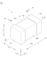
- FIG. 1 is an external perspective view of a multilayer ceramic capacitor according to the present embodiment.
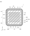
- FIG. 2 is a cross-sectional view of the multilayer ceramic capacitor shown in FIG. 1 taken along line II-II.
- 3 is a sectional view taken along line III-III of the multilayer ceramic capacitor shown in FIG. 2.
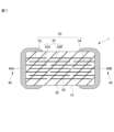
- FIG. 3 is a sectional view taken along the line IV-IV of the multilayer ceramic capacitor shown in FIG. 2.
- FIG. FIG. 3 is an enlarged view of the V section of the multilayer ceramic capacitor shown in FIG. 2, and is a schematic diagram for explaining the state of force generated on the end surface side of the multilayer ceramic capacitor.
- FIG. 2 is a schematic diagram showing an example of the configuration of a double-layered multilayer ceramic capacitor.
- FIG. 2 is a schematic diagram showing an example of the configuration of a multilayer ceramic capacitor having a triple structure.
- FIG. 2 is a schematic diagram showing an example of the configuration of a multilayer ceramic capacitor having a quadruple structure.
- FIG. 1 is an external perspective view of the multilayer ceramic capacitor 1 of this embodiment.
- Fig. 2 is a cross-sectional view taken along line II-II of the multilayer ceramic capacitor 1 in Fig. 1.
- Fig. 3 is a cross-sectional view taken along line III-III of the multilayer ceramic capacitor 1 in Fig. 2.
- Fig. 4 is a cross-sectional view taken along line IV-IV of the multilayer ceramic capacitor 1 in Fig. 2.
- the multilayer ceramic capacitor 1 includes a multilayer body 10 and an external electrode 40.
- FIGS. 1 to 4 An XYZ orthogonal coordinate system is shown in FIGS. 1 to 4.
- the length direction L of the multilayer ceramic capacitor 1 and the multilayer body 10 corresponds to the X direction.
- the width direction W of the multilayer ceramic capacitor 1 and the multilayer body 10 corresponds to the Y direction.
- the stacking direction T which is the height direction of the multilayer ceramic capacitor 1 and the multilayer body 10, corresponds to the Z direction.
- the cross section shown in FIG. 2 is also referred to as the LT cross section.
- the cross section shown in FIG. 3 is also referred to as a WT cross section.
- the cross section shown in FIG. 4 is also referred to as the LW cross section.
- the laminate 10 includes a first main surface TS1 and a second main surface TS2 that face the stacking direction T, a first side surface WS1 and a second side surface WS2 that face the width direction W that is perpendicular to the stacking direction T, and a first end surface LS1 and a second end surface LS2 that face the length direction L that is perpendicular to the stacking direction T and the width direction W.
- the laminate 10 has a substantially rectangular parallelepiped shape.
- the dimension of the laminate 10 in the length direction L is not necessarily longer than the dimension in the width direction W. It is preferable that the corners and ridges of the laminate 10 be rounded.
- a corner is a part where three sides of the laminate intersect, and a ridgeline is a part where two sides of the laminate intersect. Incidentally, unevenness or the like may be formed on a part or all of the surface constituting the laminate 10.
- the dimensions of the laminate 10 are not particularly limited, but if the dimension of the laminate 10 in the length direction L is the L dimension, it is preferable that the L dimension is 0.2 mm or more and 10 mm or less. If the dimension of the laminate 10 in the stacking direction T is the T dimension, it is preferable that the T dimension is 0.1 mm or more and 10 mm or less. If the dimension of the laminate 10 in the width direction W is the W dimension, it is preferable that the W dimension is 0.1 mm or more and 10 mm or less.
- the laminate 10 includes an inner layer part 11 and a first main surface side outer layer part 12A as a first outer layer part arranged to sandwich the inner layer part 11 in the lamination direction T. and a second main surface side outer layer portion 12B as a second outer layer portion.
- the inner layer portion 11 includes a plurality of dielectric layers 20 as a plurality of ceramic layers and a plurality of internal electrode layers 30 as a plurality of internal conductor layers. In the stacking direction T, the inner layer portion 11 includes an internal electrode layer 30 located closest to the first main surface TS1 to an internal electrode layer 30 located closest to the second main surface TS2. In the inner layer portion 11, a plurality of internal electrode layers 30 are arranged facing each other with the dielectric layer 20 interposed therebetween.
- the inner layer portion 11 is a portion that generates capacitance and essentially functions as a capacitor.
- the plurality of dielectric layers 20 are made of dielectric material.
- the dielectric material may be, for example, a dielectric ceramic containing components such as BaTiO 3 , CaTiO 3 , SrTiO 3 or CaZrO 3 . Further, the dielectric material may be one in which subcomponents such as Mn compounds, Fe compounds, Cr compounds, Co compounds, and Ni compounds are added to these main components.
- the thickness of the dielectric layer 20 is preferably 0.5 ⁇ m or more and 15 ⁇ m or less.
- the number of dielectric layers 20 to be stacked is preferably 10 or more and 700 or less.
- the number of dielectric layers 20 is the total number of the dielectric layers in the inner layer portion 11 and the dielectric layers in the first main surface side outer layer portion 12A and the second main surface side outer layer portion 12B.
- the plurality of internal electrode layers 30 have first internal electrode layers 31 as a plurality of first internal conductor layers and second internal electrode layers 32 as a plurality of second internal conductor layers.
- the plurality of first internal electrode layers 31 are arranged on the plurality of dielectric layers 20.
- the plurality of second internal electrode layers 32 are arranged on the plurality of dielectric layers 20.
- the plurality of first internal electrode layers 31 and the plurality of second internal electrode layers 32 are alternately arranged in the stacking direction T of the stacked body 10 with the dielectric layers 20 interposed therebetween.
- the first internal electrode layer 31 and the second internal electrode layer 32 are arranged with the dielectric layer 20 sandwiched therebetween.
- the first internal electrode layer 31 includes a first opposing portion 31A that faces the second internal electrode layer 32, and a first drawn-out portion 31B that is drawn out from the first opposing portion 31A to the first end surface LS1. have.
- the first drawer portion 31B is exposed at the first end surface LS1.
- the second internal electrode layer 32 includes a second opposing portion 32A that faces the first internal electrode layer 31, and a second drawn-out portion 32B that is drawn out from the second opposing portion 32A to the second end surface LS2. have.
- the second drawer portion 32B is exposed at the second end surface LS2.
- a capacitance is formed by the first opposing portion 31A and the second opposing portion 32A facing each other with the dielectric layer 20 in between, and the characteristics of a capacitor are exhibited.
- the shapes of the first opposing portion 31A and the second opposing portion 32A are not particularly limited, but are preferably rectangular. However, the rectangular corner portions may be rounded, or the rectangular corner portions may be formed obliquely.
- the shapes of the first drawer part 31B and the second drawer part 32B are not particularly limited, but are preferably rectangular. However, the rectangular corner portions may be rounded, or the rectangular corner portions may be formed obliquely.
- the dimension in the width direction W of the first facing portion 31A and the dimension in the width direction W of the first drawer portion 31B may be formed to be the same dimension, or one of the dimensions may be formed smaller.
- the dimension in the width direction W of the second facing portion 32A and the dimension in the width direction W of the second drawer portion 32B may be the same, or one of the dimensions may be formed narrower. .
- the first internal electrode layer 31 and the second internal electrode layer 32 are made of an appropriate conductive material, such as a metal such as Ni, Cu, Ag, Pd, or Au, or an alloy containing at least one of these metals. be done. When using an alloy, the first internal electrode layer 31 and the second internal electrode layer 32 may be made of, for example, an Ag--Pd alloy.
- each of the first internal electrode layer 31 and the second internal electrode layer 32 is preferably about 0.2 ⁇ m or more and 2.0 ⁇ m or less, for example.
- the total number of first internal electrode layers 31 and second internal electrode layers 32 is preferably 10 or more and 700 or less.
- the first main surface side outer layer portion 12A is located on the first main surface TS1 side of the laminate 10.
- the first main surface side outer layer portion 12A is an assembly of multiple dielectric layers 20 located between the first main surface TS1 and the internal electrode layer 30 closest to the first main surface TS1.
- the dielectric layer 20 used in the first main surface side outer layer portion 12A may be the same as the dielectric layer 20 used in the internal layer portion 11, or may be a dielectric layer made of a different material.
- the second main surface side outer layer portion 12B is located on the second main surface TS2 side of the laminate 10.
- the second main surface side outer layer portion 12B is an aggregate of a plurality of dielectric layers 20 located between the second main surface TS2 and the internal electrode layer 30 closest to the second main surface TS2.
- the dielectric layer 20 used in the second main surface side outer layer portion 12B may be the same as the dielectric layer 20 used in the inner layer portion 11, or may be a dielectric layer made of a different material. Also good.
- the laminate 10 has a counter electrode portion 11E.
- the opposing electrode portion 11E is a portion where the first opposing portion 31A of the first internal electrode layer 31 and the second opposing portion 32A of the second internal electrode layer 32 face each other.
- the counter electrode section 11E is configured as a part of the inner layer section 11.
- FIG. 4 shows the range in the width direction W and length direction L of the counter electrode portion 11E.
- the counter electrode portion 11E is also referred to as a capacitor effective portion.
- the laminate 10 has a side surface side outer layer portion.
- the side surface side outer layer portion includes a first side surface side outer layer portion WG1 and a second side surface side outer layer portion WG2.
- the first side surface side outer layer portion WG1 is a portion including the dielectric layer 20 located between the counter electrode portion 11E and the first side surface WS1.
- the second side surface side outer layer portion WG2 is a portion including the dielectric layer 20 located between the counter electrode portion 11E and the second side surface WS2.
- 3 and 4 show the range in the width direction W of the first side-side outer layer portion WG1 and the second side-side outer layer portion WG2.
- the side surface side outer layer portion is also referred to as a W gap or a side gap.
- the laminate 10 has an outer layer portion on the end surface side.
- the end surface side outer layer portion includes a first end surface side outer layer portion LG1 and a second end surface side outer layer portion LG2.
- the first end surface side outer layer portion LG1 is a portion including the dielectric layer 20 located between the counter electrode portion 11E and the first end surface LS1.
- the second end surface side outer layer portion LG2 is a portion including the dielectric layer 20 located between the counter electrode portion 11E and the second end surface LS2.
- 2 and 4 show the range in the length direction L of the first end surface side outer layer portion LG1 and the second end surface side outer layer portion LG2.
- the end surface side outer layer portion is also referred to as an L gap or an end gap.
- the external electrode 40 includes a first external electrode 40A arranged on the first end surface LS1 side and a second external electrode 40B arranged on the second end surface LS2 side.
- the first external electrode 40A is arranged on the first end surface LS1.
- the first external electrode 40A is connected to the first internal electrode layer 31.
- the first external electrode 40A is also arranged on a part of the first main surface TS1 and a part of the second main surface TS2, as well as a part of the first side surface WS1 and a part of the second side surface WS2. You can leave it there.
- the first external electrode 40A extends from above the first end surface LS1 to a part of the first main surface TS1 and a part of the second main surface TS2, and a part of the first side surface WS1 and It is formed to extend to a part of the second side surface WS2.
- the second external electrode 40B is disposed on the second end face LS2.
- the second external electrode 40B is connected to the second internal electrode layer 32.
- the second external electrode 40B may also be disposed on a portion of the first main surface TS1 and a portion of the second main surface TS2, as well as a portion of the first side surface WS1 and a portion of the second side surface WS2.
- the second external electrode 40B is formed extending from the second end face LS2 to a portion of the first main surface TS1 and a portion of the second main surface TS2, as well as a portion of the first side surface WS1 and a portion of the second side surface WS2.
- the first opposing portion 31A of the first internal electrode layer 31 and the second opposing portion 32A of the second internal electrode layer 32 are opposed to each other with the dielectric layer 20 in between. This creates a capacitance. Therefore, capacitor characteristics are developed between the first external electrode 40A to which the first internal electrode layer 31 is connected and the second external electrode 40B to which the second internal electrode layer 32 is connected.
- the first external electrode 40A includes a first base electrode layer 50A containing a metal component, a first conductive resin layer 60A disposed on the first base electrode layer 50A, and a first conductive resin layer. and a first plating layer 70A disposed on the plating layer 60A.
- the first plating layer 70A has a first Ni plating layer 71A as a lower plating layer and a first Sn plating layer 72A as an upper plating layer.
- the second external electrode 40B includes a second base electrode layer 50B containing a metal component, a second conductive resin layer 60B disposed on the second base electrode layer 50B, and a second conductive resin layer. and a second plating layer 70B disposed on the second plating layer 60B.
- the second plating layer 70B has a second Ni plating layer 71B as a lower plating layer and a second Sn plating layer 72B as an upper plating layer.
- the first Ni plating layer 71A includes a first end-side Ni plating layer 71A1 and a first side-side Ni plating layer 71A2, as shown in FIGS. 2 and 4.
- the first end of the first Ni plating layer 71A refers to a portion of the first Ni plating layer 71A that is closer to the second end surface LS2 than the first conductive resin layer 60A in the length direction L. .
- the second Ni plating layer 71B has a second end surface side Ni plating layer 71B1 and a second side surface side Ni plating layer 71B2 as shown in Figures 2 and 4.
- the second end of the second Ni plating layer 71B refers to the portion of the second Ni plating layer 71B that is closer to the first end surface LS1 side than the second conductive resin layer 60B in the length direction L.
- the basic configuration of each layer constituting the first external electrode 40A and the second external electrode 40B is the same. Further, the first external electrode 40A and the second external electrode 40B are generally symmetrical with respect to the LW cross section at the center in the length direction L of the multilayer ceramic capacitor 1. Therefore, unless it is necessary to specifically explain the first external electrode 40A and the second external electrode 40B, the first external electrode 40A and the second external electrode 40B are collectively referred to as the external electrode 40. There are cases. In addition, if it is not necessary to specifically explain the first base electrode layer 50A and the second base electrode layer 50B, the first base electrode layer 50A and the second base electrode layer 50B are collectively referred to as the base electrode layer 50A and the second base electrode layer 50B.
- the first conductive resin layer 60A and the second conductive resin layer 60B may be collectively referred to as the conductive resin layer 60.
- the first plating layer 70A and the second plating layer 70B are collectively referred to as the plating layer 70. There are cases.
- the first Ni plating layer 71A and the second Ni plating layer 71B are collectively referred to as Ni plating layer 71A and second Ni plating layer 71B. It may be called a plating layer 71.
- the first Sn plating layer 72A and the second Sn plating layer 72B are collectively referred to as Sn plating layer 72A and second Sn plating layer 72B. It may be called a plating layer 72.
- the first end-face side Ni plating layer 71A1 and the second end-face side Ni plating layer 71B1 may be collectively referred to as the end surface side Ni plating layer 711. If it is not necessary to specifically distinguish and explain the first side Ni plating layer 71A2 and the second side Ni plating layer 71B2, the first side Ni plating layer 71A2 and the second side Ni plating layer 71B2 may be collectively referred to as the side Ni plating layer 712. Further, if there is no need to specifically distinguish between the first end surface LS1 and the second end surface LS2, the first end surface LS1 and the second end surface LS2 may be collectively referred to as the end surface LS.
- the base electrode layer 50 has a first base electrode layer 50A and a second base electrode layer 50B.
- the first base electrode layer 50A is arranged on the first end surface LS1.
- the first base electrode layer 50A is connected to the first internal electrode layer 31. Further, the first base electrode layer 50A is also applied to a part of the first main surface TS1, a part of the second main surface TS2, a part of the first side surface WS1, and a part of the second side surface WS2. may be placed.
- the first base electrode layer 50A extends from above the first end surface LS1 to a part of the first main surface TS1, a part of the second main surface TS2, and a part of the first side surface WS1. and a part of the second side surface WS2.
- the second base electrode layer 50B is arranged on the second end surface LS2.
- the second base electrode layer 50B is connected to the second internal electrode layer 32. Further, the second base electrode layer 50B is also applied to a part of the first main surface TS1, a part of the second main surface TS2, a part of the first side surface WS1, and a part of the second side surface WS2. may be placed.
- the second base electrode layer 50B extends from above the second end surface LS2 to a part of the first main surface TS1, a part of the second main surface TS2, and a part of the first side surface WS1. and a part of the second side surface WS2.
- the first base electrode layer 50A and the second base electrode layer 50B of this embodiment are baked layers.
- the baking layer contains a metal component and either a glass component or a ceramic component, or both.
- the metal component includes, for example, at least one selected from Cu, Ni, Ag, Pd, Ag-Pd alloy, Au, and the like.
- the glass component includes, for example, at least one selected from B, Si, Ba, Mg, Al, Li, and the like. When a glass component is present, it can assist in sintering the metal component in the underlying electrode layer and promote sintering.
- the same type of ceramic material as the dielectric layer 20 may be used, or a different type of ceramic material may be used.
- the ceramic component includes, for example, at least one selected from BaTiO 3 , CaTiO 3 , (Ba,Ca)TiO 3 , SrTiO 3 , CaZrO 3 , and the like.
- the baked layer is, for example, a layered product coated with a conductive paste containing glass and metal and baked.
- the baked layer may be obtained by simultaneously firing a multilayer chip having internal electrodes and a dielectric layer and a conductive paste applied to the multilayer chip, or by baking a multilayer chip having internal electrodes and a dielectric layer to obtain a multilayer body.
- the laminate may then be coated with a conductive paste and baked. Note that when firing the multilayer chip having internal electrodes and dielectric layers and the conductive paste applied to the multilayer chip at the same time, the baked layer is formed by baking a ceramic material added instead of a glass component. It is preferable. In this case, it is particularly preferable to use the same type of ceramic material as the dielectric layer 20 as the added ceramic material.
- the baking layer may have multiple layers.
- the thickness in the length direction of the first base electrode layer 50A located on the first end surface LS1 is, for example, about 2 ⁇ m or more and 220 ⁇ m or less at the center of the first base electrode layer 50A in the stacking direction T and the width direction W. It is preferable that
- the thickness in the length direction of the second base electrode layer 50B located on the second end surface LS2 is, for example, about 2 ⁇ m or more and 220 ⁇ m or less at the center of the second base electrode layer 50B in the stacking direction T and the width direction W. It is preferable that
- the first base electrode layer 50A When the first base electrode layer 50A is also provided on a part of at least one of the first main surface TS1 or the second main surface TS2, the first base electrode layer 50A provided on this part
- the thickness in the stacking direction is preferably, for example, approximately 4 ⁇ m or more and 40 ⁇ m or less at the central portion in the length direction L and width direction W of the first base electrode layer 50A provided in this portion.
- the width of the first base electrode layer 50A provided on this part is preferably, for example, about 4 ⁇ m or more and 40 ⁇ m or less in the central portion of the first base electrode layer 50A provided in this portion in the length direction L and the stacking direction T.
- the second base electrode layer 50B When the second base electrode layer 50B is also provided on a part of at least one of the first main surface TS1 or the second main surface TS2, the second base electrode layer 50B provided on this part
- the thickness in the stacking direction is preferably, for example, approximately 4 ⁇ m or more and 40 ⁇ m or less at the central portion in the length direction L and width direction W of the second base electrode layer 50B provided in this portion.
- the width of the second base electrode layer 50B provided on this part is preferably, for example, approximately 4 ⁇ m or more and 40 ⁇ m or less at the central portion in the length direction L and the stacking direction T of the second base electrode layer 50B provided in this portion.
- the external electrode 40 has a conductive resin layer 60 containing a resin component and a metal component disposed on the base electrode layer 50.
- the conductive resin layer 60 includes a first conductive resin layer 60A and a second conductive resin layer 60B.
- the first conductive resin layer 60A is arranged to cover the first base electrode layer 50A. Further, it is preferable that the end portion of the first conductive resin layer 60A is in contact with the laminate 10. The end portion of the first conductive resin layer 60A refers to a portion of the first conductive resin layer 60A that is closer to the second end surface LS2 than the first base electrode layer 50A in the length direction L.
- the second conductive resin layer 60B is arranged to cover the second base electrode layer 50B. Further, it is preferable that the end portion of the second conductive resin layer 60B is in contact with the laminate 10. The end portion of the second conductive resin layer 60B refers to a portion of the second conductive resin layer 60B that is closer to the first end surface LS1 than the second base electrode layer 50B in the length direction L.
- the thickness in the length direction of the first conductive resin layer 60A located on the first end surface LS1 side is, for example, 10 ⁇ m or more at the center of the first conductive resin layer 60A in the stacking direction T and the width direction W.
- the thickness is preferably about 200 ⁇ m or less.
- the thickness in the length direction of the second conductive resin layer 60B located on the second end surface LS2 side is, for example, 10 ⁇ m or more at the center of the second conductive resin layer 60B in the lamination direction T and width direction W.
- the thickness is preferably about 200 ⁇ m or less.
- the first conductive resin layer 60A When the first conductive resin layer 60A is also provided on a part of the first main surface TS1 side and a part of the second main surface TS2 side, the first conductive resin layer provided in this part
- the thickness of the first conductive resin layer 60A in the stacking direction T is preferably, for example, about 10 ⁇ m or more and 200 ⁇ m or less at the center in the length direction L and width direction W of the first conductive resin layer 60A provided in this portion.
- the first conductive resin layer 60A When the first conductive resin layer 60A is also provided on a part of the first side surface WS1 side and a part of the second side surface WS2 side, the first conductive resin layer 60A provided on this part is
- the thickness in the width direction W is preferably, for example, about 10 ⁇ m or more and 200 ⁇ m or less at the central portion in the length direction L and lamination direction T of the first conductive resin layer 60A provided in this portion.
- the second conductive resin layer 60B When the second conductive resin layer 60B is also provided on a part of the first main surface TS1 side and a part of the second main surface TS2 side, the second conductive resin layer provided in this part
- the thickness of the second conductive resin layer 60B in the stacking direction T is preferably, for example, about 10 ⁇ m or more and 200 ⁇ m or less at the center in the length direction L and width direction W of the second conductive resin layer 60B provided in this portion.
- the thickness in the width direction W of the second conductive resin layer 60B provided on this portion is preferably, for example, about 10 ⁇ m or more and 200 ⁇ m or less at the center in the length direction L and stacking direction T of the second conductive resin layer 60B provided on this portion.
- the conductive resin layer 60 is disposed on the base electrode layer 50.
- a plating layer 70 is disposed so as to cover the conductive resin layer 60.
- the plating layer 70 has a Ni plating layer 71 and a Sn plating layer 72.
- the conductive resin layer 60 has a resin part and a conductive filler dispersed within the resin part.
- the resin portion of the conductive resin layer 60 may contain at least one selected from various known thermosetting resins such as epoxy resin, phenoxy resin, phenol resin, urethane resin, silicone resin, and polyimide resin. good. Among them, epoxy resin is one of the most suitable resins because of its excellent heat resistance, moisture resistance, adhesiveness, and the like. Moreover, it is preferable that the resin part of the conductive resin layer 60 contains a hardening agent together with a thermosetting resin. When an epoxy resin is used as the base resin, the curing agent for the epoxy resin may be various known compounds such as phenol, amine, acid anhydride, imidazole, active ester, and amide-imide.
- the conductive resin layer 60 contains such a resin portion, it is more flexible than, for example, the base electrode layer 50, which is made of a plating film or a fired product of metal components and glass components. Therefore, even if the multilayer ceramic capacitor 1 is subjected to a physical impact or an impact due to a thermal cycle, the conductive resin layer 60 functions as a buffer layer. Therefore, the conductive resin layer 60 suppresses the occurrence of cracks in the multilayer ceramic capacitor 1.
- the conductive filler exists in a substantially uniformly distributed manner within the resin part.
- the conductive filler is mainly responsible for the conductivity of the conductive resin layer 60. Specifically, when the plurality of conductive fillers come into contact with each other, a current-carrying path is formed inside the conductive resin layer 60, and conduction occurs between the base electrode layer 50 and the plating layer 70.
- the metal constituting the conductive filler may be Ag alone, an alloy containing Ag, or a metal powder whose surface is coated with Ag.
- Ag has the lowest specific resistance among metals, so it is suitable as an electrode material. Furthermore, since Ag is a noble metal, it is difficult to oxidize and has high weather resistance. Therefore, Ag metal powder is suitable as a conductive filler. Further, when using a metal powder whose surface is coated with Ag, it is preferable to use Cu, Ni, Sn, Bi, or an alloy powder containing them as the metal powder.
- the conductive filler may be Cu or Ni that has been subjected to an anti-oxidation treatment.
- the conductive filler may also be a metal powder whose surface is coated with Sn, Ni, or Cu.
- the metal powder is Ag, Cu, Ni, Sn, Bi, or an alloy powder of these.
- the shape of the conductive filler is not particularly limited.
- the conductive filler may be spherical or flat, but it is preferable to use a mixture of spherical metal powder and flat metal powder.
- the average particle diameter of the conductive filler may be, for example, 0.3 ⁇ m or more and 10 ⁇ m or less.
- the average particle diameter of the conductive filler contained in the conductive resin layer 60 is calculated by using a laser diffraction particle size measurement method based on ISO 13320, regardless of the shape of the conductive filler.
- the plating layer 70 has a first plating layer 70A and a second plating layer 70B.
- the first plating layer 70A is arranged to cover the first conductive resin layer 60A.
- the first plating layer 70A covers a portion of the first main surface TS1, a portion of the second main surface TS2, and a portion of the first side surface WS1 from above the first end surface LS1. and is arranged so as to extend to a part of the second side surface WS2. More specifically, in the first plating layer 70A, the above-mentioned first end-side Ni plating layer 71A1 is disposed on the first end surface LS1, and the above-mentioned first side-side Ni plating layer 71A2 is disposed on the first end surface LS1.
- the second plating layer 70B is arranged to cover the second conductive resin layer 60B.
- the second plating layer 70B covers a portion of the first main surface TS1, a portion of the second main surface TS2, and a portion of the first side surface WS1 from above the first end surface LS1. and is arranged so as to extend to a part of the second side surface WS2. More specifically, in the second plating layer 70B, the second end surface side Ni plating layer 71B1 described above is disposed on the second end surface LS2, and the second side surface side Ni plating layer 71B2 described above is disposed on the second end surface LS2.
- the plating layer 70 preferably has a two-layer structure of a Ni plating layer 71 and a Sn plating layer 72. It is preferable that a first Sn plating layer 72A is disposed on the first Ni plating layer 71A, and a second Sn plating layer 72B is disposed on the second Ni plating layer 71B. It is preferable.
- the Ni plating layer 71 prevents the base electrode layer 50 and the conductive resin layer 60 from being eroded by solder when the multilayer ceramic capacitor 1 is mounted.
- the Sn plating layer 72 improves solder wettability when mounting the multilayer ceramic capacitor 1. This facilitates mounting of the multilayer ceramic capacitor 1.
- each of the first Ni plating layer 71A and the first Sn plating layer 72A is preferably 1 ⁇ m or more and 15 ⁇ m or less.
- each of the second Ni plating layer 71B and the second Sn plating layer 72B is preferably 1 ⁇ m or more and 15 ⁇ m or less.
- FIG. 5 is an enlarged view of the V section of the multilayer ceramic capacitor 1 shown in FIG. 2, and is a schematic diagram for explaining the state of force generated on the end surface LS side of the multilayer ceramic capacitor 1.
- the conductive resin layer 60 is arranged on the base electrode layer 50.
- a plating layer 70 which will be described later, is arranged to cover the conductive resin layer 60.
- the plating layer 70 has a Ni plating layer 71 and a Sn plating layer 72.
- the Ni plating layer 71 includes an end side Ni plating layer 711 and a side surface side Ni plating layer 712.
- the Ni plating layer 71 is formed so that tensile stress is uniformly generated as a whole in a direction intersecting the thickness direction of the plating layer 70. In other words, tensile stress remains inside the Ni plating layer 71 as internal stress. Tensile stress is generated in the end face side Ni plating layer 711 in a direction intersecting the thickness direction of the plating layer 70, and the end face side Ni plating layer 711 tends to shrink in the direction intersecting the thickness direction of the plating layer 70. As shown in FIG. 5, the side surface side Ni plating layers 712 formed on both ends with the end surface side Ni plating layer 711 in between are each pulled toward the center of the end surface side Ni plating layer 711.
- the side surface side Ni plating layers 712 formed on both sides of the end surface side Ni plating layer 711 are each subjected to a force in the direction of pressing the conductive resin layer 60 against the base electrode layer 50 .
- the conductivity of the conductive resin layer 60 is improved, and the ESR (Equivalent Series Resistance) is reduced.
- the side Ni plating layer 712 tends to shrink in the direction intersecting the thickness direction of the plating layer 70 due to the generation of tensile stress in the direction intersecting the thickness direction of the plating layer 70 . Therefore, the side surface side Ni plating layer 712 is tightened to the conductive resin layer 60 in the circumferential direction of the side surface side Ni plating layer 712, and the end surface side Ni plating layer 711 is pulled in the length direction L. Layer 60 is pressed against base electrode layer 50. This improves the conductivity of the conductive resin layer 60 and has the effect of reducing ESR.
- the tensile stress is 50 MPa or more. Thereby, the ESR reduction effect can be further enhanced.
- the stress of the Ni plating layer 71 becomes greater than 206 MPa, it becomes difficult to manufacture the multilayer ceramic capacitor 1, so the tensile stress is preferably 206 MPa or less. Thereby, the multilayer ceramic capacitor 1 can be easily manufactured while further enhancing the ESR reduction effect.
- the dimension in the length direction of the multilayer ceramic capacitor 1 including the laminate 10 and the external electrode 40 is the L dimension
- the L dimension is preferably 0.2 mm or more and 10 mm or less.
- the T dimension is preferably 0.1 mm or more and 10 mm or less.
- the W dimension is preferably 0.1 mm or more and 10 mm or less.
- a dielectric sheet for the dielectric layer 20 and a conductive paste for the internal electrode layer 30 are prepared.
- the conductive paste for the dielectric sheet and internal electrodes contains a binder and a solvent.
- the binder and solvent may be known ones.
- a conductive paste for the internal electrode layer 30 is printed in a predetermined pattern on the dielectric sheet by, for example, screen printing or gravure printing. As a result, a dielectric sheet on which the pattern of the first internal electrode layer 31 is formed and a dielectric sheet on which the pattern of the second internal electrode layer 32 is formed are prepared.
- a portion that will become the first main surface side outer layer portion 12A on the first main surface TS1 side is formed.
- a dielectric sheet with a pattern of the first internal electrode layer 31 printed thereon and a dielectric sheet with a pattern of the second internal electrode layer 32 printed thereon are sequentially laminated to form the inner layer section 11. parts are formed.
- a second main surface side outer layer portion 12B on the second main surface TS2 side is formed. A part is formed. In this way, a laminated sheet is produced.
- a laminated block is produced by pressing the laminated sheet in the lamination direction by means such as a hydrostatic press.
- laminated chips are cut out.
- the corners and ridges of the laminated chip may be rounded by barrel polishing or the like.
- the stacked body 10 is produced by firing the stacked chips.
- the firing temperature depends on the materials of the dielectric layer 20 and the internal electrode layer 30, it is preferably 900° C. or more and 1400° C. or less.
- a conductive paste that will become the base electrode layer 50 is applied to both end surfaces of the laminate 10.
- the base electrode layer 50 is a baked layer.
- a conductive paste containing a glass component and a metal is applied to the laminate 10 by a method such as dipping.
- a baking process is then performed to form the base electrode layer 50.
- the temperature of the baking process at this time is preferably 700°C or higher and 950°C or lower.
- a conductive resin layer 60 is formed. Note that the conductive resin layer 60 may be formed on the surface of the base electrode layer 50 or directly on the laminate 10. In this embodiment, the conductive resin layer 60 is formed on the surface of the base electrode layer 50.
- a conductive resin paste is prepared in which a conductive filler is dispersed in a thermosetting resin as a base resin that will become the resin part.
- This conductive resin paste is produced by stirring and mixing a thermosetting resin and a conductive filler. Therefore, the conductive filler exists in the conductive resin paste in a uniformly distributed manner.
- the thermosetting resin is, for example, an epoxy resin.
- the conductive filler is, for example, Ag metal powder.
- a conductive resin paste is applied onto the base electrode layer 50 using a dipping method, and heat treatment is performed at a temperature of 200° C. or higher and 550° C. or lower. As a result, the resin portion is thermally cured, and the conductive resin layer 60 is formed.
- the atmosphere during the heat treatment at this time is preferably a N 2 atmosphere. Further, in order to prevent resin scattering and oxidation of various metal components, the oxygen concentration is preferably suppressed to 100 ppm or less.
- a plating layer 70 is formed on the surface of the conductive resin layer 60.
- a Ni plating layer 71 and a Sn plating layer 72 are formed on the conductive resin layer 60.
- Ni plating layer 71 and Sn plating layer 72 are sequentially formed using an electric field plating method.
- the plating method it is preferable to use barrel plating, for example.
- the stress generated throughout the first Ni plating layer 71A and the second Ni plating layer 71B of the present invention can be controlled by the following method.
- the stress generated in plating varies depending on the current density applied during film formation.
- the current density applied to the multilayer ceramic capacitor 1 is random.
- the average current density applied to each tip until it reaches a thickness of It is the same on both sides of the tip of the Ni plating layer. Therefore, the same stress is applied to all surfaces of the Ni plating layer 70 on the first main surface TS1, the second main surface TS2, the first side surface WS1, and the second side surface WS2.
- the first Ni layer 71A and the second Ni plating layer 71B can be formed by using a plating bath using a plating solution prepared by adjusting the amounts of Ni sulfate and Ni sulfamate, for example. By adjusting the ratio of Ni sulfate and Ni sulfamate in the plating solution, the value of residual stress inside the Ni plating layer 71 to be formed can be adjusted.
- a Sn plating layer 72 is further formed on the Ni plating layer 71, a first Sn plating layer 72A is on the first Ni plating layer 71A, and a second Sn plating layer 72A is on the second Ni plating layer 71B.
- a Sn plating layer 72B was formed.
- an electrolytic plating method is used.
- barrel plating is preferably used. Thereby, when mounting the multilayer ceramic capacitor 1, the wettability of the solder used for mounting can be improved, and the mounting can be easily performed.
- the multilayer ceramic capacitor 1 is manufactured by the above manufacturing method.
- the multilayer ceramic capacitor 1 of this embodiment provides the following advantages:
- ceramic electronic components such as multilayer ceramic capacitors have come to be used in harsher environments than before.
- electronic components used in mobile devices such as mobile phones and portable music players are required to withstand impact when dropped.
- ECUs Electronic Control Units
- thermal cycles it is necessary to prevent cracks from occurring in the electronic component even when subjected to bending stress generated by thermal expansion and contraction of the mounting board due to thermal cycles.
- thermosetting conductive resin paste for the external electrodes of ceramic electronic components as a measure to prevent cracks from forming in the ceramic electronic component body even in harsh environments.
- an epoxy thermosetting resin layer is formed between a conventional electrode layer and a Ni plating layer.
- the epoxy thermosetting resin layer prevents cracks from forming in the ceramic electronic component body.
- the Ni plating layer presses the conductive resin layer against the base electrode layer side, compressing the conductive resin layer, and reducing the conductivity in the conductive resin layer.
- the amount of contact between the fillers increases, and the conductivity of the conductive resin layer can be improved. Therefore, a multilayer ceramic electronic component with reduced ESR and improved initial characteristics can be provided.
- the multilayer ceramic capacitor 1 (multilayer ceramic electronic component 1) according to the present embodiment includes a plurality of stacked dielectric layers 20 (ceramic layers 20), and has a first main surface TS1 facing the stacking direction T. and a second main surface TS2, a first side surface WS1 and a second side surface WS2 facing in the width direction W perpendicular to the stacking direction T, and a second side surface WS2 facing in the length direction L perpendicular to the stacking direction T and width direction W.
- a stacked body 10 having a first end surface LS1 and a second end surface LS2, and a first internal electrode layer 31 (first an internal conductor layer 31), a second internal electrode layer 32 (second internal conductor layer 32) disposed on the plurality of dielectric layers 20 and exposed to the second end surface LS2, and a first end surface LS1.
- the first external electrode 40A does not contain a metal component.
- the second external electrode 40B includes a second base electrode layer 50B containing a metal component and a first Ni plating layer 71A disposed on the second base electrode layer 50B. It has a second conductive resin layer 60B containing a thermosetting resin and a metal component, and a second Ni plating layer 71B disposed on the second conductive resin layer 60B, and has a first Ni plating layer. Tensile stress remains as internal stress inside the layer 71A, and tensile stress remains as internal stress inside the second Ni plating layer 71B.
- the tensile stress generated in the first Ni plating layer 71A and the second Ni plating layer 71B is 50 MPa or more.
- the multilayer ceramic capacitor 1 of this embodiment includes a first Sn plating layer 72A disposed on the first Ni plating layer 71A and a second Sn plating layer disposed on the second Ni plating layer 71B. It has a plating layer 72B.
- the first base electrode layer 50A includes a glass component or a ceramic component
- the second base electrode layer 50B includes a glass component or a ceramic component.
- multilayer ceramic capacitors having the structures shown in FIGS. 1 to 4 were manufactured as samples of Examples and Comparative Examples.
- samples were prepared by controlling the stress of the Ni plating layer using the method described in the manufacturing method above to achieve the stress shown in Table 1, and 22 samples were prepared for each stress condition. was created.
- the specifications of the multilayer ceramic capacitor are as follows.
- Thickness 15 ⁇ m Thickness of the base electrode layer at the center in the length direction of the base electrode layer located on the first main surface, the second main surface, the first side surface, and the second side surface: 4 ⁇ m
- Conductive resin layer Conductive resin layer portion Conductive filler: Ag Resin: Epoxy thermosetting temperature: 200°C Thickness at the center in the height direction of the first conductive resin layer portion located on the first end face and the second end face: 20 ⁇ m Thickness of the base electrode layer at the center in the length direction of the base electrode layer located on the first main surface, the second main surface, the first side surface, and the second side surface: 20 ⁇ m
- the multilayer ceramic capacitor 1 was immersed in the liquid for 5 minutes using a metal stripping agent (Melstrip (registered trademark) HN980M manufactured by Meltex Co., Ltd.), and then washed with water to peel off the Sn plating layer.
- a metal stripping agent Melstrip (registered trademark) HN980M manufactured by Meltex Co., Ltd.
- HN980M manufactured by Meltex Co., Ltd.
- the second Measurements were made using X-ray diffraction ( ⁇ -XRD (X-ray Diffraction)) at approximately the center of each surface of the Ni plating layer located on side surface WS2 in a range of ⁇ 100 ⁇ m.
- the stress in the Ni plating layer on the first main surface TS1 is the stress in the length direction L of each of the first Ni plating layer 71A and the second Ni plating layer 71B on the first main surface TS1.
- the measurement was performed targeting the center and the center position in the width direction W.
- the stress in the Ni plating layer on the second main surface TS2 is at the center and the width in the length direction L of each of the first Ni plating layer 71A and the second Ni plating layer 71B on the second main surface TS2. Measurements were made targeting the center position in direction W.
- the stress in the Ni plating layer on the first side surface WS1 is at the center of the length direction L of each of the first Ni plating layer 71A and the second Ni plating layer 71B on the first side surface WS1 and in the stacking direction T. Measurements were made targeting the center position.
- the stress in the Ni plating layer on the second side surface WS2 is applied to the center of the length direction L of each of the first Ni plating layer 71A and the second Ni plating layer 71B on the second side surface WS2 and the stacking direction T. Measurements were made targeting the center position. The two produced samples were measured, and the average value of the measured values at the eight locations was taken as the measured value of stress.
- the effects of the present invention could be made more remarkable, and a multilayer ceramic capacitor with improved initial characteristics could be provided.
- the configuration of the multilayer ceramic capacitor 1 is not limited to the configurations shown in FIGS. 1 to 4.
- the multilayer ceramic capacitor 1 may be a multilayer ceramic capacitor having a double structure, a triple structure, or a quadruple structure, as shown in FIGS. 6, 7, and 8.
- the multilayer ceramic capacitor 1 shown in FIG. 6 is a double-layered multilayer ceramic capacitor 1, and includes a first end surface as an internal electrode layer 30 in addition to a first internal electrode layer 33 and a second internal electrode layer 34. A floating internal electrode layer 35 that is not drawn out to either LS1 or second end surface LS2 is provided.
- the multilayer ceramic capacitor 1 shown in FIG. 7 is a triple-structured multilayer ceramic capacitor 1 including a first floating internal electrode layer 35A and a second floating internal electrode layer 35B as the floating internal electrode layers 35.
- the multilayer ceramic capacitor 1 shown in FIG. 8 has a quadruple structure including a first floating internal electrode layer 35A, a second floating internal electrode layer 35B, and a third floating internal electrode layer 35C as the floating internal electrode layers 35.
- the multilayer ceramic capacitor 1 has a structure in which the opposing electrode portion is divided into a plurality of parts. As a result, a plurality of capacitor components are formed between the opposing internal electrode layers 30, and these capacitor components are connected in series. Therefore, the voltage applied to each capacitor component is reduced, and the multilayer ceramic capacitor 1 can have a high withstand voltage.
- the multilayer ceramic capacitor 1 of this embodiment may have a multi-connection structure of four or more units.
- the multilayer ceramic capacitor 1 may be of a two-terminal type with two external electrodes, or may be of a multi-terminal type with a large number of external electrodes.
- a multilayer ceramic capacitor in which the dielectric layer 20 made of dielectric ceramic is used as a ceramic layer is exemplified as a multilayer ceramic electronic component.
- the multilayer ceramic electronic component of the present disclosure is not limited thereto.
- the ceramic electronic components of the present disclosure can be applied to various laminated ceramic electronic components such as piezoelectric components using piezoelectric ceramics as ceramic layers, thermistors using semiconductor ceramics as ceramic layers, and inductors using magnetic ceramics as ceramic layers. It can also be applied to parts.
- Piezoelectric ceramics include PZT (lead zirconate titanate) ceramics
- semiconductor ceramics include spinel ceramics
- magnetic ceramics include ferrite and other ceramics.
- the present invention is not limited to the configuration of the above-described embodiments, and can be modified and applied as appropriate without changing the gist of the present invention. Note that the present invention also includes a combination of two or more of the individual desirable configurations described in the above embodiments.
- It includes a plurality of laminated ceramic layers, and has a first main surface and a second main surface facing each other in the height direction, and a first side surface and a second side surface facing each other in the width direction perpendicular to the height direction.
- the first external electrode includes a first base electrode layer containing a metal component, a first conductive resin layer containing a thermosetting resin and a metal component disposed on the first base electrode layer, a first Ni plating layer disposed on the first conductive resin layer,
- the second external electrode includes a second base electrode layer containing a metal component, and a second conductive resin layer containing a thermosetting resin and a metal component disposed on the second base electrode layer.
- a first Sn plating layer is arranged on the first Ni plating layer, The multilayer ceramic electronic component according to ⁇ 1> or ⁇ 2>, wherein a second Sn plating layer is disposed on the second Ni plating layer.
- the first base electrode layer contains a glass component or a ceramic component, The multilayer ceramic electronic component according to any one of ⁇ 1> to ⁇ 3>, wherein the second base electrode layer contains a glass component or a ceramic component.
- Multilayer ceramic capacitor (multilayer ceramic electronic component) 10 Laminated body 20 Dielectric layer (ceramic layer) 31 First internal electrode layer (first internal conductor layer) 32 Second internal electrode layer (second internal conductor layer) 40A First external electrode 40B Second external electrode 50A First base electrode layer 50B Second base electrode layer 60A First conductive resin layer 60B Second conductive resin layer 71A First Ni plating layer 71B Second Ni plating layer T Height direction TS1 First main surface TS2 Second main surface W Width direction WS1 First side surface WS2 Second side surface L Length direction LS1 First end surface LS2 Second end surface
Landscapes
- Engineering & Computer Science (AREA)
- Power Engineering (AREA)
- Microelectronics & Electronic Packaging (AREA)
- Manufacturing & Machinery (AREA)
- Chemical & Material Sciences (AREA)
- Ceramic Engineering (AREA)
- Inorganic Chemistry (AREA)
- Mechanical Engineering (AREA)
- Organic Chemistry (AREA)
- Metallurgy (AREA)
- Materials Engineering (AREA)
- Chemical Kinetics & Catalysis (AREA)
- Physics & Mathematics (AREA)
- Dispersion Chemistry (AREA)
- Spectroscopy & Molecular Physics (AREA)
- Fixed Capacitors And Capacitor Manufacturing Machines (AREA)
- Ceramic Capacitors (AREA)
Priority Applications (5)
| Application Number | Priority Date | Filing Date | Title |
|---|---|---|---|
| KR1020257001725A KR20250023559A (ko) | 2022-09-21 | 2023-07-19 | 적층 세라믹 전자부품 |
| CN202380051811.1A CN119404267A (zh) | 2022-09-21 | 2023-07-19 | 层叠陶瓷电子部件 |
| EP23867879.1A EP4576139A1 (en) | 2022-09-21 | 2023-07-19 | Multilayer ceramic electronic component |
| JP2024548108A JPWO2024062753A1 (https=) | 2022-09-21 | 2023-07-19 | |
| US18/925,488 US20250054698A1 (en) | 2022-09-21 | 2024-10-24 | Multilayer ceramic electronic component |
Applications Claiming Priority (2)
| Application Number | Priority Date | Filing Date | Title |
|---|---|---|---|
| JP2022-150525 | 2022-09-21 | ||
| JP2022150525 | 2022-09-21 |
Related Child Applications (1)
| Application Number | Title | Priority Date | Filing Date |
|---|---|---|---|
| US18/925,488 Continuation US20250054698A1 (en) | 2022-09-21 | 2024-10-24 | Multilayer ceramic electronic component |
Publications (1)
| Publication Number | Publication Date |
|---|---|
| WO2024062753A1 true WO2024062753A1 (ja) | 2024-03-28 |
Family
ID=90454402
Family Applications (1)
| Application Number | Title | Priority Date | Filing Date |
|---|---|---|---|
| PCT/JP2023/026360 Ceased WO2024062753A1 (ja) | 2022-09-21 | 2023-07-19 | 積層セラミック電子部品 |
Country Status (6)
| Country | Link |
|---|---|
| US (1) | US20250054698A1 (https=) |
| EP (1) | EP4576139A1 (https=) |
| JP (1) | JPWO2024062753A1 (https=) |
| KR (1) | KR20250023559A (https=) |
| CN (1) | CN119404267A (https=) |
| WO (1) | WO2024062753A1 (https=) |
Citations (6)
| Publication number | Priority date | Publication date | Assignee | Title |
|---|---|---|---|---|
| JPH01162771A (ja) | 1987-12-19 | 1989-06-27 | Fujitsu Ltd | 熱処理装置 |
| JPH11162771A (ja) | 1997-11-25 | 1999-06-18 | Kyocera Corp | 積層セラミックコンデンサ |
| JP2000357627A (ja) * | 1999-06-15 | 2000-12-26 | Mitsubishi Materials Corp | チップ型電子部品 |
| JP2009267146A (ja) * | 2008-04-25 | 2009-11-12 | Murata Mfg Co Ltd | 積層セラミック電子部品 |
| JP2016009836A (ja) * | 2014-06-26 | 2016-01-18 | 株式会社村田製作所 | 積層セラミック電子部品 |
| JP2021125673A (ja) * | 2020-02-10 | 2021-08-30 | 株式会社村田製作所 | 積層セラミックコンデンサ |
-
2023
- 2023-07-19 JP JP2024548108A patent/JPWO2024062753A1/ja active Pending
- 2023-07-19 KR KR1020257001725A patent/KR20250023559A/ko active Pending
- 2023-07-19 CN CN202380051811.1A patent/CN119404267A/zh active Pending
- 2023-07-19 WO PCT/JP2023/026360 patent/WO2024062753A1/ja not_active Ceased
- 2023-07-19 EP EP23867879.1A patent/EP4576139A1/en active Pending
-
2024
- 2024-10-24 US US18/925,488 patent/US20250054698A1/en active Pending
Patent Citations (6)
| Publication number | Priority date | Publication date | Assignee | Title |
|---|---|---|---|---|
| JPH01162771A (ja) | 1987-12-19 | 1989-06-27 | Fujitsu Ltd | 熱処理装置 |
| JPH11162771A (ja) | 1997-11-25 | 1999-06-18 | Kyocera Corp | 積層セラミックコンデンサ |
| JP2000357627A (ja) * | 1999-06-15 | 2000-12-26 | Mitsubishi Materials Corp | チップ型電子部品 |
| JP2009267146A (ja) * | 2008-04-25 | 2009-11-12 | Murata Mfg Co Ltd | 積層セラミック電子部品 |
| JP2016009836A (ja) * | 2014-06-26 | 2016-01-18 | 株式会社村田製作所 | 積層セラミック電子部品 |
| JP2021125673A (ja) * | 2020-02-10 | 2021-08-30 | 株式会社村田製作所 | 積層セラミックコンデンサ |
Also Published As
| Publication number | Publication date |
|---|---|
| US20250054698A1 (en) | 2025-02-13 |
| JPWO2024062753A1 (https=) | 2024-03-28 |
| KR20250023559A (ko) | 2025-02-18 |
| EP4576139A1 (en) | 2025-06-25 |
| CN119404267A (zh) | 2025-02-07 |
Similar Documents
| Publication | Publication Date | Title |
|---|---|---|
| JP7567146B2 (ja) | 積層セラミック電子部品及びその実装基板 | |
| US11062848B2 (en) | Multilayer ceramic electronic component | |
| JP5801328B2 (ja) | 積層セラミックキャパシタ及びその製造方法 | |
| KR20150018650A (ko) | 적층 세라믹 전자 부품 및 그 실장 기판과 제조 방법 | |
| JP2022191909A (ja) | 積層セラミック電子部品 | |
| KR101719838B1 (ko) | 도전성 수지 조성물 및 이를 포함하는 적층 세라믹 전자 부품 | |
| JP2022191911A (ja) | 積層セラミック電子部品 | |
| JP2023087534A (ja) | 積層セラミックコンデンサ | |
| WO2023095620A1 (ja) | 積層セラミック電子部品 | |
| JP2026069621A (ja) | 積層セラミックコンデンサ | |
| JP2022085688A (ja) | 積層セラミック電子部品 | |
| WO2024135256A1 (ja) | 積層セラミック電子部品 | |
| WO2024062753A1 (ja) | 積層セラミック電子部品 | |
| WO2023243159A1 (ja) | 積層セラミックコンデンサ | |
| US12525403B2 (en) | Multilayer ceramic electronic component | |
| US20250279243A1 (en) | Multilayer ceramic electronic component | |
| WO2026034048A1 (ja) | 積層セラミック電子部品 | |
| WO2026069542A1 (ja) | 積層セラミック電子部品 | |
| US20250299883A1 (en) | Multilayer ceramic electronic component | |
| JP2020174073A (ja) | 積層セラミックコンデンサ | |
| KR20250144885A (ko) | 적층 세라믹 전자부품 | |
| JP2025144142A (ja) | 積層セラミック電子部品 | |
| KR20250144879A (ko) | 적층 세라믹 전자부품 | |
| JP6602925B2 (ja) | セラミック電子部品及びその製造方法 | |
| WO2026004070A1 (ja) | 積層セラミック電子部品 |
Legal Events
| Date | Code | Title | Description |
|---|---|---|---|
| 121 | Ep: the epo has been informed by wipo that ep was designated in this application |
Ref document number: 23867879 Country of ref document: EP Kind code of ref document: A1 |
|
| WWE | Wipo information: entry into national phase |
Ref document number: 2024548108 Country of ref document: JP |
|
| WWE | Wipo information: entry into national phase |
Ref document number: 202380051811.1 Country of ref document: CN |
|
| ENP | Entry into the national phase |
Ref document number: 20257001725 Country of ref document: KR Kind code of ref document: A |
|
| WWE | Wipo information: entry into national phase |
Ref document number: 1020257001725 Country of ref document: KR |
|
| WWP | Wipo information: published in national office |
Ref document number: 202380051811.1 Country of ref document: CN |
|
| WWP | Wipo information: published in national office |
Ref document number: 1020257001725 Country of ref document: KR |
|
| WWE | Wipo information: entry into national phase |
Ref document number: 202517023522 Country of ref document: IN |
|
| WWE | Wipo information: entry into national phase |
Ref document number: 2023867879 Country of ref document: EP |
|
| ENP | Entry into the national phase |
Ref document number: 2023867879 Country of ref document: EP Effective date: 20250319 |
|
| WWP | Wipo information: published in national office |
Ref document number: 202517023522 Country of ref document: IN |
|
| NENP | Non-entry into the national phase |
Ref country code: DE |
|
| WWP | Wipo information: published in national office |
Ref document number: 2023867879 Country of ref document: EP |