EP4576139A1 - Multilayer ceramic electronic component - Google Patents
Multilayer ceramic electronic component Download PDFInfo
- Publication number
- EP4576139A1 EP4576139A1 EP23867879.1A EP23867879A EP4576139A1 EP 4576139 A1 EP4576139 A1 EP 4576139A1 EP 23867879 A EP23867879 A EP 23867879A EP 4576139 A1 EP4576139 A1 EP 4576139A1
- Authority
- EP
- European Patent Office
- Prior art keywords
- layer
- electrically conductive
- plated layer
- plated
- end surface
- Prior art date
- Legal status (The legal status is an assumption and is not a legal conclusion. Google has not performed a legal analysis and makes no representation as to the accuracy of the status listed.)
- Pending
Links
Images


Classifications
-
- H—ELECTRICITY
- H01—ELECTRIC ELEMENTS
- H01G—CAPACITORS; CAPACITORS, RECTIFIERS, DETECTORS, SWITCHING DEVICES, LIGHT-SENSITIVE OR TEMPERATURE-SENSITIVE DEVICES OF THE ELECTROLYTIC TYPE
- H01G4/00—Fixed capacitors; Processes of their manufacture
- H01G4/002—Details
- H01G4/228—Terminals
- H01G4/232—Terminals electrically connecting two or more layers of a stacked or rolled capacitor
- H01G4/2325—Terminals electrically connecting two or more layers of a stacked or rolled capacitor characterised by the material of the terminals
-
- C—CHEMISTRY; METALLURGY
- C23—COATING METALLIC MATERIAL; COATING MATERIAL WITH METALLIC MATERIAL; CHEMICAL SURFACE TREATMENT; DIFFUSION TREATMENT OF METALLIC MATERIAL; COATING BY VACUUM EVAPORATION, BY SPUTTERING, BY ION IMPLANTATION OR BY CHEMICAL VAPOUR DEPOSITION, IN GENERAL; INHIBITING CORROSION OF METALLIC MATERIAL OR INCRUSTATION IN GENERAL
- C23C—COATING METALLIC MATERIAL; COATING MATERIAL WITH METALLIC MATERIAL; SURFACE TREATMENT OF METALLIC MATERIAL BY DIFFUSION INTO THE SURFACE, BY CHEMICAL CONVERSION OR SUBSTITUTION; COATING BY VACUUM EVAPORATION, BY SPUTTERING, BY ION IMPLANTATION OR BY CHEMICAL VAPOUR DEPOSITION, IN GENERAL
- C23C14/00—Coating by vacuum evaporation, by sputtering or by ion implantation of the coating forming material
- C23C14/06—Coating by vacuum evaporation, by sputtering or by ion implantation of the coating forming material characterised by the coating material
- C23C14/14—Metallic material, boron or silicon
-
- H—ELECTRICITY
- H01—ELECTRIC ELEMENTS
- H01B—CABLES; CONDUCTORS; INSULATORS; SELECTION OF MATERIALS FOR THEIR CONDUCTIVE, INSULATING OR DIELECTRIC PROPERTIES
- H01B1/00—Conductors or conductive bodies characterised by the conductive materials; Selection of materials as conductors
- H01B1/20—Conductive material dispersed in non-conductive organic material
- H01B1/22—Conductive material dispersed in non-conductive organic material the conductive material comprising metals or alloys
-
- H—ELECTRICITY
- H01—ELECTRIC ELEMENTS
- H01G—CAPACITORS; CAPACITORS, RECTIFIERS, DETECTORS, SWITCHING DEVICES, LIGHT-SENSITIVE OR TEMPERATURE-SENSITIVE DEVICES OF THE ELECTROLYTIC TYPE
- H01G4/00—Fixed capacitors; Processes of their manufacture
- H01G4/002—Details
- H01G4/018—Dielectrics
- H01G4/06—Solid dielectrics
- H01G4/08—Inorganic dielectrics
- H01G4/12—Ceramic dielectrics
- H01G4/1209—Ceramic dielectrics characterised by the ceramic dielectric material
- H01G4/1218—Ceramic dielectrics characterised by the ceramic dielectric material based on titanium oxides or titanates
- H01G4/1227—Ceramic dielectrics characterised by the ceramic dielectric material based on titanium oxides or titanates based on alkaline earth titanates
-
- H—ELECTRICITY
- H01—ELECTRIC ELEMENTS
- H01G—CAPACITORS; CAPACITORS, RECTIFIERS, DETECTORS, SWITCHING DEVICES, LIGHT-SENSITIVE OR TEMPERATURE-SENSITIVE DEVICES OF THE ELECTROLYTIC TYPE
- H01G4/00—Fixed capacitors; Processes of their manufacture
- H01G4/002—Details
- H01G4/228—Terminals
- H01G4/232—Terminals electrically connecting two or more layers of a stacked or rolled capacitor
-
- H—ELECTRICITY
- H01—ELECTRIC ELEMENTS
- H01G—CAPACITORS; CAPACITORS, RECTIFIERS, DETECTORS, SWITCHING DEVICES, LIGHT-SENSITIVE OR TEMPERATURE-SENSITIVE DEVICES OF THE ELECTROLYTIC TYPE
- H01G4/00—Fixed capacitors; Processes of their manufacture
- H01G4/30—Stacked capacitors
-
- H—ELECTRICITY
- H01—ELECTRIC ELEMENTS
- H01G—CAPACITORS; CAPACITORS, RECTIFIERS, DETECTORS, SWITCHING DEVICES, LIGHT-SENSITIVE OR TEMPERATURE-SENSITIVE DEVICES OF THE ELECTROLYTIC TYPE
- H01G4/00—Fixed capacitors; Processes of their manufacture
- H01G4/002—Details
- H01G4/005—Electrodes
- H01G4/008—Selection of materials
- H01G4/0085—Fried electrodes
-
- H—ELECTRICITY
- H01—ELECTRIC ELEMENTS
- H01G—CAPACITORS; CAPACITORS, RECTIFIERS, DETECTORS, SWITCHING DEVICES, LIGHT-SENSITIVE OR TEMPERATURE-SENSITIVE DEVICES OF THE ELECTROLYTIC TYPE
- H01G4/00—Fixed capacitors; Processes of their manufacture
- H01G4/002—Details
- H01G4/005—Electrodes
- H01G4/012—Form of non-self-supporting electrodes
-
- H—ELECTRICITY
- H01—ELECTRIC ELEMENTS
- H01G—CAPACITORS; CAPACITORS, RECTIFIERS, DETECTORS, SWITCHING DEVICES, LIGHT-SENSITIVE OR TEMPERATURE-SENSITIVE DEVICES OF THE ELECTROLYTIC TYPE
- H01G4/00—Fixed capacitors; Processes of their manufacture
- H01G4/002—Details
- H01G4/018—Dielectrics
- H01G4/06—Solid dielectrics
- H01G4/08—Inorganic dielectrics
- H01G4/12—Ceramic dielectrics
-
- Y—GENERAL TAGGING OF NEW TECHNOLOGICAL DEVELOPMENTS; GENERAL TAGGING OF CROSS-SECTIONAL TECHNOLOGIES SPANNING OVER SEVERAL SECTIONS OF THE IPC; TECHNICAL SUBJECTS COVERED BY FORMER USPC CROSS-REFERENCE ART COLLECTIONS [XRACs] AND DIGESTS
- Y02—TECHNOLOGIES OR APPLICATIONS FOR MITIGATION OR ADAPTATION AGAINST CLIMATE CHANGE
- Y02E—REDUCTION OF GREENHOUSE GAS [GHG] EMISSIONS, RELATED TO ENERGY GENERATION, TRANSMISSION OR DISTRIBUTION
- Y02E60/00—Enabling technologies; Technologies with a potential or indirect contribution to GHG emissions mitigation
- Y02E60/13—Energy storage using capacitors
Definitions
- the first electrically conductive resin layer 60A and the second electrically conductive resin layer 60B may be collectively referred to as an electrically conductive resin layer 60.
- the first plated layer 70A and the second plated layer 70B may be collectively referred to as a plated layer 70.
- the thickness in the width direction of the first base electrode layer 50A provided on this portion is preferably, for example, about 4 ⁇ m or more and 40 ⁇ m or less in the middle in the length direction L and the lamination direction T of the first base electrode layer 50A provided on this portion.
- the first electrically conductive resin layer 60A covers the first base electrode layer 50A.
- the first electrically conductive resin layer 60A includes an end portion which is preferably in contact with the multilayer body 10.
- the end portion of the first electrically conductive resin layer 60A indicates a portion of the first electrically conductive resin layer 60A closer to the second end surface LS2 than the first base electrode layer 50A in the length direction L.
- the second electrically conductive resin layer 60B covers the second base electrode layer 50B.
- the second electrically conductive resin layer 60B includes an end portion which is preferably in contact with the multilayer body 10.
- the end portion of the second electrically conductive resin layer 60B indicates a portion of the second electrically conductive resin layer 60B closer to the first end surface LS1 than the second base electrode layer 50B in the length direction L.
- the thickness in the width direction W of the first electrically conductive resin layer 60A provided on this portion is preferably, for example, about 10 ⁇ m or more and 200 ⁇ m or less in the middle of the first electrically conductive resin layer 60A provided on this portion in the length direction L and the lamination direction T.
- the thickness of the second electrically conductive resin layer 60B provided on this portion in the lamination direction T is preferably, for example, about 10 ⁇ m or more and 200 ⁇ m or less in the middle of the second electrically conductive resin layer 60B provided on this portion in the length direction L and the width direction W.
- the electrically conductive resin layer 60 is provided on the base electrode layer 50.
- the plated layer 70 covers the electrically conductive resin layer 60.
- the plated layer 70 includes a Ni plated layer 71 and a Sn plated layer 72.
- the electrically conductive resin layer 60 includes a resin portion and electrically conductive fillers dispersed in the resin portion.
- the resin portion of the electrically conductive resin layer 60 may include, for example, at least one of various known thermosetting resins such as epoxy resin, phenoxy resin, phenol resin, urethane resin, silicone resin, and polyimide resin. Among them, epoxy resins excelling in heat resistance, moisture resistance, adhesiveness and the like are the most suitable resins.
- the resin portion of the electrically conductive resin layer 60 preferably contains a curing agent together with the thermosetting resin.
- the curing agent of the epoxy resin may be any of various known compounds such as phenolic, amine-based, acid anhydride-based, imidazole-based, active ester-based, and amideimide-based compounds.
- the electrically conductive resin layer 60 includes such a resin portion, it is more flexible than, for example, the base electrode layer 50 made of a plated film or a fired product of a metal component and a glass component. Therefore, even when a physical impact or shock caused by thermal cycling is applied to the multilayer ceramic capacitor 1, the electrically conductive resin layer 60 functions as a buffer layer. Accordingly, it is possible for the electrically conductive resin layer 60 to reduce or prevent the generation of cracks in the multilayer ceramic capacitor 1.
- the metal of the electrically conductive filler may be Ag alone, an alloy containing Ag, or metal powder including Ag coating on the surface of the metal powder.
- Ag is suitable for electrode materials because of its lowest specific resistance among metals. Since Ag is a noble metal, it hardly oxidizes and the weatherability is high. Therefore, the metal powder of Ag is suitable as the electrically conductive filler.
- a metal powder coated with Ag is used, Cu, Ni, Sn, Bi or an alloy powder containing them is preferably used as the metal powder.
- the electrically conductive filler may be formed by subjecting Cu and Ni to an oxidation preventing treatment.
- the electrically conductive filler may be a metal powder obtained by coating the surface of the metal powder with Sn, Ni, or Cu.
- the metal powder is preferably Ag, Cu, Ni, Sn, or Bi or an alloy powder thereof.
- the plated layer 70 includes the first plated layer 70A and the second plated layer 70B.
- the first plated layer 70A covers the first electrically conductive resin layer 60A.
- the first plated layer 70A extends from the first end surface LS1 to a portion of the first main surface TS1 and a portion of the second main surface TS2, and to a portion of the first lateral surface WS1 and a portion of the second lateral surface WS2.
- the first plated layer 70A is provided such that the first end surface-side Ni plated layer 71A1 described above is provided on the first end surface LS1, and the first lateral surface-side Ni plated layer 71A2 described above extends from the first end surface LS1 to a portion of the first main surface TS1 and a portion of the second main surface TS2, and to a portion of the first lateral surface WS1 and a portion of the second lateral surface WS2.
- the second plated layer 70B covers the second electrically conductive resin layer 60B.
- the second plated layer 70B extends from the first end surface LS1 to a portion of the first main surface TS1 and a portion of the second main surface TS2, and to a portion of the first lateral surface WS1 and a portion of the second lateral surface WS2.
- the second plated layer 70B is provided such that the second end surface-side Ni plated layer 71B1 described above is provided on the second end surface LS2, and the second lateral surface-side Ni plated layer 71B2 described above extends from the second end surface LS2 to a portion of the first main surface TS1 and a portion of the second main surface TS2, and to a portion of the first lateral surface WS1 and a portion of the second lateral surface WS2.
- the plated layer 70 preferably has a two-layer structure of a Ni plated layer 71 and a Sn plated layer 72.
- the first Sn plated layer 72A is preferably provided on the first Ni plated layer 71A
- the second Sn plated layer 72B is preferably provided on the second Ni plated layer 71B.
- the Ni plated layer 71 prevents the base electrode layer 50 and the electrically conductive resin layer 60 from being eroded by solder when the multilayer ceramic capacitor 1 is mounted.
- the Sn plated layer 72 improves wettability of solder when mounting the multilayer ceramic capacitor 1. This facilitates mounting of the multilayer ceramic capacitor 1.
- the thicknesses of the first Ni plated layer 71A and the first Sn plated layer 72A are preferably 1 ⁇ m or more and 15 ⁇ m or less.
- the thicknesses of the second Ni plated layer 71B and the second Sn plated layer 72B are preferably 1 ⁇ m or more and 15 ⁇ m or less.
- FIG. 5 is an enlarged view of a portion V of the multilayer ceramic capacitor 1 shown in FIG. 2 , and is a schematic view for explaining a state of the force generated in the vicinity of the end surface LS of the multilayer ceramic capacitor 1.
- the electrically conductive resin layer 60 is provided on the base electrode layer 50.
- the plated layer 70 includes the Ni plated layer 71 and the Sn plated layer 72.
- the Ni plated layer 71 includes the end surface-side Ni plated layer 711 and the lateral surface-side Ni plated layer 712.
- the Ni plated layer 71 is provided so that a tensile stress is uniformly generated as a whole in a direction intersecting the thickness direction of the plated layer 70. In other words, tensile stress remains as internal stress inside the Ni plated layer 71.
- a tensile stress is generated in a direction intersecting the thickness direction of the plated layer 70, and the end surface-side Ni plated layer 711 tends to shrink in a direction intersecting the thickness direction of the plated layer 70.
- the lateral surface-side Ni plated layers 712 are provided on both end sides of the end surface-side Ni plated layer 711 and sandwich the end surface-side Ni plated layer 711.
- Each of the lateral surface-side Ni plated layers 712 is pulled toward the middle of the end surface-side Ni plated layer 711. That is, the lateral surface-side Ni plated layers 712 provided on both sides of the end surface-side Ni plated layer 711 each receive a force in a direction in which the electrically conductive resin layer 60 is pressed against the base electrode layer 50.
- ESR Equivalent Series Resistance
- the lateral surface-side Ni plated layers 712 tend to shrink in the direction intersecting the thickness direction of the plated layer 70 due to the generation of tensile stress in the direction intersecting the thickness direction of the plated layer 70 in the lateral surface-side Ni plated layers 712. Therefore, in a state where the lateral surface-side Ni plated layers 712 are fastened to the electrically conductive resin layer 60 in the circumferential direction of the lateral surface-side Ni plated layers 712, the end surface-side Ni plated layer 711 is pulled in the length direction L to press the electrically conductive resin layer 60 against the base electrode layer 50. With such a configuration, it is possible to improve the conductivity of the electrically conductive resin layer 60, and it is possible to reduce the ESR.
- the tensile stress is preferably 50 MPa or more. With such a configuration, it is possible to further enhance the ESR reduction effect.
- the stress of the Ni plated layer 71 becomes larger than 206 MPa, it becomes difficult to manufacture the multilayer ceramic capacitor 1 in manufacturing, and thus the tensile stress is preferably 206 MPa or less. With such a configuration, it is possible to easily manufacture the multilayer ceramic capacitor 1, while further enhancing the ESR reduction effect.
- the L dimension is preferably 0.2 mm or more and 10 mm or less.
- the T dimension is preferably 0.1 mm or more and 10 mm or less.
- the dimension of the multilayer ceramic capacitor 1 in the width direction is defined as a W dimension.
- the W dimension is preferably 0.1 mm or more and 10 mm or less.
- a dielectric sheet for forming the dielectric layer 20 and an electrically conductive paste for forming the internal electrode layer 30 are prepared.
- the dielectric sheet and the electrically conductive paste for forming the internal electrodes include a binder and a solvent.
- the binder and the solvent may be well known.
- a portion functioning as the first main surface-side outer layer portion 12A adjacent to the first main surface TS1 is formed.
- a dielectric sheet on which the pattern of the first internal electrode layer 31 is printed and a dielectric sheet on which the pattern of the second internal electrode layer 32 is printed are sequentially laminated thereon, such that a portion functioning as the inner layer portion 11 is formed.
- a predetermined number of dielectric sheets on which patterns of internal electrode layers are not printed are laminated on a portion functioning as the inner layer portion 11, such that a portion functioning as the second main surface-side outer layer portion 12B adjacent to the second main surface TS2 is formed.
- a multilayer sheet is manufactured.
- an electrically conductive resin paste in which an electrically conductive filler is dispersed in a thermosetting resin as a base resin functioning as a resin portion is prepared.
- the electrically conductive resin paste is produced by stirring and mixing the thermosetting resin and the electrically conductive filler. Accordingly, the electrically conductive filler is dispersed and present in a uniform distribution in the electrically conductive resin paste.
- the thermosetting resin is, for example, an epoxy resin.
- the electrically conductive filler is, for example, Ag metal powder.
- the plated layer 70 is formed on the surface of the electrically conductive resin layer 60.
- the Ni plated layer 71 and the Sn plated layer 72 are formed on the electrically conductive resin layer 60.
- the Ni plated layer 71 and the Sn plated layer 72 are sequentially formed by electroplating.
- a plating method for example, barrel plating is preferably used.
- the stress generated in the entire first Ni plated layer 71A and the entire second Ni plated layer 71B of the present invention can be controlled by the following method.
- the stress generated in plating varies depending on the electric current density applied during film formation.
- the electric current density is randomly applied to the multilayer ceramic capacitor 1.
- the average electric current density applied to each tip portion from the initial stage of film formation of Ni plating until when the thickness becomes, for example, 3 ⁇ m is the same on any surface of the tip portion of the Ni plated layer located on the first main surface TS1, the second main surface TS2, the first lateral surface WS1, or the second lateral surface WS2. Therefore, the same stress is applied to any surface of the Ni plated layer 70 on the first main surface TS1, the second main surface TS2, the first lateral surface WS1, and the second lateral surface WS2.
- the first Ni plated layer 71A and the second Ni plated layer 71B can be formed, for example, by conducting a plating bath using a plating solution prepared by adjusting the amounts of Ni sulfate and Ni sulfamate. It is possible to adjust the value of the residual stress inside the Ni plated layer 71 formed by adjusting the ratio of Ni sulfate and Ni sulfamate in the plating solution.
- the Sn plated layer 72 is further formed on the Ni plated layer 71, the first Sn plated layer 72A is formed on the first Ni plated layer 71A, and the second Sn plated layer 72B is formed on the second Ni plated layer 71B.
- Electrolytic plating is used as a method of forming the Sn plated layer 72. Barrel plating is preferably used as a plating method.
- ceramic electronic components such as multilayer ceramic capacitors have been used in a more severe environment.
- electronic components used in mobile devices such as mobile phones and portable music players are required to withstand impacts when dropped.
- Electronic components for use in vehicle-mounted equipment such as an Electronic Control Unit (ECU) are required to withstand thermal cycling shock. Specifically, it is necessary to prevent cracks from occurring in the electronic component even when a bending stress generated by thermal expansion and contraction of the mounting board due to thermal cycling is received.
- ECU Electronic Control Unit
- thermosetting electrically conductive resin paste for the external electrode of the ceramic electronic component as a countermeasure against the occurrence of cracks in the ceramic electronic component body even under a severe environment.
- an epoxy-based thermosetting resin layer is provided between the conventional electrode layer and the Ni plated layer.
- the stress in the Ni plated layer provided on the electrically conductive resin layer is not specified.
- the Ni plated layer presses the electrically conductive resin layer toward the base electrode layer so that the electrically conductive resin layer is compressed, then the contact amount between the electrically conductive fillers in the electrically conductive resin layer increases, such that it is possible to improve the conductivity of the electrically conductive resin layer. Therefore, it is possible to provide multilayer ceramic electronic components that are each able to reduce ESR and each include improved initial characteristics.
- the tensile stress generated in each of the first Ni plated layer 71A and the second Ni plated layer 71B is 50 MPa or more.
- the multilayer ceramic capacitor 1 includes the first Sn plated layer 72A on the first Ni plated layer 71A and the second Sn plated layer 72B on the second Ni plated layer 71B.
- the first base electrode layer 50A includes a glass component or a ceramic component
- the second base electrode layer 50B includes a glass component or a ceramic component.
- Multilayer ceramic capacitors each having the structures of FIGS. 1 to 4 were manufactured as samples of Examples and Comparative Examples by using the manufacturing method according to the above embodiment. With respect to the samples, the stress of the Ni plated layer was controlled by the method described in the above manufacturing method so that the stress described in Table 1 was obtained, and twenty-two samples were prepared for each stress condition.
- the specifications of each of the multilayer ceramic capacitors are as follows.
- a numerical value for ESR of 8 m ⁇ or less was determined to be "O" (circle symbol)
- a numerical value for ESR of 10 m ⁇ or less was determined to be " ⁇ " (triangle symbol)
- a numerical value for ESR of more than 10 m ⁇ was determined to be "x" (cross symbol).
- Example 1 Stress of Ni plated layer [Mpa] ESR of chip [m ⁇ ] Determination Comparative Example 1 -9 12.7 ⁇ Example 1 10 10.0 ⁇ Example 2 35 9.8 ⁇ Example 3 50 7.1 ⁇ Example 4 66 6.6 ⁇ Example 5 113 6.2 ⁇ Example 6 113 5.2 ⁇ Example 7 120 4.0 ⁇ Example 8 160 4.8 ⁇ Example 9 173 5.1 ⁇ Example 10 206 5.0 ⁇
- the stress measurement of the Ni plating in the Examples will be described.
- the stress of the Ni plated layer was measured by the following method.
- the multilayer ceramic capacitor 1 was immersed in a metal stripper solution (available from Melstrip (registered trademark) HN980M Meltex Co., Ltd.) for 5 minutes, and then rinsed with water to strip the Sn plated layer.
- a metal stripper solution available from Melstrip (registered trademark) HN980M Meltex Co., Ltd.
- measurement was performed using an X-ray diffraction method ( ⁇ -XRD (X-ray Diffraction)) in a range of ⁇ 100 ⁇ m substantially in the middle of each of the surfaces of the Ni plated layers located on the first main surface TS1, the second main surface TS2, the first lateral surface WS1, and the second lateral surface WS2.
- the stress of the Ni plated layer on the first main surface TS1 was measured at the middle portion in both the length direction L and the width direction W of each of the first Ni plated layer 71A and the second Ni plated layer 71B on the first main surface TS1.
- the stress of the Ni plated layer on the second main surface TS2 was measured at the middle portion in both the length direction L and the width direction W of each of the first Ni plated layer 71A and the second Ni plated layer 71B on the second main surface TS2.
- the stress of the Ni plated layer on the first lateral surface WS1 was measured at the middle portion in both the length direction L and the lamination direction T of each of the first Ni plated layer 71A and the second Ni plated layer 71B on the first lateral surface WS1.
- the stress of the Ni plated layer on the second lateral surface WS2 was measured at the middle portion in both the length direction L and the lamination direction T of each of the first Ni plated layer 71A and the second Ni plated layer 71B on the second lateral surface WS2.
- the two prepared samples were measured, and an average value of the above eight measurement values was used as a measurement value of stress.
- ESR of Multilayer Ceramic Capacitor The measurement of ESR in the Examples will be described below.
- the multilayer ceramic capacitor 1 was subjected to heat treatment in an air atmosphere at 150°C for 1 hour before the measurement, then mounted on a measurement substrate, and measured at a measurement frequency of 1 MHz after 24 ⁇ 2 hours from the completion of the heat treatment using a network analyzer. The prepared twenty samples were measured, and the average value was defined as the value in Table 1 above.
- the advantageous effect of the present invention can be made more remarkable, and a multilayer ceramic capacitor having improved initial characteristics can be provided.
- the configuration of the multilayer ceramic capacitor 1 is not limited to the configurations shown in FIGS. 1 to 4 .
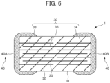
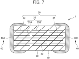
- the multilayer ceramic capacitor 1 may be a multilayer ceramic capacitor including a two-portion structure, a three-portion structure, or a four-portion structure as shown in FIGS. 6 , 7 , and 8 .
- the multilayer ceramic capacitor 1 shown in FIG. 6 is a multilayer ceramic capacitor 1 having a two-portion structure, and includes, as internal electrode layers 30, floating internal electrode layers 35 which are not exposed at either the first end surface LS1 or the second end surface LS2 in addition to the first internal electrode layers 33 and the second internal electrode layers 34.
- the multilayer ceramic capacitor 1 shown in FIG. 7 is a multilayer ceramic capacitor 1 having a three-portion structure including first floating internal electrode layers 35A and second floating internal electrode layers 35B as floating internal electrode layers 35.
- the multilayer ceramic capacitor 1 shown in FIG. 8 is a multilayer ceramic capacitor 1 having a four-portion structure including first floating internal electrode layers 35A, second floating internal electrode layers 35B, and third floating internal electrode layers 35C as floating internal electrode layers 35.
- the multilayer ceramic capacitor 1 has a structure in which the counter electrode portions are divided into a plurality of portions. With such a configuration, a plurality of capacitor components are provided between the opposing internal electrode layers 30, and these capacitor components are connected in series. Therefore, the voltages applied to the respective capacitor components are reduced, and thus it is possible to improve the pressure resistance of the multilayer ceramic capacitor 1.
- the multilayer ceramic capacitor 1 of the present embodiment may include a multiple-portion structure of four or more.
- the multilayer ceramic capacitor 1 may be of a two-terminal type including two external electrodes or of a multi-terminal type including a large number of external electrodes.
- the multilayer ceramic electronic component a multilayer ceramic capacitor in which the dielectric layers 20 made of dielectric ceramic are used as a ceramic layer is exemplified.
- the multilayer ceramic electronic component of the present disclosure is not limited thereto.
- the ceramic electronic component of the present disclosure can be applied to various multilayer ceramic electronic components such as a piezoelectric component using a piezoelectric ceramic as a ceramic layer, a thermistor using a semiconductor ceramic as a ceramic layer, and an inductor using a magnetic ceramic as a ceramic layer.
- Piezoelectric ceramic includes PZT (lead zirconate titanate) ceramic
- semiconductor ceramic includes spinel ceramic
- magnetic ceramic includes ferrite ceramic.
- the present invention is not limited to embodiments of the present invention, and can be appropriately modified and applied without departing from the gist of the present invention.
- the present invention also includes combinations of two or more of the individual desirable configurations described in the above embodiments.
Landscapes
- Engineering & Computer Science (AREA)
- Power Engineering (AREA)
- Microelectronics & Electronic Packaging (AREA)
- Manufacturing & Machinery (AREA)
- Chemical & Material Sciences (AREA)
- Ceramic Engineering (AREA)
- Inorganic Chemistry (AREA)
- Mechanical Engineering (AREA)
- Organic Chemistry (AREA)
- Metallurgy (AREA)
- Materials Engineering (AREA)
- Chemical Kinetics & Catalysis (AREA)
- Physics & Mathematics (AREA)
- Dispersion Chemistry (AREA)
- Spectroscopy & Molecular Physics (AREA)
- Fixed Capacitors And Capacitor Manufacturing Machines (AREA)
- Ceramic Capacitors (AREA)
Applications Claiming Priority (2)
| Application Number | Priority Date | Filing Date | Title |
|---|---|---|---|
| JP2022150525 | 2022-09-21 | ||
| PCT/JP2023/026360 WO2024062753A1 (ja) | 2022-09-21 | 2023-07-19 | 積層セラミック電子部品 |
Publications (1)
| Publication Number | Publication Date |
|---|---|
| EP4576139A1 true EP4576139A1 (en) | 2025-06-25 |
Family
ID=90454402
Family Applications (1)
| Application Number | Title | Priority Date | Filing Date |
|---|---|---|---|
| EP23867879.1A Pending EP4576139A1 (en) | 2022-09-21 | 2023-07-19 | Multilayer ceramic electronic component |
Country Status (6)
| Country | Link |
|---|---|
| US (1) | US20250054698A1 (https=) |
| EP (1) | EP4576139A1 (https=) |
| JP (1) | JPWO2024062753A1 (https=) |
| KR (1) | KR20250023559A (https=) |
| CN (1) | CN119404267A (https=) |
| WO (1) | WO2024062753A1 (https=) |
Family Cites Families (6)
| Publication number | Priority date | Publication date | Assignee | Title |
|---|---|---|---|---|
| JP2584643B2 (ja) | 1987-12-19 | 1997-02-26 | 富士通株式会社 | 熱処理装置 |
| JPH11162771A (ja) | 1997-11-25 | 1999-06-18 | Kyocera Corp | 積層セラミックコンデンサ |
| JP4106813B2 (ja) * | 1999-06-15 | 2008-06-25 | 三菱マテリアル株式会社 | チップ型電子部品 |
| JP2009267146A (ja) * | 2008-04-25 | 2009-11-12 | Murata Mfg Co Ltd | 積層セラミック電子部品 |
| JP2016009836A (ja) * | 2014-06-26 | 2016-01-18 | 株式会社村田製作所 | 積層セラミック電子部品 |
| JP2021125673A (ja) * | 2020-02-10 | 2021-08-30 | 株式会社村田製作所 | 積層セラミックコンデンサ |
-
2023
- 2023-07-19 JP JP2024548108A patent/JPWO2024062753A1/ja active Pending
- 2023-07-19 KR KR1020257001725A patent/KR20250023559A/ko active Pending
- 2023-07-19 CN CN202380051811.1A patent/CN119404267A/zh active Pending
- 2023-07-19 WO PCT/JP2023/026360 patent/WO2024062753A1/ja not_active Ceased
- 2023-07-19 EP EP23867879.1A patent/EP4576139A1/en active Pending
-
2024
- 2024-10-24 US US18/925,488 patent/US20250054698A1/en active Pending
Also Published As
| Publication number | Publication date |
|---|---|
| WO2024062753A1 (ja) | 2024-03-28 |
| US20250054698A1 (en) | 2025-02-13 |
| JPWO2024062753A1 (https=) | 2024-03-28 |
| KR20250023559A (ko) | 2025-02-18 |
| CN119404267A (zh) | 2025-02-07 |
Similar Documents
| Publication | Publication Date | Title |
|---|---|---|
| US10453612B2 (en) | Multilayer ceramic capacitor | |
| US11062848B2 (en) | Multilayer ceramic electronic component | |
| US11183334B2 (en) | Multilayer ceramic electronic component | |
| EP4439600A1 (en) | Multilayer ceramic electronic component | |
| CN115881434B (zh) | 层叠陶瓷电容器 | |
| CN116264131A (zh) | 层叠陶瓷电容器 | |
| US10395835B2 (en) | Multilayer ceramic electronic component | |
| US10269497B2 (en) | Electronic component | |
| US20240404760A1 (en) | Multilayer ceramic capacitor | |
| EP4576139A1 (en) | Multilayer ceramic electronic component | |
| EP4621819A1 (en) | Layered ceramic electronic component | |
| EP4589614A1 (en) | Multilayer ceramic electronic component | |
| US10395836B2 (en) | Multilayer ceramic electronic component | |
| US20220068560A1 (en) | Multilayer ceramic capacitor | |
| US20250299883A1 (en) | Multilayer ceramic electronic component | |
| US20250279243A1 (en) | Multilayer ceramic electronic component | |
| US20250299885A1 (en) | Multilayer ceramic electronic component | |
| US12525403B2 (en) | Multilayer ceramic electronic component | |
| US20250111995A1 (en) | Multilayer ceramic capacitor | |
| US20250029784A1 (en) | Multilayer ceramic electronic component | |
| US20250308793A1 (en) | Multilayer ceramic electronic component | |
| EP4651164A1 (en) | Multilayer ceramic capacitor | |
| US20250308795A1 (en) | Multilayer ceramic electronic component | |
| US20250299884A1 (en) | Multilayer ceramic capacitor | |
| KR20260053019A (ko) | 적층 세라믹 콘덴서 |
Legal Events
| Date | Code | Title | Description |
|---|---|---|---|
| STAA | Information on the status of an ep patent application or granted ep patent |
Free format text: STATUS: THE INTERNATIONAL PUBLICATION HAS BEEN MADE |
|
| PUAI | Public reference made under article 153(3) epc to a published international application that has entered the european phase |
Free format text: ORIGINAL CODE: 0009012 |
|
| STAA | Information on the status of an ep patent application or granted ep patent |
Free format text: STATUS: REQUEST FOR EXAMINATION WAS MADE |
|
| 17P | Request for examination filed |
Effective date: 20250319 |
|
| AK | Designated contracting states |
Kind code of ref document: A1 Designated state(s): AL AT BE BG CH CY CZ DE DK EE ES FI FR GB GR HR HU IE IS IT LI LT LU LV MC ME MK MT NL NO PL PT RO RS SE SI SK SM TR |
|
| DAV | Request for validation of the european patent (deleted) | ||
| DAX | Request for extension of the european patent (deleted) |