WO2024053084A1 - 半導体装置 - Google Patents
半導体装置 Download PDFInfo
- Publication number
- WO2024053084A1 WO2024053084A1 PCT/JP2022/033850 JP2022033850W WO2024053084A1 WO 2024053084 A1 WO2024053084 A1 WO 2024053084A1 JP 2022033850 W JP2022033850 W JP 2022033850W WO 2024053084 A1 WO2024053084 A1 WO 2024053084A1
- Authority
- WO
- WIPO (PCT)
- Prior art keywords
- conductor layer
- semiconductor device
- insulating substrate
- configuration
- view
- Prior art date
- Legal status (The legal status is an assumption and is not a legal conclusion. Google has not performed a legal analysis and makes no representation as to the accuracy of the status listed.)
- Ceased
Links
Images






Classifications
-
- H—ELECTRICITY
- H10—SEMICONDUCTOR DEVICES; ELECTRIC SOLID-STATE DEVICES NOT OTHERWISE PROVIDED FOR
- H10W—GENERIC PACKAGES, INTERCONNECTIONS, CONNECTORS OR OTHER CONSTRUCTIONAL DETAILS OF DEVICES COVERED BY CLASS H10
- H10W70/00—Package substrates; Interposers; Redistribution layers [RDL]
- H10W70/60—Insulating or insulated package substrates; Interposers; Redistribution layers
-
- H—ELECTRICITY
- H10—SEMICONDUCTOR DEVICES; ELECTRIC SOLID-STATE DEVICES NOT OTHERWISE PROVIDED FOR
- H10W—GENERIC PACKAGES, INTERCONNECTIONS, CONNECTORS OR OTHER CONSTRUCTIONAL DETAILS OF DEVICES COVERED BY CLASS H10
- H10W70/00—Package substrates; Interposers; Redistribution layers [RDL]
- H10W70/60—Insulating or insulated package substrates; Interposers; Redistribution layers
- H10W70/62—Insulating or insulated package substrates; Interposers; Redistribution layers characterised by their interconnections
- H10W70/65—Shapes or dispositions of interconnections
-
- H—ELECTRICITY
- H10—SEMICONDUCTOR DEVICES; ELECTRIC SOLID-STATE DEVICES NOT OTHERWISE PROVIDED FOR
- H10W—GENERIC PACKAGES, INTERCONNECTIONS, CONNECTORS OR OTHER CONSTRUCTIONAL DETAILS OF DEVICES COVERED BY CLASS H10
- H10W42/00—Arrangements for protection of devices
- H10W42/121—Arrangements for protection of devices protecting against mechanical damage
-
- H—ELECTRICITY
- H10—SEMICONDUCTOR DEVICES; ELECTRIC SOLID-STATE DEVICES NOT OTHERWISE PROVIDED FOR
- H10W—GENERIC PACKAGES, INTERCONNECTIONS, CONNECTORS OR OTHER CONSTRUCTIONAL DETAILS OF DEVICES COVERED BY CLASS H10
- H10W70/00—Package substrates; Interposers; Redistribution layers [RDL]
- H10W70/60—Insulating or insulated package substrates; Interposers; Redistribution layers
- H10W70/611—Insulating or insulated package substrates; Interposers; Redistribution layers for connecting multiple chips together
-
- H—ELECTRICITY
- H10—SEMICONDUCTOR DEVICES; ELECTRIC SOLID-STATE DEVICES NOT OTHERWISE PROVIDED FOR
- H10W—GENERIC PACKAGES, INTERCONNECTIONS, CONNECTORS OR OTHER CONSTRUCTIONAL DETAILS OF DEVICES COVERED BY CLASS H10
- H10W72/00—Interconnections or connectors in packages
- H10W72/50—Bond wires
-
- H—ELECTRICITY
- H10—SEMICONDUCTOR DEVICES; ELECTRIC SOLID-STATE DEVICES NOT OTHERWISE PROVIDED FOR
- H10W—GENERIC PACKAGES, INTERCONNECTIONS, CONNECTORS OR OTHER CONSTRUCTIONAL DETAILS OF DEVICES COVERED BY CLASS H10
- H10W74/00—Encapsulations, e.g. protective coatings
- H10W74/10—Encapsulations, e.g. protective coatings characterised by their shape or disposition
- H10W74/111—Encapsulations, e.g. protective coatings characterised by their shape or disposition the semiconductor body being completely enclosed
- H10W74/114—Encapsulations, e.g. protective coatings characterised by their shape or disposition the semiconductor body being completely enclosed by a substrate and the encapsulations
-
- H—ELECTRICITY
- H10—SEMICONDUCTOR DEVICES; ELECTRIC SOLID-STATE DEVICES NOT OTHERWISE PROVIDED FOR
- H10W—GENERIC PACKAGES, INTERCONNECTIONS, CONNECTORS OR OTHER CONSTRUCTIONAL DETAILS OF DEVICES COVERED BY CLASS H10
- H10W40/00—Arrangements for thermal protection or thermal control
- H10W40/20—Arrangements for cooling
- H10W40/25—Arrangements for cooling characterised by their materials
- H10W40/255—Arrangements for cooling characterised by their materials having a laminate or multilayered structure, e.g. direct bond copper [DBC] ceramic substrates
-
- H—ELECTRICITY
- H10—SEMICONDUCTOR DEVICES; ELECTRIC SOLID-STATE DEVICES NOT OTHERWISE PROVIDED FOR
- H10W—GENERIC PACKAGES, INTERCONNECTIONS, CONNECTORS OR OTHER CONSTRUCTIONAL DETAILS OF DEVICES COVERED BY CLASS H10
- H10W72/00—Interconnections or connectors in packages
- H10W72/071—Connecting or disconnecting
- H10W72/075—Connecting or disconnecting of bond wires
-
- H—ELECTRICITY
- H10—SEMICONDUCTOR DEVICES; ELECTRIC SOLID-STATE DEVICES NOT OTHERWISE PROVIDED FOR
- H10W—GENERIC PACKAGES, INTERCONNECTIONS, CONNECTORS OR OTHER CONSTRUCTIONAL DETAILS OF DEVICES COVERED BY CLASS H10
- H10W90/00—Package configurations
Definitions
- the present disclosure relates to a semiconductor device.
- a semiconductor device has been proposed in which a slight undercut shape is provided by etching or pressing on the side surface of a circuit pattern that is a single conductor layer (for example, Patent Document 1). According to such a configuration, the anchor effect due to the undercut shape makes it possible to suppress peeling of the sealing member due to temperature changes or the like.
- the present disclosure has been made in view of the above problems, and aims to provide a technique that can more reliably suppress peeling of the sealing member.
- a semiconductor device includes: an insulating substrate; a first conductor layer bonded on the insulating substrate; a second conductor layer having an overhang portion that is a side end projecting in the lateral direction; a sealing member having a portion embedded in a space between the overhang portion and the insulating substrate; and a semiconductor element covered with a stopper member.
- the second conductor layer has an overhang portion that is a side end portion that protrudes laterally than the side end portion of the first conductor layer, and the sealing member has the overhang portion and the overhang portion. It has a part buried in the space between it and the insulating substrate. According to such a configuration, peeling of the sealing member can be more reliably suppressed.
- FIG. 1 is a cross-sectional view showing the configuration of a semiconductor device according to Embodiment 1.
- FIG. FIG. 3 is a cross-sectional view showing the configuration of a semiconductor device according to a second embodiment.
- FIG. 3 is a cross-sectional view showing the configuration of a semiconductor device according to a third embodiment.
- FIG. 4 is a cross-sectional view showing the configuration of a semiconductor device according to a fourth embodiment.
- FIG. 7 is a cross-sectional view showing the configuration of a semiconductor device according to a fifth embodiment.
- FIG. 7 is a cross-sectional view showing the configuration of a semiconductor device according to a sixth embodiment. 7 is a cross-sectional view showing the configuration of a semiconductor device according to Embodiment 7.
- FIG. FIG. FIG. 3 is a cross-sectional view showing the configuration of a semiconductor device according to a second embodiment.
- FIG. 3 is a cross-sectional view showing the configuration of a semiconductor device according to a third embodiment.
- FIG. 7 is a top view showing the configuration of a semiconductor device according to a seventh embodiment.
- FIG. 7 is a cross-sectional view showing the configuration of a semiconductor device according to an eighth embodiment.
- 12 is a cross-sectional view showing the configuration of a semiconductor device according to a ninth embodiment.
- FIG. 9 is a top view showing the configuration of a semiconductor device according to a ninth embodiment.
- 10 is a cross-sectional view showing the configuration of a semiconductor device according to a tenth embodiment.
- FIG. 1 is a cross-sectional view showing the configuration of a semiconductor device 100 according to the first embodiment.
- the semiconductor device 100 includes a ceramic insulating substrate 1, a first conductor layer 2, a second conductor layer 3, a semiconductor element 5, a solder 6, a wire 7, a third conductor layer 8, and a base portion. 9 and a sealing member 10.
- the ceramic insulating substrate 1 is an insulating substrate made of, for example, aluminum nitride (AlN) or silicon nitride (SiN).
- the first conductor layer 2 is bonded on the ceramic insulating substrate 1 , that is, on the surface of the ceramic insulating substrate 1
- the third conductor layer 8 is bonded under the ceramic insulating substrate 1 , that is, on the back surface of the ceramic insulating substrate 1 . There is.
- the first conductor layer 2 and the third conductor layer 8 have a plurality of circuit patterns. After the first conductor layer 2 is bonded to the ceramic insulating substrate 1, a circuit pattern may be formed on the first conductor layer 2 by etching or the like, or a circuit pattern may be formed on the first conductor layer 2 by pressing or the like. After that, the first conductor layer 2 may be bonded to the ceramic insulating substrate 1.
- the formation of the circuit pattern of the third conductor layer 8 is similar to the formation of the circuit pattern of the first conductor layer 2.
- the second conductor layer 3 is bonded onto the first conductor layer 2, that is, to the surface of the first conductor layer 2.
- the second conductor layer 3 has an overhang portion 3a that is a side end portion that protrudes laterally (in a direction corresponding to the left-right direction in FIG. 1) than the side end portion of the first conductor layer 2.
- the overhang portion 3a protrudes laterally from the side end portion of the first conductor layer 2 by, for example, about 50 ⁇ m.
- An undercut shape is formed by the side portion of the first conductor layer 2 and the overhang portion 3a of the second conductor layer 3.
- the second conductor layer 3 may be patterned as appropriate so as to maintain the wiring relationship based on the circuit pattern of the first conductor layer 2.
- the material of the first conductor layer 2 and the second conductor layer 3 is, for example, aluminum containing an alloy or copper.
- the material of the first conductor layer 2 is aluminum and the material of the second conductor layer 3 is copper, it is expected that the heat dissipation of the semiconductor device 100 will be improved, and the semiconductor device will have improved rigidity. 100 can be expected to improve reliability.
- the material of the third conductor layer 8 may be the same as the material of the first conductor layer 2.
- brazing, soldering, welding, liquid phase or solid phase diffusion bonding, or the like may be used, for example.
- the semiconductor element 5 is electrically connected to the second conductor layer 3.
- the semiconductor element 5 is bonded to the surface of the second conductor layer 3 with solder 6.
- the semiconductor element 5 is, for example, a MOSFET (Metal Oxide Semiconductor Field Effect Transistor), an IGBT (Insulated Gate Bipolar Transistor), an RC-IGBT (Reverse Conducting - IGBT), an SBD (Schottky Barrier Diode), or a PND (PN junction diode).
- the material of the semiconductor element 5 may be ordinary silicon (Si), or may be a wide bandgap semiconductor such as silicon carbide (SiC), gallium nitride (GaN), or diamond. When the material of the semiconductor element 5 is a wide bandgap semiconductor, stable operation under high temperature and high voltage and high switching speed are possible.
- the semiconductor element 5 is electrically connected to other circuit patterns (not shown) by wires 7.
- the material of the wire 7 is, for example, aluminum.
- the semiconductor element 5 may be electrically connected to other circuit patterns by a bus bar (not shown) instead of the wire 7.
- other circuit patterns may be electrically connected to the external terminals by, for example, soldering or welding.
- the base portion 9 is bonded below the third conductive layer 8.
- the base portion 9 is made of aluminum or copper, for example, and is a cooling member such as a pin fin or a base plate.
- the sealing member 10 covers the semiconductor element 5.
- the sealing member 10 also covers the first conductor layer 2, the second conductor layer 3, and the like.
- the material of the sealing member 10 is, for example, resin such as epoxy or gel, and the sealing member 10 is formed by transfer molding. Note that the sealing member 10 is also filled under the overhang portion 3a. That is, the sealing member 10 has a portion embedded in the space 4 between the overhang portion 3a and the ceramic insulating substrate 1.
- the temperature of a semiconductor device changes depending on the current supply operation or the external environment. If the sealing member 10 peels off from the ceramic insulating substrate 1, the first conductor layer 2, the second conductor layer 3, the semiconductor element 5, etc. due to this temperature change, the reliability of the semiconductor device may decrease. There is.
- the second conductive layer 3 has an overhang that is a side end portion that protrudes laterally beyond the side end portion of the first conductive layer 2.
- the sealing member 10 has a portion embedded in the space 4 between the overhang portion 3a and the ceramic insulating substrate 1. According to such a configuration, peeling of the sealing member 10 in the vertical direction can be suppressed due to the anchor effect of the overhang portion 3a.
- the size of the second conductor layer 3 in the lateral direction slightly larger than the size of the first conductor layer 2 in the lateral direction, the length by which the overhang portion 3a protrudes can be stabilized. can. Therefore, the undercut shape can be stabilized regardless of the thickness of the first conductor layer 2, etc., so that the effect of suppressing peeling of the sealing member can be obtained more reliably. Further, in a configuration in which multiple sets of the first conductor layer 2 and the second conductor layer 3 are provided, insulation between each set can be ensured by simply ensuring the distance between the second conductor layers 3. Therefore, it becomes easy to ensure insulation.
- the length of the overhang portion 3a protruding beyond the side end portion of the first conductor layer 2 is approximately 50 ⁇ m
- the size of the semiconductor device 100 in the lateral direction may be somewhat larger. If so, the length may be 50 ⁇ m or more.
- FIG. 2 is a cross-sectional view showing the configuration of the semiconductor device 100 according to the second embodiment.
- the configuration in FIG. 2 is similar to the configuration in FIG. 1 with the fourth conductor layer 11 added.
- the fourth conductor layer 11 is bonded below the third conductor layer 8 in the same way that the second conductor layer 3 is bonded onto the first conductor layer 2 .
- the rigidity of the fourth conductive layer 11 is different from the rigidity of the third conductive layer 8.
- the difference in rigidity between the first conductor layer 2 and the third conductor layer 8 makes the ceramic insulating substrate Warpage occurs in 1.
- the material of the first conductor layer 2 is pure aluminum and the material of the second conductor layer 3 is a copper alloy, relatively large warpage occurs in the ceramic insulating substrate 1.
- the fourth conductor layer 11 having a different rigidity from the third conductor layer 8 is bonded under the third conductor layer 8.
- the rigidity of the third conductor layer 8 and the fourth conductor layer 11 can improve the balance between the upper and lower rigidities of the ceramic insulating substrate 1, thereby suppressing warping of the ceramic insulating substrate 1. can do. This can be expected to improve the reliability and ease of assembly of the semiconductor device 100.
- FIG. 3 is a cross-sectional view showing the configuration of semiconductor device 100 according to the third embodiment. Note that illustration of the sealing member 10 is omitted from FIG. 3 onwards.
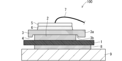
- the configuration in FIG. 3 is similar to the configuration in FIG. 1 in which a recess 3b is provided in the second conductor layer 3.
- the recess 3b of the second conductor layer 3 is slightly larger than the upper part, which is a part of the first conductor layer 2, and fits into the upper part of the first conductor layer 2.
- the second conductor layer 3 is bonded onto the first conductor layer 2.
- the recess 3b is formed in the second conductor layer 3 by, for example, pressing or machining.
- the second conductor layer 3 is provided with the recess 3b that fits into a part of the first conductor layer 2. According to such a configuration, when the first conductor layer 2 and the second conductor layer 3 are bonded together, the positioning of the first conductor layer 2 and the second conductor layer 3 becomes easy, and their positioning becomes easy. Since the deviation can be reduced, the length by which the overhang portion 3a projects can be stabilized. Further, in a configuration in which multiple sets of the first conductor layer 2 and the second conductor layer 3 are provided, it is possible to stabilize the distance between the second conductor layers 3, that is, the distance between each pair. Therefore, the insulation can be stabilized. Moreover, a decrease in the rigidity of the first conductor layer 2 can be suppressed.
- the shape of the recess 3b in plan view may be a polygon such as a rectangle or a hexagon, or may be circular.
- the shape of the recess 3b in plan view is polygonal, rotation of one of the first conductor layer 2 and the second conductor layer 3 with respect to the other can be suppressed.
- FIG. 4 is a cross-sectional view showing the configuration of semiconductor device 100 according to the fourth embodiment.
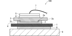
- the configuration in FIG. 4 is similar to the configuration in FIG. 1 in which the second conductor layer 3 is provided with a convex portion 3c and the first conductor layer 2 is provided with a concave portion 2a.
- the convex portion 3c is provided at the lower center of the second conductor layer 3.
- the recess 2a of the first conductor layer 2 is slightly larger than the convex part 3c, which is a part of the second conductor layer 3, and fits into the convex part 3c of the second conductor layer 3. In this state, the second conductor layer 3 is bonded onto the first conductor layer 2.
- the recess 2a is formed in the first conductor layer 2 by, for example, pressing or machining.
- the recess 2a may be formed before the first conductor layer 2 is bonded to the ceramic insulating substrate 1, or may be formed after the first conductor layer 2 is bonded to the ceramic insulating substrate 1.
- the convex portion 3c is formed on the second conductor layer 3 by, for example, pressing or machining.
- the first conductor layer 2 is provided with the recess 2a that fits into a part of the second conductor layer 3. According to such a configuration, the same effects as in the third embodiment can be obtained.
- the shape of the recess 2a in plan view may be a polygon such as a rectangle or a hexagon, or may be circular.
- the shape of the recess 2a in plan view is polygonal, rotation of one of the first conductor layer 2 and the second conductor layer 3 with respect to the other can be suppressed.
- FIG. 5 is a cross-sectional view showing the configuration of a semiconductor device 100 according to the fifth embodiment.
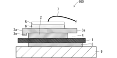
- the configuration in FIG. 5 is similar to the configuration in FIG. 1 in which a recessed and relatively thin stepped portion 2b is provided on the outer peripheral portion of the first conductor layer 2 in a cross-sectional view.
- the stepped portion 2b is provided at the outer periphery of the upper surface of the first conductor layer 2 on the second conductor layer 3 side.
- the step portion 2b is formed in the first conductor layer 2 by, for example, pressing or machining.
- the step portion 2b may be formed before or after the first conductor layer 2 is bonded to the ceramic insulating substrate 1.
- the depth of the stepped portion 2b may be half or less of the thickness of the first conductor layer 2, for example, by half-cutting.
- the width of the stepped portion 2b is, for example, 50 ⁇ m or more and 5 mm or less.
- the thickness of the first conductor layer 2 may be, for example, about 0.1 mm to 2 mm, or smaller than 0.1 mm. However, when the thickness of the first conductive layer 2 becomes smaller than 0.1 mm, the space 4 between the overhang portion 3a and the ceramic insulating substrate 1 becomes smaller, so that the sealing member 10 is not filled in the space 4. It becomes difficult.
- the recessed step portion 2b is provided at the outer peripheral portion of the first conductive layer 2. According to such a configuration, the size of the space 4 between the overhang portion 3a and the ceramic insulating substrate 1 can be ensured, so that filling the sealing member 10 into the space 4 becomes easy. Furthermore, even if the projecting length of the overhang portion 3a cannot be increased due to miniaturization of the semiconductor device 100, a sealing member may be provided in the space between the second conductive layer 3 and the stepped portion 2b. 10, an anchor effect is obtained. Therefore, it is possible to achieve both miniaturization and improved reliability of the semiconductor device 100.
- FIG. 6 is a cross-sectional view showing the configuration of a semiconductor device 100 according to the sixth embodiment.
- the configuration in FIG. 6 is similar to the configuration in FIG. 1 in which a recessed and relatively thin stepped portion 3d is provided on the outer peripheral portion of the second conductive layer 3 in a cross-sectional view.
- the stepped portion 3d is provided at the outer periphery of the lower surface of the second conductor layer 3 on the first conductor layer 2 side.
- the step portion 3d is formed in the second conductor layer 3 by, for example, pressing or machining.
- the formation, depth, and dimensions of the stepped portion 3d are the same as, for example, the formation, depth, and dimensions of the stepped portion 2b according to the fifth embodiment.
- the recessed step portion 3d is provided at the outer peripheral portion of the surface of the second conductor layer 3 on the first conductor layer 2 side. According to such a configuration, the same effects as in the fifth embodiment can be obtained.
- Embodiment 5 and Embodiment 6 may be combined. That is, the first conductor layer 2 may be provided with the step portion 2b, and the second conductor layer 3 may be provided with the step portion 3d.
- FIG. 7 is a cross-sectional view showing the structure of a semiconductor device 100 according to the seventh embodiment
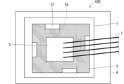
- FIG. 8 is a top view showing the structure of the semiconductor device 100.
- the convex portion 3e is located further back than the second conductor layer 3 other than the convex portion 3e, and is therefore illustrated with a hidden dotted line.
- FIGS. 7 and 8 differ from the configuration shown in FIG. 1 in that the overhang portion 3a is provided with a convex portion 3e that protrudes toward the ceramic insulating substrate 1, and the outer peripheral portion of the overhang portion 3a in plan view is
- the structure is similar to that in which a notch portion 3f is provided.
- the convex portion 3e can be formed by providing a notch at both ends of a portion of each side of the second conductive layer 3 by machining, laser cutting, or pressing, and then bending the portion downward by, for example, a press. It is formed. As shown in FIG. 8, a cutout portion 3f is formed in the portion of the second conductor layer 3 used for the convex portion 3e. Note that the formation of the convex portion 3e and the notch portion 3f is not limited to this.
- the width of the notch 3f in the direction along each side of the second conductor layer 3 is, for example, 1 mm to 10 mm, and the depth of the notch 3f is, for example, 0.2 mm to 2 mm.
- the angle at which the protrusion 3e projects from the second conductor layer 3 other than the protrusion 3e is, for example, 45° to 135°, and the height of the protrusion 3e is smaller than the thickness of the first conductor layer 2.
- the convex portion 3e that protrudes toward the ceramic insulating substrate 1 is provided on the overhang portion 3a. According to such a configuration, when the first conductor layer 2 and the second conductor layer 3 are bonded together, the positioning of the first conductor layer 2 and the second conductor layer 3 becomes easy, and their positioning becomes easy. Since the deviation can be reduced, the length by which the overhang portion 3a projects can be stabilized.
- a cutout portion 3f is provided at the outer peripheral portion of the overhang portion 3a in plan view. According to such a configuration, the anchor effect obtained by filling the notch portion 3f with the sealing member 10 can suppress lateral peeling of the sealing member 10.
- FIG. 9 is a cross-sectional view showing the configuration of a semiconductor device 100 according to the eighth embodiment.
- the configuration of FIG. 9 is a plurality of portions of the configuration of FIG. 1 in which the second conductor layer 3 is laminated in the thickness direction of the second conductor layer 3 (direction corresponding to the vertical direction in FIG. 9). This is similar to the configuration including layers 3g, 3h, and 3i.
- the side end portion of the partial layer far from the first conductive layer 2 among the plurality of partial layers 3g to 3i is the side end portion of the partial layer close to the first conductive layer 2 among the plurality of partial layers 3g to 3i. It protrudes laterally.
- the material or thickness of the plurality of partial layers 3g to 3i does not need to be the same, and may be changed as necessary. Further, the number of the plurality of partial layers included in the second conductor layer 3 is not limited to three.
- the first conductor layer 2 includes a plurality of partial layers 3g to 3i, and the side ends of the partial layers far from the first conductor layer 2 are , protrudes in the lateral direction from the side edge of the partial layer near the first conductor layer 2.
- the path to the space 4 between the overhang portion 3a and the ceramic insulating substrate 1 can be widened, making it easier to fill the space 4 with the sealing member 10 during manufacturing.
- the semiconductor elements 5 have various sizes and there is a margin in the bonding area, the size of the space 4 can be increased while ensuring the distance and insulation between the circuit patterns.
- any one of the partial layers 3g to 3i is made of aluminum and the remaining one is made of copper, warping of the semiconductor device 100 can be suppressed.
- FIG. 10 is a cross-sectional view showing the structure of a semiconductor device 100 according to the ninth embodiment
- FIG. 11 is a top view showing the structure of the semiconductor device 100.
- the configurations in FIGS. 10 and 11 are similar to the configuration in FIG. 1 in which a through hole 3j is provided in the overhang portion 3a along the thickness direction of the second conductor layer 3.
- the diameter of the through hole 3j is, for example, 80% or more of the thickness of the second conductive layer 3, and is formed by machining or press working.
- the through hole 3j is provided in the overhang portion 3a along the thickness direction of the second conductor layer 3. According to such a configuration, the anchor effect obtained by filling the through hole 3j with the sealing member 10 can suppress lateral peeling of the sealing member 10. Further, during manufacturing, the sealing member 10 easily flows into the space 4 under the overhang portion 3a through the through hole 3j, so that the sealing member 10 can be easily filled into the space 4.
- FIG. 12 is a cross-sectional view showing the configuration of a semiconductor device 100 according to the tenth embodiment.
- the configuration in FIG. 12 is similar to the configuration in FIG. 1 in which the corner portion 3k of the overhang portion 3a in cross-sectional view has an acute angle.
- a corner 3k formed by the upper surface and side surface of the overhang portion 3a is an acute angle.
- the corner portion 3k is formed, for example, by machining or pressing, and the internal angle of the corner portion 3k is, for example, 45° or less.
- the corner portion 3k of the overhang portion 3a has an acute angle in a cross-sectional view. According to such a configuration, even if a crack should occur, the sharp corner 3k can intentionally cause the crack to grow in a direction with less influence on the semiconductor device 100.
- the direction with less influence on the semiconductor device 100 is, for example, the direction away from the semiconductor element 5. This makes it possible to control the propagation direction of cracks, thereby suppressing deterioration in the life and reliability of the semiconductor device 100.
Landscapes
- Cooling Or The Like Of Semiconductors Or Solid State Devices (AREA)
- Structures Or Materials For Encapsulating Or Coating Semiconductor Devices Or Solid State Devices (AREA)
- Engineering & Computer Science (AREA)
- Microelectronics & Electronic Packaging (AREA)
- Physics & Mathematics (AREA)
- Geometry (AREA)
Priority Applications (5)
| Application Number | Priority Date | Filing Date | Title |
|---|---|---|---|
| US18/872,205 US20250329659A1 (en) | 2022-09-09 | 2022-09-09 | Semiconductor device |
| PCT/JP2022/033850 WO2024053084A1 (ja) | 2022-09-09 | 2022-09-09 | 半導体装置 |
| DE112022007753.0T DE112022007753B4 (de) | 2022-09-09 | 2022-09-09 | Halbleitervorrichtung |
| CN202280099542.1A CN119768912A (zh) | 2022-09-09 | 2022-09-09 | 半导体装置 |
| JP2024545394A JP7802187B2 (ja) | 2022-09-09 | 2022-09-09 | 半導体装置 |
Applications Claiming Priority (1)
| Application Number | Priority Date | Filing Date | Title |
|---|---|---|---|
| PCT/JP2022/033850 WO2024053084A1 (ja) | 2022-09-09 | 2022-09-09 | 半導体装置 |
Publications (1)
| Publication Number | Publication Date |
|---|---|
| WO2024053084A1 true WO2024053084A1 (ja) | 2024-03-14 |
Family
ID=90192474
Family Applications (1)
| Application Number | Title | Priority Date | Filing Date |
|---|---|---|---|
| PCT/JP2022/033850 Ceased WO2024053084A1 (ja) | 2022-09-09 | 2022-09-09 | 半導体装置 |
Country Status (5)
| Country | Link |
|---|---|
| US (1) | US20250329659A1 (https=) |
| JP (1) | JP7802187B2 (https=) |
| CN (1) | CN119768912A (https=) |
| DE (1) | DE112022007753B4 (https=) |
| WO (1) | WO2024053084A1 (https=) |
Citations (7)
| Publication number | Priority date | Publication date | Assignee | Title |
|---|---|---|---|---|
| JP2002064168A (ja) * | 2000-08-17 | 2002-02-28 | Toshiba Eng Co Ltd | 冷却装置、冷却装置の製造方法および半導体装置 |
| JP2011029420A (ja) * | 2009-07-27 | 2011-02-10 | Nichia Corp | 光半導体装置及びその製造方法 |
| JP2015046416A (ja) * | 2013-08-27 | 2015-03-12 | 三菱電機株式会社 | 半導体装置および半導体装置の製造方法 |
| JP6210818B2 (ja) * | 2013-09-30 | 2017-10-11 | 三菱電機株式会社 | 半導体装置およびその製造方法 |
| JP2018067669A (ja) * | 2016-10-20 | 2018-04-26 | トレックス・セミコンダクター株式会社 | 半導体装置の製造方法および半導体装置 |
| JP2018129442A (ja) * | 2017-02-09 | 2018-08-16 | エイブリック株式会社 | 半導体装置およびその製造方法 |
| WO2022145310A1 (ja) * | 2020-12-29 | 2022-07-07 | 三菱電機株式会社 | 半導体装置の製造方法、半導体装置用基板の製造方法、半導体装置及び電力変換装置 |
Family Cites Families (5)
| Publication number | Priority date | Publication date | Assignee | Title |
|---|---|---|---|---|
| JP4334054B2 (ja) * | 1999-03-26 | 2009-09-16 | 株式会社東芝 | セラミックス回路基板 |
| JP5860599B2 (ja) | 2011-03-01 | 2016-02-16 | 昭和電工株式会社 | 絶縁回路基板、パワーモジュール用ベースおよびその製造方法 |
| JP6201490B2 (ja) | 2013-07-30 | 2017-09-27 | 株式会社豊田自動織機 | 半導体装置 |
| JP6607105B2 (ja) | 2016-03-22 | 2019-11-20 | 三菱マテリアル株式会社 | 回路基板及び半導体モジュール、回路基板の製造方法 |
| JP7176397B2 (ja) * | 2018-12-21 | 2022-11-22 | 株式会社デンソー | 半導体装置とその製造方法 |
-
2022
- 2022-09-09 US US18/872,205 patent/US20250329659A1/en active Pending
- 2022-09-09 CN CN202280099542.1A patent/CN119768912A/zh active Pending
- 2022-09-09 WO PCT/JP2022/033850 patent/WO2024053084A1/ja not_active Ceased
- 2022-09-09 JP JP2024545394A patent/JP7802187B2/ja active Active
- 2022-09-09 DE DE112022007753.0T patent/DE112022007753B4/de active Active
Patent Citations (7)
| Publication number | Priority date | Publication date | Assignee | Title |
|---|---|---|---|---|
| JP2002064168A (ja) * | 2000-08-17 | 2002-02-28 | Toshiba Eng Co Ltd | 冷却装置、冷却装置の製造方法および半導体装置 |
| JP2011029420A (ja) * | 2009-07-27 | 2011-02-10 | Nichia Corp | 光半導体装置及びその製造方法 |
| JP2015046416A (ja) * | 2013-08-27 | 2015-03-12 | 三菱電機株式会社 | 半導体装置および半導体装置の製造方法 |
| JP6210818B2 (ja) * | 2013-09-30 | 2017-10-11 | 三菱電機株式会社 | 半導体装置およびその製造方法 |
| JP2018067669A (ja) * | 2016-10-20 | 2018-04-26 | トレックス・セミコンダクター株式会社 | 半導体装置の製造方法および半導体装置 |
| JP2018129442A (ja) * | 2017-02-09 | 2018-08-16 | エイブリック株式会社 | 半導体装置およびその製造方法 |
| WO2022145310A1 (ja) * | 2020-12-29 | 2022-07-07 | 三菱電機株式会社 | 半導体装置の製造方法、半導体装置用基板の製造方法、半導体装置及び電力変換装置 |
Also Published As
| Publication number | Publication date |
|---|---|
| US20250329659A1 (en) | 2025-10-23 |
| JPWO2024053084A1 (https=) | 2024-03-14 |
| JP7802187B2 (ja) | 2026-01-19 |
| DE112022007753T5 (de) | 2025-06-18 |
| DE112022007753B4 (de) | 2026-01-22 |
| CN119768912A (zh) | 2025-04-04 |
Similar Documents
| Publication | Publication Date | Title |
|---|---|---|
| US8350369B2 (en) | High power semiconductor package | |
| US8129225B2 (en) | Method of manufacturing an integrated circuit module | |
| US20160365296A1 (en) | Electronic Devices with Increased Creepage Distances | |
| JP2014216459A (ja) | 半導体装置 | |
| JP7540248B2 (ja) | 半導体モジュール | |
| CN113451244A (zh) | 双面散热的mosfet封装结构及其制造方法 | |
| US20160021780A1 (en) | Carrier, Semiconductor Module and Fabrication Method Thereof | |
| WO2013172139A1 (ja) | 半導体デバイス | |
| CN112447671B (zh) | 具有倾斜的接触表面和凸起的桥的互连夹具 | |
| JP2015167171A (ja) | 半導体装置 | |
| WO2024053084A1 (ja) | 半導体装置 | |
| WO2019116910A1 (ja) | 半導体装置および半導体装置の製造方法 | |
| JP6546496B2 (ja) | 半導体パワーモジュール | |
| US20240258372A1 (en) | Electronic component and package including stress release structure as lateral edge portion of semiconductor body | |
| US20160113123A1 (en) | Method for Soldering a Circuit Carrier to a Carrier Plate | |
| US9355999B2 (en) | Semiconductor device | |
| JP2011176206A (ja) | 半導体装置およびその製造方法 | |
| JP2018116960A (ja) | 電力用半導体装置 | |
| TWI489601B (zh) | 電子元件封裝結構 | |
| US20210074667A1 (en) | Interconnect Clip with Angled Contact Surface and Raised Bridge Technical Field | |
| JP2022064488A (ja) | 半導体部品 | |
| JP7136367B2 (ja) | 半導体パッケージ | |
| JP7484766B2 (ja) | 半導体モジュール | |
| CN110416178A (zh) | 一种集成电路封装结构及其封装方法 | |
| JP7802763B2 (ja) | 半導体装置 |
Legal Events
| Date | Code | Title | Description |
|---|---|---|---|
| 121 | Ep: the epo has been informed by wipo that ep was designated in this application |
Ref document number: 22958162 Country of ref document: EP Kind code of ref document: A1 |
|
| ENP | Entry into the national phase |
Ref document number: 2024545394 Country of ref document: JP Kind code of ref document: A |
|
| WWE | Wipo information: entry into national phase |
Ref document number: 18872205 Country of ref document: US |
|
| WWE | Wipo information: entry into national phase |
Ref document number: 202280099542.1 Country of ref document: CN |
|
| WWP | Wipo information: published in national office |
Ref document number: 202280099542.1 Country of ref document: CN |
|
| WWE | Wipo information: entry into national phase |
Ref document number: 112022007753 Country of ref document: DE |
|
| WWP | Wipo information: published in national office |
Ref document number: 112022007753 Country of ref document: DE |
|
| 122 | Ep: pct application non-entry in european phase |
Ref document number: 22958162 Country of ref document: EP Kind code of ref document: A1 |
|
| WWP | Wipo information: published in national office |
Ref document number: 18872205 Country of ref document: US |
|
| WWG | Wipo information: grant in national office |
Ref document number: 112022007753 Country of ref document: DE |