WO2024047991A1 - スイッチ駆動装置、インバータ回路 - Google Patents
スイッチ駆動装置、インバータ回路 Download PDFInfo
- Publication number
- WO2024047991A1 WO2024047991A1 PCT/JP2023/020984 JP2023020984W WO2024047991A1 WO 2024047991 A1 WO2024047991 A1 WO 2024047991A1 JP 2023020984 W JP2023020984 W JP 2023020984W WO 2024047991 A1 WO2024047991 A1 WO 2024047991A1
- Authority
- WO
- WIPO (PCT)
- Prior art keywords
- switch
- signal
- control signal
- detection
- voltage
- Prior art date
- Legal status (The legal status is an assumption and is not a legal conclusion. Google has not performed a legal analysis and makes no representation as to the accuracy of the status listed.)
- Ceased
Links
Images







Classifications
-
- H—ELECTRICITY
- H02—GENERATION; CONVERSION OR DISTRIBUTION OF ELECTRIC POWER
- H02M—APPARATUS FOR CONVERSION BETWEEN AC AND AC, BETWEEN AC AND DC, OR BETWEEN DC AND DC, AND FOR USE WITH MAINS OR SIMILAR POWER SUPPLY SYSTEMS; CONVERSION OF DC OR AC INPUT POWER INTO SURGE OUTPUT POWER; CONTROL OR REGULATION THEREOF
- H02M1/00—Details of apparatus for conversion
- H02M1/08—Circuits specially adapted for the generation of control voltages for semiconductor devices incorporated in static converters
-
- H—ELECTRICITY
- H02—GENERATION; CONVERSION OR DISTRIBUTION OF ELECTRIC POWER
- H02M—APPARATUS FOR CONVERSION BETWEEN AC AND AC, BETWEEN AC AND DC, OR BETWEEN DC AND DC, AND FOR USE WITH MAINS OR SIMILAR POWER SUPPLY SYSTEMS; CONVERSION OF DC OR AC INPUT POWER INTO SURGE OUTPUT POWER; CONTROL OR REGULATION THEREOF
- H02M1/00—Details of apparatus for conversion
- H02M1/38—Means for preventing simultaneous conduction of switches
-
- H—ELECTRICITY
- H02—GENERATION; CONVERSION OR DISTRIBUTION OF ELECTRIC POWER
- H02M—APPARATUS FOR CONVERSION BETWEEN AC AND AC, BETWEEN AC AND DC, OR BETWEEN DC AND DC, AND FOR USE WITH MAINS OR SIMILAR POWER SUPPLY SYSTEMS; CONVERSION OF DC OR AC INPUT POWER INTO SURGE OUTPUT POWER; CONTROL OR REGULATION THEREOF
- H02M7/00—Conversion of AC power input into DC power output; Conversion of DC power input into AC power output
- H02M7/42—Conversion of DC power input into AC power output without possibility of reversal
- H02M7/44—Conversion of DC power input into AC power output without possibility of reversal by static converters
- H02M7/48—Conversion of DC power input into AC power output without possibility of reversal by static converters using discharge tubes with control electrode or semiconductor devices with control electrode
-
- H—ELECTRICITY
- H03—ELECTRONIC CIRCUITRY
- H03K—PULSE TECHNIQUE
- H03K17/00—Electronic switching or gating, i.e. not by contact-making and –breaking
- H03K17/16—Modifications for eliminating interference voltages or currents
-
- H—ELECTRICITY
- H03—ELECTRONIC CIRCUITRY
- H03K—PULSE TECHNIQUE
- H03K17/00—Electronic switching or gating, i.e. not by contact-making and –breaking
- H03K17/51—Electronic switching or gating, i.e. not by contact-making and –breaking characterised by the components used
- H03K17/56—Electronic switching or gating, i.e. not by contact-making and –breaking characterised by the components used by the use, as active elements, of semiconductor devices
- H03K17/687—Electronic switching or gating, i.e. not by contact-making and –breaking characterised by the components used by the use, as active elements, of semiconductor devices the devices being field-effect transistors
-
- Y—GENERAL TAGGING OF NEW TECHNOLOGICAL DEVELOPMENTS; GENERAL TAGGING OF CROSS-SECTIONAL TECHNOLOGIES SPANNING OVER SEVERAL SECTIONS OF THE IPC; TECHNICAL SUBJECTS COVERED BY FORMER USPC CROSS-REFERENCE ART COLLECTIONS [XRACs] AND DIGESTS
- Y02—TECHNOLOGIES OR APPLICATIONS FOR MITIGATION OR ADAPTATION AGAINST CLIMATE CHANGE
- Y02B—CLIMATE CHANGE MITIGATION TECHNOLOGIES RELATED TO BUILDINGS, e.g. HOUSING, HOUSE APPLIANCES OR RELATED END-USER APPLICATIONS
- Y02B70/00—Technologies for an efficient end-user side electric power management and consumption
- Y02B70/10—Technologies improving the efficiency by using switched-mode power supplies [SMPS], i.e. efficient power electronics conversion e.g. power factor correction or reduction of losses in power supplies or efficient standby modes
Definitions
- the present disclosure relates to a switch drive device and an inverter circuit using the same.
- Patent Document 1 can be mentioned as an example of the conventional technology related to the above.
- the switch driving device disclosed herein includes an upper driver configured to receive an input of an upper control signal and output an upper drive signal to turn on/off an upper switch of a power circuit.
- a lower driver configured to receive a lower control signal and output a lower drive signal to turn on/off a lower switch of the power circuit; and the upper control signal is at an off logic level.
- the switch voltage appearing at the connection node between the upper switch and the lower switch has fallen, the switch current flowing through the upper switch has fallen, or the upper drive signal has reached an off logic level.
- a first detection circuit configured to generate a first detection signal by detecting that the first detection signal has been switched to the lower side control signal; a first control circuit configured to switch to an on logic level.
- FIG. 1 is a diagram showing an example of the configuration of an inverter circuit.
- FIG. 2 is a diagram showing a general method for setting dead time.
- FIG. 3 is a diagram showing an example of the configuration of a power circuit.
- FIG. 4 is a diagram showing an example of a module configuration.
- FIG. 5 is a diagram showing an equivalent circuit of the module as seen from the switch driving device.
- FIG. 6 is a diagram illustrating a new dead time setting method (for example, under heavy load).
- FIG. 7 is a diagram showing a new dead time setting method (for example, when the load is light).
- FIG. 8 is a diagram showing a first embodiment (outline) of a switch driving device.
- FIG. 9 is a diagram showing a first embodiment (simplified) of the switch driving device.
- FIG. 1 is a diagram showing an example of the configuration of an inverter circuit.
- FIG. 2 is a diagram showing a general method for setting dead time.
- FIG. 3 is a
- FIG. 10 is a diagram showing the first embodiment (details) of the switch driving device.
- FIG. 11 is a diagram showing the dead time setting operation in the first embodiment.
- FIG. 12 is a diagram showing a second embodiment (outline) of the switch driving device.
- FIG. 13 is a diagram showing a second embodiment (simplified) of the switch driving device.
- FIG. 14 is a diagram showing the second embodiment (details) of the switch driving device.
- FIG. 15 is a diagram showing the dead time setting operation in the second embodiment.
- FIG. 16 is a diagram showing a third embodiment (outline) of a switch driving device.
- FIG. 17 is a diagram showing a third embodiment (simplified) of the switch driving device.
- FIG. 18 is a diagram showing the third embodiment (details) of the switch driving device.
- FIG. 19 is a diagram showing the dead time setting operation in the third embodiment.
- FIG. 1 is a diagram showing an example of the configuration of an inverter circuit.
- the inverter circuit 1 of this configuration example is a type of power converter that receives input of DC power from a DC power supply 2 and outputs AC power to a load 3.
- the inverter circuit 1 includes a switch drive device 100 and a power circuit 200.
- the switch driving device 100 is a semiconductor device (so-called gate driver IC [integrated circuit]) for driving the power circuit 200.
- the power circuit 200 receives a gate drive signal from the switch drive device 100 and outputs AC power to the load 3.
- power circuit 200 includes transistors Q1 to Q4.
- Transistors Q1-Q4 may be SiC devices, for example.
- the drain of the transistor Q1 is connected to the positive terminal of the DC power supply 2.
- the source of transistor Q1 is connected to the first end of load 3.
- the gate of transistor Q1 is connected to switch driving device 100.
- Transistor Q1 connected in this way functions as the upper switch of the first phase forming a full-bridge output stage.
- the drain of the transistor Q2 is connected to the first end of the load 3.
- the source of transistor Q2 is connected to the negative terminal (ground terminal) of DC power supply 2.
- the gate of transistor Q2 is connected to switch driving device 100.
- Transistor Q2 connected in this way functions as the lower switch of the first phase forming a full-bridge output stage.
- the drain of the transistor Q3 is connected to the positive terminal of the DC power supply 2.
- the source of transistor Q3 is connected to the second end of load 3.
- the gate of transistor Q3 is connected to switch driver 100.
- Transistor Q3 connected in this way functions as the upper switch of the second phase forming a full-bridge output stage.
- the drain of the transistor Q4 is connected to the second end of the load 3.
- the source of transistor Q4 is connected to the negative terminal (ground terminal) of DC power supply 2.
- the gate of transistor Q4 is connected to switch driving device 100.
- Transistor Q4 connected in this way functions as the lower switch of the second phase forming a full-bridge output stage.
- body diodes D1 to D4 are attached to the transistors Q1 to Q4, respectively, with the drains of the transistors Q1 to Q4 serving as cathodes, and the sources of the transistors Q1 to Q4 serving as anodes.
- the load 3 connected to the inverter circuit 1 is an inductive load (such as a motor coil)
- the normal current increases due to the induced electromotive force of the load 3 immediately after all of the transistors Q1 to Q4 are turned off.
- a return current may flow in the opposite direction.
- transistors Q1 and Q4 are both in an on state, and transistors Q2 and Q3 are both in an off state.
- a normal current flows through a current path L1 from the positive end of the DC power supply 2 to the negative end of the DC power supply 2 via the transistor Q1, the load 3, and the transistor Q4.
- FIG. 2 is a diagram showing a general method of setting dead time DT.
- the gate-source voltage Vgs (Q1) of the transistor Q1, the drain-source current Ids (Q1) of the transistor Q1, the drain-source voltage Vds (Q1) of the transistor Q1, and The gate-source voltage Vgs(Q2) of transistor Q2 is depicted.
- the measurement of the dead time DT is started at the timing when the dead time DT starts to decrease.
- the gate-source voltage Vgs (Q1) of the transistor Q1 has not fallen below the plateau voltage Vp. Therefore, transistor Q1 still remains on. That is, the drain-source current Ids(Q1) of the transistor Q1 continues to flow as before time t101. Further, the drain-source voltage Vds (Q1) of the transistor Q1 is maintained at approximately 0V.
- the gate-source voltage Vgs (Q1) of the transistor Q1 has a slow falling speed during the transition from the high level to the low level (near the plateau voltage Vp). Therefore, if the above dead time DT is short, as shown at time t103, the gate-source voltage Vgs(Q2) of the transistor Q2 increases before the drain-source current Ids(Q1) of the transistor Q1 reaches 0A. The plateau voltage Vp is reached. As a result, both transistors Q1 and Q2 are turned on, so that an excessive through current may flow.
- FIG. 3 is a diagram showing an example of the configuration of the power circuit 200.
- Power circuit 200 of this configuration example includes modules 210 and 220.
- the module 210 includes the aforementioned transistors Q1 and Q2 and forms the first phase of a full-bridge output stage.
- Module 220 includes the aforementioned transistors Q3 and Q4 and forms the second phase of the full-bridge output stage.
- the transistor Q1 includes three unit transistors Q1a, Q1b, and Q1c connected in parallel between the positive end of the DC power supply 2 and the first end of the load 3.
- Body diodes D1a, D1b and D1c are associated with unit transistors Q1a, Q1b and Q1c, respectively.
- the transistor Q2 includes three unit transistors Q2a, Q2b, and Q2c connected in parallel between the first end of the load 3 and the negative end of the DC power supply 2.
- Body diodes D2a, D2b and D2c are associated with unit transistors Q2a, Q2b and Q2c, respectively.
- Transistor Q3 includes three unit transistors Q3a, Q3b, and Q3c connected in parallel between the positive end of DC power supply 2 and the second end of load 3.
- Body diodes D3a, D3b and D3c are associated with unit transistors Q3a, Q3b and Q3c, respectively.
- Transistor Q4 includes three unit transistors Q4a, Q4b, and Q4c connected in parallel between the second end of load 3 and the negative end of DC power supply 2.
- Body diodes D4a, D4b and D4c are associated with unit transistors Q4a, Q4b and Q4c, respectively.
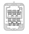
- FIG. 4 is a diagram showing an example of the configuration of the module 210.
- the unit transistors Q1a to Q1c and Q2a to Q2c have connections between their respective source pads and the metal frame, between their respective gate pads and the metal frame, and between their respective source pads. , a large number of wires are bonded.
- the module 220 has the same configuration as the module 210. Therefore, the module 220 can be understood by replacing the unit transistors Q1a to Q1c and Q2a to Q2c in the figure with unit transistors Q3a to Q3c and Q4a to Q4c, respectively.
- FIG. 5 is a diagram showing an equivalent circuit of the module 210 (or 220) as seen from the switch driving device 100.
- the module 210 when viewed from the switch driving device 100, the module 210 includes a gate resistor Rg and N unit transistors (according to FIGS. 3 and 4, three unit transistors Q1a to Q1c or Q2a to Q2c) can be understood as an RC time constant circuit formed by the respective input capacitance Ciss.
- the freewheeling current can only flow through the module 210 for a short time (for example, 500 ns)
- the dead time DT described above is set to a short time (for example, 2 ⁇ s)
- the transistors Q1 and Q2 The risk of simultaneous on-on will increase.
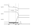
- ⁇ Dead time setting method (new)> 6 and 7 are diagrams each showing a new method of setting the dead time DT.
- the gate-source voltage Vgs (Q1) of the transistor Q1 the gate-source voltage Vgs (Q1) of the transistor Q1, the drain-source current Ids (Q1) of the transistor Q1, and the drain-source voltage Vds (Q1) of the transistor Q1 are shown. Each is depicted.
- FIG. 6 shows behavior under heavy load, for example.
- the gate-source voltage Vgs (Q1) of transistor Q1 begins to decrease from high level to low level. However, at this point, the gate-source voltage Vgs (Q1) of the transistor Q1 has not fallen below the plateau voltage Vp. Therefore, transistor Q1 still remains on. In other words, the drain-source current Ids(Q1) of the transistor Q1 continues to flow as before time t201. Further, the drain-source voltage Vds (Q1) of the transistor Q1 is maintained at approximately 0V.
- time measurement of delay time Td (for example, 500 ns) is started.
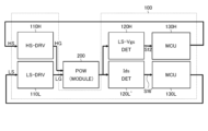
- FIG. 8 is a diagram showing a first embodiment (outline) of the switch driving device 100. In particular, this figure depicts functional blocks of the switch driving device 100 in the first embodiment.
- the switch driving device 100 of this embodiment includes an upper driver 110H, a lower driver 110L, detection circuits 120L and 120H, and control circuits 130L and 130H.
- the upper driver 110H receives the upper control signal HS from the control circuit 130H and amplifies it to generate the upper drive signal HG. Then, the upper driver 110H outputs the upper drive signal HG to the power circuit 200 to turn on/off the transistor Q1 (or the transistor Q3, hereinafter the same) of the power circuit 200.
- the lower driver 110L receives the lower control signal LS from the control circuit 130L and amplifies it to generate the lower drive signal LG. Then, the lower driver 110L outputs the lower drive signal LG to the power circuit 200 to turn on/off the transistor Q2 (or the transistor Q4, hereinafter the same) of the power circuit 200.
- the detection circuit 120L detects that the switch voltage Vsw appearing at the connection node between the transistor Q1 and the transistor Q2 falls, and generates the detection signal S16.
- the fall of the switch voltage Vsw can be understood as a fall of the drain-source voltage Vds (Q2) of the transistor Q2 or a rise of the drain-source voltage Vds (Q1) of the transistor Q1.
- fall of the lower drive signal LG can be understood as the fall of the gate-source voltage Vgs (Q2) of the transistor Q2.
- FIG. 9 is a diagram showing a first embodiment (simplified) of the switch driving device 100. In particular, this figure simply depicts the internal configuration of some of the functional blocks in FIG. 8 mentioned earlier.
- the upper driver 110H receives the upper control signal HS from the control circuit 130H and outputs the upper drive signal HG to the gate of the transistor Q1.
- the transistor Q1 is turned on when the upper drive signal HG is at a high level, and is turned off when the upper drive signal HG is at a low level.
- the lower driver 110L receives the lower control signal LS from the control circuit 130L and outputs the lower drive signal LG to the gate of the transistor Q2.
- the transistor Q2 is turned on when the lower drive signal LG is at a high level, and turned off when the lower drive signal LG is at a low level.
- the detection circuit 120L monitors the switch voltage Vsw to detect the fall of the drain-source voltage Vds (Q2) of the transistor Q2 (and the rise of the drain-source voltage Vds (Q1) of the transistor Q1). A detection signal S16 is generated.
- the detection circuit 120H generates the detection signal S12 by monitoring the lower drive signal LG and detecting the fall of the gate-source voltage Vgs (Q2) of the transistor Q2.
- the control circuit 130L receives the detection signal S16 from the detection circuit 120L and outputs the lower control signal LS to the lower driver 110L.
- the control circuit 130L includes a control section 131L, a delay section 132L, and an AND gate 133L.
- the AND gate 133L (corresponding to the first calculation section) performs an AND operation on the control signal S15 and the delay signal S17 to generate an AND signal S18.
- the AND signal S18 becomes a high level when both the control signal S15 and the delay signal S17 are at a high level, and becomes a low level when at least one of the control signal S15 and the delay signal S17 is at a low level.
- the AND signal S18 is output to the lower driver 110L as the lower control signal LS.
- the control circuit 130H receives the detection signal S12 from the detection circuit 120H and outputs the upper control signal HS to the upper driver 110H.
- the control circuit 130H includes a control section 131H, a delay section 132H, and an AND gate 133H.
- the delay time Td2 may be the same value as the delay time Td1 (for example, 500 ns).
- the AND gate 133H (corresponding to a second calculation unit) performs a logical product operation on the control signal S11 and the delayed signal S13 to generate a logical product signal S14.
- the AND signal S14 becomes high level when both the control signal S11 and the delayed signal S13 are high level, and becomes low level when at least one of the control signal S11 and the delayed signal S13 is low level.
- the AND signal S14 is output to the upper driver 110H as the upper control signal HS.
- FIG. 10 is a diagram showing the first embodiment (details) of the switch driving device 100.
- this figure depicts in detail the internal configuration of the functional blocks in FIGS. 8 and 9 previously mentioned.
- the detection circuit 120H includes a comparator CMP1.
- Comparator CMP1 generates a detection signal S12 by comparing the lower drive signal LG input to the inverting input terminal (-) and a predetermined threshold voltage V11 input to the non-inverting input terminal (+). . Therefore, the detection signal S12 becomes a low level when the lower drive signal LG is higher than the threshold voltage V11, and becomes a high level when the lower drive signal LG is lower than the threshold voltage V11.
- the threshold voltage V11 is set to an appropriate value so that the comparator CMP1 is unlikely to malfunction. For example, when the lower drive signal LG is pulse-driven between 5V and 0V, the threshold voltage V11 may be set to 2V.
- the detection circuit 120L includes resistors R1 and R2 and a comparator CMP2.
- the first end of the resistor R1 is connected to the application end of the switch voltage Vsw.
- the second end of the resistor R1 and the first end of the resistor R2 are both connected to the application end of the divided voltage V12.
- a second end of the resistor R2 is connected to a ground terminal.
- the comparator CMP2 generates the detection signal S16 by comparing the divided voltage V12 input to the inverting input terminal (-) and the threshold voltage V13 input to the non-inverting input terminal (+). Therefore, the detection signal S16 becomes a low level when the divided voltage V12 is higher than the threshold voltage V13, and becomes a high level when the divided voltage V12 is lower than the threshold voltage V13.
- the logic level of the detection signal S16 is switched at the timing when the switch voltage Vsw falls below VDD/2 (for example, 200 to 400 V) with respect to the power supply voltage VDD (for example, 400 to 800 V) applied to the positive terminal of the DC power supply 2.
- VDD/2 for example, 200 to 400 V
- VDD for example, 400 to 800 V
- the voltage division ratio of the divided voltage V12 and the threshold voltage V13 may be set.
- the threshold voltage V13 is set to an appropriate value so that the comparator CMP2 is unlikely to malfunction. For example, when the power supply voltage VDD is 400V and the voltage division ratio of the divided voltage V12 is 1/400, the threshold voltage V13 may be set to 0.5V.
- the control circuit 130 is a functional block that includes the previously mentioned control circuits 130L and 130H. Referring to the figure, the control circuit 130 includes a control section 131, delay sections 132L and 132H, AND gates 133L and 133H, and NOR gates 134 and 135.
- the control circuit 130 may be, for example, an MCU (micro controller unit).
- the control unit 131 is a functional unit that includes the previously mentioned control units 131L and 131H. Referring to the figure, the control section 131 includes a delay section 131a, an AND gate 131b, and a NOR gate 131c.
- the delay unit 131a delays the reference control signal S1 to generate a delayed control signal S2.
- the AND gate 131b performs an AND operation on the reference control signal S1 and the delayed control signal S2 to generate the previously mentioned control signal S11. Therefore, the control signal S11 is at a high level when both the reference control signal S1 and the delayed control signal S2 are at a high level, and is at a low level when at least one of the reference control signal S1 and the delayed control signal S2 is at a low level. becomes.
- the NOR gate 131c performs a NOR operation on the reference control signal S1 and the delayed control signal S2 to generate the previously mentioned control signal S15. Therefore, the control signal S15 is at a high level when both the reference control signal S1 and the delayed control signal S2 are at a low level, and is at a low level when at least one of the reference control signal S1 and the delayed control signal S2 is at a high level. becomes.
- the delay unit 132L delays the detection signal S16 by a delay time Td1 (for example, 500 ns) to generate a delayed signal S17.
- Td1 for example, 500 ns
- the delay unit 132H generates a delayed signal S13 by delaying the detection signal S12 (latch detection signal S19 in this figure) by a delay time Td2 (for example, 500 ns).
- the first input terminal of the NOR gate 134 is connected to the application terminal of the detection signal S12.
- the second input terminal of the NOR gate 134 and the output terminal of the NOR gate 135 are both connected to the application terminal of the latch detection signal S19.
- a first input terminal of NOR gate 135 is connected to an output terminal of NOR gate 134.
- a second input terminal of the NOR gate 135 is connected to an application terminal of the control signal S15.
- the NOR gates 134 and 135 connected in this way function as an RS flip-flop that generates the latch detection signal S19 according to the detection signal S12 and the control signal S15.
- the latch detection signal S19 is set to a high level at a pulse edge of the detection signal S12, and reset to a low level at a pulse edge of the control signal S15. Therefore, protection is applied so that the high levels of the detection signal S12 and the control signal S15 do not overlap.
- the upper driver 110H receives the upper control signal HS and outputs the upper drive signal HG.
- a gate resistor RgH may be connected between the output end of the upper driver 110H and the gate of the transistor Q1.
- the lower driver 110L receives the lower control signal LS and outputs the lower drive signal LG.
- a gate resistor RgL may be connected between the output end of the lower driver 110L and the gate of the transistor Q2.
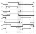
- FIG. 11 is a diagram showing the dead time setting operation in the first embodiment.
- the control signal S11, the detection signal S12, the delayed signal S13, the AND signal S14, the control signal S15, the detection signal S16, the delayed signal S17, and the AND signal S18 are depicted in order from the top.
- the lower drive signal LG falls below the plateau voltage Vp and further below the threshold voltage V11.
- the detection signal S12 rises to high level.
- the delay signal S13 is maintained at a low level until a delay time Td2 (for example, 500 ns) elapses after the detection signal S12 rises to a high level.
- the detection signal S12 falls to a low level at time t5
- the delayed signal S13 falls to a low level at a time t8 after a delay time Td2.
- the AND signal S14 also falls to a low level without delay.
- the detection signal S16 rises to high level.
- the delay signal S17 is maintained at a low level until a delay time Td1 (for example, 500 ns) has elapsed after the detection signal S16 rises to a high level.
- the detection signal S16 falls to a low level at time t10
- the delayed signal S17 falls to a low level at time t12 after a delay time Td1.
- the control signal S15 falls to a low level
- the AND signal S18 also falls to a low level without delay.
- transistors Q1 and Q2 simultaneously Hard to turn on. Therefore, generation of excessive through current is prevented.
- FIG. 12 is a diagram showing a second embodiment (outline) of the switch driving device 100.
- the switch driving device 100 of this embodiment is based on the first embodiment (FIG. 8) described above, but includes a detection circuit 120L' in place of the detection circuit 120L.
- the detection circuit 120L' detects that the transistor Q1 actually transitions to the off state after the upper control signal HS is switched to low level, and generates the detection signal S16'.
- the detection circuit 120L' detects that the switch current flowing through the transistor Q1, that is, the drain-source current Ids (Q1) of the transistor Q1 falls, and generates the detection signal S16'.
- FIG. 13 is a diagram showing a second embodiment (simplified) of the switch driving device 100.
- the detection circuit 120L' is connected between the sources of the transistors Q2 and Q4 and the ground terminal, and detects the fall of the drain-source current Ids (Q4) of the transistor Q4. , and in turn, detects the fall of the drain-source current Ids (Q1) of the transistor Q1 to generate a detection signal S16'.
- FIG. 14 is a diagram showing the second embodiment (details) of the switch driving device 100.
- this figure depicts in detail the internal configuration of the functional blocks in FIGS. 12 and 13 mentioned above.
- a capacitor 4 may be connected between the positive and negative ends of the DC power supply 2.
- the detection circuit 120L' includes a resistor R3, an amplifier AMP1, and a comparator CMP3.
- the first end of the resistor R3 is connected to the source of the transistor Q2.
- the non-inverting input terminal (+) of the amplifier AMP1 is connected to the first terminal of the resistor R3.
- the inverting input terminal (-) of the amplifier AMP1 is connected to the second terminal of the resistor R3.
- the amplifier AMP1 connected in this way amplifies the detection voltage V21 appearing across the resistor R3 to generate an amplified voltage V22.
- the comparator CMP3 compares the amplified voltage V22 input to the inverting input terminal (-) and the threshold voltage V23 input to the non-inverting input terminal (+) to generate a detection signal S16'. Therefore, the detection signal S16' becomes low level when the amplified voltage V22 is higher than the threshold voltage V23, and becomes high level when the amplified voltage V22 is lower than the threshold voltage V23.
- FIG. 15 is a diagram showing the dead time setting operation in the second embodiment.
- the control signal S11, the detection signal S12, the delayed signal S13, the AND signal S14, the control signal S15, the detection signal S16', the delayed signal S17, and the AND signal S18 are depicted in order from the top. .
- the content of this figure is the same as that of the first embodiment (FIG. 11) described earlier, except that the detection signal S16 is replaced with the detection signal S16'. Focusing on the difference from the first embodiment (FIG. 11), at time t7, when the off time ⁇ 1 of the transistor Q1 has elapsed, the upper drive signal HG (not shown) falls below the plateau voltage Vp. Therefore, the drain-source current Ids (Q1) of the transistor Q1 falls, and the detection voltage V22 falls below the threshold voltage V23. As a result, the detection signal S16' rises to high level.
- transistors Q1 and Q2 simultaneously Hard to turn on. Therefore, generation of excessive through current is prevented.
- FIG. 16 is a diagram showing a third embodiment (outline) of the switch driving device 100.
- the switch driving device 100 of this embodiment is based on the first embodiment (FIG. 8) described above, but includes a detection circuit 120L'' in place of the detection circuit 120L.
- the detection circuit 120L'' detects that the transistor Q1 actually transitions to the off state after the upper control signal HS is switched to low level, and generates the detection signal S16''.
- the fall of the upper drive signal HG can be understood as the fall of the gate-source voltage Vgs (Q1) of the transistor Q1.
- FIG. 17 is a diagram showing a third embodiment (simplified) of the switch driving device 100.
- the detection circuit 120L'' generates the detection signal S16'' by monitoring the upper drive signal HG and detecting the fall of the gate-source voltage Vgs (Q1) of the transistor Q1. do.
- FIG. 18 is a diagram showing the third embodiment (details) of the switch driving device 100. In particular, this figure depicts in detail the internal configuration of the functional blocks in FIGS. 16 and 17.
- the detection circuit 120L'' includes an amplifier AMP2 and a comparator CMP4.
- the comparator CMP4 compares the amplified voltage V31 input to the inverting input terminal (-) and the threshold voltage V32 input to the non-inverting input terminal (+) to generate a detection signal S16''. Therefore, the detection signal S16'' becomes a low level when the amplified voltage V31 is higher than the threshold voltage V32, and becomes a high level when the amplified voltage V31 is lower than the threshold voltage V32.
- Control circuit 130 includes NOR gates 136 and 137 in addition to the aforementioned components 131-135.
- the first input terminal of the NOR gate 136 is connected to the application terminal of the detection signal S16''.
- the second input terminal of the NOR gate 136 and the output terminal of the NOR gate 137 are both connected to the application terminal of the latch detection signal S20.
- a first input terminal of the NOR gate 137 is connected to an output terminal of the NOR gate 136.
- a second input terminal of the NOR gate 137 is connected to an application terminal of the control signal S11.
- the NOR gates 136 and 137 connected in this manner function as an RS flip-flop that generates the latch detection signal S20 in response to the detection signal S16'' and the control signal S11.
- the latch detection signal S20 is " is set to high level at the pulse edge of control signal S11, and reset to low level at the pulse edge of control signal S11. Therefore, protection is applied so that the high levels of the detection signal S16'' and the control signal S11 do not overlap.
- FIG. 19 is a diagram showing the dead time setting operation in the third embodiment.
- the control signal S11, detection signal S12, delay signal S13, AND signal S14, control signal S15, detection signal S16'', delay signal S17, and AND signal S18 are depicted in order from the top. .
- transistors Q1 and Q2 simultaneously Hard to turn on. Therefore, generation of excessive through current is prevented.
- the switch driving device disclosed herein includes an upper driver configured to receive an input of an upper control signal and output an upper drive signal to turn on/off an upper switch of a power circuit.
- a lower driver configured to receive a lower control signal and output a lower drive signal to turn on/off a lower switch of the power circuit; and the upper control signal is at an off logic level.
- the switch voltage appearing at the connection node between the upper switch and the lower switch has fallen, the switch current flowing through the upper switch has fallen, or the upper drive signal has reached an off logic level.
- a first detection circuit configured to generate a first detection signal by detecting that the first detection signal has been switched to the lower side control signal;
- a first control circuit configured to switch to an on logic level (first configuration).
- the first detection circuit has a configuration (a second detection circuit) that generates the first detection signal by comparing the switch voltage or its divided voltage with a predetermined threshold voltage. configuration).
- the first detection circuit generates the first detection signal by comparing a detection voltage corresponding to the switch current or an amplified voltage thereof with a predetermined threshold voltage.
- configuration (third configuration).
- the first detection circuit compares a differential voltage between the upper drive signal and the switch voltage or an amplified voltage thereof with a predetermined threshold voltage to detect the first detection circuit.
- a configuration (fourth configuration) that generates a signal may also be used.
- the first control circuit includes a first control section configured to generate a first control signal, and a first control section configured to generate a first control signal; a first delay unit configured to generate a first delayed signal by delaying by a first delay time; and a first delay unit configured to perform a logical operation on the first control signal and the first delayed signal to generate the lower control signal.
- the switch driving device detecting that the lower drive signal is switched to the off logic level after the lower control signal is switched to the off logic level; a second detection circuit configured to generate a second detection signal; and configured to switch the upper control signal to an on logic level after at least a second delay time has elapsed using the second detection signal as a trigger.
- the configuration may further include a second control circuit (sixth configuration).
- the second detection circuit has a configuration (seventh configuration) that generates the second detection signal by comparing the lower drive signal with a predetermined threshold voltage. It's okay.
- the second control circuit includes a second control section configured to generate a second control signal, and a second control section configured to generate a second control signal, and a second control section configured to generate a second control signal; a second delay unit configured to generate a second delayed signal by delaying by a time; and configured to perform a logical operation on the second control signal and the second delayed signal to generate the upper control signal.
- a configuration (eighth configuration) including a second calculation section may also be adopted.
- the inverter circuit disclosed in this specification has a configuration (ninth configuration) including the switch driving device according to any of the first to eighth configurations described above and the power circuit.
- the power circuit may be configured as a module including the upper switch and the lower switch (a tenth configuration).
- the upper switch and the lower switch may each include a plurality of unit transistors connected in parallel (an eleventh configuration).
- the upper switch and the lower switch may each be a SiC device (twelfth configuration).
Landscapes
- Engineering & Computer Science (AREA)
- Power Engineering (AREA)
- Inverter Devices (AREA)
Priority Applications (1)
| Application Number | Priority Date | Filing Date | Title |
|---|---|---|---|
| JP2024543795A JPWO2024047991A1 (https=) | 2022-09-01 | 2023-06-06 |
Applications Claiming Priority (2)
| Application Number | Priority Date | Filing Date | Title |
|---|---|---|---|
| JP2022139104 | 2022-09-01 | ||
| JP2022-139104 | 2022-09-01 |
Publications (1)
| Publication Number | Publication Date |
|---|---|
| WO2024047991A1 true WO2024047991A1 (ja) | 2024-03-07 |
Family
ID=90099239
Family Applications (1)
| Application Number | Title | Priority Date | Filing Date |
|---|---|---|---|
| PCT/JP2023/020984 Ceased WO2024047991A1 (ja) | 2022-09-01 | 2023-06-06 | スイッチ駆動装置、インバータ回路 |
Country Status (2)
| Country | Link |
|---|---|
| JP (1) | JPWO2024047991A1 (https=) |
| WO (1) | WO2024047991A1 (https=) |
Cited By (1)
| Publication number | Priority date | Publication date | Assignee | Title |
|---|---|---|---|---|
| WO2026040541A1 (zh) * | 2024-08-22 | 2026-02-26 | 圣邦微电子(北京)股份有限公司 | 低边开关驱动电路和低边驱动芯片 |
Citations (4)
| Publication number | Priority date | Publication date | Assignee | Title |
|---|---|---|---|---|
| JP2002204581A (ja) * | 2001-01-09 | 2002-07-19 | Fuji Electric Co Ltd | 電力用半導体モジュール |
| JP2005217774A (ja) * | 2004-01-29 | 2005-08-11 | Fujitsu Ten Ltd | スイッチング回路 |
| WO2018116458A1 (ja) * | 2016-12-22 | 2018-06-28 | 三菱電機株式会社 | 半導体装置、インバータおよび自動車 |
| US20190319617A1 (en) * | 2018-04-11 | 2019-10-17 | Stmicroelectronics S.R.L. | Drive circuit for half-bridges, corresponding driver, device and method |
-
2023
- 2023-06-06 JP JP2024543795A patent/JPWO2024047991A1/ja active Pending
- 2023-06-06 WO PCT/JP2023/020984 patent/WO2024047991A1/ja not_active Ceased
Patent Citations (4)
| Publication number | Priority date | Publication date | Assignee | Title |
|---|---|---|---|---|
| JP2002204581A (ja) * | 2001-01-09 | 2002-07-19 | Fuji Electric Co Ltd | 電力用半導体モジュール |
| JP2005217774A (ja) * | 2004-01-29 | 2005-08-11 | Fujitsu Ten Ltd | スイッチング回路 |
| WO2018116458A1 (ja) * | 2016-12-22 | 2018-06-28 | 三菱電機株式会社 | 半導体装置、インバータおよび自動車 |
| US20190319617A1 (en) * | 2018-04-11 | 2019-10-17 | Stmicroelectronics S.R.L. | Drive circuit for half-bridges, corresponding driver, device and method |
Cited By (1)
| Publication number | Priority date | Publication date | Assignee | Title |
|---|---|---|---|---|
| WO2026040541A1 (zh) * | 2024-08-22 | 2026-02-26 | 圣邦微电子(北京)股份有限公司 | 低边开关驱动电路和低边驱动芯片 |
Also Published As
| Publication number | Publication date |
|---|---|
| JPWO2024047991A1 (https=) | 2024-03-07 |
Similar Documents
| Publication | Publication Date | Title |
|---|---|---|
| US6275399B1 (en) | Method and apparatus for driving a semiconductor element with variable resistance circuitry | |
| US7479771B2 (en) | Current detection circuit and switching power supply | |
| JP6787348B2 (ja) | 半導体素子の過電流保護装置 | |
| JP2020036530A (ja) | スイッチング素子の駆動制御装置 | |
| US20100141304A1 (en) | Drive circuit for power element | |
| JPH0670540A (ja) | 電流制限出力を有するシステム及び電源回路 | |
| CN113504446A (zh) | 被配置为检测故障的电路及检测故障的方法 | |
| CN108377095B (zh) | 振铃振幅调整电路及方法 | |
| JP2019110486A (ja) | 半導体素子の電流検出回路及び電流検出方法 | |
| WO2020021757A1 (ja) | スイッチ回路及び電力変換装置 | |
| CN1638224B (zh) | 半导体器件和半导体器件模块 | |
| JP5282492B2 (ja) | スイッチング素子駆動回路 | |
| US20070262797A1 (en) | Driver circuit | |
| JP4360310B2 (ja) | 駆動装置 | |
| CN114667681A (zh) | 栅极驱动电路 | |
| JP6823485B2 (ja) | Dc/dcコンバータおよびその制御回路、車載電装機器 | |
| WO2024047991A1 (ja) | スイッチ駆動装置、インバータ回路 | |
| JPH06178552A (ja) | パワーデバイスの制御回路、レベルシフト回路及び半導体集積回路装置 | |
| EP0921624A1 (en) | Device for driving self arc-extinguishing type power element | |
| DE102021101327A1 (de) | Gate-ansteuerungsvorrichtung, gate-ansteuerungsverfahren, leistungshalbleitermodul und stromwandlervorrichtung | |
| JP2803444B2 (ja) | パワーデバイスの駆動保護回路 | |
| JP7671860B2 (ja) | ゲート制御パワースイッチにおけるショートに対する高速ショート検出のため方法および装置 | |
| JP4967568B2 (ja) | 電圧駆動型素子のゲート駆動回路 | |
| JP2001025259A (ja) | Pwmインバーター装置 | |
| JP2002208847A (ja) | 電力用半導体素子のゲート駆動回路 |
Legal Events
| Date | Code | Title | Description |
|---|---|---|---|
| 121 | Ep: the epo has been informed by wipo that ep was designated in this application |
Ref document number: 23859761 Country of ref document: EP Kind code of ref document: A1 |
|
| WWE | Wipo information: entry into national phase |
Ref document number: 2024543795 Country of ref document: JP |
|
| NENP | Non-entry into the national phase |
Ref country code: DE |
|
| 122 | Ep: pct application non-entry in european phase |
Ref document number: 23859761 Country of ref document: EP Kind code of ref document: A1 |