WO2024047991A1 - Switch drive device and inverter circuit - Google Patents
Switch drive device and inverter circuit Download PDFInfo
- Publication number
- WO2024047991A1 WO2024047991A1 PCT/JP2023/020984 JP2023020984W WO2024047991A1 WO 2024047991 A1 WO2024047991 A1 WO 2024047991A1 JP 2023020984 W JP2023020984 W JP 2023020984W WO 2024047991 A1 WO2024047991 A1 WO 2024047991A1
- Authority
- WO
- WIPO (PCT)
- Prior art keywords
- switch
- signal
- control signal
- detection
- voltage
- Prior art date
Links
- 238000001514 detection method Methods 0.000 claims abstract description 138
- 238000004364 calculation method Methods 0.000 claims description 6
- 238000010586 diagram Methods 0.000 description 37
- 230000003111 delayed effect Effects 0.000 description 28
- 238000000034 method Methods 0.000 description 13
- 230000007704 transition Effects 0.000 description 9
- 239000013643 reference control Substances 0.000 description 7
- 101710170230 Antimicrobial peptide 1 Proteins 0.000 description 5
- 101100464782 Saccharomyces cerevisiae (strain ATCC 204508 / S288c) CMP2 gene Proteins 0.000 description 5
- 101100464779 Saccharomyces cerevisiae (strain ATCC 204508 / S288c) CNA1 gene Proteins 0.000 description 4
- 230000001934 delay Effects 0.000 description 4
- 238000005259 measurement Methods 0.000 description 4
- 101710170231 Antimicrobial peptide 2 Proteins 0.000 description 3
- 230000008859 change Effects 0.000 description 3
- 239000003990 capacitor Substances 0.000 description 2
- 238000007429 general method Methods 0.000 description 2
- 230000007257 malfunction Effects 0.000 description 2
- 239000002184 metal Substances 0.000 description 2
- 238000012544 monitoring process Methods 0.000 description 2
- 230000002265 prevention Effects 0.000 description 2
- 238000012545 processing Methods 0.000 description 2
- 230000000295 complement effect Effects 0.000 description 1
- 238000005516 engineering process Methods 0.000 description 1
- 230000001939 inductive effect Effects 0.000 description 1
- 238000010992 reflux Methods 0.000 description 1
- 230000004044 response Effects 0.000 description 1
- 239000004065 semiconductor Substances 0.000 description 1
Images


Classifications
-
- H—ELECTRICITY
- H02—GENERATION; CONVERSION OR DISTRIBUTION OF ELECTRIC POWER
- H02M—APPARATUS FOR CONVERSION BETWEEN AC AND AC, BETWEEN AC AND DC, OR BETWEEN DC AND DC, AND FOR USE WITH MAINS OR SIMILAR POWER SUPPLY SYSTEMS; CONVERSION OF DC OR AC INPUT POWER INTO SURGE OUTPUT POWER; CONTROL OR REGULATION THEREOF
- H02M1/00—Details of apparatus for conversion
- H02M1/08—Circuits specially adapted for the generation of control voltages for semiconductor devices incorporated in static converters
-
- H—ELECTRICITY
- H02—GENERATION; CONVERSION OR DISTRIBUTION OF ELECTRIC POWER
- H02M—APPARATUS FOR CONVERSION BETWEEN AC AND AC, BETWEEN AC AND DC, OR BETWEEN DC AND DC, AND FOR USE WITH MAINS OR SIMILAR POWER SUPPLY SYSTEMS; CONVERSION OF DC OR AC INPUT POWER INTO SURGE OUTPUT POWER; CONTROL OR REGULATION THEREOF
- H02M1/00—Details of apparatus for conversion
- H02M1/38—Means for preventing simultaneous conduction of switches
-
- H—ELECTRICITY
- H02—GENERATION; CONVERSION OR DISTRIBUTION OF ELECTRIC POWER
- H02M—APPARATUS FOR CONVERSION BETWEEN AC AND AC, BETWEEN AC AND DC, OR BETWEEN DC AND DC, AND FOR USE WITH MAINS OR SIMILAR POWER SUPPLY SYSTEMS; CONVERSION OF DC OR AC INPUT POWER INTO SURGE OUTPUT POWER; CONTROL OR REGULATION THEREOF
- H02M7/00—Conversion of ac power input into dc power output; Conversion of dc power input into ac power output
- H02M7/42—Conversion of dc power input into ac power output without possibility of reversal
- H02M7/44—Conversion of dc power input into ac power output without possibility of reversal by static converters
- H02M7/48—Conversion of dc power input into ac power output without possibility of reversal by static converters using discharge tubes with control electrode or semiconductor devices with control electrode
-
- H—ELECTRICITY
- H03—ELECTRONIC CIRCUITRY
- H03K—PULSE TECHNIQUE
- H03K17/00—Electronic switching or gating, i.e. not by contact-making and –breaking
- H03K17/16—Modifications for eliminating interference voltages or currents
-
- H—ELECTRICITY
- H03—ELECTRONIC CIRCUITRY
- H03K—PULSE TECHNIQUE
- H03K17/00—Electronic switching or gating, i.e. not by contact-making and –breaking
- H03K17/51—Electronic switching or gating, i.e. not by contact-making and –breaking characterised by the components used
- H03K17/56—Electronic switching or gating, i.e. not by contact-making and –breaking characterised by the components used by the use, as active elements, of semiconductor devices
- H03K17/687—Electronic switching or gating, i.e. not by contact-making and –breaking characterised by the components used by the use, as active elements, of semiconductor devices the devices being field-effect transistors
-
- Y—GENERAL TAGGING OF NEW TECHNOLOGICAL DEVELOPMENTS; GENERAL TAGGING OF CROSS-SECTIONAL TECHNOLOGIES SPANNING OVER SEVERAL SECTIONS OF THE IPC; TECHNICAL SUBJECTS COVERED BY FORMER USPC CROSS-REFERENCE ART COLLECTIONS [XRACs] AND DIGESTS
- Y02—TECHNOLOGIES OR APPLICATIONS FOR MITIGATION OR ADAPTATION AGAINST CLIMATE CHANGE
- Y02B—CLIMATE CHANGE MITIGATION TECHNOLOGIES RELATED TO BUILDINGS, e.g. HOUSING, HOUSE APPLIANCES OR RELATED END-USER APPLICATIONS
- Y02B70/00—Technologies for an efficient end-user side electric power management and consumption
- Y02B70/10—Technologies improving the efficiency by using switched-mode power supplies [SMPS], i.e. efficient power electronics conversion e.g. power factor correction or reduction of losses in power supplies or efficient standby modes
Definitions
- the present disclosure relates to a switch drive device and an inverter circuit using the same.
- Patent Document 1 can be mentioned as an example of the conventional technology related to the above.
- the switch driving device disclosed herein includes an upper driver configured to receive an input of an upper control signal and output an upper drive signal to turn on/off an upper switch of a power circuit.
- a lower driver configured to receive a lower control signal and output a lower drive signal to turn on/off a lower switch of the power circuit; and the upper control signal is at an off logic level.
- the switch voltage appearing at the connection node between the upper switch and the lower switch has fallen, the switch current flowing through the upper switch has fallen, or the upper drive signal has reached an off logic level.
- a first detection circuit configured to generate a first detection signal by detecting that the first detection signal has been switched to the lower side control signal; a first control circuit configured to switch to an on logic level.
- FIG. 1 is a diagram showing an example of the configuration of an inverter circuit.
- FIG. 2 is a diagram showing a general method for setting dead time.
- FIG. 3 is a diagram showing an example of the configuration of a power circuit.
- FIG. 4 is a diagram showing an example of a module configuration.
- FIG. 5 is a diagram showing an equivalent circuit of the module as seen from the switch driving device.
- FIG. 6 is a diagram illustrating a new dead time setting method (for example, under heavy load).
- FIG. 7 is a diagram showing a new dead time setting method (for example, when the load is light).
- FIG. 8 is a diagram showing a first embodiment (outline) of a switch driving device.
- FIG. 9 is a diagram showing a first embodiment (simplified) of the switch driving device.
- FIG. 1 is a diagram showing an example of the configuration of an inverter circuit.
- FIG. 2 is a diagram showing a general method for setting dead time.
- FIG. 3 is a
- FIG. 10 is a diagram showing the first embodiment (details) of the switch driving device.
- FIG. 11 is a diagram showing the dead time setting operation in the first embodiment.
- FIG. 12 is a diagram showing a second embodiment (outline) of the switch driving device.
- FIG. 13 is a diagram showing a second embodiment (simplified) of the switch driving device.
- FIG. 14 is a diagram showing the second embodiment (details) of the switch driving device.
- FIG. 15 is a diagram showing the dead time setting operation in the second embodiment.
- FIG. 16 is a diagram showing a third embodiment (outline) of a switch driving device.
- FIG. 17 is a diagram showing a third embodiment (simplified) of the switch driving device.
- FIG. 18 is a diagram showing the third embodiment (details) of the switch driving device.
- FIG. 19 is a diagram showing the dead time setting operation in the third embodiment.
- FIG. 1 is a diagram showing an example of the configuration of an inverter circuit.
- the inverter circuit 1 of this configuration example is a type of power converter that receives input of DC power from a DC power supply 2 and outputs AC power to a load 3.
- the inverter circuit 1 includes a switch drive device 100 and a power circuit 200.
- the switch driving device 100 is a semiconductor device (so-called gate driver IC [integrated circuit]) for driving the power circuit 200.
- the power circuit 200 receives a gate drive signal from the switch drive device 100 and outputs AC power to the load 3.
- power circuit 200 includes transistors Q1 to Q4.
- Transistors Q1-Q4 may be SiC devices, for example.
- the drain of the transistor Q1 is connected to the positive terminal of the DC power supply 2.
- the source of transistor Q1 is connected to the first end of load 3.
- the gate of transistor Q1 is connected to switch driving device 100.
- Transistor Q1 connected in this way functions as the upper switch of the first phase forming a full-bridge output stage.
- the drain of the transistor Q2 is connected to the first end of the load 3.
- the source of transistor Q2 is connected to the negative terminal (ground terminal) of DC power supply 2.
- the gate of transistor Q2 is connected to switch driving device 100.
- Transistor Q2 connected in this way functions as the lower switch of the first phase forming a full-bridge output stage.
- the drain of the transistor Q3 is connected to the positive terminal of the DC power supply 2.
- the source of transistor Q3 is connected to the second end of load 3.
- the gate of transistor Q3 is connected to switch driver 100.
- Transistor Q3 connected in this way functions as the upper switch of the second phase forming a full-bridge output stage.
- the drain of the transistor Q4 is connected to the second end of the load 3.
- the source of transistor Q4 is connected to the negative terminal (ground terminal) of DC power supply 2.
- the gate of transistor Q4 is connected to switch driving device 100.
- Transistor Q4 connected in this way functions as the lower switch of the second phase forming a full-bridge output stage.
- body diodes D1 to D4 are attached to the transistors Q1 to Q4, respectively, with the drains of the transistors Q1 to Q4 serving as cathodes, and the sources of the transistors Q1 to Q4 serving as anodes.
- the load 3 connected to the inverter circuit 1 is an inductive load (such as a motor coil)
- the normal current increases due to the induced electromotive force of the load 3 immediately after all of the transistors Q1 to Q4 are turned off.
- a return current may flow in the opposite direction.
- transistors Q1 and Q4 are both in an on state, and transistors Q2 and Q3 are both in an off state.
- a normal current flows through a current path L1 from the positive end of the DC power supply 2 to the negative end of the DC power supply 2 via the transistor Q1, the load 3, and the transistor Q4.
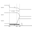
- FIG. 2 is a diagram showing a general method of setting dead time DT.
- the gate-source voltage Vgs (Q1) of the transistor Q1, the drain-source current Ids (Q1) of the transistor Q1, the drain-source voltage Vds (Q1) of the transistor Q1, and The gate-source voltage Vgs(Q2) of transistor Q2 is depicted.
- the measurement of the dead time DT is started at the timing when the dead time DT starts to decrease.
- the gate-source voltage Vgs (Q1) of the transistor Q1 has not fallen below the plateau voltage Vp. Therefore, transistor Q1 still remains on. That is, the drain-source current Ids(Q1) of the transistor Q1 continues to flow as before time t101. Further, the drain-source voltage Vds (Q1) of the transistor Q1 is maintained at approximately 0V.
- the gate-source voltage Vgs (Q1) of the transistor Q1 has a slow falling speed during the transition from the high level to the low level (near the plateau voltage Vp). Therefore, if the above dead time DT is short, as shown at time t103, the gate-source voltage Vgs(Q2) of the transistor Q2 increases before the drain-source current Ids(Q1) of the transistor Q1 reaches 0A. The plateau voltage Vp is reached. As a result, both transistors Q1 and Q2 are turned on, so that an excessive through current may flow.
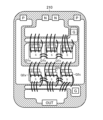
- FIG. 3 is a diagram showing an example of the configuration of the power circuit 200.
- Power circuit 200 of this configuration example includes modules 210 and 220.
- the module 210 includes the aforementioned transistors Q1 and Q2 and forms the first phase of a full-bridge output stage.
- Module 220 includes the aforementioned transistors Q3 and Q4 and forms the second phase of the full-bridge output stage.
- the transistor Q1 includes three unit transistors Q1a, Q1b, and Q1c connected in parallel between the positive end of the DC power supply 2 and the first end of the load 3.
- Body diodes D1a, D1b and D1c are associated with unit transistors Q1a, Q1b and Q1c, respectively.
- the transistor Q2 includes three unit transistors Q2a, Q2b, and Q2c connected in parallel between the first end of the load 3 and the negative end of the DC power supply 2.
- Body diodes D2a, D2b and D2c are associated with unit transistors Q2a, Q2b and Q2c, respectively.
- Transistor Q3 includes three unit transistors Q3a, Q3b, and Q3c connected in parallel between the positive end of DC power supply 2 and the second end of load 3.
- Body diodes D3a, D3b and D3c are associated with unit transistors Q3a, Q3b and Q3c, respectively.
- Transistor Q4 includes three unit transistors Q4a, Q4b, and Q4c connected in parallel between the second end of load 3 and the negative end of DC power supply 2.
- Body diodes D4a, D4b and D4c are associated with unit transistors Q4a, Q4b and Q4c, respectively.
- FIG. 4 is a diagram showing an example of the configuration of the module 210.
- the unit transistors Q1a to Q1c and Q2a to Q2c have connections between their respective source pads and the metal frame, between their respective gate pads and the metal frame, and between their respective source pads. , a large number of wires are bonded.
- the module 220 has the same configuration as the module 210. Therefore, the module 220 can be understood by replacing the unit transistors Q1a to Q1c and Q2a to Q2c in the figure with unit transistors Q3a to Q3c and Q4a to Q4c, respectively.
- FIG. 5 is a diagram showing an equivalent circuit of the module 210 (or 220) as seen from the switch driving device 100.
- the module 210 when viewed from the switch driving device 100, the module 210 includes a gate resistor Rg and N unit transistors (according to FIGS. 3 and 4, three unit transistors Q1a to Q1c or Q2a to Q2c) can be understood as an RC time constant circuit formed by the respective input capacitance Ciss.
- the freewheeling current can only flow through the module 210 for a short time (for example, 500 ns)
- the dead time DT described above is set to a short time (for example, 2 ⁇ s)
- the transistors Q1 and Q2 The risk of simultaneous on-on will increase.
- ⁇ Dead time setting method (new)> 6 and 7 are diagrams each showing a new method of setting the dead time DT.
- the gate-source voltage Vgs (Q1) of the transistor Q1 the gate-source voltage Vgs (Q1) of the transistor Q1, the drain-source current Ids (Q1) of the transistor Q1, and the drain-source voltage Vds (Q1) of the transistor Q1 are shown. Each is depicted.
- FIG. 6 shows behavior under heavy load, for example.
- the gate-source voltage Vgs (Q1) of transistor Q1 begins to decrease from high level to low level. However, at this point, the gate-source voltage Vgs (Q1) of the transistor Q1 has not fallen below the plateau voltage Vp. Therefore, transistor Q1 still remains on. In other words, the drain-source current Ids(Q1) of the transistor Q1 continues to flow as before time t201. Further, the drain-source voltage Vds (Q1) of the transistor Q1 is maintained at approximately 0V.
- time measurement of delay time Td (for example, 500 ns) is started.
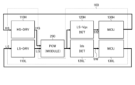
- FIG. 8 is a diagram showing a first embodiment (outline) of the switch driving device 100. In particular, this figure depicts functional blocks of the switch driving device 100 in the first embodiment.
- the switch driving device 100 of this embodiment includes an upper driver 110H, a lower driver 110L, detection circuits 120L and 120H, and control circuits 130L and 130H.
- the upper driver 110H receives the upper control signal HS from the control circuit 130H and amplifies it to generate the upper drive signal HG. Then, the upper driver 110H outputs the upper drive signal HG to the power circuit 200 to turn on/off the transistor Q1 (or the transistor Q3, hereinafter the same) of the power circuit 200.
- the lower driver 110L receives the lower control signal LS from the control circuit 130L and amplifies it to generate the lower drive signal LG. Then, the lower driver 110L outputs the lower drive signal LG to the power circuit 200 to turn on/off the transistor Q2 (or the transistor Q4, hereinafter the same) of the power circuit 200.
- the detection circuit 120L detects that the switch voltage Vsw appearing at the connection node between the transistor Q1 and the transistor Q2 falls, and generates the detection signal S16.
- the fall of the switch voltage Vsw can be understood as a fall of the drain-source voltage Vds (Q2) of the transistor Q2 or a rise of the drain-source voltage Vds (Q1) of the transistor Q1.
- fall of the lower drive signal LG can be understood as the fall of the gate-source voltage Vgs (Q2) of the transistor Q2.
- FIG. 9 is a diagram showing a first embodiment (simplified) of the switch driving device 100. In particular, this figure simply depicts the internal configuration of some of the functional blocks in FIG. 8 mentioned earlier.
- the upper driver 110H receives the upper control signal HS from the control circuit 130H and outputs the upper drive signal HG to the gate of the transistor Q1.
- the transistor Q1 is turned on when the upper drive signal HG is at a high level, and is turned off when the upper drive signal HG is at a low level.
- the lower driver 110L receives the lower control signal LS from the control circuit 130L and outputs the lower drive signal LG to the gate of the transistor Q2.
- the transistor Q2 is turned on when the lower drive signal LG is at a high level, and turned off when the lower drive signal LG is at a low level.
- the detection circuit 120L monitors the switch voltage Vsw to detect the fall of the drain-source voltage Vds (Q2) of the transistor Q2 (and the rise of the drain-source voltage Vds (Q1) of the transistor Q1). A detection signal S16 is generated.
- the detection circuit 120H generates the detection signal S12 by monitoring the lower drive signal LG and detecting the fall of the gate-source voltage Vgs (Q2) of the transistor Q2.
- the control circuit 130L receives the detection signal S16 from the detection circuit 120L and outputs the lower control signal LS to the lower driver 110L.
- the control circuit 130L includes a control section 131L, a delay section 132L, and an AND gate 133L.
- the AND gate 133L (corresponding to the first calculation section) performs an AND operation on the control signal S15 and the delay signal S17 to generate an AND signal S18.
- the AND signal S18 becomes a high level when both the control signal S15 and the delay signal S17 are at a high level, and becomes a low level when at least one of the control signal S15 and the delay signal S17 is at a low level.
- the AND signal S18 is output to the lower driver 110L as the lower control signal LS.
- the control circuit 130H receives the detection signal S12 from the detection circuit 120H and outputs the upper control signal HS to the upper driver 110H.
- the control circuit 130H includes a control section 131H, a delay section 132H, and an AND gate 133H.
- the delay time Td2 may be the same value as the delay time Td1 (for example, 500 ns).
- the AND gate 133H (corresponding to a second calculation unit) performs a logical product operation on the control signal S11 and the delayed signal S13 to generate a logical product signal S14.
- the AND signal S14 becomes high level when both the control signal S11 and the delayed signal S13 are high level, and becomes low level when at least one of the control signal S11 and the delayed signal S13 is low level.
- the AND signal S14 is output to the upper driver 110H as the upper control signal HS.
- FIG. 10 is a diagram showing the first embodiment (details) of the switch driving device 100.
- this figure depicts in detail the internal configuration of the functional blocks in FIGS. 8 and 9 previously mentioned.
- the detection circuit 120H includes a comparator CMP1.
- Comparator CMP1 generates a detection signal S12 by comparing the lower drive signal LG input to the inverting input terminal (-) and a predetermined threshold voltage V11 input to the non-inverting input terminal (+). . Therefore, the detection signal S12 becomes a low level when the lower drive signal LG is higher than the threshold voltage V11, and becomes a high level when the lower drive signal LG is lower than the threshold voltage V11.
- the threshold voltage V11 is set to an appropriate value so that the comparator CMP1 is unlikely to malfunction. For example, when the lower drive signal LG is pulse-driven between 5V and 0V, the threshold voltage V11 may be set to 2V.
- the detection circuit 120L includes resistors R1 and R2 and a comparator CMP2.
- the first end of the resistor R1 is connected to the application end of the switch voltage Vsw.
- the second end of the resistor R1 and the first end of the resistor R2 are both connected to the application end of the divided voltage V12.
- a second end of the resistor R2 is connected to a ground terminal.
- the comparator CMP2 generates the detection signal S16 by comparing the divided voltage V12 input to the inverting input terminal (-) and the threshold voltage V13 input to the non-inverting input terminal (+). Therefore, the detection signal S16 becomes a low level when the divided voltage V12 is higher than the threshold voltage V13, and becomes a high level when the divided voltage V12 is lower than the threshold voltage V13.
- the logic level of the detection signal S16 is switched at the timing when the switch voltage Vsw falls below VDD/2 (for example, 200 to 400 V) with respect to the power supply voltage VDD (for example, 400 to 800 V) applied to the positive terminal of the DC power supply 2.
- VDD/2 for example, 200 to 400 V
- VDD for example, 400 to 800 V
- the voltage division ratio of the divided voltage V12 and the threshold voltage V13 may be set.
- the threshold voltage V13 is set to an appropriate value so that the comparator CMP2 is unlikely to malfunction. For example, when the power supply voltage VDD is 400V and the voltage division ratio of the divided voltage V12 is 1/400, the threshold voltage V13 may be set to 0.5V.
- the control circuit 130 is a functional block that includes the previously mentioned control circuits 130L and 130H. Referring to the figure, the control circuit 130 includes a control section 131, delay sections 132L and 132H, AND gates 133L and 133H, and NOR gates 134 and 135.
- the control circuit 130 may be, for example, an MCU (micro controller unit).
- the control unit 131 is a functional unit that includes the previously mentioned control units 131L and 131H. Referring to the figure, the control section 131 includes a delay section 131a, an AND gate 131b, and a NOR gate 131c.
- the delay unit 131a delays the reference control signal S1 to generate a delayed control signal S2.
- the AND gate 131b performs an AND operation on the reference control signal S1 and the delayed control signal S2 to generate the previously mentioned control signal S11. Therefore, the control signal S11 is at a high level when both the reference control signal S1 and the delayed control signal S2 are at a high level, and is at a low level when at least one of the reference control signal S1 and the delayed control signal S2 is at a low level. becomes.
- the NOR gate 131c performs a NOR operation on the reference control signal S1 and the delayed control signal S2 to generate the previously mentioned control signal S15. Therefore, the control signal S15 is at a high level when both the reference control signal S1 and the delayed control signal S2 are at a low level, and is at a low level when at least one of the reference control signal S1 and the delayed control signal S2 is at a high level. becomes.
- the delay unit 132L delays the detection signal S16 by a delay time Td1 (for example, 500 ns) to generate a delayed signal S17.
- Td1 for example, 500 ns
- the delay unit 132H generates a delayed signal S13 by delaying the detection signal S12 (latch detection signal S19 in this figure) by a delay time Td2 (for example, 500 ns).
- the first input terminal of the NOR gate 134 is connected to the application terminal of the detection signal S12.
- the second input terminal of the NOR gate 134 and the output terminal of the NOR gate 135 are both connected to the application terminal of the latch detection signal S19.
- a first input terminal of NOR gate 135 is connected to an output terminal of NOR gate 134.
- a second input terminal of the NOR gate 135 is connected to an application terminal of the control signal S15.
- the NOR gates 134 and 135 connected in this way function as an RS flip-flop that generates the latch detection signal S19 according to the detection signal S12 and the control signal S15.
- the latch detection signal S19 is set to a high level at a pulse edge of the detection signal S12, and reset to a low level at a pulse edge of the control signal S15. Therefore, protection is applied so that the high levels of the detection signal S12 and the control signal S15 do not overlap.
- the upper driver 110H receives the upper control signal HS and outputs the upper drive signal HG.
- a gate resistor RgH may be connected between the output end of the upper driver 110H and the gate of the transistor Q1.
- the lower driver 110L receives the lower control signal LS and outputs the lower drive signal LG.
- a gate resistor RgL may be connected between the output end of the lower driver 110L and the gate of the transistor Q2.
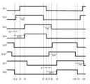
- FIG. 11 is a diagram showing the dead time setting operation in the first embodiment.
- the control signal S11, the detection signal S12, the delayed signal S13, the AND signal S14, the control signal S15, the detection signal S16, the delayed signal S17, and the AND signal S18 are depicted in order from the top.
- the lower drive signal LG falls below the plateau voltage Vp and further below the threshold voltage V11.
- the detection signal S12 rises to high level.
- the delay signal S13 is maintained at a low level until a delay time Td2 (for example, 500 ns) elapses after the detection signal S12 rises to a high level.
- the detection signal S12 falls to a low level at time t5
- the delayed signal S13 falls to a low level at a time t8 after a delay time Td2.
- the AND signal S14 also falls to a low level without delay.
- the detection signal S16 rises to high level.
- the delay signal S17 is maintained at a low level until a delay time Td1 (for example, 500 ns) has elapsed after the detection signal S16 rises to a high level.
- the detection signal S16 falls to a low level at time t10
- the delayed signal S17 falls to a low level at time t12 after a delay time Td1.
- the control signal S15 falls to a low level
- the AND signal S18 also falls to a low level without delay.
- transistors Q1 and Q2 simultaneously Hard to turn on. Therefore, generation of excessive through current is prevented.
- FIG. 12 is a diagram showing a second embodiment (outline) of the switch driving device 100.
- the switch driving device 100 of this embodiment is based on the first embodiment (FIG. 8) described above, but includes a detection circuit 120L' in place of the detection circuit 120L.
- the detection circuit 120L' detects that the transistor Q1 actually transitions to the off state after the upper control signal HS is switched to low level, and generates the detection signal S16'.
- the detection circuit 120L' detects that the switch current flowing through the transistor Q1, that is, the drain-source current Ids (Q1) of the transistor Q1 falls, and generates the detection signal S16'.
- FIG. 13 is a diagram showing a second embodiment (simplified) of the switch driving device 100.
- the detection circuit 120L' is connected between the sources of the transistors Q2 and Q4 and the ground terminal, and detects the fall of the drain-source current Ids (Q4) of the transistor Q4. , and in turn, detects the fall of the drain-source current Ids (Q1) of the transistor Q1 to generate a detection signal S16'.
- FIG. 14 is a diagram showing the second embodiment (details) of the switch driving device 100.
- this figure depicts in detail the internal configuration of the functional blocks in FIGS. 12 and 13 mentioned above.
- a capacitor 4 may be connected between the positive and negative ends of the DC power supply 2.
- the detection circuit 120L' includes a resistor R3, an amplifier AMP1, and a comparator CMP3.
- the first end of the resistor R3 is connected to the source of the transistor Q2.
- the non-inverting input terminal (+) of the amplifier AMP1 is connected to the first terminal of the resistor R3.
- the inverting input terminal (-) of the amplifier AMP1 is connected to the second terminal of the resistor R3.
- the amplifier AMP1 connected in this way amplifies the detection voltage V21 appearing across the resistor R3 to generate an amplified voltage V22.
- the comparator CMP3 compares the amplified voltage V22 input to the inverting input terminal (-) and the threshold voltage V23 input to the non-inverting input terminal (+) to generate a detection signal S16'. Therefore, the detection signal S16' becomes low level when the amplified voltage V22 is higher than the threshold voltage V23, and becomes high level when the amplified voltage V22 is lower than the threshold voltage V23.
- FIG. 15 is a diagram showing the dead time setting operation in the second embodiment.
- the control signal S11, the detection signal S12, the delayed signal S13, the AND signal S14, the control signal S15, the detection signal S16', the delayed signal S17, and the AND signal S18 are depicted in order from the top. .
- the content of this figure is the same as that of the first embodiment (FIG. 11) described earlier, except that the detection signal S16 is replaced with the detection signal S16'. Focusing on the difference from the first embodiment (FIG. 11), at time t7, when the off time ⁇ 1 of the transistor Q1 has elapsed, the upper drive signal HG (not shown) falls below the plateau voltage Vp. Therefore, the drain-source current Ids (Q1) of the transistor Q1 falls, and the detection voltage V22 falls below the threshold voltage V23. As a result, the detection signal S16' rises to high level.
- transistors Q1 and Q2 simultaneously Hard to turn on. Therefore, generation of excessive through current is prevented.
- FIG. 16 is a diagram showing a third embodiment (outline) of the switch driving device 100.
- the switch driving device 100 of this embodiment is based on the first embodiment (FIG. 8) described above, but includes a detection circuit 120L'' in place of the detection circuit 120L.
- the detection circuit 120L'' detects that the transistor Q1 actually transitions to the off state after the upper control signal HS is switched to low level, and generates the detection signal S16''.
- the fall of the upper drive signal HG can be understood as the fall of the gate-source voltage Vgs (Q1) of the transistor Q1.
- FIG. 17 is a diagram showing a third embodiment (simplified) of the switch driving device 100.
- the detection circuit 120L'' generates the detection signal S16'' by monitoring the upper drive signal HG and detecting the fall of the gate-source voltage Vgs (Q1) of the transistor Q1. do.
- FIG. 18 is a diagram showing the third embodiment (details) of the switch driving device 100. In particular, this figure depicts in detail the internal configuration of the functional blocks in FIGS. 16 and 17.
- the detection circuit 120L'' includes an amplifier AMP2 and a comparator CMP4.
- the comparator CMP4 compares the amplified voltage V31 input to the inverting input terminal (-) and the threshold voltage V32 input to the non-inverting input terminal (+) to generate a detection signal S16''. Therefore, the detection signal S16'' becomes a low level when the amplified voltage V31 is higher than the threshold voltage V32, and becomes a high level when the amplified voltage V31 is lower than the threshold voltage V32.
- Control circuit 130 includes NOR gates 136 and 137 in addition to the aforementioned components 131-135.
- the first input terminal of the NOR gate 136 is connected to the application terminal of the detection signal S16''.
- the second input terminal of the NOR gate 136 and the output terminal of the NOR gate 137 are both connected to the application terminal of the latch detection signal S20.
- a first input terminal of the NOR gate 137 is connected to an output terminal of the NOR gate 136.
- a second input terminal of the NOR gate 137 is connected to an application terminal of the control signal S11.
- the NOR gates 136 and 137 connected in this manner function as an RS flip-flop that generates the latch detection signal S20 in response to the detection signal S16'' and the control signal S11.
- the latch detection signal S20 is " is set to high level at the pulse edge of control signal S11, and reset to low level at the pulse edge of control signal S11. Therefore, protection is applied so that the high levels of the detection signal S16'' and the control signal S11 do not overlap.
- FIG. 19 is a diagram showing the dead time setting operation in the third embodiment.
- the control signal S11, detection signal S12, delay signal S13, AND signal S14, control signal S15, detection signal S16'', delay signal S17, and AND signal S18 are depicted in order from the top. .
- transistors Q1 and Q2 simultaneously Hard to turn on. Therefore, generation of excessive through current is prevented.
- the switch driving device disclosed herein includes an upper driver configured to receive an input of an upper control signal and output an upper drive signal to turn on/off an upper switch of a power circuit.
- a lower driver configured to receive a lower control signal and output a lower drive signal to turn on/off a lower switch of the power circuit; and the upper control signal is at an off logic level.
- the switch voltage appearing at the connection node between the upper switch and the lower switch has fallen, the switch current flowing through the upper switch has fallen, or the upper drive signal has reached an off logic level.
- a first detection circuit configured to generate a first detection signal by detecting that the first detection signal has been switched to the lower side control signal;
- a first control circuit configured to switch to an on logic level (first configuration).
- the first detection circuit has a configuration (a second detection circuit) that generates the first detection signal by comparing the switch voltage or its divided voltage with a predetermined threshold voltage. configuration).
- the first detection circuit generates the first detection signal by comparing a detection voltage corresponding to the switch current or an amplified voltage thereof with a predetermined threshold voltage.
- configuration (third configuration).
- the first detection circuit compares a differential voltage between the upper drive signal and the switch voltage or an amplified voltage thereof with a predetermined threshold voltage to detect the first detection circuit.
- a configuration (fourth configuration) that generates a signal may also be used.
- the first control circuit includes a first control section configured to generate a first control signal, and a first control section configured to generate a first control signal; a first delay unit configured to generate a first delayed signal by delaying by a first delay time; and a first delay unit configured to perform a logical operation on the first control signal and the first delayed signal to generate the lower control signal.
- the switch driving device detecting that the lower drive signal is switched to the off logic level after the lower control signal is switched to the off logic level; a second detection circuit configured to generate a second detection signal; and configured to switch the upper control signal to an on logic level after at least a second delay time has elapsed using the second detection signal as a trigger.
- the configuration may further include a second control circuit (sixth configuration).
- the second detection circuit has a configuration (seventh configuration) that generates the second detection signal by comparing the lower drive signal with a predetermined threshold voltage. It's okay.
- the second control circuit includes a second control section configured to generate a second control signal, and a second control section configured to generate a second control signal, and a second control section configured to generate a second control signal; a second delay unit configured to generate a second delayed signal by delaying by a time; and configured to perform a logical operation on the second control signal and the second delayed signal to generate the upper control signal.
- a configuration (eighth configuration) including a second calculation section may also be adopted.
- the inverter circuit disclosed in this specification has a configuration (ninth configuration) including the switch driving device according to any of the first to eighth configurations described above and the power circuit.
- the power circuit may be configured as a module including the upper switch and the lower switch (a tenth configuration).
- the upper switch and the lower switch may each include a plurality of unit transistors connected in parallel (an eleventh configuration).
- the upper switch and the lower switch may each be a SiC device (twelfth configuration).
Abstract
A switch drive device 100 comprises: an upper driver 110H that switches an upper switch of a power circuit 200 on/off by receiving input of an upper control signal HS and outputting a upper drive signal HG; a lower driver 110L that switches a lower switch of the power circuit 200 on/off by receiving input of a lower control signal LS and outputting a lower drive signal LG; a first detection circuit 120L that detects falling of a switch voltage which appears at a connection node between the upper switch and the lower switch after the upper control signal HS has been switched to an off logic level (for example, a low level) and that generates a first detection signal S16; and a first control circuit 130L that switches the lower control signal LS to an on logic level (for example, a high level) after at least a first delay time has elapsed, using the first detection signal S16 as a trigger.
Description
本開示は、スイッチ駆動装置及びこれを用いたインバータ回路に関する。
The present disclosure relates to a switch drive device and an inverter circuit using the same.
ハーフブリッジ出力段又はフルブリッジ出力段の上側スイッチ及び下側スイッチを相補的にオン/オフするスイッチ駆動装置では、貫通電流防止のために上側スイッチ及び下側スイッチの双方をオフ状態とするデッドタイム(=同時オン防止期間)が設けられる。
In a switch drive device that turns on/off the upper switch and lower switch of a half-bridge output stage or full-bridge output stage in a complementary manner, there is a dead time in which both the upper switch and the lower switch are turned off to prevent through current. (=simultaneous ON prevention period) is provided.
なお、上記に関連する従来技術の一例としては、特許文献1を挙げることができる。
Incidentally, Patent Document 1 can be mentioned as an example of the conventional technology related to the above.
しかしながら、従来のスイッチ駆動装置では、デッドタイムの設定手法について検討の余地があった。
However, in the conventional switch drive device, there is room for consideration regarding the dead time setting method.
例えば、本明細書中に開示されているスイッチ駆動装置は、上側制御信号の入力を受けて上側駆動信号を出力することによりパワー回路の上側スイッチをオン/オフするように構成された上側ドライバと、下側制御信号の入力を受けて下側駆動信号を出力することにより前記パワー回路の下側スイッチをオン/オフするように構成された下側ドライバと、前記上側制御信号がオフ論理レベルに切り替えられてから、前記上側スイッチと前記下側スイッチとの接続ノードに現れるスイッチ電圧が立ち下がったこと、前記上側スイッチに流れるスイッチ電流が立ち下がったこと、又は、前記上側駆動信号がオフ論理レベルに切り替わったことを検出して第1検出信号を生成するように構成された第1検出回路と、前記第1検出信号をトリガとして少なくとも第1遅延時間が経過してから前記下側制御信号をオン論理レベルに切り替えるように構成された第1制御回路と、を備える。
For example, the switch driving device disclosed herein includes an upper driver configured to receive an input of an upper control signal and output an upper drive signal to turn on/off an upper switch of a power circuit. a lower driver configured to receive a lower control signal and output a lower drive signal to turn on/off a lower switch of the power circuit; and the upper control signal is at an off logic level. After switching, the switch voltage appearing at the connection node between the upper switch and the lower switch has fallen, the switch current flowing through the upper switch has fallen, or the upper drive signal has reached an off logic level. a first detection circuit configured to generate a first detection signal by detecting that the first detection signal has been switched to the lower side control signal; a first control circuit configured to switch to an on logic level.
なお、その他の特徴、要素、ステップ、利点、及び、特性については、以下に続く発明を実施するための形態及びこれに関する添付の図面によって、さらに明らかとなる。
Note that other features, elements, steps, advantages, and characteristics will become clearer from the detailed description and accompanying drawings that follow.
本開示によれば、デッドタイムを適切に設定することのできるスイッチ駆動装置、及びこれを用いたインバータ回路を提供することが可能となる。
According to the present disclosure, it is possible to provide a switch driving device that can appropriately set dead time, and an inverter circuit using the same.
<インバータ回路>
図1は、インバータ回路の一構成例を示す図である。本構成例のインバータ回路1は、直流電源2から直流電力の入力を受けて負荷3に交流電力を出力する電力変換装置の一種である。本図に即して述べると、インバータ回路1は、スイッチ駆動装置100とパワー回路200を備える。 <Inverter circuit>
FIG. 1 is a diagram showing an example of the configuration of an inverter circuit. Theinverter circuit 1 of this configuration example is a type of power converter that receives input of DC power from a DC power supply 2 and outputs AC power to a load 3. Referring to the figure, the inverter circuit 1 includes a switch drive device 100 and a power circuit 200.
図1は、インバータ回路の一構成例を示す図である。本構成例のインバータ回路1は、直流電源2から直流電力の入力を受けて負荷3に交流電力を出力する電力変換装置の一種である。本図に即して述べると、インバータ回路1は、スイッチ駆動装置100とパワー回路200を備える。 <Inverter circuit>
FIG. 1 is a diagram showing an example of the configuration of an inverter circuit. The
スイッチ駆動装置100は、パワー回路200を駆動するための半導体装置(いわゆるゲートドライバIC[integrated circuit])である。
The switch driving device 100 is a semiconductor device (so-called gate driver IC [integrated circuit]) for driving the power circuit 200.
パワー回路200は、スイッチ駆動装置100からゲート駆動信号の入力を受けて負荷3に交流電力を出力する。本図に即して述べると、パワー回路200は、トランジスタQ1~Q4を含む。トランジスタQ1~Q4は、例えば、SiCデバイスであってもよい。
The power circuit 200 receives a gate drive signal from the switch drive device 100 and outputs AC power to the load 3. Referring to the figure, power circuit 200 includes transistors Q1 to Q4. Transistors Q1-Q4 may be SiC devices, for example.
トランジスタQ1のドレインは、直流電源2の正極端に接続されている。トランジスタQ1のソースは、負荷3の第1端に接続されている。トランジスタQ1のゲートは、スイッチ駆動装置100に接続されている。このように接続されたトランジスタQ1は、フルブリッジ出力段を形成する第1相の上側スイッチとして機能する。
The drain of the transistor Q1 is connected to the positive terminal of the DC power supply 2. The source of transistor Q1 is connected to the first end of load 3. The gate of transistor Q1 is connected to switch driving device 100. Transistor Q1 connected in this way functions as the upper switch of the first phase forming a full-bridge output stage.
トランジスタQ2のドレインは、負荷3の第1端に接続されている。トランジスタQ2のソースは、直流電源2の負極端(接地端)に接続されている。トランジスタQ2のゲートは、スイッチ駆動装置100に接続されている。このように接続されたトランジスタQ2は、フルブリッジ出力段を形成する第1相の下側スイッチとして機能する。
The drain of the transistor Q2 is connected to the first end of the load 3. The source of transistor Q2 is connected to the negative terminal (ground terminal) of DC power supply 2. The gate of transistor Q2 is connected to switch driving device 100. Transistor Q2 connected in this way functions as the lower switch of the first phase forming a full-bridge output stage.
トランジスタQ3のドレインは、直流電源2の正極端に接続されている。トランジスタQ3のソースは、負荷3の第2端に接続されている。トランジスタQ3のゲートは、スイッチ駆動装置100に接続されている。このように接続されたトランジスタQ3は、フルブリッジ出力段を形成する第2相の上側スイッチとして機能する。
The drain of the transistor Q3 is connected to the positive terminal of the DC power supply 2. The source of transistor Q3 is connected to the second end of load 3. The gate of transistor Q3 is connected to switch driver 100. Transistor Q3 connected in this way functions as the upper switch of the second phase forming a full-bridge output stage.
トランジスタQ4のドレインは、負荷3の第2端に接続されている。トランジスタQ4のソースは、直流電源2の負極端(接地端)に接続されている。トランジスタQ4のゲートは、スイッチ駆動装置100に接続されている。このように接続されたトランジスタQ4は、フルブリッジ出力段を形成する第2相の下側スイッチとして機能する。
The drain of the transistor Q4 is connected to the second end of the load 3. The source of transistor Q4 is connected to the negative terminal (ground terminal) of DC power supply 2. The gate of transistor Q4 is connected to switch driving device 100. Transistor Q4 connected in this way functions as the lower switch of the second phase forming a full-bridge output stage.
なお、トランジスタQ1~Q4には、それぞれ、トランジスタQ1~Q4それぞれのドレインをカソードとして、トランジスタQ1~Q4それぞれのソースをアノードとするボディダイオードD1~D4が付随する。
Note that body diodes D1 to D4 are attached to the transistors Q1 to Q4, respectively, with the drains of the transistors Q1 to Q4 serving as cathodes, and the sources of the transistors Q1 to Q4 serving as anodes.
ところで、インバータ回路1に接続される負荷3が誘導性負荷(モータコイルなど)である場合には、トランジスタQ1~Q4がいずれもオフ状態とされた直後において、負荷3の誘導起電力により通常電流とは逆向きの還流電流が流れ得る。
By the way, when the load 3 connected to the inverter circuit 1 is an inductive load (such as a motor coil), the normal current increases due to the induced electromotive force of the load 3 immediately after all of the transistors Q1 to Q4 are turned off. A return current may flow in the opposite direction.
例えば、トランジスタQ1及びQ4がいずれもオン状態であり、トランジスタQ2及びQ3がいずれもオフ状態である場合を考える。この場合、パワー回路200には、直流電源2の正極端からトランジスタQ1、負荷3及びトランジスタQ4を介して直流電源2の負極端に至る電流経路L1に通常電流が流れる。
For example, consider a case where transistors Q1 and Q4 are both in an on state, and transistors Q2 and Q3 are both in an off state. In this case, in the power circuit 200, a normal current flows through a current path L1 from the positive end of the DC power supply 2 to the negative end of the DC power supply 2 via the transistor Q1, the load 3, and the transistor Q4.
次に、上記の通常電流が流れている状態からトランジスタQ1及びQ3がいずれもオフ状態に切り替えられた場合を考える。この場合、パワー回路200には、直流電源2の負極端からボディダイオードD2、負荷3及びボディダイオードD3を介して直流電源2の正極端に至る電流経路L2に還流電流が流れる。
Next, consider a case where both transistors Q1 and Q3 are switched to the off state from the state where the above-mentioned normal current is flowing. In this case, in the power circuit 200, a return current flows through a current path L2 from the negative end of the DC power supply 2 to the positive end of the DC power supply 2 via the body diode D2, the load 3, and the body diode D3.
また、改めて図示はしないが、トランジスタQ2及びQ3のオフ遷移時には、直流電源2の負極端からボディダイオードD4、負荷3及びボディダイオードD1を介して直流電源2の正極端に至る電流経路にも還流電流が流れ得る。
Although not shown in the drawing, when the transistors Q2 and Q3 turn off, a current flows back through the current path from the negative end of the DC power supply 2 to the positive end of the DC power supply 2 via the body diode D4, the load 3, and the body diode D1. Current can flow.
そのため、スイッチ駆動装置100では、上側スイッチ及び下側スイッチの双方をオフ状態とするデッドタイムDT(=同時オン防止期間)が適切に設定されていることが重要となる。
Therefore, in the switch driving device 100, it is important that the dead time DT (=simultaneous on prevention period) for turning off both the upper switch and the lower switch is appropriately set.
<デッドタイム設定手法(一般)>
図2は、デッドタイムDTの一般的な設定手法を示す図である。本図では、上から順番に、トランジスタQ1のゲート・ソース間電圧Vgs(Q1)、トランジスタQ1のドレイン・ソース間電流Ids(Q1)、トランジスタQ1のドレイン・ソース間電圧Vds(Q1)、及び、トランジスタQ2のゲート・ソース間電圧Vgs(Q2)がそれぞれ描写されている。 <Dead time setting method (general)>
FIG. 2 is a diagram showing a general method of setting dead time DT. In this figure, in order from the top, the gate-source voltage Vgs (Q1) of the transistor Q1, the drain-source current Ids (Q1) of the transistor Q1, the drain-source voltage Vds (Q1) of the transistor Q1, and The gate-source voltage Vgs(Q2) of transistor Q2 is depicted.
一般的なデッドタイム設定手法では、時刻t101において、トランジスタQ1のゲート・ソース間電圧Vgs(Q1)がハイレベル(=トランジスタQ1のオン論理レベル)からローレベル(=トランジスタQ1のオフ論理レベル)に向けて低下し始めるタイミングで、デッドタイムDTの計時が開始されている。
In the general dead time setting method, at time t101, the gate-source voltage Vgs (Q1) of transistor Q1 changes from high level (=on logic level of transistor Q1) to low level (=off logic level of transistor Q1). The measurement of the dead time DT is started at the timing when the dead time DT starts to decrease.
なお、この時点では、トランジスタQ1のゲート・ソース間電圧Vgs(Q1)がプラトー電圧Vpを下回っていない。従って、トランジスタQ1は、未だオン状態のままである。すなわち、トランジスタQ1のドレイン・ソース間電流Ids(Q1)は、時刻t101以前と同様に流れ続けている。また、トランジスタQ1のドレイン・ソース間電圧Vds(Q1)は、ほぼ0Vに維持されている。
Note that at this point, the gate-source voltage Vgs (Q1) of the transistor Q1 has not fallen below the plateau voltage Vp. Therefore, transistor Q1 still remains on. That is, the drain-source current Ids(Q1) of the transistor Q1 continues to flow as before time t101. Further, the drain-source voltage Vds (Q1) of the transistor Q1 is maintained at approximately 0V.
時刻t102において、デッドタイムDTの計時が完了されると、トランジスタQ2のゲート・ソース間電圧Vgs(Q2)がローレベル(=トランジスタQ2のオフ論理レベル)からハイレベル(=トランジスタQ1のオン論理レベル)に向けて上昇し始める。
At time t102, when the measurement of dead time DT is completed, the gate-source voltage Vgs (Q2) of transistor Q2 changes from a low level (=off logic level of transistor Q2) to a high level (=on logic level of transistor Q1). ) begins to rise towards.
ところで、トランジスタQ1のゲート・ソース間電圧Vgs(Q1)は、ハイレベルからローレベルへの遷移途中(=プラトー電圧Vpの近傍)で立ち下がり速度が遅くなる。そのため、上記のデッドタイムDTが短いと、時刻t103で示したように、トランジスタQ1のドレイン・ソース間電流Ids(Q1)が0Aになる前にトランジスタQ2のゲート・ソース間電圧Vgs(Q2)がプラトー電圧Vpに達してしまう。その結果、トランジスタQ1及びQ2がいずれもオン状態となるので、過大な貫通電流が流れ得る。
By the way, the gate-source voltage Vgs (Q1) of the transistor Q1 has a slow falling speed during the transition from the high level to the low level (near the plateau voltage Vp). Therefore, if the above dead time DT is short, as shown at time t103, the gate-source voltage Vgs(Q2) of the transistor Q2 increases before the drain-source current Ids(Q1) of the transistor Q1 reaches 0A. The plateau voltage Vp is reached. As a result, both transistors Q1 and Q2 are turned on, so that an excessive through current may flow.
なお、改めて図示はしないが、トランジスタQ3及びQ4についても上記と同様の挙動で貫通電流が流れ得る。
Note that although not shown in the drawings, a through current may flow in the transistors Q3 and Q4 with the same behavior as described above.
図3はパワー回路200の一構成例を示す図である。本構成例のパワー回路200は、モジュール210及び220を含む。
FIG. 3 is a diagram showing an example of the configuration of the power circuit 200. Power circuit 200 of this configuration example includes modules 210 and 220.
モジュール210は、先出のトランジスタQ1及びQ2を含み、フルブリッジ出力段の第1相を形成する。モジュール220は、先出のトランジスタQ3及びQ4を含み、フルブリッジ出力段の第2相を形成する。
The module 210 includes the aforementioned transistors Q1 and Q2 and forms the first phase of a full-bridge output stage. Module 220 includes the aforementioned transistors Q3 and Q4 and forms the second phase of the full-bridge output stage.
トランジスタQ1は、直流電源2の正極端と負荷3の第1端との間に並列接続された3つの単位トランジスタQ1a、Q1b及びQ1cを含む。単位トランジスタQ1a、Q1b及びQ1cには、それぞれ、ボディダイオードD1a、D1b及びD1cが付随する。
The transistor Q1 includes three unit transistors Q1a, Q1b, and Q1c connected in parallel between the positive end of the DC power supply 2 and the first end of the load 3. Body diodes D1a, D1b and D1c are associated with unit transistors Q1a, Q1b and Q1c, respectively.
トランジスタQ2は、負荷3の第1端と直流電源2の負極端との間に並列接続された3つの単位トランジスタQ2a、Q2b及びQ2cを含む。単位トランジスタQ2a、Q2b及びQ2cには、それぞれ、ボディダイオードD2a、D2b及びD2cが付随する。
The transistor Q2 includes three unit transistors Q2a, Q2b, and Q2c connected in parallel between the first end of the load 3 and the negative end of the DC power supply 2. Body diodes D2a, D2b and D2c are associated with unit transistors Q2a, Q2b and Q2c, respectively.
トランジスタQ3は、直流電源2の正極端と負荷3の第2端との間に並列接続された3つの単位トランジスタQ3a、Q3b及びQ3cを含む。単位トランジスタQ3a、Q3b及びQ3cには、それぞれ、ボディダイオードD3a、D3b及びD3cが付随する。
Transistor Q3 includes three unit transistors Q3a, Q3b, and Q3c connected in parallel between the positive end of DC power supply 2 and the second end of load 3. Body diodes D3a, D3b and D3c are associated with unit transistors Q3a, Q3b and Q3c, respectively.
トランジスタQ4は、負荷3の第2端と直流電源2の負極端との間に並列接続された3つの単位トランジスタQ4a、Q4b及びQ4cを含む。単位トランジスタQ4a、Q4b及びQ4cには、それぞれ、ボディダイオードD4a、D4b及びD4cが付随する。
Transistor Q4 includes three unit transistors Q4a, Q4b, and Q4c connected in parallel between the second end of load 3 and the negative end of DC power supply 2. Body diodes D4a, D4b and D4c are associated with unit transistors Q4a, Q4b and Q4c, respectively.
図4は、モジュール210の一構成例を示す図である。本図で示すように、単位トランジスタQ1a~Q1c及びQ2a~Q2cには、それぞれのソースパッドとメタルフレームとの間、それぞれのゲートパッドとメタルフレームとの間、及び、それぞれのソースパッド相互間に、多数のワイヤがボンディングされる。
FIG. 4 is a diagram showing an example of the configuration of the module 210. As shown in this figure, the unit transistors Q1a to Q1c and Q2a to Q2c have connections between their respective source pads and the metal frame, between their respective gate pads and the metal frame, and between their respective source pads. , a large number of wires are bonded.
また、改めて図示はしないが、モジュール220は、モジュール210と同様の構成である。従って、本図の単位トランジスタQ1a~Q1c及びQ2a~Q2cをそれぞれ単位トランジスタQ3a~Q3c及びQ4a~Q4cに読み替えれば、モジュール220の説明として理解することができる。
Although not illustrated again, the module 220 has the same configuration as the module 210. Therefore, the module 220 can be understood by replacing the unit transistors Q1a to Q1c and Q2a to Q2c in the figure with unit transistors Q3a to Q3c and Q4a to Q4c, respectively.
図5は、スイッチ駆動装置100から見たモジュール210(又は220)の等価回路を示す図である。本図で示すように、スイッチ駆動装置100から見ると、モジュール210は、ゲート抵抗Rgと、N個の単位トランジスタ(図3及び図4に倣えば、3個の単位トランジスタQ1a~Q1c又はQ2a~Q2c)それぞれの入力容量Cissにより形成されるRC時定数回路として理解され得る。
FIG. 5 is a diagram showing an equivalent circuit of the module 210 (or 220) as seen from the switch driving device 100. As shown in this figure, when viewed from the switch driving device 100, the module 210 includes a gate resistor Rg and N unit transistors (according to FIGS. 3 and 4, three unit transistors Q1a to Q1c or Q2a to Q2c) can be understood as an RC time constant circuit formed by the respective input capacitance Ciss.
すなわち、スイッチ駆動装置100から見たモジュール210の入力容量(=合成容量値)は、Ciss×Nとなる。そのため、トランジスタQ1及びQ2をそれぞれ形成する単位トランジスタの並列数Nが多いほど、入力容量Ciss×Nの放電時間が長くなり、延いては、ゲート・ソース間電圧Vgsの立ち下がりが遅くなる。
That is, the input capacitance (=combined capacitance value) of the module 210 seen from the switch driving device 100 is Ciss×N. Therefore, the greater the number N of unit transistors in parallel forming each of the transistors Q1 and Q2, the longer the discharge time of the input capacitance Ciss×N becomes, and as a result, the fall of the gate-source voltage Vgs becomes slower.
従って、モジュール210には短時間(例えば500ns)しか還流電流を流すことができないという制約の下、先述のデッドタイムDTが短時間(例えば2μs)に設定されている場合には、トランジスタQ1及びQ2の同時オンリスクが増大してしまう。
Therefore, under the constraint that the freewheeling current can only flow through the module 210 for a short time (for example, 500 ns), if the dead time DT described above is set to a short time (for example, 2 μs), the transistors Q1 and Q2 The risk of simultaneous on-on will increase.
<デッドタイム設定手法(新規)>
図6及び図7は、それぞれ、デッドタイムDTの新規な設定手法を示す図である。各図では、上から順番に、トランジスタQ1のゲート・ソース間電圧Vgs(Q1)、トランジスタQ1のドレイン・ソース間電流Ids(Q1)、及び、トランジスタQ1のドレイン・ソース間電圧Vds(Q1)がそれぞれ描写されている。 <Dead time setting method (new)>
6 and 7 are diagrams each showing a new method of setting the dead time DT. In each figure, from the top, the gate-source voltage Vgs (Q1) of the transistor Q1, the drain-source current Ids (Q1) of the transistor Q1, and the drain-source voltage Vds (Q1) of the transistor Q1 are shown. Each is depicted.
なお、図6は、例えば重負荷時の挙動を示している。また、図7は、例えば軽負荷時の挙動を示している。トランジスタQ1のゲート・ソース間電圧Vgs(Q1)がプラトー電圧Vpを下回るまでのオフ時間αに着目すると、図6ではα=Tp1(例えばTp1=1μs)であり、図7ではα=Tp2(例えばTp2=2μs)である。
Note that FIG. 6 shows behavior under heavy load, for example. Further, FIG. 7 shows behavior under light load, for example. Focusing on the off time α until the gate-source voltage Vgs (Q1) of the transistor Q1 falls below the plateau voltage Vp, in FIG. 6, α=Tp1 (for example, Tp1=1 μs), and in FIG. 7, α=Tp2 (for example, Tp2=2μs).
時刻t201では、トランジスタQ1のゲート・ソース間電圧Vgs(Q1)がハイレベルからローレベルに向けて低下し始める。ただし、この時点では、トランジスタQ1のゲート・ソース間電圧Vgs(Q1)がプラトー電圧Vpを下回っていない。従って、トランジスタQ1は、未だオン状態のままである。つまり、トランジスタQ1のドレイン・ソース間電流Ids(Q1)は、時刻t201以前と同様に流れ続けている。また、トランジスタQ1のドレイン・ソース間電圧Vds(Q1)は、ほぼ0Vに維持されている。
At time t201, the gate-source voltage Vgs (Q1) of transistor Q1 begins to decrease from high level to low level. However, at this point, the gate-source voltage Vgs (Q1) of the transistor Q1 has not fallen below the plateau voltage Vp. Therefore, transistor Q1 still remains on. In other words, the drain-source current Ids(Q1) of the transistor Q1 continues to flow as before time t201. Further, the drain-source voltage Vds (Q1) of the transistor Q1 is maintained at approximately 0V.
時刻t202又はt202’において、トランジスタQ1のゲート・ソース間電圧Vgs(Q1)がプラトー電圧Vpを下回るまで低下すると、トランジスタQ1のドレイン・ソース間電流Ids(Q1)が減少し始める。また、トランジスタQ1のドレイン・ソース間電圧Vds(Q1)が上昇し始める。
At time t202 or t202', when the gate-source voltage Vgs(Q1) of the transistor Q1 falls below the plateau voltage Vp, the drain-source current Ids(Q1) of the transistor Q1 begins to decrease. Further, the drain-source voltage Vds (Q1) of the transistor Q1 begins to rise.
そこで、新規なデッドタイム設定手法では、例えば、トランジスタQ1のドレイン・ソース間電圧Vds(Q1)の立ち上がり、または、トランジスタQ1のドレイン・ソース間電流Ids(Q1)の立ち下がりが検出されたときに、遅延時間Td(例えば500ns)の計時が開始される。
Therefore, in the new dead time setting method, for example, when the rise of the drain-source voltage Vds (Q1) of the transistor Q1 or the fall of the drain-source current Ids (Q1) of the transistor Q1 is detected, , time measurement of delay time Td (for example, 500 ns) is started.
その後、時刻t203において、遅延時間Tdの計時が完了されると、図示しないトランジスタQ2のゲート・ソース間電圧Vgs(Q2)がローレベルからハイレベルに向けて上昇し始める。
Thereafter, at time t203, when the measurement of the delay time Td is completed, the gate-source voltage Vgs (Q2) of the transistor Q2 (not shown) begins to rise from the low level to the high level.
上記一連のデッドタイム設定手法であれば、トランジスタQ1のオフ時間αに応じて常に適切なデッドタイムDT(=α+Td)が可変的に確保される。そのため、負荷3に流れる出力電流の変化などにより、トランジスタQ1のオフ時間αが長くなったとしても、トランジスタQ1及びQ2が同時にオン状態となりにくい。従って、過大な貫通電流の発生が防止される。
With the series of dead time setting methods described above, an appropriate dead time DT (=α+Td) is always variably secured according to the off time α of the transistor Q1. Therefore, even if the off time α of the transistor Q1 becomes longer due to a change in the output current flowing through the load 3, it is difficult for the transistors Q1 and Q2 to turn on at the same time. Therefore, generation of excessive through current is prevented.
以下では、上記で説明したデッドタイムDTの新規な設定手法を具現化するための実施形態を提案する。
Below, we will propose an embodiment for implementing the novel setting method of dead time DT described above.
<第1実施形態>
図8は、スイッチ駆動装置100の第1実施形態(概略)を示す図である。特に、本図では、第1実施形態におけるスイッチ駆動装置100の機能ブロックが描写されている。 <First embodiment>
FIG. 8 is a diagram showing a first embodiment (outline) of theswitch driving device 100. In particular, this figure depicts functional blocks of the switch driving device 100 in the first embodiment.
図8は、スイッチ駆動装置100の第1実施形態(概略)を示す図である。特に、本図では、第1実施形態におけるスイッチ駆動装置100の機能ブロックが描写されている。 <First embodiment>
FIG. 8 is a diagram showing a first embodiment (outline) of the
本実施形態のスイッチ駆動装置100は、上側ドライバ110Hと、下側ドライバ110Lと、検出回路120L及び120Hと、制御回路130L及び130Hとを備える。
The switch driving device 100 of this embodiment includes an upper driver 110H, a lower driver 110L, detection circuits 120L and 120H, and control circuits 130L and 130H.
上側ドライバ110Hは、制御回路130Hから上側制御信号HSの入力を受けてこれを増幅することにより上側駆動信号HGを生成する。そして、上側ドライバ110Hは、上側駆動信号HGをパワー回路200に出力することによりパワー回路200のトランジスタQ1(又はトランジスタQ3、以下も同様)をオン/オフする。
The upper driver 110H receives the upper control signal HS from the control circuit 130H and amplifies it to generate the upper drive signal HG. Then, the upper driver 110H outputs the upper drive signal HG to the power circuit 200 to turn on/off the transistor Q1 (or the transistor Q3, hereinafter the same) of the power circuit 200.
下側ドライバ110Lは、制御回路130Lから下側制御信号LSの入力を受けてこれを増幅することにより下側駆動信号LGを生成する。そして、下側ドライバ110Lは、下側駆動信号LGをパワー回路200に出力することによりパワー回路200のトランジスタQ2(又はトランジスタQ4、以下も同様)をオン/オフする。
The lower driver 110L receives the lower control signal LS from the control circuit 130L and amplifies it to generate the lower drive signal LG. Then, the lower driver 110L outputs the lower drive signal LG to the power circuit 200 to turn on/off the transistor Q2 (or the transistor Q4, hereinafter the same) of the power circuit 200.
検出回路120L(=第1検出回路に相当)は、上側制御信号HSがローレベル(=オフ論理レベル)に切り替えられてからトランジスタQ1が実際にオフ状態に遷移したことを検出して検出信号S16(=第1検出信号に相当)を生成する。
The detection circuit 120L (=corresponding to the first detection circuit) detects that the transistor Q1 actually transitions to the off state after the upper control signal HS is switched to low level (=off logic level), and outputs the detection signal S16. (=corresponding to the first detection signal) is generated.
例えば、検出回路120Lは、トランジスタQ1とトランジスタQ2との接続ノードに現れるスイッチ電圧Vswが立ち下がったことを検出して検出信号S16を生成する。
For example, the detection circuit 120L detects that the switch voltage Vsw appearing at the connection node between the transistor Q1 and the transistor Q2 falls, and generates the detection signal S16.
なお、スイッチ電圧Vswの立ち下がりは、トランジスタQ2のドレイン・ソース間電圧Vds(Q2)の立ち下がり、又は、トランジスタQ1のドレイン・ソース間電圧Vds(Q1)の立ち上がりとして理解され得る。
Note that the fall of the switch voltage Vsw can be understood as a fall of the drain-source voltage Vds (Q2) of the transistor Q2 or a rise of the drain-source voltage Vds (Q1) of the transistor Q1.
制御回路130Lは、検出信号S16をトリガとして少なくとも遅延時間Td1(=第1遅延時間に相当)が経過してから下側制御信号LSをハイレベル(=オン論理レベル)に切り替える。すなわち、制御回路130Lは、検出信号S16に適切な遅延処理を施すことにより下側ドライバ110Lのオンタイミングを調整する。
The control circuit 130L uses the detection signal S16 as a trigger to switch the lower control signal LS to a high level (=on logic level) after at least a delay time Td1 (=corresponding to the first delay time) has elapsed. That is, the control circuit 130L adjusts the on-timing of the lower driver 110L by applying appropriate delay processing to the detection signal S16.
検出回路120H(=第2検出回路に相当)は、下側制御信号LSがローレベル(=オフ論理レベル)に切り替えられてからトランジスタQ2が実際にオフ状態に遷移したことを検出して検出信号S12(=第2検出信号に相当)を生成する。
The detection circuit 120H (=corresponding to a second detection circuit) detects that the transistor Q2 actually transitions to the off state after the lower control signal LS is switched to low level (=off logic level), and outputs a detection signal. S12 (=corresponding to the second detection signal) is generated.
例えば、検出回路120Hは、下側駆動信号LGがローレベル(=オフ論理レベル)に切り替わったことを検出して検出信号S12を生成する。
For example, the detection circuit 120H detects that the lower drive signal LG has switched to a low level (=off logic level) and generates the detection signal S12.
なお、下側駆動信号LGの立ち下がりは、トランジスタQ2のゲート・ソース間電圧Vgs(Q2)の立ち下がりとして理解され得る。
Note that the fall of the lower drive signal LG can be understood as the fall of the gate-source voltage Vgs (Q2) of the transistor Q2.
制御回路130Hは、検出信号S12をトリガとして少なくとも遅延時間Td2(=第2遅延時間に相当)が経過してから上側制御信号HSをハイレベル(=オン論理レベル)に切り替える。すなわち、制御回路130Hは、検出信号S12に適切な遅延処理を施すことにより上側ドライバ110Hのオンタイミングを調整する。
The control circuit 130H uses the detection signal S12 as a trigger and switches the upper control signal HS to a high level (=on logic level) after at least a delay time Td2 (=corresponding to the second delay time) has elapsed. That is, the control circuit 130H adjusts the on-timing of the upper driver 110H by applying appropriate delay processing to the detection signal S12.
図9は、スイッチ駆動装置100の第1実施形態(簡易)を示す図である。特に、本図では、先出の図8における一部の機能ブロックの内部構成が簡易的に描写されている。
FIG. 9 is a diagram showing a first embodiment (simplified) of the switch driving device 100. In particular, this figure simply depicts the internal configuration of some of the functional blocks in FIG. 8 mentioned earlier.
上側ドライバ110Hは、制御回路130Hから上側制御信号HSの入力を受けてトランジスタQ1のゲートに上側駆動信号HGを出力する。トランジスタQ1は、上側駆動信号HGがハイレベルであるときにオン状態となり、上側駆動信号HGがローレベルであるときにオフ状態となる。
The upper driver 110H receives the upper control signal HS from the control circuit 130H and outputs the upper drive signal HG to the gate of the transistor Q1. The transistor Q1 is turned on when the upper drive signal HG is at a high level, and is turned off when the upper drive signal HG is at a low level.
下側ドライバ110Lは、制御回路130Lから下側制御信号LSの入力を受けてトランジスタQ2のゲートに下側駆動信号LGを出力する。トランジスタQ2は、下側駆動信号LGがハイレベルであるときにオン状態となり、下側駆動信号LGがローレベルであるときにオフ状態となる。
The lower driver 110L receives the lower control signal LS from the control circuit 130L and outputs the lower drive signal LG to the gate of the transistor Q2. The transistor Q2 is turned on when the lower drive signal LG is at a high level, and turned off when the lower drive signal LG is at a low level.
検出回路120Lは、スイッチ電圧Vswを監視してトランジスタQ2のドレイン・ソース間電圧Vds(Q2)の立ち下がり(延いてはトランジスタQ1のドレイン・ソース間電圧Vds(Q1)の立ち上がり)を検出することにより検出信号S16を生成する。
The detection circuit 120L monitors the switch voltage Vsw to detect the fall of the drain-source voltage Vds (Q2) of the transistor Q2 (and the rise of the drain-source voltage Vds (Q1) of the transistor Q1). A detection signal S16 is generated.
検出回路120Hは、下側駆動信号LGを監視してトランジスタQ2のゲート・ソース間電圧Vgs(Q2)の立ち下がりを検出することにより検出信号S12を生成する。
The detection circuit 120H generates the detection signal S12 by monitoring the lower drive signal LG and detecting the fall of the gate-source voltage Vgs (Q2) of the transistor Q2.
制御回路130Lは、検出回路120Lから検出信号S16の入力を受けて下側ドライバ110Lに下側制御信号LSを出力する。本図に即して言えば、制御回路130Lは、制御部131Lと、遅延部132Lと、ANDゲート133Lと、を含む。
The control circuit 130L receives the detection signal S16 from the detection circuit 120L and outputs the lower control signal LS to the lower driver 110L. In accordance with this figure, the control circuit 130L includes a control section 131L, a delay section 132L, and an AND gate 133L.
制御部131L(=第1制御部に相当)は、制御信号S15(=第1制御信号に相当)を生成する。
The control unit 131L (=corresponds to the first control unit) generates the control signal S15 (=corresponds to the first control signal).
遅延部132L(=第1遅延部に相当)は、検出信号S16を遅延時間Td1だけ遅らせて遅延信号S17(=第1遅延信号に相当)を生成する。
The delay unit 132L (=corresponding to a first delay unit) delays the detection signal S16 by the delay time Td1 to generate a delayed signal S17 (=corresponding to a first delay signal).
ANDゲート133L(=第1演算部に相当)は、制御信号S15及び遅延信号S17を論理積演算して論理積信号S18を生成する。論理積信号S18は、制御信号S15及び遅延信号S17の双方がハイレベルであるときにハイレベルとなり、制御信号S15及び遅延信号S17の少なくとも一方がローレベルであるときにローレベルとなる。論理積信号S18は、下側制御信号LSとして下側ドライバ110Lに出力される。
The AND gate 133L (corresponding to the first calculation section) performs an AND operation on the control signal S15 and the delay signal S17 to generate an AND signal S18. The AND signal S18 becomes a high level when both the control signal S15 and the delay signal S17 are at a high level, and becomes a low level when at least one of the control signal S15 and the delay signal S17 is at a low level. The AND signal S18 is output to the lower driver 110L as the lower control signal LS.
制御回路130Hは、検出回路120Hから検出信号S12の入力を受けて上側ドライバ110Hに上側制御信号HSを出力する。本図に即して言えば、制御回路130Hは、制御部131Hと、遅延部132Hと、ANDゲート133Hと、を含む。
The control circuit 130H receives the detection signal S12 from the detection circuit 120H and outputs the upper control signal HS to the upper driver 110H. In accordance with this figure, the control circuit 130H includes a control section 131H, a delay section 132H, and an AND gate 133H.
制御部131H(=第2制御部に相当)は、制御信号S11(=第2制御信号に相当)を生成する。
The control unit 131H (=corresponding to a second control unit) generates a control signal S11 (=corresponding to a second control signal).
遅延部132H(=第2遅延部に相当)は、検出信号S12を遅延時間Td2だけ遅らせて遅延信号S13(=第2遅延信号に相当)を生成する。なお、遅延時間Td2は、遅延時間Td1と同値(例えば500ns)であってもよい。
The delay unit 132H (=corresponding to a second delay unit) delays the detection signal S12 by the delay time Td2 to generate a delayed signal S13 (=corresponding to a second delay signal). Note that the delay time Td2 may be the same value as the delay time Td1 (for example, 500 ns).
ANDゲート133H(=第2演算部に相当)は、制御信号S11及び遅延信号S13を論理積演算して論理積信号S14を生成する。論理積信号S14は、制御信号S11及び遅延信号S13の双方がハイレベルであるときにハイレベルとなり、制御信号S11及び遅延信号S13の少なくとも一方がローレベルであるときにローレベルとなる。論理積信号S14は、上側制御信号HSとして上側ドライバ110Hに出力される。
The AND gate 133H (corresponding to a second calculation unit) performs a logical product operation on the control signal S11 and the delayed signal S13 to generate a logical product signal S14. The AND signal S14 becomes high level when both the control signal S11 and the delayed signal S13 are high level, and becomes low level when at least one of the control signal S11 and the delayed signal S13 is low level. The AND signal S14 is output to the upper driver 110H as the upper control signal HS.
図10は、スイッチ駆動装置100の第1実施形態(詳細)を示す図である。特に、本図では、先出の図8及び図9における機能ブロックの内部構成が詳細に描写されている。
FIG. 10 is a diagram showing the first embodiment (details) of the switch driving device 100. In particular, this figure depicts in detail the internal configuration of the functional blocks in FIGS. 8 and 9 previously mentioned.
検出回路120Hは、コンパレータCMP1を含む。
The detection circuit 120H includes a comparator CMP1.
コンパレータCMP1は、反転入力端(-)に入力される下側駆動信号LGと、非反転入力端(+)に入力される所定の閾値電圧V11とを比較することにより、検出信号S12を生成する。従って、検出信号S12は、下側駆動信号LGが閾値電圧V11よりも高いときにローレベルとなり、下側駆動信号LGが閾値電圧V11よりも低いときにハイレベルとなる。
Comparator CMP1 generates a detection signal S12 by comparing the lower drive signal LG input to the inverting input terminal (-) and a predetermined threshold voltage V11 input to the non-inverting input terminal (+). . Therefore, the detection signal S12 becomes a low level when the lower drive signal LG is higher than the threshold voltage V11, and becomes a high level when the lower drive signal LG is lower than the threshold voltage V11.
なお、下側駆動信号LGの論理レベルが切り替わる変化点では、下側駆動信号LGに高周波成分が重畳する。そのため、コンパレータCMP1が誤動作しにくいように、閾値電圧V11が適切な値に設定されていることが望ましい。例えば、下側駆動信号LGが5Vと0Vとの間でパルス駆動される場合、閾値電圧V11が2Vに設定されてもよい。
Note that at a change point where the logic level of the lower drive signal LG switches, a high frequency component is superimposed on the lower drive signal LG. Therefore, it is desirable that the threshold voltage V11 is set to an appropriate value so that the comparator CMP1 is unlikely to malfunction. For example, when the lower drive signal LG is pulse-driven between 5V and 0V, the threshold voltage V11 may be set to 2V.
検出回路120Lは、抵抗R1及びR2と、コンパレータCMP2と、を含む。
The detection circuit 120L includes resistors R1 and R2 and a comparator CMP2.
抵抗R1の第1端は、スイッチ電圧Vswの印加端に接続されている。抵抗R1の第2端と抵抗R2の第1端は、いずれも分圧電圧V12の印加端に接続されている。抵抗R2の第2端は、接地端に接続されている。このように接続された抵抗R1及びR2は、スイッチ電圧Vswを分圧して分圧電圧V12(=Vsw×R2/(R1+R2))を生成する分圧回路として機能する。なお、スイッチ電圧VswがコンパレータCMP2の入力ダイナミックレンジに収まっている場合には、抵抗R1及びR2が省略され得る。
The first end of the resistor R1 is connected to the application end of the switch voltage Vsw. The second end of the resistor R1 and the first end of the resistor R2 are both connected to the application end of the divided voltage V12. A second end of the resistor R2 is connected to a ground terminal. The resistors R1 and R2 connected in this manner function as a voltage dividing circuit that divides the switch voltage Vsw to generate a divided voltage V12 (=Vsw×R2/(R1+R2)). Note that if the switch voltage Vsw is within the input dynamic range of the comparator CMP2, the resistors R1 and R2 may be omitted.
コンパレータCMP2は、反転入力端(-)に入力される分圧電圧V12と、非反転入力端(+)に入力される閾値電圧V13とを比較することにより、検出信号S16を生成する。従って、検出信号S16は、分圧電圧V12が閾値電圧V13よりも高いときにローレベルとなり、分圧電圧V12が閾値電圧V13よりも低いときにハイレベルとなる。
The comparator CMP2 generates the detection signal S16 by comparing the divided voltage V12 input to the inverting input terminal (-) and the threshold voltage V13 input to the non-inverting input terminal (+). Therefore, the detection signal S16 becomes a low level when the divided voltage V12 is higher than the threshold voltage V13, and becomes a high level when the divided voltage V12 is lower than the threshold voltage V13.
例えば、直流電源2の正極端に印加される電源電圧VDD(例えば400~800V)に対してスイッチ電圧VswがVDD/2(例えば200~400V)を下回るタイミングで検出信号S16の論理レベルが切り替わるように、分圧電圧V12の分圧比、及び、閾値電圧V13を設定してもよい。
For example, the logic level of the detection signal S16 is switched at the timing when the switch voltage Vsw falls below VDD/2 (for example, 200 to 400 V) with respect to the power supply voltage VDD (for example, 400 to 800 V) applied to the positive terminal of the DC power supply 2. The voltage division ratio of the divided voltage V12 and the threshold voltage V13 may be set.
なお、スイッチ電圧Vswの論理レベルが切り替わる変化点では、スイッチ電圧Vsw(延いては分圧電圧V12)に高周波成分が重畳する。そのため、コンパレータCMP2が誤動作しにくいように、閾値電圧V13が適切な値に設定されていることが望ましい。例えば、電源電圧VDDが400Vであり、分圧電圧V12の分圧比が1/400である場合には、閾値電圧V13が0.5Vに設定されてもよい。
Note that at a change point where the logic level of the switch voltage Vsw changes, a high frequency component is superimposed on the switch voltage Vsw (and thus the divided voltage V12). Therefore, it is desirable that the threshold voltage V13 is set to an appropriate value so that the comparator CMP2 is unlikely to malfunction. For example, when the power supply voltage VDD is 400V and the voltage division ratio of the divided voltage V12 is 1/400, the threshold voltage V13 may be set to 0.5V.
制御回路130は、先出の制御回路130L及び130Hを包含する機能ブロックである。本図に即して言うと、制御回路130は、制御部131と、遅延部132L及び132Hと、ANDゲート133L及び133Hと、NORゲート134及び135と、を含む。制御回路130は、例えば、MCU[micro controller unit]であってもよい。
The control circuit 130 is a functional block that includes the previously mentioned control circuits 130L and 130H. Referring to the figure, the control circuit 130 includes a control section 131, delay sections 132L and 132H, AND gates 133L and 133H, and NOR gates 134 and 135. The control circuit 130 may be, for example, an MCU (micro controller unit).
制御部131は、先出の制御部131L及び131Hを包含する機能部である。本図に即して言うと、制御部131は、遅延部131aと、ANDゲート131bと、NORゲート131cと、を含む。
The control unit 131 is a functional unit that includes the previously mentioned control units 131L and 131H. Referring to the figure, the control section 131 includes a delay section 131a, an AND gate 131b, and a NOR gate 131c.
遅延部131aは、基準制御信号S1に遅延を与えて遅延制御信号S2を生成する。
The delay unit 131a delays the reference control signal S1 to generate a delayed control signal S2.
ANDゲート131bは、基準制御信号S1と遅延制御信号S2とを論理積演算して、先出の制御信号S11を生成する。従って、制御信号S11は、基準制御信号S1及び遅延制御信号S2の双方がハイレベルであるときにハイレベルとなり、基準制御信号S1及び遅延制御信号S2の少なくとも一方がローレベルであるときにローレベルとなる。
The AND gate 131b performs an AND operation on the reference control signal S1 and the delayed control signal S2 to generate the previously mentioned control signal S11. Therefore, the control signal S11 is at a high level when both the reference control signal S1 and the delayed control signal S2 are at a high level, and is at a low level when at least one of the reference control signal S1 and the delayed control signal S2 is at a low level. becomes.
NORゲート131cは、基準制御信号S1と遅延制御信号S2とを否定論理和演算して、先出の制御信号S15を生成する。従って、制御信号S15は、基準制御信号S1及び遅延制御信号S2の双方がローレベルであるときにハイレベルとなり、基準制御信号S1及び遅延制御信号S2の少なくとも一方がハイレベルであるときにローレベルとなる。
The NOR gate 131c performs a NOR operation on the reference control signal S1 and the delayed control signal S2 to generate the previously mentioned control signal S15. Therefore, the control signal S15 is at a high level when both the reference control signal S1 and the delayed control signal S2 are at a low level, and is at a low level when at least one of the reference control signal S1 and the delayed control signal S2 is at a high level. becomes.
遅延部132Lは、検出信号S16を遅延時間Td1(例えば500ns)だけ遅らせて遅延信号S17を生成する。
The delay unit 132L delays the detection signal S16 by a delay time Td1 (for example, 500 ns) to generate a delayed signal S17.
遅延部132Hは、検出信号S12(本図ではラッチ検出信号S19)を遅延時間Td2(例えば500ns)だけ遅らせて遅延信号S13を生成する。
The delay unit 132H generates a delayed signal S13 by delaying the detection signal S12 (latch detection signal S19 in this figure) by a delay time Td2 (for example, 500 ns).
ANDゲート133Lは、制御信号S15及び遅延信号S17を論理積演算して論理積信号S18(=下側制御信号LSに相当)を生成する。
The AND gate 133L performs an AND operation on the control signal S15 and the delayed signal S17 to generate an AND signal S18 (=corresponding to the lower control signal LS).
ANDゲート133Hは、制御信号S11及び遅延信号S13を論理積演算して論理積信号S14(=上側制御信号HSに相当)を生成する。
The AND gate 133H performs an AND operation on the control signal S11 and the delayed signal S13 to generate an AND signal S14 (=corresponding to the upper control signal HS).
NORゲート134の第1入力端は、検出信号S12の印加端に接続されている。NORゲート134の第2入力端とNORゲート135の出力端は、いずれもラッチ検出信号S19の印加端に接続されている。NORゲート135の第1入力端は、NORゲート134の出力端に接続されている。NORゲート135の第2入力端は、制御信号S15の印加端に接続されている。
The first input terminal of the NOR gate 134 is connected to the application terminal of the detection signal S12. The second input terminal of the NOR gate 134 and the output terminal of the NOR gate 135 are both connected to the application terminal of the latch detection signal S19. A first input terminal of NOR gate 135 is connected to an output terminal of NOR gate 134. A second input terminal of the NOR gate 135 is connected to an application terminal of the control signal S15.
このように接続されたNORゲート134及び135は、検出信号S12及び制御信号S15に応じてラッチ検出信号S19を生成するRSフリップフロップとして機能する。例えば、ラッチ検出信号S19は、検出信号S12のパルスエッジでハイレベルにセットされ、制御信号S15のパルスエッジでローレベルにリセットされる。従って、検出信号S12及び制御信号S15それぞれのハイレベルが重ならないように保護が掛けられる。
The NOR gates 134 and 135 connected in this way function as an RS flip-flop that generates the latch detection signal S19 according to the detection signal S12 and the control signal S15. For example, the latch detection signal S19 is set to a high level at a pulse edge of the detection signal S12, and reset to a low level at a pulse edge of the control signal S15. Therefore, protection is applied so that the high levels of the detection signal S12 and the control signal S15 do not overlap.
上側ドライバ110Hは、上側制御信号HSの入力を受けて上側駆動信号HGを出力する。なお、上側ドライバ110Hの出力端とトランジスタQ1のゲートとの間には、ゲート抵抗RgHが接続されていてもよい。
The upper driver 110H receives the upper control signal HS and outputs the upper drive signal HG. Note that a gate resistor RgH may be connected between the output end of the upper driver 110H and the gate of the transistor Q1.
下側ドライバ110Lは、下側制御信号LSの入力を受けて下側駆動信号LGを出力する。なお、下側ドライバ110Lの出力端とトランジスタQ2のゲートとの間には、ゲート抵抗RgLが接続されていてもよい。
The lower driver 110L receives the lower control signal LS and outputs the lower drive signal LG. Note that a gate resistor RgL may be connected between the output end of the lower driver 110L and the gate of the transistor Q2.
図11は、第1実施形態におけるデッドタイム設定動作を示す図である。本図では、上から順に、制御信号S11、検出信号S12、遅延信号S13、論理積信号S14、制御信号S15、検出信号S16、遅延信号S17、及び、論理積信号S18がそれぞれ描写されている。
FIG. 11 is a diagram showing the dead time setting operation in the first embodiment. In this figure, the control signal S11, the detection signal S12, the delayed signal S13, the AND signal S14, the control signal S15, the detection signal S16, the delayed signal S17, and the AND signal S18 are depicted in order from the top.
時刻t1において、論理積信号S18(=下側制御信号LS)がローレベルに立ち下がると、不図示の下側駆動信号LGが低下し始める。
At time t1, when the AND signal S18 (=lower control signal LS) falls to a low level, the lower drive signal LG (not shown) begins to decrease.
その後、時刻t2において、トランジスタQ2のオフ時間α2が経過すると、下側駆動信号LGがプラトー電圧Vpを下回り、さらには閾値電圧V11を下回る。その結果、検出信号S12がハイレベルに立ち上がる。一方、遅延信号S13は、検出信号S12がハイレベルに立ち上がってから遅延時間Td2(例えば500ns)が経過するまでローレベルに維持される。
Thereafter, at time t2, when the off-time α2 of the transistor Q2 has elapsed, the lower drive signal LG falls below the plateau voltage Vp and further below the threshold voltage V11. As a result, the detection signal S12 rises to high level. On the other hand, the delay signal S13 is maintained at a low level until a delay time Td2 (for example, 500 ns) elapses after the detection signal S12 rises to a high level.
従って、時刻t3において、制御信号S11がハイレベルに立ち上がっても、論理積信号S14は、遅延信号S13がハイレベルに立ち上がるまでローレベルに維持される。
Therefore, even if the control signal S11 rises to a high level at time t3, the AND signal S14 is maintained at a low level until the delayed signal S13 rises to a high level.
その後、時刻t4において、遅延信号S13がハイレベルに立ち上がると、論理積信号S14(=上側制御信号HS)もハイレベルに立ち上がる。すなわち、論理積信号S18がローレベルに立ち下がってから論理積信号S14がハイレベルに立ち上がるまでの期間(=時刻t1~t4)は、トランジスタQ2のオフ遷移が指示されてからトランジスタQ1のオン遷移が指示されるまでのデッドタイムDT2に相当する。
Thereafter, at time t4, when the delay signal S13 rises to a high level, the AND signal S14 (=upper control signal HS) also rises to a high level. That is, during the period from when the AND signal S18 falls to a low level until when the AND signal S14 rises to a high level (=times t1 to t4), the off transition of the transistor Q2 is instructed and the on transition of the transistor Q1 occurs. This corresponds to the dead time DT2 until the command is given.
なお、時刻t5において、検出信号S12がローレベルに立ち下がると、そこから遅延時間Td2を経た時刻t8において、遅延信号S13がローレベルに立ち下がる。また、時刻t6において、制御信号S11がローレベルに立ち下がると、論理積信号S14も遅滞なくローレベルに立ち下がる。
Note that when the detection signal S12 falls to a low level at time t5, the delayed signal S13 falls to a low level at a time t8 after a delay time Td2. Furthermore, at time t6, when the control signal S11 falls to a low level, the AND signal S14 also falls to a low level without delay.
時刻t6において、論理積信号S14(=上側制御信号HS)がローレベルに立ち下がると、不図示の上側駆動信号HGが低下し始める。
At time t6, when the AND signal S14 (=upper control signal HS) falls to a low level, the upper drive signal HG (not shown) begins to decrease.
その後、時刻t7において、トランジスタQ1のオフ時間α1が経過すると、上側駆動信号HGがプラトー電圧Vpを下回り、さらにはスイッチ電圧Vsw(延いては分圧電圧V12)が閾値電圧V13を下回る。その結果、検出信号S16がハイレベルに立ち上がる。一方、遅延信号S17は、検出信号S16がハイレベルに立ち上がってから遅延時間Td1(例えば500ns)が経過するまでローレベルに維持される。
Thereafter, at time t7, when the off time α1 of transistor Q1 has elapsed, the upper drive signal HG falls below the plateau voltage Vp, and furthermore, the switch voltage Vsw (and thus the divided voltage V12) falls below the threshold voltage V13. As a result, the detection signal S16 rises to high level. On the other hand, the delay signal S17 is maintained at a low level until a delay time Td1 (for example, 500 ns) has elapsed after the detection signal S16 rises to a high level.
従って、時刻t8において、制御信号S15がハイレベルに立ち上がっても、論理積信号S18は、遅延信号S17がハイレベルに立ち上がるまでローレベルに維持される。
Therefore, even if the control signal S15 rises to a high level at time t8, the AND signal S18 is maintained at a low level until the delayed signal S17 rises to a high level.
その後、時刻t9において、遅延信号S17がハイレベルに立ち上がると、論理積信号S18(=下側制御信号LS)もハイレベルに立ち上がる。すなわち、論理積信号S14がローレベルに立ち下がってから論理積信号S18がハイレベルに立ち上がるまでの期間(=時刻t6~t9)は、トランジスタQ1のオフ遷移が指示されてからトランジスタQ2のオン遷移が指示されるまでのデッドタイムDT1に相当する。
After that, at time t9, when the delay signal S17 rises to a high level, the AND signal S18 (=lower control signal LS) also rises to a high level. That is, during the period from when the AND signal S14 falls to a low level to when the AND signal S18 rises to a high level (=times t6 to t9), the off transition of the transistor Q1 is instructed and the on transition of the transistor Q2 occurs. This corresponds to the dead time DT1 until the instruction is given.
なお、時刻t10において、検出信号S16がローレベルに立ち下がると、そこから遅延時間Td1を経た時刻t12において、遅延信号S17がローレベルに立ち下がる。また、時刻t11において、制御信号S15がローレベルに立ち下がると、論理積信号S18も遅滞なくローレベルに立ち下がる。
Note that when the detection signal S16 falls to a low level at time t10, the delayed signal S17 falls to a low level at time t12 after a delay time Td1. Furthermore, at time t11, when the control signal S15 falls to a low level, the AND signal S18 also falls to a low level without delay.
上記一連のデッドタイム設定手法であれば、トランジスタQ1及びQ2それぞれのオフ時間α1及びα2に応じて、常に適切なデッドタイムDT1(=α1+Td1)及びDT2(=α2+Td2)がそれぞれ可変的に確保される。
With the series of dead time setting methods described above, appropriate dead times DT1 (=α1+Td1) and DT2 (=α2+Td2) are always variably secured according to the off-times α1 and α2 of transistors Q1 and Q2, respectively. .
そのため、負荷3に流れる出力電流の変化、又は、ゲート抵抗RgH及びRgLそれぞれのばらつきなどに起因して、トランジスタQ1及びQ2それぞれのオフ時間α1及びα2が長くなっても、トランジスタQ1及びQ2が同時にオン状態となりにくい。従って、過大な貫通電流の発生が防止される。
Therefore, even if the off-times α1 and α2 of transistors Q1 and Q2 become longer due to changes in the output current flowing through load 3 or variations in gate resistances RgH and RgL, transistors Q1 and Q2 simultaneously Hard to turn on. Therefore, generation of excessive through current is prevented.
<第2実施形態>
図12は、スイッチ駆動装置100の第2実施形態(概略)を示す図である。本実施形態のスイッチ駆動装置100は、先出の第1実施形態(図8)を基本としつつ、検出回路120Lに代えて検出回路120L’を備える。 <Second embodiment>
FIG. 12 is a diagram showing a second embodiment (outline) of theswitch driving device 100. The switch driving device 100 of this embodiment is based on the first embodiment (FIG. 8) described above, but includes a detection circuit 120L' in place of the detection circuit 120L.
図12は、スイッチ駆動装置100の第2実施形態(概略)を示す図である。本実施形態のスイッチ駆動装置100は、先出の第1実施形態(図8)を基本としつつ、検出回路120Lに代えて検出回路120L’を備える。 <Second embodiment>
FIG. 12 is a diagram showing a second embodiment (outline) of the
検出回路120L’は、先出の検出回路120Lと同様、上側制御信号HSがローレベルに切り替えられてからトランジスタQ1が実際にオフ状態に遷移したことを検出して検出信号S16’を生成する。
Similar to the previously described detection circuit 120L, the detection circuit 120L' detects that the transistor Q1 actually transitions to the off state after the upper control signal HS is switched to low level, and generates the detection signal S16'.
例えば、検出回路120L’は、トランジスタQ1に流れるスイッチ電流、すなわち、トランジスタQ1のドレイン・ソース間電流Ids(Q1)が立ち下がったことを検出して検出信号S16’を生成する。
For example, the detection circuit 120L' detects that the switch current flowing through the transistor Q1, that is, the drain-source current Ids (Q1) of the transistor Q1 falls, and generates the detection signal S16'.
図13は、スイッチ駆動装置100の第2実施形態(簡易)を示す図である。本実施形態のスイッチ駆動装置100において、検出回路120L’は、トランジスタQ2及びQ4それぞれのソースと接地端との間に接続されており、トランジスタQ4のドレイン・ソース間電流Ids(Q4)の立ち下がり、延いては、トランジスタQ1のドレイン・ソース間電流Ids(Q1)の立ち下がりを検出して検出信号S16’を生成する。
FIG. 13 is a diagram showing a second embodiment (simplified) of the switch driving device 100. In the switch driving device 100 of this embodiment, the detection circuit 120L' is connected between the sources of the transistors Q2 and Q4 and the ground terminal, and detects the fall of the drain-source current Ids (Q4) of the transistor Q4. , and in turn, detects the fall of the drain-source current Ids (Q1) of the transistor Q1 to generate a detection signal S16'.
図14は、スイッチ駆動装置100の第2実施形態(詳細)を示す図である。特に、本図では、先出の図12及び図13における機能ブロックの内部構成が詳細に描写されている。また、本図で示すように、直流電源2の正極端と負極端との間には、キャパシタ4が接続されてもよい。
FIG. 14 is a diagram showing the second embodiment (details) of the switch driving device 100. In particular, this figure depicts in detail the internal configuration of the functional blocks in FIGS. 12 and 13 mentioned above. Furthermore, as shown in this figure, a capacitor 4 may be connected between the positive and negative ends of the DC power supply 2.
検出回路120L’は、抵抗R3、アンプAMP1及びコンパレータCMP3を含む。
The detection circuit 120L' includes a resistor R3, an amplifier AMP1, and a comparator CMP3.
抵抗R3の第1端は、トランジスタQ2のソースに接続されている。抵抗R3の第2端は接地端に接続されている。なお、トランジスタQ1がオン状態とされてトランジスタQ2がオフ状態とされているとき、トランジスタQ1のドレイン・ソース間電流Ids(Q1)は、直流電源2の正極端からトランジスタQ1、負荷3(並びに不図示のトランジスタQ4)及び抵抗R3を介して直流電源2の負極端に至る経路に流れる。従って、このように接続された抵抗R3は、トランジスタQ1のドレイン・ソース間電流Ids(Q1)に応じた検出電圧V21(=Ids(Q1)×R3)を生成する。
The first end of the resistor R3 is connected to the source of the transistor Q2. A second end of resistor R3 is connected to a ground terminal. Note that when the transistor Q1 is in the on state and the transistor Q2 is in the off state, the drain-source current Ids (Q1) of the transistor Q1 flows from the positive terminal of the DC power supply 2 to the transistor Q1, the load 3 (and the load 3). The current flows through the illustrated transistor Q4) and resistor R3 to the negative terminal of the DC power supply 2. Therefore, the resistor R3 connected in this manner generates a detection voltage V21 (=Ids(Q1)×R3) according to the drain-source current Ids(Q1) of the transistor Q1.
アンプAMP1の非反転入力端(+)は、抵抗R3の第1端に接続されている。アンプAMP1の反転入力端(-)は、抵抗R3の第2端に接続されている。このように接続されたアンプAMP1は、抵抗R3の両端間に現れる検出電圧V21を増幅して増幅電圧V22を生成する。
The non-inverting input terminal (+) of the amplifier AMP1 is connected to the first terminal of the resistor R3. The inverting input terminal (-) of the amplifier AMP1 is connected to the second terminal of the resistor R3. The amplifier AMP1 connected in this way amplifies the detection voltage V21 appearing across the resistor R3 to generate an amplified voltage V22.
コンパレータCMP3は、反転入力端(-)に入力される増幅電圧V22と、非反転入力端(+)に入力される閾値電圧V23とを比較して検出信号S16’を生成する。従って、検出信号S16’は、増幅電圧V22が閾値電圧V23よりも高いときにローレベルとなり、増幅電圧V22が閾値電圧V23よりも低いときにハイレベルとなる。
The comparator CMP3 compares the amplified voltage V22 input to the inverting input terminal (-) and the threshold voltage V23 input to the non-inverting input terminal (+) to generate a detection signal S16'. Therefore, the detection signal S16' becomes low level when the amplified voltage V22 is higher than the threshold voltage V23, and becomes high level when the amplified voltage V22 is lower than the threshold voltage V23.
図15は、第2実施形態におけるデッドタイム設定動作を示す図である。本図では、上から順に、制御信号S11、検出信号S12、遅延信号S13、論理積信号S14、制御信号S15、検出信号S16’、遅延信号S17、及び、論理積信号S18がそれぞれ描写されている。
FIG. 15 is a diagram showing the dead time setting operation in the second embodiment. In this figure, the control signal S11, the detection signal S12, the delayed signal S13, the AND signal S14, the control signal S15, the detection signal S16', the delayed signal S17, and the AND signal S18 are depicted in order from the top. .
本図の内容は、検出信号S16が検出信号S16’に置き換わっている以外、先出の第1実施形態(図11)と同様である。第1実施形態(図11)との相違点に着目すると、時刻t7において、トランジスタQ1のオフ時間α1が経過すると、不図示の上側駆動信号HGがプラトー電圧Vpを下回る。従って、トランジスタQ1のドレイン・ソース間電流Ids(Q1)が立ち下がり、検出電圧V22が閾値電圧V23を下回る。その結果、検出信号S16’がハイレベルに立ち上がる。
The content of this figure is the same as that of the first embodiment (FIG. 11) described earlier, except that the detection signal S16 is replaced with the detection signal S16'. Focusing on the difference from the first embodiment (FIG. 11), at time t7, when the off time α1 of the transistor Q1 has elapsed, the upper drive signal HG (not shown) falls below the plateau voltage Vp. Therefore, the drain-source current Ids (Q1) of the transistor Q1 falls, and the detection voltage V22 falls below the threshold voltage V23. As a result, the detection signal S16' rises to high level.
第2実施形態のデッドタイム設定手法であれば、先出の第1実施形態と同様、トランジスタQ1及びQ2それぞれのオフ時間α1及びα2に応じて、常に適切なデッドタイムDT1(=α1+Td1)及びDT2(=α2+Td2)がそれぞれ可変的に確保される。
With the dead time setting method of the second embodiment, as in the first embodiment, appropriate dead times DT1 (=α1+Td1) and DT2 are always set according to the off times α1 and α2 of the transistors Q1 and Q2, respectively. (=α2+Td2) are each variably secured.
そのため、負荷3に流れる出力電流の変化、又は、ゲート抵抗RgH及びRgLそれぞれのばらつきなどに起因して、トランジスタQ1及びQ2それぞれのオフ時間α1及びα2が長くなっても、トランジスタQ1及びQ2が同時にオン状態となりにくい。従って、過大な貫通電流の発生が防止される。
Therefore, even if the off-times α1 and α2 of transistors Q1 and Q2 become longer due to changes in the output current flowing through load 3 or variations in gate resistances RgH and RgL, transistors Q1 and Q2 simultaneously Hard to turn on. Therefore, generation of excessive through current is prevented.
<第3実施形態>
図16は、スイッチ駆動装置100の第3実施形態(概略)を示す図である。本実施形態のスイッチ駆動装置100は、先出の第1実施形態(図8)を基本としつつ、検出回路120Lに代えて検出回路120L”を備える。 <Third embodiment>
FIG. 16 is a diagram showing a third embodiment (outline) of theswitch driving device 100. The switch driving device 100 of this embodiment is based on the first embodiment (FIG. 8) described above, but includes a detection circuit 120L'' in place of the detection circuit 120L.
図16は、スイッチ駆動装置100の第3実施形態(概略)を示す図である。本実施形態のスイッチ駆動装置100は、先出の第1実施形態(図8)を基本としつつ、検出回路120Lに代えて検出回路120L”を備える。 <Third embodiment>
FIG. 16 is a diagram showing a third embodiment (outline) of the
検出回路120L”は、先出の検出回路120Lと同様、上側制御信号HSがローレベルに切り替えられてからトランジスタQ1が実際にオフ状態に遷移したことを検出して検出信号S16”を生成する。
Similar to the previously described detection circuit 120L, the detection circuit 120L'' detects that the transistor Q1 actually transitions to the off state after the upper control signal HS is switched to low level, and generates the detection signal S16''.
例えば、検出回路120L”は、上側駆動信号HGがローレベル(=オフ論理レベル)に切り替わったことを検出して検出信号S16”を生成する。
For example, the detection circuit 120L'' detects that the upper drive signal HG has switched to a low level (=off logic level) and generates the detection signal S16''.
なお、上側駆動信号HGの立ち下がりは、トランジスタQ1のゲート・ソース間電圧Vgs(Q1)の立ち下がりとして理解され得る。
Note that the fall of the upper drive signal HG can be understood as the fall of the gate-source voltage Vgs (Q1) of the transistor Q1.
図17は、スイッチ駆動装置100の第3実施形態(簡易)を示す図である。本実施形態のスイッチ駆動装置100において、検出回路120L”は、上側駆動信号HGを監視してトランジスタQ1のゲート・ソース間電圧Vgs(Q1)の立ち下がりを検出することにより検出信号S16”を生成する。
FIG. 17 is a diagram showing a third embodiment (simplified) of the switch driving device 100. In the switch driving device 100 of this embodiment, the detection circuit 120L'' generates the detection signal S16'' by monitoring the upper drive signal HG and detecting the fall of the gate-source voltage Vgs (Q1) of the transistor Q1. do.
図18は、スイッチ駆動装置100の第3実施形態(詳細)を示す図である。特に、本図では、図16及び図17における機能ブロックの内部構成が詳細に描写されている。
FIG. 18 is a diagram showing the third embodiment (details) of the switch driving device 100. In particular, this figure depicts in detail the internal configuration of the functional blocks in FIGS. 16 and 17.
検出回路120L”は、アンプAMP2とコンパレータCMP4を含む。
The detection circuit 120L'' includes an amplifier AMP2 and a comparator CMP4.
アンプAMP2は、非反転入力端(+)に入力される上側駆動信号HGと、反転入力端(-)に入力されるスイッチ電圧Vswとの差分電圧(=トランジスタQ1のゲート・粗ソース間電圧Vgs(Q1))を増幅して増幅電圧V31を生成する。
The amplifier AMP2 has a differential voltage between the upper drive signal HG inputted to the non-inverting input terminal (+) and the switch voltage Vsw inputted to the inverting input terminal (-) (=gate-to-source voltage Vgs of the transistor Q1). (Q1)) to generate an amplified voltage V31.
コンパレータCMP4は、反転入力端(-)に入力される増幅電圧V31と、非反転入力端(+)に入力される閾値電圧V32とを比較して検出信号S16”を生成する。従って、検出信号S16”は、増幅電圧V31が閾値電圧V32よりも高いときにローレベルとなり、増幅電圧V31が閾値電圧V32よりも低いときにハイレベルとなる。
The comparator CMP4 compares the amplified voltage V31 input to the inverting input terminal (-) and the threshold voltage V32 input to the non-inverting input terminal (+) to generate a detection signal S16''. Therefore, the detection signal S16'' becomes a low level when the amplified voltage V31 is higher than the threshold voltage V32, and becomes a high level when the amplified voltage V31 is lower than the threshold voltage V32.
制御回路130は、先出の構成要素131~135に加えて、NORゲート136及び137を含む。
Control circuit 130 includes NOR gates 136 and 137 in addition to the aforementioned components 131-135.
NORゲート136の第1入力端は、検出信号S16”の印加端に接続されている。NORゲート136の第2入力端とNORゲート137の出力端は、いずれもラッチ検出信号S20の印加端に接続されている。NORゲート137の第1入力端は、NORゲート136の出力端に接続されている。NORゲート137の第2入力端は、制御信号S11の印加端に接続されている。
The first input terminal of the NOR gate 136 is connected to the application terminal of the detection signal S16''. The second input terminal of the NOR gate 136 and the output terminal of the NOR gate 137 are both connected to the application terminal of the latch detection signal S20. A first input terminal of the NOR gate 137 is connected to an output terminal of the NOR gate 136. A second input terminal of the NOR gate 137 is connected to an application terminal of the control signal S11.
このようにして接続されたNORゲート136及び137は、検出信号S16”及び制御信号S11に応じてラッチ検出信号S20を生成するRSフリップフロップとして機能する。例えば、ラッチ検出信号S20は、検出信号S16”のパルスエッジでハイレベルにセットされ、制御信号S11のパルスエッジでローレベルにリセットされる。従って、検出信号S16”及び制御信号S11それぞれのハイレベルが重ならないように保護が掛けられる。
The NOR gates 136 and 137 connected in this manner function as an RS flip-flop that generates the latch detection signal S20 in response to the detection signal S16'' and the control signal S11. For example, the latch detection signal S20 is " is set to high level at the pulse edge of control signal S11, and reset to low level at the pulse edge of control signal S11. Therefore, protection is applied so that the high levels of the detection signal S16'' and the control signal S11 do not overlap.
図19は、第3実施形態におけるデッドタイム設定動作を示す図である。本図では、上から順に、制御信号S11、検出信号S12、遅延信号S13、論理積信号S14、制御信号S15、検出信号S16”、遅延信号S17、及び、論理積信号S18がそれぞれ描写されている。
FIG. 19 is a diagram showing the dead time setting operation in the third embodiment. In this figure, the control signal S11, detection signal S12, delay signal S13, AND signal S14, control signal S15, detection signal S16'', delay signal S17, and AND signal S18 are depicted in order from the top. .
本図の内容は、検出信号S16が検出信号S16”に置き換わっている以外、先出の第1実施形態(図11)と同様である。第1実施形態(図11)との相違点に着目すると、時刻t7において、トランジスタQ1のオフ時間α1が経過すると、上側駆動信号HGがプラトー電圧Vpを下回り、さらには増幅電圧V31が閾値電圧V32を下回る。その結果、検出信号S16”がハイレベルに立ち上がる。
The contents of this figure are the same as the first embodiment (FIG. 11) described earlier, except that the detection signal S16 is replaced with the detection signal S16''. Focusing on the differences from the first embodiment (FIG. 11) Then, at time t7, when the off time α1 of the transistor Q1 has elapsed, the upper drive signal HG falls below the plateau voltage Vp, and furthermore, the amplified voltage V31 falls below the threshold voltage V32.As a result, the detection signal S16'' becomes high level. stand up.
第3実施形態のデッドタイム設定手法であれば、先出の第1実施形態又は第2実施形態と同様、トランジスタQ1及びQ2それぞれのオフ時間α1及びα2に応じて、常に適切なデッドタイムDT1(=α1+Td1)及びDT2(=α2+Td2)がそれぞれ可変的に確保される。
With the dead time setting method of the third embodiment, the dead time DT1 ( =α1+Td1) and DT2 (=α2+Td2) are each variably secured.
そのため、負荷3に流れる出力電流の変化、又は、ゲート抵抗RgH及びRgLそれぞれのばらつきなどに起因して、トランジスタQ1及びQ2それぞれのオフ時間α1及びα2が長くなっても、トランジスタQ1及びQ2が同時にオン状態となりにくい。従って、過大な貫通電流の発生が防止される。
Therefore, even if the off-times α1 and α2 of transistors Q1 and Q2 become longer due to changes in the output current flowing through load 3 or variations in gate resistances RgH and RgL, transistors Q1 and Q2 simultaneously Hard to turn on. Therefore, generation of excessive through current is prevented.
<総括>
以下では、上記で説明した種々の実施形態について総括的に述べる。 <Summary>
Below, the various embodiments described above will be described in general.
以下では、上記で説明した種々の実施形態について総括的に述べる。 <Summary>
Below, the various embodiments described above will be described in general.
例えば、本明細書中に開示されているスイッチ駆動装置は、上側制御信号の入力を受けて上側駆動信号を出力することによりパワー回路の上側スイッチをオン/オフするように構成された上側ドライバと、下側制御信号の入力を受けて下側駆動信号を出力することにより前記パワー回路の下側スイッチをオン/オフするように構成された下側ドライバと、前記上側制御信号がオフ論理レベルに切り替えられてから、前記上側スイッチと前記下側スイッチとの接続ノードに現れるスイッチ電圧が立ち下がったこと、前記上側スイッチに流れるスイッチ電流が立ち下がったこと、又は、前記上側駆動信号がオフ論理レベルに切り替わったことを検出して第1検出信号を生成するように構成された第1検出回路と、前記第1検出信号をトリガとして少なくとも第1遅延時間が経過してから前記下側制御信号をオン論理レベルに切り替えるように構成された第1制御回路と、を備える構成(第1の構成)とされている。
For example, the switch driving device disclosed herein includes an upper driver configured to receive an input of an upper control signal and output an upper drive signal to turn on/off an upper switch of a power circuit. a lower driver configured to receive a lower control signal and output a lower drive signal to turn on/off a lower switch of the power circuit; and the upper control signal is at an off logic level. After switching, the switch voltage appearing at the connection node between the upper switch and the lower switch has fallen, the switch current flowing through the upper switch has fallen, or the upper drive signal has reached an off logic level. a first detection circuit configured to generate a first detection signal by detecting that the first detection signal has been switched to the lower side control signal; A first control circuit configured to switch to an on logic level (first configuration).
なお、上記第1の構成によるスイッチ駆動装置において、前記第1検出回路は、前記スイッチ電圧又はその分圧電圧と所定の閾値電圧とを比較して前記第1検出信号を生成する構成(第2の構成)にしてもよい。
In the switch driving device according to the first configuration, the first detection circuit has a configuration (a second detection circuit) that generates the first detection signal by comparing the switch voltage or its divided voltage with a predetermined threshold voltage. configuration).
また、上記第1の構成によるスイッチ駆動装置において、前記第1検出回路は、前記スイッチ電流に応じた検出電圧又はその増幅電圧と所定の閾値電圧とを比較して前記第1検出信号を生成する構成(第3の構成)にしてもよい。
Further, in the switch driving device according to the first configuration, the first detection circuit generates the first detection signal by comparing a detection voltage corresponding to the switch current or an amplified voltage thereof with a predetermined threshold voltage. configuration (third configuration).
また、上記第1の構成によるスイッチ駆動装置において、前記第1検出回路は、前記上側駆動信号と前記スイッチ電圧との差分電圧又はその増幅電圧と所定の閾値電圧とを比較して前記第1検出信号を生成する構成(第4の構成)にしてもよい。
In the switch driving device according to the first configuration, the first detection circuit compares a differential voltage between the upper drive signal and the switch voltage or an amplified voltage thereof with a predetermined threshold voltage to detect the first detection circuit. A configuration (fourth configuration) that generates a signal may also be used.
また、上記第1~第4いずれかの構成によるスイッチ駆動装置において、前記第1制御回路は、第1制御信号を生成するように構成された第1制御部と、前記第1検出信号を前記第1遅延時間だけ遅らせて第1遅延信号を生成するように構成された第1遅延部と、前記第1制御信号及び前記第1遅延信号を論理演算して前記下側制御信号を生成するように構成された第1演算部と、を含む構成(第5の構成)にしてもよい。
Further, in the switch driving device according to any one of the first to fourth configurations, the first control circuit includes a first control section configured to generate a first control signal, and a first control section configured to generate a first control signal; a first delay unit configured to generate a first delayed signal by delaying by a first delay time; and a first delay unit configured to perform a logical operation on the first control signal and the first delayed signal to generate the lower control signal. A configuration (fifth configuration) including a first calculation unit configured as shown in FIG.
また、上記第1~第5いずれかの構成によるスイッチ駆動装置において、前記下側制御信号がオフ論理レベルに切り替えられてから、前記下側駆動信号がオフ論理レベルに切り替わったことを検出して第2検出信号を生成するように構成された第2検出回路と、前記第2検出信号をトリガとして少なくとも第2遅延時間が経過してから前記上側制御信号をオン論理レベルに切り替えるように構成された第2制御回路と、をさらに備える構成(第6の構成)にしてもよい。
Further, in the switch driving device according to any one of the first to fifth configurations, detecting that the lower drive signal is switched to the off logic level after the lower control signal is switched to the off logic level; a second detection circuit configured to generate a second detection signal; and configured to switch the upper control signal to an on logic level after at least a second delay time has elapsed using the second detection signal as a trigger. The configuration may further include a second control circuit (sixth configuration).
また、上記第6の構成によるスイッチ駆動装置において、前記第2検出回路は、前記下側駆動信号と所定の閾値電圧を比較して前記第2検出信号を生成する構成(第7の構成)にしてもよい。
Further, in the switch driving device according to the sixth configuration, the second detection circuit has a configuration (seventh configuration) that generates the second detection signal by comparing the lower drive signal with a predetermined threshold voltage. It's okay.
また、上記第6又は7の構成によるスイッチ駆動装置において、前記第2制御回路は、第2制御信号を生成するように構成された第2制御部と、前記第2検出信号を前記第2遅延時間だけ遅らせて第2遅延信号を生成するように構成された第2遅延部と、前記第2制御信号及び前記第2遅延信号を論理演算して前記上側制御信号を生成するように構成された第2演算部と、を含む構成(第8の構成)にしてもよい。
Further, in the switch driving device according to the sixth or seventh configuration, the second control circuit includes a second control section configured to generate a second control signal, and a second control section configured to generate a second control signal, and a second control section configured to generate a second control signal; a second delay unit configured to generate a second delayed signal by delaying by a time; and configured to perform a logical operation on the second control signal and the second delayed signal to generate the upper control signal. A configuration (eighth configuration) including a second calculation section may also be adopted.
また、本明細書中に開示されているインバータ回路は、上記第1~第8いずれの構成によるスイッチ駆動装置と、前記パワー回路と、を含む構成(第9の構成)とされている。
Furthermore, the inverter circuit disclosed in this specification has a configuration (ninth configuration) including the switch driving device according to any of the first to eighth configurations described above and the power circuit.
上記第9の構成によるインバータ回路において、前記パワー回路は、前記上側スイッチ及び前記下側スイッチを含むモジュールである構成(第10の構成)にしてもよい。
In the inverter circuit according to the ninth configuration, the power circuit may be configured as a module including the upper switch and the lower switch (a tenth configuration).
上記第9又は第10の構成によるインバータ回路において、前記上側スイッチ及び前記下側スイッチは、それぞれ、並列接続された複数の単位トランジスタを含む構成(第11の構成)にしてもよい。
In the inverter circuit according to the ninth or tenth configuration, the upper switch and the lower switch may each include a plurality of unit transistors connected in parallel (an eleventh configuration).
また、上記第9~第11いずれかの構成によるインバータ回路において、前記上側スイッチ及び前記下側スイッチは、それぞれ、SiCデバイスである構成(第12の構成)にしてもよい。
Furthermore, in the inverter circuit according to any one of the ninth to eleventh configurations, the upper switch and the lower switch may each be a SiC device (twelfth configuration).
<その他の変形例>
なお、本明細書中に開示されている種々の技術的特徴は、上記実施形態のほか、その技術的創作の主旨を逸脱しない範囲で種々の変更を加えることが可能である。すなわち、上記実施形態は、全ての点で例示であって制限的なものではないと考えられるべきであり、本開示の技術的範囲は、特許請求の範囲により規定されるものであって、特許請求の範囲と均等の意味及び範囲内に属する全ての変更が含まれると理解されるべきである。 <Other variations>
Note that the various technical features disclosed in this specification can be modified in addition to the above-described embodiments without departing from the gist of the technical creation. In other words, the above embodiments should be considered to be illustrative in all respects and not restrictive, and the technical scope of the present disclosure is defined by the claims, and the technical scope of the present disclosure is defined by the claims. It should be understood that all changes that come within the meaning and range of equivalence of the claims are included.
1 インバータ回路
2 直流電源
3 負荷
4 キャパシタ
100 スイッチ駆動装置
110H 上側ドライバ
110L 下側ドライバ
120H 検出回路(下側Vgs)
120L 検出回路(下側Vds)
120L’ 検出回路(下側Ids)
120L” 検出回路(上側Vgs)
130、130H、130L 制御回路(MCU)
131、131H、131L 制御部
131a 遅延部
131b ANDゲート
131c NORゲート
132H、132L 遅延部
133H、133L 演算部(ANDゲート)
134、135、136、137 NORゲート
200 パワー回路
210、220 モジュール
AMP1、AMP2 アンプ
Ciss 入力容量
CMP1、CMP2、CMP3、CMP4 コンパレータ
D1、D1a~D1c ボディダイオード
D2、D2a~D2c ボディダイオード
D3、D3a~D3c ボディダイオード
D4、D4a~D4c ボディダイオード
L1 電流経路(通常電流)
L2 電流経路(還流電流)
Q1、Q3 トランジスタ(上側スイッチ)
Q2、Q4 トランジスタ(下側スイッチ)
Q1a~Q1c 単位トランジスタ
Q2a~Q2c 単位トランジスタ
Q3a~Q3c 単位トランジスタ
Q4a~Q4c 単位トランジスタ
R1、R2、R3 抵抗
Rg、RgH、RgL ゲート抵抗 1Inverter circuit 2 DC power supply 3 Load 4 Capacitor 100 Switch drive device 110H Upper driver 110L Lower driver 120H Detection circuit (lower Vgs)
120L detection circuit (lower Vds)
120L' detection circuit (lower Ids)
120L" detection circuit (upper Vgs)
130, 130H, 130L control circuit (MCU)
131, 131H,131L Control section 131a Delay section 131b AND gate 131c NOR gate 132H, 132L Delay section 133H, 133L Arithmetic section (AND gate)
134, 135, 136, 137 NORgate 200 power circuit 210, 220 module AMP1, AMP2 amplifier input capacity CMP1, CMP2, CMP3, CMP4 comparator D1, D1A -D1C Body Diode D2, D2C body Ide D3, D3A ~ D3C Body diode D4, D4a to D4c Body diode L1 Current path (normal current)
L2 current path (reflux current)
Q1, Q3 transistor (upper switch)
Q2, Q4 transistor (lower switch)
Q1a~Q1c Unit transistor Q2a~Q2c Unit transistor Q3a~Q3c Unit transistor Q4a~Q4c Unit transistor R1, R2, R3 Resistance Rg, RgH, RgL Gate resistance
2 直流電源
3 負荷
4 キャパシタ
100 スイッチ駆動装置
110H 上側ドライバ
110L 下側ドライバ
120H 検出回路(下側Vgs)
120L 検出回路(下側Vds)
120L’ 検出回路(下側Ids)
120L” 検出回路(上側Vgs)
130、130H、130L 制御回路(MCU)
131、131H、131L 制御部
131a 遅延部
131b ANDゲート
131c NORゲート
132H、132L 遅延部
133H、133L 演算部(ANDゲート)
134、135、136、137 NORゲート
200 パワー回路
210、220 モジュール
AMP1、AMP2 アンプ
Ciss 入力容量
CMP1、CMP2、CMP3、CMP4 コンパレータ
D1、D1a~D1c ボディダイオード
D2、D2a~D2c ボディダイオード
D3、D3a~D3c ボディダイオード
D4、D4a~D4c ボディダイオード
L1 電流経路(通常電流)
L2 電流経路(還流電流)
Q1、Q3 トランジスタ(上側スイッチ)
Q2、Q4 トランジスタ(下側スイッチ)
Q1a~Q1c 単位トランジスタ
Q2a~Q2c 単位トランジスタ
Q3a~Q3c 単位トランジスタ
Q4a~Q4c 単位トランジスタ
R1、R2、R3 抵抗
Rg、RgH、RgL ゲート抵抗 1
120L detection circuit (lower Vds)
120L' detection circuit (lower Ids)
120L" detection circuit (upper Vgs)
130, 130H, 130L control circuit (MCU)
131, 131H,
134, 135, 136, 137 NOR
L2 current path (reflux current)
Q1, Q3 transistor (upper switch)
Q2, Q4 transistor (lower switch)
Q1a~Q1c Unit transistor Q2a~Q2c Unit transistor Q3a~Q3c Unit transistor Q4a~Q4c Unit transistor R1, R2, R3 Resistance Rg, RgH, RgL Gate resistance
Claims (12)
- 上側制御信号の入力を受けて上側駆動信号を出力することによりパワー回路の上側スイッチをオン/オフするように構成された上側ドライバと、
下側制御信号の入力を受けて下側駆動信号を出力することにより前記パワー回路の下側スイッチをオン/オフするように構成された下側ドライバと、
前記上側制御信号がオフ論理レベルに切り替えられてから、前記上側スイッチと前記下側スイッチとの接続ノードに現れるスイッチ電圧が立ち下がったこと、前記上側スイッチに流れるスイッチ電流が立ち下がったこと、又は、前記上側駆動信号がオフ論理レベルに切り替わったことを検出して第1検出信号を生成するように構成された第1検出回路と、
前記第1検出信号をトリガとして少なくとも第1遅延時間が経過してから前記下側制御信号をオン論理レベルに切り替えるように構成された第1制御回路と、
を備える、スイッチ駆動装置。 an upper driver configured to turn on/off an upper switch of the power circuit by receiving an input of an upper control signal and outputting an upper drive signal;
a lower driver configured to turn on/off a lower switch of the power circuit by receiving a lower control signal and outputting a lower drive signal;
After the upper control signal is switched to an off logic level, a switch voltage appearing at a connection node between the upper switch and the lower switch falls, a switch current flowing through the upper switch falls, or , a first detection circuit configured to detect that the upper drive signal switches to an off logic level and generate a first detection signal;
a first control circuit configured to switch the lower control signal to an on logic level after at least a first delay time has elapsed using the first detection signal as a trigger;
A switch driving device comprising: - 前記第1検出回路は、前記スイッチ電圧又はその分圧電圧と所定の閾値電圧とを比較して前記第1検出信号を生成する、請求項1に記載のスイッチ駆動装置。 The switch driving device according to claim 1, wherein the first detection circuit generates the first detection signal by comparing the switch voltage or its divided voltage with a predetermined threshold voltage.
- 前記第1検出回路は、前記スイッチ電流に応じた検出電圧又はその増幅電圧と所定の閾値電圧とを比較して前記第1検出信号を生成する、請求項1に記載のスイッチ駆動装置。 The switch driving device according to claim 1, wherein the first detection circuit generates the first detection signal by comparing a detection voltage corresponding to the switch current or its amplified voltage with a predetermined threshold voltage.
- 前記第1検出回路は、前記上側駆動信号と前記スイッチ電圧との差分電圧又はその増幅電圧と所定の閾値電圧とを比較して前記第1検出信号を生成する、請求項1に記載のスイッチ駆動装置。 The switch drive according to claim 1, wherein the first detection circuit generates the first detection signal by comparing a differential voltage between the upper drive signal and the switch voltage or an amplified voltage thereof with a predetermined threshold voltage. Device.
- 前記第1制御回路は、
第1制御信号を生成するように構成された第1制御部と、
前記第1検出信号を前記第1遅延時間だけ遅らせて第1遅延信号を生成するように構成された第1遅延部と、
前記第1制御信号及び前記第1遅延信号を論理演算して前記下側制御信号を生成するように構成された第1演算部と、
を含む、請求項1~4のいずれか一項に記載のスイッチ駆動装置。 The first control circuit includes:
a first controller configured to generate a first control signal;
a first delay unit configured to delay the first detection signal by the first delay time to generate a first delay signal;
a first calculation unit configured to perform a logical operation on the first control signal and the first delay signal to generate the lower control signal;
The switch driving device according to any one of claims 1 to 4, comprising: - 前記下側制御信号がオフ論理レベルに切り替えられてから、前記下側駆動信号がオフ論理レベルに切り替わったことを検出して第2検出信号を生成するように構成された第2検出回路と、
前記第2検出信号をトリガとして少なくとも第2遅延時間が経過してから前記上側制御信号をオン論理レベルに切り替えるように構成された第2制御回路と、
をさらに備える、請求項1~5のいずれか一項に記載のスイッチ駆動装置。 a second detection circuit configured to detect that the lower drive signal switches to an off logic level after the lower control signal switches to an off logic level and generate a second detection signal;
a second control circuit configured to switch the upper control signal to an on logic level after at least a second delay time has elapsed using the second detection signal as a trigger;
The switch driving device according to any one of claims 1 to 5, further comprising:. - 前記第2検出回路は、前記下側駆動信号と所定の閾値電圧とを比較して前記第2検出信号を生成する、請求項6に記載のスイッチ駆動装置。 The switch driving device according to claim 6, wherein the second detection circuit generates the second detection signal by comparing the lower drive signal with a predetermined threshold voltage.
- 前記第2制御回路は、
第2制御信号を生成するように構成された第2制御部と、
前記第2検出信号を前記第2遅延時間だけ遅らせて第2遅延信号を生成するように構成された第2遅延部と、
前記第2制御信号及び前記第2遅延信号を論理演算して前記上側制御信号を生成するように構成された第2演算部と、
を含む、請求項6又は7に記載のスイッチ駆動装置。 The second control circuit includes:
a second controller configured to generate a second control signal;
a second delay unit configured to delay the second detection signal by the second delay time to generate a second delay signal;
a second calculation unit configured to perform a logical operation on the second control signal and the second delay signal to generate the upper control signal;
The switch driving device according to claim 6 or 7, comprising: - 請求項1~8のいずれか一項に記載のスイッチ駆動装置と、
前記パワー回路と、
を含む、インバータ回路。 A switch driving device according to any one of claims 1 to 8,
the power circuit;
Including inverter circuit. - 前記パワー回路は、前記上側スイッチ及び前記下側スイッチを含むモジュールである、請求項9に記載のインバータ回路。 The inverter circuit according to claim 9, wherein the power circuit is a module including the upper switch and the lower switch.
- 前記上側スイッチ及び前記下側スイッチは、それぞれ、並列接続された複数の単位トランジスタを含む、請求項9又は10に記載のインバータ回路。 The inverter circuit according to claim 9 or 10, wherein the upper switch and the lower switch each include a plurality of unit transistors connected in parallel.
- 前記上側スイッチ及び前記下側スイッチは、それぞれ、SiCデバイスである、請求項9~11のいずれか一項に記載のインバータ回路。 The inverter circuit according to any one of claims 9 to 11, wherein the upper switch and the lower switch are each SiC devices.
Applications Claiming Priority (2)
| Application Number | Priority Date | Filing Date | Title |
|---|---|---|---|
| JP2022-139104 | 2022-09-01 | ||
| JP2022139104 | 2022-09-01 |
Publications (1)
| Publication Number | Publication Date |
|---|---|
| WO2024047991A1 true WO2024047991A1 (en) | 2024-03-07 |
Family
ID=90099239
Family Applications (1)
| Application Number | Title | Priority Date | Filing Date |
|---|---|---|---|
| PCT/JP2023/020984 WO2024047991A1 (en) | 2022-09-01 | 2023-06-06 | Switch drive device and inverter circuit |
Country Status (1)
| Country | Link |
|---|---|
| WO (1) | WO2024047991A1 (en) |
Citations (4)
| Publication number | Priority date | Publication date | Assignee | Title |
|---|---|---|---|---|
| JP2002204581A (en) * | 2001-01-09 | 2002-07-19 | Fuji Electric Co Ltd | Power semiconductor module |
| JP2005217774A (en) * | 2004-01-29 | 2005-08-11 | Fujitsu Ten Ltd | Switching circuit |
| WO2018116458A1 (en) * | 2016-12-22 | 2018-06-28 | 三菱電機株式会社 | Semiconductor device, inverter, and automobile |
| US20190319617A1 (en) * | 2018-04-11 | 2019-10-17 | Stmicroelectronics S.R.L. | Drive circuit for half-bridges, corresponding driver, device and method |
-
2023
- 2023-06-06 WO PCT/JP2023/020984 patent/WO2024047991A1/en unknown
Patent Citations (4)
| Publication number | Priority date | Publication date | Assignee | Title |
|---|---|---|---|---|
| JP2002204581A (en) * | 2001-01-09 | 2002-07-19 | Fuji Electric Co Ltd | Power semiconductor module |
| JP2005217774A (en) * | 2004-01-29 | 2005-08-11 | Fujitsu Ten Ltd | Switching circuit |
| WO2018116458A1 (en) * | 2016-12-22 | 2018-06-28 | 三菱電機株式会社 | Semiconductor device, inverter, and automobile |
| US20190319617A1 (en) * | 2018-04-11 | 2019-10-17 | Stmicroelectronics S.R.L. | Drive circuit for half-bridges, corresponding driver, device and method |
Similar Documents
| Publication | Publication Date | Title |
|---|---|---|
| US7479771B2 (en) | Current detection circuit and switching power supply | |
| US6275399B1 (en) | Method and apparatus for driving a semiconductor element with variable resistance circuitry | |
| JP6787348B2 (en) | Overcurrent protection device for semiconductor devices | |
| JP2020036530A (en) | Drive control apparatus of switching element | |
| US20100141304A1 (en) | Drive circuit for power element | |
| JPH0670540A (en) | System provided with current-limiting output and power supply circuit | |
| US9350347B2 (en) | Level shift circuit and DC-DC converter for using the same | |
| AU2137299A (en) | Gate control circuit for voltage drive switching element | |
| CN108377095B (en) | Ringing amplitude adjusting circuit and method | |
| JP2019110486A (en) | Current detection circuit and current detection method for semiconductor element | |
| JP4360310B2 (en) | Drive device | |
| CN113504446A (en) | Circuit configured to detect a fault and method of detecting a fault | |
| JP4967568B2 (en) | Gate drive circuit for voltage driven element | |
| US7183835B2 (en) | Semiconductor device which realizes a short-circuit protection function without shunt resistor, and semiconductor device module | |
| JP5282492B2 (en) | Switching element drive circuit | |
| JP3577478B2 (en) | Inverter device | |
| JPH06178552A (en) | Control circuit for power device, level shift circuit, and semiconductor integrated circuit device | |
| WO2024047991A1 (en) | Switch drive device and inverter circuit | |
| JP2002281736A (en) | Failure detection method and failure detection device for insulated gate semiconductor device | |
| JP2803444B2 (en) | Power device drive protection circuit | |
| US20050110531A1 (en) | Driver circuit | |
| WO2020021757A1 (en) | Switch circuit and power conversion device | |
| CN110572109A (en) | Motor driving circuit | |
| DE102021101327A1 (en) | GATE CONTROL DEVICE, GATE CONTROL METHOD, POWER SEMICONDUCTOR MODULE AND CURRENT CONVERTER DEVICE | |
| JP2002208847A (en) | Gate drive circuit of power semiconductor device |
Legal Events
| Date | Code | Title | Description |
|---|---|---|---|
| 121 | Ep: the epo has been informed by wipo that ep was designated in this application |
Ref document number: 23859761 Country of ref document: EP Kind code of ref document: A1 |