WO2024029249A1 - 半導体装置 - Google Patents
半導体装置 Download PDFInfo
- Publication number
- WO2024029249A1 WO2024029249A1 PCT/JP2023/024230 JP2023024230W WO2024029249A1 WO 2024029249 A1 WO2024029249 A1 WO 2024029249A1 JP 2023024230 W JP2023024230 W JP 2023024230W WO 2024029249 A1 WO2024029249 A1 WO 2024029249A1
- Authority
- WO
- WIPO (PCT)
- Prior art keywords
- semiconductor device
- outer part
- terminal lead
- die pad
- main surface
- Prior art date
Links
- 239000004065 semiconductor Substances 0.000 title claims abstract description 334
- 229920005989 resin Polymers 0.000 claims abstract description 211
- 239000011347 resin Substances 0.000 claims abstract description 211
- 238000007789 sealing Methods 0.000 claims abstract description 132
- PXHVJJICTQNCMI-UHFFFAOYSA-N Nickel Chemical compound [Ni] PXHVJJICTQNCMI-UHFFFAOYSA-N 0.000 description 36
- 238000007747 plating Methods 0.000 description 36
- KDLHZDBZIXYQEI-UHFFFAOYSA-N Palladium Chemical compound [Pd] KDLHZDBZIXYQEI-UHFFFAOYSA-N 0.000 description 20
- 230000004048 modification Effects 0.000 description 19
- 238000012986 modification Methods 0.000 description 19
- 238000005304 joining Methods 0.000 description 18
- 229910052751 metal Inorganic materials 0.000 description 18
- 239000002184 metal Substances 0.000 description 18
- 229910052759 nickel Inorganic materials 0.000 description 16
- 239000010931 gold Substances 0.000 description 13
- 238000004519 manufacturing process Methods 0.000 description 12
- 230000000694 effects Effects 0.000 description 10
- PCHJSUWPFVWCPO-UHFFFAOYSA-N gold Chemical compound [Au] PCHJSUWPFVWCPO-UHFFFAOYSA-N 0.000 description 9
- 229910052737 gold Inorganic materials 0.000 description 9
- ATJFFYVFTNAWJD-UHFFFAOYSA-N Tin Chemical compound [Sn] ATJFFYVFTNAWJD-UHFFFAOYSA-N 0.000 description 8
- 238000010586 diagram Methods 0.000 description 8
- 229910052763 palladium Inorganic materials 0.000 description 8
- 239000010949 copper Substances 0.000 description 7
- 239000000203 mixture Substances 0.000 description 7
- RYGMFSIKBFXOCR-UHFFFAOYSA-N Copper Chemical compound [Cu] RYGMFSIKBFXOCR-UHFFFAOYSA-N 0.000 description 6
- 229910052802 copper Inorganic materials 0.000 description 6
- 239000000463 material Substances 0.000 description 6
- 230000000994 depressogenic effect Effects 0.000 description 3
- 230000005484 gravity Effects 0.000 description 3
- 230000003071 parasitic effect Effects 0.000 description 3
- 230000015572 biosynthetic process Effects 0.000 description 2
- 150000001875 compounds Chemical class 0.000 description 2
- 238000005520 cutting process Methods 0.000 description 2
- 230000007547 defect Effects 0.000 description 2
- 238000000034 method Methods 0.000 description 2
- 238000000465 moulding Methods 0.000 description 2
- 229910000679 solder Inorganic materials 0.000 description 2
- 239000000758 substrate Substances 0.000 description 2
- 229910000881 Cu alloy Inorganic materials 0.000 description 1
- XUIMIQQOPSSXEZ-UHFFFAOYSA-N Silicon Chemical compound [Si] XUIMIQQOPSSXEZ-UHFFFAOYSA-N 0.000 description 1
- 229910052782 aluminium Inorganic materials 0.000 description 1
- XAGFODPZIPBFFR-UHFFFAOYSA-N aluminium Chemical compound [Al] XAGFODPZIPBFFR-UHFFFAOYSA-N 0.000 description 1
- 238000010292 electrical insulation Methods 0.000 description 1
- 239000003822 epoxy resin Substances 0.000 description 1
- 230000005669 field effect Effects 0.000 description 1
- 230000012447 hatching Effects 0.000 description 1
- 229920000647 polyepoxide Polymers 0.000 description 1
- 238000003825 pressing Methods 0.000 description 1
- 229910052710 silicon Inorganic materials 0.000 description 1
- 239000010703 silicon Substances 0.000 description 1
- HBMJWWWQQXIZIP-UHFFFAOYSA-N silicon carbide Chemical compound [Si+]#[C-] HBMJWWWQQXIZIP-UHFFFAOYSA-N 0.000 description 1
- 229910052709 silver Inorganic materials 0.000 description 1
- 239000004332 silver Substances 0.000 description 1
Images


Classifications
-
- H—ELECTRICITY
- H01—ELECTRIC ELEMENTS
- H01L—SEMICONDUCTOR DEVICES NOT COVERED BY CLASS H10
- H01L23/00—Details of semiconductor or other solid state devices
- H01L23/48—Arrangements for conducting electric current to or from the solid state body in operation, e.g. leads, terminal arrangements ; Selection of materials therefor
-
- H—ELECTRICITY
- H01—ELECTRIC ELEMENTS
- H01L—SEMICONDUCTOR DEVICES NOT COVERED BY CLASS H10
- H01L25/00—Assemblies consisting of a plurality of individual semiconductor or other solid state devices ; Multistep manufacturing processes thereof
- H01L25/03—Assemblies consisting of a plurality of individual semiconductor or other solid state devices ; Multistep manufacturing processes thereof all the devices being of a type provided for in the same subgroup of groups H01L27/00 - H01L33/00, or in a single subclass of H10K, H10N, e.g. assemblies of rectifier diodes
- H01L25/04—Assemblies consisting of a plurality of individual semiconductor or other solid state devices ; Multistep manufacturing processes thereof all the devices being of a type provided for in the same subgroup of groups H01L27/00 - H01L33/00, or in a single subclass of H10K, H10N, e.g. assemblies of rectifier diodes the devices not having separate containers
-
- H—ELECTRICITY
- H01—ELECTRIC ELEMENTS
- H01L—SEMICONDUCTOR DEVICES NOT COVERED BY CLASS H10
- H01L25/00—Assemblies consisting of a plurality of individual semiconductor or other solid state devices ; Multistep manufacturing processes thereof
- H01L25/18—Assemblies consisting of a plurality of individual semiconductor or other solid state devices ; Multistep manufacturing processes thereof the devices being of types provided for in two or more different subgroups of the same main group of groups H01L27/00 - H01L33/00, or in a single subclass of H10K, H10N
Definitions
- the present disclosure relates to a semiconductor device.
- Patent Document 1 semiconductor devices are known in which semiconductor elements such as diodes or transistors are covered with resin packages (for example, Patent Document 1).
- the semiconductor device described in Patent Document 1 includes a semiconductor element, a lead frame, and a resin package.
- the lead frame includes a plurality of leads, one of which includes a die bonding pad.
- a semiconductor element is mounted on a die bonding pad.
- the resin package covers the semiconductor element and also partially covers each of the plurality of leads. The portion of each lead exposed from the resin package is a terminal of the semiconductor device.
- tie bars also called dam bars
- An object of the present disclosure is to provide a semiconductor device that is improved over conventional ones.
- an object of the present disclosure is to provide a semiconductor device that effectively utilizes tie bars.
- a semiconductor device provided by a first aspect of the present disclosure has a semiconductor element, a resin side face facing one of the first directions, and a sealing resin that covers the semiconductor element, and a sealing resin that covers the semiconductor element, and a resin side face facing the first direction.
- the first outer part and the second outer part are adjacent to each other in a second direction orthogonal to the first direction.
- the first connection bar is sandwiched between the first outer part and the second outer part in the second direction, and is integrally connected to the first outer part and the second outer part.
- the first outer portion includes a first base end extending from the resin side surface and a first tip end extending from the first base end.
- the second outer portion includes a second base end extending from the resin side surface and a second tip end extending from the second base end.
- the first connection bar is connected to the first base end and the second base end.
- tie bars can be effectively used in a semiconductor device.
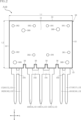
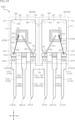
- FIG. 1 is a perspective view showing a semiconductor device according to a first embodiment.
- FIG. 2 is a plan view showing the semiconductor device according to the first embodiment.
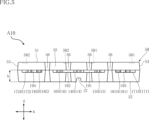
- FIG. 3 is a diagram showing the sealing resin with imaginary lines in the plan view of FIG. 2.
- FIG. 4 is a bottom view showing the semiconductor device according to the first embodiment.
- FIG. 5 is a front view showing the semiconductor device according to the first embodiment.
- FIG. 6 is a right side view showing the semiconductor device according to the first embodiment.
- FIG. 7 is a partial enlarged view of a part of FIG. 6, showing the sealing resin with imaginary lines.
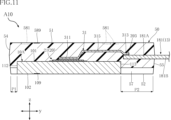
- FIG. 8 is a cross-sectional view taken along line VIII-VIII in FIG. 3.
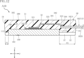
- FIG. 9 is an enlarged view of a part of FIG. 8.
- FIG. 8 is a cross-sectional view taken along line VIII-VIII in FIG. 3.
- FIG. 10 is an enlarged view of a part of FIG. 8.
- FIG. 11 is a cross-sectional view taken along line XI-XI in FIG. 3.
- FIG. 12 is a sectional view taken along line XII-XII in FIG. 3.
- FIG. 13 is a partially enlarged view of FIG. 3.
- FIG. 14 is a partially enlarged view of FIG. 3.
- FIG. 15 is a partial enlarged view of a part of FIG. 3.
- FIG. 16 is a partially enlarged view of FIG. 3.
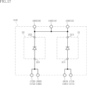
- FIG. 17 is a diagram showing an example of the circuit configuration of the semiconductor device according to the first embodiment.
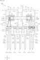
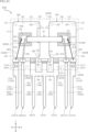
- FIG. 18 is a plan view showing one step in the manufacturing process of the semiconductor device according to the first embodiment.
- FIG. 18 is a plan view showing one step in the manufacturing process of the semiconductor device according to the first embodiment.
- FIG. 19 is a plan view showing a semiconductor device according to a first modification of the first embodiment, in which a sealing resin is shown with imaginary lines.
- FIG. 20 is a plan view showing a semiconductor device according to a second modification of the first embodiment, in which the sealing resin is shown with imaginary lines.
- FIG. 21 is a plan view showing a semiconductor device according to a third modification of the first embodiment, in which the sealing resin is shown with imaginary lines.
- FIG. 22 is a plan view showing the semiconductor device according to the second embodiment, in which the sealing resin is shown with imaginary lines.
- FIG. 23 is a cross-sectional view taken along line XXIII-XXIII in FIG. 22.
- FIG. 24 is an enlarged view of a part of FIG. 23.
- FIG. 25 is a diagram showing an example of the circuit configuration of the semiconductor device according to the second embodiment.
- FIG. 26 is a plan view showing the semiconductor device according to the third embodiment, in which the sealing resin is shown with imaginary lines.
- FIG. 27 is an enlarged cross-sectional view taken along line XXVII-XXVII in FIG. 26.
- FIG. 28 is a diagram showing an example of the circuit configuration of the semiconductor device according to the third embodiment.
- FIG. 29 is a plan view showing the semiconductor device according to the fourth embodiment, in which the sealing resin is shown with imaginary lines.
- FIG. 30 is a diagram showing an example of the circuit configuration of the semiconductor device according to the fourth embodiment.
- FIG. 31 is a plan view showing a semiconductor device according to a first modification of the fourth embodiment, in which a sealing resin is shown with imaginary lines.
- FIG. 32 is a plan view showing a semiconductor device according to a second modification of the fourth embodiment, in which a sealing resin is shown with imaginary lines.
- FIG. 33 is a plan view showing a semiconductor device according to a third modification of the fourth embodiment, in which a sealing resin is shown with imaginary lines.
- a thing A is formed on a thing B" and "a thing A is formed on a thing B” mean “a thing A is formed on a thing B" unless otherwise specified.
- A is formed directly on something B
- a thing A is formed on something B, with another thing interposed between them.” including.
- "a certain thing A is placed on a certain thing B” and "a certain thing A is placed on a certain thing B” are used as "a certain thing A is placed on a certain thing B” unless otherwise specified.
- ⁇ It is placed directly on something B,'' and ⁇ A thing A is placed on something B, with another thing interposed between them.'' include.
- an object A is located on an object B
- an object A is in contact with an object B, and an object A is located on an object B.
- an object A overlaps an object B when viewed in a certain direction means, unless otherwise specified, “an object A overlaps all of an object B" and "a certain object A overlaps an object B".
- a certain thing A (the material of the thing) includes a certain material C” means "a case where the thing A (the material of the thing A) consists of a certain material C" and "the main component of the thing A (the material of the thing)”. "is a certain material C”.
- the semiconductor device A10 includes a first die pad 10A, a second die pad 10B, a plurality of terminal leads 13, a first connection bar 191, a second connection bar 192, a third connection bar 193, a fourth connection bar 194, a semiconductor element 20, and a fourth connection bar 194.
- the first conductive portion 31, the second conductive portion 32, and a sealing resin 50 are provided.
- Semiconductor element 20 includes a first element 21 and a second element 22.
- the plurality of terminal leads 13 include a first terminal lead 14, a second terminal lead 15, a third terminal lead 16, a fourth terminal lead 171, a fifth terminal lead 181, a sixth terminal lead 172, and a seventh terminal lead 182. .
- the thickness direction of the semiconductor device A10 will be referred to as the "thickness direction z.”
- one side of the thickness direction z may be referred to as upper side, and the other side may be referred to as lower side.
- descriptions such as “upper”, “lower”, “upper”, “lower”, “upper surface”, and “lower surface” indicate the relative positional relationship of each component etc. in the thickness direction z, and do not necessarily mean It is not a term that defines the relationship with the direction of gravity.
- “planar view” refers to when viewed in the thickness direction z.
- One direction perpendicular to the thickness direction z is referred to as a "first direction y.”
- a direction perpendicular to the thickness direction z and the first direction y is referred to as a "second direction x.”
- the first die pad 10A and the second die pad 10B are located apart from each other in the second direction x, as shown in FIGS. 3 and 8.
- the first die pad 10A, along with the second die pad 10B and the plurality of terminal leads 13, are configured from the same lead frame.
- the lead frame is made of copper (Cu) or a copper alloy. Therefore, the compositions of the first die pad 10A, the second die pad 10B, and the plurality of terminal leads 13 include copper.
- Each of the first die pad 10A and the second die pad 10B has a rectangular shape in plan view, for example.
- the first die pad 10A and the second die pad 10B each have a main surface 101 and a back surface 102, as shown in FIG.
- the main surface 101 and the back surface 102 described below are common to the first die pad 10A and the second die pad 10B unless otherwise specified.
- the main surface 101 faces in the thickness direction z (upward).
- the main surface 101 is covered with a sealing resin 50.
- the first element 21 is mounted on the main surface 101 of the first die pad 10A.
- the back surface 102 of the first die pad 10A faces the opposite side to the side where the first element 21 is located in the thickness direction z.
- a second element 22 is mounted on the main surface 101 of the second die pad 10B.
- the back surface 102 of the second die pad 10B faces the side opposite to the side where the second element 22 is located in the thickness direction z. As shown in FIGS. 4 and 8, the back surface 102 is exposed from the sealing resin 50.
- the back surface 102 is plated with tin (Sn), for example.
- the sealing resin 50 connects the first element 21, the second element 22, the first conductive part 31, the second conductive part 32, the first die pad 10A, and the second die pad 10B. Further, the sealing resin 50 partially covers each of the plurality of terminal leads 13.
- the sealing resin 50 has electrical insulation properties.
- the sealing resin 50 includes, for example, black epoxy resin. As shown in FIG. 2, the dimension L1 of the sealing resin 50 in the second direction x is longer than the dimension L2 of the sealing resin 50 in the first direction y.
- the sealing resin 50 has a resin main surface 51, a resin back surface 52, a pair of first side surfaces 53, a second side surface 54, a third side surface 55, a plurality of recesses 56, a groove 57, and a plurality of recesses 581, 582.
- the resin main surface 51 faces the same side as each main surface 101 of the first die pad 10A and the second die pad 10B in the thickness direction z.
- the resin back surface 52 faces opposite to the resin main surface 51 in the thickness direction z.
- each back surface 102 of the first die pad 10A and the second die pad 10B is exposed from the resin back surface 52.
- the pair of first side surfaces 53 are located apart from each other in the second direction x.
- the pair of first side surfaces 53 face in the second direction x and extend in the first direction y.
- the pair of first side surfaces 53 are connected to the resin main surface 51 and the resin back surface 52.
- the second side surface 54 and the third side surface 55 are located apart from each other in the first direction y.
- the second side surface 54 and the third side surface 55 face oppositely to each other in the first direction y and extend in the second direction x.
- the second side surface 54 and the third side surface 55 are connected to the resin main surface 51 and the resin back surface 52.
- a plurality of terminal leads 13 are exposed from the third side surface 55.
- the third side surface 55 is an example of a "resin side surface" described in the claims.
- the plurality of recesses 56 are recessed from the third side surface 55 in the first direction y, and extend from the resin main surface 51 to the resin back surface 52 in the thickness direction z. In the second direction They are located individually between the terminal lead 15 and between the second terminal lead 15 and the fifth terminal lead 181.
- the groove portion 57 is recessed from the resin back surface 52 in the thickness direction z and extends along the first direction y. Both sides of the groove portion 57 in the first direction y are connected to the second side surface 54 and the third side surface 55. When viewed along the thickness direction z, the groove portion 57 separates the back surface 102 of the first die pad 10A and the back surface 102 of the second die pad 10B. Note that the sealing resin 50 does not need to have the groove portion 57.
- each of the plurality of recesses 581, 582 is recessed from the main resin surface 51 in the thickness direction z.
- the plan view shape of each of the plurality of recesses 581 and 582 is not particularly limited, in the illustrated example, it is circular.
- each of the plurality of recesses 581 overlaps the first die pad 10A in plan view.
- the plurality of recesses 581 are individually located near the four corners of the first die pad 10A in plan view.
- each of the plurality of recesses 582 overlaps the second die pad 10B in plan view.
- the plurality of recesses 582 are individually located near the four corners of the second die pad 10B in plan view. Each of the plurality of recesses 581 and 582 does not overlap with either the first conductive part 31 or the second conductive part 32 in plan view.
- the plurality of recesses 581 are formed by pins for fixing the first die pad 10A during manufacturing of the semiconductor device A10. The pin is pressed against the first die pad 10A before forming the sealing resin 50, and fixes the first die pad 10A. In this state, formation of the sealing resin 50 is started. Then, the pin is pulled out before the formation of the sealing resin 50 is completed.
- the sealing resin 50 is formed in at least a portion of the area where the pin was arranged, so that the main surface 101 of the first die pad 10A is covered with the sealing resin 50.
- the plurality of recesses 581 are marks formed by such a molding process of the sealing resin 50.
- the plurality of recesses 582 are formed by pins for fixing the second die pad 10B during manufacturing of the semiconductor device A10.
- the plurality of recesses 582 are marks formed by the molding process of the sealing resin 50.
- the sealing resin 50 further has a plurality of traces 589, as shown in FIGS. 1, 2, and 4.
- the plurality of marks 589 are, for example, marks caused by pressing an ejector pin for ejecting the sealing resin 50 from the mold when the sealing resin 50 was formed.
- Each of the plurality of traces 589 is depressed from either the resin main surface 51 or the resin back surface 52. Note that none of the plurality of traces 589 may be formed on the sealing resin 50.
- the back surface 102 of the first die pad 10A and the back surface 102 of the second die pad 10B each have a trace 109.
- the traces 109 formed on the first die pad 10A and the traces 109 formed on the second die pad 10B are traces where the ejector pins described above were pressed.
- the trace 109 formed on the first die pad 10A is depressed from the back surface 102 of the first die pad 10A, and the trace 109 formed on the second die pad 10B is depressed from the back surface 102 of the second die pad 10B. Note that the trace 109 does not need to be formed on either the first die pad 10A or the second die pad 10B.
- the depths of the plurality of traces 589 and the plurality of traces 109 are, for example, smaller than the depths of the plurality of recesses 581, but may be larger or the same.
- the first die pad 10A and the second die pad 10B have a first end surface 111, a second end surface 112, a third end surface 113, and a fourth end surface 114.
- the first end surface 111, the second end surface 112, the third end surface 113, and the fourth end surface 114 are covered with a sealing resin 50.
- the first end surface 111 faces in the second direction x and extends in the first direction y.
- the first end surface 111 is located closest to the pair of first side surfaces 53 of the sealing resin 50.
- the second end surface 112 faces in the first direction y and extends in the second direction x.
- the second end surface 112 is located closest to the second side surface 54 of the sealing resin 50.
- the third end surface 113 faces opposite to the second end surface 112 in the first direction y, and extends in the second direction x.
- the third end surface 113 is located closest to the third side surface 55 of the sealing resin 50.
- the fourth end surface 114 faces opposite to the first end surface 111 in the second direction x, and extends in the first direction y.
- a groove 57 is located between the fourth end surface 114 of the first die pad 10A and the fourth end surface 114 of the second die pad 10B.
- the distance P2 between the third end surface 113 and the third side surface 55 is longer than the distance P1 between the second end surface 112 and the second side surface 54.
- the first die pad 10A and the second die pad 10B have a first corner end surface 121.
- the first corner end surface 121 is located between the first end surface 111 and the second end surface 112, and is located at the corner of either the first die pad 10A or the second die pad 10B.
- the first corner end surface 121 is a plane that is covered with the sealing resin 50 and is inclined with respect to the first end surface 111 and the second end surface 112. Either the first inclination angle ⁇ 1 of the first corner end face 121 with respect to the first end face 111 shown in FIG. 13 and the second inclination angle ⁇ 2 of the first corner end face 121 with respect to the second end face 112 shown in FIG. ° or less. Note that in FIG.
- the first conductive portion 31 is omitted.
- One of the plurality of recesses 581 is located near the first corner end surface 121 of the first die pad 10A in plan view, and one of the plurality of recesses 582 is located near the second die pad 10B in plan view. It is located near the first corner end face 121 of.
- the longest normal line Nmax of the first corner end face 121 is set.
- the longest normal Nmax is the closest from the first corner end surface 121 of either the first die pad 10A or the second die pad 10B to the first corner end surface 121 of the pair of first side surfaces 53 of the sealing resin 50. This is the maximum value of the normal line of the first corner end surface 121 that reaches the first side surface 53 located therein.
- the longest normal Nmax is 1.0 times or more the length of the intersection line C (see FIG. 13) between the first corner end surface 121 and a virtual plane whose in-plane directions are the first direction y and the second direction x. It is 1.5 times or less.
- the first die pad 10A and the second die pad 10B have a second corner end surface 122.
- the second corner end surface 122 is located between the first end surface 111 and the third end surface 113, and is located at the corner of either the first die pad 10A or the second die pad 10B.
- the second corner end surface 122 is a plane that is covered with the sealing resin 50 and is inclined with respect to the first end surface 111 and the third end surface 113. Either the third inclination angle ⁇ 3 of the second corner end face 122 with respect to the first end face 111 shown in FIG. 14 or the fourth inclination angle ⁇ 4 of the second corner end face 122 with respect to the third end face 113 shown in FIG. ° or less.
- One of the plurality of recesses 581 is located near the second corner end surface 122 of the first die pad 10A in a plan view, and one of the plurality of recesses 582 is located near the second die pad 10B in a plan view. It is located near the second corner end face 122 of.
- the first die pad 10A and the second die pad 10B have a third corner end surface 123.
- the third corner end surface 123 is located between the second end surface 112 and the fourth end surface 114, and is located at the corner of either the first die pad 10A or the second die pad 10B.
- the third corner end surface 123 is a plane that is covered with the sealing resin 50 and is inclined with respect to the second end surface 112 and the fourth end surface 114. Either the fifth inclination angle ⁇ 5 of the third corner end face 123 with respect to the fourth end face 114 and the sixth inclination angle ⁇ 6 of the third corner end face 123 with respect to the second end face 112 shown in FIG. ° or less.
- One of the plurality of recesses 581 is located near the third corner end surface 123 of the first die pad 10A in plan view, and one of the plurality of recesses 582 is located near the second die pad 10B in plan view. It is located near the third corner end face 123 of.
- the first die pad 10A and the second die pad 10B have a fourth corner end surface 124.
- the fourth corner end surface 124 is located between the third end surface 113 and the fourth end surface 114, and is located at the corner of either the first die pad 10A or the second die pad 10B.
- the fourth corner end surface 124 is a plane that is covered with the sealing resin 50 and is inclined with respect to the third end surface 113 and the fourth end surface 114. Either the seventh inclination angle ⁇ 7 of the fourth corner end face 124 with respect to the fourth end face 114 and the eighth inclination angle ⁇ 8 of the fourth corner end face 124 with respect to the third end face 113 shown in FIG. ° or less.
- One of the plurality of recesses 581 is located near the fourth corner end surface 124 of the first die pad 10A in plan view, and one of the plurality of recesses 582 is located near the second die pad 10B in plan view. It is located near the fourth corner end face 124 of.
- the semiconductor element 20 is the functional center of the semiconductor device A10.
- Semiconductor element 20 includes a first element 21 and a second element 22.
- the first element 21 and the second element 22 are individually formed chips. As shown in FIG. 17, in the semiconductor device A10, the first element 21 and the second element 22 are, for example, diodes.
- Each of the first element 21 and the second element 22 includes a compound semiconductor substrate.
- the composition of the compound semiconductor substrate includes silicon (Si) or silicon carbide (SiC).
- the first element 21 is mounted on the first die pad 10A, as shown in FIGS. 3, 8, and 9.
- the center of gravity of the first element 21 overlaps the center of the first die pad 10A in plan view.
- the center of the first die pad 10A is the center when the first die pad 10A is divided into Nx (Nx is a positive odd number) in the second direction x, and the center of the first die pad 10A is divided into Ny (Ny is a positive odd number) This is the area corresponding to the center when divided.
- Nx and Ny are each 3 or 5, for example, although they are not limited in any way.
- the first element 21 has a first main surface 21a and a first back surface 21b.
- the first main surface 21a and the first back surface 21b are spaced apart from each other in the thickness direction z.
- the first main surface 21a faces the same direction as the main surface 101 of the first die pad 10A.
- the first back surface 21b faces opposite to the first main surface 21a in the thickness direction z, and faces the main surface 101 of the first die pad 10A.
- the first element 21 has a main surface electrode 211 and a back surface electrode 213.
- the main surface electrode 211 is arranged on the first main surface 21a, as shown in FIG.
- the main surface electrode 211 is, for example, an anode electrode.
- Main surface electrode 211 includes multiple metal plating layers.
- Main surface electrode 211 includes a nickel (Ni) plating layer and a gold (Au) plating layer laminated on the nickel plating layer.
- the main surface electrode 211 may include a nickel plating layer, a palladium (Pd) plating layer laminated on the nickel plating layer, and a gold plating layer laminated on the palladium plating layer. .
- the back electrode 213 is arranged on the first back surface 21b, as shown in FIG.
- the back electrode 213 is provided facing the main surface 101 of the first die pad 10A.
- the back electrode 213 is, for example, a cathode electrode.
- the second element 22 is mounted on the main surface 101 of the second die pad 10B, as shown in FIGS. 3, 8, and 10.
- the center of gravity of the second element 22 overlaps the center of the second die pad 10B in plan view.
- the center of the second die pad 10B is the center when the second die pad 10B is divided into Lx (Lx is a positive odd number) in the second direction x, and the center of the second die pad 10B is divided into Ly (Ly) in the first direction y. is a positive odd number) This is the area corresponding to the center when divided.
- Lx and Ly are each 3 or 5, for example, although there are no limitations.
- the second element 22 has a second main surface 22a and a second back surface 22b.
- the second main surface 22a and the second back surface 22b are spaced apart from each other in the thickness direction z.
- the second main surface 22a faces the same direction as the main surface 101 of the second die pad 10B.
- the second back surface 22b faces the opposite side from the second main surface 22a in the thickness direction z, and faces the main surface 101 of the second die pad 10B.
- the second element 22 has a main surface electrode 221 and a back surface electrode 223.
- the main surface electrode 221 is arranged on the second main surface 22a, as shown in FIG.
- the main surface electrode 221 is, for example, an anode electrode.
- the main surface electrode 221 includes a plurality of metal plating layers.
- the main surface electrode 221 includes a nickel (Ni) plating layer and a gold (Au) plating layer laminated on the nickel plating layer.
- the main surface electrode 221 may include a nickel plating layer, a palladium (Pd) plating layer laminated on the nickel plating layer, and a gold plating layer laminated on the palladium plating layer. .
- the back electrode 223 is arranged on the second back surface 22b, as shown in FIG. Back electrode 223 is provided facing main surface 101 of second die pad 10B.
- the back electrode 223 is, for example, a cathode electrode.
- the semiconductor device A10 further includes two die bonding layers 231 and 232, as shown in FIG. 3 and FIGS. 8 to 10.
- Each of the two die bonding layers 231 and 232 has conductivity.
- Each die bonding layer 231, 232 is, for example, solder.
- each die bonding layer 231, 232 may be made of sintered metal.
- the die bonding layer 231 is interposed between the main surface 101 of the first die pad 10A and the back electrode 213 of the first element 21, as shown in FIGS. 8 and 9.
- the die bonding layer 231 bonds the main surface 101 of the first die pad 10A and the back electrode 213 of the first element 21.
- the back electrode 213 of the first element 21 is electrically connected to the first die pad 10A.
- the die bonding layer 232 is interposed between the main surface 101 of the second die pad 10B and the back electrode 223 of the second element 22, as shown in FIGS. 8 and 10.
- the die bonding layer 232 bonds the main surface 101 of the second die pad 10B and the back electrode 223 of the second element 22. Thereby, the back electrode 223 of the second element 22 is electrically connected to the second die pad 10B.
- the plurality of terminal leads 13 are located on the opposite side of the first die pad 10A and the second die pad 10B from the side where the second end surface 112 faces in the first direction y. At least one of the plurality of terminal leads 13 is electrically connected to either the first element 21 or the second element 22.
- the plurality of terminal leads 13 are arranged along the second direction x.
- the plurality of terminal leads 13 include a first terminal lead 14, a second terminal lead 15, a third terminal lead 16, a fourth terminal lead 171, a fifth terminal lead 181, a sixth terminal lead 172, and a seventh terminal lead 182. .
- the first terminal lead 14 is separated from the first die pad 10A and the second die pad 10B in the first direction y.
- the first terminal lead 14 is located between the second terminal lead 15 and the third terminal lead 16 in the second direction x.
- the first terminal lead 14 extends along the first direction y.
- the first terminal lead 14 is electrically connected to the main surface electrode 211 (anode electrode) of the first element 21 and the main surface electrode 221 (anode electrode) of the second element 22.
- the first terminal lead 14 includes a first inner part 14A and a first outer part 14B. As shown in FIG. 3, the first inner part 14A is covered with a sealing resin 50. As shown in FIG. 3, the first outer part 14B is connected to the first inner part 14A and exposed from the third side surface 55 of the sealing resin 50. The first outer portion 14B extends away from the first die pad 10A and the second die pad 10B in the first direction y. The surface of the first outer portion 14B is plated with tin, for example.
- the first outer portion 14B includes a first base end portion 141 and a first distal end portion 142, as shown in FIG.
- the first base end portion 141 extends from the third side surface 55 in the first direction y.
- the first distal end portion 142 extends from the first base end portion 141 in the first direction y.
- the width of the first distal end portion 142 (dimension along the second direction x) is smaller than the width of the first proximal end portion 141 (dimension along the second direction x).
- the second terminal lead 15 includes a portion extending along the first direction y, and is connected to the first die pad 10A. Therefore, the second terminal lead 15 is electrically connected to the back electrode 213 (cathode electrode) of the first element 21 via the first die pad 10A.
- the second terminal lead 15 includes a second inner part 15A and a second outer part 15B.
- the second inner portion 15A is connected to the third end surface 113 of the first die pad 10A, and is covered with the sealing resin 50.
- the second inner portion 15A is bent when viewed along the second direction x.
- the second outer portion 15B is connected to the second inner portion 15A and exposed from the third side surface 55 of the sealing resin 50.
- the second outer portion 15B extends away from the first die pad 10A in the first direction y.
- the second outer portion 15B is adjacent to the first outer portion 14B on one side in the second direction x.
- the surface of the second outer portion 15B is plated with tin, for example.
- the second outer portion 15B includes a second base end portion 151 and a second tip end portion 152, as shown in FIG.
- the second base end portion 151 extends from the third side surface 55 in the first direction y.
- the second distal end portion 152 extends from the second base end portion 151 in the first direction y.
- the width of the second tip portion 152 (the dimension along the second direction x) is smaller than the width of the second base end portion 151 (the dimension along the second direction x).
- the third terminal lead 16 includes a portion extending along the first direction y, and is connected to the second die pad 10B. Therefore, the third terminal lead 16 is electrically connected to the back electrode 223 (cathode electrode) of the second element 22 via the second die pad 10B.
- the third terminal lead 16 includes a third inner part 16A and a third outer part 16B.
- the third inner portion 16A is connected to the third end surface 113 of the second die pad 10B and is covered with the sealing resin 50.
- the third inner portion 16A is bent similarly to the second inner portion 15A of the second terminal lead 15.
- the third outer part 16B is connected to the third inner part 16A and exposed from the third side surface 55 of the sealing resin 50.
- the third outer portion 16B extends away from the second die pad 10B in the first direction y.
- the third outer portion 16B is adjacent to the first outer portion 14B on the other side in the second direction x.
- the surface of the third outer portion 16B is plated with tin, for example.
- the third outer portion 16B includes a third base end portion 161 and a third distal end portion 162, as shown in FIG.
- the third base end portion 161 extends from the third side surface 55 in the first direction y.
- the third distal end portion 162 extends from the third base end portion 161 in the first direction y.
- the width of the third distal end portion 162 (dimension along the second direction x) is smaller than the width of the third proximal end portion 161 (dimension along the second direction x).
- the fourth terminal lead 171 is separated from the first die pad 10A in the first direction y.
- the fourth terminal lead 171 is located closest to one side in the second direction x among the plurality of terminal leads 13.
- the fourth terminal lead 171 is electrically connected to the main surface electrode 211 (anode electrode) of the first element 21 .
- the fourth terminal lead 171 includes a fourth inner part 171A and a fourth outer part 171B.
- the fourth inner portion 171A is covered with a sealing resin 50.
- the fourth outer part 171B is connected to the fourth inner part 171A and exposed from the third side surface 55 of the sealing resin 50.
- the fourth outer portion 171B extends away from the first die pad 10A in the first direction y.
- the surface of the fourth outer portion 171B is plated with tin, for example.
- the fourth outer portion 171B includes a fourth base end portion 1711 and a fourth distal end portion 1712, as shown in FIG.
- the fourth base end portion 1711 extends from the third side surface 55 in the first direction y.
- the fourth distal end portion 1712 extends from the fourth base end portion 1711 in the first direction y.
- the width of the fourth distal end portion 1712 (dimension along the second direction x) is smaller than the width of the fourth proximal end portion 1711 (dimension along the second direction x).
- the fifth terminal lead 181 is separated from the first die pad 10A in the first direction y.
- the fifth terminal lead 181 is located between the second terminal lead 15 and the fourth terminal lead 171 in the second direction x.
- the fifth terminal lead 181 is electrically connected to the main surface electrode 211 (anode electrode) of the first element 21 .
- the fifth terminal lead 181 includes a fifth inner part 181A and a fifth outer part 181B.
- the fifth inner portion 181A is covered with a sealing resin 50.
- the fifth outer part 181B is connected to the fifth inner part 181A and exposed from the third side surface 55 of the sealing resin 50.
- the fifth outer portion 181B extends away from the first die pad 10A in the first direction y.
- the surface of the fifth outer portion 181B is plated with tin, for example.
- the fifth terminal lead 181 includes a fifth base end 1811 and a fifth distal end 1812, as shown in FIG.
- the fifth base end portion 1811 extends from the third side surface 55 in the first direction y.
- the fifth distal end portion 1812 extends from the fifth base end portion 1811 in the first direction y.
- the width of the fifth distal end 1812 (dimension along the second direction x) is the same (or approximately the same) as the width of the fifth proximal end 1811 (dimension along the second direction x). .
- the width of the fifth proximal end 1811 and the width of the fifth distal end 1812 may be different.
- the sixth terminal lead 172 is separated from the second die pad 10B in the first direction y.
- the sixth terminal lead 172 is located closest to the other side in the second direction x among the plurality of terminal leads 13.
- the sixth terminal lead 172 is electrically connected to the main surface electrode 222 (anode electrode) of the second element 22.
- the sixth terminal lead 172 includes a sixth inner part 172A and a sixth outer part 172B.
- the sixth inner portion 172A is covered with a sealing resin 50.
- the sixth outer portion 172B is connected to the sixth inner portion 172A and exposed from the sealing resin 50.
- the sixth outer portion 172B extends away from the second die pad 10B in the first direction y.
- the surface of the sixth outer portion 172B is plated with tin, for example.
- the sixth terminal lead 172 includes a sixth base end 1721 and a sixth distal end 1722, as shown in FIG.
- the sixth base end portion 1721 extends from the third side surface 55 in the first direction y.
- the sixth distal end portion 1722 extends from the sixth base end portion 1721 in the first direction y.
- the width of the sixth distal end portion 1722 (dimension along the second direction x) is smaller than the width of the sixth proximal end portion 1721 (dimension along the second direction x).
- the seventh terminal lead 182 is separated from the second die pad 10B in the first direction y.
- the seventh terminal lead 182 is located between the third terminal lead 16 and the sixth terminal lead 172 in the second direction x.
- the seventh terminal lead 182 is electrically connected to the main surface electrode 221 (anode electrode) of the second element 22.
- the seventh terminal lead 182 includes a seventh inner part 182A and a seventh outer part 182B.
- the seventh inner portion 182A is covered with a sealing resin 50.
- the seventh outer part 182B is connected to the seventh inner part 182A and exposed from the third side surface 55 of the sealing resin 50.
- the seventh outer portion 182B extends away from the second die pad 10B in the first direction y.
- the surface of the seventh outer portion 182B is plated with tin, for example.
- the seventh terminal lead 182 includes a seventh base end 1821 and a seventh distal end 1822, as shown in FIG.
- the seventh base end portion 1821 extends from the third side surface 55 in the first direction y.
- the seventh tip portion 1822 extends from the seventh base portion 1821 in the first direction y.
- the width of the seventh distal end 1822 (dimension along the second direction x) is the same (or approximately the same) as the width of the seventh proximal end 1821 (dimension along the second direction x). .
- the width of the seventh proximal end 1821 and the width of the seventh distal end 1822 may be different.
- each height h of the outer portion 182B is the same. Furthermore, each of these thicknesses are the same. Therefore, when viewed along the second direction The seven outer portions 182B overlap each other (see FIG. 6).
- the first connection bar 191 is separated from the sealing resin 50, as shown in FIGS. 2 and 3.
- the first connection bar 191 is sandwiched between the first outer part 14B and the second outer part 15B in the second direction x.
- the first connection bar 191 is integrally formed with the first outer part 14B and the second outer part 15B.
- the first connection bar 191 is connected to the first base end 141 of the first outer part 14B and to the second base end 151 of the second outer part 15B.
- the first tip portion 142 and the second tip portion 152 extend further to one side in the first direction y than the first connection bar 191.
- the second connection bar 192 is separated from the sealing resin 50, as shown in FIGS. 2 and 3.
- the second connection bar 192 is sandwiched between the first outer part 14B and the third outer part 16B in the second direction x.
- the second connection bar 192 is integrally formed with the first outer section 14B and the third outer section 16B.
- the second connection bar 192 is connected to the first base end portion 141 of the first outer portion 14B, and also to the third base end portion 161 of the third outer portion 16B.
- the first tip portion 142 and the third tip portion 162 extend further to one side in the first direction y than the second connection bar 192.
- the second connection bar 192 overlaps the first connection bar 191 when viewed along the second direction x.
- the third connection bar 193 is separated from the sealing resin 50, as shown in FIGS. 2 and 3.
- the third connection bar 193 is sandwiched between the fourth outer part 171B and the fifth outer part 181B in the second direction x.
- the third connection bar 193 is integrally formed with the fourth outer part 171B and the fifth outer part 181B.
- the third connection bar 193 is connected to the fourth base end 1711 of the fourth outer part 171B, and also connected to the fifth base end 1811 of the fifth outer part 181B.
- the fourth tip portion 1712 and the fifth tip portion 1812 extend further to one side in the first direction y than the third connection bar 193.
- the third connection bar 193 overlaps each of the first connection bar 191 and the second connection bar 192 when viewed along the second direction x.
- the fourth connection bar 194 is separated from the sealing resin 50, as shown in FIG.
- the fourth connection bar 194 is sandwiched between the sixth outer part 172B and the seventh outer part 182B in the second direction x.
- the fourth connection bar 194 is integrally formed with the sixth outer part 172B and the seventh outer part 182B.
- the fourth connection bar 194 is connected to the sixth base end 1721 of the sixth outer part 172B, and also to the seventh base end 1821 of the seventh outer part 182B.
- the sixth tip portion 1722 and the seventh tip portion 1822 extend further to one side in the first direction y than the fourth connection bar 194.
- the fourth connection bar 194 overlaps each of the first connection bar 191, the second connection bar 192, and the third connection bar 193 when viewed along the second direction x.
- the first conductive portion 31 connects the main surface electrode 211 of the first element 21, the fourth terminal lead 171, and the fifth terminal lead 181 to each other.
- the first conductive portion 31 is a metal plate.
- the first conductive portion 31 is a metal clip.
- the composition of the first conductive portion 31 includes copper, for example.
- the first conductive portion 31 is covered with a sealing resin 50.
- the first conductive section 31 includes three joining sections 311, 312, 313 and two connecting sections 314, 315.
- the bonding portion 311 is bonded to the main surface electrode 211 of the first element 21, as shown in FIGS. 3, 8, and 9.
- the joint portion 311 has a rectangular shape in plan view.
- the area of the joint portion 311 in plan view is, for example, 10% or more and 100% or less of the area of main surface electrode 211 in plan view.
- the joint portion 312 is joined to the fourth inner portion 171A of the fourth terminal lead 171, as shown in FIG.
- the joint portion 312 has a rectangular shape in plan view.
- the joint portion 313 is joined to the fifth inner portion 181A of the fifth terminal lead 181, as shown in FIGS. 3 and 11.
- the joint portion 313 has a rectangular shape in plan view.
- the connecting portion 314 is connected to the joint portion 311 and the joint portion 312, as shown in FIG.
- the connecting portion 314 is strip-shaped in plan view.
- the connecting portion 314 extends linearly from the joint portion 311 to the joint portion 312 in a plan view.
- the end portion on the side connected to the joint portion 311 and the end portion on the side connected to the joint portion 312 are each bent downward in the thickness direction z.
- the connecting portion 315 is connected to the joining portion 311 and the joining portion 313, as shown in FIGS. 3 and 11.
- the connecting portion 315 is strip-shaped in plan view.
- the connecting portion 315 extends linearly from the joining portion 311 to the joining portion 313.
- the end portion on the side connected to the joint portion 311 and the end portion on the side connected to the joint portion 313 are each bent downward in the thickness direction z.
- the two connecting parts 314, 315 each have a bent portion as described above. Unlike this configuration, in the following case, each of the two connecting portions 314 and 315 does not need to have a bent portion in the thickness direction z.
- the two joint parts 314, 315 each have a bent part in the thickness direction z. It doesn't have to be.
- the two connecting parts 314 and 315 are arranged at the same height in the thickness direction z. It is not necessary to have a portion bent in the z direction.
- the first conductive portion 31 is a flat plate.
- the second conductive portion 32 connects the main surface electrode 221 of the second element 22, the sixth terminal lead 172, and the seventh terminal lead 182 to each other.
- the second conductive portion 32 is a metal plate.
- the second conductive portion 32 is a metal clip.
- the composition of the second conductive portion 32 includes copper, for example.
- the second conductive portion 32 is covered with a sealing resin 50.
- the second conductive portion 32 includes three joining portions 321, 322, 323 and two connecting portions 324, 325.
- the bonding portion 321 is bonded to the main surface electrode 221 of the second element 22, as shown in FIGS. 3, 8, and 10.
- the joint portion 321 has a rectangular shape in plan view.
- the area of the joint portion 321 in plan view is, for example, 10% or more and 100% or less of the area of main surface electrode 222 in plan view.
- the joint portion 322 is joined to the sixth inner portion 172A of the sixth terminal lead 172.
- the joint portion 322 has a rectangular shape in plan view.
- the joint portion 323 is joined to the seventh inner portion 182A of the seventh terminal lead 182, as shown in FIGS. 3 and 12.
- the joint portion 323 has a rectangular shape in plan view.
- the connecting portion 324 is connected to the joint portion 321 and the joint portion 322, as shown in FIG.
- the connecting portion 324 is strip-shaped in plan view.
- the connecting portion 324 extends linearly from the joint portion 321 to the joint portion 322 in a plan view.
- the end portion on the side connected to the joint portion 321 and the end portion on the side connected to the joint portion 322 are each bent downward in the thickness direction z.
- the connecting portion 325 is connected to the joining portion 321 and the joining portion 323, as shown in FIGS. 3 and 12.
- the connecting portion 325 is strip-shaped in plan view.
- the connecting portion 325 extends linearly from the joint portion 321 to the joint portion 323 in a plan view.
- the end portion on the side connected to the joint portion 321 and the end portion on the side connected to the joint portion 323 are each bent downward in the thickness direction z.
- the two connecting parts 324 , 325 each have a bent portion as described above. Unlike this configuration, in the following case, the two connecting portions 324 and 325 each have a configuration that does not have a bent portion in the thickness direction z.
- the two connection parts 324, 325 each have a bent part in the thickness direction z. You don't have to.
- the two connecting parts 324, 325 may not have a bent portion in the thickness direction z.
- the second conductive portion 32 is a flat plate.
- the semiconductor device A10 further includes a plurality of bonding layers 391, 392, 393, and 394, as shown in FIG. 3 and FIGS. 8 to 12.
- Each of the plurality of bonding layers 391, 392, 393, and 394 is electrically conductive.
- Each of the plurality of bonding layers 391, 392, 393, and 394 is made of, for example, solder, but may also be made of sintered metal.
- the bonding layer 391 is interposed between the main surface electrode 211 of the first element 21 and the bonding portion 311 of the first conductive portion 31.
- the bonding layer 391 electrically connects the main surface electrode 211 and the bonding portion 311.
- the bonding layer 392 is interposed between the main surface electrode 221 of the second element 22 and the bonding portion 321 of the second conductive portion 32.
- the bonding layer 392 electrically connects the main surface electrode 221 and the bonding portion 321.
- one of the two bonding layers 393 is interposed between the bonding portion 312 of the first conductive portion 31 and the fourth inner portion 171A.
- the bonding layer 393 electrically connects the bonding portion 312 and the fourth inner portion 171A.
- the other of the two bonding layers 393 is interposed between the bonding portion 313 of the first conductive portion 31 and the fifth inner portion 181A.
- the bonding layer 393 electrically connects the bonding portion 313 and the fifth inner portion 181A.
- one of the two bonding layers 394 is interposed between the bonding portion 322 of the second conductive portion 32 and the sixth inner portion 172A.
- the bonding layer 394 electrically connects the bonding portion 322 and the sixth inner portion 172A.
- the other of the two bonding layers 394 is interposed between the bonding portion 323 of the second conductive portion 32 and the seventh inner portion 182A.
- the bonding layer 394 electrically connects the bonding portion 323 and the seventh inner portion 182A.
- the thickness t1 (see FIG. 9) of the bonding portion 311 is 0.1 mm or more and less than twice the maximum thickness T1max (see FIG. 9) of the bonding layer 391.
- the maximum thickness T1max of the bonding layer 391 is greater than the thickness of the first element 21.
- the thickness t2 (see FIG. 10) of the bonding portion 321 is at least 0.1 mm and at most twice the maximum thickness T2max (see FIG. 10) of the bonding layer 392.
- the maximum thickness T2max of the bonding layer 392 is greater than the thickness of the second element 22. Note that, for example, the thickness t1 of the joint portion 311 and the thickness t2 of the joint portion 321 have the same value.
- the first outer section 14B, the second outer section 15B, the third outer section 16B, the fourth outer section 171B, the fifth outer section 181B, the sixth outer section 172B, and the seventh outer section 182B are each made of a semiconductor.
- This is a mounting terminal for mounting the device A10 on a circuit board.
- the first outer part 14B, the second outer part 15B, and the third outer part 16B are mounting terminals that are electrically connected to both the back electrode 213 of the first element 21 and the back electrode 223 of the second element 22.
- the fourth outer portion 171B and the fifth outer portion 181B are each a mounting terminal electrically connected to the main surface electrode 211 of the first element 21.
- the sixth outer portion 172B and the seventh outer portion 182B are each a mounting terminal electrically connected to the main surface electrode 221 of the second element 22.
- the first inner part 14A is electrically connected to the back electrode 213 of the first element 21 and the back electrode 223 of the second element 22 through the first outer part 14B. That is, the first inner part 14A is electrically connected to each of the back electrode 213 and the back electrode 223 via the first outer part 14B. Specifically, the first inner part 14A connects to the first element 21 via the first outer part 14B, the first connection bar 191, the second outer part 15B, the second inner part 15A, and the first die pad 10A. It is electrically connected to the back electrode 213 of.
- first inner part 14A connects the back surface electrode of the second element 22 via the first outer part 14B, the second connection bar 192, the third outer part 16B, the third inner part 16A, and the second die pad 10B. 223 is electrically connected.
- the conductive paths from the first inner part 14A to each of the back electrode 213 and the back electrode 223 are not connected only inside the sealing resin 50, but pass outside the sealing resin 50.
- the second inner part 15A is electrically connected to the back electrode 213 of the first element 21 without passing through the second outer part 15B. That is, the second inner part 15A is electrically connected to the back electrode 213 of the first element 21 without going through the second outer part 15B. Specifically, the second inner portion 15A is electrically connected to the back electrode 213 of the first element 21 via the first die pad 10A. On the other hand, the second inner part 15A is electrically connected to the back electrode 223 of the second element 22 through the second outer part 15B. That is, the second inner part 15A is electrically connected to the back electrode 223 of the second element 22 via the second outer part 15B.
- the second inner part 15A includes a second outer part 15B, a first connection bar 191, a first outer part 14B, a second connection bar 192, a third outer part 16B, a third inner part 16A, and a second It is electrically connected to the back electrode 223 of the second element 22 via the die pad 10B.
- the conductive path from the second inner portion 15A to the back electrode 213 is connected only inside the sealing resin 50.
- the conductive path from the second inner part 15A to the back electrode 223 is not connected only inside the sealing resin 50, but passes outside the sealing resin 50.
- the third inner part 16A is electrically connected to the back electrode 223 of the second element 22 without passing through the third outer part 16B. That is, the third inner part 16A is electrically connected to the back electrode 223 of the second element 22 without going through the third outer part 16B. Specifically, the third inner portion 16A is electrically connected to the back electrode 223 of the second element 22 via the second die pad 10B. On the other hand, the third inner part 16A is electrically connected to the back electrode 213 of the first element 21 through the third outer part 16B. That is, the third inner part 16A is electrically connected to the back electrode 213 of the first element 21 via the third outer part 16B.
- the third inner part 16A includes a third outer part 16B, a second connection bar 192, a first outer part 14B, a first connection bar 191, a second outer part 15B, a second inner part 15A, and a first It is electrically connected to the back electrode 213 of the first element 21 via the die pad 10A.
- the conductive path from the third inner portion 16A to the back electrode 213 is not connected only inside the sealing resin 50, but passes outside the sealing resin 50.
- the conductive path from the third inner portion 16A to the back electrode 223 is connected only inside the sealing resin 50.
- the semiconductor device A10 in the conduction between the fourth inner part 171A and the main surface electrode 211 of the first element 21, the semiconductor device A10 has a path that does not go through the fourth outer part 171B. In this path, the fourth inner portion 171A is electrically connected to the main surface electrode 211 via a portion of the first conductive portion 31 (the joint portion 312, the connecting portion 314, and the joint portion 311). Furthermore, as shown in FIG. 3, the semiconductor device A10 also has a path via the fourth outer part 171B for electrical connection between the fourth inner part 171A and the main surface electrode 211 of the first element 21.
- the fourth inner part 171A connects the fourth outer part 171B, the third connection bar 193, the fifth outer part 181B, the fifth inner part 181A, and a part of the first conductive part 31 (joint part 313, It is electrically connected to the main surface electrode 211 via the connecting portion 315 and the joint portion 311).
- the semiconductor device A10 in the conduction between the fifth inner part 181A and the main surface electrode 211 of the first element 21, the semiconductor device A10 has a path that does not go through the fifth outer part 181B.
- the fifth inner portion 181A is electrically connected to the main surface electrode 211 via a portion of the first conductive portion 31 (the joint portion 313, the connecting portion 315, and the joint portion 311).
- the semiconductor device A10 also has a path via the fifth outer part 181B for electrical connection between the fifth inner part 181A and the main surface electrode 211 of the first element 21.
- the fifth inner part 181A connects the fifth outer part 181B, the third connection bar 193, the fourth outer part 171B, the fourth inner part 171A, and a part of the first conductive part 31 (joint part 312, It is electrically connected to the main surface electrode 211 via the connecting portion 314 and the joint portion 311).
- the semiconductor device A10 in the conduction between the sixth inner part 172A and the main surface electrode 221 of the second element 22, the semiconductor device A10 has a path that does not go through the sixth outer part 172B.
- the sixth inner portion 172A is electrically connected to the main surface electrode 221 via a portion of the second conductive portion 32 (the joint portion 322, the connecting portion 324, and the joint portion 321).
- the semiconductor device A10 also has a path via the sixth outer part 172B for electrical connection between the sixth inner part 172A and the main surface electrode 221 of the second element 22.
- the sixth inner part 172A connects the sixth outer part 172B, the fourth connection bar 194, the seventh outer part 182B, the seventh inner part 182A, and a part of the second conductive part 32 (joint part 323, It is electrically connected to the main surface electrode 221 via the connecting portion 325 and the joint portion 321).
- the semiconductor device A10 in the conduction between the seventh inner part 182A and the main surface electrode 221 of the second element 22, the semiconductor device A10 has a path that does not go through the seventh outer part 182B.
- the seventh inner portion 182A is electrically connected to the main surface electrode 221 via a portion of the second conductive portion 32 (the joint portion 323, the connecting portion 325, and the joint portion 321).
- the semiconductor device A10 also has a path via the seventh outer part 182B for electrical connection between the seventh inner part 182A and the main surface electrode 221 of the second element 22.
- the seventh inner part 182A connects the seventh outer part 182B, the fourth connection bar 194, the sixth outer part 172B, the sixth inner part 172A, and a part of the second conductive part 32 (joint part 322, It is electrically connected to the main surface electrode 221 via the connecting portion 324 and the joint portion 321).
- the semiconductor device A10 in the semiconductor device A10 configured as above, as shown in FIG. 17, the back electrode 213 of the first element 21 and the back electrode 223 of the second element 22 are electrically connected to each other. Therefore, in this embodiment, the semiconductor device A10 constitutes a circuit in which the cathode electrodes of two diodes are connected in common (a circuit in which the cathodes are connected in common).
- the functions and effects of the semiconductor device A10 according to the first embodiment are as follows.
- the semiconductor device A10 includes a first terminal lead 14, a second terminal lead 15, a first connection bar 191, and a sealing resin 50.
- the sealing resin 50 has a third side surface 55.
- the first terminal lead 14 includes a first outer portion 14B protruding from the third side surface 55
- the second terminal lead 15 includes a second outer portion 15B protruding from the third side surface 55.
- the first connecting bar 191 is integrally connected to the first outer part 14B and the second outer part 15B.
- FIG. 18 shows one step in the manufacturing process of the semiconductor device A10. In the state shown in FIG. 18, a plurality of semiconductor devices A10 that are being manufactured are connected to each other by tie bars 99. In the state shown in FIG. In the state shown in FIG.
- the semiconductor device A10 is manufactured by cutting the portion of the tie bar 99 shown by hatching (dot drawing). Therefore, the first connection bar 191 is a portion of the tie bar 99 that remains. Therefore, the semiconductor device A10 can effectively utilize the tie bar 99 to electrically connect the first terminal lead 14 and the second terminal lead 15.
- the semiconductor device A10 further includes a third terminal lead 16 and a second connection bar 192.
- the third terminal lead 16 includes a third outer portion 16B protruding from the third side surface 55.
- the second connecting bar 192 is integrally connected to the first outer section 14B and the third outer section 16B. As understood from FIG. 18, the second connection bar 192 is a portion of the tie bar 99 that remains. Therefore, the semiconductor device A10 can effectively utilize the tie bar 99 to electrically connect the first terminal lead 14 and the third terminal lead 16.
- the semiconductor device A10 includes a fourth terminal lead 171, a fifth terminal lead 181, and a third connection bar 193.
- the fourth terminal lead 171 includes a fourth outer portion 171B protruding from the third side surface 55
- the fifth terminal lead 181 includes a fifth outer portion 181B protruding from the third side surface 55.
- the third connection bar 193 is integrally connected to the fourth outer part 171B and the fifth outer part 181B. As understood from FIG. 18, the third connection bar 193 is a portion of the tie bar 99 that remains. Therefore, the semiconductor device A10 can effectively utilize the tie bar 99 to electrically connect the fourth terminal lead 171 and the fifth terminal lead 181.
- the semiconductor device A10 includes a sixth terminal lead 172, a seventh terminal lead 182, and a fourth connection bar 194.
- the sixth terminal lead 172 includes a sixth outer portion 172B protruding from the third side surface 55
- the seventh terminal lead 182 includes a seventh outer portion 182B protruding from the third side surface 55.
- the fourth connection bar 194 is integrally connected to the sixth outer section 172B and the seventh outer section 182B. As understood from FIG. 18, the fourth connecting bar 194 is a portion of the tie bar 99 that remains. Therefore, the semiconductor device A10 can effectively utilize the tie bar 99 to electrically connect the sixth terminal lead 172 and the seventh terminal lead 182.
- the semiconductor element 20 includes a first element 21 and a second element 22.
- the first element 21 and the second element 22 are covered with a sealing resin 50.
- the first element 21 and the second element 22 are packaged with one sealing resin 50. Therefore, the semiconductor device A10 can reduce the mounting area on the circuit board on which the semiconductor device A10 is mounted.
- the first terminal lead 14, the second terminal lead 15, and the third terminal lead 16 are electrically connected to the back electrode 213 of the first element 21 and the back electrode 223 of the second element 22.
- the first terminal lead 14, the second terminal lead 15, and the third terminal lead 16 serve as common terminals for the back electrode 213 of the first element 21 and the back electrode 223 of the second element 22.
- the semiconductor device A10 forms a circuit with common cathodes. In other words, in the semiconductor device A10, a circuit in which two diodes are connected to common cathodes can be packaged into one package.
- the fourth inner part 171A is electrically connected to the main surface electrode 211 of the first element 21 through a part of the first conductive part 31 (junction part 311, junction part 312, and connection part 314), and The inner portion 181A is electrically connected to the main surface electrode 211 of the first element 21 through a portion of the first conductive portion 31 (the joint portion 311, the joint portion 313, and the connecting portion 315). Further, the fourth outer portion 171B and the fifth outer portion 181B are integrally formed by a third connecting bar 193.
- the semiconductor device A10 can improve reliability against conduction defects.
- the fourth outer portion 171B and the fifth outer portion 181B are used as mounting terminals that are electrically connected to the main surface electrode 211 of the first element 21. Therefore, when the semiconductor device A10 is mounted on a circuit board, compared to the case where only one of the fourth outer part 171B and the fifth outer part 181B is a mounting terminal that is electrically connected to the main surface electrode 211, The ground area for the circuit board can be expanded. Therefore, the semiconductor device A10 can improve heat transfer to the circuit board and increase the bonding strength to the circuit board.
- the sixth inner part 172A is electrically connected to the main surface electrode 221 of the second element 22 through a part of the second conductive part 32 (the joint part 321, the joint part 322, and the connecting part 324), and The inner portion 182A is electrically connected to the main surface electrode 221 of the second element 22 through a portion of the second conductive portion 32 (the joint portion 321, the joint portion 323, and the connecting portion 325). Further, the sixth outer portion 172B and the seventh outer portion 182B are integrally formed by a fourth connecting bar 194.
- the semiconductor device A10 can improve reliability against conduction defects.
- the sixth outer portion 172B and the seventh outer portion 182B are used as mounting terminals that are electrically connected to the main surface electrode 221 of the second element 22. Therefore, when the semiconductor device A10 is mounted on a circuit board, compared to the case where only one of the sixth outer part 172B and the seventh outer part 182B is a mounting terminal electrically connected to the main surface electrode 221, The ground area for the circuit board can be expanded. Therefore, the semiconductor device A10 can improve heat transfer to the circuit board and increase the bonding strength to the circuit board.
- the sealing resin 50 has a plurality of recesses 581.
- Each of the plurality of recesses 581 is recessed from the main resin surface 51 in the thickness direction z.
- the plurality of recesses 581 overlap the first die pad 10A in plan view.
- the plurality of recesses 581 are marks formed by fixing the first die pad 10A with a plurality of pins during manufacturing of the semiconductor device A10. Therefore, since the first die pad 10A is held down by the plurality of pins during the manufacture of the semiconductor device A10, it is possible to suppress the first die pad 10A from swinging during the manufacture. Thereby, it is possible to suppress the generation of a gap between the back surface 102 of the first die pad 10A and the mold for forming the sealing resin 50, so it is possible to suppress the generation of resin burrs on the sealing resin 50. .
- the sealing resin 50 has a plurality of recesses 582.
- Each of the plurality of recesses 582 is recessed from the main resin surface 51 in the thickness direction z.
- the plurality of recesses 582 overlap the second die pad 10B in plan view.
- the plurality of recesses 582 are marks formed by fixing the second die pad 10B with a plurality of pins during manufacturing of the semiconductor device A10. Therefore, since the second die pad 10B is held down by the plurality of pins during the manufacture of the semiconductor device A10, it is possible to suppress the second die pad 10B from swinging during the manufacture. Thereby, it is possible to suppress the generation of a gap between the back surface 102 of the second die pad 10B and the mold for forming the sealing resin 50, so it is possible to suppress the generation of resin burrs on the sealing resin 50. .
- the area of the joint portion 311 in plan view is, for example, 10% or more and 100% or less of the area of main surface electrode 211 in plan view.
- the size of the joint portion 311 in plan view can be made appropriate depending on the size of the first element 21 in plan view. Therefore, even if the size of the first element 21 in plan view is changed, the junction 311 and the main surface electrode 211 can be properly electrically connected. Further, according to such a configuration, even if the first elements 21 of the two semiconductor devices A10 have different sizes in plan view, the widths of the connecting portions 314 and 315 of the first conductive portions 31 are the same.
- the area of the joint portion 321 in plan view is, for example, 10% or more and 100% or less of the area of main surface electrode 221 in plan view.
- the size of the joint portion 321 in plan view can be set to an appropriate size according to the size of the second element 22 in plan view. Therefore, even if the size of the second element 22 in plan view is changed, the joint portion 321 and the main surface electrode 221 can be appropriately electrically connected. Further, according to such a configuration, even if the second elements 22 in the two semiconductor devices A10 have different sizes in plan view, the widths of the connecting portions 324 and the connecting portions 325 of the second conductive portions 32 can be made the same. It becomes possible to do so.
- FIG. 19 shows a semiconductor device A11 according to a first modification of the first embodiment.
- the semiconductor device A11 differs from the semiconductor device A10 in the following points. First, the shape of the first conductive portion 31 is different. Second, the shape of the second conductive portion 32 is different.
- the first conductive portion 31 of the semiconductor device A11 includes a connecting portion 316 instead of the two connecting portions 314 and 315.
- the connecting portion 316 connects to three joint portions 311, 312, and 313.
- the connecting portion 316 includes two band-shaped portions 316a and 316b.
- the strip portion 316a extends along the first direction y.
- the strip portion 316a is connected to the joint portion 311.
- the strip portion 316b extends along the second direction x.
- the strip portion 316b is connected to the strip portion 316a.
- the strip portion 316b is connected to the joint portion 312 and to the joint portion 313.
- the second conductive portion 32 of the semiconductor device A11 includes a connecting portion 326 instead of the two connecting portions 324 and 325.
- the connecting portion 326 connects to three joint portions 321, 322, and 323.
- the connecting portion 326 includes two band-shaped portions 326a and 326b.
- the strip portion 326a extends along the first direction y.
- the strip portion 326a is connected to the joint portion 321.
- the strip portion 326b extends along the second direction x.
- the strip portion 326b is connected to the strip portion 326a.
- the strip portion 326b is connected to the joint portion 322 and to the joint portion 323.
- the semiconductor device A11 has the following configuration in common with the semiconductor device A10. That is, in the semiconductor device A11 as well, the first connection bar 191 is integrally connected to the first terminal lead 14 and the second terminal lead 15. Therefore, the semiconductor device A11 can effectively utilize the tie bars. In addition, the semiconductor device A11 has the same configuration as the semiconductor device A10, and has the same effects as the semiconductor device A10.
- the first conductive portion 31 connects the main surface electrode 211 of the first element 21, the fourth inner portion 171A, and the fifth inner portion 181A to each other.
- the shape is not limited in any way as long as it can be used.
- the shape of the second conductive portion 32 is not limited in any way as long as it allows the main surface electrode 221 of the second element 22, the sixth inner portion 172A, and the seventh inner portion 182A to be electrically connected to each other.
- FIG. 20 shows a semiconductor device A12 according to a second modification of the first embodiment.
- the semiconductor device A12 differs from the semiconductor device A10 in the following points.
- the first conduction section 31 of the semiconductor device A12 does not include the junction section 313 and the connection section 315.
- the second conductive section 32 of the semiconductor device A12 does not include the bonding section 323 and the connecting section 325.
- the first conductive portion 31 of the semiconductor device A12 does not include the bonding portion 313 and the connecting portion 315.
- the semiconductor device A12 has only a path via the fifth outer portion 181B in electrical connection between the fifth inner portion 181A and the main surface electrode 211 of the first element 21. That is, the conductive path from the fifth inner portion 181A to the main surface electrode 211 is not connected only inside the sealing resin 50, but passes outside the sealing resin 50.
- the second conductive portion 32 of the semiconductor device A12 does not include the bonding portion 323 and the connecting portion 325.
- the semiconductor device A12 has only a path via the seventh outer portion 182B in electrical connection between the seventh inner portion 182A and the main surface electrode 221 of the second element 22. That is, the conductive path from the seventh inner portion 182A to the main surface electrode 221 is not connected only inside the sealing resin 50, but passes outside the sealing resin 50.
- the semiconductor device A12 has the following configuration in common with the semiconductor device A10. That is, in the semiconductor device A12 as well, the first connection bar 191 is integrally connected to the first terminal lead 14 and the second terminal lead 15. Therefore, the semiconductor device A11 can effectively utilize the tie bars.
- the semiconductor device A12 has the same configuration as each of the semiconductor devices A10 and A11, and thus achieves the same effects as the semiconductor devices A10 and A11.
- both the fourth inner part 171A and the fifth inner part 181A do not need to be electrically connected to the main surface electrode 211 of the first element 21 only inside the sealing resin 50.
- the first conductive part 31 can be used as the semiconductor device A12.
- only the fourth inner portion 171A can be electrically connected to the main surface electrode 211.
- both the sixth inner part 172A and the seventh inner part 182A do not need to be electrically connected to the main surface electrode 221 of the second element 22 only inside the sealing resin 50.
- the first conductive portion 31 does not include the bonding portion 313 and the connecting portion 315.
- the first conductive part 31 includes two joint parts 311 and 313 and a connecting part 315, and does not need to include the joint part 312 and the connecting part 314.
- the conductive path from the fourth inner portion 171A to the main surface electrode 211 is not connected only inside the sealing resin 50, but passes outside the sealing resin 50.
- the second conductive portion 32 has shown an example in which the joint portion 323 and the connecting portion 325 are not included.
- the second conductive section 32 includes two joint parts 321 and 323 and a connecting part 325, and does not need to include the joint part 322 and the connecting part 324.
- the conductive path from the sixth inner portion 172A to the main surface electrode 221 is not connected only inside the sealing resin 50, but passes outside the sealing resin 50.
- FIG. 21 shows a semiconductor device A13 according to a third modification of the first embodiment.
- the semiconductor device A13 differs from the semiconductor device A10 in the following points.
- the semiconductor device A13 includes a first connection member 41A and a second connection member 42A instead of the first conduction portion 31.
- the semiconductor device A13 includes a first connection member 41B and a second connection member 42B instead of the second conduction portion 32.
- Each of the pair of first connecting members 41A, 41B and the pair of second connecting members 42A, 42B is, for example, a bonding wire.
- Each composition of the pair of first connecting members 41A, 41B and the pair of second connecting members 42A, 42B includes gold.
- the compositions of the pair of first connecting members 41A, 41B and the pair of second connecting members 42A, 42B may include copper, aluminum (Al), or silver. But that's fine.
- Each of the pair of first connection members 41A, 41B and the pair of second connection members 42A, 42B may be a metal clip (metal plate member) instead of a bonding wire.
- the first connecting member 41A is joined to the main surface electrode 211 of the first element 21 and the fourth inner portion 171A of the fourth terminal lead 171, as shown in FIG. Thereby, the fourth terminal lead 171 is electrically connected to the main surface electrode 211 of the first element 21 .
- the second connecting member 42A is joined to the main surface electrode 211 of the first element 21 and the fifth inner portion 181A of the fifth terminal lead 181, as shown in FIG. Thereby, the fifth terminal lead 181 is electrically connected to the main surface electrode 211 of the first element 21 .
- the first connecting member 41B is joined to the main surface electrode 221 of the second element 22 and the sixth inner portion 172A of the sixth terminal lead 172.
- the sixth terminal lead 172 is electrically connected to the main surface electrode 221 of the second element 22.
- the second connecting member 42B is joined to the main surface electrode 221 of the second element 22 and the seventh inner portion 182A of the seventh terminal lead 182, as shown in FIG. Thereby, the seventh terminal lead 182 is electrically connected to the main surface electrode 221 of the second element 22.
- the semiconductor device A13 has the following configuration in common with the semiconductor device A10. That is, in the semiconductor device A13 as well, the first connection bar 191 is integrally connected to the first terminal lead 14 and the second terminal lead 15. Therefore, the semiconductor device A13 can effectively utilize the tie bars. In addition, the semiconductor device A13 has the same configuration as each of the semiconductor devices A10 to A12, and thus achieves the same effects as the semiconductor device A10.
- the semiconductor device of the present disclosure is not limited to the following configuration.
- the conduction between the main surface electrode 211 of the first element 21 and the fourth inner part 171A or the fifth inner part 181A is not limited to the metal clip (the first conductive part 31), but rather the bonding wire (the first conductive part 31).
- connection member 41A and second connection member 42A the conduction between the main surface electrode 221 of the second element 22 and the sixth inner part 172A or the seventh inner part 182A is not limited to the metal clip (the second conductive part 32), but rather the bonding wire (the first conductive part 32).
- connection member 41B and second connection member 42B are examples of connection member 41B and second connection member 42B.
- the main surface electrode 211 of the first element 21 is an anode electrode
- the back surface electrode 213 of the first element 21 is a cathode electrode
- the back electrode 213 may be a cathode electrode
- the back electrode 213 may be an anode electrode
- the main surface electrode 221 of the second element 22 is an anode electrode
- the back surface electrode 223 of the second element 22 is a cathode electrode.
- the electrode 221 may be a cathode electrode
- the back electrode 223 may be an anode electrode.
- the semiconductor device of the present disclosure is not limited to a circuit in which cathodes are commonly connected, but is also a circuit in which anode electrodes are commonly connected (an anode common It may be a circuit in which two diodes are connected in series (a circuit in which the cathode electrode of one diode and the anode electrode of the other diode are connected).
- the semiconductor device A20 differs from the semiconductor device A10 in the following points.
- the second element 22 of the semiconductor device A20 is not a diode but a transistor.
- the semiconductor device A20 includes a conductive section 33 instead of the first conductive section 31 and the second conductive section 32.
- the semiconductor device A20 further includes a first connection member 41B and a second connection member 42B.
- the semiconductor device A20 does not include the fourth connection bar 194.
- the second element 22 is a MOSFET (Metal-Oxide-Semiconductor Field-Effect Transistor), but it may also be a bipolar transistor, an IGBT (Insulated Gate Bipolar Transistor), or the like. Note that in the circuit diagram of FIG. 25, a parasitic diode component of the second element 22 is also illustrated.
- MOSFET Metal-Oxide-Semiconductor Field-Effect Transistor
- IGBT Insulated Gate Bipolar Transistor
- the second element 22 of the semiconductor device A20 has a main surface electrode 222 in addition to a main surface electrode 221 and a back surface electrode 223, as shown in FIGS. 22 and 24.
- the main surface electrode 222 is arranged on the second main surface 22a together with the main surface electrode 221, as shown in FIG. A drive signal for driving the second element 22 is applied to the main surface electrode 222 .
- the main surface electrode 222 is, for example, a gate electrode, and the drive signal for driving the second element 22 is a gate voltage.
- the area of the main surface electrode 222 is smaller than the area of the main surface electrode 221.
- Main surface electrode 221 includes multiple metal plating layers.
- the main surface electrode 221 includes a nickel (Ni) plating layer and a gold (Au) plating layer laminated on the nickel plating layer.
- the main surface electrode 221 may include a nickel plating layer, a palladium (Pd) plating layer laminated on the nickel plating layer, and a gold plating layer laminated on the palladium plating layer. .
- a current corresponding to the power after being converted by the second element 22 flows through the main surface electrode 221, and a current corresponding to the power before being converted by the second element 22 flows through the back electrode 223.
- the main surface electrode 221 is, for example, a source electrode
- the back surface electrode 223 is, for example, a drain electrode.
- the conductive portion 33 connects the main surface electrode 211 of the first element 21, the main surface electrode 221 of the second element 22, the fourth terminal lead 171, and the fifth terminal lead 181 to each other.
- the conductive portion 33 is a metal plate.
- the conductive portion 33 is a metal clip.
- the composition of the conductive portion 33 includes copper, for example.
- the conductive portion 33 is covered with a sealing resin 50.
- the conductive portion 33 includes four joint portions 331, 332, 333, 334 and three connecting portions 335, 336, 337.
- the bonding portion 331 is bonded to the main surface electrode 211 of the first element 21 by a bonding layer 391, as shown in FIGS. 22 and 23.
- the joint portion 331 has a rectangular shape in plan view.
- the area of the joint portion 331 in plan view is, for example, 10% or more and 100% or less of the area of main surface electrode 211 in plan view.
- the bonding portion 332 is bonded to the main surface electrode 221 of the second element 22 by a bonding layer 392, as shown in FIGS. 22 to 24.
- the joint portion 332 has a rectangular shape in plan view.
- the area of the joint portion 332 in a plan view is, for example, 10% or more and 100% or less of the area of the main surface electrode 221 in a plan view.
- the bonding portion 333 is bonded to the fourth inner portion 171A of the fourth terminal lead 171 by a bonding layer 393.
- the joint portion 333 has a rectangular shape in plan view.
- the bonding portion 334 is bonded to the fifth inner portion 181A of the fifth terminal lead 181 by a bonding layer 393.
- the joint portion 334 has a rectangular shape in plan view.
- the connecting portion 335 is connected to the joining portion 331 and the joining portion 332, as shown in FIGS. 22 and 23.
- the connecting portion 335 is strip-shaped in plan view.
- the connecting portion 335 extends linearly from the joint portion 331 to the joint portion 332 in a plan view.
- the end portion on the side connected to the joint portion 331 and the end portion on the side connected to the joint portion 332 are each bent downward in the thickness direction z.
- the connecting portion 336 is connected to the joining portion 331 and the joining portion 333, as shown in FIG. 22.
- the connecting portion 336 is strip-shaped in plan view.
- the connecting portion 336 extends linearly from the joining portion 331 to the joining portion 333.
- the end portion on the side connected to the joint portion 331 and the end portion on the side connected to the joint portion 333 are each bent downward in the thickness direction z.
- the connecting portion 337 is connected to the joining portion 331 and the joining portion 334, as shown in FIG. 22.
- the connecting portion 337 is strip-shaped in plan view.
- the connecting portion 337 extends linearly from the joining portion 331 to the joining portion 334.
- the end portion on the side connected to the joint portion 331 and the end portion on the side connected to the joint portion 334 are each bent downward in the thickness direction z.
- the first connecting member 41B is joined to the main surface electrode 222 of the second element 22 and the sixth inner portion 172A of the sixth terminal lead 172.
- the sixth terminal lead 172 is electrically connected to the main surface electrode 222 of the second element 22.
- the sixth outer portion 172B of the semiconductor device A20 is, for example, a mounting terminal for inputting a drive signal (gate voltage) for the second element 22.
- the second connecting member 42B is joined to the main surface electrode 221 of the second element 22 and the seventh inner portion 182A of the seventh terminal lead 182.
- the seventh terminal lead 182 is electrically connected to the main surface electrode 221 of the second element 22.
- the seventh outer portion 182B of the semiconductor device A20 is, for example, a mounting terminal for detecting the current flowing through the main surface electrode 221 of the second element 22 (or the voltage applied).
- the semiconductor device A20 As described above, different electrical signals flow through the sixth terminal lead 172 and the seventh terminal lead 182. In other words, the sixth terminal lead 172 and the seventh terminal lead 182 have different potentials. Therefore, as described above, the semiconductor device A20 does not include the fourth connection bar 194. Thereby, the sixth terminal lead 172 and the seventh terminal lead 182 are electrically insulated from each other.
- the semiconductor device A20 configured as described above, as shown in FIG. 25, the main surface electrode 211 (anode electrode) of the first element 21 and the main surface electrode 221 (source electrode) of the second element 22 are electrically connected.
- the back electrode 213 (cathode electrode) of the first element 21 and the back electrode 223 (drain electrode) of the second element 22 are electrically connected.
- the semiconductor device A20 has a circuit configuration in which a diode and a MOSFET are connected in parallel.
- the semiconductor device A20 has the following points in common with the semiconductor device A10.
- the semiconductor device A20 includes a first connection bar 191. Therefore, the semiconductor device A20 can effectively utilize the tie bars.
- the semiconductor device A20 has the same configuration as the semiconductor device A10, and thus achieves the same effects as the semiconductor device A10. Note that in the semiconductor device A20, a circuit in which a diode and a MOSFET are connected in parallel can be packaged into one package.
- the semiconductor device A30 differs from the semiconductor device A10 in the following points.
- the first element 21 of the semiconductor device A30 is not a diode but a transistor.
- the semiconductor device A30 includes a conductive portion 33 instead of the first conductive portion 31 and the second conductive portion 32.
- the semiconductor device A30 further includes a first connection member 41A and a second connection member 42A.
- the semiconductor device A30 does not include the third connection bar 193.
- the first element 21 is a MOSFET. Unlike this configuration, the first element 21 may be a bipolar transistor, an IGBT, or the like. Note that in the circuit diagram of FIG. 28, a parasitic diode component of the first element 21 is also illustrated.
- the first element 21 of the semiconductor device A30 has a main surface electrode 212 in addition to a main surface electrode 211 and a back surface electrode 213, as shown in FIGS. 26 and 27.
- the main surface electrode 212 is arranged on the first main surface 21a together with the main surface electrode 211, as shown in FIGS. 26 and 27.
- a drive signal for driving the first element 21 is applied to the main surface electrode 212 .
- the main surface electrode 212 is, for example, a gate electrode, and the drive signal for driving the first element 21 is a gate voltage.
- the area of the main surface electrode 212 is smaller than the area of the main surface electrode 211.
- Main surface electrode 211 includes multiple metal plating layers.
- Main surface electrode 211 includes a nickel (Ni) plating layer and a gold (Au) plating layer laminated on the nickel plating layer.
- the main surface electrode 221 may include a nickel plating layer, a palladium (Pd) plating layer laminated on the nickel plating layer, and a gold plating layer laminated on the palladium plating layer. .
- a current corresponding to the power after being converted by the first element 21 flows through the main surface electrode 211, and a current corresponding to the power before being converted by the first element 21 flows through the back electrode 213.
- the main surface electrode 211 is, for example, a source electrode
- the back surface electrode 213 is, for example, a drain electrode.
- the conductive portion 33 of the semiconductor device A30 includes the main surface electrode 211 of the first element 21, the main surface electrode 221 of the second element 22, the sixth terminal lead 172, and the seventh terminal lead 182. and conduct each other.
- the bonding portion 333 is bonded to the sixth inner portion 172A of the sixth terminal lead 172 by the bonding layer 394
- the bonding portion 334 is bonded to the seventh inner portion 172A by the bonding layer 394. It is joined to the seventh inner portion 182A of the terminal lead 182.
- the first connecting member 41A is joined to the main surface electrode 212 of the first element 21 and the fourth inner part 171A of the fourth terminal lead 171, as shown in FIG. Thereby, the fourth terminal lead 171 is electrically connected to the main surface electrode 212 of the first element 21 .
- the fourth outer portion 171B of the semiconductor device A30 is a mounting terminal for inputting a drive signal (gate voltage) for the first element 21.
- the second connecting member 42A is joined to the main surface electrode 211 of the first element 21 and the fifth inner portion 181A of the fifth terminal lead 181, as shown in FIG. Thereby, the fifth terminal lead 181 is electrically connected to the main surface electrode 211 of the first element 21 .
- the fifth outer portion 181B of the semiconductor device A30 is a mounting terminal for detecting the current flowing (or the voltage applied) to the main surface electrode 211 of the first element 21.
- the semiconductor device A30 As described above, different electrical signals flow through the fourth terminal lead 171 and the fifth terminal lead 181. In other words, the fourth terminal lead 171 and the fifth terminal lead 181 have different potentials. Therefore, as described above, the semiconductor device A30 does not include the third connection bar 193. Thereby, the fourth terminal lead 171 and the fifth terminal lead 181 are electrically insulated from each other.
- the semiconductor device A30 configured as above, as shown in FIG. 28, the main surface electrode 211 (source electrode) of the first element 21 and the main surface electrode 221 (anode electrode) of the second element 22 are electrically connected. and the back electrode 213 (drain electrode) of the first element 21 and the back electrode 223 (cathode electrode) of the second element 22 are electrically connected.
- the semiconductor device A30 has a circuit configuration in which a diode and a MOSFET are connected in parallel.
- the semiconductor device A30 has the following points in common with the semiconductor device A10.
- the semiconductor device A30 includes a first connection bar 191. Therefore, the semiconductor device A30 can effectively utilize the tie bars.
- the semiconductor device A30 has the same configuration as each of the semiconductor devices A10 and A20, and thus achieves the same effects as the semiconductor device A10. Note that in the semiconductor device A30, like the semiconductor device A20, a circuit in which a diode and a MOSFET are connected in parallel can be packaged into one package.
- each of the first element 21 and the second element 22 of the semiconductor device A40 is a transistor rather than a diode.
- the semiconductor device A40 does not include either the first conductive portion 31 or the second conductive portion 32, but includes a pair of first connecting members 41A, 41B and a pair of second connecting members 42A, 42B.
- the semiconductor device A40 does not include either the third connection bar 193 or the fourth connection bar 194.
- the first element 21 and the second element 22 are each MOSFETs. Unlike this configuration, the first element 21 and the second element 22 may each be a bipolar transistor, an IGBT, or the like. In addition, in the circuit diagram of FIG. 30, each parasitic diode component of the 1st element 21 and the 2nd element 22 is also illustrated.
- the fifth outer portion 181B of the semiconductor device A40 is a mounting terminal electrically connected to the source electrode of the first element 21. Therefore, a relatively larger current flows through the second connecting member 42A than through the first connecting member 41A. Therefore, as understood from FIG. 29, it is preferable that the second connection member 42A uses a wire having a larger wire diameter than the first connection member 41A. Alternatively, it is preferable that the second connection member 42A uses a metal clip instead of a bonding wire.
- the seventh outer portion 182B of the semiconductor device A40 is a mounting terminal electrically connected to the source electrode of the second element 22. Therefore, a relatively larger current flows through the second connecting member 42B than through the first connecting member 41B. Therefore, as understood from FIG. 29, it is preferable that the second connection member 42B uses a wire having a larger wire diameter than the first connection member 41B. Alternatively, it is preferable that the second connection member 42B uses a metal clip instead of a bonding wire.
- the back electrode 213 (drain electrode) of the first element 21 and the back electrode 223 (drain electrode) of the second element 22 are electrically connected. It is connected to the.
- the semiconductor device A40 constitutes a circuit in which the drain electrodes of two MOSFETs are connected in common (drain common connected circuit).
- the semiconductor device A40 has the following points in common with the semiconductor device A10.
- the semiconductor device A40 includes a first connection bar 191. Therefore, the semiconductor device A40 can effectively utilize the tie bars.
- the semiconductor device A40 has the same configuration as each of the semiconductor devices A10, A20, and A30, and thus has the same effects as the semiconductor device A10. Note that in the semiconductor device A40, in a configuration in which the first element 21 and the second element 22 are each MOSFETs, and the back electrode 213 and the back electrode 223 are drain electrodes, a circuit in which two MOSFETs are connected to a common drain is configured as follows. It can be made into one package.
- the semiconductor device of the present disclosure has three types of circuits (two MOSFETs are connected to a common drain) by combining the first element 21 and the second element 22.
- a circuit in which a MOSFET and a diode are connected in parallel, and a circuit in which two diodes are connected in common cathode (or common anode) can be configured.
- the configurations of each terminal lead 13 and sealing resin 50 are common to each semiconductor device A10, A20, A30, and A40. Therefore, the semiconductor device of the present disclosure can configure any of three types of circuits while keeping the package appearance substantially the same.
- the semiconductor device of the present disclosure even if each of the first element 21 and the second element 22 is a transistor or a diode, the configuration of each terminal lead 13 and the sealing resin 50 can be used as is. .
- the semiconductor device of the present disclosure can use a common package structure for any of the three types of circuits described above, which is preferable for improving productivity.
- the first connection bar 191, the second connection bar 192, the third connection bar 193, and the fourth connection bar 194 can be formed as appropriate by adjusting the cut portions of the tie bars. , it is possible to standardize some of the steps up to cutting the tie bars.
- FIG. 31 shows a semiconductor device A41 according to a first modification of the fourth embodiment.
- the semiconductor device A41 differs from the semiconductor device A40 in the following points. That is, the semiconductor device A41 further includes a conduction section 34.
- the conductive portion 34 connects the main surface electrode 211 of the first element 21 and the main surface electrode 221 of the second element 22 to each other. Thereby, the main surface electrode 211 (source electrode) of the first element 21 and the main surface electrode 221 (source electrode) of the second element 22 are electrically connected inside the sealing resin 50. As shown in FIG. 31, the conductive portion 34 is strip-shaped in plan view. One end of the conductive part 34 is joined to the main surface electrode 211 of the first element 21 , and the other end of the conductive part 34 is joined to the main surface electrode 221 of the second element 22 .
- the semiconductor device A41 has the following configuration in common with the semiconductor device A40. That is, in the semiconductor device A41 as well, the first connection bar 191 is integrally connected to the first terminal lead 14 and the second terminal lead 15. Therefore, the semiconductor device A41 can effectively utilize the tie bars. In addition, the semiconductor device A41 has the same configuration as the semiconductor device A40, and has the same effects as the semiconductor device A40.
- the main surface electrode 211 of the first element 21 and the main surface electrode 221 of the second element 22 are electrically connected via the conductive part 34. Therefore, in the semiconductor device A41, a circuit in which two MOSFETs are connected in parallel can be packaged into one package.
- FIG. 32 shows a semiconductor device A42 according to a second modification of the fourth embodiment.
- the semiconductor device A42 differs from the semiconductor device A40 in the following points.
- the sealing resin 50 of the semiconductor device A42 includes a first resin member 50A and a second resin member 50B that are spaced apart from each other.
- the first terminal lead 14 is connected to the first die pad 10A, and the second terminal lead 15 is connected to the second terminal lead 15.
- the plurality of terminal leads 13 do not include the third terminal lead 16.
- the first resin member 50A and the second resin member 50B are arranged along the second direction x.
- the first resin member 50A covers the first die pad 10A and the first element 21.
- the second resin member 50B covers the second die pad 10B and the second element 22.
- the first resin member 50A includes a side surface 55A
- the second resin member 50B includes a side surface 55B.
- the side surface 55A and the side surface 55B each face one side in the first direction y.
- the first outer portion 14B, the fourth terminal lead 171, and the fifth terminal lead 181 each protrude from the side surface 55A of the first resin member 50A.
- the second outer portion 15B, the sixth terminal lead 172, and the seventh terminal lead 182 each protrude from the side surface 55B of the second resin member 50B.
- the side surface 55A and the side surface 55B are an example of the "resin side surface" described in the claims.
- the first terminal lead 14 is connected to the first die pad 10A.
- the first outer part 14B is electrically connected to the back electrode 213 (drain electrode) of the first element 21 via the first inner part 14A and the first die pad 10A.
- the second terminal lead 15 is connected to the second die pad 10B.
- the second outer portion 15B is electrically connected to the back electrode 223 (drain electrode) of the second element 22 via the second inner portion 15A and the second die pad 10B.
- the semiconductor device A42 has the following configuration in common with the semiconductor device A40. That is, in the semiconductor device A42 as well, the first connection bar 191 is integrally connected to the first terminal lead 14 and the second terminal lead 15. Therefore, the semiconductor device A42 can effectively utilize the tie bars.
- the semiconductor device A42 has the same configuration as each of the semiconductor devices A40 and A41, and thus has the same effects as each of the semiconductor devices A40 and A41.
- the sealing resin 50 is applied to the first resin member 50A that covers the first element 21 and the second resin member 50B that covers the second element 22. May be separated. In such a configuration, two packages can be connected by the first connection bar 191.
- FIG. 33 shows a semiconductor device A43 according to a third modification of the fourth embodiment.
- the semiconductor device A43 differs from the semiconductor device A42 in the following points. First, not the first terminal lead 14 but the fifth terminal lead 181 is connected to the first die pad 10A. Second, the seventh terminal lead 182 rather than the second terminal lead 15 is connected to the second die pad 10B.
- the fifth terminal lead 181 is connected to the first die pad 10A.
- the fifth outer portion 181B is electrically connected to the back electrode 213 (drain electrode) of the first element 21 via the fifth inner portion 181A and the first die pad 10A.
- the seventh terminal lead 182 is connected to the second die pad 10B.
- the seventh outer portion 182B is electrically connected to the back electrode 223 (drain electrode) of the second element 22 via the seventh inner portion 182A and the second die pad 10B.
- the semiconductor device A43 the first inner portion 14A is electrically connected to the main surface electrode 211 (source electrode) of the first element 21 via the second connecting member 42A. Further, the second inner portion 15A is electrically connected to the main surface electrode 221 (source electrode) of the second element 22 via the second connecting member 42B. Therefore, since the first outer part 14B and the second outer part 15B are connected by the first connecting bar 191, the semiconductor device A43 has a main surface electrode 211 of the first element 21 and a main surface electrode of the second element 22. 221 are electrically connected.
- the semiconductor device A43 has the following configuration in common with the semiconductor device A42. That is, in the semiconductor device A43 as well, the first connection bar 191 is integrally connected to the first terminal lead 14 and the second terminal lead 15. Therefore, the semiconductor device A43 can effectively utilize the tie bars.
- the semiconductor device A43 has the same configuration as each of the semiconductor devices A40 to A42, and thus achieves the same effects as each of the semiconductor devices A40 to A42. Note that in the semiconductor device A43, a circuit in which two MOSFETs are connected in a common source manner (a circuit in which the source electrodes are connected in common) can be packaged into one package.
- the semiconductor element 20 is not limited to a configuration including both the first element 21 and the second element 22, but may be configured to include only one of the first element 21 and the second element 22. . That is, the semiconductor element 20 may be composed of only the first element 21 or may be composed only of the second element 22.
- the first die pad 10A and the second die pad 10B may be connected to each other and formed integrally. Further, in this example, any one of the plurality of terminal leads 13 may be a non-connect terminal that is not electrically connected to the semiconductor element 20.
- the semiconductor element 20 is not limited to a configuration including one first element 21, but may be configured to include a plurality of first elements 21. All of the plurality of first elements 21 are mounted on the first die pad 10A. Similarly, the semiconductor element 20 is not limited to a configuration including one second element 22, but may include a plurality of second elements 22. All of the plurality of second elements 22 are mounted on the second die pad 10B.
- the semiconductor device of the present disclosure can also be applied to other TO (Transistor Outline) packages different from the TO (Transistor Outline) packages exemplified in the first to fourth embodiments (including variations thereof). It is. Specifically, each of the semiconductor devices A10, A20, A30, and A40 according to the first to fourth embodiments is an expanded package structure called TO-247, but TO-220, TO-252 , TO263, etc. may be an extension of other package structures. In other words, the semiconductor device of the present disclosure makes it possible to package the semiconductor element 20 (first element 21 and second element 22) with one sealing resin 50 while maintaining an appearance similar to that of a conventional TO package. do.
- the semiconductor device according to the present disclosure is not limited to the embodiments described above.
- the specific configuration of each part of the semiconductor device of the present disclosure can be modified in various ways.
- the present disclosure includes the embodiments described in the appendix below. Additional note 1.
- a semiconductor element a sealing resin having a resin side face facing one of the first directions and covering the semiconductor element; a first terminal lead including a first outer portion protruding from the resin side surface in the one direction in the first direction; a second terminal lead including a second outer portion protruding from the resin side surface in the one direction in the first direction; a first connection bar separated from the sealing resin; Equipped with The first outer part and the second outer part are adjacent to each other in a second direction orthogonal to the first direction, The first connection bar is sandwiched between the first outer part and the second outer part in the second direction, and is integrally connected to the first outer part and the second outer part,
- the first outer portion includes a first base end portion extending from the resin side surface and a first tip end portion
- Appendix 2 The semiconductor device according to supplementary note 1, wherein the semiconductor element includes a first element and a second element. Appendix 3. The first element is either a transistor or a diode, The semiconductor device according to appendix 2, wherein the second element is either a transistor or a diode. Appendix 4. The semiconductor device according to appendix 2 or 3, wherein the sealing resin covers both the first element and the second element. Appendix 5.
- a third terminal lead including a third outer portion protruding from the resin side surface in the one direction in the first direction;
- the second outer part is adjacent to the first outer part on one side in the second direction,
- the semiconductor device according to any one of appendices 2 to 4, wherein the third outer part is adjacent to the first outer part on the other side in the second direction.
- Appendix 6. further comprising a second connection bar separated from the sealing resin, Supplementary note 5, wherein the second connection bar is sandwiched between the second outer part and the third outer part in the second direction, and is integrally connected to the second outer part and the third outer part.
- the third outer portion includes a third base end portion extending from the resin side surface and a third tip end portion extending from the third base end portion,
- Appendix 8 The semiconductor device according to attachment 6 or 7, wherein the first connection bar and the second connection bar overlap each other when viewed in the second direction.
- the first terminal lead includes a first inner portion covered with the sealing resin
- the second terminal lead includes a second inner portion covered with the sealing resin
- the third terminal lead includes a third inner portion covered with the sealing resin
- the second inner part is connected to the second outer part and is electrically connected to the first element without going through the second outer part
- the third inner part is connected to the third outer part and is electrically connected to the second element without going through the third outer part
- the first inner part is connected to the first outer part and is electrically connected to each of the first element and the second element via the first outer part, according to any one of appendices 5 to 8.
- a fourth terminal lead including a fourth outer portion protruding from the resin side surface in the one direction in the first direction; further comprising a fifth terminal lead including a fifth outer portion protruding from the resin side surface in the one direction in the first direction;
- the semiconductor device according to any one of appendices 5 to 9, wherein each of the fourth outer part and the fifth outer part is located on the one side in the second direction with respect to the second outer part.
- Appendix 11. further comprising a third connection bar separated from the sealing resin, Supplementary note 10, wherein the third connection bar is sandwiched between the fourth outer part and the fifth outer part in the second direction, and is integrally connected to the fourth outer part and the fifth outer part.
- the fourth outer portion includes a fourth base end portion extending from the resin side surface and a fourth tip end portion extending from the fourth base end portion
- the fifth outer portion includes a fifth base end portion extending from the resin side surface and a fifth tip end portion extending from the fifth base end portion
- the fourth terminal lead includes a fourth inner portion covered with the sealing resin
- the fifth terminal lead includes a fifth inner portion covered with the sealing resin
- the fourth inner part is connected to the fourth outer part and is electrically connected to the first element without going through the fourth outer part
- the semiconductor device according to any one of appendices 10 to 12, wherein the fifth inner part is connected to the fifth outer part and electrically connected to the first element without going through the fifth outer part. Appendix 14.
- a sixth terminal lead including a sixth outer portion protruding from the resin side surface in the one direction in the first direction; further comprising a seventh terminal lead including a seventh outer portion protruding from the resin side surface in the one direction in the first direction;
- Each of the sixth outer part and the seventh outer part is located on the other side in the second direction with respect to the third outer part,
- the semiconductor device according to any one of Supplementary notes 10 to 13.
- Appendix 15. further comprising a fourth connection bar separated from the sealing resin, Supplementary note 14, wherein the fourth connection bar is sandwiched between the sixth outer part and the seventh outer part in the second direction, and is integrally connected to the sixth outer part and the seventh outer part.
- the sixth outer portion includes a sixth base end portion extending from the resin side surface and a sixth tip end portion extending from the sixth base end portion
- the seventh outer portion includes a seventh base end portion extending from the resin side surface and a seventh tip end portion extending from the seventh base end portion
- the sixth terminal lead includes a sixth inner portion covered with the sealing resin
- the seventh terminal lead includes a seventh inner portion covered with the sealing resin
- the sixth inner part is connected to the sixth outer part and is electrically connected to the second element without going through the sixth outer part
- the semiconductor device according to any one of attachments 14 to 16, wherein the seventh inner section is connected to the seventh outer section and electrically connected to the second element without going through the seventh outer section.
- Appendix 18 The second terminal lead includes a first die pad covered with the sealing resin, The first element is mounted on the first die pad,
- the third terminal lead includes a second die pad covered with the sealing resin,
- Appendix 19 The semiconductor device according to appendix 18, wherein the first die pad and the second die pad are arranged in the second direction.
Landscapes
- Engineering & Computer Science (AREA)
- Microelectronics & Electronic Packaging (AREA)
- Power Engineering (AREA)
- Physics & Mathematics (AREA)
- Condensed Matter Physics & Semiconductors (AREA)
- General Physics & Mathematics (AREA)
- Computer Hardware Design (AREA)
- Structures Or Materials For Encapsulating Or Coating Semiconductor Devices Or Solid State Devices (AREA)
Abstract
半導体装置は、半導体素子と、第3側面55を有し且つ前記半導体素子を覆う封止樹脂と、第3側面から突き出した第1アウター部を含む第1端子リードと、前記第3側面から突き出した第2アウター部を含む第2端子リードと、前記封止樹脂から離れた第1連結バーとを備える。前記第1連結バーは、第2方向において前記第1アウター部と前記第2アウター部とに挟まれている。前記第1アウター部は、前記第3側面から延びる第1基端部と、前記第1基端部から延びる第1先端部とを含む。前記第2アウター部は、前記第3側面から延びる第2基端部と、前記第2基端部から延びる第2先端部とを含む。前記第1連結バーは、前記第1基端部と前記第2基端部とに繋がる。
Description
本開示は、半導体装置に関する。
従来、ダイオードまたはトランジスタなどの半導体素子を樹脂パッケージで覆った半導体装置が知られている(たとえば特許文献1)。特許文献1に記載の半導体装置は、半導体素子と、リードフレームと、樹脂パッケージとを備える。リードフレームは、複数のリードを含んでおり、複数のリードのうちの1つは、ダイボンディングパッドを含む。半導体素子は、ダイボンディングパッドに搭載されている。樹脂パッケージは、半導体素子を覆うとともに、複数のリードの一部ずつを覆っている。各リードにおいて、樹脂パッケージから露出する部分は、半導体装置の端子である。
このような半導体装置の製造方法では、たとえば複数の半導体装置を同時に製造する場合、その製造過程において、複数のリードは、タイバー(ダムバーとも呼ばれる)で互いに繋がっている。このタイバーは、樹脂パッケージの形成後に、切断される。
本開示は、従来よりも改良が施された半導体装置を提供することを一の課題とする。特に本開示は、上記事情に鑑み、タイバーを有効に利用した半導体装置を提供することを一の課題とする。
本開示の第1の側面によって提供される半導体装置は、半導体素子と、第1方向の一方を向く樹脂側面を有し、且つ前記半導体素子を覆う封止樹脂と、前記樹脂側面から前記第1方向の前記一方に突き出した第1アウター部を含む第1端子リードと、前記樹脂側面から前記第1方向の前記一方に突き出した第2アウター部を含む第2端子リードと、前記封止樹脂から離れた第1連結バーと、を備える。前記第1アウター部と前記第2アウター部とは、前記第1方向に直交する第2方向に互いに隣接する。前記第1連結バーは、前記第2方向において前記第1アウター部と前記第2アウター部とに挟まれ、且つ前記第1アウター部および前記第2アウター部に一体的に繋がっている。前記第1アウター部は、前記樹脂側面から延びる第1基端部と、前記第1基端部から延びる第1先端部とを含む。前記第2アウター部は、前記樹脂側面から延びる第2基端部と、前記第2基端部から延びる第2先端部とを含む。前記第1連結バーは、前記第1基端部と前記第2基端部とに繋がる。
上記構成によれば、半導体装置においてタイバーを有効に利用することができる。
本開示の半導体装置の好ましい実施の形態について、図面を参照して、以下に説明する。以下では、同一あるいは類似の構成要素に、同じ符号を付して、重複する説明を省略する。本開示における「第1」、「第2」、「第3」等の用語は、単にラベルとして用いたものであり、必ずしもそれらの対象物に順列を付することを意図していない。
本開示において、「ある物Aがある物Bに形成されている」および「ある物Aがある物B(の)上に形成されている」とは、特段の断りのない限り、「ある物Aがある物Bに直接形成されていること」、および、「ある物Aとある物Bとの間に他の物を介在させつつ、ある物Aがある物Bに形成されていること」を含む。同様に、「ある物Aがある物Bに配置されている」および「ある物Aがある物B(の)上に配置されている」とは、特段の断りのない限り、「ある物Aがある物Bに直接配置されていること」、および、「ある物Aとある物Bとの間に他の物を介在させつつ、ある物Aがある物Bに配置されていること」を含む。同様に、「ある物Aがある物B(の)上に位置している」とは、特段の断りのない限り、「ある物Aがある物Bに接して、ある物Aがある物B(の)上に位置していること」、および、「ある物Aとある物Bとの間に他の物が介在しつつ、ある物Aがある物B(の)上に位置していること」を含む。また、「ある方向に見てある物Aがある物Bに重なる」とは、特段の断りのない限り、「ある物Aがある物Bのすべてに重なること」、および、「ある物Aがある物Bの一部に重なること」を含む。また、「ある物A(の材料)がある材料Cを含む」とは、「ある物A(の材料)がある材料Cからなる場合」、および、「ある物A(の材料)の主成分がある材料Cである場合」を含む。
図1~図17は、第1実施形態にかかる半導体装置A10を示している。半導体装置A10は、第1ダイパッド10A、第2ダイパッド10B、複数の端子リード13、第1連結バー191、第2連結バー192、第3連結バー193、第4連結バー194、半導体素子20、第1導通部31、第2導通部32および封止樹脂50を備える。半導体素子20は、第1素子21および第2素子22を含む。複数の端子リード13は、第1端子リード14、第2端子リード15、第3端子リード16、第4端子リード171、第5端子リード181、第6端子リード172および第7端子リード182を含む。
説明の便宜上、半導体装置A10の厚さ方向を「厚さ方向z」という。以下の説明では、厚さ方向zの一方を上方といい、他方を下方ということがある。なお、「上」、「下」、「上方」、「下方」、「上面」および「下面」などの記載は、厚さ方向zにおける各部品等の相対的位置関係を示すものであり、必ずしも重力方向との関係を規定する用語ではない。また、「平面視」とは、厚さ方向zに見たときをいう。厚さ方向zに対して直交する1つの方向を「第1方向y」という。厚さ方向zおよび第1方向yに直交する方向を「第2方向x」という。
第1ダイパッド10Aおよび第2ダイパッド10Bは、図3および図8に示すように、第2方向xにおいて互いに離れて位置する。第1ダイパッド10Aは、第2ダイパッド10B、および複数の端子リード13とともに、同一のリードフレームから構成されている。当該リードフレームは、銅(Cu)、または銅合金である。このため、第1ダイパッド10A、第2ダイパッド10B、および複数の端子リード13の組成は、銅を含む。第1ダイパッド10Aおよび第2ダイパッド10Bの各々は、たとえば平面視において矩形状である。
第1ダイパッド10Aおよび第2ダイパッド10Bはそれぞれ、図8に示すように、主面101および裏面102を有する。以下で説明する主面101および裏面102は、特段の断りがない限り、第1ダイパッド10Aおよび第2ダイパッド10Bで共通する。主面101は、厚さ方向z(上方)を向く。主面101は、封止樹脂50に覆われている。第1ダイパッド10Aの主面101には、第1素子21が搭載されている。第1ダイパッド10Aの裏面102は、厚さ方向zにおいて第1素子21が位置する側とは反対側を向く。第2ダイパッド10Bの主面101には、第2素子22が搭載されている。第2ダイパッド10Bの裏面102は、厚さ方向zにおいて第2素子22が位置する側とは反対側を向く。図4および図8に示すように、裏面102は、封止樹脂50から露出している。裏面102には、たとえば錫(Sn)めっきが施されている。
封止樹脂50は、図3および図8に示すように、第1素子21と、第2素子22と、第1導通部31と、第2導通部32と、第1ダイパッド10Aおよび第2ダイパッド10Bの各々の少なくとも一部ずつとを覆う。さらに封止樹脂50は、複数の端子リード13の各々の一部ずつを覆う。封止樹脂50は、電気絶縁性を有する。封止樹脂50は、たとえば黒色のエポキシ樹脂を含む。図2に示すように、第2方向xにおける封止樹脂50の寸法L1は、第1方向yにおける封止樹脂50の寸法L2よりも長い。封止樹脂50は、樹脂主面51、樹脂裏面52、一対の第1側面53、第2側面54、第3側面55、複数の凹部56、溝部57および複数の凹部581,582を有する。
図8に示すように、樹脂主面51は、厚さ方向zにおいて第1ダイパッド10Aおよび第2ダイパッド10Bの各主面101と同じ側を向く。図8に示すように、樹脂裏面52は、厚さ方向zにおいて樹脂主面51とは反対側を向く。図4に示すように、樹脂裏面52から、第1ダイパッド10Aおよび第2ダイパッド10Bの各裏面102が露出している。
図2~図4および図8に示すように、一対の第1側面53は、第2方向xにおいて互いに離れて位置する。一対の第1側面53は、第2方向xを向き、かつ第1方向yに延びている。一対の第1側面53は、樹脂主面51および樹脂裏面52に繋がる。
図2~図4、図6、図7、図11および図12に示すように、第2側面54および第3側面55は、第1方向yにおいて互いに離れて位置する。第2側面54および第3側面55は、第1方向yにおいて互いに反対側を向き、かつ第2方向xに延びている。第2側面54および第3側面55は、樹脂主面51および樹脂裏面52に繋がる。図3および図7に示すように、第3側面55から複数の端子リード13が露出している。第3側面55は、特許請求の範囲に記載の「樹脂側面」の一例である。
図2、図4および図5に示すように、複数の凹部56は、第3側面55から第1方向yに凹むとともに、厚さ方向zにおいて樹脂主面51から樹脂裏面52に至る。第2方向xにおいて、複数の凹部56は、第7端子リード182と第3端子リード16との間、第3端子リード16と第1端子リード14との間、第1端子リード14と第2端子リード15との間、および、第2端子リード15と第5端子リード181との間に対して個別に位置する。
図4、図5および図8に示すように、溝部57は、樹脂裏面52から厚さ方向zに凹むとともに、第1方向yに沿って延びる。溝部57の第1方向yの両側は、第2側面54および第3側面55に繋がる。厚さ方向zに沿って視て、溝部57は、第1ダイパッド10Aの裏面102と、第2ダイパッド10Bの裏面102とを分断する。なお、封止樹脂50は、溝部57を有していなくてもよい。
図5、図6、図8、図11および図12に示すように、複数の凹部581,582の各々は、樹脂主面51から厚さ方向zに凹む。複数の凹部581,582の各平面視形状は、特に限定されないが、図示された例では、円形である。図3に示すように、複数の凹部581の各々は、平面視において、第1ダイパッド10Aに重なる。図示された例では、複数の凹部581は、平面視における第1ダイパッド10Aの四隅近傍にそれぞれ個別に位置する。図3に示すように、複数の凹部582の各々は、平面視において、第2ダイパッド10Bに重なる。図示された例では、複数の凹部582は、平面視における第2ダイパッド10Bの四隅近傍にそれぞれ個別に位置する。複数の凹部581,582の各々は、平面視において、第1導通部31および第2導通部32のいずれにも重ならない。複数の凹部581は、半導体装置A10の製造時において、第1ダイパッド10Aを固定するためのピンによって形成されるものである。当該ピンは、封止樹脂50を形成する前の段階において、第1ダイパッド10Aに押し当てられ、第1ダイパッド10Aを固定する。この状態で、封止樹脂50の形成が開始される。そして、当該ピンは、封止樹脂50の形成が完了する前に引き抜かれる。これにより、当該ピンが配置されていた領域の少なくとも一部に封止樹脂50が形成されるので、第1ダイパッド10Aの主面101が封止樹脂50に覆われる。複数の凹部581は、このような封止樹脂50の成形過程によって形成される痕である。複数の凹部582も同様に、半導体装置A10の製造時において、第2ダイパッド10Bを固定するためのピンによって形成されるものである。複数の凹部582は、封止樹脂50の成形過程によって形成される痕である。
封止樹脂50は、図1、図2および図4に示すように、さらに複数の痕跡589を有する。複数の痕跡589は、たとえば封止樹脂50の形成時において、封止樹脂50を金型から取り出すためのエジェクタピンが押し付けられた痕である。複数の痕跡589はそれぞれ、樹脂主面51または樹脂裏面52のいずれかから窪む。なお、封止樹脂50に、複数の痕跡589のいずれも形成されていなくてもよい。また、図4に示すように、第1ダイパッド10Aの裏面102および第2ダイパッド10Bの裏面102はそれぞれ、痕跡109を有する。第1ダイパッド10Aに形成された痕跡109および第2ダイパッド10Bに形成された痕跡109はそれぞれ、先述のエジェクタピンが押し付けられた痕である。第1ダイパッド10Aに形成された痕跡109は、第1ダイパッド10Aの裏面102から窪み、第2ダイパッド10Bに形成された痕跡109は、第2ダイパッド10Bの裏面102から窪む。なお、第1ダイパッド10Aおよび第2ダイパッド10Bのいずれにも、痕跡109が形成されていなくてもよい。複数の痕跡589および複数の痕跡109の各深さはそれぞれ、たとえば、複数の凹部581の各深さよりも小さいが、反対に大きくてもよいし、同じであってもよい。
図3および図4に示すように、第1ダイパッド10Aおよび第2ダイパッド10Bは、第1端面111、第2端面112、第3端面113および第4端面114を有する。第1端面111、第2端面112、第3端面113および第4端面114は、封止樹脂50に覆われている。第1端面111は、第2方向xを向き、かつ第1方向yに延びている。第1端面111は、封止樹脂50の一対の第1側面53から最も近くに位置する。第2端面112は、第1方向yを向き、かつ第2方向xに延びている。第2端面112は、封止樹脂50の第2側面54から最も近くに位置する。第3端面113は、第1方向yにおいて第2端面112とは反対側を向き、かつ第2方向xに延びている。第3端面113は、封止樹脂50の第3側面55から最も近くに位置する。第4端面114は、第2方向xにおいて第1端面111とは反対側を向き、かつ第1方向yに延びている。図4および図8に示すように、第1ダイパッド10Aの第4端面114と、第2ダイパッド10Bの第4端面114との間には、溝部57が位置する。
図7、図11および図12に示すように、第3端面113と第3側面55との間隔P2は、第2端面112と第2側面54との間隔P1よりも長い。
図3および図4に示すように、第1ダイパッド10Aおよび第2ダイパッド10Bは、第1隅部端面121を有する。第1隅部端面121は、第1端面111と第2端面112との間に位置し、かつ第1ダイパッド10Aおよび第2ダイパッド10Bのいずれかの隅部に位置する。第1隅部端面121は、封止樹脂50に覆われ、かつ第1端面111および第2端面112に対して傾斜した平面である。図13に示す第1端面111に対する第1隅部端面121の第1傾斜角α1と、第2端面112に対する第1隅部端面121の第2傾斜角α2と、のいずれかが60°以上85°以下である。なお、図13においては、第1導通部31を省略する。複数の凹部581のうちの1つは、平面視において、第1ダイパッド10Aの第1隅部端面121近辺に位置し、複数の凹部582のうちの1つは、平面視において、第2ダイパッド10Bの第1隅部端面121近辺に位置する。
さらに図13に示すように、第1隅部端面121の最長法線Nmaxを設定する。最長法線Nmaxは、第1ダイパッド10Aおよび第2ダイパッド10Bのいずれかの第1隅部端面121から、封止樹脂50の一対の第1側面53のうち第1隅部端面121から最も近くに位置する第1側面53に至る第1隅部端面121の法線の最大値である。最長法線Nmaxは、第1方向yおよび第2方向xを面内方向とする仮想平面と、第1隅部端面121との交線C(図13参照)の長さの1.0倍以上1.5倍以下である。
図3および図4に示すように、第1ダイパッド10Aおよび第2ダイパッド10Bは、第2隅部端面122を有する。第2隅部端面122は、第1端面111と第3端面113との間に位置し、かつ第1ダイパッド10Aおよび第2ダイパッド10Bのいずれかの隅部に位置する。第2隅部端面122は、封止樹脂50に覆われ、かつ第1端面111および第3端面113に対して傾斜した平面である。図14に示す第1端面111に対する第2隅部端面122の第3傾斜角α3と、第3端面113に対する第2隅部端面122の第4傾斜角α4と、のいずれかが60°以上85°以下である。複数の凹部581のうちの1つは、平面視において、第1ダイパッド10Aの第2隅部端面122近辺に位置し、複数の凹部582のうちの1つは、平面視において、第2ダイパッド10Bの第2隅部端面122近辺に位置する。
図3および図4に示すように、第1ダイパッド10Aおよび第2ダイパッド10Bは、第3隅部端面123を有する。第3隅部端面123は、第2端面112と第4端面114との間に位置し、かつ第1ダイパッド10Aおよび第2ダイパッド10Bのいずれかの隅部に位置する。第3隅部端面123は、封止樹脂50に覆われ、かつ第2端面112および第4端面114に対して傾斜した平面である。図15に示す第4端面114に対する第3隅部端面123の第5傾斜角α5と、第2端面112に対する第3隅部端面123の第6傾斜角α6と、のいずれかが60°以上85°以下である。複数の凹部581のうちの1つは、平面視において、第1ダイパッド10Aの第3隅部端面123近辺に位置し、複数の凹部582のうちの1つは、平面視において、第2ダイパッド10Bの第3隅部端面123近辺に位置する。
図3および図4に示すように、第1ダイパッド10Aおよび第2ダイパッド10Bは、第4隅部端面124を有する。第4隅部端面124は、第3端面113と第4端面114との間に位置し、かつ第1ダイパッド10Aおよび第2ダイパッド10Bのいずれかの隅部に位置する。第4隅部端面124は、封止樹脂50に覆われ、かつ第3端面113および第4端面114に対して傾斜した平面である。図16に示す第4端面114に対する第4隅部端面124の第7傾斜角α7と、第3端面113に対する第4隅部端面124の第8傾斜角α8と、のいずれかが60°以上85°以下である。複数の凹部581のうちの1つは、平面視において、第1ダイパッド10Aの第4隅部端面124近辺に位置し、複数の凹部582のうちの1つは、平面視において、第2ダイパッド10Bの第4隅部端面124近辺に位置する。
半導体素子20は、半導体装置A10の機能中枢である。半導体素子20は、第1素子21および第2素子22を含む。第1素子21および第2素子22は、個別に形成されたチップである。図17に示すように、半導体装置A10では、第1素子21および第2素子22は、たとえばダイオードである。第1素子21および第2素子22の各々は、化合物半導体基板を含む。当該化合物半導体基板の組成は、ケイ素(Si)または炭化ケイ素(SiC)を含む。
第1素子21は、図3、図8および図9に示すように、第1ダイパッド10Aに搭載される。好ましくは、平面視において、第1素子21の重心は、第1ダイパッド10Aの中心部に重なる。第1ダイパッド10Aの中心部とは、第1ダイパッド10Aを第2方向xにNx(Nxは正の奇数)分割した時の中央であり、かつ第1ダイパッド10Aを第1方向yにNy(Nyは正の奇数)分割した時の中央に相当する領域である。Nx,Nyはそれぞれ、何ら限定されないが、たとえば3または5である。
第1素子21は、図9に示すように、第1主面21aおよび第1裏面21bを有する。第1主面21aおよび第1裏面21bは、厚さ方向zに互いに離間する。第1主面21aは、第1ダイパッド10Aの主面101と同じ方向を向く。第1裏面21bは、厚さ方向zにおいて第1主面21aと反対側を向き、第1ダイパッド10Aの主面101に対向する。
図9に示すように、第1素子21は、主面電極211および裏面電極213を有する。
主面電極211は、図9に示すように、第1主面21aに配置される。本実施形態では、主面電極211は、たとえばアノード電極である。主面電極211は、複数の金属めっき層を含む。主面電極211は、ニッケル(Ni)めっき層と、当該ニッケルめっき層の上に積層された金(Au)めっき層を含む。この他、主面電極211は、ニッケルめっき層と、当該ニッケルめっき層の上に積層されたパラジウム(Pd)めっき層と、当該パラジウムめっき層の上に積層された金めっき層を含む場合でもよい。
裏面電極213は、図9に示すように、第1裏面21bに配置される。裏面電極213は、第1ダイパッド10Aの主面101に対向して設けられている。本実施形態では、裏面電極213は、たとえばカソード電極である。
第2素子22は、図3、図8および図10に示すように、第2ダイパッド10Bの主面101に搭載される。好ましくは、平面視において、第2素子22の重心は、第2ダイパッド10Bの中心部に重なる。第2ダイパッド10Bの中心部とは、第2ダイパッド10Bを第2方向xにLx(Lxは正の奇数)分割した時の中央であり、かつ第2ダイパッド10Bを第1方向yにLy(Lyは正の奇数)分割した時の中央に相当する領域である。Lx,Lyはそれぞれ、何ら限定されないが、たとえば3または5である。
第2素子22は、図10に示すように、第2主面22aおよび第2裏面22bを有する。第2主面22aおよび第2裏面22bは、厚さ方向zに互いに離間する。第2主面22aは、第2ダイパッド10Bの主面101と同じ方向を向く。第2裏面22bは、厚さ方向zにおいて第2主面22aと反対側を向き、第2ダイパッド10Bの主面101に対向する。
図10に示すように、第2素子22は、主面電極221および裏面電極223を有する。
主面電極221は、図10に示すように、第2主面22aに配置される。本実施形態では、主面電極221は、たとえばアノード電極である。主面電極221は、主面電極211と同様に、複数の金属めっき層を含む。主面電極221は、ニッケル(Ni)めっき層と、当該ニッケルめっき層の上に積層された金(Au)めっき層を含む。この他、主面電極221は、ニッケルめっき層と、当該ニッケルめっき層の上に積層されたパラジウム(Pd)めっき層と、当該パラジウムめっき層の上に積層された金めっき層を含む場合でもよい。
裏面電極223は、図10に示すように、第2裏面22bに配置される。裏面電極223は、第2ダイパッド10Bの主面101に対向して設けられている。本実施形態では、裏面電極223は、たとえばカソード電極である。
半導体装置A10は、図3および図8~図10に示すように、2つのダイボンディング層231,232をさらに備える。2つのダイボンディング層231,232の各々は、導電性を有する。各ダイボンディング層231,232は、たとえばはんだである。この他、各ダイボンディング層231,232は、焼結金属でもよい。
ダイボンディング層231は、図8および図9に示すように、第1ダイパッド10Aの主面101と第1素子21の裏面電極213との間に介在する。ダイボンディング層231は、第1ダイパッド10Aの主面101と、第1素子21の裏面電極213とを接合する。これにより、第1素子21の裏面電極213は、第1ダイパッド10Aに導通する。
ダイボンディング層232は、図8および図10に示すように、第2ダイパッド10Bの主面101と第2素子22の裏面電極223との間に介在する。ダイボンディング層232は、第2ダイパッド10Bの主面101と第2素子22の裏面電極223とを接合する。これにより、第2素子22の裏面電極223は、第2ダイパッド10Bに導通する。
複数の端子リード13は、図3に示すように、第1方向yにおいて第1ダイパッド10Aおよび第2ダイパッド10Bに対して第2端面112が向く側とは反対側に位置する。複数の端子リード13の少なくともいずれかは、第1素子21または第2素子22のいずれかに導通している。複数の端子リード13は、第2方向xに沿って配列されている。複数の端子リード13は、第1端子リード14、第2端子リード15、第3端子リード16、第4端子リード171、第5端子リード181、第6端子リード172および第7端子リード182を含む。
第1端子リード14は、図3に示すように、第1方向yにおいて第1ダイパッド10Aおよび第2ダイパッド10Bから離れている。第1端子リード14は、第2方向xにおいて第2端子リード15と第3端子リード16との間に位置する。第1端子リード14は、第1方向yに沿って延びている。第1端子リード14は、第1素子21の主面電極211(アノード電極)および第2素子22の主面電極221(アノード電極)に導通している。
第1端子リード14は、第1インナー部14Aおよび第1アウター部14Bを含む。図3に示すように、第1インナー部14Aは、封止樹脂50に覆われている。図3に示すように、第1アウター部14Bは、第1インナー部14Aに繋がり、且つ封止樹脂50の第3側面55から露出している。第1アウター部14Bは、第1方向yにおいて第1ダイパッド10Aおよび第2ダイパッド10Bから遠ざかる側に延びている。第1アウター部14Bの表面には、たとえば錫めっきが施されている。
第1アウター部14Bは、図3に示すように、第1基端部141および第1先端部142を含む。第1基端部141は、第3側面55から第1方向yに延びる。第1先端部142は、第1基端部141から第1方向yに延びる。図示された例では、第1先端部142の幅(第2方向xに沿う寸法)は、第1基端部141の幅(第2方向xに沿う寸法)よりも小さい。
第2端子リード15は、図3に示すように、第1方向yに沿って延びる部分を含むとともに、第1ダイパッド10Aに繋がっている。このため、第2端子リード15は、第1ダイパッド10Aを介して、第1素子21の裏面電極213(カソード電極)に導通する。
第2端子リード15は、図3に示すように、第2インナー部15Aおよび第2アウター部15Bを含む。図3に示すように、第2インナー部15Aは、第1ダイパッド10Aの第3端面113に繋がっており、かつ封止樹脂50に覆われている。第2方向xに沿って見て、第2インナー部15Aは、屈曲している。図2、図3、図5および図6に示すように、第2アウター部15Bは、第2インナー部15Aに繋がり、かつ封止樹脂50の第3側面55から露出している。第2アウター部15Bは、第1方向yにおいて第1ダイパッド10Aから遠ざかる側に延びている。第2アウター部15Bは、第1アウター部14Bに対して第2方向xの一方側に隣接する。第2アウター部15Bの表面には、たとえば錫めっきが施されている。
第2アウター部15Bは、図3に示すように、第2基端部151および第2先端部152を含む。第2基端部151は、第3側面55から第1方向yに延びる。第2先端部152は、第2基端部151から第1方向yに延びる。図示された例では、第2先端部152の幅(第2方向xに沿う寸法)は、第2基端部151の幅(第2方向xに沿う寸法)よりも小さい。
第3端子リード16は、図3に示すように、第1方向yに沿って延びる部分を含むとともに、第2ダイパッド10Bに繋がっている。このため、第3端子リード16は、第2ダイパッド10Bを介して第2素子22の裏面電極223(カソード電極)に導通する。
第3端子リード16は、図3に示すように、第3インナー部16Aおよび第3アウター部16Bを含む。第3インナー部16Aは、第2ダイパッド10Bの第3端面113に繋がり、かつ封止樹脂50に覆われている。第2方向xに沿って見て、第3インナー部16Aは、第2端子リード15の第2インナー部15Aと同様に屈曲している。図3に示すように、第3アウター部16Bは、第3インナー部16Aに繋がり、かつ封止樹脂50の第3側面55から露出している。第3アウター部16Bは、第1方向yにおいて第2ダイパッド10Bから遠ざかる側に延びている。第3アウター部16Bは、第1アウター部14Bに対して第2方向xの他方側に隣接する。第3アウター部16Bの表面には、たとえば錫めっきが施されている。
第3アウター部16Bは、図3に示すように、第3基端部161および第3先端部162を含む。第3基端部161は、第3側面55から第1方向yに延びる。第3先端部162は、第3基端部161から第1方向yに延びる。図示された例では、第3先端部162の幅(第2方向xに沿う寸法)は、第3基端部161の幅(第2方向xに沿う寸法)よりも小さい。
第4端子リード171は、図3に示すように、第1方向yにおいて第1ダイパッド10Aから離れている。第4端子リード171は、複数の端子リード13のうち、最も第2方向xの一方側に位置する。第4端子リード171は、第1素子21の主面電極211(アノード電極)に導通している。
第4端子リード171は、図3に示すように、第4インナー部171Aおよび第4アウター部171Bを含む。第4インナー部171Aは、封止樹脂50に覆われている。図3に示すように、第4アウター部171Bは、第4インナー部171Aに繋がり、かつ封止樹脂50の第3側面55から露出している。第4アウター部171Bは、第1方向yにおいて第1ダイパッド10Aから遠ざかる側に延びている。第4アウター部171Bの表面には、たとえば錫めっきが施されている。
第4アウター部171Bは、図3に示すように、第4基端部1711および第4先端部1712を含む。第4基端部1711は、第3側面55から第1方向yに延びる。第4先端部1712は、第4基端部1711から第1方向yに延びる。図示された例では、第4先端部1712の幅(第2方向xに沿う寸法)は、第4基端部1711の幅(第2方向xに沿う寸法)よりも小さい。
第5端子リード181は、図3に示すように、第1方向yにおいて第1ダイパッド10Aから離れている。第5端子リード181は、第2方向xにおいて第2端子リード15と第4端子リード171との間に位置する。第5端子リード181は、第1素子21の主面電極211(アノード電極)に導通している。
第5端子リード181は、図3に示すように、第5インナー部181Aおよび第5アウター部181Bを含む。第5インナー部181Aは、封止樹脂50に覆われている。図3に示すように、第5アウター部181Bは、第5インナー部181Aに繋がり、かつ封止樹脂50の第3側面55から露出している。第5アウター部181Bは、第1方向yにおいて第1ダイパッド10Aから遠ざかる側に延びている。第5アウター部181Bの表面には、たとえば錫めっきが施されている。
第5端子リード181は、図3に示すように、第5基端部1811および第5先端部1812を含む。第5基端部1811は、第3側面55から第1方向yに延びる。第5先端部1812は、第5基端部1811から第1方向yに延びる。図示された例では、第5先端部1812の幅(第2方向xに沿う寸法)は、第5基端部1811の幅(第2方向xに沿う寸法)と同じ(あるいは略同じ)である。この例とは異なり、第5基端部1811の幅と第5先端部1812の幅とは、異なっていてもよい。
第6端子リード172は、図3に示すように、第1方向yにおいて第2ダイパッド10Bから離れている。第6端子リード172は、複数の端子リード13のうち、最も第2方向xの他方側に位置する。第6端子リード172は、第2素子22の主面電極222(アノード電極)に導通している。
第6端子リード172は、図3に示すように、第6インナー部172Aおよび第6アウター部172Bを含む。第6インナー部172Aは、封止樹脂50に覆われている。図3に示すように、第6アウター部172Bは、第6インナー部172Aに繋がり、かつ封止樹脂50から露出している。第6アウター部172Bは、第1方向yにおいて第2ダイパッド10Bから遠ざかる側に延びている。第6アウター部172Bの表面には、たとえば錫めっきが施されている。
第6端子リード172は、図3に示すように、第6基端部1721および第6先端部1722を含む。第6基端部1721は、第3側面55から第1方向yに延びる。第6先端部1722は、第6基端部1721から第1方向yに延びる。図示された例では、第6先端部1722の幅(第2方向xに沿う寸法)は、第6基端部1721の幅(第2方向xに沿う寸法)よりも小さい。
第7端子リード182は、図3に示すように、第1方向yにおいて第2ダイパッド10Bから離れている。第7端子リード182は、第2方向xにおいて第3端子リード16と第6端子リード172との間に位置する。第7端子リード182は、第2素子22の主面電極221(アノード電極)に導通している。
第7端子リード182は、図3に示すように、第7インナー部182Aおよび第7アウター部182Bを含む。第7インナー部182Aは、封止樹脂50に覆われている。図3に示すように、第7アウター部182Bは、第7インナー部182Aに繋がり、かつ封止樹脂50の第3側面55から露出している。第7アウター部182Bは、第1方向yにおいて第2ダイパッド10Bから遠ざかる側に延びている。第7アウター部182Bの表面には、たとえば錫めっきが施されている。
第7端子リード182は、図3に示すように、第7基端部1821および第7先端部1822を含む。第7基端部1821は、第3側面55から第1方向yに延びる。第7先端部1822は、第7基端部1821から第1方向yに延びる。図示された例では、第7先端部1822の幅(第2方向xに沿う寸法)は、第7基端部1821の幅(第2方向xに沿う寸法)と同じ(あるいは略同じ)である。この例とは異なり、第7基端部1821の幅と第7先端部1822の幅とは、異なっていてもよい。
図5に示すように、半導体装置A10において、第1アウター部14B、第2アウター部15B、第3アウター部16B、第4アウター部171B、第5アウター部181B、第6アウター部172Bおよび第7アウター部182Bの各高さhは、いずれも同一である。さらに、これらの各厚さは、いずれも同一である。このため、第2方向xに沿って視て、第1アウター部14B、第2アウター部15B、第3アウター部16B、第4アウター部171B、第5アウター部181B、第6アウター部172Bおよび第7アウター部182Bが、互いに重なる(図6参照)。
第1連結バー191は、図2および図3に示すように、封止樹脂50から離れている。第1連結バー191は、第2方向xにおいて第1アウター部14Bと第2アウター部15Bとに挟まれている。第1連結バー191は、第1アウター部14Bおよび第2アウター部15Bと一体的に形成されている。図3に示すように、第1連結バー191は、第1アウター部14Bのうちの第1基端部141に繋がり、且つ第2アウター部15Bのうちの第2基端部151に繋がる。このような構成により、第1先端部142と第2先端部152とは、第1連結バー191よりも第1方向yの一方側に延びる。
第2連結バー192は、図2および図3に示すように、封止樹脂50から離れている。第2連結バー192は、第2方向xにおいて第1アウター部14Bと第3アウター部16Bとに挟まれている。第2連結バー192は、第1アウター部14Bおよび第3アウター部16Bと一体的に形成されている。図3に示すように、第2連結バー192は、第1アウター部14Bのうちの第1基端部141に繋がり、且つ第3アウター部16Bのうちの第3基端部161に繋がる。このような構成により、第1先端部142と第3先端部162とは、第2連結バー192よりも第1方向yの一方側に延びる。第2連結バー192は、第2方向xに沿って見て、第1連結バー191に重なる。
第3連結バー193は、図2および図3に示すように、封止樹脂50から離れている。第3連結バー193は、第2方向xにおいて第4アウター部171Bと第5アウター部181Bとに挟まれている。第3連結バー193は、第4アウター部171Bおよび第5アウター部181Bと一体的に形成されている。図3に示すように、第3連結バー193は、第4アウター部171Bのうちの第4基端部1711に繋がり、且つ、第5アウター部181Bの第5基端部1811に繋がる。このような構成により、第4先端部1712と第5先端部1812とは、第3連結バー193よりも第1方向yの一方側に延びる。第3連結バー193は、第2方向xに沿って見て、第1連結バー191および第2連結バー192の各々に重なる。
第4連結バー194は、図3に示すように、封止樹脂50から離れている。第4連結バー194は、第2方向xにおいて、第6アウター部172Bと第7アウター部182Bとに挟まれている。第4連結バー194は、第6アウター部172Bおよび第7アウター部182Bと一体的に形成されている。図3に示すように、第4連結バー194は、第6アウター部172Bのうちの第6基端部1721に繋がり、且つ、第7アウター部182Bの第7基端部1821に繋がる。このような構成により、第6先端部1722と第7先端部1822とは、第4連結バー194よりも第1方向yの一方側に延びる。第4連結バー194は、第2方向xに沿って見て、第1連結バー191、第2連結バー192および第3連結バー193の各々に重なる。
第1導通部31は、図3に示すように、第1素子21の主面電極211と、第4端子リード171と、第5端子リード181とを互いに導通させる。第1導通部31は、金属製の板材である。第1導通部31は、金属クリップである。第1導通部31の組成は、たとえば銅を含む。第1導通部31は、封止樹脂50に覆われている。第1導通部31は、3つの接合部311,312,313および2つの連結部314,315を含む。
接合部311は、図3、図8および図9に示すように、第1素子21の主面電極211に接合されている。図示された例では、接合部311は、平面視矩形状である。平面視における接合部311の面積は、たとえば、平面視における主面電極211の面積の10%以上100%以下である。
接合部312は、図3に示すように、第4端子リード171の第4インナー部171Aに接合されている。図示された例では、接合部312は、平面視矩形状である。
接合部313は、図3および図11に示すように、第5端子リード181の第5インナー部181Aに接合されている。図示された例では、接合部313は、平面視矩形状である。
連結部314は、図3に示すように、接合部311と接合部312とに繋がる。連結部314は、平面視において帯状である。連結部314は、平面視において、接合部311から接合部312まで直線状に延びる。連結部314のうち、接合部311に繋がる側の端部および接合部312に繋がる側の端部はそれぞれ、厚さ方向z下方に屈曲する。
連結部315は、図3および図11に示すように、接合部311と接合部313とに繋がる。連結部315は、平面視において帯状である。連結部315は、接合部311から接合部313まで直線状に延びる。連結部315のうち、接合部311に繋がる側の端部および接合部313に繋がる側の端部はそれぞれ、厚さ方向z下方に屈曲する。
本実施形態では、主面電極211の上面と第4インナー部171Aの上面および第5インナー部181Aの上面とが厚さ方向zにおいて異なる高さに配置されているため、2つの連結部314,315はそれぞれ、先述の通り、屈曲した部位を有している。この構成とは異なり、次のような場合において、2つの連結部314,315の各々は、厚さ方向zに屈曲した部位を有していなくてもよい。第1に、3つの接合部311,312,313の各厚さ(厚さ方向z寸法)を調整すれば、2つの連結部314,315はそれぞれ、厚さ方向zに屈曲した部位を有していなくてもよい。第2に、主面電極211と第4インナー部171Aおよび第5インナー部181Aとが厚さ方向zにおいて同じ高さに配置されていれば、2つの連結部314,315はそれぞれ、厚さ方向zに屈曲した部位を有していなくてもよい。第2の例においては、第1導通部31は、平板となる。
第2導通部32は、図3に示すように、第2素子22の主面電極221と、第6端子リード172と、第7端子リード182とを互いに導通させる。第2導通部32は、金属製の板材である。第2導通部32は、金属クリップである。第2導通部32の組成は、たとえば銅を含む。第2導通部32は、封止樹脂50に覆われている。第2導通部32は、3つの接合部321,322,323および2つの連結部324,325を含む。
接合部321は、図3、図8および図10に示すように、第2素子22の主面電極221に接合されている。図示された例では、接合部321は、平面視矩形状である。平面視における接合部321の面積は、たとえば、平面視における主面電極222の面積の10%以上100%以下である。
接合部322は、図3に示すように、第6端子リード172の第6インナー部172Aに接合されている。図示された例では、接合部322は、平面視矩形状である。
接合部323は、図3および図12に示すように、第7端子リード182の第7インナー部182Aに接合されている。図示された例では、接合部323は、平面視矩形状である。
連結部324は、図3に示すように、接合部321と接合部322とに繋がる。連結部324は、平面視において帯状である。連結部324は、平面視において接合部321から接合部322まで直線状に延びる。連結部324のうち、接合部321に繋がる側の端部および接合部322に繋がる側の端部はそれぞれ、厚さ方向z下方に屈曲する。
連結部325は、図3および図12に示すように、接合部321と接合部323とに繋がる。連結部325は、平面視において帯状である。連結部325は、平面視において、接合部321から接合部323まで直線状に延びる。連結部325のうち、接合部321に繋がる側の端部および接合部323に繋がる側の端部はそれぞれ、厚さ方向z下方に屈曲する。
本実施形態では、主面電極221の上面と第6インナー部172Aの上面および第7インナー部182Aの上面とが、厚さ方向zにおいて異なる高さに配置されているため、2つの連結部324,325はそれぞれ、先述の通り、屈曲した部位を有している。この構成とは異なり、次のような場合において、2つの連結部324,325はそれぞれ、厚さ方向zに屈曲した部位を有しない構成となる。第1に、3つの接合部321,322,323の厚さ(厚さ方向z寸法)を調整すれば、2つの連結部324,325はそれぞれ、厚さ方向zに屈曲した部位を有していなくてもよい。第2に、主面電極221の上面と第6インナー部172Aの上面および第7インナー部182Aの上面とが厚さ方向zにおいて同じ高さに配置されていれば、2つの連結部324,325はそれぞれ、厚さ方向zに屈曲した部位を有していなくてもよい。当該第2の例においては、第2導通部32は、平板となる。
半導体装置A10は、図3および図8~図12に示すように、複数の接合層391,392,393,394をさらに備える。複数の接合層391,392,393,394はそれぞれ、導電性である。複数の接合層391,392,393,394はそれぞれ、たとえばはんだであるが、焼結金属でもよい。
図3、図8および図9に示すように、接合層391は、第1素子21の主面電極211と、第1導通部31の接合部311との間に介在する。接合層391は、主面電極211と接合部311とを導通接合する。
図3、図8および図10に示すように、接合層392は、第2素子22の主面電極221と、第2導通部32の接合部321との間に介在する。接合層392は、主面電極221と接合部321とを導通接合する。
図3に示すように、2つの接合層393の一方は、第1導通部31の接合部312と第4インナー部171Aとの間に介在する。当該接合層393は、接合部312と第4インナー部171Aとを導通接合する。図3および図11に示すように、2つの接合層393の他方は、第1導通部31の接合部313と第5インナー部181Aとの間に介在する。当該接合層393は、接合部313と第5インナー部181Aとを導通接合する。
図3に示すように、2つの接合層394の一方は、第2導通部32の接合部322と第6インナー部172Aとの間に介在する。当該接合層394は、接合部322と第6インナー部172Aとを導通接合する。図3および図12に示すように、2つの接合層394の他方は、第2導通部32の接合部323と第7インナー部182Aとの間に介在する。当該接合層394は、接合部323と第7インナー部182Aとを導通接合する。
本実施形態では、接合部311の厚さt1(図9参照)は、0.1mm以上、かつ接合層391の最大厚さT1max(図9参照)の2倍以下である。接合層391の最大厚さT1maxは、第1素子21の厚さよりも大きい。また、接合部321の厚さt2(図10参照)は、0.1mm以上、かつ接合層392の最大厚さT2max(図10参照)の2倍以下である。接合層392の最大厚さT2maxは、第2素子22の厚さよりも大きい。なお、たとえば、接合部311の厚さt1および接合部321の厚さt2は、同じ値である。
半導体装置A10では、第1アウター部14B、第2アウター部15B、第3アウター部16B、第4アウター部171B、第5アウター部181B、第6アウター部172Bおよび第7アウター部182Bはそれぞれ、半導体装置A10を回路基板に実装するための実装端子である。第1アウター部14B、第2アウター部15Bおよび第3アウター部16Bは、第1素子21の裏面電極213および第2素子22の裏面電極223の両方に導通する実装端子である。第4アウター部171Bおよび第5アウター部181Bはそれぞれ、第1素子21の主面電極211に導通する実装端子である。第6アウター部172Bおよび第7アウター部182Bはそれぞれ、第2素子22の主面電極221に導通する実装端子である。
図3に示すように、第1インナー部14Aは、第1素子21の裏面電極213および第2素子22の裏面電極223との導通において、第1アウター部14Bを介する。すなわち、第1インナー部14Aは、第1アウター部14Bを介して、裏面電極213および裏面電極223の各々に導通する。具体的には、第1インナー部14Aは、第1アウター部14B、第1連結バー191、第2アウター部15B、第2インナー部15A、および、第1ダイパッド10Aを介して、第1素子21の裏面電極213に導通する。また、第1インナー部14Aは、第1アウター部14B、第2連結バー192、第3アウター部16B、第3インナー部16A、および、第2ダイパッド10Bを介して、第2素子22の裏面電極223に導通する。この構成では、第1インナー部14Aから裏面電極213および裏面電極223の各々に至る導通経路は、封止樹脂50の内方だけでは繋がっておらず、封止樹脂50の外方を通る。
図3に示すように、第2インナー部15Aは、第1素子21の裏面電極213との導通において、第2アウター部15Bを介さない。すなわち、第2インナー部15Aは、第2アウター部15Bを介することなく、第1素子21の裏面電極213に導通する。具体的には、第2インナー部15Aは、第1ダイパッド10Aを介して、第1素子21の裏面電極213に導通する。一方で、第2インナー部15Aは、第2素子22の裏面電極223との導通において、第2アウター部15Bを介する。すなわち、第2インナー部15Aは、第2アウター部15Bを介して、第2素子22の裏面電極223に導通する。具体的には、第2インナー部15Aは、第2アウター部15B、第1連結バー191、第1アウター部14B、第2連結バー192、第3アウター部16B、第3インナー部16Aおよび第2ダイパッド10Bを介して、第2素子22の裏面電極223に導通する。この構成では、第2インナー部15Aから裏面電極213に至る導通経路は、封止樹脂50の内方だけで繋がる。一方で、第2インナー部15Aから裏面電極223に至る導通経路は、封止樹脂50の内方だけで繋がっておらず、封止樹脂50の外方を通る。
図3に示すように、第3インナー部16Aは、第2素子22の裏面電極223との導通において、第3アウター部16Bを介さない。すなわち、第3インナー部16Aは、第3アウター部16Bを介することなく、第2素子22の裏面電極223に導通する。具体的には、第3インナー部16Aは、第2ダイパッド10Bを介して、第2素子22の裏面電極223に導通する。一方で、第3インナー部16Aは、第1素子21の裏面電極213との導通において、第3アウター部16Bを介する。すなわち、第3インナー部16Aは、第3アウター部16Bを介して、第1素子21の裏面電極213に導通する。具体的には、第3インナー部16Aは、第3アウター部16B、第2連結バー192、第1アウター部14B、第1連結バー191、第2アウター部15B、第2インナー部15Aおよび第1ダイパッド10Aを介して、第1素子21の裏面電極213に導通する。この構成では、第3インナー部16Aから裏面電極213に至る導通経路は、封止樹脂50の内方だけで繋がっておらず、封止樹脂50の外方を通る。一方で、第3インナー部16Aから裏面電極223に至る導通経路は、封止樹脂50の内方だけで繋がる。
図3に示すように、第4インナー部171Aと第1素子21の主面電極211との導通において、半導体装置A10は、第4アウター部171Bを介さない経路を有する。この経路において、第4インナー部171Aは、第1導通部31の一部(接合部312、連結部314および接合部311)を介して、主面電極211に導通する。さらに、図3に示すように、第4インナー部171Aと第1素子21の主面電極211との導通において、半導体装置A10は、第4アウター部171Bを介する経路も有する。この経路において、第4インナー部171Aは、第4アウター部171B、第3連結バー193、第5アウター部181B、第5インナー部181A、および、第1導通部31の一部(接合部313、連結部315および接合部311)を介して、主面電極211に導通する。
図3に示すように、第5インナー部181Aと第1素子21の主面電極211との導通において、半導体装置A10は、第5アウター部181Bを介さない経路を有する。この経路において、第5インナー部181Aは、第1導通部31の一部(接合部313、連結部315および接合部311)を介して、主面電極211に導通する。さらに、図3に示すように、第5インナー部181Aと第1素子21の主面電極211との導通において、半導体装置A10は、第5アウター部181Bを介する経路も有する。この経路において、第5インナー部181Aは、第5アウター部181B、第3連結バー193、第4アウター部171B、第4インナー部171A、および、第1導通部31の一部(接合部312、連結部314および接合部311)を介して、主面電極211に導通する。
図3に示すように、第6インナー部172Aと第2素子22の主面電極221との導通において、半導体装置A10は、第6アウター部172Bを介さない経路を有する。この経路において、第6インナー部172Aは、第2導通部32の一部(接合部322、連結部324および接合部321)を介して、主面電極221に導通する。さらに、図3に示すように、第6インナー部172Aと第2素子22の主面電極221との導通において、半導体装置A10は、第6アウター部172Bを介する経路も有する。この経路において、第6インナー部172Aは、第6アウター部172B、第4連結バー194、第7アウター部182B、第7インナー部182A、および、第2導通部32の一部(接合部323、連結部325および接合部321)を介して、主面電極221に導通する。
図3に示すように、第7インナー部182Aと第2素子22の主面電極221との導通において、半導体装置A10は、第7アウター部182Bを介さない経路を有する。この経路において、第7インナー部182Aは、第2導通部32の一部(接合部323、連結部325および接合部321)を介して、主面電極221に導通する。さらに、図3に示すように、第7インナー部182Aと第2素子22の主面電極221との導通において、半導体装置A10は、第7アウター部182Bを介する経路も有する。この経路において、第7インナー部182Aは、第7アウター部182B、第4連結バー194、第6アウター部172B、第6インナー部172A、および、第2導通部32の一部(接合部322、連結部324および接合部321)を介して、主面電極221に導通する。
以上のように構成された半導体装置A10では、図17に示すように、第1素子21の裏面電極213と第2素子22の裏面電極223とが、互いに電気的に接続されている。よって、本実施形態では、半導体装置A10は、2つのダイオードのカソード電極が共通に接続された回路(カソードコモン接続された回路)を構成する。
第1実施形態にかかる半導体装置A10の作用および効果は、次の通りである。
半導体装置A10は、第1端子リード14、第2端子リード15、第1連結バー191および封止樹脂50を備える。封止樹脂50は、第3側面55を有する。第1端子リード14は、第3側面55から突き出した第1アウター部14Bを含み、第2端子リード15は、第3側面55から突き出した第2アウター部15Bを含む。第1連結バー191は、第1アウター部14Bと第2アウター部15Bとに一体的に繋がっている。図18は、半導体装置A10の製造過程の一工程を示している。図18に示す状態では、製造途中の複数の半導体装置A10が、タイバー99で互いに繋がっている。図18に示す状態において、タイバー99のうち、ハッチング(ドット描画)で示した部分を切断することで、半導体装置A10が製造される。よって、第1連結バー191は、タイバー99の一部が残存したものである。したがって、半導体装置A10は、第1端子リード14と第2端子リード15とを電気的に接続する上で、タイバー99を有効に利用することができる。
半導体装置A10は、さらに、第3端子リード16および第2連結バー192を備える。第3端子リード16は、第3側面55から突き出した第3アウター部16Bを含む。第2連結バー192は、第1アウター部14Bと第3アウター部16Bとに一体的に繋がっている。図18から理解されるように、第2連結バー192は、タイバー99の一部が残存したものである。したがって、半導体装置A10は、第1端子リード14と第3端子リード16とを電気的に接続する上で、タイバー99を有効に利用することができる。
半導体装置A10は、第4端子リード171、第5端子リード181および第3連結バー193を備える。第4端子リード171は、第3側面55から突き出した第4アウター部171Bを含み、第5端子リード181は、第3側面55から突き出した第5アウター部181Bを含む。第3連結バー193は、第4アウター部171Bと第5アウター部181Bとに一体的に繋がっている。図18から理解されるように、第3連結バー193は、タイバー99の一部が残存したものである。したがって、半導体装置A10は、第4端子リード171と第5端子リード181とを電気的に接続する上で、タイバー99を有効に利用することができる。
半導体装置A10は、第6端子リード172、第7端子リード182および第4連結バー194を備える。第6端子リード172は、第3側面55から突き出した第6アウター部172Bを含み、第7端子リード182は、第3側面55から突き出した第7アウター部182Bを含む。第4連結バー194は、第6アウター部172Bと第7アウター部182Bとに一体的に繋がっている。図18から理解されるように、第4連結バー194は、タイバー99の一部が残存したものである。したがって、半導体装置A10は、第6端子リード172と第7端子リード182とを電気的に接続する上で、タイバー99を有効に利用することができる。
半導体装置A10では、半導体素子20は、第1素子21および第2素子22を含む。第1素子21および第2素子22は、封止樹脂50に覆われている。この構成によれば、半導体装置A10は、第1素子21および第2素子22が1つの封止樹脂50により1パッケージ化されている。したがって、半導体装置A10は、当該半導体装置A10を実装する回路基板への実装面積を削減することが可能となる。
半導体装置A10では、第1端子リード14、第2端子リード15および第3端子リード16は、第1素子21の裏面電極213と第2素子22の裏面電極223とに導通する。この構成によれば、第1端子リード14、第2端子リード15および第3端子リード16は、第1素子21の裏面電極213と第2素子22の裏面電極223との共通の端子となる。たとえば、第1素子21および第2素子22がそれぞれダイオードであり、裏面電極213および裏面電極223がそれぞれカソード電極である構成において、半導体装置A10は、カソードコモン接続された回路を構成する。つまり、半導体装置A10は、2つのダイオードがカソードコモン接続された回路を、1パッケージ化することができる。
半導体装置A10では、第4インナー部171Aは、第1導通部31の一部(接合部311、接合部312および連結部314)により、第1素子21の主面電極211に導通し、第5インナー部181Aは、第1導通部31の一部(接合部311、接合部313および連結部315)により、第1素子21の主面電極211に導通する。また、第4アウター部171Bと第5アウター部181Bとが、第3連結バー193によって一体的に形成されている。この構成によれば、接合部312または接合部313のいずれかが剥離した場合であっても、主面電極211と第4端子リード171または第5端子リード181との導通経路を確保できる。つまり、半導体装置A10は、導通不良に対する信頼性を向上できる。また、このような構成によれば、第4アウター部171Bおよび第5アウター部181Bが、第1素子21の主面電極211に導通する実装端子として利用される。このため、第4アウター部171Bまたは第5アウター部181Bのいずれか一方だけが主面電極211に導通する実装端子である場合と比較して、半導体装置A10を回路基板に実装した際に、当該回路基板への接地面積を拡大化できる。したがって、半導体装置A10は、回路基板への熱の伝達を良好にでき、且つ、回路基板への接合強度を高めることができる。
半導体装置A10では、第6インナー部172Aは、第2導通部32の一部(接合部321、接合部322および連結部324)により、第2素子22の主面電極221に導通し、第7インナー部182Aは、第2導通部32の一部(接合部321、接合部323および連結部325)により、第2素子22の主面電極221に導通する。また、第6アウター部172Bと第7アウター部182Bとが、第4連結バー194によって一体的に形成されている。この構成によれば、接合部322または接合部323のいずれかが剥離した場合であっても、主面電極221と第6端子リード172または第7端子リード182との導通経路を確保できる。つまり、半導体装置A10は、導通不良に対する信頼性を向上できる。また、このような構成によれば、第6アウター部172Bおよび第7アウター部182Bが、第2素子22の主面電極221に導通する実装端子として利用される。このため、第6アウター部172Bまたは第7アウター部182Bのいずれか一方だけが主面電極221に導通する実装端子である場合と比較して、半導体装置A10を回路基板に実装した際に、当該回路基板への接地面積を拡大化できる。したがって、半導体装置A10は、回路基板への熱の伝達を良好にでき、且つ、回路基板への接合強度を高めることができる。
半導体装置A10では、封止樹脂50は、複数の凹部581を有する。複数の凹部581の各々は、樹脂主面51から厚さ方向zに凹む。複数の凹部581は、平面視において、第1ダイパッド10Aに重なる。複数の凹部581は、上述の通り、半導体装置A10の製造時において、第1ダイパッド10Aを複数のピンで固定することによって形成される痕である。したがって、半導体装置A10の製造時において、複数のピンで第1ダイパッド10Aが押さえられているので、当該製造時に第1ダイパッド10Aが揺動することを抑制できる。これにより、第1ダイパッド10Aの裏面102と封止樹脂50を形成するための金型との間に隙間が発生することを抑制できるので、封止樹脂50に樹脂バリが発生することを抑制できる。
半導体装置A10では、封止樹脂50は、複数の凹部582を有する。複数の凹部582の各々は、樹脂主面51から厚さ方向zに凹む。複数の凹部582は、平面視において、第2ダイパッド10Bに重なる。複数の凹部582は、上述の通り、半導体装置A10の製造時において、第2ダイパッド10Bを複数のピンで固定することによって形成される痕である。したがって、半導体装置A10の製造時において、複数のピンで第2ダイパッド10Bが押さえられているので、当該製造時に第2ダイパッド10Bが揺動することを抑制できる。これにより、第2ダイパッド10Bの裏面102と封止樹脂50を形成するための金型との間に隙間が発生することを抑制できるので、封止樹脂50に樹脂バリが発生することを抑制できる。
半導体装置A10では、平面視における接合部311の面積は、平面視における主面電極211の面積のたとえば10%以上100%以下である。この構成によると、接合部311の平面視サイズを、第1素子21の平面視サイズに応じた適度な大きさにすることができる。したがって、第1素子21の平面視サイズを変えた場合であっても、接合部311と主面電極211とを適切に導通させることができる。また、このような構成によると、2つの半導体装置A10において、第1素子21の平面視サイズが異なる場合であっても、第1導通部31の連結部314および連結部315の各幅を同じにすることが可能となる。この場合、第1導通部31を搬送する際に、連結部314または連結部315を搬送用ハンドなどで挟持すれば、搬送用ハンドの調整などが不要となる。つまり、2つの半導体装置A10において、第1素子21の平面視サイズが異なる場合であっても、搬送用ハンドなどの搬送装置を共通化することができるので、生産性の向上において好ましい。
同様に、半導体装置A10においては、平面視における接合部321の面積は、平面視における主面電極221の面積のたとえば10%以上100%以下である。この構成によると、接合部321の平面視サイズを、第2素子22の平面視サイズに応じた適度な大きさにすることができる。したがって、第2素子22の平面視サイズを変えた場合であっても、接合部321と主面電極221とを適切に導通させることができる。また、このような構成によると、2つの半導体装置A10において第2素子22の平面視サイズが異なる場合であっても、第2導通部32の連結部324および連結部325の各幅を同じにすることが可能となる。この場合、第2導通部32を搬送する際に、連結部324または連結部325を搬送用ハンドなどで挟持すれば、搬送用ハンドの調整などが不要となる。つまり、2つの半導体装置A10において、第2素子22の平面視サイズが異なる場合であっても、搬送用ハンドなどの搬送装置を共通化することができるので、生産性の向上において好ましい。
以下に、本開示の半導体装置の他の実施形態および変形例について、説明する。各実施形態および各変形例における各部の構成は、技術的な矛盾が生じない範囲において相互に組み合わせ可能である。
図19は、第1実施形態の第1変形例にかかる半導体装置A11を示している。半導体装置A11は、半導体装置A10と比較して、次の点で異なる。第1に、第1導通部31の形状が異なる。第2に、第2導通部32の形状が異なる。
半導体装置A11の第1導通部31は、2つの連結部314,315の代わりに、連結部316を含む。連結部316は、3つの接合部311,312,313に繋がる。
図19に示すように、連結部316は、2つの帯状部316a,316bを含む。帯状部316aは、第1方向yに沿って延びる。帯状部316aは、接合部311に繋がる。帯状部316bは、第2方向xに沿って延びる。帯状部316bは、帯状部316aに繋がる。帯状部316bは、接合部312に繋がるとともに、接合部313に繋がる。
半導体装置A11の第2導通部32は、2つの連結部324,325の代わりに、連結部326を含む。連結部326は、3つの接合部321,322,323に繋がる。
図19に示すように、連結部326は、2つの帯状部326a,326bを含む。帯状部326aは、第1方向yに沿って延びる。帯状部326aは、接合部321に繋がる。帯状部326bは、第2方向xに沿って延びる。帯状部326bは、帯状部326aに繋がる。帯状部326bは、接合部322に繋がるとともに、接合部323に繋がる。
半導体装置A11は、半導体装置A10と次の構成で共通する。すなわち、半導体装置A11においても、第1連結バー191は、第1端子リード14と第2端子リード15とに一体的に繋がっている。したがって、半導体装置A11は、タイバーを有効に利用することができる。その他、半導体装置A11は、半導体装置A10と共通する構成により、半導体装置A10と同様の効果を奏する。
また、本変形例から理解されるように、本開示の半導体装置において、第1導通部31は、第1素子21の主面電極211、第4インナー部171Aおよび第5インナー部181Aを互いに導通させるものであれば、その形状は、何ら限定されない。同様に、第2導通部32は、第2素子22の主面電極221、第6インナー部172Aおよび第7インナー部182Aを互いに導通させるものであれば、その形状は、何ら限定されない。
図20は、第1実施形態の第2変形例にかかる半導体装置A12を示している。半導体装置A12は、半導体装置A10と比較して、次の点で異なる。第1に、半導体装置A12の第1導通部31は、接合部313および連結部315を含んでいない。第2に、半導体装置A12の第2導通部32は、接合部323および連結部325を含んでいない。
半導体装置A12の第1導通部31は、接合部313および連結部315を含んでいない。この構成では、半導体装置A12は、第5インナー部181Aと第1素子21の主面電極211との導通において、第5アウター部181Bを介する経路のみを有する。つまり、第5インナー部181Aから主面電極211に至る導通経路は、封止樹脂50の内方だけで繋がっておらず、封止樹脂50の外方を通る。
同様に、半導体装置A12の第2導通部32は、接合部323および連結部325を含んでいない。この構成では、半導体装置A12は、第7インナー部182Aと第2素子22の主面電極221との導通において、第7アウター部182Bを介する経路のみを有する。つまり、第7インナー部182Aから主面電極221に至る導通経路は、封止樹脂50の内方だけで繋がっておらず、封止樹脂50の外方を通る。
半導体装置A12は、半導体装置A10と次の構成で共通する。すなわち、半導体装置A12においても、第1連結バー191は、第1端子リード14と第2端子リード15とに一体的に繋がっている。したがって、半導体装置A11は、タイバーを有効に利用することができる。その他、半導体装置A12は、各半導体装置A10,A11と共通する構成により、当該半導体装置A10,A11と同様の効果を奏する。
また、本変形例から理解されるように、本開示の半導体装置は、次の構成に限定されない。第1に、第4インナー部171Aおよび第5インナー部181Aの両方ともが、封止樹脂50の内方のみで、第1素子21の主面電極211に導通していなくてもよい。たとえば、主面電極211に入力(または出力)される電流に対して、第1導通部31の許容電流量が十分に確保できる場合には、半導体装置A12のように、第1導通部31によって、第4インナー部171Aのみを主面電極211に導通させることができる。第2に、第6インナー部172Aおよび第7インナー部182Aの両方ともが、封止樹脂50の内方のみで、第2素子22の主面電極221に導通していなくてもよい。
半導体装置A12では、第1導通部31は、接合部313および連結部315を含んでいない例を示した。この例とは異なり、第1導通部31は、2つの接合部311,313および連結部315を含み、接合部312および連結部314を含んでいなくてもよい。この場合、第4インナー部171Aから主面電極211に至る導通経路は、封止樹脂50の内方だけで繋がっておらず、封止樹脂50の外方を通る。また、第2導通部32は、接合部323および連結部325を含んでいない例を示した。この例とは異なり、第2導通部32は、2つの接合部321,323および連結部325を含み、接合部322および連結部324を含んでいなくてもよい。この場合、第6インナー部172Aから主面電極221に至る導通経路は、封止樹脂50の内方だけで繋がっておらず、封止樹脂50の外方を通る。
図21は、第1実施形態の第3変形例にかかる半導体装置A13を示している。半導体装置A13は、半導体装置A10と比較して、次の点で異なる。第1に、半導体装置A13は、第1導通部31の代わりに、第1接続部材41Aおよび第2接続部材42Aを備える。第2に、半導体装置A13は、第2導通部32の代わりに、第1接続部材41Bおよび第2接続部材42Bを備える。
一対の第1接続部材41A,41Bおよび一対の第2接続部材42A,42Bの各々は、たとえばボンディングワイヤである。一対の第1接続部材41A,41Bおよび一対の第2接続部材42A,42Bの各組成は、金を含む。この他、一対の第1接続部材41A,41Bおよび一対の第2接続部材42A,42Bの各組成は、銅を含む場合でもよいし、アルミニウム(Al)を含む場合でもよいし、銀を含む場合でもよい。一対の第1接続部材41A,41Bおよび一対の第2接続部材42A,42Bの各々はいずれも、ボンディングワイヤではなく、金属クリップ(金属製の板状部材)であってもよい。
第1接続部材41Aは、図21に示すように、第1素子21の主面電極211と、第4端子リード171の第4インナー部171Aとに接合されている。これにより、第4端子リード171は、第1素子21の主面電極211に導通する。第2接続部材42Aは、図21に示すように、第1素子21の主面電極211と、第5端子リード181の第5インナー部181Aとに接合されている。これにより、第5端子リード181は、第1素子21の主面電極211に導通する。
第1接続部材41Bは、図21に示すように、第2素子22の主面電極221と、第6端子リード172の第6インナー部172Aとに接合されている。これにより、第6端子リード172は、第2素子22の主面電極221に導通する。第2接続部材42Bは、図21に示すように、第2素子22の主面電極221と、第7端子リード182の第7インナー部182Aとに接合されている。これにより、第7端子リード182は、第2素子22の主面電極221に導通する。
半導体装置A13は、半導体装置A10と次の構成で共通する。すなわち、半導体装置A13においても、第1連結バー191は、第1端子リード14と第2端子リード15とに一体的に繋がっている。したがって、半導体装置A13は、タイバーを有効に利用することができる。その他、半導体装置A13は、各半導体装置A10~A12と共通する構成により、半導体装置A10と同様の効果を奏する。
また、本変形例から理解されるように、本開示の半導体装置において、次の構成に限定されない。第1に、第1素子21の主面電極211と、第4インナー部171Aまたは第5インナー部181Aとの導通は、金属クリップ(第1導通部31)に限定されず、ボンディングワイヤ(第1接続部材41Aおよび第2接続部材42A)であってもよい。第2に、第2素子22の主面電極221と、第6インナー部172Aまたは第7インナー部182Aとの導通は、金属クリップ(第2導通部32)に限定されず、ボンディングワイヤ(第1接続部材41Bおよび第2接続部材42B)であってもよい。
各半導体装置A10~A13では、第1素子21の主面電極211がアノード電極であり、第1素子21の裏面電極213がカソード電極である例を示したが、反対に、主面電極211がカソード電極であり、裏面電極213がアノード電極であってもよい。同様に、各半導体装置A10~A12では、第2素子22の主面電極221がアノード電極であり、第2素子22の裏面電極223がカソード電極である例を示したが、反対に、主面電極221がカソード電極であり、裏面電極223がアノード電極であってもよい。つまり、第1素子21および第2素子22のそれぞれがダイオードである例において、本開示の半導体装置は、カソードコモン接続された回路に限定されず、アノード電極が共通に接続された回路(アノードコモン接続された回路)であってもよいし、2つのダイオードが直列に接続された回路(一方のダイオードのカソード電極と他方のダイオードのアノード電極とが接続された回路)であってもよい。
図22~図25は、第2実施形態にかかる半導体装置A20を示している。半導体装置A20は、半導体装置A10と比較して、次の点で異なる。第1に、半導体装置A20の第2素子22は、ダイオードでなくトランジスタである。第2に、半導体装置A20は、第1導通部31および第2導通部32の代わりに、導通部33を備える。第3に、半導体装置A20は、第1接続部材41Bおよび第2接続部材42Bをさらに備える。第4に、半導体装置A20は、第4連結バー194を備えていない。
図示された例では、第2素子22は、MOSFET(Metal-Oxide-Semiconductor Field-Effect Transistor)であるが、この他、バイポーラトランジスタおよびIGBT(Insulated Gate Bipolar Transistor)などであってもよい。なお、図25の回路図においては、第2素子22の寄生ダイオード成分も図示している。
半導体装置A20の第2素子22は、図22および図24に示すように、主面電極221および裏面電極223の他、主面電極222を有する。
主面電極222は、図24に示すように、主面電極221とともに第2主面22aに配置される。主面電極222には、第2素子22を駆動するための駆動信号が印加される。第2素子22がMOSEFTである例において、主面電極222は、たとえばゲート電極であり、第2素子22を駆動するための駆動信号は、ゲート電圧である。平面視において、主面電極222の面積は、主面電極221の面積よりも小である。主面電極221は、複数の金属めっき層を含む。主面電極221は、ニッケル(Ni)めっき層と、当該ニッケルめっき層の上に積層された金(Au)めっき層を含む。この他、主面電極221は、ニッケルめっき層と、当該ニッケルめっき層の上に積層されたパラジウム(Pd)めっき層と、当該パラジウムめっき層の上に積層された金めっき層を含む場合でもよい。
本実施形態では、主面電極221には、第2素子22により変換された後の電力に対応する電流が流れ、裏面電極223には、第2素子22により変換される前の電力に対応する電流が流れる。第2素子22がMOSFETである例において、主面電極221は、たとえばソース電極であり、裏面電極223は、たとえばドレイン電極である。
導通部33は、図22に示すように、第1素子21の主面電極211と、第2素子22の主面電極221と、第4端子リード171と、第5端子リード181とを互いに導通させる。導通部33は、金属製の板材である。導通部33は、金属クリップである。導通部33の組成は、たとえば銅を含む。導通部33は、封止樹脂50に覆われている。導通部33は、4つの接合部331,332,333,334および3つの連結部335,336,337を含む。
接合部331は、図22および図23に示すように、接合層391により、第1素子21の主面電極211に接合されている。図示された例では、接合部331は、平面視矩形状である。平面視における接合部331の面積は、たとえば、平面視における主面電極211の面積の10%以上100%以下である。
接合部332は、図22~図24に示すように、接合層392により、第2素子22の主面電極221に接合されている。図示された例では、接合部332は、平面視矩形状である。平面視における接合部332の面積は、たとえば、平面視における主面電極221の面積の10%以上100%以下である。
接合部333は、図22に示すように、接合層393により、第4端子リード171の第4インナー部171Aに接合されている。図示された例では、接合部333は、平面視矩形状である。
接合部334は、図22に示すように、接合層393により、第5端子リード181の第5インナー部181Aに接合されている。図示された例では、接合部334は、平面視矩形状である。
連結部335は、図22および図23に示すように、接合部331と接合部332とに繋がる。連結部335は、平面視において帯状である。連結部335は、平面視において、接合部331から接合部332まで直線状に延びる。連結部335のうち、接合部331に繋がる側の端部および接合部332に繋がる側の端部はそれぞれ、厚さ方向z下方に屈曲する。
連結部336は、図22に示すように、接合部331と接合部333とに繋がる。連結部336は、平面視において帯状である。連結部336は、接合部331から接合部333まで直線状に延びる。連結部336のうち、接合部331に繋がる側の端部および接合部333に繋がる側の端部はそれぞれ、厚さ方向z下方に屈曲する。
連結部337は、図22に示すように、接合部331と接合部334とに繋がる。連結部337は、平面視において帯状である。連結部337は、接合部331から接合部334まで直線状に延びる。連結部337のうち、接合部331に繋がる側の端部および接合部334に繋がる側の端部はそれぞれ、厚さ方向z下方に屈曲する。
第1接続部材41Bは、図22に示すように、第2素子22の主面電極222と、第6端子リード172の第6インナー部172Aとに接合されている。これにより、第6端子リード172は、第2素子22の主面電極222に導通する。半導体装置A20の第6アウター部172Bは、たとえば、第2素子22の駆動信号(ゲート電圧)を入力するための実装端子である。
第2接続部材42Bは、図22に示すように、第2素子22の主面電極221と、第7端子リード182の第7インナー部182Aとに接合されている。これにより、第7端子リード182は、第2素子22の主面電極221に導通する。半導体装置A20の第7アウター部182Bは、たとえば、第2素子22の主面電極221に流れる電流(または印加される電圧)を検出するための実装端子である。
半導体装置A20では、先述の通り、第6端子リード172と第7端子リード182とには、異なる電気信号が流れる。つまり、第6端子リード172と第7端子リード182とは、異なる電位となる。このため、先述の通り、半導体装置A20は、第4連結バー194を備えていない。これにより、第6端子リード172と第7端子リード182とは、互いに電気的に絶縁されている。
以上のように構成された半導体装置A20は、図25に示すように、第1素子21の主面電極211(アノード電極)と、第2素子22の主面電極221(ソース電極)とが電気的に接続され、且つ、第1素子21の裏面電極213(カソード電極)と、第2素子22の裏面電極223(ドレイン電極)とが、電気的に接続されている。つまり、半導体装置A20は、ダイオードとMOSFETとが並列に接続された回路構成となる。
半導体装置A20は、半導体装置A10と次の点で共通する。半導体装置A20は、第1連結バー191を備える。したがって、半導体装置A20は、タイバーを有効に活用することができる。その他、半導体装置A20は、半導体装置A10と共通する構成により、半導体装置A10と同様の効果を奏する。なお、半導体装置A20では、ダイオードとMOSFETとが並列に接続された回路を、1パッケージ化することができる。
図26~図28は、第3実施形態にかかる半導体装置A30を示している。半導体装置A30は、半導体装置A10と比較して、次の点で異なる。第1に、半導体装置A30の第1素子21は、ダイオードではなくトランジスタである。第2に、半導体装置A30は、第1導通部31および第2導通部32の代わりに、導通部33を備える。第3に、半導体装置A30は、第1接続部材41Aおよび第2接続部材42Aをさらに備える。第4に、半導体装置A30は、第3連結バー193を備えていない。
図示された例では、第1素子21は、MOSFETである。この構成と異なり、第1素子21は、バイポーラトランジスタおよびIGBTなどであってもよい。なお、図28の回路図においては、第1素子21の寄生ダイオード成分も図示している。
半導体装置A30の第1素子21は、図26および図27に示すように、主面電極211および裏面電極213の他、主面電極212を有する。
主面電極212は、図26および図27に示すように、主面電極211とともに第1主面21aに配置される。主面電極212には、第1素子21を駆動するための駆動信号が印加される。第1素子21がMOSEFTである例において、主面電極212は、たとえばゲート電極であり、第1素子21を駆動するための駆動信号は、ゲート電圧である。平面視において、主面電極212の面積は、主面電極211の面積よりも小である。主面電極211は、複数の金属めっき層を含む。主面電極211は、ニッケル(Ni)めっき層と、当該ニッケルめっき層の上に積層された金(Au)めっき層を含む。この他、主面電極221は、ニッケルめっき層と、当該ニッケルめっき層の上に積層されたパラジウム(Pd)めっき層と、当該パラジウムめっき層の上に積層された金めっき層を含む場合でもよい。
本実施形態では、主面電極211には、第1素子21により変換された後の電力に対応する電流が流れ、裏面電極213には、第1素子21により変換される前の電力に対応する電流が流れる。第1素子21がMOSFETである例において、主面電極211は、たとえばソース電極であり、裏面電極213は、たとえばドレイン電極である。
半導体装置A30の導通部33は、図26に示すように、第1素子21の主面電極211と、第2素子22の主面電極221と、第6端子リード172と、第7端子リード182とを互いに導通させる。図26に示すように、当該導通部33では、接合部333は、接合層394により、第6端子リード172の第6インナー部172Aに接合され、接合部334は、接合層394により、第7端子リード182の第7インナー部182Aに接合されている。
第1接続部材41Aは、図26に示すように、第1素子21の主面電極212と、第4端子リード171の第4インナー部171Aとに接合されている。これにより、第4端子リード171は、第1素子21の主面電極212に導通する。半導体装置A30の第4アウター部171Bは、第1素子21の駆動信号(ゲート電圧)を入力するための実装端子である。
第2接続部材42Aは、図26に示すように、第1素子21の主面電極211と、第5端子リード181の第5インナー部181Aとに接合されている。これにより、第5端子リード181は、第1素子21の主面電極211に導通する。半導体装置A30の第5アウター部181Bは、第1素子21の主面電極211に流れる電流(または印加される電圧)を検出するための実装端子である。
半導体装置A30では、先述の通り、第4端子リード171と第5端子リード181とには、異なる電気信号が流れる。つまり、第4端子リード171と第5端子リード181とは、異なる電位となる。このため、先述の通り、半導体装置A30は、第3連結バー193を備えていない。これにより、第4端子リード171と第5端子リード181とは、互いに電気的に絶縁されている。
以上のように構成された半導体装置A30は、図28に示すように、第1素子21の主面電極211(ソース電極)と、第2素子22の主面電極221(アノード電極)とが電気的に接続され、且つ、第1素子21の裏面電極213(ドレイン電極)と、第2素子22の裏面電極223(カソード電極)とが、電気的に接続されている。つまり、半導体装置A30は、半導体装置A20と同様に、ダイオードとMOSFETとが並列に接続された回路構成となる。
半導体装置A30は、半導体装置A10と次の点で共通する。半導体装置A30は、第1連結バー191を備える。したがって、半導体装置A30は、タイバーを有効に活用することができる。その他、半導体装置A30は、各半導体装置A10,A20と共通する構成により、半導体装置A10と同様の効果を奏する。なお、半導体装置A30では、半導体装置A20と同様に、ダイオードとMOSFETとが並列に接続された回路を、1パッケージ化することができる。
図29および図30は、第4実施形態にかかる半導体装置A40を示している。半導体装置A40は、半導体装置A10と比較して、次の点で異なる。第1に、半導体装置A40の第1素子21および第2素子22はそれぞれ、ダイオードではなくトランジスタである。第2に、半導体装置A40は、第1導通部31および第2導通部32のいずれも備えず、一対の第1接続部材41A,41Bおよび一対の第2接続部材42A,42Bを備える。第3に、半導体装置A40は、第3連結バー193および第4連結バー194のいずれも備えていない。
図示された例では、第1素子21および第2素子22はそれぞれ、MOSFETである。この構成と異なり、第1素子21および第2素子22はそれぞれ、バイポーラトランジスタおよびIGBTなどであってもよい。なお、図30の回路図においては、第1素子21および第2素子22の各寄生ダイオード成分も図示している。
半導体装置A40の第5アウター部181Bには、第1素子21により変換された後の電力に対応する電流が流れる。第1素子21がMOSFETである例において、半導体装置A40の第5アウター部181Bは、第1素子21のソース電極に導通する実装端子である。このため、第2接続部材42Aには、第1接続部材41Aよりも、相対的に大きな電流が流れる。したがって、図29から理解されるように、第2接続部材42Aは、第1接続部材41Aよりも線径の太いワイヤを用いることが好ましい。あるいは、第2接続部材42Aは、ボンディングワイヤではなく金属クリップを用いることが好ましい。
半導体装置A40の第7アウター部182Bには、第2素子22により変換された後の電力に対応する電流が流れる。第2素子22がMOSFETである例において、半導体装置A40の第7アウター部182Bは、第2素子22のソース電極に導通する実装端子である。このため、第2接続部材42Bには、第1接続部材41Bよりも、相対的に大きな電流が流れる。したがって、図29から理解されるように、第2接続部材42Bは、第1接続部材41Bよりも線径の太いワイヤを用いることが好ましい。あるいは、第2接続部材42Bは、ボンディングワイヤではなく金属クリップを用いることが好ましい。
以上のように構成された半導体装置A40は、図30に示すように、第1素子21の裏面電極213(ドレイン電極)と、第2素子22の裏面電極223(ドレイン電極)とが、電気的に接続されている。つまり、半導体装置A40は、2つのMOSFETのドレイン電極が共通に接続された回路(ドレインコモン接続された回路)を構成する。
半導体装置A40は、半導体装置A10と次の点で共通する。半導体装置A40は、第1連結バー191を備える。したがって、半導体装置A40は、タイバーを有効に活用することができる。その他、半導体装置A40は、各半導体装置A10,A20,A30と共通する構成により、半導体装置A10と同様の効果を奏する。なお、半導体装置A40では、第1素子21および第2素子22がそれぞれMOSFETであり、裏面電極213および裏面電極223がそれぞれドレイン電極である構成において、2つのMOSFETがドレインコモン接続された回路を、1パッケージ化することができる。
上記半導体装置A10,A20,A30,A40から理解されるように、本開示の半導体装置は、第1素子21と第2素子22と組み合わせにより、3種類の回路(2つのMOSFETがドレインコモン接続された回路、MOSFETとダイオードとが並列接続された回路、および、2つのダイオードがカソードコモン(またはアノードコモン)接続された回路)を構成できる。一方で、各端子リード13および封止樹脂50の構成は、各半導体装置A10,A20,A30,A40で共通する。したがって、本開示の半導体装置は、パッケージの外観が略同じまま、3種類の回路のいずれかを構成することが可能である。また、本開示の半導体装置は、第1素子21および第2素子22の各々がトランジスタであるかダイオードであるかで異なっていても、各端子リード13および封止樹脂50の構成をそのまま活用できる。これにより、本開示の半導体装置は、先述の3種類の回路のいずれであっても、パッケージ構造を共通化することができるので、生産性の向上において、好ましい。さらに、本開示の半導体装置は、タイバーの切断部分を調整することで、第1連結バー191、第2連結バー192、第3連結バー193および第4連結バー194を適宜形成することができるので、タイバーを切断するまでの工程において、一部共通化を図ることができる。
図31は、第4実施形態の第1変形例にかかる半導体装置A41を示している。半導体装置A41は、半導体装置A40と比較して、次の点で異なる。それは、半導体装置A41は、導通部34をさらに備える。
導通部34は、第1素子21の主面電極211と第2素子22の主面電極221とを互いに導通させる。これにより、第1素子21の主面電極211(ソース電極)と、第2素子22の主面電極221(ソース電極)とが、封止樹脂50の内方で導通する。図31に示すように、導通部34は、平面視において帯状である。導通部34の一端は、第1素子21の主面電極211に接合され、導通部34の他端は、第2素子22の主面電極221に接合される。
半導体装置A41は、半導体装置A40と次の構成で共通する。すなわち、半導体装置A41においても、第1連結バー191は、第1端子リード14と第2端子リード15とに一体的に繋がっている。したがって、半導体装置A41は、タイバーを有効に利用することができる。その他、半導体装置A41は、半導体装置A40と共通する構成により、半導体装置A40と同様の効果を奏する。
半導体装置A41では、第1素子21の主面電極211と第2素子22の主面電極221とが、導通部34を介して電気的に接続されている。したがって、半導体装置A41は、2つのMOSFETが並列に接続された回路を、1パッケージ化することができる。
図32は、第4実施形態の第2変形例にかかる半導体装置A42を示している。半導体装置A42は、半導体装置A40と比較して、次の点で異なる。第1に、半導体装置A42の封止樹脂50は、互いに離間する第1樹脂部材50Aおよび第2樹脂部材50Bを含む。第2に、第1端子リード14が第1ダイパッド10Aに繋がり、第2端子リード15が第2端子リード15に繋がる。第3に、複数の端子リード13は、第3端子リード16を含んでいない。
第1樹脂部材50Aと第2樹脂部材50Bとは、第2方向xに沿って配置される。第1樹脂部材50Aは、第1ダイパッド10Aおよび第1素子21を覆う。第2樹脂部材50Bは、第2ダイパッド10Bおよび第2素子22を覆う。第1樹脂部材50Aは、側面55Aを含み、第2樹脂部材50Bは、側面55Bを含む。側面55Aおよび側面55Bはそれぞれ、第1方向yの一方側を向く。この例では、第1アウター部14B、第4端子リード171および第5端子リード181はそれぞれ、第1樹脂部材50Aの側面55Aから突き出している。また、第2アウター部15B、第6端子リード172および第7端子リード182はそれぞれ、第2樹脂部材50Bの側面55Bから突き出している。本変形例では、側面55Aおよび側面55Bが、特許請求の範囲に記載の「樹脂側面」の一例である。
半導体装置A42では、第1端子リード14は、第1ダイパッド10Aに繋がっている。この構成では、第1アウター部14Bは、第1インナー部14Aおよび第1ダイパッド10Aを介して、第1素子21の裏面電極213(ドレイン電極)に導通する。また、半導体装置A42では、第2端子リード15は、第2ダイパッド10Bに繋がっている。この構成では、第2アウター部15Bは、第2インナー部15Aおよび第2ダイパッド10Bを介して、第2素子22の裏面電極223(ドレイン電極)に導通する。
半導体装置A42は、半導体装置A40と次の構成で共通する。すなわち、半導体装置A42においても、第1連結バー191は、第1端子リード14と第2端子リード15とに一体的に繋がっている。したがって、半導体装置A42は、タイバーを有効に利用することができる。その他、半導体装置A42は、各半導体装置A40,A41と共通する構成により、各半導体装置A40,A41と同様の効果を奏する。
本変形例から理解されるように、本開示の半導体装置において、封止樹脂50は、第1素子21を覆う第1樹脂部材50Aと、第2素子22を覆う第2樹脂部材50Bとに、分離されていてもよい。このような構成においては、2つのパッケージが、第1連結バー191によって連結させることができる。
図33は、第4実施形態の第3変形例にかかる半導体装置A43を示している。半導体装置A43は、半導体装置A42と比較して、次の点で異なる。第1に、第1ダイパッド10Aには、第1端子リード14ではなく第5端子リード181が繋がる。第2に、第2ダイパッド10Bには、第2端子リード15ではなく第7端子リード182が繋がる。
半導体装置A43では、第5端子リード181は、第1ダイパッド10Aに繋がっている。この構成では、第5アウター部181Bは、第5インナー部181Aおよび第1ダイパッド10Aを介して、第1素子21の裏面電極213(ドレイン電極)に導通する。また、半導体装置A43では、第7端子リード182は、第2ダイパッド10Bに繋がっている。この構成では、第7アウター部182Bは、第7インナー部182Aおよび第2ダイパッド10Bを介して、第2素子22の裏面電極223(ドレイン電極)に導通する。
半導体装置A43では、第1インナー部14Aは、第2接続部材42Aを介して、第1素子21の主面電極211(ソース電極)に導通する。また、第2インナー部15Aは、第2接続部材42Bを介して、第2素子22の主面電極221(ソース電極)に導通する。したがって、第1アウター部14Bと第2アウター部15Bとが第1連結バー191によって連結されているので、半導体装置A43は、第1素子21の主面電極211と第2素子22の主面電極221とが電気的に接続されている。
半導体装置A43は、半導体装置A42と次の構成で共通する。すなわち、半導体装置A43においても、第1連結バー191は、第1端子リード14と第2端子リード15とに一体的に繋がっている。したがって、半導体装置A43は、タイバーを有効に利用することができる。その他、半導体装置A43は、各半導体装置A40~42と共通する構成により、各半導体装置A40~42と同様の効果を奏する。なお、半導体装置A43は、2つのMOSFETがソースコモン接続された回路(ソース電極が共通に接続された回路)を、1パッケージ化することができる。
本開示の半導体装置において、半導体素子20は、第1素子21および第2素子22の両方を含む構成に限定されず、第1素子21および第2素子22のいずれか一方のみを含む構成でもよい。つまり、半導体素子20は、第1素子21のみで構成されていてもよいし、第2素子22のみで構成されていてもよい。この例では、第1ダイパッド10Aと第2ダイパッド10Bとが互いに繋がり、一体的に形成されていてもよい。また、この例では、複数の端子リード13のいずれかは、半導体素子20に導通しないノンコネクト端子であってもよい。
本開示の半導体装置において、半導体素子20は、1つの第1素子21を含む構成に限定されず、複数の第1素子21を含む構成でもよい。複数の第1素子21は、いずれも第1ダイパッド10Aに搭載される。同様に、半導体素子20は、1つの第2素子22を含む構成に限定されず、複数の第2素子22を含む構成でもよい。複数の第2素子22は、いずれも第2ダイパッド10Bに搭載される。
本開示の半導体装置は、上記第1実施形態ないし上記第4実施形態(これらの変形例も含む)で例示したTO(Transistor Outline)パッケージと異なる他のTOパッケージに対して、適用することも可能である。具体的には、第1実施形態ないし第4実施形態にかかる各半導体装置A10,A20,A30,A40は、TO-247と呼ばれるパッケージ構造を拡張したものであるが、TO-220、TO-252、TO263などと呼ばれる他のパッケージ構造を拡張したものでもよい。つまり、本開示の半導体装置は、従来のTOパッケージと類似の外観を持ったまま、半導体素子20(第1素子21および第2素子22)を1つの封止樹脂50によりパッケージすることを可能にする。
本開示にかかる半導体装置は、上記した実施形態に限定されるものではない。本開示の半導体装置の各部の具体的な構成は、種々に設計変更自在である。本開示は、以下の付記に記載した実施形態を含む。
付記1.
半導体素子と、
第1方向の一方を向く樹脂側面を有し、且つ前記半導体素子を覆う封止樹脂と、
前記樹脂側面から前記第1方向の前記一方に突き出した第1アウター部を含む第1端子リードと、
前記樹脂側面から前記第1方向の前記一方に突き出した第2アウター部を含む第2端子リードと、
前記封止樹脂から離れた第1連結バーと、
を備え、
前記第1アウター部と前記第2アウター部とは、前記第1方向に直交する第2方向に互いに隣接し、
前記第1連結バーは、前記第2方向において前記第1アウター部と前記第2アウター部とに挟まれ、且つ前記第1アウター部および前記第2アウター部に一体的に繋がっており、
前記第1アウター部は、前記樹脂側面から延びる第1基端部と、前記第1基端部から延びる第1先端部とを含み、
前記第2アウター部は、前記樹脂側面から延びる第2基端部と、前記第2基端部から延びる第2先端部とを含み、
前記第1連結バーは、前記第1基端部と前記第2基端部とに繋がる、半導体装置。
付記2.
前記半導体素子は、第1素子と第2素子とを含む、付記1に記載の半導体装置。
付記3.
前記第1素子は、トランジスタまたはダイオードのいずれかであり、
前記第2素子は、トランジスタまたはダイオードのいずれかである、付記2に記載の半導体装置。
付記4.
前記封止樹脂は、前記第1素子および前記第2素子の両方を覆う、付記2または付記3に記載の半導体装置。
付記5.
前記樹脂側面から前記第1方向の前記一方に突き出した第3アウター部を含む第3端子リードをさらに備え、
前記第2アウター部は、前記第1アウター部に対して前記第2方向の一方側に隣接し、
前記第3アウター部は、前記第1アウター部に対して前記第2方向の他方側に隣接する、付記2ないし付記4のいずれかに記載の半導体装置。
付記6.
前記封止樹脂から離れた第2連結バーをさらに備え、
前記第2連結バーは、前記第2方向において前記第2アウター部と前記第3アウター部とに挟まれ、且つ前記第2アウター部および前記第3アウター部に一体的に繋がっている、付記5に記載の半導体装置。
付記7.
前記第3アウター部は、前記樹脂側面から延びる第3基端部と、前記第3基端部から延びる第3先端部とを含み、
前記第2連結バーは、前記第1基端部と前記第3基端部とに繋がる、付記6に記載の半導体装置。
付記8.
前記第1連結バーと前記第2連結バーとは、前記第2方向に見て互いに重なる、付記6または付記7に記載の半導体装置。
付記9.
前記第1端子リードは、前記封止樹脂に覆われた第1インナー部を含み、
前記第2端子リードは、前記封止樹脂に覆われた第2インナー部を含み、
前記第3端子リードは、前記封止樹脂に覆われた第3インナー部を含み、
前記第2インナー部は、前記第2アウター部に繋がり、且つ前記第2アウター部を介することなく前記第1素子に導通し、
前記第3インナー部は、前記第3アウター部に繋がり、且つ前記第3アウター部を介することなく前記第2素子に導通し、
前記第1インナー部は、前記第1アウター部に繋がり、且つ前記第1アウター部を介して前記第1素子および前記第2素子の各々に導通する、付記5ないし付記8のいずれかに記載の半導体装置。
付記10.
前記樹脂側面から前記第1方向の前記一方に突き出した第4アウター部を含む第4端子リードと、
前記樹脂側面から前記第1方向の前記一方に突き出した第5アウター部を含む第5端子リードと、をさらに備え、
前記第4アウター部および前記第5アウター部の各々は、前記第2アウター部に対して、前記第2方向の前記一方側に位置する、付記5ないし付記9のいずれかに記載の半導体装置。
付記11.
前記封止樹脂から離れた第3連結バーをさらに備え、
前記第3連結バーは、前記第2方向において前記第4アウター部と前記第5アウター部とに挟まれ、且つ前記第4アウター部および前記第5アウター部に一体的に繋がっている、付記10に記載の半導体装置。
付記12.
前記第4アウター部は、前記樹脂側面から延びる第4基端部と、前記第4基端部から延びる第4先端部とを含み、
前記第5アウター部は、前記樹脂側面から延びる第5基端部と、前記第5基端部から延びる第5先端部とを含み、
前記第3連結バーは、前記第4基端部と前記第5基端部とに繋がる、付記11に記載の半導体装置。
付記13.
前記第4端子リードは、前記封止樹脂に覆われた第4インナー部を含み、
前記第5端子リードは、前記封止樹脂に覆われた第5インナー部を含み、
前記第4インナー部は、前記第4アウター部に繋がり、且つ前記第4アウター部を介することなく前記第1素子に導通し、
前記第5インナー部は、前記第5アウター部に繋がり、且つ前記第5アウター部を介することなく前記第1素子に導通する、付記10ないし付記12のいずれかに記載の半導体装置。
付記14.
前記樹脂側面から前記第1方向の前記一方に突き出した第6アウター部を含む第6端子リードと、
前記樹脂側面から前記第1方向の前記一方に突き出した第7アウター部を含む第7端子リードと、をさらに備え、
前記第6アウター部および前記第7アウター部の各々は、前記第3アウター部に対して、前記第2方向の前記他方側に位置する、
付記10ないし付記13のいずれかに記載の半導体装置。
付記15.
前記封止樹脂から離れた第4連結バーをさらに備え、
前記第4連結バーは、前記第2方向において前記第6アウター部と前記第7アウター部とに挟まれ、且つ前記第6アウター部および前記第7アウター部に一体的に繋がっている、付記14に記載の半導体装置。
付記16.
前記第6アウター部は、前記樹脂側面から延びる第6基端部と、前記第6基端部から延びる第6先端部とを含み、
前記第7アウター部は、前記樹脂側面から延びる第7基端部と、前記第7基端部から延びる第7先端部とを含み、
前記第4連結バーは、前記第6基端部と前記第7基端部とに繋がる、付記15に記載の半導体装置。
付記17.
前記第6端子リードは、前記封止樹脂に覆われた第6インナー部を含み、
前記第7端子リードは、前記封止樹脂に覆われた第7インナー部を含み、
前記第6インナー部は、前記第6アウター部に繋がり、且つ前記第6アウター部を介することなく前記第2素子に導通し、
前記第7インナー部は、前記第7アウター部に繋がり、且つ前記第7アウター部を介することなく前記第2素子に導通する、付記14ないし付記16のいずれかに記載の半導体装置。
付記18.
前記第2端子リードは、前記封止樹脂に覆われた第1ダイパッドを含み、
前記第1ダイパッドには、前記第1素子が搭載されており、
前記第3端子リードは、前記封止樹脂に覆われた第2ダイパッドを含み、
前記第2ダイパッドには、前記第2素子が搭載されている、付記5ないし付記17のいずれかに記載の半導体装置。
付記19.
前記第1ダイパッドと前記第2ダイパッドとは、前記第2方向に配列されている、付記18に記載の半導体装置。
A10~A13,A20,A30,A40~A43:半導体装置
10A:第1ダイパッド 10B:第2ダイパッド
101:主面 102:裏面
109:痕跡 111:第1端面
112:第2端面 113:第3端面
114:第4端面 121:第1隅部端面
122:第2隅部端面 123:第3隅部端面
124:第4隅部端面 13:端子リード
14:第1端子リード 14A:第1インナー部
14B:第1アウター部 141:第1基端部
142:第1先端部 15:第2端子リード
15A:第2インナー部 15B:第2アウター部
151:第2基端部 152:第2先端部
16:第3端子リード 16A:第3インナー部
16B:第3アウター部 161:第3基端部
162:第3先端部 171:第4端子リード
171A:第4インナー部 171B:第4アウター部
1711:第4基端部 1712:第4先端部
172:第6端子リード 172A:第6インナー部
172B:第6アウター部 1721:第6基端部
1722:第6先端部 181:第5端子リード
181A:第5インナー部 181B:第5アウター部
1811:第5基端部 1812:第5先端部
182:第7端子リード 182A:第7インナー部
182B:第7アウター部 1821:第7基端部
1822:第7先端部 191:第1連結バー
192:第2連結バー 193:第3連結バー
194:第4連結バー 20:半導体素子
21:第1素子 21a:第1主面
21b:第1裏面 211,212:主面電極
213:裏面電極 22:第2素子
22a:第2主面 22b:第2裏面
221,222:主面電極 223:裏面電極
231,232:ダイボンディング層 31:第1導通部
311,312,313:接合部 314,315,316:連結部
316a,316b:帯状部 32:第2導通部
321,322,323:接合部 324,325,326:連結部
326a,326b:帯状部 33:導通部
331,332,333,334:接合部
335,336,337:連結部 34:導通部
391,392,393,394:接合層
41A,41B:第1接続部材 42A,42B:第2接続部材
50:封止樹脂 50A:第1樹脂部材
50B:第2樹脂部材 51:樹脂主面
52:樹脂裏面 53:第1側面
54:第2側面 55:第3側面
55A:側面 55B:側面
56:凹部 57:溝部
581:凹部 582:凹部
589:痕跡 99:タイバー
Claims (19)
- 半導体素子と、
第1方向の一方を向く樹脂側面を有し、且つ前記半導体素子を覆う封止樹脂と、
前記樹脂側面から前記第1方向の前記一方に突き出した第1アウター部を含む第1端子リードと、
前記樹脂側面から前記第1方向の前記一方に突き出した第2アウター部を含む第2端子リードと、
前記封止樹脂から離れた第1連結バーと、
を備え、
前記第1アウター部と前記第2アウター部とは、前記第1方向に直交する第2方向に互いに隣接し、
前記第1連結バーは、前記第2方向において前記第1アウター部と前記第2アウター部とに挟まれ、且つ前記第1アウター部および前記第2アウター部に一体的に繋がっており、
前記第1アウター部は、前記樹脂側面から延びる第1基端部と、前記第1基端部から延びる第1先端部とを含み、
前記第2アウター部は、前記樹脂側面から延びる第2基端部と、前記第2基端部から延びる第2先端部とを含み、
前記第1連結バーは、前記第1基端部と前記第2基端部とに繋がる、半導体装置。 - 前記半導体素子は、第1素子と第2素子とを含む、請求項1に記載の半導体装置。
- 前記第1素子は、トランジスタまたはダイオードのいずれかであり、
前記第2素子は、トランジスタまたはダイオードのいずれかである、請求項2に記載の半導体装置。 - 前記封止樹脂は、前記第1素子および前記第2素子の両方を覆う、請求項2または請求項3に記載の半導体装置。
- 前記樹脂側面から前記第1方向の前記一方に突き出した第3アウター部を含む第3端子リードをさらに備え、
前記第2アウター部は、前記第1アウター部に対して前記第2方向の一方側に隣接し、
前記第3アウター部は、前記第1アウター部に対して前記第2方向の他方側に隣接する、請求項2ないし請求項4のいずれかに記載の半導体装置。 - 前記封止樹脂から離れた第2連結バーをさらに備え、
前記第2連結バーは、前記第2方向において前記第2アウター部と前記第3アウター部とに挟まれ、且つ前記第2アウター部および前記第3アウター部に一体的に繋がっている、請求項5に記載の半導体装置。 - 前記第3アウター部は、前記樹脂側面から延びる第3基端部と、前記第3基端部から延びる第3先端部とを含み、
前記第2連結バーは、前記第1基端部と前記第3基端部とに繋がる、請求項6に記載の半導体装置。 - 前記第1連結バーと前記第2連結バーとは、前記第2方向に見て互いに重なる、請求項6または請求項7に記載の半導体装置。
- 前記第1端子リードは、前記封止樹脂に覆われた第1インナー部を含み、
前記第2端子リードは、前記封止樹脂に覆われた第2インナー部を含み、
前記第3端子リードは、前記封止樹脂に覆われた第3インナー部を含み、
前記第2インナー部は、前記第2アウター部に繋がり、且つ前記第2アウター部を介することなく前記第1素子に導通し、
前記第3インナー部は、前記第3アウター部に繋がり、且つ前記第3アウター部を介することなく前記第2素子に導通し、
前記第1インナー部は、前記第1アウター部に繋がり、且つ前記第1アウター部を介して前記第1素子および前記第2素子の各々に導通する、請求項5ないし請求項8のいずれかに記載の半導体装置。 - 前記樹脂側面から前記第1方向の前記一方に突き出した第4アウター部を含む第4端子リードと、
前記樹脂側面から前記第1方向の前記一方に突き出した第5アウター部を含む第5端子リードと、をさらに備え、
前記第4アウター部および前記第5アウター部の各々は、前記第2アウター部に対して、前記第2方向の前記一方側に位置する、請求項5ないし請求項9のいずれかに記載の半導体装置。 - 前記封止樹脂から離れた第3連結バーをさらに備え、
前記第3連結バーは、前記第2方向において前記第4アウター部と前記第5アウター部とに挟まれ、且つ前記第4アウター部および前記第5アウター部に一体的に繋がっている、請求項10に記載の半導体装置。 - 前記第4アウター部は、前記樹脂側面から延びる第4基端部と、前記第4基端部から延びる第4先端部とを含み、
前記第5アウター部は、前記樹脂側面から延びる第5基端部と、前記第5基端部から延びる第5先端部とを含み、
前記第3連結バーは、前記第4基端部と前記第5基端部とに繋がる、請求項11に記載の半導体装置。 - 前記第4端子リードは、前記封止樹脂に覆われた第4インナー部を含み、
前記第5端子リードは、前記封止樹脂に覆われた第5インナー部を含み、
前記第4インナー部は、前記第4アウター部に繋がり、且つ前記第4アウター部を介することなく前記第1素子に導通し、
前記第5インナー部は、前記第5アウター部に繋がり、且つ前記第5アウター部を介することなく前記第1素子に導通する、請求項10ないし請求項12のいずれかに記載の半導体装置。 - 前記樹脂側面から前記第1方向の前記一方に突き出した第6アウター部を含む第6端子リードと、
前記樹脂側面から前記第1方向の前記一方に突き出した第7アウター部を含む第7端子リードと、をさらに備え、
前記第6アウター部および前記第7アウター部の各々は、前記第3アウター部に対して、前記第2方向の前記他方側に位置する、請求項10ないし請求項13のいずれかに記載の半導体装置。 - 前記封止樹脂から離れた第4連結バーをさらに備え、
前記第4連結バーは、前記第2方向において前記第6アウター部と前記第7アウター部とに挟まれ、且つ前記第6アウター部および前記第7アウター部に一体的に繋がっている、請求項14に記載の半導体装置。 - 前記第6アウター部は、前記樹脂側面から延びる第6基端部と、前記第6基端部から延びる第6先端部とを含み、
前記第7アウター部は、前記樹脂側面から延びる第7基端部と、前記第7基端部から延びる第7先端部とを含み、
前記第4連結バーは、前記第6基端部と前記第7基端部とに繋がる、請求項15に記載の半導体装置。 - 前記第6端子リードは、前記封止樹脂に覆われた第6インナー部を含み、
前記第7端子リードは、前記封止樹脂に覆われた第7インナー部を含み、
前記第6インナー部は、前記第6アウター部に繋がり、且つ前記第6アウター部を介することなく前記第2素子に導通し、
前記第7インナー部は、前記第7アウター部に繋がり、且つ前記第7アウター部を介することなく前記第2素子に導通する、請求項14ないし請求項16のいずれかに記載の半導体装置。 - 前記第2端子リードは、前記封止樹脂に覆われた第1ダイパッドを含み、
前記第1ダイパッドには、前記第1素子が搭載されており、
前記第3端子リードは、前記封止樹脂に覆われた第2ダイパッドを含み、
前記第2ダイパッドには、前記第2素子が搭載されている、請求項5ないし請求項17のいずれかに記載の半導体装置。 - 前記第1ダイパッドと前記第2ダイパッドとは、前記第2方向に配列されている、請求項18に記載の半導体装置。
Applications Claiming Priority (2)
| Application Number | Priority Date | Filing Date | Title |
|---|---|---|---|
| JP2022-122951 | 2022-08-01 | ||
| JP2022122951 | 2022-08-01 |
Publications (1)
| Publication Number | Publication Date |
|---|---|
| WO2024029249A1 true WO2024029249A1 (ja) | 2024-02-08 |
Family
ID=89849062
Family Applications (1)
| Application Number | Title | Priority Date | Filing Date |
|---|---|---|---|
| PCT/JP2023/024230 WO2024029249A1 (ja) | 2022-08-01 | 2023-06-29 | 半導体装置 |
Country Status (1)
| Country | Link |
|---|---|
| WO (1) | WO2024029249A1 (ja) |
Citations (5)
| Publication number | Priority date | Publication date | Assignee | Title |
|---|---|---|---|---|
| JP2008166461A (ja) * | 2006-12-28 | 2008-07-17 | Hitachi Ltd | 双方向スイッチモジュール |
| US20150268261A1 (en) * | 2014-03-18 | 2015-09-24 | Trw Automotive U.S. Llc | Circuit mounting apparatus and method using a segmented lead-frame |
| WO2021261508A1 (ja) * | 2020-06-23 | 2021-12-30 | ローム株式会社 | 半導体装置 |
| WO2022025041A1 (ja) * | 2020-07-28 | 2022-02-03 | ローム株式会社 | 半導体装置 |
| JP2022025587A (ja) * | 2020-07-29 | 2022-02-10 | ローム株式会社 | 半導体装置 |
-
2023
- 2023-06-29 WO PCT/JP2023/024230 patent/WO2024029249A1/ja unknown
Patent Citations (5)
| Publication number | Priority date | Publication date | Assignee | Title |
|---|---|---|---|---|
| JP2008166461A (ja) * | 2006-12-28 | 2008-07-17 | Hitachi Ltd | 双方向スイッチモジュール |
| US20150268261A1 (en) * | 2014-03-18 | 2015-09-24 | Trw Automotive U.S. Llc | Circuit mounting apparatus and method using a segmented lead-frame |
| WO2021261508A1 (ja) * | 2020-06-23 | 2021-12-30 | ローム株式会社 | 半導体装置 |
| WO2022025041A1 (ja) * | 2020-07-28 | 2022-02-03 | ローム株式会社 | 半導体装置 |
| JP2022025587A (ja) * | 2020-07-29 | 2022-02-10 | ローム株式会社 | 半導体装置 |
Similar Documents
| Publication | Publication Date | Title |
|---|---|---|
| US9589869B2 (en) | Packaging solutions for devices and systems comprising lateral GaN power transistors | |
| US8704342B2 (en) | Resin sealing type semiconductor device and method of manufacturing the same, and lead frame | |
| US10535624B2 (en) | Semiconductor device and semiconductor device mounting structure having conductor plates | |
| US20190221504A1 (en) | Semiconductor device, and method for manufacturing semiconductor device | |
| JP2023010801A (ja) | 半導体装置 | |
| KR100617527B1 (ko) | 반도체장치 | |
| JP7365368B2 (ja) | 半導体装置 | |
| WO2011039795A1 (ja) | 半導体装置とその製造方法 | |
| WO2024029249A1 (ja) | 半導体装置 | |
| US20220301966A1 (en) | Semiconductor device | |
| US20220301965A1 (en) | Semiconductor device | |
| JP7470086B2 (ja) | 半導体装置 | |
| US20230105834A1 (en) | Semiconductor device | |
| WO2022019023A1 (ja) | 半導体装置 | |
| WO2024004614A1 (ja) | 半導体装置 | |
| JP7322054B2 (ja) | 半導体装置および半導体装置の製造方法 | |
| WO2023243343A1 (ja) | 半導体装置 | |
| WO2023140046A1 (ja) | 半導体装置 | |
| US20220415764A1 (en) | Semiconductor device | |
| WO2024147269A1 (ja) | 半導体装置 | |
| WO2023112677A1 (ja) | 半導体装置および半導体装置の製造方法 | |
| JP6299568B2 (ja) | 半導体装置 | |
| JP2023072579A (ja) | 半導体装置 | |
| WO2024080089A1 (ja) | 半導体装置および半導体装置の製造方法 | |
| US20240047315A1 (en) | Semiconductor device |
Legal Events
| Date | Code | Title | Description |
|---|---|---|---|
| 121 | Ep: the epo has been informed by wipo that ep was designated in this application |
Ref document number: 23849808 Country of ref document: EP Kind code of ref document: A1 |