WO2024018969A1 - フレキシブルプリント配線板の製造方法 - Google Patents
フレキシブルプリント配線板の製造方法 Download PDFInfo
- Publication number
- WO2024018969A1 WO2024018969A1 PCT/JP2023/025777 JP2023025777W WO2024018969A1 WO 2024018969 A1 WO2024018969 A1 WO 2024018969A1 JP 2023025777 W JP2023025777 W JP 2023025777W WO 2024018969 A1 WO2024018969 A1 WO 2024018969A1
- Authority
- WO
- WIPO (PCT)
- Prior art keywords
- wiring board
- flexible printed
- printed wiring
- fixing jig
- component fixing
- Prior art date
- Legal status (The legal status is an assumption and is not a legal conclusion. Google has not performed a legal analysis and makes no representation as to the accuracy of the status listed.)
- Ceased
Links
Images







Classifications
-
- H—ELECTRICITY
- H01—ELECTRIC ELEMENTS
- H01R—ELECTRICALLY-CONDUCTIVE CONNECTIONS; STRUCTURAL ASSOCIATIONS OF A PLURALITY OF MUTUALLY-INSULATED ELECTRICAL CONNECTING ELEMENTS; COUPLING DEVICES; CURRENT COLLECTORS
- H01R12/00—Structural associations of a plurality of mutually-insulated electrical connecting elements, specially adapted for printed circuits, e.g. printed circuit boards [PCB], flat or ribbon cables, or like generally planar structures, e.g. terminal strips, terminal blocks; Coupling devices specially adapted for printed circuits, flat or ribbon cables, or like generally planar structures; Terminals specially adapted for contact with, or insertion into, printed circuits, flat or ribbon cables, or like generally planar structures
- H01R12/50—Fixed connections
- H01R12/59—Fixed connections for flexible printed circuits, flat or ribbon cables or like structures
- H01R12/65—Fixed connections for flexible printed circuits, flat or ribbon cables or like structures characterised by the terminal
-
- H—ELECTRICITY
- H01—ELECTRIC ELEMENTS
- H01R—ELECTRICALLY-CONDUCTIVE CONNECTIONS; STRUCTURAL ASSOCIATIONS OF A PLURALITY OF MUTUALLY-INSULATED ELECTRICAL CONNECTING ELEMENTS; COUPLING DEVICES; CURRENT COLLECTORS
- H01R43/00—Apparatus or processes specially adapted for manufacturing, assembling, maintaining, or repairing of line connectors or current collectors or for joining electric conductors
- H01R43/02—Apparatus or processes specially adapted for manufacturing, assembling, maintaining, or repairing of line connectors or current collectors or for joining electric conductors for soldered or welded connections
-
- H—ELECTRICITY
- H05—ELECTRIC TECHNIQUES NOT OTHERWISE PROVIDED FOR
- H05K—PRINTED CIRCUITS; CASINGS OR CONSTRUCTIONAL DETAILS OF ELECTRIC APPARATUS; MANUFACTURE OF ASSEMBLAGES OF ELECTRICAL COMPONENTS
- H05K1/00—Printed circuits
- H05K1/02—Details
-
- H—ELECTRICITY
- H05—ELECTRIC TECHNIQUES NOT OTHERWISE PROVIDED FOR
- H05K—PRINTED CIRCUITS; CASINGS OR CONSTRUCTIONAL DETAILS OF ELECTRIC APPARATUS; MANUFACTURE OF ASSEMBLAGES OF ELECTRICAL COMPONENTS
- H05K1/00—Printed circuits
- H05K1/18—Printed circuits structurally associated with non-printed electric components
-
- H—ELECTRICITY
- H05—ELECTRIC TECHNIQUES NOT OTHERWISE PROVIDED FOR
- H05K—PRINTED CIRCUITS; CASINGS OR CONSTRUCTIONAL DETAILS OF ELECTRIC APPARATUS; MANUFACTURE OF ASSEMBLAGES OF ELECTRICAL COMPONENTS
- H05K3/00—Apparatus or processes for manufacturing printed circuits
-
- H—ELECTRICITY
- H05—ELECTRIC TECHNIQUES NOT OTHERWISE PROVIDED FOR
- H05K—PRINTED CIRCUITS; CASINGS OR CONSTRUCTIONAL DETAILS OF ELECTRIC APPARATUS; MANUFACTURE OF ASSEMBLAGES OF ELECTRICAL COMPONENTS
- H05K3/00—Apparatus or processes for manufacturing printed circuits
- H05K3/30—Assembling printed circuits with electric components, e.g. with resistors
- H05K3/32—Assembling printed circuits with electric components, e.g. with resistors electrically connecting electric components or wires to printed circuits
Definitions
- the present disclosure relates to a method for manufacturing a flexible printed wiring board.
- This application claims priority based on Japanese Application No. 2022-115864 filed on July 20, 2022, and incorporates all the contents described in the above Japanese application.
- a flexible printed wiring board is generally used that includes a base film and a conductive pattern formed of copper foil or the like laminated on the surface of the base film.
- Such a flexible printed wiring board includes a plurality of connection terminals that connect to a conductor pattern of an electronic device (see International Publication No. 2010/004439).
- the plurality of connection terminals are attached one by one to a connection area provided on the surface of the flexible printed wiring board, for example, by soldering.
- a method for manufacturing a flexible printed wiring board includes a wiring board main body having an insulating base film and a conductive pattern laminated on one surface of the base film, and a wiring board main body having a conductive pattern laminated on one surface of the base film;
- a method for manufacturing a flexible printed wiring board comprising a plurality of connection terminals fixed to a terminal connection area provided at one end edge of a pattern, the method comprising: placing the wiring board body on a transport board; and a component fixing tool.
- the plurality of connection terminals fixed in the fixing step are fixed in the terminal connection area of the wiring board body placed in the step of fixing the plurality of connection terminals in parallel to the fixture, and the step of placing the plurality of connection terminals in the fixing step.
- a positioning mechanism is provided between the transport board and the component fixing jig, and the positioning mechanism is used to mount the component fixing jig in the mounting process. Mount it on the above transport board.
- FIG. 1 is a schematic top view of a flexible printed wiring board.
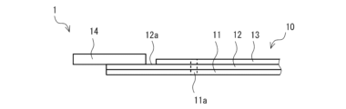
- FIG. 2 is a schematic side view of the flexible printed wiring board of FIG. 1.
- FIG. 3 is a schematic flow diagram showing a method for manufacturing a flexible printed wiring board according to one aspect of the present disclosure.
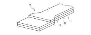
- FIG. 4 is a schematic perspective view of the laminate.
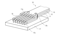
- FIG. 5 is a schematic perspective view showing a state in which the comb teeth and position fixing holes are formed by the comb teeth forming mold in the comb teeth forming step.
- FIG. 6 is a schematic plan view showing a state in which the wiring board main body is placed on a transport board.
- FIG. 7 is a schematic side view showing the state of FIG. 6.
- FIG. 8 is a schematic side view showing a state in which the connection terminal is fixed to the component fixing jig in the connection terminal fixing process.
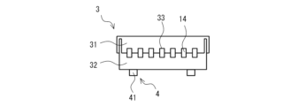
- FIG. 9 is a schematic bottom view showing the component fixing jig of FIG. 8.
- FIG. 10 is a schematic front view showing the component fixing jig shown in FIG. 8.
- FIG. 11 is a schematic front view showing a state in which the connection terminal is being fixed to the component fixing jig shown in FIG. 8.
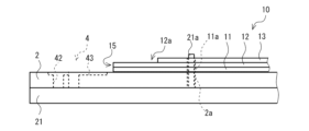
- FIG. 12 is a schematic side view showing a state in which the component fixing jig and the wiring board main body are placed on the transport board.
- FIG. 13 is a schematic side view showing a state in which a component fixing jig and a wiring board main body according to an embodiment different from FIG. 12 are placed on a transport board.
- connection terminals have a vertically elongated shape and are mounted side by side at a narrow pitch, so that the pitch between the connection terminals will not be constant due to slight mounting deviation. Therefore, it is required to mount with high precision, and it is necessary to perform positioning with high precision using, for example, a machine. In addition, productivity is low because the components are mounted one by one.
- the present disclosure has been made based on the above-mentioned circumstances, and an object of the present disclosure is to provide a method for manufacturing a flexible printed wiring board in which connection terminals can be easily mounted and productivity is high.
- the flexible printed wiring board manufacturing method of the present disclosure allows connection terminals to be easily mounted and has high productivity.
- a method for manufacturing a flexible printed wiring board includes a wiring board main body having an insulating base film and a conductive pattern laminated on one surface of the base film, and a wiring board main body having a conductive pattern laminated on one surface of the base film;
- a method for manufacturing a flexible printed wiring board comprising a plurality of connection terminals fixed to a terminal connection area provided at one end edge of a pattern, the method comprising: placing the wiring board main body on a transport board; and a component fixing tool.
- the plurality of connection terminals fixed in the fixing step are fixed in the terminal connection area of the wiring board body placed in the step of fixing the plurality of connection terminals in parallel to the fixture, and the step of placing the plurality of connection terminals in the fixing step.
- a positioning mechanism is provided between the transport board and the component fixing jig, and the positioning mechanism is used to mount the component fixing jig in the mounting process. Mount it on the above transport board.
- connection terminals are fixed in parallel to a component fixing jig and mounted at once. Further, direction deviation is less likely to occur between the connection terminals.
- a positioning mechanism between a transport board that supports the wiring board body and the component fixing jig positions the component fixing jig with respect to the carrier board for mounting. do.
- the positioning between the flexible printed wiring board and the transport board is performed by a mounting machine, but if the flexible printed wiring board manufacturing method is followed, it is also possible to perform the mounting manually, for example. That is, by using the flexible printed wiring board manufacturing method, connection terminals can be easily mounted.
- the positioning mechanism includes a columnar part provided on the component fixing jig, and a positioning hole provided on the transport board and capable of fitting into the columnar part.
- the wiring board body is provided with a wiring board body fixing hole into which the columnar part can fit, and in the mounting process, the wiring board body fixing hole is used to connect the wiring board body and the component fixing jig. It is advisable to perform positioning between the two. By providing the holes for fixing the wiring board body in this manner, it is possible to position the transport board, the wiring board body, and the component fixing jig at once via the columnar portion, thereby increasing the mounting accuracy of the connection terminals.
- the positioning mechanism has a plurality of pairs of the columnar portion and the positioning hole. As described above, since the positioning mechanism has a plurality of pairs of the columnar portion and the positioning hole, the component fixing jig can be positioned more reliably.
- the plurality of columnar parts are provided asymmetrically with respect to the geometric center of gravity position in the plan view shape of the component fixing jig.
- the "geometric center of gravity position in the planar view shape of the component fixing jig" refers to the gravity center position determined only from the planar view shape of the component fixing jig, and does not take into account differences in the density of each part. For example, when the component fixing jig is rectangular in plan view, the geometric center of gravity is the intersection of two diagonals of this rectangle.
- laminated on one surface is a concept that includes not only direct lamination on one surface but also indirect lamination via another layer or the like.
- the flexible printed wiring board 1 includes a wiring board main body 10 and a plurality of connection terminals 14.
- the wiring board main body 10 has an insulating base film 11 and a conductive pattern 12 laminated on one surface of the base film 11. Further, the plurality of connection terminals 14 are fixed to a terminal connection region 12a provided at one end edge of the conductive pattern 12 of the wiring board main body 10.
- the base film 11 is a member that supports the conductive pattern 12 and is a structural material that ensures the strength of the flexible printed wiring board 1.
- the main components of the base film 11 include, for example, polyimide, liquid crystal polymers such as liquid crystal polyester, soft materials such as polyethylene terephthalate, polyethylene naphthalate, polyphenylene ether, fluorine resin, paper phenol, paper epoxy, glass composite, and glass epoxy. , a hard material such as a glass base material, a rigid flexible material that is a composite of a soft material and a hard material, etc. can be used. Among these, polyimide is preferred because of its excellent heat resistance.
- the base film 11 may be porous, and may also contain fillers, additives, and the like.
- the "main component" refers to the component that is contained in the largest amount, and the content thereof is 50% by mass or more.
- the thickness of the base film 11 is not particularly limited, but the lower limit of the average thickness of the base film 11 is preferably 5 ⁇ m, more preferably 12 ⁇ m. Further, the upper limit of the average thickness of the base film 11 is preferably 500 ⁇ m, more preferably 200 ⁇ m. If the average thickness of the base film 11 is less than the above lower limit, the strength of the base film 11 may be insufficient. On the other hand, if the average thickness of the base film 11 exceeds the above upper limit, the flexibility of the flexible printed wiring board 1 may become insufficient.
- the "average thickness” refers to the average value of thicknesses measured at ten arbitrary points.
- the base film 11 has one or more position fixing holes 11a.
- the position fixing hole 11a is provided to penetrate the coverlay 13. Further, the position fixing hole 11a is provided to penetrate the conductive pattern 12 when it overlaps the conductive pattern 12 in a plan view.
- a positioning pin 21a is inserted into the position fixing hole 11a, and the wiring board main body 10 is fixed in position (see FIGS. 6 and 7).
- the shape of the position fixing hole 11a in plan view is not particularly limited, and may be polygonal, for example, but preferably circular as shown in FIG.
- the position fixing hole 11a has a circular shape in plan view, it is easy to insert the hole 11a when used for positioning on the transport board 2, and it is possible to prevent the strength of the base film 11 from decreasing.
- the number of position fixing holes 11a is preferably 2 or more and 5 or less, and more preferably 2 or 3. If the number of position fixing holes 11a is less than the above-mentioned lower limit, that is, 1, the wiring board body 10 fixed to the transport board 2 is likely to rotate around the position fixing holes 11a, and there is a possibility that the position cannot be fixed sufficiently. . On the other hand, if the number of positioning holes 11a exceeds the above upper limit, the number of positioning pins 21a to be inserted when positioning the wiring board body 10 on the transport board 2 increases unnecessarily, and work efficiency decreases. There is a risk.
- This position fixing hole 11a is provided at a position that does not affect the circuit pattern configured on the flexible printed wiring board 1, but it is preferably provided within or near the terminal connection area 12a. By providing the position fixing hole 11a in or near the terminal connection area 12a, the position fixing hole 11a is located at one end edge of the conductive pattern 12 relatively close to the connection terminal 14, so that it can be positioned relative to the component fixing jig 3 described later. Easy to prevent misalignment.
- the lower limit of the distance from the one end edge of the position fixing hole 11a (the distance between the center of the position fixing hole 11a and the one end edge) is preferably 4 mm, more preferably 5 mm.
- the upper limit of the distance from the one end edge of the position fixing hole 11a is preferably 50 mm, more preferably 40 mm. If the distance from the one end edge of the position fixing hole 11a is less than the lower limit, the position fixing hole 11a may interfere with the connection terminal 14. On the other hand, if the distance from the one end edge of the position fixing hole 11a exceeds the above upper limit, there is a possibility that relative positional deviation with the component fixing jig 3 will easily occur.
- the lower limit of the diameter of the position fixing hole 11a (the diagonal length if the position fixing hole 11a is polygonal) in plan view is preferably 0.5 mm, more preferably 1 mm.
- the upper limit of the diameter of the position fixing hole 11a is preferably 5 mm, more preferably 4 mm. If the diameter of the position fixing hole 11a is less than the above lower limit, the positioning pin 21a becomes too thin and may be easily damaged. Conversely, if the diameter of the position fixing hole 11a exceeds the above upper limit, the strength of the base film 11 may be reduced due to the position fixing hole 11a.
- the lower limit of the distance (minimum distance) between the centers of adjacent position fixing holes 11a is preferably 1 mm, and more preferably 2 mm. If the distance between the centers of the position fixing holes 11a is less than the above-mentioned lower limit, the effect of improving the alignment accuracy may be insufficient.
- the upper limit of the distance between the centers of the position fixing holes 11a is not particularly limited, but is determined by, for example, the width of the base film 11.
- the conductive pattern 12 constitutes a structure such as an electric wiring structure, a ground, and a shield.
- the material forming the conductive pattern 12 is not particularly limited as long as it has conductivity, but examples include metals such as copper, aluminum, and nickel. Generally, copper is relatively inexpensive and has high conductivity. used. Further, the surface of the conductive pattern 12 may be subjected to plating treatment.
- the lower limit of the average thickness of the conductive pattern 12 is preferably 2 ⁇ m, more preferably 5 ⁇ m.
- the upper limit of the average thickness of the conductive pattern 12 is preferably 100 ⁇ m, more preferably 70 ⁇ m.
- the conductivity of the conductive pattern 12 may be insufficient.
- flexible printed wiring board 1 may become unnecessarily thick.
- a terminal connection area 12a that the flexible printed wiring board 1 has at one end edge of the conductive pattern 12 is an area for connecting to other electronic equipment etc. via a connection terminal 14, which will be described later.
- a coverlay 13 which will be described later, is removed.
- the terminal connection area 12a is located at the periphery of the flexible printed wiring board 1 (for example, in the case of a rectangular flexible printed wiring board 1, one short side thereof) in order to connect to other electronic devices, etc.
- the terminal end (one edge) of the conductive pattern 12 is configured to be connected to the connection terminal 14 provided in the terminal connection area 12a.
- the shape of the terminal connection region 12a is a comb-teeth shape in which the one end edge is branched, as shown in FIG.
- One connection terminal 14 is provided for each comb tooth portion 15 of the comb teeth.
- the size of the comb teeth portion 15 is appropriately determined depending on the size of the connection terminal 14, and may be, for example, an average width of 0.5 mm or more and 3 mm or less, and an average length of 3 mm or more and 50 mm or less. Further, the number of comb teeth portions 15 is determined in accordance with the number of connection terminals 14. Normally, the width of the base film 11 including the terminal connection area 12a is constant, but depending on the number of connection terminals 14, the width may not fit within the width of the base film 11 excluding the terminal connection area 12a. In such a case, the number of comb teeth portions 15 can be secured by widening the width of the base film 11 at one end, as shown in FIG. 1, for example.
- the coverlay 13 protects the conductive pattern 12 from external force, moisture, and the like.
- Coverlay 13 has a cover film and an adhesive layer.
- the coverlay 13 is obtained by laminating a cover film on the surface of the conductive pattern 12 opposite to the base film 11 via this adhesive layer.
- the material of the cover film is not particularly limited, but for example, the same material as the resin constituting the base film 11 can be used.
- the lower limit of the average thickness of the cover film is preferably 5 ⁇ m, more preferably 10 ⁇ m.
- the upper limit of the average thickness of the cover film is preferably 50 ⁇ m, more preferably 30 ⁇ m. If the average thickness of the cover film is less than the lower limit, the insulation may be insufficient. Conversely, if the average thickness of the cover film exceeds the upper limit, the flexibility of the flexible printed wiring board 1 may be impaired.
- the adhesive layer fixes the cover film to the conductive pattern 12 and the base film 11.
- the material of the adhesive layer is not particularly limited as long as it can fix the cover film to the conductive pattern 12 and the base film 11, but materials with excellent flexibility and heat resistance are preferable, such as polyimide, polyamide, epoxy, etc. , butyral, acrylic, etc. Furthermore, thermosetting resins are preferred in terms of heat resistance.
- the average thickness of the adhesive layer is not particularly limited, but the lower limit of the average thickness of the adhesive layer is, for example, preferably 5 ⁇ m, more preferably 10 ⁇ m.
- the upper limit of the average thickness of the adhesive layer is preferably, for example, 100 ⁇ m, more preferably 80 ⁇ m. If the average thickness of the adhesive layer is less than the lower limit, the adhesiveness may be insufficient. Conversely, if the average thickness of the adhesive layer exceeds the upper limit, the flexibility of the flexible printed wiring board 1 may be impaired.
- connection terminal 14 is a component for connecting the flexible printed wiring board 1 to other electronic equipment or the like.
- the material of the connecting terminal 14 is not particularly limited as long as it has conductivity, but for example, the connecting terminal 14 can be made of metal.
- the metal include annealed copper, brass, and phosphor bronze.
- the surface of the connection terminal 14 is preferably plated to prevent oxidation. Examples of the above-mentioned plating include Sn plating, Ni plating, and Au plating. Among these, Ni plating is preferred because it is inexpensive and has excellent corrosion resistance.
- connection terminal 14 is appropriately determined depending on the terminal shape of the electronic device to be connected, etc., but is generally vertically long (long in the length direction of the base film 11).
- the shape of the connecting terminal 14 may be, for example, a plate shape or a molded three-dimensional shape with an average width of 0.5 mm or more and 3 mm or less, an average length of 3 mm or more and 50 mm or less, and an average height of 0.1 mm or more and 3 mm or less.
- connection terminal 14 protrudes from the one end edge.
- the average length of this protruding portion is preferably 20% or more and 80% or less of the average length of the connecting terminal 14, although it depends on the terminal shape of the electronic device etc. to be connected. If the average length of the protruding portions is less than the lower limit, the adhesive strength to other electronic devices or the like may be insufficient. Conversely, if the average length of the protruding portion exceeds the upper limit, the adhesive strength to the flexible printed wiring board 1 may be insufficient.
- the method for manufacturing the flexible printed wiring board includes a laminate forming step S1, a comb tooth forming step S2, a wiring board body mounting step S3, a connecting terminal fixing step S4, and a connecting terminal mounting step.
- the process includes step S5 and jig removal step S6.
- a base film 11 having an insulating property, a conductive pattern 12 laminated on one side of the base film 11, and a cover layer laminated on one side of the base film 11 or the conductive pattern 12 are formed. 13 (see FIG. 4). Specifically, the procedure is as follows.
- a conductor layer is formed on one side of the base film 11.
- the conductor layer can be formed, for example, by bonding a foil conductor using an adhesive or by a known film forming method.
- the above-mentioned conductor is made of the same material as the material constituting the conductive pattern 12, and examples thereof include copper, silver, gold, nickel, and the like.
- the adhesive is not particularly limited as long as it can bond the conductor to the base film 11, and various known adhesives can be used. Examples of the film forming method include vapor deposition, plating, and the like.
- the conductor layer is preferably formed by bonding copper foil to the base film 11 using a polyimide adhesive.
- this conductor layer is patterned to form a conductive pattern 12.
- Patterning of the conductor layer can be performed by a known method, for example, photoetching.
- Photo-etching is performed by forming a resist film having a predetermined pattern on one surface of the conductor layer, and then treating the conductor layer exposed from the resist film with an etching solution to remove the resist film.
- the coverlay 13 is laminated to cover the conductive pattern 12 except for the terminal connection area 12a at one end edge of the conductive pattern 12.
- an adhesive layer is laminated on the surface of the base film 11 on which the conductive pattern 12 is formed, and a cover film is laminated on the adhesive layer.
- an adhesive layer may be laminated on the cover film in advance, and the surface of the cover film on which the adhesive layer is laminated may be made to face the conductive pattern 12 and bonded.
- Adhesion of the cover film using an adhesive can usually be performed by thermocompression bonding.
- the temperature and pressure during thermocompression bonding may be appropriately determined depending on the type and composition of the adhesive used.
- the laminate 16 can be formed.
- the comb tooth portion 15 is formed at one end edge of the conductive pattern 12 of the laminate 16 formed in the laminate forming step S1.
- the patterning shape of the conductive pattern 1 in the portion where the comb teeth portions 15 are formed is not particularly limited, but may be, for example, a patterning shape in which each of the comb teeth portions 15 is connected to an individual pattern. can do.
- the comb tooth portion 15 can be formed by punching using a die (comb tooth portion forming mold 17) that punches out the gap between the comb tooth portions 15, as shown in FIG.
- the comb tooth portion forming mold 17 includes a cutting die 17a corresponding to the gap between the comb teeth portions 15 and a cutting die 17b corresponding to the position fixing hole 11a.
- the position fixing hole 11a can be formed using the mold for forming the comb tooth portion 15.
- the material of this comb-teeth forming mold 17 is not particularly limited, and may be, for example, general carbon tool steel (SK material). Further, the shape of the comb tooth portion forming mold 17 is appropriately determined to be a shape that allows processing of the comb tooth portion 15 and the position fixing hole 11a.
- SK material general carbon tool steel
- the wiring board main body 10 is formed in the above manner.
- the transport board 2 is a board used when manufacturing the flexible printed wiring board 1.
- the conveyance board 2 has a certain strength and is made of, for example, a metal plate such as SUS, aluminum, or titanium, a resin plate such as glass epoxy, or a laminated plate of glass cloth.
- the size of the transport board 2 in plan view is such that it can mount the wiring board main body 10 and the component fixing jig 3 described below, and its shape can be, for example, rectangular.
- a positioning board 21 is used to align the transport board 2 and the wiring board body 10.
- the positioning board 21 shown in FIGS. 6 and 7 has the same shape as the transport board 2 in plan view, but the positioning board 21 may be larger than the transport board 2, and a plurality of transport boards 2 can be combined into one positioning board 21. It may be configured so that it can be placed on.
- the positioning board 21 is provided with columnar positioning pins 21a for fixing the wiring board main body 10. Furthermore, the transport board 2 is provided with a through hole 2a that is continuous with the position fixing hole 11a when the wiring board main body 10 is placed thereon.
- the wiring board main body 10 can be fixed to the transport board 2 by fitting the transport board 2 into the positioning pin 21a (by passing the positioning pin 21a through the through hole 2a) and further fitting into the position fixing hole 11a of the wiring board main body 10. It is configured as follows. Specifically, it is preferable that the position fixing hole 11a and the through hole 2a have the same diameter (having the same shape in cross section). Further, the length of the positioning pin 21a is at least longer than the length of the through hole 2a, and preferably longer than the sum of the length of the position fixing hole 11a and the length of the through hole 2a.
- the cross section of the positioning pin 21a is preferably the same as the position fixing hole 11a and the through hole 2a, and has a size that allows the position fixing hole 11a and the through hole 2a to pass through.
- the wiring board body 10 is placed on the transport board 2 so that the position fixing hole 11a and the through hole 2a overlap in plan view, It is fixed with the positioning pin 21a.
- connection terminal fixing step S4 does not matter. It is also possible to perform the wiring board body mounting step S3 after the connection terminal fixing step S4.
- connection terminal fixing step S4 As shown in FIGS. 8, 9, and 10, a plurality of connection terminals 14 are fixed in parallel to the component fixing jig 3.
- the component fixing jig 3 used in the connection terminal fixing step S4 has an upper jig 31 that constitutes the upper part of the component fixing jig 3, and an upper jig 31 that fits into the upper jig 31, as shown in FIGS. 8, 9, and 10, for example. It has a lower jig 32 that can be assembled together, and a holding hole 33 that can hold the connecting terminal 14.
- the component fixing jig 3 has a rectangular parallelepiped shape as a whole.
- the material of the component fixing jig 3 is not particularly limited, and may be, for example, general carbon tool steel (SK material).
- the recess provided on the bottom surface of the upper jig 31 and the recess provided on the top surface of the lower jig 32 are combined in the vertical direction, and the holding hole 33 is opened. configured.
- the number of holding holes 33 is the same as the number of connection terminals 14 of the flexible printed wiring board 1 to be manufactured, and the spacing between adjacent holding holes 33 is also the same as the spacing between adjacent connection terminals 14.
- the depth of the holding hole 33 of the component fixing jig 3 is determined in accordance with the average length of the protruding portion of the connection terminal 14 after mounting.
- the plurality of connection terminals 14 can be fixed in parallel as follows. That is, first, the connection terminals 14 are fitted into the respective recesses of the lower jig 32. Next, the upper jig 31 is fitted into the lower jig 32 from above (see FIG. 11). At this time, the recess provided in the upper jig 31 is combined with the recess provided in the lower jig 32, and the connection terminal 14 can be fixed in the holding hole 33.
- connection terminal mounting step S5 the terminals fixed in the fixing step (connection terminal fixing step S4) are placed on the terminal connection area 12a of the wiring board body 10 placed in the mounting step (wiring board body mounting step S3).
- a plurality of connection terminals 14 are mounted together with the component fixing jig 3.
- the component fixing jig 3 is mounted on the transportation board 2 using the positioning mechanism 4 provided between the transportation board 2 and the component fixing jig 3.
- the positioning mechanism 4 will be explained below.
- the positioning mechanism 4 includes a columnar part 41 provided on the component fixing jig 3 shown in FIGS. 8, 9, and 10, and a columnar part 41 provided on the transport board 2 as shown in FIG. It includes a positioning hole 42. By configuring the positioning mechanism 4 as described above, the component fixing jig 3 can be easily mounted on the transport board 2.
- the positioning mechanism 4 preferably has a plurality of pairs of columnar parts 41 and positioning holes 42. Since the positioning mechanism 4 has a plurality of pairs of columnar parts 41 and positioning holes 42 in this way, the component fixing jig 3 can be positioned more reliably.
- the positioning mechanism 4 shown in FIGS. 8, 9, and 10 has two pairs of columnar parts 41 and positioning holes 42. As shown in FIG. The following explanation will be continued taking as an example a case where two pairs of columnar parts 41 and positioning holes 42 are provided, but the number of columnar parts 41 and positioning holes 42 is not limited to two pairs, and is one pair or three pairs. It may be more than that.
- the plurality of columnar parts 41 are provided asymmetrically with respect to the geometric center of gravity G in the plan view shape of the component fixing jig 3. In this way, by providing the columnar portions 41 asymmetrically with respect to the geometric center of gravity position G in the plan view of the component fixing jig 3, incorrect mounting can be easily avoided. In other words, if you attempt to mount the component fixing jig 3 with its front and back or left and right sides reversed, some of the plurality of pairs of columnar parts 41 and positioning holes 42 will not match or will be mounted in significantly different positions. Workers can easily understand that the implementation is incorrect.
- the planar shape of the columnar portion 41 can be circular as shown in FIG.
- the shape in plan view is circular, it is easy to insert the component fixing jig 3 when used for alignment to the transport board 2.
- the shape of the columnar portion 41 in plan view may be a polygonal shape such as a triangular shape. In this case, since the direction in which it can be inserted is limited, incorrect mounting can be avoided even if there is only one pair of columnar portions 41 and positioning holes 42.
- the shape of the positioning hole 42 in plan view is the same as the shape of the columnar part 41 in plan view. Further, the positioning hole 42 may penetrate through the conveyance board 2 as shown in FIG. 7, but it may also be a recessed portion deeper than the length of the columnar portion 41.
- the positioning mechanism 4 may be provided on the transport board 2 and may have a bottom fitting part 43 that can fit with the bottom of the component fixing jig 3.
- the bottom fitting portion 43 can also be used as an adjustment allowance for adjusting the height of the connection terminal 14 fixed to the component fixing jig 3 to the height of the terminal connection area 12a of the wiring board main body 10.
- connection terminal mounting step S5 when the component fixing jig 3 is mounted on the transport board 2 so that its bottom part fits into the bottom fitting part 43, the columnar part 41 is inevitably guided to the corresponding positioning hole 42. and inserted. In this way, the component fixing jig 3 can be mounted on the transport board 2. At this time, the component fixing jig 3 is fixed so as not to move on the transfer board 2 mainly by the columnar part 41 and the positioning hole 42, and the plurality of connection terminals 14 are placed at the mounting position of the corresponding comb tooth part 15. be done.
- connection terminals 14 are soldered to the conductive patterns 12.
- the positioning board 21 is usually removed after placing the plurality of connection terminals 14 at the mounting positions of the corresponding comb teeth portions 15 and before reflowing.
- connection terminals 14 are mounted and the flexible printed wiring board 1 is formed.
- the plurality of connection terminals 14 are fixed in parallel to the component fixing jig 3 and mounted at once, so productivity is high. Further, direction deviation is less likely to occur between the connection terminals 14. Furthermore, in the flexible printed wiring board manufacturing method, the positioning mechanism 4 between the transport board 2 that supports the wiring board body 10 and the component fixing jig 3 positions the component fixing jig 3 with respect to the transport board 2. and implement it. For this reason, there is no need to use a machine to perform accurate positioning as in the case of positioning with the flexible wiring board main body 10, and it is also possible to mount the board manually, for example. That is, by using the flexible printed wiring board manufacturing method, the connection terminals 14 can be easily mounted.
- the positioning mechanism is composed of a columnar part provided on a component fixing jig and a positioning hole provided on a transport board and capable of fitting with the columnar part.
- Other configurations may also be adopted as long as they are provided between the transport board and the component fixing jig.
- a columnar portion may be provided on the transport board, and positioning holes may be provided on the component fixing jig.
- it may be configured with only a bottom fitting portion that can fit with the bottom of the above-mentioned component fixing jig.
- the wiring board body 10 is provided with a wiring board body fixing hole 11b into which the columnar part 44 of the positioning mechanism 4 can fit, and the connection terminal mounting process (mounting process) It is also possible to adopt a configuration in which positioning between the wiring board main body 10 and the component fixing jig 3 is performed using the wiring board main body fixing hole 11b.
- the wiring board main body fixing hole 11b also serves as a positioning hole for the transport board and the component fixing jig.
- the method for manufacturing the flexible printed wiring board includes a laminate forming step, but the laminate forming step is not an essential component.
- the method for manufacturing a flexible printed wiring board can also be used for a laminate prepared in advance.
- the method for manufacturing the flexible printed wiring board includes a comb tooth portion forming step, but the comb tooth portion forming step is not an essential component.
- the method for manufacturing a flexible printed wiring board can also be used for a flexible printed wiring board that does not have a comb tooth portion and has, for example, a rectangular terminal connection area in plan view.
- the method for manufacturing the flexible printed wiring board includes a jig removal process, but the jig removal process is not an essential component.
- the component fixing jig is used as it is as a part of a flexible printed wiring board, such as a housing for a connection terminal, there is no need to remove the jig, and the jig removal process can be omitted.
- the position fixing hole is formed using a mold for forming the comb tooth part, but different molds are used for the comb tooth part and the position fixing hole. They may also be formed separately. Even when the comb tooth portion and the position fixing hole are formed separately, the connection terminal can be easily mounted by using the flexible printed wiring board manufacturing method.
- a case has been described in which a plurality of connection terminals are mounted at once using a component fixing jig, but as long as a plurality of connection terminals are mounted at one time, it may be mounted in parts.
- Divided mounting reduces the number of connection terminals that must be fixed at once, allowing the component fixing jig to be made smaller.
- the upper limit of the number of divisions in the case of divisional mounting is preferably 4, more preferably 3, and even more preferably 2. If the number of divisions exceeds the above upper limit, there is a risk that mounting accuracy will decrease and productivity may decrease.
- the shape of the component fixing jig is not limited to the above embodiment.
- the part for fixing the connection terminal may be a recess provided in the lower jig of the component fixing jig, and the upper jig may not be provided.
- the flexible printed wiring board is not limited to the above-mentioned embodiments, and the flexible printed wiring board may also be used, such as a flexible printed wiring board that has a reinforcing portion on the other side of the base film, or a flexible printed wiring board that does not have a coverlay.
- a method of manufacturing a plate can be used.
Landscapes
- Engineering & Computer Science (AREA)
- Microelectronics & Electronic Packaging (AREA)
- Manufacturing & Machinery (AREA)
- Electric Connection Of Electric Components To Printed Circuits (AREA)
Priority Applications (2)
| Application Number | Priority Date | Filing Date | Title |
|---|---|---|---|
| JP2024535047A JPWO2024018969A1 (https=) | 2022-07-20 | 2023-07-12 | |
| CN202380048948.1A CN119422295A (zh) | 2022-07-20 | 2023-07-12 | 柔性印刷布线板的制造方法 |
Applications Claiming Priority (2)
| Application Number | Priority Date | Filing Date | Title |
|---|---|---|---|
| JP2022115864 | 2022-07-20 | ||
| JP2022-115864 | 2022-07-20 |
Publications (1)
| Publication Number | Publication Date |
|---|---|
| WO2024018969A1 true WO2024018969A1 (ja) | 2024-01-25 |
Family
ID=89617853
Family Applications (1)
| Application Number | Title | Priority Date | Filing Date |
|---|---|---|---|
| PCT/JP2023/025777 Ceased WO2024018969A1 (ja) | 2022-07-20 | 2023-07-12 | フレキシブルプリント配線板の製造方法 |
Country Status (3)
| Country | Link |
|---|---|
| JP (1) | JPWO2024018969A1 (https=) |
| CN (1) | CN119422295A (https=) |
| WO (1) | WO2024018969A1 (https=) |
Citations (3)
| Publication number | Priority date | Publication date | Assignee | Title |
|---|---|---|---|---|
| JP2002299000A (ja) * | 2001-03-30 | 2002-10-11 | Fujikura Ltd | 可撓性プリント基板と接続端子の接合方法 |
| JP2011113676A (ja) * | 2009-11-24 | 2011-06-09 | Yazaki Corp | フレキシブルフラットケーブルに対する端子の接続方法および端子 |
| WO2019035334A1 (ja) * | 2017-08-14 | 2019-02-21 | 住友電工プリントサーキット株式会社 | フレキシブルプリント配線板の製造方法 |
-
2023
- 2023-07-12 JP JP2024535047A patent/JPWO2024018969A1/ja active Pending
- 2023-07-12 WO PCT/JP2023/025777 patent/WO2024018969A1/ja not_active Ceased
- 2023-07-12 CN CN202380048948.1A patent/CN119422295A/zh active Pending
Patent Citations (3)
| Publication number | Priority date | Publication date | Assignee | Title |
|---|---|---|---|---|
| JP2002299000A (ja) * | 2001-03-30 | 2002-10-11 | Fujikura Ltd | 可撓性プリント基板と接続端子の接合方法 |
| JP2011113676A (ja) * | 2009-11-24 | 2011-06-09 | Yazaki Corp | フレキシブルフラットケーブルに対する端子の接続方法および端子 |
| WO2019035334A1 (ja) * | 2017-08-14 | 2019-02-21 | 住友電工プリントサーキット株式会社 | フレキシブルプリント配線板の製造方法 |
Also Published As
| Publication number | Publication date |
|---|---|
| CN119422295A (zh) | 2025-02-11 |
| JPWO2024018969A1 (https=) | 2024-01-25 |
Similar Documents
| Publication | Publication Date | Title |
|---|---|---|
| US10796837B2 (en) | Electronic component, diaphragm, and electronic device | |
| CN105228341B (zh) | 印刷电路板、封装基板及其制造方法 | |
| EP2624673B1 (en) | Substrate with built-in component and method for manufacturing substrate with built-in component | |
| JP5441007B2 (ja) | 電子部品内蔵基板の製造方法 | |
| JP3840180B2 (ja) | フレキシブルプリント配線板 | |
| CN107770947A (zh) | 印刷布线板和印刷布线板的制造方法 | |
| US11483928B2 (en) | Flexible printed circuit board | |
| CN110856375B (zh) | 热压熔锡焊接电路板及其制作方法 | |
| WO2019035248A1 (ja) | フレキシブルプリント配線板 | |
| US11051399B2 (en) | Flexible printed circuit board | |
| US8479385B2 (en) | Method of producing wiring substrate | |
| CN213124101U (zh) | 多层基板以及多层基板的安装构造 | |
| CN101499453B (zh) | 配线电路基板及其制造方法 | |
| JP2009231635A (ja) | 配線基板及びその製造方法、及び半導体装置及びその製造方法 | |
| WO2024018969A1 (ja) | フレキシブルプリント配線板の製造方法 | |
| JP6959342B2 (ja) | フレキシブルプリント配線板の製造方法 | |
| JP2019021863A (ja) | 多層基板 | |
| CN109950017B (zh) | 电子部件以及电子部件的制造方法 | |
| CN110972413B (zh) | 复合电路板及其制作方法 | |
| WO2011043382A1 (ja) | 回路基板及びその製造方法 | |
| JP5579559B2 (ja) | フレキシブルプリント配線板の接続構造 | |
| KR101189330B1 (ko) | 인쇄회로기판 및 그의 제조 방법 | |
| JP6735793B2 (ja) | 複合基板及びリジッド基板 | |
| US20200120797A1 (en) | Flipped-Conductor-Patch Lamination for Ultra Fine-Line Substrate Creation | |
| JP2008147228A (ja) | 配線基板及びその製造方法 |
Legal Events
| Date | Code | Title | Description |
|---|---|---|---|
| 121 | Ep: the epo has been informed by wipo that ep was designated in this application |
Ref document number: 23842892 Country of ref document: EP Kind code of ref document: A1 |
|
| WWE | Wipo information: entry into national phase |
Ref document number: 2024535047 Country of ref document: JP |
|
| WWE | Wipo information: entry into national phase |
Ref document number: 202380048948.1 Country of ref document: CN |
|
| WWP | Wipo information: published in national office |
Ref document number: 202380048948.1 Country of ref document: CN |
|
| NENP | Non-entry into the national phase |
Ref country code: DE |
|
| 122 | Ep: pct application non-entry in european phase |
Ref document number: 23842892 Country of ref document: EP Kind code of ref document: A1 |