WO2024014223A1 - 基板保持装置、基板製造装置、および基板製造方法 - Google Patents
基板保持装置、基板製造装置、および基板製造方法 Download PDFInfo
- Publication number
- WO2024014223A1 WO2024014223A1 PCT/JP2023/022255 JP2023022255W WO2024014223A1 WO 2024014223 A1 WO2024014223 A1 WO 2024014223A1 JP 2023022255 W JP2023022255 W JP 2023022255W WO 2024014223 A1 WO2024014223 A1 WO 2024014223A1
- Authority
- WO
- WIPO (PCT)
- Prior art keywords
- substrate
- holding
- fluid
- holding roller
- roller
- Prior art date
- Legal status (The legal status is an assumption and is not a legal conclusion. Google has not performed a legal analysis and makes no representation as to the accuracy of the status listed.)
- Ceased
Links
Images


Classifications
-
- H—ELECTRICITY
- H01—ELECTRIC ELEMENTS
- H01L—SEMICONDUCTOR DEVICES NOT COVERED BY CLASS H10
- H01L21/00—Processes or apparatus adapted for the manufacture or treatment of semiconductor or solid state devices or of parts thereof
- H01L21/67—Apparatus specially adapted for handling semiconductor or electric solid state devices during manufacture or treatment thereof; Apparatus specially adapted for handling wafers during manufacture or treatment of semiconductor or electric solid state devices or components ; Apparatus not specifically provided for elsewhere
- H01L21/683—Apparatus specially adapted for handling semiconductor or electric solid state devices during manufacture or treatment thereof; Apparatus specially adapted for handling wafers during manufacture or treatment of semiconductor or electric solid state devices or components ; Apparatus not specifically provided for elsewhere for supporting or gripping
-
- H—ELECTRICITY
- H01—ELECTRIC ELEMENTS
- H01L—SEMICONDUCTOR DEVICES NOT COVERED BY CLASS H10
- H01L21/00—Processes or apparatus adapted for the manufacture or treatment of semiconductor or solid state devices or of parts thereof
- H01L21/02—Manufacture or treatment of semiconductor devices or of parts thereof
- H01L21/04—Manufacture or treatment of semiconductor devices or of parts thereof the devices having potential barriers, e.g. a PN junction, depletion layer or carrier concentration layer
- H01L21/18—Manufacture or treatment of semiconductor devices or of parts thereof the devices having potential barriers, e.g. a PN junction, depletion layer or carrier concentration layer the devices having semiconductor bodies comprising elements of Group IV of the Periodic Table or AIIIBV compounds with or without impurities, e.g. doping materials
- H01L21/30—Treatment of semiconductor bodies using processes or apparatus not provided for in groups H01L21/20 - H01L21/26
- H01L21/302—Treatment of semiconductor bodies using processes or apparatus not provided for in groups H01L21/20 - H01L21/26 to change their surface-physical characteristics or shape, e.g. etching, polishing, cutting
- H01L21/304—Mechanical treatment, e.g. grinding, polishing, cutting
-
- H—ELECTRICITY
- H01—ELECTRIC ELEMENTS
- H01L—SEMICONDUCTOR DEVICES NOT COVERED BY CLASS H10
- H01L21/00—Processes or apparatus adapted for the manufacture or treatment of semiconductor or solid state devices or of parts thereof
- H01L21/67—Apparatus specially adapted for handling semiconductor or electric solid state devices during manufacture or treatment thereof; Apparatus specially adapted for handling wafers during manufacture or treatment of semiconductor or electric solid state devices or components ; Apparatus not specifically provided for elsewhere
- H01L21/67005—Apparatus not specifically provided for elsewhere
- H01L21/67011—Apparatus for manufacture or treatment
- H01L21/67017—Apparatus for fluid treatment
- H01L21/67028—Apparatus for fluid treatment for cleaning followed by drying, rinsing, stripping, blasting or the like
- H01L21/6704—Apparatus for fluid treatment for cleaning followed by drying, rinsing, stripping, blasting or the like for wet cleaning or washing
- H01L21/67051—Apparatus for fluid treatment for cleaning followed by drying, rinsing, stripping, blasting or the like for wet cleaning or washing using mainly spraying means, e.g. nozzles
-
- H—ELECTRICITY
- H01—ELECTRIC ELEMENTS
- H01L—SEMICONDUCTOR DEVICES NOT COVERED BY CLASS H10
- H01L21/00—Processes or apparatus adapted for the manufacture or treatment of semiconductor or solid state devices or of parts thereof
- H01L21/67—Apparatus specially adapted for handling semiconductor or electric solid state devices during manufacture or treatment thereof; Apparatus specially adapted for handling wafers during manufacture or treatment of semiconductor or electric solid state devices or components ; Apparatus not specifically provided for elsewhere
- H01L21/67005—Apparatus not specifically provided for elsewhere
- H01L21/67011—Apparatus for manufacture or treatment
- H01L21/6715—Apparatus for applying a liquid, a resin, an ink or the like
-
- H—ELECTRICITY
- H01—ELECTRIC ELEMENTS
- H01L—SEMICONDUCTOR DEVICES NOT COVERED BY CLASS H10
- H01L21/00—Processes or apparatus adapted for the manufacture or treatment of semiconductor or solid state devices or of parts thereof
- H01L21/67—Apparatus specially adapted for handling semiconductor or electric solid state devices during manufacture or treatment thereof; Apparatus specially adapted for handling wafers during manufacture or treatment of semiconductor or electric solid state devices or components ; Apparatus not specifically provided for elsewhere
- H01L21/683—Apparatus specially adapted for handling semiconductor or electric solid state devices during manufacture or treatment thereof; Apparatus specially adapted for handling wafers during manufacture or treatment of semiconductor or electric solid state devices or components ; Apparatus not specifically provided for elsewhere for supporting or gripping
- H01L21/687—Apparatus specially adapted for handling semiconductor or electric solid state devices during manufacture or treatment thereof; Apparatus specially adapted for handling wafers during manufacture or treatment of semiconductor or electric solid state devices or components ; Apparatus not specifically provided for elsewhere for supporting or gripping using mechanical means, e.g. chucks, clamps or pinches
- H01L21/68714—Apparatus specially adapted for handling semiconductor or electric solid state devices during manufacture or treatment thereof; Apparatus specially adapted for handling wafers during manufacture or treatment of semiconductor or electric solid state devices or components ; Apparatus not specifically provided for elsewhere for supporting or gripping using mechanical means, e.g. chucks, clamps or pinches the wafers being placed on a susceptor, stage or support
- H01L21/68764—Apparatus specially adapted for handling semiconductor or electric solid state devices during manufacture or treatment thereof; Apparatus specially adapted for handling wafers during manufacture or treatment of semiconductor or electric solid state devices or components ; Apparatus not specifically provided for elsewhere for supporting or gripping using mechanical means, e.g. chucks, clamps or pinches the wafers being placed on a susceptor, stage or support characterised by a movable susceptor, stage or support, others than those only rotating on their own vertical axis, e.g. susceptors on a rotating caroussel
-
- H—ELECTRICITY
- H01—ELECTRIC ELEMENTS
- H01L—SEMICONDUCTOR DEVICES NOT COVERED BY CLASS H10
- H01L21/00—Processes or apparatus adapted for the manufacture or treatment of semiconductor or solid state devices or of parts thereof
- H01L21/67—Apparatus specially adapted for handling semiconductor or electric solid state devices during manufacture or treatment thereof; Apparatus specially adapted for handling wafers during manufacture or treatment of semiconductor or electric solid state devices or components ; Apparatus not specifically provided for elsewhere
- H01L21/683—Apparatus specially adapted for handling semiconductor or electric solid state devices during manufacture or treatment thereof; Apparatus specially adapted for handling wafers during manufacture or treatment of semiconductor or electric solid state devices or components ; Apparatus not specifically provided for elsewhere for supporting or gripping
- H01L21/687—Apparatus specially adapted for handling semiconductor or electric solid state devices during manufacture or treatment thereof; Apparatus specially adapted for handling wafers during manufacture or treatment of semiconductor or electric solid state devices or components ; Apparatus not specifically provided for elsewhere for supporting or gripping using mechanical means, e.g. chucks, clamps or pinches
- H01L21/68714—Apparatus specially adapted for handling semiconductor or electric solid state devices during manufacture or treatment thereof; Apparatus specially adapted for handling wafers during manufacture or treatment of semiconductor or electric solid state devices or components ; Apparatus not specifically provided for elsewhere for supporting or gripping using mechanical means, e.g. chucks, clamps or pinches the wafers being placed on a susceptor, stage or support
- H01L21/68785—Apparatus specially adapted for handling semiconductor or electric solid state devices during manufacture or treatment thereof; Apparatus specially adapted for handling wafers during manufacture or treatment of semiconductor or electric solid state devices or components ; Apparatus not specifically provided for elsewhere for supporting or gripping using mechanical means, e.g. chucks, clamps or pinches the wafers being placed on a susceptor, stage or support characterised by the mechanical construction of the susceptor, stage or support
Definitions
- the present invention relates to a substrate holding device, a substrate manufacturing device, and a substrate manufacturing method.
- the non-device surface of one substrate is ground.
- the substrate has a rounded shape or a chamfered shape (beveled portion) in advance at its peripheral edge.
- the bevel portion becomes thinner due to grinding, a sharp edge portion (knife edge portion) is formed, which may result in defects such as cracks and chips. Therefore, in the bevel fill technique, the gaps between the bevel parts in the laminated substrate are filled with a filler to support the knife edge part with the filler and prevent the occurrence of defects.
- an object of the present invention is to provide a substrate holding device, a substrate manufacturing device, and a substrate manufacturing method that can prevent defects from occurring in the substrate.
- a holding roller rotates the substrate while holding a beveled portion of the substrate; and a fluid blowing device connected to the holding roller and blowing pressurized fluid to the beveled portion held by the holding roller.
- a substrate holding device comprising:
- the fluid blowout device includes a fluid supply line connected to a blowout port formed in the holding roller, and a fluid supply device connected to the fluid supply line.
- the substrate holding device includes a clamping device that causes a first holding portion and a second holding portion of the holding roller that hold the bevel portion to approach or separate from each other.
- the substrate holding device includes a roller moving device that moves the holding roller between a contact position in which it contacts the bevel portion and a separation position in which it separates from the bevel portion.
- a substrate manufacturing apparatus that manufactures a laminated substrate formed by bonding a first substrate and a second substrate.
- the substrate manufacturing apparatus includes a holding roller that rotates the laminated substrate while holding the laminated substrate, and a fluid that is connected to the holding roller and blows pressurized fluid into a gap between the laminated substrate held by the holding roller.
- the device includes a blowing device and a coating device that applies a filler to the gap.
- the fluid blowout device includes a fluid supply line connected to a blowout port formed in the holding roller, and a fluid supply device connected to the fluid supply line.
- the substrate manufacturing apparatus includes a clamping device that causes a first clamping part and a second clamping part of the holding roller that clamps the bevel part of the laminated substrate to approach or separate from each other.
- the substrate manufacturing apparatus includes a roller moving device that moves the holding roller between a contact position where it contacts a bevel portion of the laminated substrate and a separation position where it separates from the bevel portion.
- the fluid blowing device includes a heater that heats the fluid to be jetted onto the bevel portion of the laminated substrate.
- the coating device includes a spray nozzle that sprays pressurized fluid onto the filler supplied to a supply nozzle that supplies the filler toward the gap.
- a substrate manufacturing method that manufactures a laminated substrate formed by bonding a first substrate and a second substrate.
- the substrate manufacturing method includes a step of rotating the laminated substrate while holding the laminated substrate by a holding roller, a step of applying a filler to a gap in the laminated substrate, and a step of applying a filler to the gap between the laminated substrate and the gap connected to the holding roller. and blowing out pressurized fluid.
- the step of blowing out the pressurized fluid includes the step of blowing out the pressurized fluid from a blowout port formed in the holding roller.
- the substrate manufacturing method includes a step of moving a first clamping part and a second clamping part of the holding roller, which clamp the bevel part of the laminated substrate, close to or apart from each other.
- the substrate manufacturing method includes the step of moving the holding roller between a contact position where it contacts a bevel portion of the laminated substrate and a separation position where it is spaced apart from the bevel portion.
- the substrate manufacturing method includes a step of heating a fluid to be blown onto a bevel portion of the laminated substrate. In one aspect, the substrate manufacturing method includes a step of injecting pressurized fluid to a filler supplied to a supply nozzle that supplies the filler toward the gap.
- the fluid blowing device can maintain the beveled portion of the substrate clean by blowing out pressurized fluid onto the beveled portion of the substrate. As a result, defects on the substrate are prevented.
- FIG. 1A is an enlarged cross-sectional view showing a peripheral portion of a wafer, which is an example of a substrate.
- FIG. 1B is an enlarged sectional view showing a peripheral portion of a wafer, which is an example of a substrate.
- FIG. 2A is a schematic diagram showing an example of a stacked wafer in which two wafers are bonded.
- FIG. 2B is a schematic diagram showing a stacked wafer after the second wafer shown in FIG. 2A is ground (thinned).
- FIG. 1 is a diagram showing an embodiment of a substrate manufacturing apparatus.
- FIG. 1 is a diagram showing an embodiment of a substrate holding device.
- FIG. 5A is a diagram showing how pressurized fluid is injected into gaps between stacked wafers.
- FIG. 5A is a diagram showing how pressurized fluid is injected into gaps between stacked wafers.
- FIG. 5B is a diagram showing how pressurized fluid is injected into gaps between stacked wafers. It is a figure which shows the lamination process of laminated wafer.
- FIG. 3 is a diagram showing a clamp device that clamps stacked wafers with a holding roller.
- FIG. 7 is a diagram showing another embodiment of a fluid blowing device. It is a figure showing other embodiments of a coating device.
- FIGS. 1A and 1B are enlarged cross-sectional views showing the peripheral edge of a wafer, which is an example of a substrate. More specifically, FIG. 1A is a sectional view of a so-called straight wafer, and FIG. 1B is a sectional view of a so-called round wafer.
- the bevel portion is the outermost peripheral surface of the wafer W, which is composed of an upper inclined portion (upper bevel portion) P, a lower inclined portion (lower bevel portion) Q, and a side portion (apex) R. (denoted by symbol B).
- the bevel portion is a portion (indicated by the symbol B) that constitutes the outermost peripheral surface of the wafer W and has a curved cross section.
- the top edge portion E1 is a region located inside the beveled portion B in the radial direction and is a flat portion located radially outside the region D in which the device is formed.
- the top edge portion E1 may include a region where a device is formed.
- the bottom edge portion E2 is a flat portion located on the opposite side to the top edge portion E1 and located radially inward than the bevel portion B.
- FIG. 2A is a schematic diagram showing an example of a stacked wafer made by bonding two wafers together
- FIG. 2B is a schematic diagram showing the stacked wafer after the second wafer shown in FIG. 2A is ground (thinned).
- the stacked wafer Ws shown in FIG. 2A is manufactured by bonding the round-shaped first wafer W1 and second wafer W2 shown in FIG. 1B.
- a knife edge portion NE is formed at the peripheral edge of the second wafer W2.
- This knife edge portion NE is easily chipped due to physical contact, and as a result, there is a risk that defects such as cracks and chips may occur in the stacked wafer Ws. Therefore, by applying a filler between the first wafer W1 and the second wafer W2 of the stacked wafer Ws and hardening the filler, the knife edge portion NE is effectively protected.
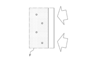
- FIG. 3 is a diagram showing an embodiment of a substrate manufacturing apparatus.
- the substrate manufacturing apparatus is an apparatus that manufactures (that is, processes) a stacked wafer Ws formed by bonding a first wafer W1 and a second wafer W2. Therefore, the substrate manufacturing apparatus may also be called a substrate processing apparatus.
- the substrate manufacturing apparatus fills the gap between the substrate holding device 1 that holds the stacked wafers Ws and the bevel portion B of the first wafer W1 and the bevel portion B of the second wafer W2 (that is, the gap between the stacked wafers Ws).
- a coating device 2 for coating agent F is provided.
- the coating device 2 is arranged above the stacked wafers Ws held in the vertical direction. More specifically, the stacked wafers Ws are held with their planes perpendicular to the horizontal plane. In other words, the stacked wafers Ws are held vertically.
- the coating device 2 includes a supply nozzle 4 that supplies the filler F toward the gaps between the stacked wafers Ws, and a support arm 3 that supports the supply nozzle 4.
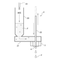
- FIG. 4 is a diagram showing an embodiment of the substrate holding device. As shown in FIG. 4, the substrate holding device 1 is connected to and held by the holding roller 51, and a holding roller 51 that rotates the stacked wafer Ws while holding the peripheral edge of the stacked wafer Ws. A fluid blowing device 60 is provided that blows pressurized fluid to the peripheral edge of the stacked wafer Ws.
- pressurized fluid is a fluid that has been given kinetic energy.
- pressurized fluid means a gas pressurized to the pressure necessary to remove air bubbles from the filler F.
- the substrate holding device 1 By holding the peripheral edge of the stacked wafer Ws with the holding roller 51, it is possible to prevent foreign matter from adhering to the front surface (and back surface) of the stacked wafer Ws.
- the substrate holding device 1 includes four holding rollers 51, but the number of holding rollers 51 is not limited to this embodiment as long as the stacked wafers Ws can be held.
- the substrate holding device 1 holds the stacked wafers Ws vertically, but it may hold the stacked wafers Ws horizontally.
- each holding roller 51 is provided between a first clamping part 53A and a second clamping part 53B that clamp the peripheral edge of the stacked wafer Ws, and a first clamping part 53A and a second clamping part 53B.
- a shaft portion 54 is arranged.
- the substrate holding device 1 includes a roller rotation device 70 that rotates the holding roller 51.
- the roller rotation device 70 includes a connecting rod 71 connected to the holding roller 51 (more specifically, the first clamping part 53A (or the second clamping part 53B)), and a motor 72 that rotates the connecting rod 71. We are prepared.
- the fluid blowout device 60 opens and closes a fluid supply line 61 connected to a blowout port 52 formed on the outer peripheral surface of the shaft portion 54, a fluid supply device 62 connected to the fluid supply line 61, and the fluid supply line 61.
- An on-off valve 63 is provided.
- a plurality of air outlets 52 are formed, but at least one air outlet 52 may be formed.
- the air outlet 52 is formed on the outer peripheral surface of the shaft portion 54 of the holding roller 51. Therefore, when the holding roller 51 holds the stacked wafers Ws, the air outlet 52 faces the gap between the stacked wafers Ws.
- the outlet 52 does not necessarily need to be formed in the shaft portion 54 as long as pressurized fluid can be supplied to the gap between the stacked wafers Ws.
- the fluid blowout device 60 may include a blowout port 52 formed in at least one of the clamping parts 53A and 53B.
- the substrate manufacturing apparatus includes a control device 40 (see FIG. 3) that controls the operation of the roller rotation device 70.
- the control device 40 is electrically connected to the roller rotation device 70 and is configured to rotate the holding roller 51 through the roller rotation device 70.
- the holding roller 51 rotates while the stacked wafer Ws is held by the holding roller 51, the stacked wafer Ws rotates together with the holding roller 51.
- the control device 40 is configured to control the operation of the fluid blowing device 60.
- the control device 40 drives the fluid supply device 62 with the on-off valve 63 open, pressurized fluid is blown out from the outlet 52 through the fluid supply line 61 .
- the control device 40 is configured to control the operation of the coating device 2.
- the control device 40 rotates the stacked wafer Ws through the holding roller 51 by operating the roller rotation device 70, and applies the filler F from above the stacked wafer Ws through the supply nozzle 4 by operating the coating device 2. Let it be supplied.
- the filler F By supplying the filler F while rotating the stacked wafers Ws, the gaps between the stacked wafers Ws are filled with the filler F over the entire circumference of the stacked wafers Ws.
- the substrate holding device 1 has a contact position where the holding roller 51 is brought into contact with the peripheral edge of the stacked wafer Ws, and a separation position where the holding roller 51 is separated from the peripheral edge of the stacked wafer Ws.
- a roller moving device 80 is provided for moving the holding roller 51 between.
- the roller moving device 80 may include a linear actuator coupled to the roller rotating device 70.
- the roller moving device 80 is configured to move the holding roller 51 via the roller rotating device 70.
- the components of the roller moving device 80 are not particularly limited as long as they can move the holding roller 51 between the contact position and the separated position.
- the roller movement device 80 may be a combination of a ball screw and a linear guide.
- the roller moving device 80 moves the holding roller 51 to the contact position. Thereafter, the fluid blowing device 60 removes air bubbles from the filler F applied on the gaps between the stacked wafers Ws. After removing the bubbles, the roller moving device 80 moves the holding roller 51 to the separation position when separating the stacked wafer Ws from the holding roller 51. Thereafter, the stacked wafer Ws is transported to a post-processing module by a transport device (not shown).
- FIGS. 5A and 5B are diagrams showing how pressurized fluid is injected into gaps between stacked wafers. As shown in FIG. 5A, the filler F is compressed by injecting pressurized fluid from the holding roller 51 onto the filler F above the gap between the stacked wafers Ws.
- the air bubbles mixed in the filler F are compressed together with the filler F, and eventually become small to the extent that they do not adversely affect the knife edge portion NE.
- the bubble size reduced by the injection of pressurized fluid does not return to its original size. In this way, the fluid blowing device 60 can remove air bubbles from the filler F applied to the gaps between the stacked wafers Ws.
- the fluid blowing device 60 can remove air bubbles from the filler F applied to the gaps between the stacked wafers Ws. Therefore, the substrate manufacturing apparatus can prevent defects such as cracks and chips from occurring in the knife edge portion NE due to air bubbles mixed in the filler F.
- the fluid blowing device 60 can remove foreign matter (for example, liquid, particles, etc.) attached to the bevel portion B of the wafer W, and can maintain the bevel portion B clean. Therefore, the substrate manufacturing apparatus can prevent defects from occurring in the wafer W due to foreign matter adhering to the bevel portion B of the wafer W.
- foreign matter for example, liquid, particles, etc.
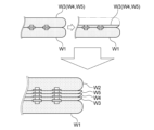
- FIG. 6 is a diagram showing the stacking process of stacked wafers. As shown in FIG. 6, with the wafer W1 and the wafer W3 (W4, W5) bonded together, the back surface of the wafer W3 (W4, W5) is ground (thinned) to perform a grinding process. By repeating such a grinding process and stacking the wafer W3 (W4, W5) on the wafer W1, the thickness of the stacked wafer Ws in the thickness direction increases.
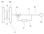
- FIG. 7 is a diagram showing a clamp device that clamps stacked wafers with a holding roller.
- the substrate holding device 1 includes a clamping device 90 that causes the first holding portion 53A and the second holding portion 53B of the holding roller 51 to approach or separate from each other.
- the clamp device 90 includes a first clamp actuator 56A connected to the first clamping part 53A, and a second clamp actuator 56B connected to the second clamping part 53B.
- Each of the clamp actuators 56A and 56B is configured to move each of the clamping parts 53A and 53B in the axial direction of the shaft part 54.
- Each of the clamp actuators 56A, 56B is, for example, a piston rod.
- the control device 40 is configured to control the operation of each of the clamp actuators 56A, 56B.
- the control device 40 can move the clamping parts 53A and 53B toward or away from each other. With such a configuration, the clamp device 90 can clamp stacked wafers Ws having various thicknesses.
- the air outlet 52 is formed on each of the inclined surfaces of the holding parts 53A and 53B. In one embodiment, the air outlet 52 may be formed in the shaft portion 54 . In this embodiment as well, since the blowout port 52 faces the gap between the stacked wafers Ws, the fluid blowout device 60 can remove air bubbles from the filler F applied on the gap between the stacked wafers Ws.
- Filler F is known to have a property of being hardened by heating.
- the filler F is heated to a high temperature (i.e., in order to harden the filler F). It is desirable to heat the filler F by supplying a gas at a required temperature. In other words, the temperature required to cure the filler F is the curing temperature.
- the fluid blowing device 60 may be configured to supply heated fluid heated to a temperature equal to or higher than the curing temperature from at least one of the plurality of holding rollers 51.
- the fluid blowing device 60 may include a heater 67 connected to the fluid supply line 61 (see FIG. 7).
- the heated fluid heated to a temperature higher than the curing temperature is blown out from the outlet 52 of the holding roller 51, and the filler F applied on the gap between the stacked wafers Ws is blown out. harden.
- a pressurized fluid pressurized to the pressure necessary to remove air bubbles from filler F may be heated above the curing temperature and the heated pressurized fluid may be provided. With such a configuration, the fluid blowing device 60 can remove air bubbles and harden the filler F.
- the holding roller 51 adjacent to the coating device 2 and arranged downstream of the coating device 2 in the rotation direction of the stacked wafer Ws will be referred to as a first holding roller 51.
- the holding roller 51 adjacent to the first holding roller 51, which is arranged downstream of the first holding roller 51 in the rotation direction of the stacked wafer Ws is referred to as a second holding roller 51.
- the holding roller 51 adjacent to the second holding roller 51, which is disposed downstream of the second holding roller 51 in the rotation direction of the stacked wafer Ws, is referred to as a third holding roller 51.
- the holding roller 51 adjacent to the third holding roller 51, which is arranged downstream of the third holding roller 51 in the rotation direction of the stacked wafer Ws is referred to as a fourth holding roller 51.
- the fluid blowing device 60 supplies unheated pressurized fluid from each of the first holding roller 51 and the second holding roller 51 to remove air bubbles from the filler F, and removes bubbles from the third holding roller 51 and the second holding roller 51 .
- a heated fluid is supplied from the fourth holding roller 51 to harden the filler F from which air bubbles have been removed.
- the filler F can be cured immediately after the air bubbles are removed from the filler F applied onto the gaps between the stacked wafers Ws. Therefore, the application of the filler F, the removal of air bubbles, and the curing of the filler F can be performed in a short time, and as a result, the processing time of the stacked wafer Ws can be shortened.
- the heated fluid supplied from the third retaining roller 51 and the fourth retaining roller 51 may be pressurized to the pressure necessary to remove air bubbles from the filler F.
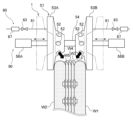
- FIG. 8 is a diagram showing another embodiment of the fluid blowing device.
- the fluid ejection device 60 is configured to switch between unheated pressurized fluid and heated fluid (pressurized fluid or unpressurized fluid).
- the fluid blowing device 60 includes a bypass line 66 branching from the fluid supply line 61, a switching valve 65 connected to the fluid supply line 61 and the bypass line 66, and a heater 67 connected to the bypass line 66. .
- the fluid blowing device 60 configured in this manner is connected to at least one of the plurality of holding rollers 51.
- the fluid blowing device 60 is configured to heat the fluid to be blown onto the peripheral edge of the stacked wafer Ws through a heater 67.
- Controller 40 is configured to control the operation of fluid ejection device 60 .
- the control device 40 operates the switching valve 65 to open the fluid supply line 61 and close the bypass line 66. Due to this operation, the fluid supplied from the fluid supply device 62 is supplied from the outlet 52 without being heated.
- the control device 40 opens the bypass line 66 and closes the upstream side of the fluid supply line 61 (that is, the fluid supply line 61 between the switching valve 65 and the fluid supply device 62) by switching the switching valve 65. Through such an operation, the fluid supplied from the fluid supply device 62 is heated by the heater 67, and the heated pressurized fluid is supplied from the outlet 52.
- FIG. 9 is a diagram showing another embodiment of the coating device.
- the coating device 2 includes a syringe body 20 filled with filler F, an introduction part 21 that introduces the filler F in the syringe body 20 into the supply nozzle 4 through the support arm 3, and an introduction part
- the syringe may include a rod 22 that pushes out the filler F in the syringe body 21 to the supply nozzle 4, and an injection nozzle 23 that injects pressurized fluid (for example, nitrogen gas) to the filler in the syringe body 20.
- pressurized fluid for example, nitrogen gas
- the filler F in the syringe body 20 may already contain air bubbles. Therefore, in the embodiment shown in FIG. 9, the injection nozzle 23 injects pressurized fluid to the filler F supplied to the supply nozzle 4 (that is, the filler F in the syringe main body 20) to form the stacked wafer Ws. It is configured to remove air bubbles from the filler F before it is applied to the gap.
- the control device 40 is configured to be able to control the operation of the injection nozzle 23. More specifically, controller 40 is electrically connected to a fluid source (not shown) that supplies pressurized fluid through injection nozzle 23 . By injecting the pressurized fluid from the injection nozzle 23, the air bubbles mixed into the filler F in the syringe body 20 are compressed together with the filler F, and eventually become small to the extent that they do not adversely affect the knife edge portion NE. (See Figures 5A and 5B).
- the substrate manufacturing apparatus including the substrate holding device 1 is applied to stacked wafers Ws. It is also applicable to W (that is, non-stacked wafers).
- the stacked wafer Ws in this embodiment corresponds to the wafer W, and the peripheral edge of the stacked wafer Ws corresponds to the bevel portion B of the wafer W. Therefore, the bevel portion B of the wafer W means the peripheral portion of the stacked wafer Ws.
- the present invention can be used in a substrate holding device, a substrate manufacturing device, and a substrate manufacturing method.
Landscapes
- Engineering & Computer Science (AREA)
- Physics & Mathematics (AREA)
- Condensed Matter Physics & Semiconductors (AREA)
- General Physics & Mathematics (AREA)
- Manufacturing & Machinery (AREA)
- Computer Hardware Design (AREA)
- Microelectronics & Electronic Packaging (AREA)
- Power Engineering (AREA)
- Container, Conveyance, Adherence, Positioning, Of Wafer (AREA)
Priority Applications (2)
| Application Number | Priority Date | Filing Date | Title |
|---|---|---|---|
| CN202380052721.4A CN119522473A (zh) | 2022-07-13 | 2023-06-15 | 基板保持装置、基板制造装置及基板制造方法 |
| KR1020257004036A KR20250036850A (ko) | 2022-07-13 | 2023-06-15 | 기판 보유 지지 장치, 기판 제조 장치 및 기판 제조 방법 |
Applications Claiming Priority (2)
| Application Number | Priority Date | Filing Date | Title |
|---|---|---|---|
| JP2022-112217 | 2022-07-13 | ||
| JP2022112217A JP2024010749A (ja) | 2022-07-13 | 2022-07-13 | 基板保持装置、基板製造装置、および基板製造方法 |
Publications (1)
| Publication Number | Publication Date |
|---|---|
| WO2024014223A1 true WO2024014223A1 (ja) | 2024-01-18 |
Family
ID=89536422
Family Applications (1)
| Application Number | Title | Priority Date | Filing Date |
|---|---|---|---|
| PCT/JP2023/022255 Ceased WO2024014223A1 (ja) | 2022-07-13 | 2023-06-15 | 基板保持装置、基板製造装置、および基板製造方法 |
Country Status (5)
| Country | Link |
|---|---|
| JP (1) | JP2024010749A (enExample) |
| KR (1) | KR20250036850A (enExample) |
| CN (1) | CN119522473A (enExample) |
| TW (1) | TW202403935A (enExample) |
| WO (1) | WO2024014223A1 (enExample) |
Citations (6)
| Publication number | Priority date | Publication date | Assignee | Title |
|---|---|---|---|---|
| JP2003077879A (ja) * | 2001-09-05 | 2003-03-14 | Ebara Corp | 基板処理装置及び基板処理方法 |
| JP2015126033A (ja) * | 2013-12-25 | 2015-07-06 | 株式会社ディスコ | 洗浄装置および加工装置 |
| JP2019165152A (ja) * | 2018-03-20 | 2019-09-26 | エイブリック株式会社 | 半導体装置及び半導体装置の製造方法及び半導体集積回路装置の製造方法 |
| WO2020153219A1 (ja) * | 2019-01-24 | 2020-07-30 | 東京エレクトロン株式会社 | 加工装置及び加工方法 |
| JP2022036416A (ja) * | 2020-08-24 | 2022-03-08 | 株式会社荏原製作所 | 基板保持回転機構、基板処理装置 |
| JP2022038834A (ja) * | 2020-08-27 | 2022-03-10 | 株式会社荏原製作所 | 基板処理方法、および基板処理装置 |
-
2022
- 2022-07-13 JP JP2022112217A patent/JP2024010749A/ja active Pending
-
2023
- 2023-06-15 KR KR1020257004036A patent/KR20250036850A/ko active Pending
- 2023-06-15 CN CN202380052721.4A patent/CN119522473A/zh active Pending
- 2023-06-15 WO PCT/JP2023/022255 patent/WO2024014223A1/ja not_active Ceased
- 2023-07-10 TW TW112125609A patent/TW202403935A/zh unknown
Patent Citations (6)
| Publication number | Priority date | Publication date | Assignee | Title |
|---|---|---|---|---|
| JP2003077879A (ja) * | 2001-09-05 | 2003-03-14 | Ebara Corp | 基板処理装置及び基板処理方法 |
| JP2015126033A (ja) * | 2013-12-25 | 2015-07-06 | 株式会社ディスコ | 洗浄装置および加工装置 |
| JP2019165152A (ja) * | 2018-03-20 | 2019-09-26 | エイブリック株式会社 | 半導体装置及び半導体装置の製造方法及び半導体集積回路装置の製造方法 |
| WO2020153219A1 (ja) * | 2019-01-24 | 2020-07-30 | 東京エレクトロン株式会社 | 加工装置及び加工方法 |
| JP2022036416A (ja) * | 2020-08-24 | 2022-03-08 | 株式会社荏原製作所 | 基板保持回転機構、基板処理装置 |
| JP2022038834A (ja) * | 2020-08-27 | 2022-03-10 | 株式会社荏原製作所 | 基板処理方法、および基板処理装置 |
Also Published As
| Publication number | Publication date |
|---|---|
| TW202403935A (zh) | 2024-01-16 |
| JP2024010749A (ja) | 2024-01-25 |
| KR20250036850A (ko) | 2025-03-14 |
| CN119522473A (zh) | 2025-02-25 |
Similar Documents
| Publication | Publication Date | Title |
|---|---|---|
| KR101823718B1 (ko) | 기판 반전 장치, 기판 반전 방법 및 박리 시스템 | |
| TWI894340B (zh) | 基板處理方法及基板處理裝置 | |
| JP2008153659A (ja) | 半導体パッケージ製造用のインラインシステム | |
| JP2013247292A (ja) | 接合システム、接合方法、プログラム及びコンピュータ記憶媒体 | |
| WO2024014223A1 (ja) | 基板保持装置、基板製造装置、および基板製造方法 | |
| KR101852200B1 (ko) | 접합 장치 및 접합 방법 | |
| JP2014056910A (ja) | 塗布処理装置、接合システム、塗布処理方法、プログラム及びコンピュータ記憶媒体 | |
| KR102452936B1 (ko) | 임프린트 장치 및 물품 제조 방법 | |
| JP2024010745A (ja) | 基板製造方法および基板製造装置 | |
| JP5207037B2 (ja) | 接着剤注入装置 | |
| US20060180579A1 (en) | Multidirectional cutting chuck | |
| JP6141212B2 (ja) | 処理液ノズル及び塗布処理装置 | |
| KR20240046827A (ko) | 기판 처리 방법 | |
| JP2016136559A (ja) | 被加工物の切削方法 | |
| CN105405753B (zh) | 保护覆盖膜的覆盖方法 | |
| CN117916859A (zh) | 基板处理方法 | |
| JP2024022110A (ja) | 充填剤塗布装置 | |
| JP2023035844A (ja) | 基板処理方法 | |
| WO2024166656A1 (ja) | 基板処理装置 | |
| JP2025024932A (ja) | 積層体の製造方法 | |
| KR20180007331A (ko) | 임프린트 장치 및 물품 제조 방법 | |
| TW202449923A (zh) | 用於形成接合組件的方法及設備 | |
| JP2017030266A (ja) | マイクロデバイスの製造方法 | |
| JP2009253109A (ja) | 積層ウェハ端面のシール形成装置、およびシール形成方法 | |
| JP2008006334A (ja) | 塗布ノズルおよび該ノズルの製造方法 |
Legal Events
| Date | Code | Title | Description |
|---|---|---|---|
| 121 | Ep: the epo has been informed by wipo that ep was designated in this application |
Ref document number: 23839398 Country of ref document: EP Kind code of ref document: A1 |
|
| WWE | Wipo information: entry into national phase |
Ref document number: 202380052721.4 Country of ref document: CN |
|
| ENP | Entry into the national phase |
Ref document number: 20257004036 Country of ref document: KR Kind code of ref document: A |
|
| WWE | Wipo information: entry into national phase |
Ref document number: 1020257004036 Country of ref document: KR |
|
| NENP | Non-entry into the national phase |
Ref country code: DE |
|
| WWP | Wipo information: published in national office |
Ref document number: 202380052721.4 Country of ref document: CN |
|
| WWP | Wipo information: published in national office |
Ref document number: 1020257004036 Country of ref document: KR |
|
| 122 | Ep: pct application non-entry in european phase |
Ref document number: 23839398 Country of ref document: EP Kind code of ref document: A1 |