WO2023286817A1 - 撮像用の光電変換素子用材料 - Google Patents
撮像用の光電変換素子用材料 Download PDFInfo
- Publication number
- WO2023286817A1 WO2023286817A1 PCT/JP2022/027621 JP2022027621W WO2023286817A1 WO 2023286817 A1 WO2023286817 A1 WO 2023286817A1 JP 2022027621 W JP2022027621 W JP 2022027621W WO 2023286817 A1 WO2023286817 A1 WO 2023286817A1
- Authority
- WO
- WIPO (PCT)
- Prior art keywords
- photoelectric conversion
- group
- aromatic
- substituted
- unsubstituted
- Prior art date
- Legal status (The legal status is an assumption and is not a legal conclusion. Google has not performed a legal analysis and makes no representation as to the accuracy of the status listed.)
- Ceased
Links
Images
Classifications
-
- H—ELECTRICITY
- H10—SEMICONDUCTOR DEVICES; ELECTRIC SOLID-STATE DEVICES NOT OTHERWISE PROVIDED FOR
- H10K—ORGANIC ELECTRIC SOLID-STATE DEVICES
- H10K85/00—Organic materials used in the body or electrodes of devices covered by this subclass
- H10K85/60—Organic compounds having low molecular weight
- H10K85/649—Aromatic compounds comprising a hetero atom
- H10K85/657—Polycyclic condensed heteroaromatic hydrocarbons
- H10K85/6572—Polycyclic condensed heteroaromatic hydrocarbons comprising only nitrogen in the heteroaromatic polycondensed ring system, e.g. phenanthroline or carbazole
-
- C—CHEMISTRY; METALLURGY
- C07—ORGANIC CHEMISTRY
- C07D—HETEROCYCLIC COMPOUNDS
- C07D209/00—Heterocyclic compounds containing five-membered rings, condensed with other rings, with one nitrogen atom as the only ring hetero atom
- C07D209/56—Ring systems containing three or more rings
- C07D209/80—[b, c]- or [b, d]-condensed
- C07D209/82—Carbazoles; Hydrogenated carbazoles
- C07D209/86—Carbazoles; Hydrogenated carbazoles with only hydrogen atoms, hydrocarbon or substituted hydrocarbon radicals, directly attached to carbon atoms of the ring system
-
- C—CHEMISTRY; METALLURGY
- C07—ORGANIC CHEMISTRY
- C07D—HETEROCYCLIC COMPOUNDS
- C07D491/00—Heterocyclic compounds containing in the condensed ring system both one or more rings having oxygen atoms as the only ring hetero atoms and one or more rings having nitrogen atoms as the only ring hetero atoms, not provided for by groups C07D451/00 - C07D459/00, C07D463/00, C07D477/00 or C07D489/00
- C07D491/02—Heterocyclic compounds containing in the condensed ring system both one or more rings having oxygen atoms as the only ring hetero atoms and one or more rings having nitrogen atoms as the only ring hetero atoms, not provided for by groups C07D451/00 - C07D459/00, C07D463/00, C07D477/00 or C07D489/00 in which the condensed system contains two hetero rings
- C07D491/04—Ortho-condensed systems
- C07D491/044—Ortho-condensed systems with only one oxygen atom as ring hetero atom in the oxygen-containing ring
- C07D491/048—Ortho-condensed systems with only one oxygen atom as ring hetero atom in the oxygen-containing ring the oxygen-containing ring being five-membered
-
- C—CHEMISTRY; METALLURGY
- C07—ORGANIC CHEMISTRY
- C07D—HETEROCYCLIC COMPOUNDS
- C07D495/00—Heterocyclic compounds containing in the condensed system at least one hetero ring having sulfur atoms as the only ring hetero atoms
- C07D495/02—Heterocyclic compounds containing in the condensed system at least one hetero ring having sulfur atoms as the only ring hetero atoms in which the condensed system contains two hetero rings
- C07D495/04—Ortho-condensed systems
-
- H—ELECTRICITY
- H10—SEMICONDUCTOR DEVICES; ELECTRIC SOLID-STATE DEVICES NOT OTHERWISE PROVIDED FOR
- H10F—INORGANIC SEMICONDUCTOR DEVICES SENSITIVE TO INFRARED RADIATION, LIGHT, ELECTROMAGNETIC RADIATION OF SHORTER WAVELENGTH OR CORPUSCULAR RADIATION
- H10F39/00—Integrated devices, or assemblies of multiple devices, comprising at least one element covered by group H10F30/00, e.g. radiation detectors comprising photodiode arrays
- H10F39/10—Integrated devices
- H10F39/12—Image sensors
-
- H—ELECTRICITY
- H10—SEMICONDUCTOR DEVICES; ELECTRIC SOLID-STATE DEVICES NOT OTHERWISE PROVIDED FOR
- H10K—ORGANIC ELECTRIC SOLID-STATE DEVICES
- H10K30/00—Organic devices sensitive to infrared radiation, light, electromagnetic radiation of shorter wavelength or corpuscular radiation
- H10K30/60—Organic devices sensitive to infrared radiation, light, electromagnetic radiation of shorter wavelength or corpuscular radiation in which radiation controls flow of current through the devices, e.g. photoresistors
-
- H—ELECTRICITY
- H10—SEMICONDUCTOR DEVICES; ELECTRIC SOLID-STATE DEVICES NOT OTHERWISE PROVIDED FOR
- H10K—ORGANIC ELECTRIC SOLID-STATE DEVICES
- H10K30/00—Organic devices sensitive to infrared radiation, light, electromagnetic radiation of shorter wavelength or corpuscular radiation
- H10K30/80—Constructional details
- H10K30/84—Layers having high charge carrier mobility
- H10K30/85—Layers having high electron mobility, e.g. electron-transporting layers or hole-blocking layers
-
- H—ELECTRICITY
- H10—SEMICONDUCTOR DEVICES; ELECTRIC SOLID-STATE DEVICES NOT OTHERWISE PROVIDED FOR
- H10K—ORGANIC ELECTRIC SOLID-STATE DEVICES
- H10K30/00—Organic devices sensitive to infrared radiation, light, electromagnetic radiation of shorter wavelength or corpuscular radiation
- H10K30/80—Constructional details
- H10K30/84—Layers having high charge carrier mobility
- H10K30/86—Layers having high hole mobility, e.g. hole-transporting layers or electron-blocking layers
-
- H—ELECTRICITY
- H10—SEMICONDUCTOR DEVICES; ELECTRIC SOLID-STATE DEVICES NOT OTHERWISE PROVIDED FOR
- H10K—ORGANIC ELECTRIC SOLID-STATE DEVICES
- H10K39/00—Integrated devices, or assemblies of multiple devices, comprising at least one organic radiation-sensitive element covered by group H10K30/00
- H10K39/30—Devices controlled by radiation
- H10K39/32—Organic image sensors
-
- H—ELECTRICITY
- H10—SEMICONDUCTOR DEVICES; ELECTRIC SOLID-STATE DEVICES NOT OTHERWISE PROVIDED FOR
- H10K—ORGANIC ELECTRIC SOLID-STATE DEVICES
- H10K85/00—Organic materials used in the body or electrodes of devices covered by this subclass
- H10K85/20—Carbon compounds, e.g. carbon nanotubes or fullerenes
- H10K85/211—Fullerenes, e.g. C60
-
- H—ELECTRICITY
- H10—SEMICONDUCTOR DEVICES; ELECTRIC SOLID-STATE DEVICES NOT OTHERWISE PROVIDED FOR
- H10K—ORGANIC ELECTRIC SOLID-STATE DEVICES
- H10K85/00—Organic materials used in the body or electrodes of devices covered by this subclass
- H10K85/60—Organic compounds having low molecular weight
- H10K85/615—Polycyclic condensed aromatic hydrocarbons, e.g. anthracene
- H10K85/622—Polycyclic condensed aromatic hydrocarbons, e.g. anthracene containing four rings, e.g. pyrene
-
- H—ELECTRICITY
- H10—SEMICONDUCTOR DEVICES; ELECTRIC SOLID-STATE DEVICES NOT OTHERWISE PROVIDED FOR
- H10K—ORGANIC ELECTRIC SOLID-STATE DEVICES
- H10K85/00—Organic materials used in the body or electrodes of devices covered by this subclass
- H10K85/60—Organic compounds having low molecular weight
- H10K85/631—Amine compounds having at least two aryl rest on at least one amine-nitrogen atom, e.g. triphenylamine
- H10K85/633—Amine compounds having at least two aryl rest on at least one amine-nitrogen atom, e.g. triphenylamine comprising polycyclic condensed aromatic hydrocarbons as substituents on the nitrogen atom
-
- H—ELECTRICITY
- H10—SEMICONDUCTOR DEVICES; ELECTRIC SOLID-STATE DEVICES NOT OTHERWISE PROVIDED FOR
- H10K—ORGANIC ELECTRIC SOLID-STATE DEVICES
- H10K85/00—Organic materials used in the body or electrodes of devices covered by this subclass
- H10K85/60—Organic compounds having low molecular weight
- H10K85/631—Amine compounds having at least two aryl rest on at least one amine-nitrogen atom, e.g. triphenylamine
- H10K85/636—Amine compounds having at least two aryl rest on at least one amine-nitrogen atom, e.g. triphenylamine comprising heteroaromatic hydrocarbons as substituents on the nitrogen atom
-
- H—ELECTRICITY
- H10—SEMICONDUCTOR DEVICES; ELECTRIC SOLID-STATE DEVICES NOT OTHERWISE PROVIDED FOR
- H10K—ORGANIC ELECTRIC SOLID-STATE DEVICES
- H10K85/00—Organic materials used in the body or electrodes of devices covered by this subclass
- H10K85/60—Organic compounds having low molecular weight
- H10K85/649—Aromatic compounds comprising a hetero atom
- H10K85/654—Aromatic compounds comprising a hetero atom comprising only nitrogen as heteroatom
-
- H—ELECTRICITY
- H10—SEMICONDUCTOR DEVICES; ELECTRIC SOLID-STATE DEVICES NOT OTHERWISE PROVIDED FOR
- H10K—ORGANIC ELECTRIC SOLID-STATE DEVICES
- H10K85/00—Organic materials used in the body or electrodes of devices covered by this subclass
- H10K85/60—Organic compounds having low molecular weight
- H10K85/649—Aromatic compounds comprising a hetero atom
- H10K85/657—Polycyclic condensed heteroaromatic hydrocarbons
-
- H—ELECTRICITY
- H10—SEMICONDUCTOR DEVICES; ELECTRIC SOLID-STATE DEVICES NOT OTHERWISE PROVIDED FOR
- H10K—ORGANIC ELECTRIC SOLID-STATE DEVICES
- H10K85/00—Organic materials used in the body or electrodes of devices covered by this subclass
- H10K85/60—Organic compounds having low molecular weight
- H10K85/649—Aromatic compounds comprising a hetero atom
- H10K85/657—Polycyclic condensed heteroaromatic hydrocarbons
- H10K85/6574—Polycyclic condensed heteroaromatic hydrocarbons comprising only oxygen in the heteroaromatic polycondensed ring system, e.g. cumarine dyes
-
- H—ELECTRICITY
- H10—SEMICONDUCTOR DEVICES; ELECTRIC SOLID-STATE DEVICES NOT OTHERWISE PROVIDED FOR
- H10K—ORGANIC ELECTRIC SOLID-STATE DEVICES
- H10K85/00—Organic materials used in the body or electrodes of devices covered by this subclass
- H10K85/60—Organic compounds having low molecular weight
- H10K85/649—Aromatic compounds comprising a hetero atom
- H10K85/657—Polycyclic condensed heteroaromatic hydrocarbons
- H10K85/6576—Polycyclic condensed heteroaromatic hydrocarbons comprising only sulfur in the heteroaromatic polycondensed ring system, e.g. benzothiophene
-
- H—ELECTRICITY
- H10—SEMICONDUCTOR DEVICES; ELECTRIC SOLID-STATE DEVICES NOT OTHERWISE PROVIDED FOR
- H10K—ORGANIC ELECTRIC SOLID-STATE DEVICES
- H10K85/00—Organic materials used in the body or electrodes of devices covered by this subclass
- H10K85/60—Organic compounds having low molecular weight
- H10K85/658—Organoboranes
-
- H—ELECTRICITY
- H10—SEMICONDUCTOR DEVICES; ELECTRIC SOLID-STATE DEVICES NOT OTHERWISE PROVIDED FOR
- H10K—ORGANIC ELECTRIC SOLID-STATE DEVICES
- H10K2101/00—Properties of the organic materials covered by group H10K85/00
- H10K2101/30—Highest occupied molecular orbital [HOMO], lowest unoccupied molecular orbital [LUMO] or Fermi energy values
-
- Y—GENERAL TAGGING OF NEW TECHNOLOGICAL DEVELOPMENTS; GENERAL TAGGING OF CROSS-SECTIONAL TECHNOLOGIES SPANNING OVER SEVERAL SECTIONS OF THE IPC; TECHNICAL SUBJECTS COVERED BY FORMER USPC CROSS-REFERENCE ART COLLECTIONS [XRACs] AND DIGESTS
- Y02—TECHNOLOGIES OR APPLICATIONS FOR MITIGATION OR ADAPTATION AGAINST CLIMATE CHANGE
- Y02E—REDUCTION OF GREENHOUSE GAS [GHG] EMISSIONS, RELATED TO ENERGY GENERATION, TRANSMISSION OR DISTRIBUTION
- Y02E10/00—Energy generation through renewable energy sources
- Y02E10/50—Photovoltaic [PV] energy
- Y02E10/549—Organic PV cells
Definitions
- the present invention relates to a photoelectric conversion element material and a photoelectric conversion element using the same, and more particularly to a photoelectric conversion element material useful for imaging devices.
- Non-Patent Documents 1 and 2 As one of the solutions to such problems of photoelectric conversion elements, photoelectric conversion elements using organic semiconductors instead of inorganic semiconductors are being developed (Non-Patent Documents 1 and 2). This utilizes the property of organic semiconductors that can selectively absorb only light in a specific wavelength range with high sensitivity, and high sensitivity is achieved by stacking photoelectric conversion elements made of organic semiconductors that correspond to the three primary colors of light. There have been proposals to solve the problems of increasing image quality and resolution. An element in which a photoelectric conversion element made of an organic semiconductor and a photoelectric conversion element made of an inorganic semiconductor are laminated has also been proposed (Non-Patent Document 3).
- a photoelectric conversion element using an organic semiconductor has a photoelectric conversion layer made of an organic semiconductor thin film between two electrodes, and if necessary, a hole blocking layer is provided between the photoelectric conversion layer and the two electrodes. It is an element constructed by arranging a layer and/or an electron blocking layer.
- excitons are generated by absorbing light having a desired wavelength in the photoelectric conversion layer, and then holes and electrons are generated by charge separation of the excitons. The holes and electrons then move to each electrode, converting the light into an electrical signal.
- a method of applying a bias voltage between both electrodes is generally used. become one. For this reason, it can be said that controlling the movement of holes and electrons in the photoelectric conversion element is the key to developing the characteristics of the photoelectric conversion element.
- the organic semiconductors used in each layer of the photoelectric conversion element can be roughly divided into P-type organic semiconductors and N-type organic semiconductors.
- P-type organic semiconductors are used as hole-transporting materials
- N-type organic semiconductors are used as electron-transporting materials.
- appropriate physical properties such as hole mobility, electron mobility, highest occupied electron orbital (HOMO) energy value, lowest unoccupied orbital (
- HOMO highest occupied electron orbital
- LUMO lowest unoccupied orbital
- Patent Document 1 discloses an element using quinacridone as a P-type organic semiconductor in a photoelectric conversion layer, subphthalocyanine chloride as an N-type organic semiconductor, and an indolocarbazole derivative in a first buffer layer disposed between a photoelectric conversion layer and an electrode. Proposed.
- Patent Document 2 proposes an element using chrysenodithiophene derivatives as P-type organic semiconductors and fullerenes and subphthalocyanine derivatives as N-type organic semiconductors in the photoelectric conversion layer.
- Patent Documents 3 and 4 propose an element using a carbazole derivative for an electron blocking layer disposed between a photoelectric conversion layer and an electrode.
- Patent Document 5 proposes an element using a pyrene derivative or a triphenylene derivative for an electron blocking layer disposed between a photoelectric conversion layer and an electrode.
- Patent Document 6 proposes an element using a biscarbazole compound or the like for an electron blocking layer.
- JP 2018-85427 A Japanese Patent Application Laid-Open No. 2019-54228 JP 2011-228614 A Japanese Patent Application Laid-Open No. 2021-77888 Japanese Patent Application Laid-Open No. 2015-153910 JP 2011-176259 A
- an object of the present invention is to provide a material that realizes high sensitivity and high resolution of an imaging photoelectric conversion element, and an imaging photoelectric conversion element using the same.
- the present inventors found that the process of generating holes and electrons due to charge separation of excitons in the photoelectric conversion layer and the process of movement of holes and electrons in the photoelectric conversion element were caused by a specific carbazole The inventors have found that the use of a compound can efficiently proceed, and have completed the present invention.
- the present invention provides a material for photoelectric conversion elements for imaging, comprising a carbazole compound represented by the following general formula (1), (2) or (3).
- Ar 1 to Ar 5 are each independently deuterium, a cyano group, a substituted or unsubstituted diarylamino group having 12 to 30 carbon atoms, a substituted or unsubstituted substituted or unsubstituted arylheteroarylamino group having 12 to 30 carbon atoms, substituted or unsubstituted diheteroarylamino group having 12 to 30 carbon atoms, substituted or unsubstituted aromatic hydrocarbon group having 6 to 30 carbon atoms, substituted or Unsubstituted aromatic heterocyclic groups having 3 to 18 carbon atoms, or substituted or unsubstituted linked aromatic groups in which 2 to 6 aromatic rings of these aromatic hydrocarbon groups or aromatic heterocyclic groups are linked and each L 1 is independently a direct bond, a substituted or unsubstituted diarylamino group
- L 1 and Ar 1 to Ar 5 are a group having an aromatic ring structure selected from the following formula (4) or (5), and the aromatic ring structure has a substituent good too.
- L 1 or Ar 1 to Ar 5 are not aromatic heterocyclic groups having 12 or more carbon atoms, except for groups having such an aromatic ring structure.
- ring A is a heterocyclic ring represented by formula (5A), and ring A is condensed with an adjacent ring at any position.
- X 1 is O, S, Se, NR, or N
- X 2 is O, S, or Se.
- R is a substituted or unsubstituted aromatic hydrocarbon group having 6 to 30 carbon atoms, a substituted or unsubstituted aromatic heterocyclic group having 3 to 11 carbon atoms, or 2 to 6 of these aromatic rings linked together is a substituted or unsubstituted linked aromatic group.
- Ar 1 to Ar 5 are each independently deuterium, a substituted or unsubstituted aromatic hydrocarbon group having 6 to 30 carbon atoms, a substituted or unsubstituted aromatic heterocyclic group having 3 to 18 carbon atoms, or It is preferably a substituted or unsubstituted linked aromatic group in which 2 to 6 of these aromatic rings are linked.
- a to f are each 0, g+h, i+j, and k+m are 0 or 1.
- the photoelectric conversion element materials represented by the formulas (1) to (3) are preferable.
- the group having an aromatic ring structure is preferably a group represented by the following formula (4a), (4b), (5a), (5b) or (5c).
- Ring A has the same definition as in formula 5. * indicates a point of attachment, but in formulas (4b), (5b), and (5c), at least two are points of attachment.
- the energy level of the highest occupied molecular orbital (HOMO) obtained by structure optimization calculation by density functional calculation B3LYP/6-31G(d) is ⁇ 4.5 eV or less, or
- the energy level of the lowest unoccupied molecular orbital (LUMO) is preferably -2.5 eV or higher.
- the photoelectric conversion element material preferably has a hole mobility of 1 ⁇ 10 ⁇ 6 cm 2 /Vs or more, or is amorphous.
- the above photoelectric conversion element material can be used as a hole-transporting material.
- the present invention provides an imaging photoelectric conversion element having a photoelectric conversion layer and an electron blocking layer between two electrodes, wherein at least one of the photoelectric conversion layer and the electron blocking layer contains the above photoelectric conversion element material.
- a photoelectric conversion element for imaging characterized by:
- the photoelectric conversion layer can contain an electron-transporting material, and the electron-blocking layer can contain the above photoelectric conversion device material.
- the material for an imaging photoelectric conversion device of the present invention By using the material for an imaging photoelectric conversion device of the present invention, it is possible to realize appropriate movement of holes and electrons in the photoelectric conversion device. It is considered that the leakage current can be reduced, and as a result, a photoelectric conversion element that achieves a low dark current value and a high contrast ratio can be obtained.
- the material of the present invention is useful as a photoelectric conversion element material for a photoelectric conversion film-stacked imaging device.
- the imaging photoelectric conversion element of the present invention is a photoelectric conversion element that has at least one organic layer between two electrodes and converts light into electrical energy.
- the organic layer contains a material for photoelectric conversion elements for imaging represented by any one of the general formulas (1) to (3).
- the photoelectric conversion element material for imaging represented by any one of the above general formulas (1) to (3) is referred to as the photoelectric conversion element material, the material of the present invention, or the general formulas (1) to (3). It is also referred to as a compound represented by
- Ar 1 to Ar 5 each independently deuterium, a cyano group, a substituted or unsubstituted diarylamino group having 12 to 30 carbon atoms, a substituted or unsubstituted 12-30 arylheteroarylamino group, substituted or unsubstituted diheteroarylamino group having 12-30 carbon atoms, substituted or unsubstituted aromatic hydrocarbon group having 6-30 carbon atoms, substituted or unsubstituted carbon It is an aromatic heterocyclic group having a number of 3 to 18, or a substituted or unsubstituted linked aromatic group in which 2 to 6 aromatic rings of these aromatic hydrocarbon groups or aromatic heterocyclic groups are linked.
- Each L 1 is independently a direct bond, a substituted or unsubstituted aromatic hydrocarbon group having 6 to 30 carbon atoms, a substituted or unsubstituted aromatic heterocyclic group having 3 to 18 carbon atoms, or these aromatic It is a substituted or unsubstituted linked aromatic group in which 2 to 6 rings are linked.
- L 1 and Ar 1 to Ar 5 is a group having an aromatic ring structure selected from the above formula (4) or (5), and the aromatic ring structure has a substituent. good too.
- L 1 or Ar 1 to Ar 5 are not aromatic heterocyclic groups having 12 or more carbon atoms, except for groups having such an aromatic ring structure. In the case of a linked aromatic group containing an aromatic heterocyclic group, the linked aromatic group does not contain an aromatic heterocyclic group having 12 or more carbon atoms.
- Ar 1 to Ar 5 are an unsubstituted diarylamino group having 12 to 30 carbon atoms, an unsubstituted arylheteroarylamino group having 12 to 30 carbon atoms, or an unsubstituted diheteroarylamino group having 12 to 30 carbon atoms; Specific examples when represented include diphenylamino, dibiphenylamino, phenylbiphenylamino, naphthylphenylamino, dinaphthylamino, triphenylenephenylamino, dianthranylamino, diphenanethrenylamino, dibenzofuranylphenylamino, dibenzofuran nilbiphenylamino, phenylcarbazolephenylamino, or bisdibenzofuranylamino.
- diphenylamino dibiphenylamino, phenylbiphenylamino, naphthylphenylamino, dinaphthylamino, triphenylenephenylamino, dibenzofuranylphenylamino, dibenzofuranylbiphenylamino and bisdibenzofuranylamino. More preferred are diphenylamino, phenylbiphenylamino, triphenylenephenylamino, dibenzofuranylphenylamino, and dibenzofuranylbiphenylamino.
- the aryl group constituting the amino group is preferably an aryl group having 6 to 18 carbon atoms, and the heteroaryl group is preferably a heteroaryl group having 6 to 15 carbon atoms. These amino groups preferably have 12 to 24 carbon atoms. Moreover, N, S or O is preferable as the heteroatom in the heteroaryl group.
- L 1 and Ar 1 to Ar 5 are substituted or unsubstituted aromatic hydrocarbon groups, substituted or unsubstituted aromatic heterocyclic groups, or substituted or unsubstituted groups in which 2 to 6 of these aromatic rings are linked. It may be a substituted linking aromatic group.
- L 1 is a divalent group and Ar 1 to Ar 5 are monovalent groups, which are selected from the corresponding aromatic hydrocarbon compound, aromatic heterocyclic compound or linked aromatic compound, one or two Since it is a group from which one hydrogen is removed, it will be explained collectively.
- the aromatic hydrocarbon group is an aromatic hydrocarbon from which one or two hydrogens have been removed.
- the aromatic hydrocarbon include monocyclic aromatic hydrocarbons such as benzene, bicyclic aromatic hydrocarbons such as naphthalene, and tricyclic aromatic hydrocarbons such as indacene, biphenylene, phenalene, anthracene, phenanthrene, and fluorene.
- Hydrocarbons fluoranthene, acephenanthrylene, aceanthrylene, triphenylene, pyrene, chrysene, tetraphene, tetracene, tetracyclic aromatic hydrocarbons such as pleiadene, picene, perylene, pentaphene, pentacene, tetraphenylene, naphthanthracene and pentacyclic aromatic hydrocarbons such as Benzene, naphthalene, anthracene, triphenylene, or pyrene are preferred.
- the aromatic heterocyclic group includes one or two hydrogen atoms from the aromatic heterocyclic compound.
- the aromatic heterocyclic compound include nitrogen-containing aromatic compounds having a pyrrole ring such as pyrrole, pyrrolopyrrole, indole, isoindole, pyrroloisoindole, carboline, thiophene, benzothiophene, furan, benzofuran, pyridine, pyrimidine , triazines, quinolines, isoquinolines, quinazolines or quinoxalines may be mentioned by way of example.
- the group having an aromatic ring structure represented by the above formula (4) or formula (5) may have a substituent, and may be included as one aromatic group constituting a linked aromatic group. good.
- a triphenylene group is preferably exemplified.
- a group in which X 1 is N is preferably exemplified.
- a linked aromatic group refers to an aromatic group in which two or more aromatic rings of aromatic groups are linked by single bonds. These linking aromatic groups may be linear or branched. The connection position when the benzene rings are connected to each other may be ortho, meta, or para.
- the aromatic group may be an aromatic hydrocarbon group or an aromatic heterocyclic group, and plural aromatic groups may be the same or different.
- the aromatic ring that constitutes the linked aromatic group is the aromatic ring that the aromatic hydrocarbon group or aromatic heterocyclic group has, and these aromatic rings are linked by a single bond.
- the number of bonded aromatic rings is 2 to 6, preferably 2 to 5.
- the aromatic ring of the aromatic hydrocarbon group or aromatic heterocyclic group is preferably benzene, naphthalene, anthracene, triphenylene, pyrene, thiophene, benzothiophene, furan, benzofuran, pyridine, pyrimidine, triazine, quinoline,
- the diarylamino group, arylheteroarylamino group, diheteroarylamino group, aromatic hydrocarbon group, aromatic heterocyclic group, or linking aromatic group may have a substituent.
- Substituents include deuterium, cyano group, diarylamino group having 12 to 30 carbon atoms, arylheteroarylamino group having 12 to 30 carbon atoms, diheteroarylamino group having 12 to 30 carbon atoms, and 1 to 20 carbon atoms. can be mentioned.
- Specific examples of a diarylamino group, an arylheteroarylamino group, and a diheteroarylamino group refer to cases where Ar 1 to Ar 5 are these.
- the alkyl group having 1 to 20 carbon atoms may be a linear, branched or cyclic alkyl group, preferably a linear, branched or cyclic alkyl group having 1 to 10 carbon atoms. Specific examples thereof include methyl group, ethyl group, n-propyl group, n-butyl group, n-pentyl group, n-hexyl group, n-octyl group, n-dodecyl group, n-tetradecyl group and n-octadecyl group.
- linear saturated hydrocarbon groups such as isopropyl group, isobutyl group, neopentyl group, 2-ethylhexyl group, branched saturated hydrocarbon groups such as 2-hexyloctyl group, cyclopentyl group, cyclohexyl group, cyclooctyl group, 4-butylcyclohexyl and saturated alicyclic hydrocarbon groups such as 4-dodecylcyclohexyl group.
- Preferred embodiments of general formula (1) include the following formulas (1a) to (1f), with formulas (1d) to (1f) being more preferred.
- symbols common to general formula (1) have the same meanings.
- Preferred embodiments of general formula (2) include the following formulas (2a) to (2c), with formulas (2a) and (2c) being more preferred.
- symbols common to general formula (2) have the same meanings.
- At least one of L 1 and Ar 1 to Ar 5 has an aromatic ring structure selected from the above formula (4)
- at least one of L 1 and Ar 2 to Ar 5 is an aromatic ring of formula (4) structure, and more preferably at least one of L 1 , Ar 4 and Ar 5 has the aromatic ring structure of formula (4).
- at least one of L 1 or Ar 1 to Ar 5 has the aromatic ring structure of the above formula (5)
- at least one of L 1 and Ar 2 to Ar 5 has the aromatic ring structure of the above formula (5) and more preferably at least one of Ar 4 and Ar 5 has the aromatic ring structure of formula (5).
- ring A is a heterocyclic ring represented by formula (5A), and ring A is condensed with an adjacent ring at any position.
- X 1 is O, S, Se, NR, or N
- X 2 is O, S, or Se
- X 1 is preferably NR or N
- X 2 is preferably O or S.
- N it can be attached to the carbazole ring at the N position.
- R is a substituted or unsubstituted aromatic hydrocarbon group having 6 to 30 carbon atoms, a substituted or unsubstituted aromatic heterocyclic group having 3 to 11 carbon atoms, or 2 to 6 of these aromatic rings linked together is a substituted or unsubstituted linked aromatic group.
- Examples of the unsubstituted aromatic hydrocarbon group having 6 to 30 carbon atoms include a group obtained by removing one hydrogen from an aromatic hydrocarbon.
- Examples of the aromatic hydrocarbon include monocyclic aromatic hydrocarbons such as benzene, bicyclic aromatic hydrocarbons such as naphthalene, and tricyclic aromatic hydrocarbons such as indacene, biphenylene, phenalene, anthracene, phenanthrene, and fluorene.
- Hydrocarbons fluoranthene, acephenanthrylene, aceanthrylene, triphenylene, pyrene, chrysene, tetraphene, tetracene, tetracyclic aromatic hydrocarbons such as pleiadene, picene, perylene, pentaphene, pentacene, tetraphenylene, naphthanthracene and pentacyclic aromatic hydrocarbons such as Benzene, naphthalene, anthracene, triphenylene, or pyrene are preferred.
- the unsubstituted aromatic heterocyclic group having 3 to 11 carbon atoms a group obtained by removing one or two hydrogen atoms from an aromatic heterocyclic compound can be used.
- the aromatic heterocyclic compound include pyrrole, pyrrolopyrrole, indole, pyrroloindole, benzoindole, naphthopyrrole, isoindole, pyrroloisoindole, benzisoindole, naphthoisopyrrole, and carboline. Nitrogen aromatic compounds and the like can be mentioned. Thiophene, benzothiophene, furan, benzofuran, pyridine, pyrimidine, triazine, quinoline, isoquinoline, quinazoline, or quinoxaline are preferred.
- R is an aromatic hydrocarbon group or an aromatic heterocyclic group, it may have a substituent. is similar to
- the aromatic ring structure of formula (4) or formula (5) has one or more bonding points (or bonds; represented by *). When it has a substituent or when it is included as a constituent unit of a linked aromatic group, it has a plurality of bonds. Otherwise, L 1 has two bonds and Ar 1 to Ar 5 has one bond. And it can be combined at any position.
- formulas (4a), (4b), (4c), (5a), (5b) or (5c) are preferred.
- formulas (4a) and (5a) are monovalent groups, and correspond to this when Ar 1 to Ar 5 have one bond.
- Formulas (4b), (5b) and (5c) are groups having a valence of 2 or more, and in the case of divalence, this applies when L 1 has two bonds.
- Formula (4c) is a divalent group, and it can be said to be a preferred embodiment when formula (4b) is a divalent group.
- the substituent when it has a substituent, it is preferably bonded to the substituent at the bonding point represented by the above formula (4a), (4b), (5a), (5b) or (5c). It may be a connection point.
- the aromatic ring structure as a component of the linking aromatic group, it is preferable to link at the above-mentioned bonding point or to bond with the carbazolyl group at the terminal.
- the above formula (4a) is a case where the group having the formula (4) as an aromatic ring structure is a monovalent group, and the above formula (4b) is a case where it is a divalent or higher group.
- the above formula (5a) is a case where the group having the formula (5) as an aromatic ring structure is a monovalent group, and the above formula (5b) or (5c) is a case where it is a divalent or higher group.
- * in formula (4b), (5b) or (5c) is a bonding point, but when the number of bonds is 2 or less, the remaining * represents hydrogen (or a bonding point with a substituent).
- a group having an aromatic ring structure of formula (4) above is preferably represented by any one of formulas (4a) and (4c) to (4g) below. (4a) or (4c) is more preferred. * is the attachment point.
- ring A can be bonded at any position, but the structure represented by formula (5a), (5b) or (5c) is preferred.
- Ring A is represented by formula (5A), and X2 is O, S, or Se.
- the formula (5a) is a monovalent group, and the formula (5b) or (5c) is a divalent or higher group, but the divalent or higher group is preferably the formula (5b).
- Equation (5b) is the case where X1 in Equation ( 5 ) is N.
- formula (5c) when X 1 is NR, it can be attached on R.
- the group When the group has an aromatic ring structure of formula (5) and has two or more bonding points, it may have a structure having a plurality of bonding points in the same benzene ring.
- the aromatic ring structure of the above formula (5) is represented by the following formulas (5k) to (5q), preferably formula (5k), formula (5l), formula (5n), formula (5p), or formula ( 5q), more preferably represented by formula (5k), formula (5n), or formula (5q).
- a to m are each independently an integer of 0 to 3.
- a to f are preferably 0 and g+h, i+j and k+m are preferably 0 or 1.
- the photoelectric conversion element material of the present invention is an organic compound containing coupling reactions such as Suzuki coupling, Stille coupling, Grignard coupling, Ullmann coupling, Buchwald-Hartwig reaction and Heck reaction using commercially available reagents as raw materials. It can be obtained by synthesizing by a method based on various organic synthesis reactions established in the field of synthetic chemistry, and then purifying using a known method such as recrystallization, column chromatography, and sublimation purification. It is not limited.
- the energy level of the highest occupied molecular orbital (HOMO) obtained by structure optimization calculation by density functional calculation B3LYP/6-31G(D) is ⁇ 4.5 eV or less. is preferred, and more preferably in the range of -4.5 eV to -6.0 eV.
- the energy level of the lowest unoccupied molecular orbital (LUMO) obtained by structure optimization calculation by density functional calculation B3LYP/6-31G(D) is -2.5 eV or higher. It is preferably in the range of -2.5 eV to -0.5 eV.
- the difference (absolute value) between the HOMO energy level and the LUMO energy level is preferably in the range of 2.0 to 5.0 eV, more preferably 2.5 to 4.0 eV. It is in the range of 0 eV.
- the photoelectric conversion element material of the present invention preferably has a hole mobility of 1 ⁇ 10 ⁇ 6 cm 2 /Vs to 1 cm 2 /Vs, more preferably 1 ⁇ 10 ⁇ 5 cm 2 /Vs to 1 ⁇ 10 ⁇ 6 cm 2 /Vs to 1 cm 2 /Vs. It has a hole mobility of 10 ⁇ 1 cm 2 /Vs. Hole mobility can be evaluated by known methods such as a method using an FET type transistor element, a method using a time-of-flight method, and an SCLC method.
- the material for photoelectric conversion elements of the present invention is preferably amorphous. Amorphousness can be confirmed by various methods. For example, it can be confirmed by detecting no peak by the XRD method or detecting no endothermic peak by the DSC method.
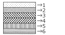
- FIG. 1 is a cross-sectional view schematically showing the structure of an imaging photoelectric conversion element using the imaging photoelectric conversion element material of the present invention, wherein 1 is a substrate, 2 is an electrode, 3 is an electron blocking layer, and 4 is a photoelectric conversion. Layers 5 are hole blocking layers and 6 are electrodes.
- the structure is not limited to that of FIG. 1, and layers can be added or omitted as needed. It is also possible to have a structure opposite to that of FIG. can be added or omitted.
- the layers constituting the laminated structure on the substrate other than the electrodes such as the anode and the cathode are sometimes collectively referred to as the organic layer.
- the electrode used in the imaging photoelectric conversion element of the present invention has a function of collecting holes and electrons generated in the photoelectric conversion layer. In addition, a function of allowing light to enter the photoelectric conversion layer is also required. Therefore, it is desirable that at least one of the two electrodes is transparent or translucent.
- the material used as the electrode is not particularly limited as long as it has conductivity. gallium-doped zinc oxide), conductive transparent materials such as TiO2 and FTO, metals such as gold, silver, platinum, chromium, aluminum, iron, cobalt, nickel and tungsten, inorganic conductive materials such as copper iodide and copper sulfide , polythiophene, polypyrrole and polyaniline. These materials may be used in combination if necessary. Moreover, you may laminate
- the photoelectric conversion layer is a layer in which holes and electrons are generated by charge separation of excitons generated by incident light. Although it may be formed of a single photoelectric conversion material, it may be formed in combination with a P-type organic semiconductor material that is a hole-transporting material or an N-type organic semiconductor material that is an electron-transporting material. Also, two or more P-type organic semiconductors may be used, and two or more N-type organic semiconductors may be used. For one or more of these P-type organic semiconductors and/or N-type semiconductors, it is desirable to use a dye material having a function of absorbing light of a desired wavelength in the visible region.
- the material for photoelectric conversion elements of the present invention can be used as a P-type organic semiconductor material that is a hole-transporting material.
- any material having a hole-transporting property may be used, and it is preferable to use the photoelectric conversion element material of the present invention, but other P-type organic semiconductor materials may be used. Also, two or more compounds represented by the above formulas (1) to (3) may be mixed and used. Further, the above compound and other P-type organic semiconductor materials may be mixed and used.
- P-type organic semiconductor materials may be any material that has a hole-transporting property.
- polyphenylenevinylene derivatives polyparaphenylene derivatives, polyfluorene derivatives, polyvinylcarbazole derivatives, and polythiophene derivatives can be exemplified as polymeric P-type organic semiconductor materials.
- polymeric P-type organic semiconductor materials two or more selected from compounds represented by the formulas (1) to (3) of the present invention, P-type organic semiconductor materials, and polymeric P-type organic semiconductor materials may be mixed and used.
- N-type organic semiconductor material any material having an electron-transporting property can be used. and the like can be exemplified. Also, two or more selected from N-type organic semiconductor materials may be mixed and used.
- the electron blocking layer is provided to suppress dark current caused by injection of electrons from one of the electrodes into the photoelectric conversion layer when a bias voltage is applied between the two electrodes. It also has a hole transport function for transporting holes generated by charge separation in the photoelectric conversion layer to the electrode, and a single layer or multiple layers can be arranged as necessary.
- a P-type organic semiconductor material which is a hole-transporting material, can be used for the electron blocking layer.
- the P-type organic semiconductor material any material having a hole-transporting property may be used, and it is preferable to use the compounds represented by the above formulas (1) to (3), but other P-type organic semiconductor materials may be used. may Also, the compounds represented by the formulas (1) to (3) may be mixed with other P-type organic semiconductor materials or polymeric P-type organic semiconductor materials as described above.
- the hole-blocking layer is provided to suppress dark current caused by injection of holes from one of the electrodes into the photoelectric conversion layer when a bias voltage is applied between the two electrodes. It also has an electron transport function of transporting electrons generated by charge separation in the photoelectric conversion layer to the electrode, and a single layer or multiple layers can be arranged as necessary.
- An N-type organic semiconductor having an electron transport property can be used for the hole blocking layer.
- the N-type organic semiconductor material any material having an electron-transporting property may be used.
- azole derivatives such as imidazole, thiazole, thiadiazole, oxazole, oxadiazole, triazole, tris(8-quinolinolato) aluminum (III) derivatives, phosphine oxide derivatives, nitro-substituted fluorene derivatives, diphenylquinone derivatives, Thiopyran dioxide derivatives, carbodiimides, phthalenylidenemethane derivatives, anthraquinodimethane and anthrone derivatives, bipyridine derivatives, quinoline derivatives, indoloca.BR>O sol derivatives and the like can be mentioned. Also, two or more selected from N-type organic semiconductor materials may be mixed and used.
- the hydrogen in the materials of the invention may be deuterium. That is, in addition to the hydrogen on the aromatic rings in the general formulas (1) to (5), some or all of the hydrogens on the aromatic rings of Ar 1 to Ar 6 , L 1 and R are deuterium. may Furthermore, part or all of the hydrogen contained in the compounds used as the N-type organic semiconductor material and the P-type organic semiconductor material may be deuterium.
- each layer when producing the imaging photoelectric conversion element of the present invention is not particularly limited, and may be produced by either a dry process or a wet process. If necessary, the organic layer containing the photoelectric conversion element material of the present invention can be formed into a plurality of layers.
- Synthesis examples of compounds 1, 33, 60, and 93 are shown below as representative examples. Other compounds were synthesized in a similar manner.
- Example 1 A 100 nm-thick film of Compound 93 was formed as an electron blocking layer at a degree of vacuum of 4.0 ⁇ 10 ⁇ 5 Pa on a glass substrate on which electrodes made of ITO with a thickness of 70 nm were formed. Next, as a photoelectric conversion layer, a thin film of quinacridone was formed to a thickness of 100 nm. Finally, a film of aluminum was formed to a thickness of 70 nm as an electrode to prepare a photoelectric conversion element. The current in the dark was 2.5 ⁇ 10 ⁇ 10 A/cm 2 when a voltage of 2 V was applied using ITO and aluminum as electrodes.
- the current was 1.4 ⁇ 10 ⁇ 7 A/cm 2 .
- the contrast ratio was 5.6 ⁇ 10 2 when a voltage of 2 V was applied to the transparent conductive glass side.
- Comparative example 1 A 100-nm-thick film of Compound H1 was formed as an electron-blocking layer at a degree of vacuum of 4.0 ⁇ 10 ⁇ 5 Pa on a glass substrate on which electrodes made of ITO with a thickness of 70 nm were formed. Next, quinacridone was deposited to a thickness of 100 nm as a photoelectric conversion layer. Finally, a film of aluminum was formed to a thickness of 70 nm as an electrode to prepare a photoelectric conversion element. When a voltage of 2 V was applied using ITO and aluminum as electrodes, the current in the dark was 5.6 ⁇ 10 ⁇ 9 A/cm 2 .
- the current was 1.2 ⁇ 10 ⁇ 7 A/cm 2 when a voltage of 2 V was applied to the ITO electrode side and light irradiation was performed with an irradiation light wavelength of 500 nm.
- the contrast ratio when a voltage of 2 V was applied to the transparent conductive glass side was 0.21 ⁇ 10 2 .
- Example 2 A 10-nm-thick film of compound 1 was formed as an electron-blocking layer at a degree of vacuum of 4.0 ⁇ 10 ⁇ 5 Pa on a 70-nm-thick ITO electrode formed on a glass substrate. Then, as a photoelectric conversion layer, 2Ph-BTBT, F6-SubPc-OC6F5, and fullerene (C60) were co-deposited to a thickness of 200 nm at a deposition rate ratio of 4:4:2 to form a film. Subsequently, 10 nm of dpy-NDI was deposited to form a hole blocking layer. Finally, a film of aluminum was formed to a thickness of 70 nm as an electrode to produce a photoelectric conversion element.
- 2Ph-BTBT, F6-SubPc-OC6F5 fullerene
- Examples 3-13 A photoelectric conversion device was produced in the same manner as in Example 2 except that the compounds shown in Table 3 were used as the electron blocking layer.
- Comparative Examples 2-3 A photoelectric conversion device was produced in the same manner as in Example 2 except that the compounds shown in Table 3 were used as the electron blocking layer. Table 3 shows the results of Examples 2-13 and Comparative Examples 2-3.
- the material for an imaging photoelectric conversion device of the present invention By using the material for an imaging photoelectric conversion device of the present invention, it is possible to realize appropriate movement of holes and electrons in the photoelectric conversion device. It is considered that the leakage current can be reduced, and as a result, a photoelectric conversion element that achieves a low dark current value and a high contrast ratio can be obtained.
- the material of the present invention is useful as a photoelectric conversion element material for a photoelectric conversion film-stacked imaging device.
- Electrode 1 Substrate, 2 Electrode, 3 Electron Blocking Layer, 4 Photoelectric Conversion Layer, 5 Hole Blocking Layer, 6 Electrode
Landscapes
- Chemical & Material Sciences (AREA)
- Physics & Mathematics (AREA)
- Engineering & Computer Science (AREA)
- Materials Engineering (AREA)
- Spectroscopy & Molecular Physics (AREA)
- Organic Chemistry (AREA)
- Electromagnetism (AREA)
- Nanotechnology (AREA)
- Light Receiving Elements (AREA)
- Heterocyclic Carbon Compounds Containing A Hetero Ring Having Oxygen Or Sulfur (AREA)
Priority Applications (4)
| Application Number | Priority Date | Filing Date | Title |
|---|---|---|---|
| JP2023534844A JPWO2023286817A1 (https=) | 2021-07-15 | 2022-07-13 | |
| CN202280047446.2A CN117616897A (zh) | 2021-07-15 | 2022-07-13 | 摄像用的光电转换元件用材料 |
| KR1020237044115A KR20240035756A (ko) | 2021-07-15 | 2022-07-13 | 촬상용 광전 변환 소자용 재료 |
| US18/565,774 US20240276746A1 (en) | 2021-07-15 | 2022-07-13 | Material for photoelectric conversion elements for image pickup |
Applications Claiming Priority (2)
| Application Number | Priority Date | Filing Date | Title |
|---|---|---|---|
| JP2021-117404 | 2021-07-15 | ||
| JP2021117404 | 2021-07-15 |
Publications (1)
| Publication Number | Publication Date |
|---|---|
| WO2023286817A1 true WO2023286817A1 (ja) | 2023-01-19 |
Family
ID=84919349
Family Applications (1)
| Application Number | Title | Priority Date | Filing Date |
|---|---|---|---|
| PCT/JP2022/027621 Ceased WO2023286817A1 (ja) | 2021-07-15 | 2022-07-13 | 撮像用の光電変換素子用材料 |
Country Status (6)
| Country | Link |
|---|---|
| US (1) | US20240276746A1 (https=) |
| JP (1) | JPWO2023286817A1 (https=) |
| KR (1) | KR20240035756A (https=) |
| CN (1) | CN117616897A (https=) |
| TW (1) | TW202311238A (https=) |
| WO (1) | WO2023286817A1 (https=) |
Citations (6)
| Publication number | Priority date | Publication date | Assignee | Title |
|---|---|---|---|---|
| JP2011176259A (ja) * | 2009-06-03 | 2011-09-08 | Fujifilm Corp | 光電変換素子及び撮像素子 |
| CN102757300A (zh) * | 2012-05-31 | 2012-10-31 | 吉林奥来德光电材料股份有限公司 | 一种苯并菲衍生物、制备方法及由其制成的发光器件 |
| JP2015153910A (ja) * | 2014-02-14 | 2015-08-24 | 富士フイルム株式会社 | 光電変換素子、光センサおよび撮像素子 |
| JP2017011113A (ja) * | 2015-06-23 | 2017-01-12 | 三星ディスプレイ株式會社Samsung Display Co.,Ltd. | 有機電界発光素子 |
| CN108948008A (zh) * | 2018-08-03 | 2018-12-07 | 瑞声科技(南京)有限公司 | 一种咔唑化合物及其应用 |
| JP2019054499A (ja) * | 2017-02-03 | 2019-04-04 | パナソニックIpマネジメント株式会社 | 撮像装置 |
Family Cites Families (4)
| Publication number | Priority date | Publication date | Assignee | Title |
|---|---|---|---|---|
| EP2306541B1 (en) | 2009-09-11 | 2018-10-24 | Fujifilm Corporation | Photoelectric conversion device, production method thereof, photosensor, imaging device and their drive methods |
| JP6834400B2 (ja) | 2016-11-22 | 2021-02-24 | ソニー株式会社 | 撮像素子、積層型撮像素子、撮像装置及び電子装置 |
| JP7109240B2 (ja) | 2017-09-15 | 2022-07-29 | ソニーセミコンダクタソリューションズ株式会社 | 光電変換素子および固体撮像装置 |
| KR102876927B1 (ko) | 2019-11-06 | 2025-10-24 | 삼성전자주식회사 | 광전 변환 소자, 센서 및 전자 장치 |
-
2022
- 2022-07-13 KR KR1020237044115A patent/KR20240035756A/ko active Pending
- 2022-07-13 JP JP2023534844A patent/JPWO2023286817A1/ja active Pending
- 2022-07-13 CN CN202280047446.2A patent/CN117616897A/zh active Pending
- 2022-07-13 TW TW111126343A patent/TW202311238A/zh unknown
- 2022-07-13 US US18/565,774 patent/US20240276746A1/en active Pending
- 2022-07-13 WO PCT/JP2022/027621 patent/WO2023286817A1/ja not_active Ceased
Patent Citations (6)
| Publication number | Priority date | Publication date | Assignee | Title |
|---|---|---|---|---|
| JP2011176259A (ja) * | 2009-06-03 | 2011-09-08 | Fujifilm Corp | 光電変換素子及び撮像素子 |
| CN102757300A (zh) * | 2012-05-31 | 2012-10-31 | 吉林奥来德光电材料股份有限公司 | 一种苯并菲衍生物、制备方法及由其制成的发光器件 |
| JP2015153910A (ja) * | 2014-02-14 | 2015-08-24 | 富士フイルム株式会社 | 光電変換素子、光センサおよび撮像素子 |
| JP2017011113A (ja) * | 2015-06-23 | 2017-01-12 | 三星ディスプレイ株式會社Samsung Display Co.,Ltd. | 有機電界発光素子 |
| JP2019054499A (ja) * | 2017-02-03 | 2019-04-04 | パナソニックIpマネジメント株式会社 | 撮像装置 |
| CN108948008A (zh) * | 2018-08-03 | 2018-12-07 | 瑞声科技(南京)有限公司 | 一种咔唑化合物及其应用 |
Also Published As
| Publication number | Publication date |
|---|---|
| CN117616897A (zh) | 2024-02-27 |
| US20240276746A1 (en) | 2024-08-15 |
| KR20240035756A (ko) | 2024-03-18 |
| JPWO2023286817A1 (https=) | 2023-01-19 |
| TW202311238A (zh) | 2023-03-16 |
Similar Documents
| Publication | Publication Date | Title |
|---|---|---|
| JP7811552B2 (ja) | 撮像用の光電変換素子材料及び光電変換素子 | |
| KR20250127290A (ko) | 광전 변환 소자용 재료를 포함하는 광전 변환 소자 | |
| WO2024195391A1 (ja) | 光電変換素子 | |
| TWI899379B (zh) | 攝像用光電轉換元件 | |
| WO2023286817A1 (ja) | 撮像用の光電変換素子用材料 | |
| WO2023068217A1 (ja) | 撮像用の光電変換素子用材料及び光電変換素子 | |
| WO2023286816A1 (ja) | 撮像用の光電変換素子用材料及び撮像用光電変換素子 | |
| WO2024057958A1 (ja) | 光電変換素子用材料及び光電変換素子 | |
| WO2025018227A1 (ja) | 光電変換素子用材料及びこれを用いた光電変換素子 | |
| WO2024057957A1 (ja) | 光電変換素子用材料及びこれを用いた光電変換素子 | |
| KR20240137040A (ko) | 촬상용의 광전 변환 소자용 재료 및 광전 변환 소자 | |
| CN120345381A (zh) | 包含光电转换元件用材料的光电转换元件 | |
| WO2023228974A1 (ja) | 撮像用の光電変換素子用材料及びこれを用いた撮像用光電変換素子 | |
| WO2023228922A1 (ja) | 撮像用の光電変換素子用材料及び光電変換素子 |
Legal Events
| Date | Code | Title | Description |
|---|---|---|---|
| DPE1 | Request for preliminary examination filed after expiration of 19th month from priority date (pct application filed from 20040101) | ||
| WWE | Wipo information: entry into national phase |
Ref document number: 18565774 Country of ref document: US |
|
| WWE | Wipo information: entry into national phase |
Ref document number: 2023534844 Country of ref document: JP |
|
| WWE | Wipo information: entry into national phase |
Ref document number: 202280047446.2 Country of ref document: CN |
|
| NENP | Non-entry into the national phase |
Ref country code: DE |
|
| 122 | Ep: pct application non-entry in european phase |
Ref document number: 22842159 Country of ref document: EP Kind code of ref document: A1 |