WO2023281353A1 - トランジスタ - Google Patents
トランジスタ Download PDFInfo
- Publication number
- WO2023281353A1 WO2023281353A1 PCT/IB2022/055967 IB2022055967W WO2023281353A1 WO 2023281353 A1 WO2023281353 A1 WO 2023281353A1 IB 2022055967 W IB2022055967 W IB 2022055967W WO 2023281353 A1 WO2023281353 A1 WO 2023281353A1
- Authority
- WO
- WIPO (PCT)
- Prior art keywords
- insulator
- oxide
- conductor
- transistor
- oxygen
- Prior art date
- Legal status (The legal status is an assumption and is not a legal conclusion. Google has not performed a legal analysis and makes no representation as to the accuracy of the status listed.)
- Ceased
Links
Images
































Classifications
-
- H—ELECTRICITY
- H10—SEMICONDUCTOR DEVICES; ELECTRIC SOLID-STATE DEVICES NOT OTHERWISE PROVIDED FOR
- H10D—INORGANIC ELECTRIC SEMICONDUCTOR DEVICES
- H10D30/00—Field-effect transistors [FET]
- H10D30/60—Insulated-gate field-effect transistors [IGFET]
- H10D30/67—Thin-film transistors [TFT]
- H10D30/6729—Thin-film transistors [TFT] characterised by the electrodes
- H10D30/673—Thin-film transistors [TFT] characterised by the electrodes characterised by the shapes, relative sizes or dispositions of the gate electrodes
- H10D30/6733—Multi-gate TFTs
- H10D30/6734—Multi-gate TFTs having gate electrodes arranged on both top and bottom sides of the channel, e.g. dual-gate TFTs
-
- H—ELECTRICITY
- H10—SEMICONDUCTOR DEVICES; ELECTRIC SOLID-STATE DEVICES NOT OTHERWISE PROVIDED FOR
- H10B—ELECTRONIC MEMORY DEVICES
- H10B12/00—Dynamic random access memory [DRAM] devices
- H10B12/30—DRAM devices comprising one-transistor - one-capacitor [1T-1C] memory cells
- H10B12/31—DRAM devices comprising one-transistor - one-capacitor [1T-1C] memory cells having a storage electrode stacked over the transistor
-
- H—ELECTRICITY
- H10—SEMICONDUCTOR DEVICES; ELECTRIC SOLID-STATE DEVICES NOT OTHERWISE PROVIDED FOR
- H10B—ELECTRONIC MEMORY DEVICES
- H10B12/00—Dynamic random access memory [DRAM] devices
-
- H—ELECTRICITY
- H10—SEMICONDUCTOR DEVICES; ELECTRIC SOLID-STATE DEVICES NOT OTHERWISE PROVIDED FOR
- H10B—ELECTRONIC MEMORY DEVICES
- H10B12/00—Dynamic random access memory [DRAM] devices
- H10B12/01—Manufacture or treatment
- H10B12/02—Manufacture or treatment for one transistor one-capacitor [1T-1C] memory cells
- H10B12/05—Making the transistor
-
- H—ELECTRICITY
- H10—SEMICONDUCTOR DEVICES; ELECTRIC SOLID-STATE DEVICES NOT OTHERWISE PROVIDED FOR
- H10B—ELECTRONIC MEMORY DEVICES
- H10B12/00—Dynamic random access memory [DRAM] devices
- H10B12/30—DRAM devices comprising one-transistor - one-capacitor [1T-1C] memory cells
-
- H—ELECTRICITY
- H10—SEMICONDUCTOR DEVICES; ELECTRIC SOLID-STATE DEVICES NOT OTHERWISE PROVIDED FOR
- H10D—INORGANIC ELECTRIC SEMICONDUCTOR DEVICES
- H10D30/00—Field-effect transistors [FET]
- H10D30/60—Insulated-gate field-effect transistors [IGFET]
- H10D30/67—Thin-film transistors [TFT]
- H10D30/6704—Thin-film transistors [TFT] having supplementary regions or layers in the thin films or in the insulated bulk substrates for controlling properties of the device
-
- H—ELECTRICITY
- H10—SEMICONDUCTOR DEVICES; ELECTRIC SOLID-STATE DEVICES NOT OTHERWISE PROVIDED FOR
- H10D—INORGANIC ELECTRIC SEMICONDUCTOR DEVICES
- H10D30/00—Field-effect transistors [FET]
- H10D30/60—Insulated-gate field-effect transistors [IGFET]
- H10D30/67—Thin-film transistors [TFT]
- H10D30/6729—Thin-film transistors [TFT] characterised by the electrodes
- H10D30/673—Thin-film transistors [TFT] characterised by the electrodes characterised by the shapes, relative sizes or dispositions of the gate electrodes
-
- H—ELECTRICITY
- H10—SEMICONDUCTOR DEVICES; ELECTRIC SOLID-STATE DEVICES NOT OTHERWISE PROVIDED FOR
- H10D—INORGANIC ELECTRIC SEMICONDUCTOR DEVICES
- H10D30/00—Field-effect transistors [FET]
- H10D30/60—Insulated-gate field-effect transistors [IGFET]
- H10D30/67—Thin-film transistors [TFT]
- H10D30/6729—Thin-film transistors [TFT] characterised by the electrodes
- H10D30/6737—Thin-film transistors [TFT] characterised by the electrodes characterised by the electrode materials
- H10D30/6739—Conductor-insulator-semiconductor electrodes
-
- H—ELECTRICITY
- H10—SEMICONDUCTOR DEVICES; ELECTRIC SOLID-STATE DEVICES NOT OTHERWISE PROVIDED FOR
- H10D—INORGANIC ELECTRIC SEMICONDUCTOR DEVICES
- H10D30/00—Field-effect transistors [FET]
- H10D30/60—Insulated-gate field-effect transistors [IGFET]
- H10D30/67—Thin-film transistors [TFT]
- H10D30/674—Thin-film transistors [TFT] characterised by the active materials
- H10D30/6755—Oxide semiconductors, e.g. zinc oxide, copper aluminium oxide or cadmium stannate
-
- H—ELECTRICITY
- H10—SEMICONDUCTOR DEVICES; ELECTRIC SOLID-STATE DEVICES NOT OTHERWISE PROVIDED FOR
- H10D—INORGANIC ELECTRIC SEMICONDUCTOR DEVICES
- H10D30/00—Field-effect transistors [FET]
- H10D30/60—Insulated-gate field-effect transistors [IGFET]
- H10D30/67—Thin-film transistors [TFT]
- H10D30/674—Thin-film transistors [TFT] characterised by the active materials
- H10D30/6755—Oxide semiconductors, e.g. zinc oxide, copper aluminium oxide or cadmium stannate
- H10D30/6756—Amorphous oxide semiconductors
-
- H—ELECTRICITY
- H10—SEMICONDUCTOR DEVICES; ELECTRIC SOLID-STATE DEVICES NOT OTHERWISE PROVIDED FOR
- H10D—INORGANIC ELECTRIC SEMICONDUCTOR DEVICES
- H10D30/00—Field-effect transistors [FET]
- H10D30/60—Insulated-gate field-effect transistors [IGFET]
- H10D30/67—Thin-film transistors [TFT]
- H10D30/6757—Thin-film transistors [TFT] characterised by the structure of the channel, e.g. transverse or longitudinal shape or doping profile
-
- H—ELECTRICITY
- H10—SEMICONDUCTOR DEVICES; ELECTRIC SOLID-STATE DEVICES NOT OTHERWISE PROVIDED FOR
- H10D—INORGANIC ELECTRIC SEMICONDUCTOR DEVICES
- H10D62/00—Semiconductor bodies, or regions thereof, of devices having potential barriers
- H10D62/60—Impurity distributions or concentrations
-
- H—ELECTRICITY
- H10—SEMICONDUCTOR DEVICES; ELECTRIC SOLID-STATE DEVICES NOT OTHERWISE PROVIDED FOR
- H10D—INORGANIC ELECTRIC SEMICONDUCTOR DEVICES
- H10D64/00—Electrodes of devices having potential barriers
- H10D64/60—Electrodes characterised by their materials
- H10D64/66—Electrodes having a conductor capacitively coupled to a semiconductor by an insulator, e.g. MIS electrodes
- H10D64/68—Electrodes having a conductor capacitively coupled to a semiconductor by an insulator, e.g. MIS electrodes characterised by the insulator, e.g. by the gate insulator
- H10D64/681—Electrodes having a conductor capacitively coupled to a semiconductor by an insulator, e.g. MIS electrodes characterised by the insulator, e.g. by the gate insulator having a compositional variation, e.g. multilayered
- H10D64/685—Electrodes having a conductor capacitively coupled to a semiconductor by an insulator, e.g. MIS electrodes characterised by the insulator, e.g. by the gate insulator having a compositional variation, e.g. multilayered being perpendicular to the channel plane
-
- H—ELECTRICITY
- H10—SEMICONDUCTOR DEVICES; ELECTRIC SOLID-STATE DEVICES NOT OTHERWISE PROVIDED FOR
- H10D—INORGANIC ELECTRIC SEMICONDUCTOR DEVICES
- H10D64/00—Electrodes of devices having potential barriers
- H10D64/60—Electrodes characterised by their materials
- H10D64/66—Electrodes having a conductor capacitively coupled to a semiconductor by an insulator, e.g. MIS electrodes
- H10D64/68—Electrodes having a conductor capacitively coupled to a semiconductor by an insulator, e.g. MIS electrodes characterised by the insulator, e.g. by the gate insulator
- H10D64/691—Electrodes having a conductor capacitively coupled to a semiconductor by an insulator, e.g. MIS electrodes characterised by the insulator, e.g. by the gate insulator comprising metallic compounds, e.g. metal oxides or metal silicates
-
- H—ELECTRICITY
- H10—SEMICONDUCTOR DEVICES; ELECTRIC SOLID-STATE DEVICES NOT OTHERWISE PROVIDED FOR
- H10D—INORGANIC ELECTRIC SEMICONDUCTOR DEVICES
- H10D84/00—Integrated devices formed in or on semiconductor substrates that comprise only semiconducting layers, e.g. on Si wafers or on GaAs-on-Si wafers
-
- H—ELECTRICITY
- H10—SEMICONDUCTOR DEVICES; ELECTRIC SOLID-STATE DEVICES NOT OTHERWISE PROVIDED FOR
- H10D—INORGANIC ELECTRIC SEMICONDUCTOR DEVICES
- H10D84/00—Integrated devices formed in or on semiconductor substrates that comprise only semiconducting layers, e.g. on Si wafers or on GaAs-on-Si wafers
- H10D84/01—Manufacture or treatment
- H10D84/0123—Integrating together multiple components covered by H10D12/00 or H10D30/00, e.g. integrating multiple IGBTs
- H10D84/0126—Integrating together multiple components covered by H10D12/00 or H10D30/00, e.g. integrating multiple IGBTs the components including insulated gates, e.g. IGFETs
-
- H—ELECTRICITY
- H10—SEMICONDUCTOR DEVICES; ELECTRIC SOLID-STATE DEVICES NOT OTHERWISE PROVIDED FOR
- H10D—INORGANIC ELECTRIC SEMICONDUCTOR DEVICES
- H10D84/00—Integrated devices formed in or on semiconductor substrates that comprise only semiconducting layers, e.g. on Si wafers or on GaAs-on-Si wafers
- H10D84/01—Manufacture or treatment
- H10D84/02—Manufacture or treatment characterised by using material-based technologies
- H10D84/03—Manufacture or treatment characterised by using material-based technologies using Group IV technology, e.g. silicon technology or silicon-carbide [SiC] technology
- H10D84/038—Manufacture or treatment characterised by using material-based technologies using Group IV technology, e.g. silicon technology or silicon-carbide [SiC] technology using silicon technology, e.g. SiGe
-
- H—ELECTRICITY
- H10—SEMICONDUCTOR DEVICES; ELECTRIC SOLID-STATE DEVICES NOT OTHERWISE PROVIDED FOR
- H10D—INORGANIC ELECTRIC SEMICONDUCTOR DEVICES
- H10D30/00—Field-effect transistors [FET]
- H10D30/01—Manufacture or treatment
- H10D30/021—Manufacture or treatment of FETs having insulated gates [IGFET]
- H10D30/031—Manufacture or treatment of FETs having insulated gates [IGFET] of thin-film transistors [TFT]
- H10D30/0312—Manufacture or treatment of FETs having insulated gates [IGFET] of thin-film transistors [TFT] characterised by the gate electrodes
-
- H—ELECTRICITY
- H10—SEMICONDUCTOR DEVICES; ELECTRIC SOLID-STATE DEVICES NOT OTHERWISE PROVIDED FOR
- H10P—GENERIC PROCESSES OR APPARATUS FOR THE MANUFACTURE OR TREATMENT OF DEVICES COVERED BY CLASS H10
- H10P14/00—Formation of materials, e.g. in the shape of layers or pillars
- H10P14/20—Formation of materials, e.g. in the shape of layers or pillars of semiconductor materials
- H10P14/203—Formation of materials, e.g. in the shape of layers or pillars of semiconductor materials using transformation of metal, e.g. oxidation or nitridation
Definitions
- One embodiment of the present invention relates to transistors, semiconductor devices, and electronic devices. Alternatively, one embodiment of the present invention relates to a method for manufacturing a semiconductor device. Alternatively, one aspect of the present invention relates to semiconductor wafers and modules.
- a semiconductor device refers to all devices that can function by utilizing semiconductor characteristics.
- a semiconductor element such as a transistor, a semiconductor circuit, an arithmetic device, and a memory device are examples of semiconductor devices.
- a display device (such as a liquid crystal display device or a light-emitting display device), a projection device, a lighting device, an electro-optical device, a power storage device, a memory device, a semiconductor circuit, an imaging device, an electronic device, or the like can be said to include a semiconductor device in some cases.
- One aspect of the present invention is not limited to the above technical field.
- One embodiment of the invention disclosed in this specification and the like relates to a product, a method, or a manufacturing method.
- One aspect of the invention also relates to a process, machine, manufacture, or composition of matter.
- a CPU is an assembly of semiconductor elements that are processed from a semiconductor wafer, have semiconductor integrated circuits (at least transistors and memories) that are chipped, and have electrodes that are connection terminals.
- IC chips Semiconductor circuits (IC chips) such as LSIs, CPUs, and memories are mounted on circuit boards, such as printed wiring boards, and used as one of the components of various electronic devices.
- transistor is widely applied to electronic devices such as integrated circuits (ICs) and image display devices (also simply referred to as display devices).
- ICs integrated circuits
- image display devices also simply referred to as display devices.
- Silicon-based semiconductor materials are widely known as semiconductor thin films applicable to transistors, but oxide semiconductors are attracting attention as other materials.
- Patent Document 1 discloses a low-power-consumption CPU and the like that utilize a characteristic that a transistor including an oxide semiconductor has a small leakage current.
- Patent Document 2 discloses a memory device or the like that can retain stored data for a long period of time by utilizing the characteristic that a transistor including an oxide semiconductor has low leakage current.
- Oxygen vacancies are one of defects in an oxide semiconductor. Therefore, it is believed that oxygen vacancies in an oxide semiconductor used for a transistor should be as small as possible.
- Patent Documents 3 and 4 disclose a method of supplying oxygen from an insulator provided below an oxide semiconductor to the oxide semiconductor to compensate for oxygen vacancies.
- An object of one embodiment of the present invention is to provide a transistor with little variation in electrical characteristics. Another object of one embodiment of the present invention is to provide a highly reliable transistor. Another object of one embodiment of the present invention is to provide a transistor with favorable electrical characteristics. Another object of one embodiment of the present invention is to provide a novel transistor.
- an object of one embodiment of the present invention is to provide a semiconductor device with little variation in electrical characteristics of transistors. Another object of one embodiment of the present invention is to provide a highly reliable semiconductor device. Another object of one embodiment of the present invention is to provide a semiconductor device with favorable electrical characteristics. Another object of one embodiment of the present invention is to provide a semiconductor device with high on-state current. Another object of one embodiment of the present invention is to provide a semiconductor device that can be miniaturized or highly integrated. Another object of one embodiment of the present invention is to provide a semiconductor device with low power consumption.
- One aspect of the present invention provides a first conductor, a first insulator over the first conductor, a second insulator over the first insulator, and a second insulator over the second insulator.
- the sixth insulator has regions in contact with the top surface of the first insulator, the side surfaces of the oxide, the side surfaces and top surface of the second conductor, and the side surfaces and top surface of the third conductor.
- the conductor of is arranged to overlap the oxide and the fourth conductor
- the third insulator is arranged to overlap the oxide and the fourth conductor
- the fourth insulator is arranged to overlap the oxide and the fourth conductor.
- the oxide, and the second conductor the fifth insulator is arranged to overlap the oxide and the third conductor
- the eighth insulator is arranged to overlap the third
- the eighth insulator has a region which is in contact with each of the side surface of the insulator, the side surface of the oxide, and the side surface of the seventh insulator, the thickness of which is thinner than that of the ninth insulator, and the third insulator. has the same or substantially the same height as the top surface of the fourth insulator and the top surface of the fifth insulator.
- the top surface of the fourth conductor and the top surface of the seventh insulator match or substantially match in height.
- the top surface of the fourth conductor preferably has the same or substantially the same height as the top of the eighth insulator and the top of the ninth insulator.
- the eighth insulator preferably contains aluminum and oxygen, and has a region with a thickness of 1.0 nm or more and 3.0 nm or less.
- each of the first insulator and the sixth insulator contains silicon and nitrogen
- each of the second insulator and the tenth insulator contains aluminum
- oxygen, and each of the third insulator, the seventh insulator, and the ninth insulator preferably comprises silicon and oxygen.
- the above transistor includes an eleventh insulator over the tenth insulator, and the eleventh insulator includes the top surface of the first insulator, the side surface of the sixth insulator, and the seventh insulator.
- An eleventh insulator in contact with the side surfaces of the body, the side surfaces of the tenth insulator, and the top surface of the tenth insulator preferably comprises silicon and nitrogen.
- One embodiment of the present invention includes a first insulator, a second insulator over the first insulator, a third insulator over the second insulator, and a fourth insulator. , and the oxide on the fifth insulator, the third insulator, the fourth insulator, and the fifth insulator, and the first conductor and the second conductor on the oxide. a sixth insulator on the first conductor and the second conductor; a seventh insulator on the sixth insulator; and an eighth insulator on the oxide.
- a third conductor on the eighth insulator; a ninth insulator on the seventh insulator, the eighth insulator, and the third conductor; is a transistor having The sixth insulator has regions in contact with the top surface of the first insulator, the side surfaces of the oxide, the side surfaces and top surface of the first conductor, and the side surfaces and top surface of the second conductor.
- the insulator is arranged to overlap the oxide and the third conductor
- the fourth insulator is arranged to overlap the oxide and the first conductor
- the fifth insulator is arranged to overlap the oxide and the first conductor.
- the oxide, and the second conductor, the eighth insulator being in contact with each of a side surface of the third insulator, a side surface of the oxide, and a side surface of the seventh insulator;
- the top surface of the third insulator matches or substantially matches the top surface of the fourth insulator and the top surface of the fifth insulator.
- the top surface of the third conductor and the top surface of the seventh insulator match or substantially match in height.
- the top surface of the third conductor preferably has the same or substantially the same height as the top of the eighth insulator.
- each of the first insulator and the sixth insulator contains silicon and nitrogen
- each of the second insulator and the ninth insulator contains aluminum
- each of the third insulator, the seventh insulator, and the eighth insulator preferably comprises silicon and oxygen.
- the above transistor includes a tenth insulator over the ninth insulator, and the tenth insulator includes the top surface of the first insulator, the side surface of the sixth insulator, and the seventh insulator.
- a tenth insulator in contact with the side surfaces of the body, the side surfaces of the ninth insulator, and the top surface of the ninth insulator preferably comprises silicon and nitrogen.
- each of the oxide, the fourth insulator, and the fifth insulator includes indium, gallium, zinc, and oxygen, and the gallium relative to the indium of the fourth insulator is preferably greater than the atomic ratio of gallium to indium in the oxide.
- the hydrogen concentration in the oxide preferably has a region of less than 1 ⁇ 10 19 atoms/cm 3 when the oxide is measured by secondary ion mass spectrometry.
- a transistor with little variation in electrical characteristics can be provided.
- a highly reliable transistor can be provided.
- a transistor with favorable electrical characteristics can be provided.
- one embodiment of the present invention can provide a novel transistor.
- a semiconductor device with little variation in electrical characteristics of transistors can be provided.
- a highly reliable semiconductor device can be provided.
- a semiconductor device with favorable electrical characteristics can be provided.
- a semiconductor device with high on-state current can be provided.
- a semiconductor device that can be miniaturized or highly integrated can be provided.
- a semiconductor device with low power consumption can be provided.
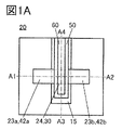
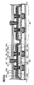
- FIG. 1A is a top view of a transistor that is one embodiment of the present invention.
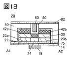
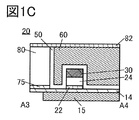
- 1B and 1C are cross-sectional views of transistors that are one embodiment of the present invention.
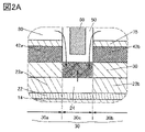
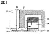
- 2A and 2B are cross-sectional views of a transistor that is one embodiment of the present invention.
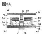
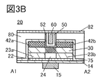
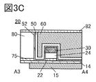
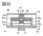
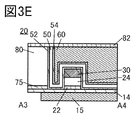
- 3A to 3E are cross-sectional views of transistors that are embodiments of the present invention.
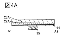
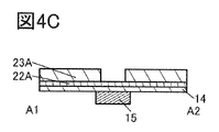
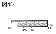
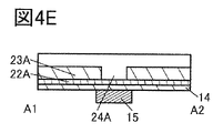
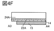
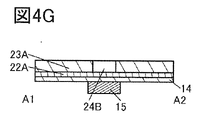
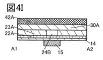
- 4A to 4J are cross-sectional views illustrating a method for manufacturing a transistor that is one embodiment of the present invention.
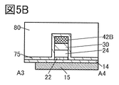
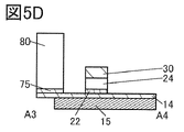
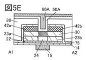
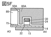
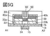
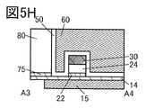
- 5A to 5H are cross-sectional views illustrating a method for manufacturing a transistor that is one embodiment of the present invention.
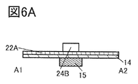
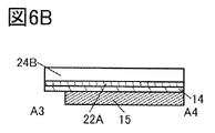
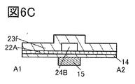
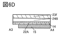
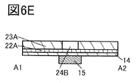
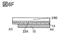
- 6A to 6F are cross-sectional views illustrating a method for manufacturing a transistor that is one embodiment of the present invention.
- FIG. 1A is a top view of a transistor that is one embodiment of the present invention.
- 1B and 1C are cross-sectional views of transistors that are one embodiment of the present invention.
- 2A and 2B are cross-section
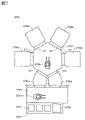
- FIG. 7 is a top view illustrating a microwave processing apparatus according to one aspect of the present invention.
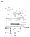
- FIG. 8 is a schematic cross-sectional view illustrating a microwave processing apparatus according to one aspect of the present invention.
- FIG. 9 is a cross-sectional schematic diagram illustrating a microwave processing apparatus according to one aspect of the present invention.
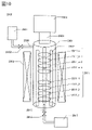
- FIG. 10 is a schematic diagram illustrating a microwave processing apparatus according to one aspect of the present invention.
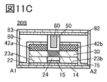
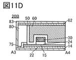
- 11A to 11D are cross-sectional views of transistors that are one embodiment of the present invention.
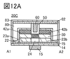
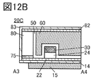
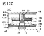
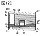
- 12A to 12D are cross-sectional views of transistors that are embodiments of the present invention.
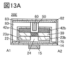
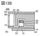
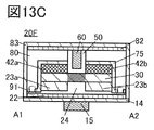
- 13A to 13D are cross-sectional views of transistors that are one embodiment of the present invention.
- FIG. 14A is a top view of a semiconductor device which is one embodiment of the present invention.
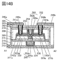
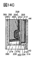
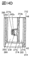
- 14B to 14D are cross-sectional views of semiconductor devices that are one embodiment of the present invention.
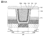
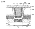
- 15A and 15B are cross-sectional views of a semiconductor device that is one embodiment of the present invention.
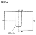
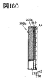
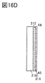
- FIG. 16A is a top view illustrating a method for manufacturing a semiconductor device which is one embodiment of the present invention.
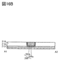
- 16B to 16D are cross-sectional views illustrating a method for manufacturing a semiconductor device which is one embodiment of the present invention.
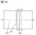
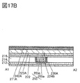
- FIG. 17A is a top view illustrating a method for manufacturing a semiconductor device which is one embodiment of the present invention.
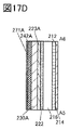
- 17B to 17D are cross-sectional views illustrating a method for manufacturing a semiconductor device which is one embodiment of the present invention.
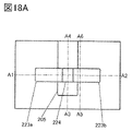
- 18A is a top view illustrating a method for manufacturing a semiconductor device which is one embodiment of the present invention.
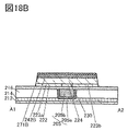
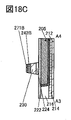
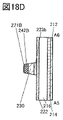
- 18B to 18D are cross-sectional views illustrating a method for manufacturing a semiconductor device which is one embodiment of the present invention.
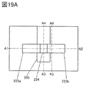
- FIG. 19A is a top view illustrating a method for manufacturing a semiconductor device which is one embodiment of the present invention.
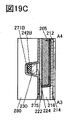
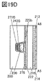
- 19B to 19D are cross-sectional views illustrating a method for manufacturing a semiconductor device which is one embodiment of the present invention.
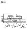
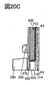
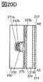
- FIG. 20A is a top view illustrating a method for manufacturing a semiconductor device which is one embodiment of the present invention.
- 20B to 20D are cross-sectional views illustrating a method for manufacturing a semiconductor device which is one embodiment of the present invention.
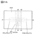
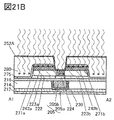
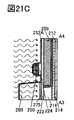
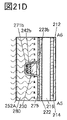
- 21A is a top view illustrating a method for manufacturing a semiconductor device which is one embodiment of the present invention.
- 21B to 21D are cross-sectional views illustrating a method for manufacturing a semiconductor device which is one embodiment of the present invention.
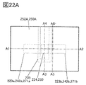
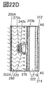
- FIG. 22A is a top view illustrating a method for manufacturing a semiconductor device which is one embodiment of the present invention.
- 22B to 22D are cross-sectional views illustrating a method for manufacturing a semiconductor device which is one embodiment of the present invention.
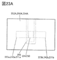
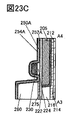
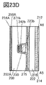
- FIG. 23A is a top view illustrating a method for manufacturing a semiconductor device which is one embodiment of the present invention.
- 23B to 23D are cross-sectional views illustrating a method for manufacturing a semiconductor device which is one embodiment of the present invention.
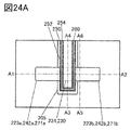
- 24A is a top view illustrating a method for manufacturing a semiconductor device which is one embodiment of the present invention.
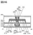
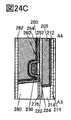
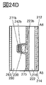
- 24B to 24D are cross-sectional views illustrating a method for manufacturing a semiconductor device which is one embodiment of the present invention.
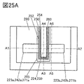
- FIG. 25A is a top view illustrating a method for manufacturing a semiconductor device which is one embodiment of the present invention.
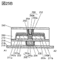
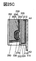
- 25B to 25D are cross-sectional views illustrating a method for manufacturing a semiconductor device which is one embodiment of the present invention.
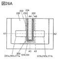
- FIG. 26A is a top view illustrating a method for manufacturing a semiconductor device which is one embodiment of the present invention.
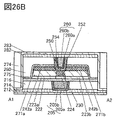
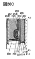
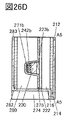
- 26B to 26D are cross-sectional views illustrating a method for manufacturing a semiconductor device which is one embodiment of the present invention.
- FIG. 27A is a top view illustrating a method for manufacturing a semiconductor device which is one embodiment of the present invention.
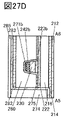
- 27B to 27D are cross-sectional views illustrating a method for manufacturing a semiconductor device which is one embodiment of the present invention.
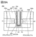
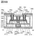
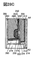
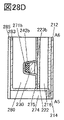
- FIG. 28A is a top view of a semiconductor device which is one embodiment of the present invention.
- 28B to 28D are cross-sectional views of semiconductor devices that are one embodiment of the present invention.
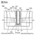
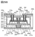
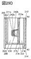
- FIG. 29A is a top view of a semiconductor device which is one embodiment of the present invention.
- 29B to 29D are cross-sectional views of semiconductor devices that are embodiments of the present invention.
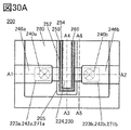
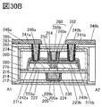
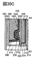
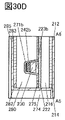
- FIG. 30A is a top view of a semiconductor device which is one embodiment of the present invention.
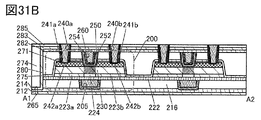
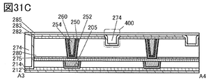
- FIG. 31A is a top view of a semiconductor device according to one embodiment of the present invention.
- 31B and 31C are cross-sectional views of a semiconductor device that is one embodiment of the present invention.
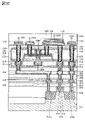
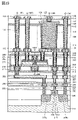
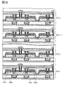
- FIG. 32 is a cross-sectional view illustrating a structure of a memory device according to one embodiment of the present invention.
- FIG. 33 is a cross-sectional view illustrating a structure of a memory device according to one embodiment of the present invention.
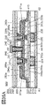
- FIG. 34 is a cross-sectional view of a semiconductor device according to one embodiment of the present invention.
- 35A and 35B are cross-sectional views of semiconductor devices according to one embodiment of the present invention.
- FIG. 36 is a cross-sectional view of a semiconductor device according to one embodiment of the present invention.
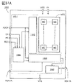
- FIG. 37A is a block diagram illustrating a configuration example of a memory device according to one embodiment of the present invention.
- FIG. 37B is a perspective view illustrating a configuration example of a memory device according to one embodiment of the present invention.
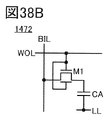
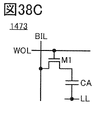
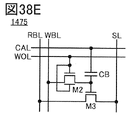
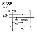
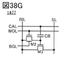
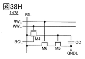
- 38A to 38H are circuit diagrams illustrating configuration examples of memory devices according to one embodiment of the present invention.
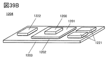
- 39A and 39B are schematic diagrams of a semiconductor device according to one embodiment of the present invention.
- FIG. 40 is a diagram illustrating a configuration example of a CPU.
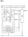
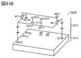
- 41A and 41B are diagrams illustrating configuration examples of a CPU.
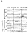
- FIG. 42 is a diagram showing the power gating sequence of the CPU.
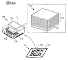
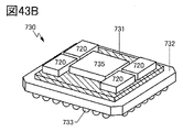
- 43A and 43B are diagrams illustrating an example of an electronic component.
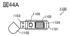
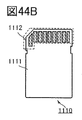
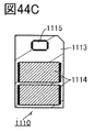
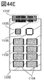
- 44A to 44E are schematic diagrams of a memory device according to one embodiment of the present invention.
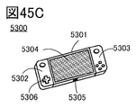
- 45A to 45H are diagrams illustrating
- top views also referred to as “plan views”
- perspective views also referred to as “plan views”
- description of some hidden lines may be omitted.
- the ordinal numbers such as first and second are used for convenience and do not indicate the order of steps or the order of stacking. Therefore, for example, “first” can be appropriately replaced with “second” or “third”. Also, the ordinal numbers described in this specification and the like may not match the ordinal numbers used to specify one aspect of the present invention.
- connection relationships other than the connection relationships shown in the drawings or the text are not limited to the predetermined connection relationships, for example, the connection relationships shown in the drawings or the text.
- X and Y are objects (for example, devices, elements, circuits, wiring, electrodes, terminals, conductive films, layers, etc.).
- a transistor is an element having at least three terminals including a gate, a drain, and a source.
- a region in which a channel is formed (hereinafter also referred to as a channel formation region) is provided between the drain (drain terminal, drain region, or drain electrode) and the source (source terminal, source region, or source electrode).
- a current can flow between the source and the drain through the formation region.
- a channel formation region means a region where current mainly flows.
- the function of the source or drain may be switched when using transistors of different polarities or when the direction of current changes in circuit operation. Therefore, in this specification and the like, the terms “source” and “drain” can be used interchangeably in some cases.
- the channel length is, for example, a region in which a semiconductor (or a portion of the semiconductor in which current flows when the transistor is on) overlaps with a gate electrode in a top view of a transistor, or the source length in a channel formation region.
- the channel length does not always have the same value in all regions of one transistor. That is, the channel length of one transistor may not be fixed to one value. Therefore, in this specification, the channel length is any one value, maximum value, minimum value, or average value in the channel forming region.
- the channel width is the region in which the semiconductor (or the portion of the semiconductor where current flows when the transistor is on) and the gate electrode overlap each other, or the channel length direction in the channel formation region.
- a channel width in a region where a channel is actually formed (hereinafter also referred to as an “effective channel width”) and a channel width shown in a top view of a transistor ( hereinafter also referred to as “apparent channel width”) may be different.
- the effective channel width becomes larger than the apparent channel width, and its influence cannot be ignored.
- the proportion of the channel formation region formed on the side surface of the semiconductor may be large. In that case, the effective channel width is larger than the apparent channel width.
- channel width may refer to the apparent channel width.
- channel width may refer to the effective channel width.
- the values of the channel length, channel width, effective channel width, apparent channel width, and the like can be determined, for example, by analyzing a cross-sectional TEM (Transmission Electron Microscope) image.
- impurities in a semiconductor refer to, for example, substances other than the main components that constitute the semiconductor.
- an element whose concentration is less than 0.1 atomic percent can be said to be an impurity.
- the inclusion of impurities may cause, for example, an increase in the defect level density of the semiconductor, a decrease in crystallinity, or the like.
- impurities that change the characteristics of the semiconductor include, for example, Group 1 elements, Group 2 elements, Group 13 elements, Group 14 elements, Group 15 elements, and oxide semiconductors.
- transition metals other than the main components of such as hydrogen, lithium, sodium, silicon, boron, phosphorus, carbon, and nitrogen.
- water may also function as an impurity.
- oxygen vacancies also referred to as V 2 O 3
- silicon oxynitride contains more oxygen than nitrogen as its composition.
- Silicon nitride oxide contains more nitrogen than oxygen in its composition.
- aluminum oxynitride has a higher content of oxygen than nitrogen as its composition.
- aluminum oxynitride has a composition in which the content of nitrogen is higher than that of oxygen.
- hafnium oxynitride has a higher content of oxygen than nitrogen as its composition.
- hafnium oxynitride has a composition in which the content of nitrogen is higher than that of oxygen.
- insulator can be replaced with an insulating film or an insulating layer.
- conductor can be replaced with a conductive film or a conductive layer.
- semiconductor can be interchanged with a semiconductor film or a semiconductor layer.
- parallel means a state in which two straight lines are arranged at an angle of -10 degrees or more and 10 degrees or less. Therefore, the case of ⁇ 5 degrees or more and 5 degrees or less is also included.
- substantially parallel means a state in which two straight lines are arranged at an angle of -30 degrees or more and 30 degrees or less.
- Perfect means that two straight lines are arranged at an angle of 80 degrees or more and 100 degrees or less. Therefore, the case of 85 degrees or more and 95 degrees or less is also included.
- substantially perpendicular means a state in which two straight lines are arranged at an angle of 60 degrees or more and 120 degrees or less.
- a metal oxide is a metal oxide in a broad sense.
- Metal oxides are classified into oxide insulators, oxide conductors (including transparent oxide conductors), oxide semiconductors (also referred to as oxide semiconductors or simply OSs), and the like.
- oxide semiconductors also referred to as oxide semiconductors or simply OSs
- an OS transistor can be referred to as a transistor including a metal oxide or an oxide semiconductor.
- the term “normally-off” means that the drain current per 1 ⁇ m of the channel width flowing through the transistor when no potential is applied to the gate or when a ground potential is applied to the gate is 1 ⁇ 10 ⁇ 1 at room temperature. 20 A or less, 1 ⁇ 10 ⁇ 18 A or less at 85° C., or 1 ⁇ 10 ⁇ 16 A or less at 125° C.
- Voltage is a potential difference from a reference potential.
- the reference potential is ground potential
- “voltage” can be replaced with “potential”. Note that the ground potential does not necessarily mean 0V.
- the potential is relative, and when the reference potential changes, the potential applied to the wiring, the potential applied to the circuit, etc., and the potential output from the circuit etc. also change.
- the heights are the same or approximately the same” refers to a configuration in which the heights from a reference surface (for example, a flat surface such as a substrate surface) are equal in cross-sectional view.
- planarization processing typically CMP processing
- CMP processing may expose the surface of a single layer or multiple layers.
- the surfaces to be CMP-processed have the same height from the reference surface.
- the heights of the layers may differ depending on the processing equipment, processing method, or material of the surface to be processed during the CMP processing. In this specification and the like, this case is also treated as "the height matches or roughly matches".
- the height of the top surface of the first layer and the height of the second layer A case where the height difference from the upper surface is 20 nm or less is also referred to as "matching or substantially matching heights".
- the ends match or roughly match means that at least part of the outline overlaps between the laminated layers when viewed from the top.
- the upper layer and the lower layer may be processed with the same mask pattern or partially with the same mask pattern.
- the contours do not overlap, and the upper contour may be positioned inside the lower contour, or the upper contour may be positioned outside the lower contour. “match or approximate match”.
- FIGS. 1A-1C are top and cross-sectional views of transistor 20.
- FIG. FIG. 1A is a top view of transistor 20.
- FIG. 1B and 1C are cross-sectional views of the transistor 20.
- FIG. 1B is a cross-sectional view of the portion indicated by the dashed-dotted line A1-A2 in FIG. 1A, and is also a cross-sectional view of the transistor 20 in the channel length direction.
- FIG. 1C is a cross-sectional view of the portion indicated by the dashed-dotted line A3-A4 in FIG. 1A, and is also a cross-sectional view of the channel forming region in the channel width direction of the transistor 20 and its vicinity. Note that some elements are omitted in the top view of FIG. 1A for clarity of illustration.
- the transistor 20 has a conductor 15 on a substrate (not shown), an insulator 14 on the conductor 15, an insulator 22 on the insulator 14, an insulator 24 on the insulator 22, and an insulator 23a on the insulator 22.
- the insulator 75 over the body 42a and the conductor 42b, the insulator 80 over the insulator 75, and the insulator 82 over the insulator 80, the insulator 50, and the conductor 60 are have.
- the insulator 23a and the insulator 23b may be collectively called the insulator 23.
- the conductor 42a and the conductor 42b may be collectively referred to as the conductor 42 in some cases.
- the insulator 80 and the insulator 75 are provided with openings reaching the oxide 30 .
- An insulator 50 and a conductor 60 are arranged in the opening.
- An insulator 50 and a conductor 60 are provided between the conductor 42 a and the conductor 42 b in the channel length direction of the transistor 20 .
- the insulator 50 has a region in contact with the side surface of the conductor 60 and a region in contact with the bottom surface of the conductor 60 .
- the insulator 50 includes a top surface of the insulator 14, a side surface of the insulator 22, a side surface of the insulator 24, a side surface of the oxide 30, a top surface of the oxide 30, a side surface of the conductor 42a, a side surface of the conductor 42b, and an insulating layer. It has regions in contact with the sides of the body 75 and the sides of the insulator 80 .
- the upper surface of the conductor 60 is arranged so that the top of the insulator 50 and the upper surface of the insulator 80 match or substantially match in height.
- the side surface of the opening in which the conductor 60 and the like are embedded is substantially perpendicular to the surface on which the oxide 30 is formed, but the present embodiment is not limited to this.
- the bottom of the opening may be U-shaped with a gently curved surface.
- the side surface of the opening may be inclined with respect to the surface on which the oxide 30 is formed.
- the top surface of the insulator 24 is arranged so that the top surface of the insulator 23a and the top surface of the insulator 23b match or substantially match in height.
- the conductor 60 functions as a first gate (also called top gate) electrode, and the conductor 15 functions as a second gate (also called back gate) electrode.
- insulator 50 functions as a first gate insulator, and insulators 22 and 24 function as second gate insulators. Note that the insulator 23 may function as a second gate insulator.
- the conductor 42a functions as one of the source electrode and the drain electrode, and the conductor 42b functions as the other of the source electrode and the drain electrode. At least part of the region of the oxide 30 overlapping with the conductor 60 functions as a channel formation region.
- the transistor 20 preferably uses a metal oxide functioning as a semiconductor (hereinafter also referred to as an oxide semiconductor) for the oxide 30 including the channel formation region.
- a metal oxide functioning as a semiconductor hereinafter also referred to as an oxide semiconductor
- the metal oxide that functions as a semiconductor preferably has a bandgap of 2 eV or more, more preferably 2.5 eV or more. By using a metal oxide with a large bandgap in this manner, off-state current of a transistor can be reduced.
- an In-M-Zn oxide containing indium, element M and zinc (element M is aluminum, gallium, yttrium, tin, copper, vanadium, beryllium, boron, titanium, iron, nickel, germanium , zirconium, molybdenum, lanthanum, cerium, neodymium, hafnium, tantalum, tungsten, or magnesium).
- element M is aluminum, gallium, yttrium, tin, copper, vanadium, beryllium, boron, titanium, iron, nickel, germanium , zirconium, molybdenum, lanthanum, cerium, neodymium, hafnium, tantalum, tungsten, or magnesium.
- element M is aluminum, gallium, yttrium, tin, copper, vanadium, beryllium, boron, titanium, iron, nickel, germanium , zirconium, molybdenum, lanthanum, cerium
- the oxide 30 preferably has crystallinity.
- CAAC-OS c-axis aligned crystal oxide semiconductor
- CAAC-OS is a metal oxide that has a dense structure with high crystallinity and few impurities or defects (eg, oxygen vacancies (VO), metal vacancies, and the like).
- impurities or defects eg, oxygen vacancies (VO), metal vacancies, and the like.
- heat treatment is performed at a temperature at which the metal oxide does not become polycrystalline (for example, 400° C. or higher and 600° C. or lower), so that the CAAC-OS has a dense structure with higher crystallinity. can be By increasing the density of the CAAC-OS in this manner, impurities or defects in the CAAC-OS can be further reduced.
- FIGS. 1B and 1C show a structure in which the oxide 30 is a single layer, the present invention is not limited to this, and a laminated structure of two or more layers may be used.
- regions 30a, 30b, and 30c which will be described later, may be formed in some of the layers or may be formed in all of the layers. good.
- the oxide 30 may have a laminated structure of multiple oxide layers with different chemical compositions.
- the atomic ratio of In to the element M is the atomic ratio of In to the element M in the metal oxide used for the oxide layer on the conductor 15 side. Larger is preferred. With this configuration, the transistor 20 can obtain a large on-current and high frequency characteristics.
- the plurality of oxide layers contain a common element other than oxygen as a main component, it is possible to reduce the defect level density at the interface of the oxide layers. Since the defect level density at the interface of the oxide layer can be reduced, the effect of interface scattering on carrier conduction is small, and a high on-current can be obtained.
- FIG. 2A shows an enlarged view of the channel forming region and its vicinity in FIG. 1B
- FIG. 2B shows an enlarged view of the channel forming region and its vicinity in FIG. 1C
- the oxide 30 has a region 30c and a pair of regions 30a and 30b provided to sandwich the region 30c. At least a portion of the region 30 c overlaps the conductor 60 .
- the region 30c is provided in the region between the conductors 42a and 42b.
- the region 30a is provided so as to overlap the conductor 42a
- the region 30b is provided so as to overlap the conductor 42b.
- the region 30c functions as a channel forming region of the transistor 20. Also, the region 30a functions as one of the source region and the drain region of the transistor 20, and the region 30b functions as the other of the source region and the drain region of the transistor 20.
- FIG. 1 A block diagram illustrating an exemplary transistor circuitry.
- the region 30c functioning as a channel forming region is a high-resistance region with a low carrier concentration because it has less oxygen vacancies or a lower concentration of impurities such as hydrogen, nitrogen, and metal elements than the regions 30a and 30b.
- the carrier concentration of the region 30c is preferably 1 ⁇ 10 18 cm ⁇ 3 or less, more preferably less than 1 ⁇ 10 17 cm ⁇ 3 , and less than 1 ⁇ 10 16 cm ⁇ 3 . It is more preferably less than 1 ⁇ 10 13 cm ⁇ 3 , even more preferably less than 1 ⁇ 10 12 cm ⁇ 3 .
- the lower limit of the carrier concentration of the region 30c it can be set to 1 ⁇ 10 ⁇ 9 cm ⁇ 3 , for example.
- the hydrogen concentration in the oxide 30 is less than 1 ⁇ 10 20 atoms/cm 3 , preferably It has a region of less than 1 ⁇ 10 19 atoms/cm 3 , more preferably less than 5 ⁇ 10 18 atoms/cm 3 , and even more preferably less than 1 ⁇ 10 18 atoms/cm 3 .
- said region is preferably located within region 30c of oxide 30 .
- the impurity concentration in the layer when the layer is measured by SIMS may be referred to as "the impurity concentration in the layer obtained by SIMS.”
- the regions 30a and 30b functioning as the source region or the drain region have many oxygen defects or have a high concentration of impurities such as hydrogen, nitrogen, and metal elements, so that the carrier concentration is increased and the resistance is lowered. That is, the regions 30a and 30b have a higher carrier concentration and a lower resistance than the region 30c.
- the carrier concentration of each of the regions 30a and 30b is preferably 1 ⁇ 10 17 cm ⁇ 3 or more, more preferably 1 ⁇ 10 18 cm ⁇ 3 or more, and 1 ⁇ 10 19 cm ⁇ 3 or more. is more preferable.
- the upper limit of the carrier concentration of each of the regions 30a and 30b it can be, for example, 1 ⁇ 10 21 cm ⁇ 3 .
- the carrier concentration is equal to or lower than that of the regions 30a and 30b and equal to or higher than that of the region 30c.
- regions may be formed. That is, the region functions as a junction region between the region 30c and the region 30a or the region 30b.
- the bonding region may have a hydrogen concentration equal to or lower than that of regions 30a and 30b and equal to or higher than that of region 30c.
- the bonding region may have oxygen vacancies equal to or less than those of the regions 30a and 30b and equal to or greater than those of the region 30c.
- concentrations of impurity elements such as metal elements, hydrogen, and nitrogen detected in each region are not limited to stepwise changes for each region, and may change continuously within each region. In other words, it is sufficient if the concentrations of impurity elements such as metal elements, hydrogen, and nitrogen decrease in regions closer to the channel formation region.
- a transistor including an oxide semiconductor tends to have electrical characteristics that fluctuate, and reliability may be degraded.
- hydrogen in the vicinity of oxygen vacancies may form defects in which hydrogen enters oxygen vacancies (hereinafter sometimes referred to as V OH ) to generate electrons serving as carriers. Therefore, if oxygen vacancies are included in the channel formation region in the oxide semiconductor, the transistor has normally-on characteristics (a channel exists even if no voltage is applied to the gate electrode, and a current flows through the transistor). easy to become. Therefore, impurities, oxygen vacancies, and VOH are preferably reduced as much as possible in the channel formation region in the oxide semiconductor.
- the channel formation region in the oxide semiconductor preferably has a reduced carrier concentration and is i-type (intrinsic) or substantially i-type.
- the source region and the drain region in the oxide semiconductor preferably have a high carrier concentration and are n-type. Therefore, the source region and the drain region in the oxide semiconductor preferably contain V OH that generates electrons serving as carriers. However, diffusion of VOH contained in the source and drain regions into the channel forming region must be suppressed. Therefore, it is preferable that the VOH contained in the source and drain regions is stable. In particular, variation in VOH contained in the source region and the drain region within the substrate surface causes variation in the electrical characteristics of the transistor.
- the region 30c functioning as a channel forming region preferably has a reduced carrier concentration and is i-type or substantially i-type.
- the regions 30a and 30b functioning as source regions or drain regions preferably have a high carrier concentration and are n-type.
- the i-type or substantially i-type region 30c and the n-type regions 30a and 30b are preferably stable.
- an insulator containing oxygen that is released by heating (hereinafter sometimes referred to as excess oxygen) is provided in the vicinity of the oxide semiconductor, and heat treatment is performed so that the oxide semiconductor is converted from the insulator.
- Oxygen can be supplied and oxygen vacancies and VOH can be reduced.
- the on current of the transistor 20 may decrease or the field effect mobility may decrease.
- variations in the amount of oxygen supplied to the source region or the drain region within the substrate plane cause variations in the electrical characteristics of the transistor.
- the region 30c functioning as a channel forming region preferably has a reduced carrier concentration and is i-type or substantially i-type.
- the region 30b has a high carrier concentration and is preferably n-type. That is, it is preferable to reduce oxygen vacancies and VOH in the region 30c of the oxide semiconductor and prevent excessive amounts of oxygen from being supplied to the regions 30a and 30b.
- an insulator containing excess oxygen is used as the insulator in contact with the top surface of the region 30c and the insulator in contact with the bottom surface of the region 30c.
- an insulator that suppresses diffusion of oxygen eg, at least one of oxygen atoms and oxygen molecules
- oxygen can be efficiently supplied to the region 30c, and the channel formation region can be a stable i-type region.
- the regions 30a and 30b are supplied with a smaller amount of oxygen than the region 30c, it is possible to prevent a decrease in carrier concentration in the source and drain regions.
- the insulator 50 is an insulator in contact with the top surface of the region 30c
- the insulator 24 is an insulator in contact with the bottom surface of the region 30c. Since the region 30c is provided so as to overlap the conductor 60, the insulator 24 overlaps the conductor 60 via the region 30c. In other words, insulator 24 is arranged to overlap oxide 30 and conductor 60 .
- the insulator 50 and the insulator 24 are preferably insulators containing excess oxygen. At this time, oxygen contained in the insulator 50 and the insulator 24 can be efficiently supplied to the region 30c.
- an insulator 80 is an insulator in contact with the insulator 50 .
- the insulator 80 is preferably an insulator containing excess oxygen.
- the insulator 24 may be formed using an insulating material that easily transmits oxygen. With this structure, oxygen contained in the insulator 80 can be supplied to the region 30 c through the insulators 50 and 24 .
- the arrows shown in FIG. 2A visualize how oxygen contained in the insulator 80 diffuses into the region 30c through the insulator 50 and how oxygen contained in the insulator 24 diffuses into the region 30c. be.
- the arrows shown in FIG. 2B show how oxygen contained in the insulator 80 diffuses into the region 30c through the insulator 50, and how oxygen contained in the insulator 80 diffuses through the insulator 50 and the insulator 24 into the region 30c. It visualizes how oxygen diffuses to 30c and how oxygen contained in the insulator 24 diffuses to region 30c.
- the insulator 50, the insulator 24, and the insulator 80 for example, silicon oxide, silicon oxynitride, silicon oxide to which fluorine is added, silicon oxide to which carbon is added, silicon oxide to which carbon and nitrogen are added, or holes are added.
- An insulating material such as silicon oxide can be used.
- silicon oxide and silicon oxynitride are preferable because they are stable against heat.
- the insulator 50, the insulator 24, and the insulator 80 are insulators containing at least oxygen and silicon.
- the insulating material is also a material with a low dielectric constant. Since the insulator 80 also functions as an interlayer film, parasitic capacitance generated between wirings can be reduced by forming the insulator 80 using the insulator material.
- the concentrations of impurities such as water and hydrogen in each of the insulator 50, the insulator 24, and the insulator 80 are reduced.
- At least one of the insulator 50, the insulator 24, and the insulator 80 has a hydrogen concentration of less than 2 ⁇ 10 20 atoms/cm 3 , preferably less than 1 ⁇ 10 20 atoms/cm 3 in the film obtained by SIMS. , more preferably less than 5 ⁇ 10 19 atoms/cm 3 , more preferably less than 1 ⁇ 10 19 atoms/cm 3 .
- the insulator 50 must be provided in an opening formed in the insulator 80 or the like together with the conductor 60 .
- the film thickness of the insulator 50 is thin.
- the thickness of the insulator 50 is preferably 0.5 nm or more and 20 nm or less, more preferably 1.0 nm or more and 15.0 nm or less.
- the insulator 50 may at least partially have a region with the film thickness as described above.
- FIGS. 1B and 1C show a configuration in which the insulator 50 is a single layer
- the present invention is not limited to this, and may have a laminated structure of two or more layers.
- the lower layer can be formed using an insulator that easily transmits oxygen
- the upper layer can be formed using an insulator that has a function of suppressing diffusion of oxygen. preferable.
- diffusion of oxygen contained in the lower layer to the conductor 60 can be suppressed. In other words, reduction in the amount of oxygen supplied to the oxide 30 can be suppressed.
- oxidation of the conductor 60 due to oxygen contained in the lower layer can be suppressed.
- the lower layer may be provided using a material that can be used for the insulator 50 described above, and the upper layer may use an insulator containing oxides of one or both of aluminum and hafnium.
- the insulator aluminum oxide, hafnium oxide, an oxide containing aluminum and hafnium (hafnium aluminate), an oxide containing hafnium and silicon (hafnium silicate), or the like can be used.
- hafnium oxide is used as the upper layer
- the upper layer is an insulator containing at least oxygen and hafnium.
- the insulator 23a is an insulator in contact with the lower surface of the region 30a. Since the region 30a is provided so as to overlap the conductor 42a, the insulator 23a overlaps the conductor 42a via the region 30a. In other words, the insulator 23a is arranged so as to overlap with the oxide 30 and the conductor 42a. Insulator 23b is an insulator in contact with the lower surface of region 30b. Since the region 30b is provided so as to overlap the conductor 42b, the insulator 23b overlaps the conductor 42b via the region 30b. In other words, the insulator 23b is arranged so as to overlap with the oxide 30 and the conductor 42b.
- the insulators 23a and 23b preferably have a function of suppressing diffusion of oxygen.
- insulators having a function of suppressing diffusion of oxygen include aluminum oxide, magnesium oxide, hafnium oxide, oxides containing hafnium and silicon, oxides containing hafnium and aluminum, oxides containing hafnium and zirconium, and gallium oxide. , an oxide containing gallium and zinc, an In—Ga—Zn oxide, silicon nitride, silicon nitride oxide, or the like can be used.
- the insulators 23a and 23b only need to have a function of suppressing the diffusion of oxygen, and the insulators 23a and 23b are not limited to insulating materials, and semiconductor materials may be used.
- the insulators 23 a and 23 b preferably have compressive stress, and more preferably have a greater compressive stress than the oxide 30 .
- silicon nitride which can be applied to insulators 23 a and 23 b , has a higher compressive stress than oxide 30 .
- an insulator having a compressive stress particularly an insulator having a compressive stress greater than that of the oxide 30 is used. strain) can be formed. By stably forming VOH by tensile strain, the regions 30a and 30b can be made into stable n-type regions.
- the compressive stress of the insulator is the stress that tends to relax the compressed shape of the insulator, and is the stress that has a vector in the direction from the center to the end of the insulator.
- the In--Ga--Zn oxide is a metal oxide that can also be applied to the oxide 30.
- the on-state current and field-effect mobility of the transistor tend to increase as the atomic ratio of indium to gallium increases.
- diffusion of oxygen tends to be more suppressed as the atomic ratio of gallium to indium increases.
- the atomic ratio of indium to gallium in the In--Ga--Zn oxide used for the oxide 30 is It is preferably larger than the atomic number ratio of indium to gallium in the In--Ga--Zn oxide used for 23a and insulator 23b.
- the atomic ratio of gallium to indium in the In—Ga—Zn oxide used for the insulators 23 a and 23 b is the atomic ratio of gallium to indium in the In—Ga—Zn oxide used for the oxide 30 . Larger is preferred.
- the neighboring composition includes a range of ⁇ 30% of the desired atomic number ratio.
- the element M it is preferable to use gallium.
- the above atomic ratio is not limited to the atomic ratio of the deposited metal oxide, and the atomic ratio of the sputtering target used for the deposition of the metal oxide. may be
- the end portion of the insulator 23a on the conductor 60 side and the end portion of the region 30a on the conductor 60 side are aligned or substantially aligned, and the end portion of the insulator 23b on the conductor 60 side and the region 30b are aligned.
- the present invention is not limited to this.
- One or both of insulator 23a and insulator 23b may have a region that overlaps region 30c.
- FIG. 3A is a cross-sectional view of the transistor 20 in the channel length direction. Note that the cross-sectional structure of the transistor 20 shown in FIG. 3A in the channel width direction can be the same as the cross-sectional structure of the transistor 20 shown in FIG. 1C.
- the insulators 23a and 23b may have regions that overlap with the channel forming region of the oxide 30.
- the width of the insulator 24 is narrower than the width of the channel formation region in the channel length direction of the transistor 20 .
- Oxygen supplied to the CAAC-OS tends to diffuse in a direction perpendicular to the c-axis. Therefore, when CAAC-OS is used as the oxide 30, it is presumed that this structure can prevent an excessive amount of oxygen from being supplied to the source region and the drain region.
- An insulator to which oxygen can be added to the insulator 80 is preferably used as the insulator 82 .
- the insulator 82 becomes an insulator containing at least oxygen and aluminum.
- the insulator 82 or the insulating film to be the insulator 82 is preferably formed by a sputtering method, and more preferably by a sputtering method in an oxygen-containing atmosphere. By forming the insulator 82 or an insulating film to be the insulator 82 in an atmosphere containing oxygen by a sputtering method, oxygen can be added to the insulator 80 while the insulator 82 is being formed. This allows the insulator 80 to contain excess oxygen.
- a metal oxide having an amorphous structure as the insulator 82 .
- metal oxides such as aluminum oxide or magnesium oxide.
- a metal oxide having an amorphous structure has oxygen atoms with dangling bonds and may have the property of capturing or fixing hydrogen with the dangling bonds.
- hydrogen contained in the transistor 20 or hydrogen existing around the transistor 20 is captured or fixed. be able to.
- the transistor 20 with favorable characteristics and high reliability can be manufactured.
- the insulator 82 preferably has an amorphous structure, but may partially have a polycrystalline structure region.
- the insulator 82 may have a multi-layer structure in which a layer having an amorphous structure and a layer having a polycrystalline structure are laminated.
- a laminated structure in which a layer of polycrystalline structure is formed on a layer of amorphous structure may be used.
- the insulator 75 is, as shown in FIG. 1B, configured to be in contact with part of the upper surface of the insulator 14 .
- Oxide 30 is thus located within the region encapsulated by insulator 75 and insulator 14 .
- the insulator 75 and the insulator 14 preferably function as a barrier insulating film that suppresses diffusion of impurities such as water and hydrogen into the sealed region. Therefore, for the insulator 14 and the insulator 75, it is preferable to use an insulating material that has a function of suppressing diffusion of impurities such as hydrogen atoms, hydrogen molecules, and water molecules (that is, the impurities hardly permeate). With this structure, impurities such as water and hydrogen contained outside the sealed region can be prevented from entering the sealed region. Therefore, impurities such as water and hydrogen can be prevented from entering the oxide 30 .
- a barrier insulating film refers to an insulating film having barrier properties.
- barrier property refers to the function of suppressing the diffusion of the corresponding substance (also referred to as “low permeability”).
- the corresponding substance has the function of capturing and fixing (also called gettering).
- an insulator having a function of suppressing diffusion of impurities such as water and hydrogen is preferably used. Any one or a plurality of materials selected from oxides containing zinc, In—Ga—Zn oxides, silicon nitride, and silicon oxynitride can be used.
- silicon nitride which has a higher hydrogen barrier property, is preferably used for the insulator 14 and the insulator 75 .
- the insulator 14 and the insulator 75 are insulators containing at least nitrogen and silicon. Note that each of the insulator 14 and the insulator 75 may have a laminated structure (a laminated structure of two or more layers) in which the above materials are combined.
- the insulator 22 it is preferable to select an insulator that functions as an etching stopper film when trenches are formed by etching the insulating film that will become the insulators 23a and 23b.
- the insulator 22 may be made of aluminum oxide, In--Ga--Zn oxide, or the like. As described above, the material used for the insulator 22 may be appropriately selected according to the material used for the insulating film forming the groove.
- the insulator 22 may use a metal oxide having an amorphous structure.
- a metal oxide that can be used for the insulator 82 is preferably used as the insulator 22 . With this structure, hydrogen contained in the channel formation region of the transistor 20 and diffused into the insulator 22 through the insulator 24 can be captured or fixed.
- the conductor 60 is formed in a self-aligned manner so as to fill an opening formed in the insulator 80 or the like. By forming the conductor 60 in this manner, the conductor 60 can be reliably arranged in the region between the conductors 42a and 42b without being aligned.
- the conductor 60 also functions as wiring, it is preferable to use a conductor with high conductivity.
- the conductor 60 can use a conductive material whose main component is tungsten, copper, or aluminum.
- 1B and 1C show the conductor 60 as having a single-layer structure, but may have a laminated structure of two or more layers.
- the layer on the insulator 50 side suppresses diffusion of impurities such as hydrogen atoms, hydrogen molecules, water molecules, nitrogen atoms, nitrogen molecules, nitrogen oxide molecules, and copper atoms. It is preferable to use a conductive material having a function. Alternatively, a conductive material having a function of suppressing diffusion of oxygen (eg, at least one of oxygen atoms and oxygen molecules) is preferably used.
- the layer on the insulator 50 side has a function of suppressing the diffusion of oxygen
- the oxygen contained in the insulator 50 oxidizes the layers arranged inside the layer on the insulator 50 side, thereby reducing the conductivity.
- the conductive material having a function of suppressing diffusion of oxygen titanium, titanium nitride, tantalum, tantalum nitride, ruthenium, ruthenium oxide, or the like is preferably used, for example.
- the height of the bottom surface of the region of the conductor 60 where the conductor 60 and the oxide 30 do not overlap with the bottom surface of the insulator 14 in the channel width direction of the transistor 20 is measured.
- the height is preferably less than the height of the bottom surface of oxide 30 .
- the conductor 60 functioning as a gate electrode covers the side surface and the top surface of the channel formation region of the oxide 30 with the insulator 50 interposed therebetween. It becomes easier to act on Therefore, it is possible to increase the ON current of the transistor 20 and improve the frequency characteristic.
- the difference between the height of the bottom surface of the conductor 60 and the height of the bottom surface of the oxide 30 in a region where the oxide 30 and the conductor 60 do not overlap with respect to the bottom surface of the insulator 14 is 0 nm. 100 nm or less, preferably 3 nm or more and 50 nm or less, more preferably 5 nm or more and 20 nm or less.
- the conductors 42 a and 42 b are provided in contact with the upper surface of the oxide 30 .
- the conductor 42 may be, for example, a nitride containing tantalum, a nitride containing titanium, a nitride containing molybdenum, a nitride containing tungsten, a nitride containing tantalum and aluminum, or a nitride containing titanium and aluminum. It is preferable to use any one or more selected from among them. In one aspect of the present invention, nitrides containing tantalum are particularly preferred. Alternatively, for example, ruthenium oxide, ruthenium nitride, an oxide containing strontium and ruthenium, an oxide containing lanthanum and nickel, or the like may be used. These materials are preferable because they are conductive materials that are difficult to oxidize or materials that maintain conductivity even after absorbing oxygen.
- FIG. 1B shows a configuration in which the conductor 42 is provided as a single layer
- the conductor 42 may be provided as a laminated structure of two or more layers. At this time, it is preferable to stack a plurality of conductive layers formed using any of the above materials. Alternatively, a plurality of conductive layers formed using any of the above materials may be stacked with different compositions.
- a laminated structure of a nitride containing tantalum and a nitride containing titanium on the nitride containing tantalum can be preferably used.
- hydrogen contained in the oxide 30 or the like may diffuse into the conductor 42a or the conductor 42b.
- hydrogen contained in the oxide 30 or the like easily diffuses into the conductor 42a or the conductor 42b, and the diffused hydrogen It may bond with nitrogen contained in 42a or conductor 42b. That is, hydrogen contained in the oxide 30 or the like might be absorbed by the conductor 42a or the conductor 42b.
- the sheet resistance of the oxide 30 in the region overlapping with the conductor 42a (the conductor 42b) is reduced.
- the carrier concentration may increase. Therefore, the resistance of the oxide 30 in the region overlapping with the conductor 42a (conductor 42b) can be reduced in a self-aligning manner.
- microwave treatment it is preferable to perform microwave treatment in an atmosphere containing oxygen with the conductor 42a and the conductor 42b provided over the oxide 30 .
- the microwave treatment refers to treatment using an apparatus having a power supply for generating high-density plasma using microwaves, for example.
- microwaves refer to electromagnetic waves having a frequency of 300 MHz or more and 300 GHz or less.
- oxygen gas By performing microwave treatment in an atmosphere containing oxygen, oxygen gas can be converted into plasma using microwaves or high frequencies such as RF, and the oxygen plasma can act. At this time, the region 30c can also be irradiated with microwaves or high frequencies such as RF.
- V OH in the region 30c can be divided into oxygen vacancies and hydrogen, the hydrogen can be removed from the region 30c, and the oxygen vacancies can be filled with oxygen. Therefore, the hydrogen concentration, oxygen deficiency, and VOH in the region 30c can be reduced, and the carrier concentration can be lowered. Also, by preventing an excessive amount of oxygen from being introduced into the chamber in the microwave treatment, it is possible to prevent the carrier concentration from excessively decreasing in the regions 30a and 30b.
- the insulating film to be the insulator 50 it is preferable to perform microwave treatment in an atmosphere containing oxygen.
- oxygen can be efficiently injected into the region 30c.
- the oxygen injected into the region 30c has various forms such as oxygen atoms, oxygen molecules, and oxygen radicals (also called O radicals, atoms, molecules, or ions having unpaired electrons).
- the oxygen injected into the region 30c may be one or more of the forms described above, and oxygen radicals are particularly preferable.
- the film quality of the insulator 50 can be improved, the reliability of the transistor 20 is improved.
- oxygen vacancies and VOH can be selectively removed from the oxide semiconductor region 30c to make the region 30c i-type or substantially i-type. Furthermore, excessive supply of oxygen to the regions 30a and 30b functioning as the source region or the drain region can be suppressed, and the state of the n-type region before the microwave treatment can be maintained. As a result, variations in the electrical characteristics of the transistor 20 can be suppressed, and variation in the electrical characteristics of the transistor 20 within the substrate surface can be suppressed.
- the conductor 15 is arranged so as to overlap with the oxide 30 and the conductor 60 .
- the conductor 15 is preferably provided larger than the area of the oxide 30 that does not overlap the conductors 42a and 42b.
- the conductor 15 preferably extends also in a region outside the edge of the oxide 30 in the channel width direction. In other words, it is preferable that the conductor 15 and the conductor 60 overlap each other with an insulator interposed therebetween on the outside of the side surface of the oxide 30 in the channel width direction.
- the electric field of the conductor 60 functioning as the first gate electrode and the electric field of the conductor 15 functioning as the second gate electrode electrically surround the channel formation region of the oxide 30 . can be done.
- a transistor structure in which a channel formation region is electrically surrounded by electric fields of a first gate and a second gate is referred to as a surrounded channel (S-channel) structure.
- a transistor with an S-channel structure represents a transistor structure in which a channel formation region is electrically surrounded by electric fields of one and the other of a pair of gate electrodes.
- the S-channel structure disclosed in this specification and the like is different from the Fin type structure and the planar type structure.
- the transistor can have increased resistance to the short channel effect, in other words, a transistor in which the short channel effect is less likely to occur.
- the transistor 20 By setting the transistor 20 to be normally off and having the above S-channel structure, the channel formation region can be electrically surrounded. Therefore, the transistor 20 can also be regarded as having a GAA (Gate All Around) structure or an LGAA (Lateral Gate All Around) structure.
- GAA Gate All Around
- LGAA LayerAA
- the S-channel structure, the GAA structure, or the LGAA structure for the transistor 20 the entire bulk of the oxide 30 is used as the channel formation region formed at or near the interface between the oxide 30 and the gate insulator. can be done. Therefore, since the density of the current flowing through the transistor can be increased, it can be expected that the on-state current of the transistor or the field-effect mobility of the transistor can be increased.
- the conductor 15 is extended to function as wiring.
- a configuration in which a conductor functioning as wiring may be provided under the conductor 15 may be employed.
- one conductor 15 does not necessarily have to be provided for each transistor.
- the conductor 15 may be shared by a plurality of transistors.
- FIG. 1B shows a configuration in which the conductor 15 is provided as a single layer, the present invention is not limited to this.
- the conductor 15 may be provided as a laminated structure of two or more layers.
- the conductor 15 may function as a second gate electrode.
- the threshold voltage (Vth) of the transistor 20 can be controlled by changing the potential applied to the conductor 15 independently of the potential applied to the conductor 60 .
- the Vth of the transistor 20 can be increased and the off current can be reduced. Therefore, applying a negative potential to the conductor 15 can make the drain current smaller when the potential applied to the conductor 60 is 0V than in the case of not applying a negative potential.
- the electrical resistivity of the conductor 15 is designed in consideration of the potential applied to the conductor 15, and the film thickness of the conductor 15 is set according to the electrical resistivity.
- the conductor 15 may not be provided when the transistor 20 has normally-off characteristics or when the off-state current of the transistor 20 is small. By using a structure in which the conductor 15 is not provided, a manufacturing process of the transistor can be simplified and productivity can be improved.
- FIG. 1B shows a configuration in which the insulator 80 and the insulator 50 are in contact with each other
- the present invention is not limited to this.
- an insulator may be provided between the insulator 80 and the insulator 50 .
- FIGS. 3B and 3C are cross-sectional views of transistor 20.
- FIG. 3B is a cross-sectional view of the transistor 20 in the channel length direction
- FIG. 3C is a cross-sectional view of the transistor 20 in the channel width direction.
- the transistor 20 shown in FIGS. 3B and 3C has an insulator 52 over the oxide 30 . Also, the insulator 50 is provided on the insulator 52 . Also, the insulator 52 is provided between the insulator 80 and the insulator 50 .
- the insulator 52 is placed in the openings provided in the insulator 80 and the insulator 75 and covers the top surface of the insulator 14 , the side surfaces of the insulator 22 , the side surfaces of the insulator 24 , the side surfaces of the oxide 30 , and the oxide 30 . It is in contact with the upper surface, the side surface of the conductor 42a, the side surface of the conductor 42b, the side surface of the insulator 75, and the side surface of the insulator 80, respectively.
- An insulator 50 is arranged in the opening via an insulator 52 .
- the conductor 60 is arranged to fill the opening through the insulator 52 and the insulator 50 .
- the top surface of conductor 60 is arranged to be flush or nearly flush with the top surface of insulator 80 , the top of insulator 52 , and the top of insulator 50 .
- a part of the insulator 52 functions as a first gate insulator.
- the insulator 52 it is preferable to use a barrier insulating film against oxygen.
- an insulator that can be used for the insulator 82 described above may be used.
- an insulator containing oxides of one or both of aluminum and hafnium may be used.
- aluminum oxide, hafnium oxide, an oxide containing aluminum and hafnium (hafnium aluminate), an oxide containing hafnium and silicon (hafnium silicate), or the like can be used.
- aluminum oxide is used as the insulator 52 .
- the insulator 52 becomes an insulator containing at least oxygen and aluminum.
- Insulator 52 is provided in contact with the top and side surfaces of oxide 30 , the side surfaces of insulator 24 , the side surfaces of insulator 22 , and the top surface of insulator 14 . That is, the regions of the oxide 30 and the insulator 24 overlapping the conductor 60 are covered with the insulator 52 in the cross section in the channel width direction.
- the insulator 52 having a barrier property against oxygen can block the release of oxygen from the oxide 30 when heat treatment or the like is performed. Therefore, formation of oxygen vacancies in the oxide 30 can be reduced. As a result, oxygen vacancies and VOH formed in the region 30c can be reduced. Therefore, the electrical characteristics of the transistor 20 can be improved, and the reliability can be improved.
- the insulator 80, the insulator 50, the insulator 24, and the like contain an excessive amount of oxygen, excessive supply of the oxygen to the oxide 30 can be suppressed. Therefore, excessive oxidation of the regions 30a and 30b through the region 30c can be suppressed from causing a decrease in the ON current of the transistor 20 or a decrease in the field effect mobility.
- the insulator 52 is provided in contact with the side surfaces of the conductor 42, the insulator 75, and the insulator 80, respectively. Therefore, it is possible to prevent the side surfaces of the conductor 42 from being oxidized and forming an oxide film on the side surfaces. As a result, it is possible to suppress a decrease in the ON current of the transistor 20 or a decrease in the field effect mobility.
- the insulator 52 along with the insulator 50 and the conductor 60, must be provided in an opening formed in the insulator 80 or the like.
- the film thickness of the insulator 52 is thin.
- the thickness of the insulator 52 is 0.1 nm to 5.0 nm, preferably 0.5 nm to 3.0 nm, more preferably 1.0 nm to 3.0 nm.
- the insulator 52 may at least partially have a region having the film thickness as described above.
- the thickness of the insulator 52 is preferably thinner than the thickness of the insulator 50 . In this case, the insulator 52 may at least partially have a region thinner than the insulator 50 .
- the ALD method includes a thermal ALD (thermal ALD) method in which a precursor and a reactant react with only thermal energy, a PEALD (plasma enhanced ALD) method using a plasma-excited reactant, and the like.
- thermal ALD thermal ALD
- PEALD plasma enhanced ALD
- film formation can be performed at a lower temperature by using plasma, which is preferable in some cases.
- the ALD method can deposit atoms one layer at a time, it is possible to form extremely thin films, to form structures with a high aspect ratio, to form films with few defects such as pinholes, and to improve coverage. There are effects such as excellent film formation and low temperature film formation. Therefore, the insulator 52 can be formed with a thin film thickness as described above with good coverage on the side surfaces of the opening formed in the insulator 80 or the like.
- a film formed by the ALD method may contain more impurities such as carbon than films formed by other film formation methods.
- quantification of impurities can be performed using SIMS, X-ray Photoelectron Spectroscopy (XPS), or Auger Electron Spectroscopy (AES).
- the insulator 52 it is preferable to perform microwave treatment in the above-described atmosphere containing oxygen after forming the insulating film to be the insulator 52 .
- oxygen can be efficiently injected into the region 30c.
- the insulator 52 so as to be in contact with the side surface of the conductor 42 and the surface of the region 30c, it is possible to suppress the injection of more than a necessary amount of oxygen into the region 30c and suppress the oxidation of the side surface of the conductor 42. .
- oxidation of the side surface of the conductor 42 can be suppressed when the insulating film to be the insulator 50 is formed.
- the film quality of the insulator 52 can be improved, the reliability of the transistor 20 is improved.
- the microwave treatment may or may not be performed after the insulating film to be the insulator 50 is formed. Further, when the microwave treatment is performed after the insulating film to be the insulator 50 is formed, the microwave treatment may or may not be performed after the insulating film to be the insulator 52 is formed.
- FIGS. 3B and 3C show a configuration in which the insulator 50 and the conductor 60 are in contact with each other, the present invention is not limited to this.
- an insulator may be provided between the insulator 50 and the conductor 60 .
- FIGS. 3D and 3E are cross-sectional views of transistor 20.
- FIG. 3D is a cross-sectional view of the transistor 20 in the channel length direction
- FIG. 3E is a cross-sectional view of the transistor 20 in the channel width direction.
- the transistor 20 shown in FIGS. 3D and 3E has an insulator 54 on the insulator 50 . Also, the conductor 60 is provided on the insulator 54 . Also, the insulator 52 is provided between the insulator 50 and the conductor 60 .
- the insulator 54 is arranged in openings provided in the insulator 80 and the insulator 75 and is in contact with the insulator 50 and the conductor 60 .
- An insulator 54 is arranged in the opening via the insulators 50 and 52 .
- the conductor 60 is arranged to fill the opening with the insulator 54 , the insulator 50 , and the insulator 52 interposed therebetween.
- the top surface of conductor 60 is positioned to be flush or nearly flush with the top surface of insulator 80 , the top of insulator 52 , the top of insulator 50 , and the top of insulator 54 .
- a part of the insulator 54 functions as a first gate insulator.
- the insulator 54 it is preferable to use a barrier insulating film against hydrogen and water molecules. This can prevent impurities such as hydrogen contained in the conductor 60 from diffusing into the insulator 50 and the oxide 30 .
- an insulator that can be used for the insulator 14 described above may be used.
- silicon nitride deposited by the PEALD method may be used as the insulator 54 . In this case, the insulator 54 becomes an insulator containing at least nitrogen and silicon.
- the insulator 54 may further have a barrier property against oxygen. Thereby, diffusion of oxygen contained in the insulator 50 to the conductor 60 can be suppressed.
- the insulator 54 along with the insulator 52, the insulator 50, and the conductor 60, must be provided in openings formed in the insulator 80 or the like.
- the film thickness of the insulator 54 is thin.
- the thickness of the insulator 54 is 0.1 nm to 5.0 nm, preferably 0.5 nm to 3.0 nm, more preferably 1.0 nm to 3.0 nm.
- the insulator 54 may at least partially have a region with the film thickness as described above.
- the thickness of the insulator 54 is preferably thinner than the thickness of the insulator 50 . In this case, the insulator 54 may at least partially have a region thinner than the insulator 50 .
- an insulator substrate As the substrate on which the transistor 20 is formed, for example, an insulator substrate, a semiconductor substrate, or a conductor substrate may be used.
- insulator substrates include glass substrates, quartz substrates, sapphire substrates, stabilized zirconia substrates (yttria stabilized zirconia substrates, etc.), and resin substrates.
- Semiconductor substrates include, for example, semiconductor substrates made of silicon or germanium, or compound semiconductor substrates made of silicon carbide, silicon germanium, gallium arsenide, indium phosphide, zinc oxide, or gallium oxide. Further, there is a semiconductor substrate having an insulator region inside the semiconductor substrate, such as an SOI (Silicon On Insulator) substrate.
- SOI Silicon On Insulator
- Examples of conductive substrates include graphite substrates, metal substrates, alloy substrates, and conductive resin substrates. Alternatively, there are a substrate having a metal nitride, a substrate having a metal oxide, and the like. Furthermore, there are substrates in which an insulator substrate is provided with a conductor or a semiconductor, a substrate in which a semiconductor substrate is provided with a conductor or an insulator, a substrate in which a conductor substrate is provided with a semiconductor or an insulator, and the like. Alternatively, these substrates provided with elements may be used. Elements provided on the substrate include a capacitor element, a resistance element, a switch element, a light emitting element, a memory element, and the like.
- Insulators with a high relative dielectric constant include gallium oxide, hafnium oxide, zirconium oxide, oxides containing aluminum and hafnium, oxynitrides containing aluminum and hafnium, oxides containing silicon and hafnium, and silicon and hafnium. oxynitrides with silicon, or nitrides with silicon and hafnium.
- Insulators with a low relative dielectric constant include silicon oxide, silicon oxynitride, silicon nitride oxide, silicon nitride, silicon oxide to which fluorine is added, silicon oxide to which carbon is added, silicon oxide to which carbon and nitrogen are added, and an empty silicon oxide. There are silicon oxide with pores, resin, and the like.
- insulators having a function of suppressing permeation of impurities such as hydrogen and oxygen include boron, carbon, nitrogen, oxygen, fluorine, magnesium, aluminum, silicon, phosphorus, chlorine, argon, gallium, germanium, yttrium, and zirconium. Insulators including lanthanum, neodymium, hafnium, or tantalum may be used in single layers or in stacks.
- insulators having a function of suppressing permeation of impurities such as hydrogen and oxygen
- Metal oxides such as tantalum oxide, and metal nitrides such as aluminum nitride, silicon nitride oxide, and silicon nitride can be used.
- An insulator that functions as a gate insulator preferably has a region containing oxygen that is released by heating. For example, by forming a structure in which silicon oxide or silicon oxynitride having a region containing oxygen released by heating is in contact with the oxide 30, oxygen vacancies in the oxide 30 can be compensated.
- Conductors include aluminum, chromium, copper, silver, gold, platinum, tantalum, nickel, titanium, molybdenum, tungsten, hafnium, vanadium, niobium, manganese, magnesium, zirconium, beryllium, indium, ruthenium, iridium, strontium, and lanthanum. It is preferable to use a metal element selected from among the above, an alloy containing the above-described metal elements as a component, or an alloy or the like in which the above-described metal elements are combined.
- tantalum nitride, titanium nitride, tungsten, nitride containing titanium and aluminum, nitride containing tantalum and aluminum, ruthenium oxide, ruthenium nitride, oxide containing strontium and ruthenium, oxide containing lanthanum and nickel, and the like are used. is preferred. Also, tantalum nitride, titanium nitride, nitrides containing titanium and aluminum, nitrides containing tantalum and aluminum, ruthenium oxide, ruthenium nitride, oxides containing strontium and ruthenium, and oxides containing lanthanum and nickel are difficult to oxidize.
- a conductive material or a material that maintains conductivity even after absorbing oxygen.
- a semiconductor with high electrical conductivity typified by polycrystalline silicon containing an impurity element such as phosphorus, or a silicide such as nickel silicide may be used.
- a plurality of conductive layers formed of the above materials may be laminated and used.
- a laminated structure in which the material containing the metal element described above and the conductive material containing oxygen are combined may be used.
- a laminated structure may be employed in which the material containing the metal element described above and the conductive material containing nitrogen are combined.
- a laminated structure may be employed in which the material containing the metal element described above, the conductive material containing oxygen, and the conductive material containing nitrogen are combined.
- a stacked-layer structure in which the above-described material containing the metal element and a conductive material containing oxygen are combined is used for a conductor functioning as a gate electrode.
- a conductive material containing oxygen is preferably provided on the channel formation region side.
- a conductor functioning as a gate electrode it is preferable to use a conductive material containing oxygen and a metal element contained in a metal oxide in which a channel is formed.
- a conductive material containing the metal element and nitrogen described above may be used.
- a conductive material containing nitrogen such as titanium nitride or tantalum nitride may be used.
- indium tin oxide, indium oxide containing tungsten oxide, indium zinc oxide containing tungsten oxide, indium oxide containing titanium oxide, indium tin oxide containing titanium oxide, indium zinc oxide, and silicon were added.
- Indium tin oxide may also be used.
- indium gallium zinc oxide containing nitrogen may be used.
- a metal oxide (oxide semiconductor) that functions as a semiconductor is preferably used as the oxide 30 .
- Metal oxides applicable to the oxide 30 according to the present invention are described below.
- the metal oxide preferably contains at least indium or zinc. In particular, it preferably contains indium and zinc. In addition to these, it is preferable that aluminum, gallium, yttrium, tin, and the like are contained. Further, one or more selected from boron, titanium, iron, nickel, germanium, zirconium, molybdenum, lanthanum, cerium, neodymium, hafnium, tantalum, tungsten, magnesium, cobalt, etc. may be contained.
- the metal oxide is an In-M-Zn oxide having indium, the element M and zinc.
- the element M is aluminum, gallium, yttrium, or tin.
- Other elements applicable to element M include boron, titanium, iron, nickel, germanium, zirconium, molybdenum, lanthanum, cerium, neodymium, hafnium, tantalum, tungsten, magnesium, and cobalt.
- the element M there are cases where a plurality of the above elements may be combined.
- the element M is preferably one or more selected from gallium, aluminum, yttrium, and tin.
- an oxide containing indium (In), gallium (Ga), and zinc (Zn) (also referred to as IGZO) is preferably used for a semiconductor layer of a transistor.
- an oxide containing indium (In), aluminum (Al), and zinc (Zn) (also referred to as IAZO) may be used for the semiconductor layer of the transistor.
- an oxide containing indium (In), aluminum (Al), gallium (Ga), and zinc (Zn) (IAGZO) may be used for the semiconductor layer of the transistor.
- nitrogen-containing metal oxides may also be collectively referred to as metal oxides.
- a metal oxide containing nitrogen may also be referred to as a metal oxynitride.
- oxides containing indium (In), gallium (Ga), and zinc (Zn) will be described as examples of metal oxides. Note that an oxide containing indium (In), gallium (Ga), and zinc (Zn) is sometimes called an In--Ga--Zn oxide.
- Crystal structures of oxide semiconductors include amorphous (including completely amorphous), CAAC (c-axis-aligned crystalline), nc (nanocrystalline), CAC (cloud-aligned composite), single crystal, and polycrystal. (poly crystal) and the like.
- the crystal structure of the film or substrate can be evaluated using an X-ray diffraction (XRD) spectrum.
- XRD X-ray diffraction
- it can be evaluated using an XRD spectrum obtained by GIXD (Grazing-Incidence XRD) measurement.
- GIXD Gram-Incidence XRD
- the GIXD method is also called a thin film method or a Seemann-Bohlin method.
- the XRD spectrum obtained by the GIXD measurement may be simply referred to as the XRD spectrum.
- the shape of the peak of the XRD spectrum is almost bilaterally symmetrical.
- the shape of the peak of the XRD spectrum is left-right asymmetric.
- the asymmetric shape of the peaks in the XRD spectra demonstrates the presence of crystals in the film or substrate. In other words, the film or substrate cannot be said to be in an amorphous state unless the shape of the peaks in the XRD spectrum is symmetrical.
- the crystal structure of the film or substrate can be evaluated by a diffraction pattern (also referred to as a nano beam electron diffraction pattern) observed by nano beam electron diffraction (NBED).
- a diffraction pattern also referred to as a nano beam electron diffraction pattern
- NBED nano beam electron diffraction
- a halo is observed in the diffraction pattern of a quartz glass substrate, and it can be confirmed that the quartz glass is in an amorphous state.
- a spot-like pattern is observed instead of a halo. For this reason, it is presumed that it cannot be concluded that the In-Ga-Zn oxide deposited at room temperature is in an intermediate state, neither single crystal nor polycrystal, nor amorphous state, and is in an amorphous state. be done.
- oxide semiconductors may be classified differently from the above when their structures are focused. For example, oxide semiconductors are classified into single-crystal oxide semiconductors and non-single-crystal oxide semiconductors. Examples of non-single-crystal oxide semiconductors include the above CAAC-OS and nc-OS. Non-single-crystal oxide semiconductors include polycrystalline oxide semiconductors, amorphous-like oxide semiconductors (a-like OS), amorphous oxide semiconductors, and the like.
- CAAC-OS is an oxide semiconductor that includes a plurality of crystal regions, and the c-axes of the plurality of crystal regions are oriented in a specific direction. Note that the specific direction is the thickness direction of the CAAC-OS film, the normal direction to the formation surface of the CAAC-OS film, or the normal direction to the surface of the CAAC-OS film.
- a crystalline region is a region having periodicity in atomic arrangement. If the atomic arrangement is regarded as a lattice arrangement, the crystalline region is also a region with a uniform lattice arrangement.
- CAAC-OS has a region where a plurality of crystal regions are connected in the a-b plane direction, and the region may have strain.
- the strain refers to a portion where the orientation of the lattice arrangement changes between a region with a uniform lattice arrangement and another region with a uniform lattice arrangement in a region where a plurality of crystal regions are connected. That is, CAAC-OS is an oxide semiconductor that is c-axis oriented and has no obvious orientation in the ab plane direction.
- each of the plurality of crystal regions is composed of one or more microcrystals (crystals having a maximum diameter of less than 10 nm).
- the maximum diameter of the crystalline region is less than 10 nm.
- the maximum diameter of the crystal region may be about several tens of nanometers.
- the CAAC-OS includes a layer containing indium (In) and oxygen (hereinafter referred to as an In layer) and a layer containing gallium (Ga), zinc (Zn), and oxygen (
- In layer a layer containing indium (In) and oxygen
- Ga gallium
- Zn zinc
- oxygen oxygen
- it tends to have a layered crystal structure (also referred to as a layered structure) in which (Ga, Zn) layers are laminated.
- the (Ga, Zn) layer may contain indium.
- the In layer may contain gallium.
- the In layer may contain zinc.
- the layered structure is observed as a lattice image, for example, in a high-resolution TEM image.
- a plurality of bright points are observed in the electron beam diffraction pattern of the CAAC-OS film.
- a certain spot and another spot are observed at point-symmetrical positions with respect to the spot of the incident electron beam that has passed through the sample (also referred to as a direct spot) as the center of symmetry.
- the lattice arrangement in the crystal region is basically a hexagonal lattice, but the unit cell is not always a regular hexagon and may be a non-regular hexagon. Moreover, the distortion may have a lattice arrangement such as a pentagon or a heptagon. Note that in CAAC-OS, no clear crystal grain boundary can be observed even near the strain. That is, it can be seen that the distortion of the lattice arrangement suppresses the formation of grain boundaries. This is because the CAAC-OS can tolerate strain due to the fact that the arrangement of oxygen atoms is not dense in the ab plane direction and the bond distance between atoms changes due to the substitution of metal atoms. it is conceivable that.
- a crystal structure in which clear grain boundaries are confirmed is called a polycrystal.
- a grain boundary becomes a recombination center, traps carriers, and is highly likely to cause a decrease in on-current of a transistor, a decrease in field-effect mobility, and the like. Therefore, a CAAC-OS in which no clear grain boundaries are observed is one of crystalline oxides having a crystal structure suitable for a semiconductor layer of a transistor.
- a structure containing Zn is preferable for forming a CAAC-OS.
- In--Zn oxide and In--Ga--Zn oxide are preferable because they can suppress the generation of grain boundaries more than In oxide.
- CAAC-OS is an oxide semiconductor with high crystallinity and no clear crystal grain boundaries. Therefore, it can be said that the decrease in electron mobility due to grain boundaries is less likely to occur in CAAC-OS.
- CAAC-OS since the crystallinity of an oxide semiconductor may be deteriorated due to contamination of impurities, generation of defects, or the like, CAAC-OS can be said to be an oxide semiconductor with few impurities and defects (such as oxygen vacancies). Therefore, an oxide semiconductor including CAAC-OS has stable physical properties. Therefore, an oxide semiconductor including CAAC-OS is resistant to heat and has high reliability.
- CAAC-OS is also stable against high temperatures (so-called thermal budget) in the manufacturing process. Therefore, when a CAAC-OS is used for a transistor including a metal oxide in a channel formation region (sometimes referred to as an OS transistor), the degree of freedom in the manufacturing process can be increased.
- nc-OS has periodic atomic arrangement in a minute region (eg, a region of 1 nm to 10 nm, particularly a region of 1 nm to 3 nm).
- the nc-OS has minute crystals.
- the size of the minute crystal is, for example, 1 nm or more and 10 nm or less, particularly 1 nm or more and 3 nm or less, the minute crystal is also called a nanocrystal.
- nc-OS does not show regularity in crystal orientation between different nanocrystals. Therefore, no orientation is observed in the entire film.
- an nc-OS may be indistinguishable from an a-like OS or an amorphous oxide semiconductor depending on the analysis method.
- an nc-OS film is subjected to structural analysis using an XRD apparatus, out-of-plane XRD measurement using ⁇ /2 ⁇ scanning does not detect a peak indicating crystallinity.
- an nc-OS film is subjected to electron beam diffraction (also referred to as selected area electron beam diffraction) using an electron beam with a probe diameter larger than that of nanocrystals (for example, 50 nm or more), a diffraction pattern like a halo pattern is obtained. Observed.
- an nc-OS film is subjected to electron diffraction (also referred to as nanobeam electron diffraction) using an electron beam with a probe diameter close to or smaller than the nanocrystal size (for example, 1 nm or more and 30 nm or less)
- electron diffraction also referred to as nanobeam electron diffraction
- an electron beam with a probe diameter close to or smaller than the nanocrystal size for example, 1 nm or more and 30 nm or less
- An a-like OS is an oxide semiconductor having a structure between an nc-OS and an amorphous oxide semiconductor.
- An a-like OS has void or low density regions. That is, the a-like OS has lower crystallinity than the nc-OS and CAAC-OS. In addition, the a-like OS has a higher hydrogen concentration in the film than the nc-OS and the CAAC-OS.
- CAC-OS relates to material composition.
- CAC-OS is, for example, one structure of a material in which elements constituting a metal oxide are unevenly distributed with a size of 0.5 nm or more and 10 nm or less, preferably 1 nm or more and 3 nm or less, or in the vicinity thereof.
- the metal oxide one or more metal elements are unevenly distributed, and the region having the metal element has a size of 0.5 nm or more and 10 nm or less, preferably 1 nm or more and 3 nm or less, or a size in the vicinity thereof.
- the mixed state is also called mosaic or patch.
- CAC-OS is a structure in which the material is separated into a first region and a second region to form a mosaic shape, and the first region is distributed in the film (hereinafter, also referred to as a cloud shape). is called). That is, CAC-OS is a composite metal oxide in which the first region and the second region are mixed.
- the atomic ratios of In, Ga, and Zn to the metal elements constituting the CAC-OS in the In--Ga--Zn oxide are denoted by [In], [Ga], and [Zn], respectively.
- the first region is a region where [In] is larger than [In] in the composition of the CAC-OS film.
- the second region is a region where [Ga] is greater than [Ga] in the composition of the CAC-OS film.
- the first region is a region in which [In] is larger than [In] in the second region and [Ga] is smaller than [Ga] in the second region.
- the second region is a region in which [Ga] is larger than [Ga] in the first region and [In] is smaller than [In] in the first region.
- the first region is a region whose main component is indium oxide, indium zinc oxide, or the like.
- the second region is a region containing gallium oxide, gallium zinc oxide, or the like as a main component. That is, the first region can be rephrased as a region containing In as a main component. Also, the second region can be rephrased as a region containing Ga as a main component.
- a clear boundary between the first region and the second region may not be observed.
- the CAC-OS in the In—Ga—Zn oxide means a region containing Ga as a main component and a region containing In as a main component in a material structure containing In, Ga, Zn, and O. Each region is a mosaic, and refers to a configuration in which these regions exist randomly. Therefore, CAC-OS is presumed to have a structure in which metal elements are unevenly distributed.
- the CAC-OS can be formed, for example, by sputtering under the condition that the substrate is not heated.
- a sputtering method one or more selected from an inert gas (typically argon), oxygen gas, and nitrogen gas is used as the film formation gas. good.
- the flow rate ratio of the oxygen gas to the total flow rate of the film forming gas during film formation is preferably as low as possible.
- the flow ratio of the oxygen gas to the total flow rate of the film forming gas during film formation is 0% or more and less than 30%, preferably 0% or more and 10% or less.
- an EDX mapping obtained using energy dispersive X-ray spectroscopy shows that a region containing In as a main component It can be confirmed that the (first region) and the region (second region) containing Ga as the main component are unevenly distributed and have a mixed structure.
- the first region is a region with higher conductivity than the second region. That is, when carriers flow through the first region, conductivity as a metal oxide is developed. Therefore, by distributing the first region in the form of a cloud in the metal oxide, a high field effect mobility ( ⁇ ) can be realized.
- the second region is a region with higher insulation than the first region.
- the leakage current can be suppressed by distributing the second region in the metal oxide.
- CAC-OS when used for a transistor, the conductivity caused by the first region and the insulation caused by the second region act complementarily to provide a switching function (on/off). functions) can be given to the CAC-OS.
- a part of the material has a conductive function
- a part of the material has an insulating function
- the whole material has a semiconductor function.
- CAC-OS is most suitable for various semiconductor devices including display devices.
- Oxide semiconductors have a variety of structures, each with different characteristics.
- An oxide semiconductor of one embodiment of the present invention includes two or more of an amorphous oxide semiconductor, a polycrystalline oxide semiconductor, an a-like OS, a CAC-OS, an nc-OS, and a CAAC-OS. may
- an oxide semiconductor with low carrier concentration is preferably used for a transistor.
- the carrier concentration of the oxide semiconductor is 1 ⁇ 10 17 cm ⁇ 3 or less, preferably 1 ⁇ 10 15 cm ⁇ 3 or less, more preferably 1 ⁇ 10 13 cm ⁇ 3 or less, more preferably 1 ⁇ 10 11 cm ⁇ 3 or less. 3 or less, more preferably less than 1 ⁇ 10 10 cm ⁇ 3 and 1 ⁇ 10 ⁇ 9 cm ⁇ 3 or more.
- the impurity concentration in the oxide semiconductor film may be lowered to lower the defect level density.
- a low impurity concentration and a low defect level density are referred to as high-purity intrinsic or substantially high-purity intrinsic.
- an oxide semiconductor with a low carrier concentration is sometimes referred to as a highly purified intrinsic or substantially highly purified intrinsic oxide semiconductor.
- the trap level density may also be low.
- the charge trapped in the trap level of the oxide semiconductor takes a long time to disappear, and may behave as if it were a fixed charge. Therefore, a transistor whose channel formation region is formed in an oxide semiconductor with a high trap level density might have unstable electrical characteristics.
- Impurities include hydrogen, nitrogen, alkali metals, alkaline earth metals, iron, nickel, silicon, and the like.
- the impurities in the oxide semiconductor refer to, for example, substances other than the main components of the oxide semiconductor. For example, an element whose concentration is less than 0.1 atomic percent can be said to be an impurity.
- the concentration of silicon or carbon in the oxide semiconductor is set to 2 ⁇ 10 18 atoms/cm 3 or less, preferably 2 ⁇ 10 17 atoms/cm 3 or less.
- the concentration of alkali metal or alkaline earth metal in the oxide semiconductor obtained by SIMS is set to 1 ⁇ 10 18 atoms/cm 3 or less, preferably 2 ⁇ 10 16 atoms/cm 3 or less.
- the nitrogen concentration in the oxide semiconductor obtained by SIMS is less than 5 ⁇ 10 19 atoms/cm 3 , preferably 5 ⁇ 10 18 atoms/cm 3 or less, more preferably 1 ⁇ 10 18 atoms/cm 3 or less. , more preferably 5 ⁇ 10 17 atoms/cm 3 or less.
- the oxide semiconductor reacts with oxygen that bonds to a metal atom to form water, which may cause oxygen vacancies.
- oxygen vacancies When hydrogen enters the oxygen vacancies, electrons, which are carriers, may be generated.
- part of hydrogen may bond with oxygen that bonds with a metal atom to generate an electron, which is a carrier. Therefore, a transistor including an oxide semiconductor containing hydrogen is likely to have normally-on characteristics. Therefore, hydrogen in the oxide semiconductor is preferably reduced as much as possible.
- the hydrogen concentration in the oxide semiconductor obtained by SIMS is less than 1 ⁇ 10 20 atoms/cm 3 , preferably less than 1 ⁇ 10 19 atoms/cm 3 , more preferably less than 5 ⁇ 10 18 atoms/cm. Less than 3 , more preferably less than 1 ⁇ 10 18 atoms/cm 3 .
- the oxide 30 can be rephrased as a semiconductor layer including the channel formation region of the transistor 20 .
- the semiconductor material that can be used for the semiconductor layer is not limited to the above metal oxides.
- a semiconductor material having a bandgap (a semiconductor material that is not a zero-gap semiconductor) may be used as the semiconductor layer.
- a layered substance that functions as a semiconductor as the semiconductor material it is preferable to use a layered substance that functions as a semiconductor as the semiconductor material.
- a layered substance is a general term for a group of materials having a layered crystal structure.
- a layered crystal structure is a structure in which layers formed by covalent or ionic bonds are stacked via bonds such as van der Waals forces that are weaker than covalent or ionic bonds.
- a layered material has high electrical conductivity within a unit layer, that is, high two-dimensional electrical conductivity.
- Layered substances include graphene, silicene, and chalcogenides.
- Chalcogenides are compounds that contain chalcogens.
- Chalcogen is a general term for elements belonging to Group 16, and includes oxygen, sulfur, selenium, tellurium, polonium, and livermorium.
- Chalcogenides include transition metal chalcogenides and Group 13 chalcogenides.
- transition metal chalcogenide that functions as a semiconductor.
- transition metal chalcogenides applicable as semiconductor layers include molybdenum sulfide (typically MoS 2 ), molybdenum selenide (typically MoSe 2 ), molybdenum tellurium (typically MoTe 2 ), Tungsten sulfide (typically WS 2 ), tungsten selenide (typically WSe 2 ), tungsten tellurium (typically WTe 2 ), hafnium sulfide (typically HfS 2 ), hafnium selenide (typically HfSe 2 ), zirconium sulfide (typically ZrS 2 ), zirconium selenide (typically ZrSe 2 ), and the like.
- FIGS. A, C, E, G, and I in each figure are cross-sectional views of the transistor 20 in the channel length direction.
- B, D, F, H, and J in each figure are cross-sectional views of the transistor 20 in the channel width direction.
- insulating materials for forming insulators, conductive materials for forming conductors, or semiconductor materials for forming semiconductors are referred to as sputtering methods, chemical vapor deposition (CVD) method, molecular beam epitaxy (MBE) method, pulsed laser deposition (PLD) method, ALD method, or the like can be used as appropriate.
- CVD chemical vapor deposition
- MBE molecular beam epitaxy
- PLD pulsed laser deposition
- ALD method atomic layer deposition
- Sputtering methods include an RF sputtering method using a high-frequency power source as a power source for sputtering, a DC sputtering method using a DC power source, and a pulse DC sputtering method in which the voltage applied to the electrodes is changed in pulses.
- the RF sputtering method is mainly used for forming an insulating film
- the DC sputtering method is mainly used for forming a metal conductive film.
- the pulse DC sputtering method is mainly used when forming a film of a compound such as an oxide, a nitride, or a carbide by a reactive sputtering method.
- the CVD method can be classified into a plasma CVD (PECVD) method using plasma, a thermal CVD (TCVD) method using heat, a photo CVD (Photo CVD) method using light, and the like. Furthermore, it can be divided into a metal CVD (MCVD) method and an organic metal CVD (MOCVD) method depending on the raw material gas used.
- PECVD plasma CVD
- TCVD thermal CVD
- Photo CVD photo CVD
- MCVD metal CVD
- MOCVD organic metal CVD
- the plasma CVD method can obtain high-quality films at relatively low temperatures.
- the thermal CVD method does not use plasma, it is a film formation method capable of reducing plasma damage to the object to be processed.
- wiring, electrodes, elements (transistors, capacitive elements, etc.) included in a semiconductor device may be charged up by receiving charges from plasma. At this time, the accumulated charges may destroy wiring, electrodes, elements, and the like included in the semiconductor device.
- a thermal CVD method that does not use plasma does not cause such plasma damage, so that the yield of semiconductor devices can be increased.
- the thermal CVD method does not cause plasma damage during film formation, a film with few defects can be obtained.
- the ALD method a thermal ALD method in which the precursor and the reactant react with only thermal energy, a PEALD method using a plasma-excited reactant, or the like can be used.
- the CVD method and ALD method are different from the sputtering method, in which particles emitted from a target or the like are deposited. Therefore, it is a film forming method which is not easily affected by the shape of the object to be processed and which has good step coverage.
- the ALD method has excellent step coverage and excellent thickness uniformity, and is therefore suitable for coating the surface of an opening with a high aspect ratio.
- the ALD method since the ALD method has a relatively slow film formation rate, it may be preferable to use it in combination with another film formation method, such as the CVD method, which has a high film formation rate.
- a film of any composition can be deposited depending on the flow rate ratio of the raw material gases.
- the CVD method it is possible to form a film whose composition is continuously changed by changing the flow rate ratio of the source gas while forming the film.
- the time required for film formation is reduced compared to the case where film is formed using multiple film formation chambers, because the time required for transportation or pressure adjustment is not required. can do. Therefore, productivity of semiconductor devices can be improved in some cases.
- a film of any composition can be formed by simultaneously introducing different types of precursors.
- a film of any composition can be formed by controlling the number of cycles for each precursor.
- a substrate (not shown) is prepared, and conductors 15 are formed on the substrate (see FIGS. 4A and 4B).
- the conductor 15 may be formed by forming an opening in an insulator (not shown) on the substrate, forming a conductive film, and performing a CMP process.
- the conductor 15 may be formed by processing a deposited conductive film into an island shape.
- the island shape means that two or more layers using the same material formed in the same process are physically separated.
- the insulator 14, the insulating film 22A, and the insulating film 23A are formed in order on the conductor 15 (see FIGS. 4A and 4B).
- the insulator 14, the insulating film 22A, and the insulating film 23A are preferably formed continuously without being exposed to the atmospheric environment. By forming the films without exposure to the atmosphere, it is possible to prevent impurities or moisture from the atmospheric environment from adhering to the insulator 14, the insulating film 22A, and the insulating film 23A. 22A and the vicinity of the interface between the insulating film 22A and the insulating film 23A can be kept clean.
- the insulator 14, the insulating film 22A, and the insulating film 23A can be formed using a sputtering method, a CVD method, an MBE method, a PLD method, an ALD method, or the like.
- Openings include, for example, grooves and slits. Also, an area in which an opening is formed may be referred to as an opening. Wet etching may be used to form the openings, but dry etching is preferable for fine processing. Also, for the insulating film 22A, it is preferable to select an insulator that functions as an etching stopper film when the insulating film 23A is etched to form an opening. For example, when silicon oxide or silicon oxynitride is used for the insulating film 23A forming the opening, silicon nitride, aluminum oxide, or hafnium oxide may be used for the insulating film 22A.
- a capacitively coupled plasma (CCP) etching device having parallel plate electrodes can be used as a dry etching device.
- a capacitively coupled plasma etching apparatus having parallel plate electrodes may be configured to apply a high frequency voltage to one electrode of the parallel plate electrodes. Alternatively, a plurality of different high-frequency voltages may be applied to one of the parallel plate electrodes. Alternatively, a high-frequency voltage having the same frequency may be applied to each of the parallel plate electrodes. Alternatively, high-frequency voltages having different frequencies may be applied to parallel plate electrodes.
- a dry etching apparatus having a high density plasma source can be used.
- a dry etching apparatus having a high-density plasma source can be, for example, an inductively coupled plasma (ICP) etching apparatus.
- ICP inductively coupled plasma
- an insulating film 24A is formed (see FIGS. 4E and 4F).
- the insulating film 24A can be formed using a sputtering method, a CVD method, an MBE method, a PLD method, an ALD method, or the like.
- a silicon oxide film is formed as the insulating film 24A using a sputtering method.
- the hydrogen concentration in the insulating film 24A can be reduced by using a sputtering method that does not require the use of molecules containing hydrogen in the deposition gas. Since the insulating film 24A will be in contact with the oxide 30 in a later step, it is preferable that the hydrogen concentration is reduced in this manner.
- a CMP process is performed to partially remove the insulating film 24A to expose the insulating film 23A (see FIGS. 4G and 4H). As a result, the insulating layer 24B remains only in the opening. A part of the insulating film 23A may be removed by the CMP process.
- an oxide film 30A is formed on the insulating layer 24B and the insulating film 23A (see FIGS. 4I and 4J).
- the oxide film 30A can be formed using a sputtering method, a CVD method, an MBE method, a PLD method, an ALD method, or the like.
- the formation of the oxide film 30A is preferable because it is possible to form a film having a uniform thickness even in a trench or opening having a large aspect ratio by using the ALD method.
- the use of the PEALD method is preferable because the oxide film 30A can be formed at a lower temperature than the thermal ALD method.
- the sputtering method is used for forming the oxide film 30A.
- the oxide film 30A is formed by a sputtering method
- oxygen or a mixed gas of oxygen and rare gas is used as the sputtering gas.
- excess oxygen in the formed oxide film can be increased.
- the above oxide film is formed by a sputtering method
- the above In-M-Zn oxide target or the like can be used.
- a part of oxygen contained in the sputtering gas may be supplied to the insulating layer 24B when the oxide film 30A is formed. Therefore, the percentage of oxygen contained in the sputtering gas should be 70% or more, preferably 80% or more, and more preferably 100%.
- the oxide film 30A In the case of forming the oxide film 30A by a sputtering method, if the oxygen content in the sputtering gas is more than 30% and 100% or less, preferably 70% or more and 100% or less, an oxygen-excessive oxide semiconductor can be formed. is formed. A transistor in which an oxygen-excess oxide semiconductor is used for a channel formation region has relatively high reliability. However, one embodiment of the present invention is not limited to this.
- an oxygen-deficient oxide semiconductor is formed by setting the oxygen content in the sputtering gas to 1% or more and 30% or less, preferably 5% or more and 20% or less. be.
- a transistor in which an oxygen-deficient oxide semiconductor is used for a channel formation region has relatively high field-effect mobility. In addition, the crystallinity of the oxide film can be improved by forming the film while heating the substrate.
- an oxide target of In:Ga:Zn 1:1:2 [atomic ratio]
- a film is formed using an oxide target. It should be noted that each oxide film may be formed in accordance with the characteristics required for the oxide 30 by appropriately selecting film formation conditions and atomic ratios.
- the heat treatment may be performed within a temperature range in which the oxide film 30A is not polycrystallized, and may be performed at 250° C. or higher and 650° C. or lower, preferably 400° C. or higher and 600° C. or lower.
- the heat treatment is performed in a nitrogen gas atmosphere, an inert gas atmosphere, or an atmosphere containing 10 ppm or more, 1% or more, or 10% or more of an oxidizing gas.
- oxygen gas may be about 20%.
- heat treatment is performed in an atmosphere of nitrogen gas or an inert gas, and then heat treatment is performed in an atmosphere containing 10 ppm or more, 1% or more, or 10% or more of an oxidizing gas in order to compensate for desorbed oxygen.
- the gas used in the heat treatment is preferably highly purified.
- the amount of water contained in the gas used in the heat treatment may be 1 ppb or less, preferably 0.1 ppb or less, more preferably 0.05 ppb or less.
- the heat treatment is performed at a temperature of 450° C. for 1 hour with a flow rate ratio of nitrogen gas and oxygen gas of 4:1.
- Impurities such as carbon, water, and hydrogen in the oxide film 30A can be reduced by such a heat treatment including oxygen gas.
- the crystallinity of the oxide film 30A can be improved, and a denser structure can be obtained.
- the crystal region in the oxide film 30A can be increased, and the in-plane variation of the crystal region in the oxide film 30A can be reduced. Therefore, in-plane variations in electrical characteristics of the transistor 20 can be reduced.
- hydrogen in the insulating layer 24B and the oxide film 30A moves to the insulating film 22A and is absorbed in the insulating film 22A.
- the hydrogen in the insulating layer 24B and the oxide film 30A diffuses into the insulating film 22A. Therefore, although the hydrogen concentration in the insulating film 22A increases, the hydrogen concentrations in the insulating layer 24B and the oxide film 30A decrease.
- the insulator 24 formed by processing the insulating layer 24B functions as a gate insulator of the transistor 20
- the oxide 30 formed by processing the oxide film 30A serves as a channel formation region of the transistor 20. function as Therefore, the transistor 20 including the insulator 24 with reduced hydrogen concentration and the oxide 30 is preferable because it has high reliability.
- a conductive film 42A is formed on the oxide film 30A (see FIGS. 4I and 4J).
- the conductive film 42A can be formed using a sputtering method, a CVD method, an MBE method, a PLD method, an ALD method, or the like.
- a film of tantalum nitride may be formed using a sputtering method.
- heat treatment may be performed before forming the conductive film 42A.
- the heat treatment may be performed under reduced pressure to continuously form the conductive film 42A without exposure to the air. By performing such a treatment, it is possible to remove water and hydrogen adsorbed on the surface of oxide film 30A and further reduce the water concentration and hydrogen concentration in oxide film 30A.
- the temperature of the heat treatment is preferably 100° C. or higher and 400° C. or lower. In this embodiment mode, the temperature of the heat treatment is set to 250.degree.
- the insulating film 22A, the insulating film 23A, the insulating layer 24B, the oxide film 30A, and the conductive film 42A are processed into an island shape by a lithography method, and the insulator 22, the insulator 23a, the insulator 23b, and the insulator 22A, the insulator 23a, the insulator 23b, and the insulator 23b are processed into an island shape.
- Body 24, oxide 30, and conductive layer 42B are formed (see FIGS. 5A and 5B).
- the insulator 24 , the oxide 30 , and the conductive layer 42 B are formed so that at least part of them overlaps with the conductor 15 .
- a dry etching method or a wet etching method can be used for the above processing. Processing by the dry etching method is suitable for fine processing. Insulating film 22A, insulating film 23A and insulating layer 24B, oxide film 30A, and conductive film 42A may be processed under different conditions.
- the resist is first exposed through a mask.
- the exposed regions are then removed or left behind using a developer to form a resist mask.
- a conductor, a semiconductor, an insulator, or the like can be processed into a desired shape by etching treatment through the resist mask.
- a resist mask may be formed by exposing a resist using KrF excimer laser light, ArF excimer laser light, EUV (Extreme Ultraviolet) light, or the like.
- a liquid immersion technique may be used in which a liquid (for example, water) is filled between the substrate and the projection lens for exposure.
- an electron beam or an ion beam may be used instead of the light described above.
- the resist mask can be removed by dry etching treatment such as ashing, wet etching treatment, dry etching treatment followed by wet etching treatment, or wet etching treatment followed by dry etching treatment.
- a hard mask made of an insulator or conductor may be used under the resist mask.
- an insulating film or a conductive film that serves as a hard mask material is formed on the conductive film 42A, a resist mask is formed thereon, and the hard mask material is etched to form a hard mask having a desired shape. can do.
- the etching of the conductive film 42A or the like may be performed after removing the resist mask or may be performed with the resist mask left. In the latter case, the resist mask may disappear during etching.
- the hard mask may be removed by etching after etching the conductive film 42A.
- the hard mask material does not affect the post-process, or if it can be used in the post-process, it is not always necessary to remove the hard mask.
- an insulator 75 is formed to cover the insulator 22, the insulator 23a, the insulator 23b, the insulator 24, the oxide 30, and the conductive layer 42B (see FIGS. 5A and 5B).
- the insulator 75 is preferably in contact with the upper surface of the insulator 14, the side surface of the insulator 22, the side surface of the insulator 23a, the side surface of the insulator 23b, and the side surface of the insulator 24.
- the insulator 75 can be deposited by a sputtering method, a CVD method, an MBE method, a PLD method, an ALD method, or the like.
- an insulating film having a function of suppressing permeation of oxygen is preferably used.
- silicon nitride may be deposited using the PEALD method. With this structure, diffusion of oxygen can be suppressed.
- an aluminum oxide film may be deposited by a sputtering method, and silicon nitride may be deposited thereon by a PEALD method.
- the function of suppressing the diffusion of water, impurities such as hydrogen, and oxygen may be improved.
- the oxide 30 and the conductive layer 42B can be covered with the insulator 75 having a function of suppressing diffusion of oxygen. This can reduce direct diffusion of oxygen from the insulator 80 or the like into the oxide 30 and the conductive layer 42B in a later step.
- an insulating film to be the insulator 80 is formed on the insulator 75 .
- the insulating film can be formed by a sputtering method, a CVD method, an MBE method, a PLD method, an ALD method, or the like.
- a silicon oxide film may be formed by a sputtering method.
- the insulator 80 containing excess oxygen can be formed.
- the hydrogen concentration in the insulator 80 can be reduced by using a sputtering method that does not require molecules containing hydrogen in the deposition gas. Note that heat treatment may be performed before the insulating film is formed.
- the heat treatment may be performed under reduced pressure, and the insulating film may be formed continuously without exposure to the air. By performing such treatment, moisture and hydrogen adsorbed to the surface of the insulator 75 or the like can be removed, and the moisture concentration and hydrogen concentration in the oxide 30 and the insulator 24 can be reduced. .
- the heat treatment conditions described above can be used for the heat treatment.
- a CMP process is performed on the insulating film that will become the insulator 80 to form the insulator 80 with a flat upper surface (see FIGS. 5A and 5B).
- a silicon nitride film may be formed over the insulator 80 by a sputtering method, for example, and CMP treatment may be performed until the silicon nitride reaches the insulator 80 .
- a portion of the insulator 80, a portion of the insulator 75, and a portion of the conductive layer 42B are processed to form an opening reaching the oxide 30.
- the opening is preferably formed so as to overlap the conductor 15 .
- conductors 42a and 42b are formed (see FIGS. 5C and 5D).
- the upper portion of oxide 30 may be removed when forming the opening.
- a dry etching method or a wet etching method can be used for processing part of the insulator 80, part of the insulator 75, and part of the conductive layer 42B. Processing by the dry etching method is suitable for fine processing. Further, the processing may be performed under different conditions. For example, part of the insulator 80 may be processed by a dry etching method, part of the insulator 75 may be processed by a wet etching method, and part of the conductive layer 42B may be processed by a dry etching method.
- the impurities may adhere to the top and side surfaces of the oxide 30, the side surfaces of the conductor 42, the side surfaces of the insulator 80, and the like, or may diffuse into these.
- a step of removing such impurities may be performed.
- the dry etching may form a damaged region on the surface of the oxide 30 . Such damaged areas may be removed.
- the impurities include components contained in the insulator 80, the insulator 75, and the conductive layer 42B, components contained in members used in an apparatus used for forming the opening, and gas or liquid used for etching. caused by the ingredients contained in Examples of such impurities include hafnium, aluminum, silicon, tantalum, fluorine, and chlorine.
- impurities such as aluminum and silicon may reduce the crystallinity of the oxide 30 . Therefore, impurities such as aluminum and silicon are preferably removed from the surface of oxide 30 and its vicinity. Further, it is preferable that the concentration of the impurity is reduced.
- the concentration of aluminum atoms on the surface of the oxide 30 and its vicinity may be 5.0 atomic % or less, preferably 2.0 atomic % or less, more preferably 1.5 atomic % or less, and 1.0 atomic % or less. Atom % or less is more preferable, and less than 0.3 atomic % is even more preferable.
- the regions of low crystallinity of the oxide 30 are reduced or removed.
- the oxide 30 has a CAAC structure.
- the conductor 42a or the conductor 42b and its vicinity function as a drain. That is, it is preferable that the oxide 30 in the vicinity of the lower end portion of the conductor 42a (conductor 42b) has a CAAC structure. In this way, even at the drain edge, which significantly affects the drain breakdown voltage, the low crystallinity region of the oxide 30 is removed, and the CAAC structure can further suppress variations in the electrical characteristics of the transistor 20 . Also, the reliability of the transistor 20 can be improved.
- a cleaning process is performed to remove impurities adhered to the surface of the oxide 30 in the above etching process.
- a cleaning method there are wet cleaning using a cleaning solution (also referred to as wet etching treatment), plasma treatment using plasma, cleaning by heat treatment, and the like, and the above cleaning may be performed in combination as appropriate. Note that the cleaning process may deepen the groove.
- Wet cleaning may be performed using an aqueous solution obtained by diluting ammonia water, oxalic acid, phosphoric acid, hydrofluoric acid, etc. with carbonated water or pure water, pure water, carbonated water, or the like.
- ultrasonic cleaning may be performed using these aqueous solutions, pure water, or carbonated water.
- these washings may be appropriately combined.
- an aqueous solution obtained by diluting hydrofluoric acid with pure water is sometimes referred to as diluted hydrofluoric acid
- an aqueous solution obtained by diluting ammonia water with pure water is sometimes referred to as diluted ammonia water.
- concentration, temperature, and the like of the aqueous solution may be adjusted as appropriate depending on impurities to be removed, the configuration of the semiconductor device to be cleaned, and the like.
- the ammonia concentration of the diluted ammonia water should be 0.01% or more and 5% or less, preferably 0.1% or more and 0.5% or less.
- the concentration of hydrogen fluoride in the diluted hydrofluoric acid should be 0.01 ppm or more and 100 ppm or less, preferably 0.1 ppm or more and 10 ppm or less.
- a frequency of 200 kHz or higher, preferably 900 kHz or higher is preferably used for ultrasonic cleaning. Damage to the oxide 30 or the like can be reduced by using the frequency.
- the cleaning treatment may be performed multiple times, and the cleaning liquid may be changed for each cleaning treatment.
- a treatment using diluted hydrofluoric acid or diluted ammonia water may be performed as the first cleaning treatment
- a treatment using pure water or carbonated water may be performed as the second cleaning treatment.
- wet cleaning is performed using diluted ammonia water.
- impurities such as the oxide 30 attached to the surface or diffused inside can be removed.
- crystallinity of the oxide 30 can be enhanced.
- a heat treatment may be performed after the above etching or after the above cleaning.
- the heat treatment may be performed at 100° C. or higher and 450° C. or lower, preferably 350° C. or higher and 400° C. or lower.
- the heat treatment is performed in a nitrogen gas atmosphere, an inert gas atmosphere, or an atmosphere containing 10 ppm or more, 1% or more, or 10% or more of an oxidizing gas.
- heat treatment is preferably performed in an oxygen atmosphere.
- oxygen can be supplied to the oxide 30 to reduce oxygen vacancies.
- the crystallinity of the oxide 30 can be improved by performing such a heat treatment.
- after heat treatment in an oxygen atmosphere heat treatment may be continuously performed in a nitrogen atmosphere without exposure to the air.
- an insulating film 50A is formed (see FIGS. 5E and 5F).
- a heat treatment may be performed before the insulating film 50A is formed, or the heat treatment may be performed under reduced pressure and the insulating film 50A may be continuously formed without exposure to the atmosphere. Further, the heat treatment is preferably performed in an atmosphere containing oxygen. By performing such treatment, moisture and hydrogen adsorbed on the surface of oxide 30 can be removed, and the moisture concentration and hydrogen concentration in oxide 30 can be reduced.
- the temperature of the heat treatment is preferably 100° C. or higher and 400° C. or lower.
- the insulating film 50A can be formed using a sputtering method, a CVD method, a PECVD method, an MBE method, a PLD method, an ALD method, or the like. Moreover, the insulating film 50A is preferably formed by a film forming method using a gas in which hydrogen atoms are reduced or removed. Thereby, the hydrogen concentration of the insulating film 50A can be reduced. In this embodiment, silicon oxynitride is deposited by PECVD as the insulating film 50A.
- the frequency of the microwave processing device may be 300 MHz or more and 300 GHz or less, preferably 2.4 GHz or more and 2.5 GHz or less, for example, 2.45 GHz.
- High-density oxygen radicals can be generated by using high-density plasma.
- the power of the power source for applying microwaves in the microwave processing apparatus may be 1000 W or more and 10000 W or less, preferably 2000 W or more and 5000 W or less.
- the microwave processing apparatus may have a power supply for applying RF to the substrate side. Further, by applying RF to the substrate side, oxygen ions generated by high-density plasma can be efficiently led into the oxide 30 .
- the above microwave treatment is preferably performed under reduced pressure, and the pressure should be 10 Pa or more and 1000 Pa or less, preferably 300 Pa or more and 700 Pa or less.
- the treatment temperature may be 750°C or lower, preferably 500°C or lower, for example, about 400°C.
- heat treatment may be continuously performed without exposure to the outside air.
- the temperature may be 100° C. or higher and 750° C. or lower, preferably 300° C. or higher and 500° C. or lower.
- the microwave treatment may be performed using oxygen gas and argon gas.
- the oxygen flow rate ratio (O 2 /(O 2 +Ar)) is greater than 0% and 100% or less, preferably greater than 0% and 50% or less, more preferably 10% or more and 40% or less, further preferably 10%. % or more and 30% or less.
- heat energy may be directly transmitted to the oxide 30 due to electromagnetic interaction between the microwave and the molecules in the oxide 30 .
- This thermal energy may heat the oxide 30 .
- Such heat treatment is sometimes called microwave annealing.
- an effect equivalent to that of oxygen annealing may be obtained.
- the oxide 30 contains hydrogen, it is conceivable that this thermal energy is transmitted to the hydrogen in the oxide 30 and the activated hydrogen is released from the oxide 30 .
- a conductive film 60A is formed.
- the conductive film 60A can be formed using a sputtering method, a CVD method, an MBE method, a PLD method, an ALD method, or the like. Note that in the case where the conductor 60 has a stacked-layer structure of two layers, the description of Embodiment 2, which will be described later, can be referred to for a method for forming a conductive film to be the conductor 60 .
- the insulating film 50A and the conductive film 60A are polished by CMP processing until the insulator 80 is exposed, thereby forming the insulator 50 and the conductor 60 (see FIGS. 5G and 5H). Insulator 50 is thereby positioned to cover the opening to oxide 30 . Also, the conductor 60 is arranged to fill the opening with the insulator 50 interposed therebetween.
- heat treatment may be performed under the same conditions as the above heat treatment.
- the treatment is performed at a temperature of 400° C. for one hour in a nitrogen atmosphere.
- the concentrations of moisture and hydrogen in the insulators 50 and 80 can be reduced.
- the insulator 82 may be formed continuously without exposure to the air.
- an insulator 82 is formed on the insulator 50, the conductor 60, and the insulator 80 (see FIGS. 1B and 1C).
- the insulator 82 can be deposited by a sputtering method, a CVD method, an MBE method, a PLD method, an ALD method, or the like. Film formation of the insulator 82 is preferably performed using a sputtering method.
- the concentration of hydrogen in the insulator 82 can be reduced by using a sputtering method that does not require molecules containing hydrogen in the deposition gas.
- an aluminum target is used in an atmosphere containing oxygen gas, and an aluminum oxide film is formed by a pulse DC sputtering method.
- the pulse DC sputtering method the film thickness distribution can be made more uniform, and the sputtering rate and film quality can be improved.
- the insulator 82 in an oxygen-containing atmosphere by a sputtering method, oxygen can be added to the insulator 80 during film formation. This allows the insulator 80 to contain excess oxygen. At this time, it is preferable to form the insulator 82 while heating the substrate.
- the transistor 20 shown in FIGS. 1A to 1C can be manufactured.
- the method for forming the insulating film 23A and the insulating layer 24B is not limited to the above. Another method of forming the insulating film 23A and the insulating layer 24B will be described below with reference to FIGS.
- a conductor 15, an insulator 14, and an insulating film 22A are formed on a substrate (not shown). Note that the above description can be referred to for the method of forming the conductor 15, the insulator 14, and the insulating film 22A.
- an insulating film to be the insulating layer 24B is formed on the insulating film 22A.
- the insulating film is processed by lithography to form an insulating layer 24B (see FIGS. 6A and 6B). At this time, a portion of the insulating film 22A that does not overlap with the insulating layer 24B may be removed.
- an insulating film 23f is formed on the insulating film 22A and the insulating layer 24B (see FIGS. 6C and 6D).
- the above description can be referred to for the method of forming the insulating film 23f.
- a CMP process is performed to partially remove the insulating film 23f to expose the insulating layer 24B (see FIGS. 6E and 6F).
- the insulating film 23A is formed by the CMP process.
- the insulating film 23A and the insulating layer 24B can be formed.
- ⁇ Microwave processing device A microwave processing apparatus that can be used for manufacturing a transistor, a semiconductor device, a memory device, or the like is described below.
- FIG. 7 the configuration of a manufacturing apparatus in which impurities are less mixed during the manufacture of transistors, semiconductor devices, etc. will be described with reference to FIGS. 7 to 10.
- FIG. 7 the configuration of a manufacturing apparatus in which impurities are less mixed during the manufacture of transistors, semiconductor devices, etc. will be described with reference to FIGS. 7 to 10.
- FIG. 7 schematically shows a top view of a single-wafer multi-chamber manufacturing apparatus 2700.
- the manufacturing apparatus 2700 includes an atmosphere-side substrate supply chamber 2701 having a cassette port 2761 for accommodating substrates and an alignment port 2762 for aligning substrates, and an atmosphere-side substrate transfer chamber for transferring substrates from the atmosphere-side substrate supply chamber 2701 .
- a chamber 2702 for loading a substrate and switching the pressure in the chamber from atmospheric pressure to reduced pressure or from reduced pressure to atmospheric pressure, and a substrate unloading chamber for carrying out the substrate and changing the pressure in the chamber from reduced pressure to atmospheric pressure, or It has an unload lock chamber 2703b for switching from atmospheric pressure to reduced pressure, a transfer chamber 2704 for transferring substrates in vacuum, chambers 2706a, 2706b, 2706c, and 2706d.
- the atmospheric side substrate transfer chamber 2702 is connected to the load lock chamber 2703a and the unload lock chamber 2703b, the load lock chamber 2703a and the unload lock chamber 2703b are connected to the transfer chamber 2704, and the transfer chamber 2704 is connected to the chamber 2706a. , chamber 2706b, chamber 2706c and chamber 2706d.
- a gate valve GV is provided at the connecting portion of each chamber, and each chamber can be independently held in a vacuum state except for the atmosphere-side substrate supply chamber 2701 and the atmosphere-side substrate transfer chamber 2702 .
- the atmosphere-side substrate transfer chamber 2702 is provided with a transfer robot 2763a
- the transfer chamber 2704 is provided with a transfer robot 2763b. The substrate can be transported within the manufacturing apparatus 2700 by the transport robot 2763a and the transport robot 2763b.
- the back pressure (total pressure) of the transfer chamber 2704 and each chamber is, for example, 1 ⁇ 10 ⁇ 4 Pa or less, preferably 3 ⁇ 10 ⁇ 5 Pa or less, more preferably 1 ⁇ 10 ⁇ 5 Pa or less.
- the partial pressure of gas molecules (atoms) having a mass-to-charge ratio (m/z) of 18 in the transfer chamber 2704 and each chamber is, for example, 3 ⁇ 10 ⁇ 5 Pa or less, preferably 1 ⁇ 10 ⁇ 5 Pa or less. and more preferably 3 ⁇ 10 ⁇ 6 Pa or less.
- the partial pressure of gas molecules (atoms) having an m/z of 28 in the transfer chamber 2704 and each chamber is, for example, 3 ⁇ 10 ⁇ 5 Pa or less, preferably 1 ⁇ 10 ⁇ 5 Pa or less, more preferably 3 ⁇ 10 ⁇ 5 Pa or less. ⁇ 10 ⁇ 6 Pa or less.
- the partial pressure of gas molecules (atoms) with m/z of 44 in the transfer chamber 2704 and each chamber is, for example, 3 ⁇ 10 ⁇ 5 Pa or less, preferably 1 ⁇ 10 ⁇ 5 Pa or less, more preferably 3 ⁇ 10 ⁇ 5 Pa or less. ⁇ 10 ⁇ 6 Pa or less.
- the total pressure and partial pressure in the transfer chamber 2704 and each chamber can be measured using an ionization vacuum gauge, a mass spectrometer, or the like.
- the transfer chamber 2704 and each chamber have a structure with little external or internal leakage.
- the leak rate of the transfer chamber 2704 is 1 ⁇ 10 0 Pa/min or less, preferably 5 ⁇ 10 ⁇ 1 Pa/min or less.
- the leak rate of each chamber is 1 ⁇ 10 ⁇ 1 Pa/min or less, preferably 5 ⁇ 10 ⁇ 2 Pa/min or less.
- the leak rate can be derived from the total pressure and partial pressure measured using an ionization vacuum gauge, mass spectrometer, or the like. For example, it may be derived from the total pressure 10 minutes after the start of vacuuming with a vacuum pump such as a turbo-molecular pump and the total pressure 10 minutes after the valve is closed.
- the total pressure after 10 minutes from the start of the evacuation may be an average value obtained by measuring the total pressure a plurality of times.
- the leak rate depends on external and internal leaks.
- An external leak is an inflow of gas from outside the vacuum system due to a minute hole, poor seal, or the like.
- Internal leaks result from leaks from partitions such as valves in the vacuum system or from released gas from internal components. In order to keep the leak rate below the above numerical value, it is necessary to take measures against both external and internal leaks.
- the transfer chamber 2704 and the opening/closing parts of each chamber may be sealed with metal gaskets.
- Metal gaskets are preferably made of metal coated with iron fluoride, aluminum oxide, or chromium oxide. Metal gaskets have higher adhesion than O-rings and can reduce external leaks.
- passivated metal coated with iron fluoride, aluminum oxide, chromium oxide, or the like released gas containing impurities released from the metal gasket can be suppressed, and internal leakage can be reduced.
- aluminum, chromium, titanium, zirconium, nickel, or vanadium, which emits less gas containing impurities is used as a member constituting the manufacturing apparatus 2700 .
- an alloy containing iron, chromium, nickel, or the like may be coated with the aforementioned metal containing impurities and emitting less gas. Alloys containing iron, chromium, nickel, and the like are rigid, heat resistant, and workable.
- the surface unevenness of the member is reduced by polishing or the like in order to reduce the surface area, the emitted gas can be reduced.
- the members of the manufacturing apparatus 2700 described above may be coated with iron fluoride, aluminum oxide, chromium oxide, or the like.
- the members of the manufacturing apparatus 2700 are made of only metal as much as possible. It is advisable to thinly coat with chromium or the like.
- the adsorbate present in the transfer chamber 2704 and each chamber does not affect the pressure of the transfer chamber 2704 and each chamber because it adheres to the inner wall or the like, but it is a cause of gas release when the transfer chamber 2704 and each chamber is evacuated. becomes. Therefore, although there is no correlation between the leak rate and the evacuation speed, it is important to use a pump with a high evacuation capacity to desorb as much as possible the adsorbate existing in the transfer chamber 2704 and each chamber and to evacuate them in advance.
- the transfer chamber 2704 and each chamber may be baked in order to facilitate the desorption of the adsorbate. By baking, the desorption speed of the adsorbate can be increased by about ten times. Baking may be performed at 100° C.
- the desorption speed of water and the like which is difficult to desorb only by exhausting, can be further increased.
- the desorption speed of the adsorbate can be further increased.
- an inert gas such as a heated rare gas, oxygen, or the like to increase the pressure in the transfer chamber 2704 and each chamber, and then evacuate the transfer chamber 2704 and each chamber again after a certain period of time.
- an inert gas or oxygen having a temperature of 40° C. or more and 400° C. or less, preferably 50° C. or more and 200° C.
- the pressure is preferably 1 Pa or more and 1 kPa or less, more preferably 5 Pa or more and 100 Pa or less, and the pressure is maintained for 1 minute or more and 300 minutes or less, preferably 5 minutes or more and 120 minutes or less.
- the transfer chamber 2704 and each chamber are evacuated for a period of 5 to 300 minutes, preferably 10 to 120 minutes.
- the chamber 2706b and the chamber 2706c are, for example, chambers capable of subjecting an object to be processed to microwave processing. Note that the chamber 2706b and the chamber 2706c are different only in the atmosphere when the microwave treatment is performed. Since other configurations are common, they will be collectively described below.
- the chamber 2706b and the chamber 2706c have a slot antenna plate 2808, a dielectric plate 2809, a substrate holder 2812 and an exhaust port 2819. Further, outside the chambers 2706b and 2706c, etc., there are a gas supply source 2801, a valve 2802, a high frequency generator 2803, a waveguide 2804, a mode converter 2805, a gas pipe 2806, and a waveguide 2807. , a matching box 2815 , a high frequency power supply 2816 , a vacuum pump 2817 and a valve 2818 are provided.
- a high frequency generator 2803 is connected to a mode converter 2805 via a waveguide 2804 .
- Mode converter 2805 is connected to slot antenna plate 2808 via waveguide 2807 .
- Slot antenna plate 2808 is placed in contact with dielectric plate 2809 .
- gas supply source 2801 is connected to mode converter 2805 via valve 2802 .
- Gas is sent to chambers 2706b and 2706c by gas pipe 2806 passing through mode converter 2805, waveguide 2807 and dielectric plate 2809.
- the vacuum pump 2817 has a function of exhausting gas and the like from the chambers 2706b and 2706c through the valve 2818 and the exhaust port 2819 .
- the high-frequency power supply 2816 is connected to the substrate holder 2812 through the matching box 2815 .
- the substrate holder 2812 has a function of holding the substrate 2811. For example, it has a function of electrostatically chucking or mechanically chucking the substrate 2811 . It also functions as an electrode to which power is supplied from the high frequency power supply 2816 . It also has a heating mechanism 2813 inside and has a function of heating the substrate 2811 .
- the vacuum pump 2817 for example, a dry pump, a mechanical booster pump, an ion pump, a titanium sublimation pump, a cryopump, a turbomolecular pump, or the like can be used. Also, in addition to the vacuum pump 2817, a cryotrap may be used. The use of a cryopump and a cryotrap is particularly preferable because water can be discharged efficiently.
- the heating mechanism 2813 for example, a heating mechanism that heats using a resistance heating element or the like may be used.
- a heating mechanism that heats by heat conduction or heat radiation from a medium such as heated gas may be used.
- RTA Rapid Thermal Annealing
- GRTA Gas Rapid Thermal Annealing
- LRTA Low Rapid Thermal Annealing
- GRTA performs heat treatment using high temperature gas.
- An inert gas is used as the gas.
- the gas supply source 2801 may be connected to the refiner via a mass flow controller. It is preferable to use a gas having a dew point of ⁇ 80° C. or lower, preferably ⁇ 100° C. or lower.
- a gas having a dew point of ⁇ 80° C. or lower preferably ⁇ 100° C. or lower.
- oxygen gas, nitrogen gas, and rare gas such as argon gas may be used.
- dielectric plate 2809 for example, silicon oxide (quartz), aluminum oxide (alumina), yttrium oxide (yttria), or the like may be used. Further, another protective layer may be formed on the surface of dielectric plate 2809 . As the protective layer, magnesium oxide, titanium oxide, chromium oxide, zirconium oxide, hafnium oxide, tantalum oxide, silicon oxide, aluminum oxide, yttrium oxide, or the like may be used. Since the dielectric plate 2809 will be exposed to a particularly high-density region of the high-density plasma 2810, which will be described later, damage can be mitigated by providing a protective layer. As a result, an increase in particles during processing can be suppressed.
- the high-frequency generator 2803 has a function of generating microwaves of, for example, 0.3 GHz to 3.0 GHz, 0.7 GHz to 1.1 GHz, or 2.2 GHz to 2.8 GHz.
- a microwave generated by the high frequency generator 2803 is transmitted to the mode converter 2805 via the waveguide 2804 .
- the microwave transmitted in TE (Transverse Electric) mode is converted into TEM (Transverse Electric and Magnetic) mode.
- the microwave is transmitted to slot antenna plate 2808 via waveguide 2807 .
- Slot antenna plate 2808 is provided with a plurality of slot holes, and microwaves pass through the slot holes and dielectric plate 2809 .
- an electric field can be generated below the dielectric plate 2809 to generate high density plasma 2810 .
- Ions and radicals according to the gas species supplied from the gas supply source 2801 are present in the high-density plasma 2810 . For example, there are oxygen radicals.
- the ions and radicals generated by the high-density plasma 2810 can modify the film on the substrate 2811 .
- the high-frequency power supply 2816 for example, an RF (Radio Frequency) power supply with frequencies such as 13.56 MHz and 27.12 MHz may be used.
- RF Radio Frequency
- oxygen radical treatment using high-density plasma 2810 can be performed.
- the chamber 2706a and the chamber 2706d are, for example, chambers capable of irradiating an object to be processed with electromagnetic waves.
- the only difference between the chamber 2706a and the chamber 2706d is the type of electromagnetic waves. Since there are many common parts in other configurations, they will be collectively described below.
- the chambers 2706 a and 2706 d have one or more lamps 2820 , substrate holders 2825 , gas inlets 2823 and exhaust ports 2830 . Further, a gas supply source 2821, a valve 2822, a vacuum pump 2828, and a valve 2829 are provided outside the chambers 2706a and 2706d.
- a gas supply source 2821 is connected to a gas inlet 2823 via a valve 2822 .
- Vacuum pump 2828 is connected to exhaust port 2830 through valve 2829 .
- the lamp 2820 is arranged facing the substrate holder 2825 .
- the substrate holder 2825 has the function of holding the substrate 2824 . Further, the substrate holder 2825 has a heating mechanism 2826 inside and has a function of heating the substrate 2824 .
- a light source having a function of emitting electromagnetic waves such as visible light or ultraviolet light
- a light source having a function of emitting an electromagnetic wave having a peak wavelength of 10 nm to 2500 nm, 500 nm to 2000 nm, or 40 nm to 340 nm may be used.
- a light source such as a halogen lamp, a metal halide lamp, a xenon arc lamp, a carbon arc lamp, a high pressure sodium lamp, or a high pressure mercury lamp may be used.
- the electromagnetic waves radiated from the lamp 2820 can be partially or wholly absorbed by the substrate 2824 to modify the film or the like on the substrate 2824 .
- defects can be created or reduced, or impurities can be removed. Note that by heating the substrate 2824, defects can be efficiently generated or reduced, impurities can be removed, or the like.
- electromagnetic waves radiated from the lamps 2820 may cause the substrate holder 2825 to generate heat to heat the substrate 2824 .
- the heating mechanism 2826 may not be provided inside the substrate holder 2825 .
- the vacuum pump 2828 refers to the description of the vacuum pump 2817.
- the heating mechanism 2826 the description of the heating mechanism 2813 is referred to.
- the gas supply source 2821 the description of the gas supply source 2801 is referred to.
- the microwave processing device that can be used in this embodiment is not limited to the above.
- a microwave processing apparatus 2900 shown in FIG. 10 can be used.
- Microwave processing apparatus 2900 has quartz tube 2901 , exhaust port 2819 , gas supply source 2801 , valve 2802 , high frequency generator 2803 , waveguide 2804 , gas pipe 2806 , vacuum pump 2817 and valve 2818 .
- the microwave processing apparatus 2900 also has a substrate holder 2902 that holds a plurality of substrates 2811 (2811_1 to 2811_n, where n is an integer of 2 or more) inside the quartz tube 2901 . Further, the microwave processing apparatus 2900 may have heating means 2903 outside the quartz tube 2901 .
- the microwave generated by the high-frequency generator 2803 is applied to the substrate provided inside the quartz tube 2901 via the waveguide 2804 .
- a vacuum pump 2817 is connected to an exhaust port 2819 via a valve 2818 and can adjust the pressure inside the quartz tube 2901 .
- a gas supply source 2801 is also connected to a gas pipe 2806 via a valve 2802 so that a desired gas can be introduced into the quartz pipe 2901 .
- the heating means 2903 can heat the substrate 2811 in the quartz tube 2901 to a desired temperature. Alternatively, the heating means 2903 may heat the gas supplied from the gas supply source 2801 .
- the microwave treatment apparatus 2900 heat treatment and microwave treatment can be performed on the substrate 2811 at the same time. Further, microwave treatment can be performed after the substrate 2811 is heated. Further, heat treatment can be performed after microwave treatment is performed on the substrate 2811 .
- All of the substrates 2811_1 to 2811_n may be processing substrates for forming semiconductor devices or memory devices, or some of the substrates may be dummy substrates.
- the substrates 2811_1 and 2811_n may be dummy substrates, and the substrates 2811_2 to 2811_n ⁇ 1 may be processing substrates.
- the substrates 2811_1, 2811_2, 2811_n ⁇ 1, and 2811_n may be dummy substrates, and the substrates 2811_3 to 2811_n ⁇ 2 may be processing substrates.
- the use of a dummy substrate is preferable because a plurality of substrates to be processed can be uniformly processed during microwave treatment or heat treatment, and variations among the substrates to be processed can be reduced.
- placing a dummy substrate on the processing substrate closest to the high-frequency generator 2803 and the waveguide 2804 is preferable because direct exposure of the processing substrate to microwaves can be suppressed.
- FIGS. 11A and 11B A configuration example different from the transistor 20 described above is shown in FIGS. 11A and 11B.
- 11A is a cross-sectional view of the transistor 20A in the channel length direction
- FIG. 11B is a cross-sectional view of the transistor 20A in the channel width direction.
- the transistor 20A mainly differs from the transistor 20 in that it has an insulator 83 on the insulator 82 .
- the parts that differ from the configuration example 1 described above will mainly be described, and the description of the overlapping parts will be omitted.
- the insulator 83 is provided so as to be in contact with the top surface of the insulator 14 , the side surface of the insulator 75 , the side surface of the insulator 80 , the side surface of the insulator 82 , and the top surface of the insulator 82 .
- the insulator 80 is arranged in a region sealed with the insulator 83 and the insulator 14 .
- the insulator 83 preferably functions as a barrier insulating film that suppresses diffusion of impurities such as water and hydrogen into the sealed region.
- impurities such as water and hydrogen contained outside the sealed region can be prevented from entering the sealed region. Therefore, impurities such as water and hydrogen can be prevented from entering the insulator 80 .
- An insulator applicable to the insulator 14 and the insulator 75 can be used for the insulator 83 .
- the insulator 83 becomes an insulator containing at least nitrogen and silicon.
- FIGS. 11C and 11D A configuration example different from the transistor 20A described above is shown in FIGS. 11C and 11D.
- 11C is a cross-sectional view of the transistor 20B in the channel length direction
- FIG. 11D is a cross-sectional view of the transistor 20B in the channel width direction.
- the transistor 20B is mainly different from the transistor 20A in that the conductor 15 is provided between the insulators 22 and 24 .
- the parts that are different from the configuration example 2 described above will be mainly described, and the overlapping parts will be omitted.
- the conductor 15 is arranged between the insulators 22 and 24 . Also, the conductor 15 is arranged between the insulator 23a and the insulator 23b. That is, in a cross-sectional view in the channel length direction, the end of the conductor 15 and the end of the insulator 24 match or substantially match.
- the conductor 15 is arranged within the region sealed with the insulator 75 and the insulator 14 . Therefore, impurities such as water and hydrogen can be prevented from entering the conductor 15 .
- the conductor 15 has regions in contact with the insulator 24 and the insulator 50 . Therefore, it is preferable that the conductor 15 is provided as a two-layered structure, and the layers that are in contact with the insulators 24 and 50 are formed using a conductive material that has a function of suppressing the diffusion of oxygen. With this structure, it is possible to suppress a decrease in conductivity due to oxidation of the layer in contact with the insulator 22 . Note that the conductor 15 may be provided as a single layer or a laminated structure of three or more layers.
- the conductor 15 extends in the channel width direction and also functions as wiring.
- the side surface of the conductor 15 may be aligned or substantially aligned with the side surface of the insulator 24 in a cross-sectional view in the channel width direction.
- a conductor functioning as wiring may be provided under the conductor 15, and the conductor and the conductor 15 may be electrically connected.
- FIGS. 12A and 12B A configuration example different from the transistor 20A described above is shown in FIGS. 12A and 12B.
- 12A is a cross-sectional view of the transistor 20C in the channel length direction
- FIG. 12B is a cross-sectional view of the transistor 20C in the channel width direction.
- the transistor 20C is mainly different from the transistor 20A in that part of the upper surface of the insulator 22 is in contact with the insulator 75 .
- the parts that are different from the configuration example 2 described above will be mainly described, and the overlapping parts will be omitted.
- the insulator 22 is also provided so as to extend outside the ends of the insulators 23a and 23b in the channel length direction.
- the insulator 22 can function as an etching stopper film when the insulators 23a and 23b are formed by processing the insulator 23A using the lithography method.
- the amount of hydrogen that can be captured or fixed can be increased by increasing the area of the insulator 22 when viewed from above. Therefore, the hydrogen concentration of the insulator 24 and the oxide 30 can be reduced.
- FIGS. 12C and 12D A configuration example different from the transistor 20C described above is shown in FIGS. 12C and 12D.
- 12C is a cross-sectional view of the transistor 20D in the channel length direction
- FIG. 12D is a cross-sectional view of the transistor 20D in the channel width direction.
- the transistor 20D differs from the transistor 20C mainly in that it has an insulator 16 and that a conductor 15 is provided between the insulator 14 and the insulator 22 .
- the parts different from the configuration example 4 described above will be mainly described, and the overlapping parts will be omitted.
- the conductor 15 and the insulator 16 are provided on the insulator 14 , and the insulator 22 is provided on the conductor 15 and the insulator 16 . Also, the conductor 15 is arranged so as to be embedded in the insulator 16 . With this configuration, the conductor 15 is arranged within the region sealed with the insulator 75 and the insulator 14 . Therefore, impurities such as water and hydrogen can be prevented from entering the conductor 15 .
- the insulator 16 functions as an interlayer film. Therefore, insulator 16 preferably has a lower dielectric constant than insulator 14 . By using a material with a low dielectric constant as the interlayer film, the parasitic capacitance generated between wirings can be reduced.
- the insulator 16 is preferably formed using an insulating material applicable to the insulator 80 .
- the conductor 15 has a region in contact with the insulator 16. Therefore, it is preferable that the conductor 15 is provided as a two-layer structure, and the layer that is in contact with the insulator 16 is formed using a conductive material that has a function of suppressing the diffusion of oxygen. With this structure, it is possible to prevent a layer that is not in contact with the insulator 16 from being oxidized and reducing its conductivity. Note that the conductor 15 may be provided as a single layer or a laminated structure of three or more layers.
- FIGS. 13A and 13B A configuration example different from the transistor 20A described above is shown in FIGS. 13A and 13B.
- 13A is a cross-sectional view of the transistor 20E in the channel length direction
- FIG. 13B is a cross-sectional view of the transistor 20E in the channel width direction.
- the transistor 20E is mainly different from the transistor 20A in that the insulator 24 has a protrusion.
- the parts that are different from the configuration example 2 described above will be mainly described, and the overlapping parts will be omitted.
- the insulator 24 has protrusions in regions overlapping the oxide 30 and the conductor 60 .
- the protrusion is located between the insulator 23a and the insulator 23b.
- the insulator 24 has a region in contact with the insulator 75 .
- the top of the insulator 24 has the same or substantially the same height as the upper surface of the insulator 23a and the upper surface of the insulator 23b.
- the insulators 23 a and 23 b are arranged on the insulator 24 . That is, a portion of insulator 24 is positioned between insulator 23 a or insulator 23 b and insulator 22 . In addition, the insulator 24 has a region that overlaps with each of the insulators 23a and 23b.
- the area of the insulator 22 in top view can be increased, and the amount of excess oxygen contained in the insulator 24 can be increased.
- the insulators 23 a and 23 b are provided so as to overlap with the source region and the drain region of the oxide 30 , whereby oxygen is efficiently supplied to the channel formation region of the oxide 30 through the protrusions of the insulator 24 . can do.
- FIG. 13A shows a configuration in which the ends of the insulator 24 and the ends of the insulator 22 match or roughly match, the present invention is not limited to this.
- the insulator 22 may also extend in regions outside the ends of the insulator 24 .
- FIGS. 13C and 13D A configuration example different from the transistor 20E described above is shown in FIGS. 13C and 13D.
- 13C is a cross-sectional view of the transistor 20F in the channel length direction
- FIG. 13D is a cross-sectional view of the transistor 20F in the channel width direction.
- the transistor 20F is mainly different from the transistor 20E in that the insulators 22 and 24 are provided so as to be in contact with the insulator 83 and the insulator 75 has an opening 91 .
- the parts that are different from the configuration example 6 described above will be mainly described, and the overlapping parts will be omitted.
- the insulators 22 and 24 are also provided to extend outside the ends of the insulators 23a and 23b. As a result, portions of the insulator 22 and the insulator 24 are positioned between the insulator 75 and the insulator 14 . Also, the insulator 22 and the insulator 24 have regions in contact with the insulator 83 .
- the insulator 75 has a region in contact with the insulator 24 in a region that does not overlap with the oxide 30 .
- Insulator 75 also has openings 91 in regions that do not overlap oxide 30 .
- openings 91 indicated by dashed-dotted lines in FIG. 13C are provided in the region between the insulators 23a and 83 and the region between the insulators 23b and 83, respectively.
- Insulator 80 contacts insulator 24 through opening 91 .
- oxygen contained in the insulator 80 can be supplied to the channel formation region of the oxide 30 through the opening 91 and the insulator 24 . That is, oxygen contained in the insulator 80 can be supplied to the channel formation region of the oxide 30 in the channel width direction and the channel length direction of the transistor 20F.
- a transistor with little variation in electrical characteristics can be provided.
- a highly reliable transistor can be provided.
- a transistor with favorable electrical characteristics can be provided.
- one embodiment of the present invention can provide a novel transistor.
- FIG. 14A-14D are top and cross-sectional views of a semiconductor device having transistor 200.
- FIG. FIG. 14A is a top view of the semiconductor device.
- 14B to 14D are cross-sectional views of the semiconductor device.
- FIG. 14B is a cross-sectional view of the portion indicated by the dashed-dotted line A1-A2 in FIG. 14A, and is also a cross-sectional view of the transistor 200 in the channel length direction.
- 14C is a cross-sectional view of the portion indicated by the dashed-dotted line A3-A4 in FIG. 14A, and is also a cross-sectional view of the transistor 200 in the channel width direction.
- FIG. 14D is sectional drawing of the site
- a semiconductor device of one embodiment of the present invention includes an insulator 212 over a substrate (not shown), an insulator 214 over the insulator 212, a transistor 200 over the insulator 214, and an insulator 280 over the transistor 200. , insulator 282 on insulator 280 , insulator 283 on insulator 282 , insulator 274 on insulator 283 , insulator 285 on insulator 283 and insulator 274 .
- the insulator 212, the insulator 214, the insulator 280, the insulator 282, the insulator 283, the insulator 285, and the insulator 274 function as interlayer films.
- conductors 240 (conductors 240a and 240b) that are electrically connected to the transistor 200 and function as plugs.
- insulators 241 (insulators 241a and 241b) are provided in contact with side surfaces of conductors 240 functioning as plugs.
- Conductors 246 (conductors 246 a and 246 b ) that are electrically connected to the conductor 240 and function as wirings are provided over the insulator 285 and the conductor 240 .
- the insulator 283 is in contact with part of the top surface of the insulator 214 , the side surface of the insulator 222 , the side surface of the insulator 275 , the side surface of the insulator 280 , and the side surface and top surface of the insulator 282 .
- An insulator 241a is provided in contact with the inner wall of the opening of the insulator 280, the insulator 282, the insulator 283, and the insulator 285, and the conductor 240a is provided in contact with the side surface of the insulator 241a.
- An insulator 241b is provided in contact with the inner wall of the opening of the insulator 280, the insulator 282, the insulator 283, and the insulator 285, and the conductor 240b is provided in contact with the side surface of the insulator 241b.
- the insulator 241 has a structure in which a first insulator is provided in contact with the inner wall of the opening, and a second insulator is provided inside.
- the conductor 240 has a structure in which a first conductor is provided in contact with the side surface of the insulator 241 and a second conductor is provided inside.
- the height of the top surface of the conductor 240 and the height of the top surface of the insulator 285 in the region overlapping with the conductor 246 can be made approximately the same.
- the transistor 200 shows a structure in which the first insulator of the insulator 241 and the second insulator of the insulator 241 are stacked, the present invention is not limited to this.
- the insulator 241 may be provided as a single layer or a stacked structure of three or more layers.
- the transistor 200 shows the structure in which the first conductor of the conductor 240 and the second conductor of the conductor 240 are stacked, the present invention is not limited to this.
- the conductor 240 may be provided as a single layer or a laminated structure of three or more layers. When the structure has a laminated structure, an ordinal number may be assigned in order of formation for distinction.
- the transistor 200 includes an insulator 216 over the insulator 214, conductors 205 (a conductor 205a and a conductor 205b) embedded in the insulator 216, Insulator 222 on insulator 216 and on conductor 205, insulator 224, insulator 223a, and insulator 223b on insulator 222, insulator 224, insulator 223a, and insulator 223b oxide 230 over, conductor 242a over oxide 230, insulator 271a over conductor 242a, conductor 242b over oxide 230, insulator 271b over conductor 242b, and oxide 230 Insulator 252 on top, insulator 250 on insulator 252, insulator 254 on insulator 250, and conductor 260 located on insulator 254 and overlapping a portion of oxide 230 (conductor 260a).
- the insulator 252 includes the top surface of the insulator 222, the sides of the insulator 224, the sides and top surface of the oxide 230, the sides of the conductor 242, the sides of the insulator 271, It contacts the side surface of the insulator 275 , the side surface of the insulator 280 , and the bottom surface of the insulator 250 .
- the top surface of the conductor 260 is arranged to be flush with or substantially flush with the top surface of the insulator 254 , the top surface of the insulator 250 , the top surface of the insulator 252 , and the top surface of the insulator 280 .
- the insulator 282 is in contact with at least part of the upper surface of each of the conductor 260 , the insulator 252 , the insulator 250 , the insulator 254 , and the insulator 280 .
- the insulator 283 contacts the side surface of the insulator 216 .
- the insulator 223a and the insulator 223b may be collectively called the insulator 223.
- the conductor 242a and the conductor 242b are collectively referred to as the conductor 242 in some cases.
- the insulator 271a and the insulator 271b are collectively referred to as the insulator 271 .
- the insulator 280 and the insulator 275 are provided with openings reaching the oxide 230 .
- An insulator 252, an insulator 250, an insulator 254, and a conductor 260 are positioned within the opening.
- a conductor 260, an insulator 252, an insulator 250, and an insulator 254 are provided between the insulator 271a and the conductor 242a and the insulator 271b and the conductor 242b. is provided.
- the insulator 254 has a region in contact with the side surface of the conductor 260 and a region in contact with the bottom surface of the conductor 260 .
- the conductor 260 functions as a first gate (also called top gate) electrode, and the conductor 205 functions as a second gate (also called back gate) electrode.
- insulators 252, 250, and 254 function as a first gate insulator
- insulators 222 and 224 function as a second gate insulator.
- the gate insulator is sometimes called a gate insulating layer or a gate insulating film.
- the conductor 242a functions as one of the source electrode and the drain electrode
- the conductor 242b functions as the other of the source electrode and the drain electrode.
- At least part of the region of the oxide 230 overlapping with the conductor 260 functions as a channel formation region.
- the insulator 216 functions as an interlayer film.
- FIG. 15A shows an enlarged view of the channel forming region and its vicinity in FIG. 14B.
- the oxide 230 includes a region 230c functioning as a channel formation region of the transistor 200 and a region 230a and a region 230b functioning as a source region or a drain region of the transistor 200, provided to sandwich the region 230c. and have
- the oxide 230 corresponds to the oxide 30 described in the previous embodiment.
- Region 230c corresponds to region 30c described in the previous embodiment.
- Regions 230a and 230b respectively correspond to regions 30a and 30b described in the previous embodiment. Therefore, the description in Embodiment 1 can be referred to for details of the regions included in the oxide 230 (eg, the regions 230c, 230a, and 230b).
- a metal oxide functioning as a semiconductor (hereinafter also referred to as an oxide semiconductor) is preferably used for the oxide 230 including the channel formation region.
- an oxide semiconductor a metal oxide that can be applied to the oxide 30 described in the previous embodiment can be used.
- the description in Embodiment 1 can be referred to.
- a curved surface may be provided between the side surface of the oxide 230 and the top surface of the oxide 230 . That is, the end of the side surface and the end of the upper surface may be curved (hereinafter also referred to as round shape).
- the radius of curvature of the curved surface is preferably larger than 0 nm and smaller than the film thickness of the oxide 230 in the region overlapping with the conductor 242, or smaller than half the length of the region without the curved surface.
- the radius of curvature of the curved surface is greater than 0 nm and less than or equal to 20 nm, preferably greater than or equal to 1 nm and less than or equal to 15 nm, and more preferably greater than or equal to 2 nm and less than or equal to 10 nm.
- the interface between the oxide 230 and the insulator 252 and its vicinity can be Indium contained in the oxide 230 may be unevenly distributed.
- the vicinity of the surface of the oxide 230 has an atomic ratio close to that of indium oxide or an atomic ratio close to that of In—Zn oxide.
- At least one of the insulator 212 , the insulator 214 , the insulator 271 , the insulator 275 , the insulator 282 , the insulator 283 , and the insulator 285 is exposed to impurities such as water and hydrogen from the substrate side or the transistor 200 . It preferably functions as a barrier insulating film that suppresses diffusion from above into the transistor 200 .
- At least one of the insulators 212, 214, 271, 275, 282, 283, and 285 is a hydrogen atom, a hydrogen molecule, a water molecule, a nitrogen atom, a nitrogen molecule, It is preferable to use an insulating material that has a function of suppressing the diffusion of impurities such as nitrogen oxide molecules (N 2 O, NO, NO 2 , etc.) and copper atoms (thus, the above impurities hardly permeate). Alternatively, it is preferable to use an insulating material that has a function of suppressing the diffusion of oxygen (eg, at least one of oxygen atoms, oxygen molecules, and the like) (the oxygen hardly permeates).
- an insulating material that has a function of suppressing the diffusion of oxygen eg, at least one of oxygen atoms, oxygen molecules, and the like
- the insulators 212, 214, 271, 275, 282, 283, and 285 are insulators having a function of suppressing diffusion of water, impurities such as hydrogen, and oxygen. is preferably used, and for example, aluminum oxide, magnesium oxide, hafnium oxide, gallium oxide, indium gallium zinc oxide, silicon nitride, or silicon nitride oxide can be used.
- the insulator 212, the insulator 275, and the insulator 283 are preferably made of silicon nitride or the like, which has a higher hydrogen barrier property.
- the insulator 214, the insulator 271, the insulator 282, and the insulator 285 are preferably made of aluminum oxide, magnesium oxide, or the like, which has high functions of capturing and fixing hydrogen. Accordingly, diffusion of impurities such as water and hydrogen from the substrate side to the transistor 200 side through the insulators 212 and 214 can be suppressed. Alternatively, impurities such as water and hydrogen can be prevented from diffusing toward the transistor 200 from an interlayer insulating film or the like arranged outside the insulator 285 . Alternatively, diffusion of oxygen contained in the insulator 224 or the like to the substrate side through the insulators 212 and 214 can be suppressed.
- oxygen contained in the insulator 280 or the like can be prevented from diffusing above the transistor 200 through the insulator 282 or the like.
- the transistor 200 is formed of the insulators 212, 214, 271, 275, 282, 283, and 283, which have a function of suppressing diffusion of water, impurities such as hydrogen, and oxygen.
- a structure surrounded by an insulator 285 is preferable.
- the insulators 212, 214, 271, 275, 282, 283, and 285 are preferably oxides having an amorphous structure.
- metal oxides such as AlO x (x is any number greater than 0) or MgO y (y is any number greater than 0).
- Oxygen atoms in metal oxides having such an amorphous structure have dangling bonds, and the dangling bonds sometimes have the property of capturing or fixing hydrogen.
- hydrogen contained in the transistor 200 or hydrogen existing around the transistor 200 is captured or fixed. be able to.
- the transistor 200 and the semiconductor device with favorable characteristics and high reliability can be manufactured.
- the insulators 212, 214, 271, 275, 282, 283, and 285 preferably have an amorphous structure, but part of the insulator 212, the insulator 214, the insulator 271, the insulator 275, the insulator 282, the insulator 283, and the insulator 285 has a polycrystalline structure. may be formed.
- the insulator 212, the insulator 214, the insulator 271, the insulator 275, the insulator 282, the insulator 283, and the insulator 285 are multilayers in which a layer having an amorphous structure and a layer having a polycrystalline structure are stacked. It may be a structure. For example, a laminated structure in which a layer of polycrystalline structure is formed on a layer of amorphous structure may be used.
- the insulators 212, 214, 271, 275, 282, 283, and 285 may be deposited by sputtering, for example. Since the sputtering method does not require the use of molecules containing hydrogen in the deposition gas, the hydrogen concentrations of the insulators 212, 214, 271, 275, 282, 283, and 285 are can be reduced. Note that the film formation method is not limited to the sputtering method, and a CVD method, an MBE method, a PLD method, an ALD method, or the like may be used as appropriate.
- insulators 212, 275, and 283 It may also be desirable to reduce the resistivity of insulators 212, 275, and 283.
- the resistivity of the insulator 212, the insulator 275, and the insulator 283 can be approximately 1 ⁇ 10 13 ⁇ cm, the insulator 212, the insulator 275, and the insulator 283 can be processed using plasma or the like in a manufacturing process of a semiconductor device. Insulator 283 can mitigate charge-up in conductor 205, conductor 242, conductor 260, or conductor 246 in some cases.
- Each of the insulator 212, the insulator 275, and the insulator 283 preferably has a resistivity of 1 ⁇ 10 10 ⁇ cm or more and 1 ⁇ 10 15 ⁇ cm or less.
- the insulator 216, the insulator 274, the insulator 280, and the insulator 285 preferably have a lower dielectric constant than the insulator 214.
- the parasitic capacitance generated between wirings can be reduced.
- the insulator 216, the insulator 274, the insulator 280, and the insulator 285 include silicon oxide, silicon oxynitride, silicon oxide to which fluorine is added, silicon oxide to which carbon is added, silicon oxide to which carbon and nitrogen are added, Silicon oxide having vacancies or the like may be used as appropriate.
- the conductor 205 is arranged so as to overlap with the oxide 230 and the conductor 260 .
- the conductor 205 is preferably embedded in an opening formed in the insulator 216 . Also, part of the conductor 205 is embedded in the insulator 214 in some cases.
- the conductor 205 has a conductor 205a and a conductor 205b.
- Conductor 205 a is provided in contact with the bottom and side walls of the opening formed in insulator 216 .
- the conductor 205b is provided so as to be embedded in a recess formed in the conductor 205a.
- the height of the top surface of the conductor 205 b matches or substantially matches the height of the top surface of the conductor 205 a and the height of the top surface of the insulator 216 .
- the conductor 205a has a function of suppressing diffusion of impurities such as hydrogen atoms, hydrogen molecules, water molecules, nitrogen atoms, nitrogen molecules, nitrogen oxide molecules (such as N 2 O, NO, NO 2 ), and copper atoms. It is preferable to use a conductive material having a Alternatively, a conductive material having a function of suppressing diffusion of oxygen (eg, at least one of oxygen atoms and oxygen molecules) is preferably used.
- the conductor 205a By using a conductive material having a function of reducing diffusion of hydrogen for the conductor 205a, impurities such as hydrogen contained in the conductor 205b are prevented from diffusing into the oxide 230 through the insulator 224 or the like. can be prevented. In addition, by using a conductive material having a function of suppressing diffusion of oxygen for the conductor 205a, it is possible to suppress a decrease in conductivity due to oxidation of the conductor 205b. As the conductive material having a function of suppressing diffusion of oxygen, titanium, titanium nitride, tantalum, tantalum nitride, ruthenium, ruthenium oxide, or the like is preferably used, for example. Therefore, the conductor 205a may be a single layer or a laminate of the above conductive materials. For example, the conductor 205a may be titanium nitride.
- a conductive material containing tungsten, copper, or aluminum as its main component is preferably used for the conductor 205b.
- tungsten may be used for the conductor 205b.
- the conductor 205 has a structure in which the conductor 205a and the conductor 205b are stacked; however, the present invention is not limited to this.
- the conductor 205 may be provided as a single layer or a laminated structure of three or more layers.
- the electric resistivity of the conductor 205 is designed in consideration of the potential applied to the conductor 205, and the film thickness of the conductor 205 is set according to the electric resistivity. Further, in the transistor 200 illustrated in FIG. 14, the thickness of the conductor 205 is almost the same as that of the insulator 216 . Here, it is preferable to reduce the film thickness of the conductor 205 and the insulator 216 within the range allowed by the design of the conductor 205 . By reducing the thickness of the insulator 216, the absolute amount of impurities such as hydrogen contained in the insulator 216 can be reduced;
- the conductor 205 corresponds to the conductor 15 described in the first embodiment. Therefore, for the material, structure, and the like of the conductor 205, the contents of the conductor 15 described in Embodiment 1 can also be referred to. For the material, structure, and the like of the conductor 15 described in Embodiment 1, the description of the conductor 205 described in this embodiment can also be referred to.
- the insulator 222 and the insulator 224 function as gate insulators.
- the insulator 222 preferably has a function of suppressing diffusion of hydrogen (for example, at least one of hydrogen atoms and hydrogen molecules). Further, the insulator 222 preferably has a function of suppressing diffusion of oxygen (eg, at least one of oxygen atoms, oxygen molecules, and the like). For example, the insulator 222 preferably has a function of suppressing diffusion of one or both of hydrogen and oxygen more than the insulator 224 does.
- hydrogen for example, at least one of hydrogen atoms and hydrogen molecules
- oxygen eg, at least one of oxygen atoms, oxygen molecules, and the like.
- the insulator 222 preferably has a function of suppressing diffusion of one or both of hydrogen and oxygen more than the insulator 224 does.
- the insulator 222 it is preferable to use an insulator containing oxides of one or both of aluminum and hafnium, which are insulating materials.
- the insulator aluminum oxide, hafnium oxide, an oxide containing aluminum and hafnium (hafnium aluminate), or the like is preferably used.
- the conductor 205 can be prevented from reacting with oxygen contained in the insulator 224 and the oxide 230 .
- aluminum oxide, bismuth oxide, germanium oxide, niobium oxide, silicon oxide, titanium oxide, tungsten oxide, yttrium oxide, or zirconium oxide may be added to the insulator.
- these insulators may be nitrided.
- these insulators may be stacked with silicon oxide, silicon oxynitride, or silicon nitride.
- the insulator 222 may be a single layer or a stack of insulators containing so-called high-k materials such as aluminum oxide, hafnium oxide, tantalum oxide, zirconium oxide, and hafnium zirconium oxide.
- high-k materials such as aluminum oxide, hafnium oxide, tantalum oxide, zirconium oxide, and hafnium zirconium oxide.
- thinning of gate insulators may cause problems such as leakage current.
- the gate potential during transistor operation can be reduced while maintaining the physical film thickness.
- a substance with a high dielectric constant such as lead zirconate titanate (PZT), strontium titanate (SrTiO 3 ), (Ba, Sr)TiO 3 (BST) may be used in some cases.
- silicon oxide, silicon oxynitride, or the like may be used as appropriate.
- the heat treatment may be performed at, for example, 100° C. to 600° C., more preferably 350° C. to 550° C.
- the heat treatment is performed in a nitrogen gas atmosphere, an inert gas atmosphere, or an atmosphere containing 10 ppm or more, 1% or more, or 10% or more of an oxidizing gas.
- heat treatment is preferably performed in an oxygen atmosphere. Accordingly, oxygen can be supplied to the oxide 230 to reduce oxygen vacancies.
- the heat treatment may be performed in an atmosphere containing 10 ppm or more, 1% or more, or 10% or more of an oxidizing gas in order to compensate for desorbed oxygen after the heat treatment is performed in a nitrogen gas or inert gas atmosphere. good.
- heat treatment may be continuously performed in a nitrogen gas or inert gas atmosphere.
- oxygen vacancies in the oxide 230 can be repaired with supplied oxygen. Furthermore, the supplied oxygen reacts with the hydrogen remaining in the oxide 230, so that the hydrogen can be removed as H 2 O (dehydrated). This can suppress recombination of hydrogen remaining in the oxide 230 with oxygen vacancies to form VOH.
- the insulator 222 and the insulator 224 may have a laminated structure of two or more layers. In that case, it is not limited to a laminated structure made of the same material, and a laminated structure made of different materials may be used.
- the insulator 224 may be formed in an island shape so as to overlap with the oxide 230 . In this case, the insulator 275 is in contact with the side surface of the insulator 224 and the top surface of the insulator 222 .
- the insulator 222 and the insulator 224 correspond to the insulator 22 and the insulator 24 described in the first embodiment, respectively. Therefore, for the materials, structures, and the like of the insulators 222 and 224, the details of the insulators 22 and 24 described in Embodiment 1 can also be referred to. For the materials, structures, and the like of the insulators 22 and 24 described in Embodiment 1, the description of the insulators 222 and 224 described in this embodiment can also be referred to.
- a part of the insulator 223a and the insulator 223b may function as a gate insulator.
- the insulator 223a corresponds to the insulator 23a described in the first embodiment
- the insulator 223b corresponds to the insulator 23b described in the first embodiment. Therefore, for materials, structures, and the like of the insulators 223a and 223b, the details of the insulators 23a and 23b described in Embodiment 1 can be referred to.
- a conductor 242 a and a conductor 242 b are provided in contact with the top surface of the oxide 230 .
- the conductors 242a and 242b function as the source and drain electrodes of the transistor 200, respectively.
- a curved surface is preferably not formed between the side surface of the conductor 242 and the top surface of the conductor 242 .
- the cross-sectional area of the conductor 242 in the cross section in the channel width direction as shown in FIG. 14D can be increased. Accordingly, the conductivity of the conductor 242 can be increased, and the on current of the transistor 200 can be increased.
- the conductor 242a corresponds to the conductor 42a described in the first embodiment
- the conductor 242b corresponds to the conductor 42b described in the first embodiment. Therefore, the contents of the conductors 42a and 42b described in Embodiment 1 can also be referred to for materials, structures, and the like of the conductors 242a and 242b.
- the insulator 271a is provided in contact with the upper surface of the conductor 242a, and the insulator 271b is provided in contact with the upper surface of the conductor 242b.
- the insulator 271 preferably functions as a barrier insulating film against at least oxygen. Therefore, the insulator 271 preferably has a function of suppressing diffusion of oxygen.
- the insulator 271 preferably has a function of suppressing diffusion of oxygen more than the insulator 280 does.
- an insulator such as aluminum oxide or magnesium oxide may be used.
- the insulator 275 is provided so as to cover the insulator 224, the insulator 223a, the insulator 223b, the oxide 230, the conductor 242, and the insulator 271.
- the insulator 275 preferably has a function of trapping hydrogen and fixing hydrogen.
- the insulator 275 preferably includes an insulator such as silicon nitride or a metal oxide having an amorphous structure, such as aluminum oxide or magnesium oxide.
- the insulator 275 may be a stacked film of aluminum oxide and silicon nitride over the aluminum oxide.
- the conductor 242 can be wrapped with an insulator having a barrier property against oxygen.
- oxygen contained in the insulators 224 and 280 can be prevented from diffusing into the conductor 242 . Accordingly, oxygen contained in the insulator 224 and the insulator 280 can suppress direct oxidation of the conductor 242 to increase the resistivity and reduce the on-current.
- the insulator 275 corresponds to the insulator 75 described in the first embodiment. Therefore, for the material, structure, and the like of the insulator 275, the details of the insulator 75 described in Embodiment 1 can also be referred to.
- the insulator 252 functions as part of the gate insulator. Note that the insulator 252 corresponds to the insulator 52 described in the first embodiment. Therefore, the description of the insulator 52 in Embodiment 1 can be referred to for the material, structure, and the like of the insulator 252 .
- the insulator 250 functions as part of the gate insulator. Insulator 250 is preferably placed in contact with the top surface of insulator 252 .
- the insulator 250 is formed using silicon oxide, silicon oxynitride, silicon nitride oxide, silicon nitride, silicon oxide to which fluorine is added, silicon oxide to which carbon is added, silicon oxide to which carbon and nitrogen are added, silicon oxide having vacancies, or the like. can be used. In particular, silicon oxide and silicon oxynitride are preferable because they are stable against heat. In this case, the insulator 250 is an insulator containing at least oxygen and silicon.
- FIGS. 14A to 14D and the like show a structure in which the insulator 250 is a single layer
- the present invention is not limited to this, and a laminated structure of two or more layers may be used.
- the insulator 250 may have a two-layer laminated structure of an insulator 250a and an insulator 250b on the insulator 250a.
- the lower insulator 250a is formed using an insulator that easily permeates oxygen
- the upper insulator 250b is formed using an insulator through which oxygen diffuses.
- the insulator 250a is preferably formed using the material that can be used for the insulator 250
- the insulator 250b is preferably an insulator containing an oxide of one or both of aluminum and hafnium.
- the insulator aluminum oxide, hafnium oxide, an oxide containing aluminum and hafnium (hafnium aluminate), an oxide containing hafnium and silicon (hafnium silicate), or the like can be used.
- hafnium oxide is used for the insulator 250b.
- the insulator 250b is an insulator containing at least oxygen and hafnium.
- the thickness of the insulator 250b is 0.5 nm or more and 5.0 nm or less, preferably 1.0 nm or more and 5.0 nm or less, more preferably 1.0 nm or more and 3.0 nm or less. In this case, at least a part of the insulator 250b may have a region with the thickness as described above.
- an insulating material that is a high-k material with a high dielectric constant may be used for the insulator 250b.
- the gate insulator has a stacked structure of the insulators 250a and 250b, the stacked structure can be stable against heat and have a high relative dielectric constant. Therefore, the gate potential applied during transistor operation can be reduced while maintaining the physical film thickness of the gate insulator. Also, the equivalent oxide thickness (EOT) of the insulator that functions as the gate insulator can be reduced. Therefore, the withstand voltage of the insulator 250 can be increased.
- EOT equivalent oxide thickness
- the insulator 250 corresponds to the insulator 50 described in the first embodiment. Therefore, for the material, structure, and the like of the insulator 250, the details of the insulator 50 described in Embodiment 1 can also be referred to. For the material, structure, and the like of the insulator 50 described in Embodiment 1, the description of the insulator 250 described in this embodiment can also be referred to.
- the insulator 254 functions as part of the gate insulator.
- the insulator 250 has a two-layer structure as illustrated in FIG. 15B, an insulator such as hafnium oxide which has a function of suppressing permeation of impurities such as hydrogen and oxygen, such as hafnium oxide, is used as the insulator 250b.
- the insulator 250b can also have the function of the insulator 254 . In such a case, the structure without the insulator 254 can simplify the manufacturing process of the semiconductor device and improve productivity.
- the insulator 254 corresponds to the insulator 54 described in the first embodiment. Therefore, for the material, structure, and the like of the insulator 254, the details of the insulator 54 described in Embodiment 1 can be referred to.
- a conductor 260 functions as a first gate electrode of the transistor 200 .
- the conductor 260 preferably has a conductor 260a and a conductor 260b disposed over the conductor 260a.
- conductor 260a is preferably arranged to wrap the bottom and side surfaces of conductor 260b.
- the top surface of conductor 260 coincides or substantially coincides with the top surface of insulator 250 .
- the conductor 260 has a two-layer structure of conductors 260a and 260b, but may have a single-layer structure or a laminated structure of three or more layers.
- the conductor 260a preferably uses a conductive material that has a function of suppressing the diffusion of impurities such as hydrogen atoms, hydrogen molecules, water molecules, nitrogen atoms, nitrogen molecules, nitrogen oxide molecules, and copper atoms.
- a conductive material having a function of suppressing diffusion of oxygen eg, at least one of oxygen atoms and oxygen molecules is preferably used.
- the conductor 260a has a function of suppressing the diffusion of oxygen
- oxygen contained in the insulator 250 can suppress oxidation of the conductor 260b and a decrease in conductivity.
- the conductive material having a function of suppressing diffusion of oxygen titanium, titanium nitride, tantalum, tantalum nitride, ruthenium, ruthenium oxide, or the like is preferably used, for example.
- the conductor 260 since the conductor 260 also functions as wiring, it is preferable to use a conductor with high conductivity.
- the conductor 260b can use a conductive material whose main component is tungsten, copper, or aluminum. Further, the conductor 260b may have a layered structure, for example, a layered structure of titanium or titanium nitride and any of the above conductive materials.
- the conductor 260 is formed in self-alignment so as to fill an opening formed in the insulator 280 or the like. By forming the conductor 260 in this manner, the conductor 260 can be reliably placed in the region between the conductors 242a and 242b without being aligned.
- the conductor 260 corresponds to the conductor 60 described in the first embodiment. Therefore, for the material, structure, and the like of the conductor 260, the contents of the conductor 60 described in Embodiment 1 can also be referred to. For the material, structure, and the like of the conductor 60 described in Embodiment 1, the description of the conductor 260 described in this embodiment can also be referred to.
- the insulator 280 is provided on the insulator 275, and openings are formed in regions where the insulator 252, the insulator 250, the insulator 254, and the conductor 260 are provided. Also, the upper surface of the insulator 280 may be flattened.
- the insulator 280 functioning as an interlayer film preferably has a low dielectric constant. By using a material with a low dielectric constant as the interlayer film, the parasitic capacitance generated between wirings can be reduced.
- the insulator 280 is preferably provided using a material similar to that of the insulator 216, for example.
- silicon oxide and silicon oxynitride are preferable because they are thermally stable.
- a material such as silicon oxide, silicon oxynitride, or silicon oxide having vacancies is preferable because a region containing oxygen that is released by heating can be easily formed.
- the insulator 280 corresponds to the insulator 80 described in the first embodiment. Therefore, for the material, structure, and the like of the insulator 280, the details of the insulator 80 described in Embodiment 1 can also be referred to. For the material, structure, and the like of the insulator 80 described in Embodiment 1, the description of the insulator 280 described in this embodiment can also be referred to.
- the insulator 282 preferably functions as a barrier insulating film that suppresses diffusion of impurities such as water and hydrogen into the insulator 280 from above, and preferably has a function of capturing impurities such as hydrogen. Further, the insulator 282 preferably functions as a barrier insulating film that suppresses permeation of oxygen.
- an insulator such as a metal oxide having an amorphous structure such as aluminum oxide may be used. In this case, the insulator 282 is an insulator containing at least oxygen and aluminum.
- the insulator 282 having a function of trapping impurities such as hydrogen in contact with the insulator 280 in a region sandwiched between the insulator 212 and the insulator 283, hydrogen and the like contained in the insulator 280 and the like are provided. of impurities can be captured, and the amount of hydrogen in the region can be made constant.
- the insulator 282 corresponds to the insulator 82 described in the first embodiment. Therefore, for the material, structure, and the like of the insulator 282, the details of the insulator 82 described in Embodiment 1 can also be referred to. For the material, structure, and the like of the insulator 82 described in Embodiment 1, the description of the insulator 282 described in this embodiment can also be referred to.
- the insulator 283 functions as a barrier insulating film that suppresses diffusion of impurities such as water and hydrogen into the insulator 280 from above. Insulator 283 is placed over insulator 282 .
- a nitride containing silicon such as silicon nitride or silicon nitride oxide is preferably used.
- silicon nitride deposited by a sputtering method may be used as the insulator 283 .
- a silicon nitride film with high density can be formed.
- silicon nitride deposited by a PEALD method or a CVD method may be stacked over silicon nitride deposited by a sputtering method.
- the insulator 283 corresponds to the insulator 83 described in the first embodiment. Therefore, for the material, structure, and the like of the insulator 283, the details of the insulator 83 described in Embodiment 1 can also be referred to. For the material, structure, and the like of the insulator 83 described in Embodiment 1, the description of the insulator 283 described in this embodiment can also be referred to.
- the conductors 240a and 240b are preferably made of a conductive material containing tungsten, copper, or aluminum as its main component. Further, the conductor 240a and the conductor 240b may have a laminated structure.
- the first conductor provided near the insulator 285, the insulator 283, the insulator 282, the insulator 280, the insulator 275, and the insulator 271 includes:
- a conductive material having a function of suppressing permeation of impurities such as water and hydrogen is preferably used.
- the conductive material having a function of suppressing permeation of impurities such as water and hydrogen may be used in a single layer or stacked layers.
- impurities such as water and hydrogen contained in a layer above the insulator 283 can be prevented from entering the oxide 230 through the conductors 240a and 240b.
- a barrier insulating film that can be used for the insulator 275 or the like may be used as the insulator 241a and the insulator 241b.
- an insulator such as silicon nitride, aluminum oxide, or silicon nitride oxide may be used for the insulators 241a and 241b.
- the insulators 241a and 241b are provided in contact with the insulators 283, 282, and 271; can be suppressed from being mixed into the oxide 230 through the
- silicon nitride is suitable because it has a high blocking property against hydrogen.
- oxygen contained in the insulator 280 can be prevented from being absorbed by the conductors 240a and 240b.
- the insulator 241a and the insulator 241b have a laminated structure as shown in FIG. It is preferable to use a combination of a barrier insulating film and a barrier insulating film against hydrogen.
- aluminum oxide deposited by the ALD method may be used as the first insulator, and silicon nitride deposited by the PEALD method may be used as the second insulator.
- the oxidation of the conductor 240 can be suppressed, and the entry of hydrogen into the conductor 240 can be reduced.
- the conductors 246 (the conductors 246a and 246b) functioning as wirings may be arranged in contact with the top surface of the conductor 240a and the top surface of the conductor 240b.
- a conductive material containing tungsten, copper, or aluminum as its main component is preferably used for the conductor 246 .
- the conductor may have a layered structure, for example, a layered structure of titanium or titanium nitride and the above conductive material. Note that the conductor may be formed so as to be embedded in an opening provided in the insulator.
- a in each figure shows a top view.
- B in each figure is a cross-sectional view corresponding to a portion indicated by a dashed-dotted line A1-A2 in A in each figure, and is also a cross-sectional view of the transistor 200 in the channel length direction.
- C in each figure is a cross-sectional view corresponding to the portion indicated by the dashed-dotted line A3-A4 in A in each figure, and is also a cross-sectional view of the transistor 200 in the channel width direction.
- D in each figure is a cross-sectional view of a portion indicated by a dashed line A5-A6 in A in each figure.
- some elements are omitted for clarity of the drawing.
- Embodiment 1 can be referred to for the description of the portion common to the method for manufacturing the transistor 20 .
- a substrate (not shown) is prepared, and an insulator 212 is formed on the substrate (see FIGS. 16A to 16D).
- the insulator 212 is preferably deposited by a sputtering method.
- the hydrogen concentration in the insulator 212 can be reduced by using a sputtering method that does not require molecules containing hydrogen in the deposition gas.
- the film formation of the insulator 212 is not limited to the sputtering method, and a CVD method, an MBE method, a PLD method, an ALD method, or the like may be used as appropriate.
- silicon nitride is deposited as the insulator 212 by a pulse DC sputtering method using a silicon target in an atmosphere containing nitrogen gas.
- a pulse DC sputtering method it is possible to suppress the generation of particles due to arcing on the target surface, so that the film thickness distribution can be made more uniform.
- the rise and fall of the discharge can be steeper than the high-frequency voltage. As a result, power can be supplied to the electrodes more efficiently, and the sputtering rate and film quality can be improved.
- an insulator such as silicon nitride
- impurities such as water and hydrogen
- diffusion of impurities such as water and hydrogen contained in a layer below the insulator 212 can be suppressed.
- an insulator such as silicon nitride through which copper is difficult to permeate as the insulator 212, even if a metal such as copper that is easily diffused is used as a conductor in a layer (not shown) below the insulator 212, the metal does not easily pass through. The upward diffusion through the insulator 212 can be suppressed.
- an insulator 214 is formed over the insulator 212 (see FIGS. 16A to 16D).
- the insulator 214 is preferably deposited by a sputtering method.
- the hydrogen concentration in the insulator 214 can be reduced by using a sputtering method that does not require molecules containing hydrogen in the deposition gas.
- the film formation of the insulator 214 is not limited to the sputtering method, and a CVD method, an MBE method, a PLD method, an ALD method, or the like may be used as appropriate.
- aluminum oxide is deposited as the insulator 214 by a pulse DC sputtering method using an aluminum target in an atmosphere containing an oxygen gas.
- the pulse DC sputtering method By using the pulse DC sputtering method, the film thickness distribution can be made more uniform, and the sputtering rate and film quality can be improved.
- RF (Radio Frequency) power may be applied to the substrate.
- the amount of oxygen injected into layers below the insulator 214 can be controlled by the amount of RF power applied to the substrate.
- the RF power is 0 W/cm 2 or more and 1.86 W/cm 2 or less.
- the amount of oxygen suitable for the characteristics of the transistor can be changed and implanted according to the RF power when the insulator 214 is formed. Therefore, the amount of oxygen suitable for improving the reliability of the transistor can be implanted.
- the RF frequency is preferably 10 MHz or higher. It is typically 13.56 MHz. The higher the RF frequency, the smaller the damage to the substrate
- the insulator 214 it is preferable to use a metal oxide having an amorphous structure, such as aluminum oxide, which has a high function of trapping and fixing hydrogen. Accordingly, hydrogen contained in the insulator 216 or the like can be captured or fixed, and diffusion of the hydrogen to the oxide 230 can be prevented.
- a metal oxide having an amorphous structure such as aluminum oxide
- aluminum oxide having an amorphous structure aluminum oxide having an amorphous structure as the insulator 214 because hydrogen can be captured or fixed more effectively in some cases. Accordingly, the transistor 200 and the semiconductor device with favorable characteristics and high reliability can be manufactured.
- an insulator 216 is deposited on the insulator 214 .
- the insulator 216 is preferably deposited by a sputtering method.
- the hydrogen concentration in the insulator 216 can be reduced by using a sputtering method that does not require molecules containing hydrogen in the deposition gas.
- the film formation of the insulator 216 is not limited to the sputtering method, and a CVD method, an MBE method, a PLD method, an ALD method, or the like may be used as appropriate.
- a silicon oxide film is formed as the insulator 216 by a pulse DC sputtering method using a silicon target in an atmosphere containing oxygen gas.
- the pulse DC sputtering method the film thickness distribution can be made more uniform, and the sputtering rate and film quality can be improved.
- the insulators 212, 214, and 216 are preferably formed continuously without being exposed to the atmosphere.
- a multi-chamber film deposition apparatus may be used. Accordingly, the insulator 212, the insulator 214, and the insulator 216 can be formed by reducing hydrogen in the films, and furthermore, entry of hydrogen into the films between film formation steps can be reduced.
- an opening is formed in the insulator 216 to reach the insulator 214 .
- Wet etching may be used to form the openings, but dry etching is preferable for fine processing.
- the insulator 214 it is preferable to select an insulator that functions as an etching stopper film when the insulator 216 is etched to form a groove.
- silicon oxide or silicon oxynitride is used for the insulator 216 forming the groove
- silicon nitride, aluminum oxide, or hafnium oxide is preferably used for the insulator 214 .
- the conductive film preferably contains a conductor having a function of suppressing permeation of oxygen.
- a conductor having a function of suppressing permeation of oxygen for example, tantalum nitride, tungsten nitride, titanium nitride, or the like can be used.
- a stacked film of a conductor having a function of suppressing permeation of oxygen and tantalum, tungsten, titanium, molybdenum, aluminum, copper, or a molybdenum-tungsten alloy can be used.
- the conductive film can be formed by a sputtering method, a CVD method, an MBE method, a PLD method, an ALD method, or the like.
- a titanium nitride film is formed as a conductive film to be the conductor 205a.
- a metal nitride as a lower layer of the conductor 205b, oxidation of the conductor 205b by the insulator 216 or the like can be suppressed.
- diffusion of the metal to the outside from the conductor 205a can be prevented.
- a conductive film to be the conductor 205b is formed.
- the conductive film tantalum, tungsten, titanium, molybdenum, aluminum, copper, a molybdenum-tungsten alloy, or the like can be used.
- the conductive film can be formed by a plating method, a sputtering method, a CVD method, an MBE method, a PLD method, an ALD method, or the like. In this embodiment mode, tungsten is deposited as the conductive film.
- part of the conductive film to be the conductor 205a and the conductive film to be the conductor 205b are removed to expose the insulator 216 (see FIGS. 16A to 16D).
- conductors 205a and 205b remain only in the openings. Note that part of the insulator 216 is removed by the CMP treatment in some cases.
- an insulator 222 is formed over the insulator 216 and the conductor 205 (see FIGS. 17A to 17D).
- an insulator containing an oxide of one or both of aluminum and hafnium is preferably deposited.
- the insulator containing oxides of one or both of aluminum and hafnium aluminum oxide, hafnium oxide, an oxide containing aluminum and hafnium (hafnium aluminate), or the like is preferably used.
- hafnium-zirconium oxide is preferably used.
- Insulators containing oxides of one or both of aluminum and hafnium have barrier properties against oxygen, hydrogen, and water. Since the insulator 222 has barrier properties against hydrogen and water, diffusion of hydrogen and water contained in structures provided around the transistor 200 into the transistor 200 through the insulator 222 is suppressed. , the generation of oxygen vacancies in the oxide 230 can be suppressed.
- the film formation of the insulator 222 can be performed using a sputtering method, a CVD method, an MBE method, a PLD method, an ALD method, or the like.
- the insulator 222 is formed using hafnium oxide by an ALD method.
- the heat treatment may be performed at 250° C. or higher and 650° C. or lower, preferably 300° C. or higher and 500° C. or lower, more preferably 320° C. or higher and 450° C. or lower.
- the heat treatment is performed in a nitrogen gas atmosphere, an inert gas atmosphere, or an atmosphere containing 10 ppm or more, 1% or more, or 10% or more of an oxidizing gas.
- oxygen gas may be about 20%.
- heat treatment is performed in an atmosphere of nitrogen gas or an inert gas, and then heat treatment is performed in an atmosphere containing 10 ppm or more, 1% or more, or 10% or more of an oxidizing gas in order to compensate for desorbed oxygen.
- the gas used in the heat treatment is preferably highly purified.
- the amount of water contained in the gas used in the heat treatment may be 1 ppb or less, preferably 0.1 ppb or less, more preferably 0.05 ppb or less.
- the heat treatment after the insulator 222 is formed, treatment is performed at a temperature of 400° C. for 1 hour at a flow ratio of nitrogen gas to oxygen gas of 4:1. Impurities such as water and hydrogen contained in the insulator 222 can be removed by the heat treatment. In the case where an oxide containing hafnium is used as the insulator 222, the insulator 222 may be partly crystallized by the heat treatment. Further, the heat treatment can be performed at a timing such as after the insulator 224 is formed.
- an insulating layer 224B and an insulating film 223A are formed over the insulator 222 (see FIGS. 17A to 17D). Note that the insulating layer 224B and the insulating film 223A may be formed with reference to the method for forming the insulating layer 24B and the insulating film 23A described in Embodiment 1.
- an oxide film 230A is formed on the insulating layer 224B and the insulating film 223A (see FIGS. 17A to 17D).
- the oxide 230 has a stacked structure of a plurality of oxide layers, part or all of the plurality of oxide films included in the oxide film to be the oxide 230 are continuously formed without being exposed to the atmospheric environment. preferably. By forming the films without exposure to the atmosphere, it is possible to prevent impurities or moisture from the atmospheric environment from adhering to each oxide layer, and the vicinity of the interface with the oxide layer can be kept clean.
- the oxide film 230A may be formed by referring to the method of forming the oxide film 30A described in the first embodiment.
- Embodiment 1 can be referred to for the heat treatment.
- hydrogen in the insulator 216 , the insulating layer 224 B, and the oxide film 230 A moves to the insulator 222 and is absorbed into the insulator 222 .
- hydrogen in the insulator 216 , the insulating layer 224 B, and the oxide film 230 A diffuses into the insulator 222 . Therefore, although the hydrogen concentration in the insulator 222 increases, the hydrogen concentrations in the insulator 216, the insulating layer 224B, and the oxide film 230A decrease.
- the insulator 224 formed by processing the insulating layer 224B functions as a gate insulator of the transistor 200
- the oxide 230 formed by processing the oxide film 230A serves as a channel formation region of the transistor 200. function as Therefore, the transistor 200 including the insulating layer 224B with reduced hydrogen concentration and the oxide film 230A is preferable because it has high reliability.
- a conductive film 242A is formed on the oxide film 230A (see FIGS. 17A to 17D). Note that the conductive film 242A may be formed by referring to the method for forming the conductive film 42A described in Embodiment 1.
- an insulating film 271A is formed on the conductive film 242A (see FIGS. 17A to 17D).
- the insulating film 271A can be formed using a sputtering method, a CVD method, an MBE method, a PLD method, an ALD method, or the like.
- the insulating film 271A is preferably an insulating film having a function of suppressing permeation of oxygen.
- an aluminum oxide film or a silicon nitride film may be formed by a sputtering method.
- the conductive film 242A and the insulating film 271A are preferably formed by a sputtering method without being exposed to the air.
- a multi-chamber film deposition apparatus may be used. Accordingly, the conductive film 242A and the insulating film 271A can be formed while reducing hydrogen in the film, and further, entry of hydrogen into the film between film formation steps can be reduced. Further, in the case of providing a hard mask over the insulating film 271A, a film to be the hard mask may be formed continuously without being exposed to the air.
- the insulating layer 224B, the insulating film 223A, the oxide film 230A, the conductive film 242A, and the insulating film 271A are processed into an island shape by a lithography method, and the insulators 224, 223a, 223b, and oxidized films are formed.
- An object 230, a conductive layer 242B, and an insulating layer 271B are formed (see FIGS. 18A-18D).
- the insulator 224 , the oxide 230 , the conductive layer 242 B, and the insulating layer 271 B are formed so that at least part of them overlaps with the conductor 205 .
- a dry etching method or a wet etching method can be used for the above processing. Processing by the dry etching method is suitable for fine processing.
- the insulating layer 224B, the insulating film 223A, the oxide film 230A, the conductive film 242A, and the insulating film 271A may be
- the conductive layer 242B does not have curved surfaces between the side surfaces and the top surface, as shown in FIGS. 18B to 18D.
- the conductors 242a and 242b shown in FIGS. 14B and 14D have angular ends where the side surface and the top surface intersect. Since the end portion where the side surface and the top surface of the conductor 242 intersect is angular, the cross-sectional area of the conductor 242 is larger than when the end portion has a curved surface. Accordingly, the resistance of the conductor 242 is reduced, so that the on current of the transistor 200 can be increased.
- a tapered shape refers to a shape in which at least a part of the side surface of the structure is inclined with respect to the substrate surface.
- the angle formed by the inclined side surface and the substrate surface is preferably less than 90°.
- the insulator 224, the insulator 223a, the insulator 223b, the oxide 230, the conductive layer 242B, and the insulating layer 271B may have a taper angle of, for example, 60° or more and less than 90°. By tapering the side surface in this manner, the coverage of the insulator 275 or the like is improved in subsequent steps, and defects such as voids can be reduced.
- the structure is not limited to the above, and the side surfaces of the insulator 224, the insulator 223a, the insulator 223b, the oxide 230, the conductive layer 242B, and the insulating layer 271B are substantially perpendicular to the top surface of the insulator 222. good too. With such a structure, when a plurality of transistors 200 are provided, the area can be reduced and the density can be increased.
- by-products generated in the etching process are formed in layers on side surfaces of the insulator 224, the insulator 223a, the insulator 223b, the oxide 230, the conductive layer 242B, and the insulating layer 271B in some cases.
- the layered byproduct is formed between the insulator 224 , the insulator 223 a , the insulator 223 b , the oxide 230 , the conductive layer 242 B, the insulating layer 271 B, and the insulator 275 . Therefore, the layered byproduct formed in contact with the top surface of the insulator 222 is preferably removed.
- an insulator 275 is formed to cover the insulator 224, the insulator 223a, the insulator 223b, the oxide 230, the conductive layer 242B, and the insulating layer 271B (see FIGS. 19A to 19D).
- the insulator 275 may be formed by referring to the method for forming the insulator 75 described in Embodiment 1. FIG.
- the insulator 275 is preferably in close contact with the top surface of the insulator 222, the side surface of the insulator 224, the side surface of the insulator 223a, and the side surface of the insulator 223b.
- the oxide 230 and the conductive layer 242B can be covered with the insulator 275 and the insulating layer 271B, which have a function of suppressing diffusion of oxygen. Accordingly, direct diffusion of oxygen from the insulator 280 or the like into the oxide 230 and the conductive layer 242B in a later step can be reduced.
- an insulator 280 is formed over the insulator 275 (see FIGS. 19A to 19D).
- the insulator 280 may be formed with reference to the method for forming the insulator 80 described in Embodiment 1.
- part of the insulator 280, part of the insulator 275, part of the insulating layer 271B, and part of the conductive layer 242B are processed to form an opening reaching the oxide 230.
- the opening is preferably formed so as to overlap with the conductor 205 .
- an insulator 271a, an insulator 271b, a conductor 242a, and a conductor 242b are formed (see FIGS. 20A to 20D).
- the side surfaces of the insulator 280, the insulator 275, the insulator 271, and the conductor 242 may be tapered.
- the taper angle of insulator 280 may be greater than the taper angle of conductor 242 .
- the top of oxide 230 may be removed when forming the openings.
- a dry etching method or a wet etching method can be used for processing part of the insulator 280, part of the insulator 275, part of the insulating layer 271B, and part of the conductive layer 242B. Processing by the dry etching method is suitable for fine processing. Further, the processing may be performed under different conditions. For example, part of the insulator 280 is processed by a dry etching method, part of the insulator 275 and part of the insulating layer 271B are processed by a wet etching method, and part of the conductive layer 242B is processed by a dry etching method. You may
- Embodiment 1 can be referred to for the cleaning treatment and the heat treatment.
- an insulating film 252A is formed (see FIGS. 21A to 21D).
- the insulating film 252A can be formed using a sputtering method, a CVD method, an MBE method, a PLD method, an ALD method, or the like.
- the insulating film 252A is preferably formed using the ALD method.
- the insulating film 252A is preferably formed with a thin film thickness, and it is necessary to reduce variations in film thickness.
- the ALD method is a method of forming a film by alternately introducing a precursor and a reactant (for example, an oxidizing agent). Film thickness can be adjusted.
- a precursor and a reactant for example, an oxidizing agent
- the insulating film 252A needs to be formed with good coverage on the bottom and side surfaces of the opening formed by the insulator 280 and the like.
- ozone (O 3 ), oxygen (O 2 ), water (H 2 O), or the like can be used as an oxidizing agent.
- oxygen (O 2 ), or the like that does not contain hydrogen can be used as an oxidizing agent.
- the insulating film 252A is formed by thermal ALD using aluminum oxide.
- FIGS. 21A to 21D Dotted lines shown in FIGS. 21B to 21D indicate microwaves, high frequencies such as RF, oxygen plasma, oxygen radicals, or the like.
- Embodiment 1 can be referred to for the microwave treatment.
- microwave treatment is performed in an oxygen-containing atmosphere to turn oxygen gas into plasma using microwaves or high frequencies such as RF, and the oxygen plasma is converted into a conductor of oxide 230 . It can act on the region between 242a and conductor 242b.
- the region 230c can also be irradiated with microwaves or high frequencies such as RF.
- the region 230c shown in FIG. 15A can be acted upon by microwaves, high frequencies such as RF, oxygen plasma, or the like.
- the action of plasma, microwaves, etc. can disrupt the VOH in region 230c and remove hydrogen from region 230c. That is, VOH contained in the region 230c can be reduced.
- oxygen vacancies and VOH in the region 230c can be reduced, and the carrier concentration can be lowered.
- oxygen radicals generated by the oxygen plasma or oxygen contained in the insulator 250 to the oxygen vacancies formed in the region 230c, the oxygen vacancies in the region 230c are further reduced, and the carrier concentration is increased. can be lowered.
- conductors 242a and 242b are provided on regions 230a and 230b shown in FIG. 15A.
- the conductor 242 preferably functions as a shielding film against the action of microwaves, high frequencies such as RF, oxygen plasma, and the like when microwave treatment is performed in an oxygen-containing atmosphere. Therefore, the conductor 242 preferably has a function of shielding electromagnetic waves of 300 MHz or more and 300 GHz or less, for example, 2.4 GHz or more and 2.5 GHz or less.
- the conductors 242a and 242b block the effects of microwaves, high frequencies such as RF, and oxygen plasma, so that these effects do not reach the regions 230a and 230b. Absent. As a result, reduction of V OH and supply of an excessive amount of oxygen do not occur in the regions 230a and 230b due to the microwave treatment, so that a decrease in carrier concentration can be prevented.
- An insulator 252 having a barrier property against oxygen is provided in contact with side surfaces of the conductors 242a and 242b. Accordingly, formation of an oxide film on the side surfaces of the conductors 242a and 242b due to microwave treatment can be suppressed.
- the film quality of the insulator 252 can be improved, the reliability of the transistor 200 is improved.
- oxygen vacancies and V OH can be selectively removed from the oxide semiconductor region 230c to make the region 230c i-type or substantially i-type. Furthermore, excessive supply of oxygen to the regions 230a and 230b functioning as the source region or the drain region can be suppressed, and the state of the n-type region before the microwave treatment can be maintained. As a result, variations in the electrical characteristics of the transistor 200 can be suppressed, and variation in the electrical characteristics of the transistor 200 within the substrate surface can be suppressed.
- an insulating film 250A is formed (see FIGS. 22A to 22D).
- the insulating film 250A may be formed with reference to the method for forming the insulating film 50A described in Embodiment 1.
- the insulating film 250A is preferably formed by a film formation method using a gas in which hydrogen atoms are reduced or removed. Thereby, the hydrogen concentration of the insulating film 250A can be reduced. Since the insulating film 250A becomes the insulator 250 facing the oxide 230 with the thin insulator 252 interposed therebetween in a later step, it is preferable that the hydrogen concentration is reduced in this manner.
- silicon oxynitride is deposited by PECVD as the insulating film 250A.
- an insulating film to be the insulator 250b may be formed after forming the insulating film 250A.
- the insulating film to be the insulator 250b can be formed by a sputtering method, a CVD method, an MBE method, a PLD method, an ALD method, or the like.
- the insulating film to be the insulator 250b is preferably formed using an insulator having a function of suppressing diffusion of oxygen. With such a structure, diffusion of oxygen contained in the insulator 250a to the conductor 260 can be suppressed. That is, reduction in the amount of oxygen supplied to the oxide 230 can be suppressed.
- An insulating film to be the insulator 250 b can be provided using a material similar to that of the insulator 222 .
- hafnium oxide may be deposited by thermal ALD as an insulating film to be the insulator 250b.
- a microwave treatment may be performed after the insulating film 250A is formed (see FIGS. 22A to 22D).
- the microwave treatment conditions for the microwave treatment performed after the insulating film 252A is formed may be used.
- the microwave treatment may be performed after the insulating film 250A is formed without performing the microwave treatment after the insulating film 252A is formed.
- microwave treatment may be performed after film formation.
- conditions for the microwave treatment performed after the insulating film 252A is formed may be used.
- the microwave treatment may be performed after the insulating film to be the insulator 250b is formed without performing the microwave treatment after the insulating film 252A or the insulating film 250A is formed.
- heat treatment may be performed while maintaining the reduced pressure.
- hydrogen in the insulating film 252A, the insulating film 250A, the insulating film to be the insulator 250b, and the oxide 230 can be efficiently removed.
- part of the hydrogen may be gettered by the conductors 242 (the conductors 242a and 242b).
- the step of performing the heat treatment may be repeated a plurality of times while the reduced pressure state is maintained.
- the heat treatment temperature is preferably 300° C. or higher and 500° C. or lower.
- microwave treatment that is, microwave annealing may serve as the heat treatment. When the oxide 230 and the like are sufficiently heated by microwave annealing, the heat treatment may not be performed.
- the diffusion of hydrogen, water, impurities, and the like can be suppressed by modifying the film quality of the insulating film 252A, the insulating film 250A, and the insulating film to be the insulator 250b by microwave treatment. Therefore, diffusion of hydrogen, water, impurities, or the like to the oxide 230 or the like through the insulator 252 is suppressed by a post-process such as formation of a conductive film to be the conductor 260 or a post-treatment such as heat treatment. can.
- an insulating film 254A is formed (see FIGS. 23A to 23D).
- the insulating film 254A can be formed by a sputtering method, a CVD method, an MBE method, a PLD method, an ALD method, or the like.
- the insulating film 254A is preferably formed using the ALD method similarly to the insulating film 252A.
- the insulating film 254A can be formed with a thin film thickness and good coverage.
- silicon nitride is deposited by the PEALD method as the insulating film 254A.
- a conductive film to be the conductor 260a and a conductive film to be the conductor 260b are formed in this order.
- the conductive film to be the conductor 260a and the conductive film to be the conductor 260b can be formed by a sputtering method, a CVD method, an MBE method, a PLD method, an ALD method, or the like.
- titanium nitride is deposited as a conductive film to be the conductor 260a by an ALD method
- tungsten is deposited as a conductive film to be the conductor 260b by a CVD method.
- the insulating film 252A, the insulating film 250A, the insulating film 254A, the conductive film to be the conductor 260a, and the conductive film to be the conductor 260b are polished by CMP treatment until the insulator 280 is exposed.
- 252, insulator 250, insulator 254, and conductors 260 (conductors 260a and 260b) are formed (see FIGS. 24A-24D). This places the insulator 252 over the opening to the oxide 230 .
- the conductor 260 is arranged to fill the opening with the insulator 252, the insulator 250, and the insulator 254 interposed therebetween.
- heat treatment may be performed under the same conditions as the above heat treatment.
- the treatment is performed at a temperature of 400° C. for one hour in a nitrogen atmosphere.
- the concentrations of moisture and hydrogen in the insulators 250 and 280 can be reduced.
- the insulator 282 may be formed continuously without exposure to the air.
- an insulator 282 is formed over the insulator 252, the insulator 250, the insulator 254, the conductor 260, and the insulator 280 (see FIGS. 24A to 24D).
- the insulator 282 may be formed with reference to the method for forming the insulator 82 described in Embodiment 1. FIG.
- an etching mask is formed over the insulator 282 by a lithography method, and part of the insulator 282, part of the insulator 280, part of the insulator 275, part of the insulator 222, and part of the insulator 216 are etched. A portion is processed until the upper surface of the insulator 214 is exposed (see FIGS. 25A to 25D). Although wet etching may be used for the processing, use of dry etching is preferable for fine processing.
- heat treatment may be performed.
- the heat treatment may be performed at 250° C. or higher and 650° C. or lower, preferably 350° C. or higher and 600° C. or lower. Further, the heat treatment is preferably performed at a temperature lower than the heat treatment temperature performed after forming the oxide film 230A. Note that the heat treatment is performed in a nitrogen gas or inert gas atmosphere. By performing the heat treatment, part of the oxygen added to the insulator 280 diffuses into the oxide 230 through the insulator 250 and the like.
- the insulator 282 the insulator 280, the insulator 275, the insulator 222, and the insulator 216 are processed, so that the insulator 280 can be included in the insulator 280 from the side surface thereof. Oxygen and hydrogen bound to the oxygen can be released to the outside. Hydrogen combined with oxygen is released as water. Therefore, unnecessary oxygen and hydrogen contained in the insulator 280 can be reduced.
- an insulator 252 is provided in contact with the top surface and side surfaces of the oxide 230 in a region of the oxide 230 that overlaps with the conductor 260 .
- the insulator 252 has a barrier property against oxygen, so that diffusion of an excessive amount of oxygen into the oxide 230 can be reduced. Oxygen can thereby be supplied to the region 230c and its vicinity so that an excessive amount of oxygen is not supplied. Accordingly, oxygen vacancies and VOH formed in the region 230c can be reduced while suppressing oxidation of the side surfaces of the conductor 242 due to excess oxygen. Therefore, the electrical characteristics of the transistor 200 can be improved and the reliability can be improved.
- the volume of the insulator 280 for one transistor 200 may become excessively small.
- the amount of oxygen that diffuses into the oxide 230 is significantly reduced in the above heat treatment. If the oxide 230 is heated in contact with an oxide insulator (eg, the insulator 250 or the like) that does not contain enough oxygen, oxygen in the oxide 230 might be released.
- the insulator 252 is provided in contact with the top surface and side surfaces of the oxide 230 in a region of the oxide 230 overlapping with the conductor 260 . Since the insulator 252 has a barrier property against oxygen, elimination of oxygen from the oxide 230 can be reduced even in the above heat treatment. Thereby, oxygen vacancies and VOH formed in the region 230c can be reduced. Therefore, the electrical characteristics of the transistor 200 can be improved and the reliability can be improved.
- a transistor having favorable electrical characteristics and favorable reliability can be formed regardless of whether the amount of oxygen supplied from the insulator 280 is large or small. can be done. Therefore, it is possible to provide a semiconductor device that suppresses variations in the electrical characteristics of the transistor 200 within the substrate surface.
- an insulator 283 is formed over the insulator 282 (see FIGS. 26A to 26D).
- the insulator 283 can be deposited by a sputtering method, a CVD method, an MBE method, a PLD method, an ALD method, or the like.
- the insulator 283 is preferably deposited by a sputtering method.
- the concentration of hydrogen in the insulator 283 can be reduced by using a sputtering method that does not require molecules containing hydrogen in the deposition gas.
- the insulator 283 may be multi-layered.
- a silicon nitride film may be formed using a sputtering method, and a silicon nitride film may be formed over the silicon nitride film using an ALD method.
- an insulator 274 is formed on the insulator 283 .
- the insulator 274 can be deposited by a sputtering method, a CVD method, an MBE method, a PLD method, an ALD method, or the like.
- silicon oxide is deposited as the insulator 274 by a CVD method.
- the insulator 274 is polished by CMP treatment until the insulator 283 is exposed, thereby planarizing the top surface of the insulator 274 (see FIGS. 26A to 26D). Part of the top surface of the insulator 283 may be removed by the CMP treatment.
- an insulator 285 is formed over the insulator 274 and the insulator 283 (see FIGS. 27A to 27D).
- the insulator 285 can be deposited by a sputtering method, a CVD method, an MBE method, a PLD method, an ALD method, or the like.
- the insulator 285 is preferably deposited by a sputtering method.
- the concentration of hydrogen in the insulator 285 can be reduced by using a sputtering method that does not require molecules containing hydrogen in the deposition gas.
- silicon oxide is deposited as the insulator 285 by a sputtering method.
- openings reaching the conductors 242 are formed in the insulators 271, 275, 280, 282, 283, and 285 (see FIGS. 27A and 27B).
- the formation of the opening may be performed using a lithography method.
- the shape of the opening is circular when viewed from above, but the shape is not limited to this.
- the opening may have a substantially circular shape such as an ellipse, a polygonal shape such as a quadrangle, or a polygonal shape such as a quadrangle with rounded corners when viewed from above.
- an insulating film to be the insulator 241 is formed, and the insulating film is anisotropically etched to form the insulator 241 (see FIG. 27B).
- the insulating film can be formed by a sputtering method, a CVD method, an MBE method, a PLD method, an ALD method, or the like.
- an insulating film having a function of suppressing permeation of oxygen is preferably used.
- the anisotropic etching of the insulating film that becomes the insulator 241 for example, a dry etching method or the like may be used.
- a dry etching method or the like By providing the insulator 241 on the side wall portion of the opening, permeation of oxygen from the outside can be suppressed, and oxidation of the conductors 240a and 240b to be formed next can be prevented.
- impurities such as water and hydrogen contained in the insulator 280 and the like can be prevented from diffusing into the conductors 240a and 240b.
- the conductive film preferably has a stacked-layer structure including a conductor having a function of suppressing permeation of impurities such as water and hydrogen.
- a laminate of tantalum nitride, titanium nitride, etc., and tungsten, molybdenum, copper, etc. can be used.
- the conductive film can be formed by a sputtering method, a CVD method, an MBE method, a PLD method, an ALD method, or the like.
- CMP treatment is performed to remove part of the conductive film to be the conductors 240a and 240b, and the upper surface of the insulator 285 is exposed.
- the conductive film remains only in the openings, so that the conductors 240a and 240b with flat top surfaces can be formed (see FIGS. 27A to 27D). Note that part of the top surface of the insulator 285 is removed by the CMP treatment in some cases.
- the conductive film can be formed by a sputtering method, a CVD method, an MBE method, a PLD method, an ALD method, or the like.
- the conductive film to be the conductor 246 is processed by a lithography method to form a conductor 246a in contact with the top surface of the conductor 240a and a conductor 246b in contact with the top surface of the conductor 240b.
- part of the insulator 285 in a region where the conductors 246a and 246b do not overlap with the insulator 285 may be removed.
- a semiconductor device including the transistor 200 illustrated in FIGS. 14A to 14D can be manufactured.
- the transistor 200 can be manufactured by using the method for manufacturing the semiconductor device described in this embodiment.
- a in each figure shows a top view of the semiconductor device.
- B in each figure is a cross-sectional view corresponding to the portion indicated by the dashed-dotted line A1-A2 in A in each figure.
- C in each figure is a cross-sectional view corresponding to a portion indicated by a dashed line A3-A4 in A in each figure.
- D in each figure is a cross-sectional view corresponding to a portion indicated by a dashed line A5-A6 in A in each figure.
- some elements are omitted for clarity of illustration.
- the semiconductor device shown in FIGS. 28A to 28D is a modification of the semiconductor device shown in FIGS. 14A to 14D.
- the semiconductor devices shown in FIGS. 28A to 28D are different from the semiconductor devices shown in FIGS. 14A to 14D in that the insulator 282 is not provided. Therefore, in the semiconductor device shown in FIGS. touch the top.
- the oxide 230 can be substantially i-type.
- a structure in which the insulator 282 is not provided can be employed, thereby simplifying the manufacturing process of the semiconductor device and improving productivity.
- the semiconductor device shown in FIGS. 29A to 29D is a modification of the semiconductor device shown in FIGS. 14A to 14D.
- the semiconductor devices illustrated in FIGS. 29A to 29D are different from the semiconductor devices illustrated in FIGS. 14A to 14D in that oxides 243 (oxides 243a and 243b) are provided.
- the oxide 243a is provided between the oxide 230 and the conductor 242a
- the oxide 243b is provided between the oxide 230 and the conductor 242b.
- oxide 243a preferably contacts the top surface of oxide 230 and the bottom surface of conductor 242a.
- oxide 243b preferably contacts the top surface of oxide 230 and the bottom surface of conductor 242b.
- the oxide 243 preferably has a function of suppressing permeation of oxygen.
- the oxide 243 having a function of suppressing permeation of oxygen between the oxide 230 and the conductor 242 functioning as a source electrode or a drain electrode, the electric current between the conductor 242 and the oxide 230 is reduced. This is preferable because resistance is reduced. With such a structure, electrical characteristics, field-effect mobility, and reliability of the transistor 200 can be improved in some cases.
- a metal oxide containing the element M may also be used as the oxide 243 .
- the element M is preferably aluminum, gallium, yttrium, or tin.
- the oxide 243 preferably has a higher concentration of the element M than the oxide 230 .
- gallium oxide may be used as the oxide 243 .
- a metal oxide such as an In-M-Zn oxide may be used as the oxide 243 .
- the atomic ratio of the element M to In is preferably higher than the atomic ratio of the element M to In in the metal oxide used for the oxide 230 .
- the thickness of the oxide 243 is preferably 0.5 nm to 5 nm, more preferably 1 nm to 3 nm, and still more preferably 1 nm to 2 nm. Further, the oxide 243 preferably has crystallinity. When the oxide 243 has crystallinity, release of oxygen from the oxide 230 can be suppressed favorably. For example, if the oxide 243 has a crystal structure such as a hexagonal crystal structure, release of oxygen from the oxide 230 can be suppressed in some cases.
- the semiconductor device shown in FIGS. 30A to 30D is a modification of the semiconductor device shown in FIGS. 14A to 14D.
- the semiconductor device shown in FIGS. 30A to 30D is different from the semiconductor device shown in FIGS. 14A to 14D in that the insulator 283 is in contact with part of the top surface of the insulator 212 .
- Transistor 200 is thus disposed within the region encapsulated by insulator 283 and insulator 212 . With the above structure, hydrogen contained outside the sealed region can be prevented from entering the sealed region. Further, although the transistor 200 illustrated in FIGS.
- each of the insulator 212 and the insulator 283 may have a stacked structure of two or more layers.
- an OS transistor such as the transistor 200 has little change in electrical characteristics due to radiation irradiation, that is, it has high resistance to radiation, so it can be suitably used in an environment where radiation may be incident.
- an OS transistor can be suitably used when used in outer space.
- the OS transistor can be used as a transistor included in a semiconductor device provided in a space shuttle, an artificial satellite, a space probe, or the like.
- Radiation includes, for example, X-rays, neutron beams, and the like.
- outer space refers to, for example, an altitude of 100 km or more, but the outer space described in this specification may include the thermosphere, the mesosphere, and the stratosphere.
- FIG. 31A shows a top view of the semiconductor device 500.
- FIG. The x-axis shown in FIG. 31A is parallel to the channel length direction of the transistor 200, and the y-axis is perpendicular to the x-axis.
- 31B is a cross-sectional view corresponding to the portion indicated by the dashed-dotted line A1-A2 in FIG. 31A, and is also a cross-sectional view of the transistor 200 in the channel length direction.
- FIG. 31C is a cross-sectional view corresponding to the portion indicated by the dashed-dotted line A3-A4 shown in FIG. 31A, and is also a cross-sectional view of the opening region 400 and its vicinity. Note that some elements are omitted in the top view of FIG. 31A for clarity of illustration.
- a semiconductor device 500 shown in FIGS. 31A to 31C is a modification of the semiconductor device shown in FIGS. 14A to 14D.
- a semiconductor device 500 shown in FIGS. 31A to 31C differs from the semiconductor device shown in FIGS. 14A to 14D in that a sealing portion 265 is formed so as to surround a plurality of transistors 200.
- a semiconductor device 500 has a plurality of transistors 200 and a plurality of opening regions 400 arranged in a matrix.
- a plurality of conductors 260 that function as gate electrodes of the transistor 200 are provided extending in the y-axis direction.
- Open region 400 is formed in a region that does not overlap oxide 230 and conductor 260 .
- a sealing portion 265 is formed to surround the plurality of transistors 200 , the plurality of conductors 260 and the plurality of opening regions 400 .
- the number, arrangement, and size of transistors 200, conductors 260, and opening regions 400 are not limited to the structure shown in FIG.
- the sealing portion 265 is provided so as to surround the plurality of transistors 200, the insulators 216, the insulators 222, the insulators 275, the insulators 280, and the insulators 282.
- insulator 283 is provided to cover insulator 216 , insulator 222 , insulator 275 , insulator 280 , and insulator 282 .
- the insulator 283 is in contact with the upper surface of the insulator 214 .
- An insulator 274 is provided between the insulator 283 and the insulator 285 above the sealing portion 265 .
- the top surface of the insulator 274 is level with or substantially level with the top surface of the insulator 283 .
- an insulator similar to the insulator 280 can be used.
- the plurality of transistors 200 can be wrapped with the insulators 283 , 214 and 212 .
- one or more of the insulator 283, the insulator 214, and the insulator 212 preferably function as barrier insulating films against hydrogen. This can prevent hydrogen contained outside the region of the sealing portion 265 from entering the region of the sealing portion 265 .
- the insulator 282 has openings in the opening regions 400 .
- the insulator 280 may have a groove overlapping the opening of the insulator 282.
- the depth of the groove of the insulator 280 should be at least as deep as the upper surface of the insulator 275 is exposed, and for example, it may be about 1/4 or more and 1/2 or less of the maximum film thickness of the insulator 280 .
- the insulator 283 is in contact with the side surfaces of the insulator 282 , the side surfaces of the insulator 280 , and the top surface of the insulator 280 inside the opening region 400 .
- the insulator 274 is partially formed so as to fill the recess formed in the insulator 283 within the opening region 400 .
- the top surface of the insulator 274 formed in the opening region 400 and the top surface of the insulator 283 may match or substantially match in height.
- Heat treatment is performed in a state where the opening region 400 is formed and the insulator 280 is exposed from the opening of the insulator 282 , whereby oxygen contained in the insulator 280 is removed while oxygen is supplied to the oxide 230 . can be diffused out of the open area 400 .
- sufficient oxygen is supplied from the insulator 280 containing oxygen which is released by heating to the region functioning as a channel formation region in the oxide semiconductor layer and the vicinity thereof, and an excessive amount of oxygen is removed. can be prevented from being supplied.
- hydrogen contained in the insulator 280 can be combined with oxygen and released to the outside through the opening region 400 . Hydrogen combined with oxygen is released as water. Therefore, hydrogen contained in the insulator 280 can be reduced, and entry of hydrogen contained in the insulator 280 into the oxide 230 can be reduced.
- the shape of the opening region 400 in top view is substantially rectangular, but the present invention is not limited to this.
- the top view shape of the open area 400 may be a rectangle, an ellipse, a circle, a rhombus, or a combination thereof.
- the area and arrangement intervals of the opening regions 400 can be appropriately set according to the design of the semiconductor device including the transistor 200 . For example, in a region where the density of the transistors 200 is low, the area of the opening regions 400 may be widened or the arrangement interval of the opening regions 400 may be narrowed. Further, for example, in a region where the density of the transistors 200 is high, the area of the opening regions 400 may be narrowed or the arrangement interval of the opening regions 400 may be widened.
- a semiconductor device with little variation in transistor characteristics can be provided.
- a semiconductor device with favorable electrical characteristics can be provided.
- a highly reliable semiconductor device can be provided.
- a semiconductor device with high on-state current can be provided.
- a semiconductor device with high field-effect mobility can be provided.
- a semiconductor device with favorable frequency characteristics can be provided.
- a semiconductor device that can be miniaturized or highly integrated can be provided.
- a semiconductor device with low power consumption can be provided.
- FIGS. 3 In this embodiment, one mode of a semiconductor device will be described with reference to FIGS. Note that the semiconductor device described in this embodiment can be called a memory device in some cases. In this specification and the like, a memory device is one mode of a semiconductor device; therefore, the memory device described in this embodiment can be called a semiconductor device.
- FIG. 32 illustrates an example of a memory device of one embodiment of the present invention.
- the transistor 200 is provided above the transistor 300 and the capacitor 100 is provided above the transistors 300 and 200 .
- the transistor 200 described in the above embodiment can be used as the transistor 200 .
- a transistor 200 is a transistor in which a channel is formed in a semiconductor layer including an oxide semiconductor. Since the transistor 200 has a low off-state current, when it is used for a memory device, stored data can be retained for a long time. That is, since the refresh operation is not required or the frequency of the refresh operation is extremely low, the power consumption of the memory device can be sufficiently reduced.
- a wiring 1001 is electrically connected to the source of the transistor 300, and a wiring 1002 is electrically connected to the drain of the transistor 300.
- a wiring 1003 is electrically connected to one of the source and the drain of the transistor 200, a wiring 1004 is electrically connected to the first gate of the transistor 200, and a wiring 1006 is electrically connected to the second gate of the transistor 200. It is connected to the.
- the gate of the transistor 300 and the other of the source and drain of the transistor 200 are electrically connected to one electrode of the capacitor 100, and the wiring 1005 is electrically connected to the other electrode of the capacitor 100. .
- the memory device shown in FIG. 32 can form a memory cell array by being arranged in a matrix.
- Transistor 300 is provided on substrate 311 and includes a conductor 316 functioning as a gate, an insulator 315 functioning as a gate insulator, a semiconductor region 313 consisting of part of substrate 311, and a low region functioning as a source or drain region. It has a resistance region 314a and a low resistance region 314b. Transistor 300 can be either p-channel or n-channel.
- the semiconductor region 313 (part of the substrate 311) in which the channel is formed has a convex shape.
- a conductor 316 is provided to cover the side and top surfaces of the semiconductor region 313 with an insulator 315 interposed therebetween.
- the conductor 316 may be made of a material that adjusts the work function.
- Such a transistor 300 is also called a FIN transistor because it utilizes the projections of the semiconductor substrate.
- an insulator that functions as a mask for forming the protrusion may be provided in contact with the upper portion of the protrusion.
- a semiconductor film having a convex shape may be formed by processing an SOI substrate.
- transistor 300 illustrated in FIG. 32 is an example, and the structure thereof is not limited, and an appropriate transistor may be used according to the circuit configuration or driving method.
- the capacitor 100 is provided above the transistor 200 .
- the capacitor 100 has a conductor 110 functioning as a first electrode, a conductor 120 functioning as a second electrode, and an insulator 130 functioning as a dielectric.
- an insulator that can be used as the insulator 283 described in the above embodiment is preferably used.
- the conductor 112 provided over the conductor 240 and the conductor 110 can be formed at the same time.
- the conductor 112 functions as a plug or a wiring electrically connected to the capacitor 100 , the transistor 200 , or the transistor 300 .
- the conductor 112 and the conductor 110 have a single-layer structure in FIG. 32, they are not limited to this structure, and may have a laminated structure of two or more layers. For example, between a conductor with a barrier property and a conductor with high conductivity, a conductor with a barrier property and a conductor with high adhesion to the conductor with high conductivity may be formed.
- the insulator 130 is, for example, silicon oxide, silicon oxynitride, silicon nitride oxide, silicon nitride, aluminum oxide, aluminum oxynitride, aluminum nitride oxide, aluminum nitride, hafnium oxide, hafnium oxynitride, hafnium nitride oxide, or hafnium nitride. etc., and can be provided as a laminate or a single layer.
- the insulator 130 preferably has a laminated structure of a material with high dielectric strength such as silicon oxynitride and a high dielectric constant (high-k) material.
- the capacitive element 100 includes an insulator with a high dielectric constant (high-k), so that a sufficient capacitance can be secured, and an insulator with a high dielectric strength improves the dielectric strength and increases the capacitance. Electrostatic breakdown of the element 100 can be suppressed.
- high dielectric constant (high-k) materials examples include gallium oxide, hafnium oxide, zirconium oxide, oxides containing aluminum and hafnium, oxynitrides containing aluminum and hafnium, silicon and There are oxides with hafnium, oxynitrides with silicon and hafnium, or nitrides with silicon and hafnium.
- materials with high dielectric strength include silicon oxide, silicon oxynitride, silicon nitride oxide, silicon nitride, fluorine-added silicon oxide, carbon-added silicon oxide, carbon, and nitrogen. There are added silicon oxide, silicon oxide with holes, resin, and the like.
- a wiring layer provided with an interlayer film, a wiring, a plug, and the like may be provided between the structures.
- the wiring layer can be provided in a plurality of layers depending on the design.
- a plurality of structures may be grouped together and given the same reference numerals.
- the wiring and the plug electrically connected to the wiring may be integrated. That is, there are cases where a part of the conductor functions as a wiring and a part of the conductor functions as a plug.
- an insulator 320, an insulator 322, an insulator 324, and an insulator 326 are stacked in this order over the transistor 300 as interlayer films.
- conductors 328, 330, and the like electrically connected to the capacitor 100 or the transistor 200 are embedded in the insulators 320, 322, 324, and 326, respectively. Note that the conductors 328 and 330 function as plugs or wirings.
- the insulator functioning as an interlayer film may function as a planarization film covering the uneven shape thereunder.
- the top surface of the insulator 322 may be planarized by a chemical mechanical polishing (CMP) method or the like to improve planarity.
- CMP chemical mechanical polishing
- a wiring layer may be provided over the insulator 326 and the conductor 330 .
- an insulator 350, an insulator 352, and an insulator 354 are stacked in this order.
- a conductor 356 is formed over the insulators 350 , 352 , and 354 .
- Conductor 356 functions as a plug or wiring.
- the insulator 210 , the insulator 212 , the insulator 214 , and the insulator 216 are embedded with conductors 218 , conductors forming the transistor 200 (conductors 205 ), and the like. Note that the conductor 218 functions as a plug or wiring that is electrically connected to the capacitor 100 or the transistor 300 . Further, an insulator 150 is provided over the conductor 120 and the insulator 130 .
- an insulator 217 is provided in contact with the side surface of the conductor 218 functioning as a plug.
- the insulator 217 is provided in contact with inner walls of openings formed in the insulators 210 , 212 , 214 , and 216 . That is, the insulator 217 is provided between the conductor 218 and the insulators 210 , 212 , 214 , and 216 . Note that since the conductor 205 can be formed in parallel with the conductor 218, the insulator 217 is formed in contact with the side surface of the conductor 205 in some cases.
- an insulator such as silicon nitride, aluminum oxide, or silicon oxynitride may be used. Since the insulator 217 is provided in contact with the insulator 210 , the insulator 212 , the insulator 214 , and the insulator 222 , impurities such as water or hydrogen from the insulator 210 or the insulator 216 are oxidized through the conductor 218 . It is possible to suppress mixing into the object 230 .
- silicon nitride is suitable because it has a high blocking property against hydrogen.
- oxygen contained in the insulator 210 or the insulator 216 can be prevented from being absorbed by the conductor 218 .
- the insulator 217 can be formed by a method similar to that of the insulator 241 .
- a PEALD method may be used to form a silicon nitride film, and anisotropic etching may be used to form an opening reaching the conductor 356 .
- Insulators that can be used as interlayer films include insulating oxides, nitrides, oxynitrides, nitride oxides, metal oxides, metal oxynitrides, and metal nitride oxides.
- the material should be selected according to the function of the insulator.
- the insulator 150, the insulator 210, the insulator 352, the insulator 354, and the like preferably have an insulator with a low dielectric constant.
- the insulator preferably contains silicon oxide to which fluorine is added, silicon oxide to which carbon is added, silicon oxide to which carbon and nitrogen are added, silicon oxide having holes, resin, or the like.
- the insulator is silicon oxide, silicon oxynitride, silicon nitride oxide, silicon nitride, silicon oxide to which fluorine is added, silicon oxide to which carbon is added, silicon oxide to which carbon and nitrogen are added, or silicon oxide having vacancies. and resin.
- silicon oxide and silicon oxynitride are thermally stable, by combining them with a resin, a laminated structure that is thermally stable and has a low dielectric constant can be obtained.
- resin include polyester, polyolefin, polyamide (nylon, aramid, etc.), polyimide, polycarbonate, acrylic, and the like.
- an insulator having a function of suppressing permeation of impurities such as hydrogen and oxygen may be used for the insulators 214, 212, 350, and the like.
- Examples of insulators having a function of suppressing permeation of impurities such as hydrogen and oxygen include boron, carbon, nitrogen, oxygen, fluorine, magnesium, aluminum, silicon, phosphorus, chlorine, argon, gallium, germanium, yttrium, and zirconium. Insulators including lanthanum, neodymium, hafnium, or tantalum may be used in single layers or stacks.
- an insulator having a function of suppressing permeation of impurities such as hydrogen and oxygen
- a metal oxide such as tantalum oxide, silicon nitride oxide, silicon nitride, or the like can be used.
- Conductors that can be used for wiring and plugs include aluminum, chromium, copper, silver, gold, platinum, tantalum, nickel, titanium, molybdenum, tungsten, hafnium, vanadium, niobium, manganese, magnesium, zirconium, beryllium, and indium. , ruthenium and the like can be used.
- a semiconductor with high electrical conductivity typified by polycrystalline silicon containing an impurity element such as phosphorus, or a silicide such as nickel silicide may be used.
- the conductor 328, the conductor 330, the conductor 356, the conductor 218, the conductor 112, and the like are metal materials, alloy materials, metal nitride materials, metal oxide materials, or the like formed of any of the above materials.
- conductive materials can be used in a single layer or in lamination. It is preferable to use a high-melting-point material such as tungsten or molybdenum that has both heat resistance and conductivity, and it is preferable to use tungsten. Alternatively, it is preferably formed using a low-resistance conductive material such as aluminum or copper. Wiring resistance can be reduced by using a low-resistance conductive material.
- an insulator having an excess oxygen region is provided near the oxide semiconductor in some cases.
- an insulator having a barrier property is preferably provided between the insulator having the excess oxygen region and the conductor provided in the insulator having the excess oxygen region.
- the insulator 241 may be provided between the insulator 280 containing excess oxygen and the conductor 240.
- the transistor 200 can be sealed with an insulator having a barrier property.
- the provision of the insulator 241 can suppress excess oxygen in the insulator 280 from being absorbed by the conductor 240 .
- the presence of the insulator 241 can prevent hydrogen, which is an impurity, from diffusing into the transistor 200 through the conductor 240 .
- an insulating material having a function of suppressing diffusion of impurities such as water or hydrogen and oxygen is preferably used as the insulator 241 .
- silicon nitride, silicon nitride oxide, aluminum oxide, hafnium oxide, or the like is preferably used.
- silicon nitride is preferable because it has a high blocking property against hydrogen.
- metal oxides such as magnesium oxide, gallium oxide, germanium oxide, yttrium oxide, zirconium oxide, lanthanum oxide, neodymium oxide, and tantalum oxide can also be used.
- the transistor 200 may be sealed with the insulator 212, the insulator 214, the insulator 282, and the insulator 283 as described in the above embodiment. With such a structure, entry of hydrogen contained in the insulators 274, 150, and the like into the insulator 280 and the like can be reduced.
- the conductor 240 penetrates through the insulators 283 and 282, and the conductor 218 penetrates through the insulators 214 and 212.
- the insulator 241 is in contact with the conductor 240.
- An insulator 217 is provided in contact with the conductor 218 . Accordingly, hydrogen entering inside the insulators 212 , 214 , 282 , and 283 through the conductors 240 and 218 can be reduced.
- the transistor 200 is sealed with the insulator 212, the insulator 214, the insulator 282, the insulator 283, the insulator 241, and the insulator 217, and impurities such as hydrogen contained in the insulator 274 and the like are removed from the outside. It is possible to reduce contamination from
- dicing lines (sometimes called scribe lines, dividing lines, or cutting lines) provided when taking out a plurality of semiconductor devices in the form of chips by dividing a large-area substrate into individual semiconductor elements will be described.
- a dividing method for example, grooves (dicing lines) for dividing the semiconductor elements are first formed in the substrate, and then cut along the dicing lines to divide (divide) into a plurality of semiconductor devices.
- the region where the insulator 283 and the insulator 214 are in contact overlaps the dicing line. That is, openings are provided in the insulator 282 , the insulator 280 , the insulator 275 , the insulator 222 , and the insulator 216 in the vicinity of the dicing line region provided at the outer edge of the memory cell having the plurality of transistors 200 .
- the insulator 214 and the insulator 283 are in contact with each other in the openings provided in the insulator 282, the insulator 280, the insulator 275, the insulator 222, and the insulator 216.
- openings may be provided in the insulator 282, the insulator 280, the insulator 275, the insulator 222, the insulator 216, and the insulator 214.
- the insulator 212 and the insulator 283 are in contact with each other in the openings provided in the insulator 282, the insulator 280, the insulator 275, the insulator 222, the insulator 216, and the insulator 214.
- the insulator 212 and the insulator 283 may be formed using the same material and the same method. By providing the insulator 212 and the insulator 283 using the same material and the same method, adhesion can be improved. For example, it is preferable to use silicon nitride.
- the insulator 212 , the insulator 214 , the insulator 282 , and the insulator 283 can wrap the transistor 200 .
- At least one of the insulators 212, 214, 282, and 283 has a function of suppressing diffusion of oxygen, hydrogen, and water; therefore, the semiconductor element described in this embodiment is formed.
- this structure can prevent excess oxygen in the insulator 280 from diffusing to the outside. Excess oxygen in insulator 280 is therefore efficiently supplied to the oxide in which the channel in transistor 200 is formed. Oxygen vacancies in the oxide in which a channel is formed in the transistor 200 can be reduced by the oxygen. Accordingly, the oxide in which the channel of the transistor 200 is formed can be an oxide semiconductor with low defect state density and stable characteristics. That is, it is possible to suppress variations in the electrical characteristics of the transistor 200 and improve its reliability.
- the shape of the capacitor 100 is a planar type, but the storage device shown in this embodiment is not limited to this.
- the shape of capacitive element 100 may be cylindrical. Note that the configuration of the memory device shown in FIG. 33 below the insulator 150 is similar to that of the memory device shown in FIG.
- Capacitive element 100 shown in FIG. an insulator 145 over the conductor 115 and the insulator 142 , a conductor 125 over the insulator 145 , and an insulator 152 over the conductor 125 and the insulator 145 .
- conductor 115 , insulator 145 , and conductor 125 are placed in openings formed in insulator 150 and insulator 142 .
- the conductor 115 functions as the lower electrode of the capacitor 100
- the conductor 125 functions as the upper electrode of the capacitor 100
- the insulator 145 functions as the dielectric of the capacitor 100 .
- the capacitive element 100 has a configuration in which the upper electrode and the lower electrode face each other with a dielectric sandwiched therebetween not only on the bottom surface but also on the side surfaces in the openings of the insulator 150 and the insulator 142. Capacity can be increased. Therefore, the capacitance of the capacitive element 100 can be increased as the depth of the opening is increased. By increasing the capacitance per unit area of the capacitive element 100 in this manner, miniaturization or high integration of the memory device can be promoted.
- An insulator that can be used for the insulator 280 may be used for the insulator 152 .
- the insulator 142 preferably functions as an etching stopper when the opening of the insulator 150 is formed, and an insulator that can be used for the insulator 214 may be used.
- the shape of the openings formed in the insulators 150 and 142 when viewed from above may be a quadrangle, a polygonal shape other than a quadrangle, or a polygonal shape with curved corners. , or a circular shape including an ellipse.
- the conductor 115 is arranged in contact with the openings formed in the insulator 142 and the insulator 150 .
- the top surface of conductor 115 preferably coincides or substantially coincides with the top surface of insulator 142 .
- the lower surface of the conductor 115 is in contact with the conductor 110 through the opening of the insulator 130 .
- the conductor 115 is preferably formed by an ALD method, a CVD method, or the like.
- a conductor that can be used for the conductor 205 may be used.
- the insulator 145 is arranged to cover the conductor 115 and the insulator 142 .
- the insulator 145 is preferably formed by an ALD method, a CVD method, or the like.
- the insulator 145 is made of, for example, silicon oxide, silicon oxynitride, silicon nitride oxide, silicon nitride, zirconium oxide, aluminum oxide, aluminum oxynitride, aluminum nitride oxide, aluminum nitride, hafnium oxide, hafnium oxynitride, hafnium oxynitride, nitridation. Hafnium or the like may be used, and a stacked layer or a single layer can be provided.
- an insulating film in which zirconium oxide, aluminum oxide, and zirconium oxide are stacked in this order can be used.
- a material with high dielectric strength such as silicon oxynitride or a high dielectric constant (high-k) material for the insulator 145 .
- a laminated structure of a material with high dielectric strength and a high dielectric constant (high-k) material may be used.
- high dielectric constant (high-k) materials examples include gallium oxide, hafnium oxide, zirconium oxide, oxides containing aluminum and hafnium, oxynitrides containing aluminum and hafnium, silicon and There are oxides with hafnium, oxynitrides with silicon and hafnium, nitrides with silicon and hafnium, and the like.
- high-k materials gallium oxide, hafnium oxide, zirconium oxide, oxides containing aluminum and hafnium, oxynitrides containing aluminum and hafnium, silicon and There are oxides with hafnium, oxynitrides with silicon and hafnium, nitrides with silicon and hafnium, and the like.
- materials with high dielectric strength include silicon oxide, silicon oxynitride, silicon nitride oxide, silicon nitride, silicon oxide to which fluorine is added, silicon oxide to which carbon is added, silicon oxide to which carbon and nitrogen are added, and vacancies. silicon oxide, resin, etc.
- silicon nitride (SiN x ) deposited using the PEALD method silicon oxide (SiO x ) deposited using the PEALD method, and silicon nitride (SiN x ) deposited using the PEALD method are stacked in this order. can be used.
- an insulating film in which zirconium oxide, silicon oxide deposited by an ALD method, and zirconium oxide are stacked in this order can be used.
- an insulator with high dielectric strength dielectric strength is improved, and electrostatic breakdown of the capacitor 100 can be suppressed.
- the conductor 125 is arranged so as to fill the openings formed in the insulator 142 and the insulator 150 .
- the conductor 125 is electrically connected to the wiring 1005 through the conductors 140 and 153 .
- the conductor 125 is preferably formed by an ALD method, a CVD method, or the like.
- a conductor that can be used for the conductor 205 may be used.
- the conductor 153 is provided on the insulator 154 and covered with the insulator 156 .
- a conductor that can be used for the conductor 112 may be used for the conductor 153
- an insulator that can be used for the insulator 152 may be used for the insulator 156 .
- the conductor 153 is in contact with the top surface of the conductor 140 and functions as a terminal of the capacitor 100 , the transistor 200 , or the transistor 300 .
- FIG. 34 illustrates an example of a memory device according to one embodiment of the present invention.
- ⁇ Configuration example of memory device> 34 is a cross-sectional view of a storage device having memory device 290.
- FIG. The memory device 290 shown in FIG. 34 has a capacitive device 292 in addition to the transistor 200 shown in FIGS. 14A-14D.
- FIG. 34 corresponds to a cross-sectional view of the transistor 200 in the channel length direction.
- the capacitor device 292 includes a conductor 242b, an insulator 271b provided over the conductor 242b, and an insulator 275 provided in contact with the top surface of the insulator 271b, the side surface of the insulator 271b, and the side surface of the conductor 242b. , and a conductor 294 on insulator 275 . That is, the capacitive device 292 constitutes an MIM (Metal-Insulator-Metal) capacity. Note that one of the pair of electrodes included in the capacitor device 292, that is, the conductor 242b can also serve as the source electrode of the transistor.
- MIM Metal-Insulator-Metal
- the dielectric layer included in the capacitive device 292 can also serve as protective layers provided for the transistor, that is, the insulator 271 and the insulator 275 . Therefore, part of the manufacturing process of the transistor can be shared in the manufacturing process of the capacitor device 292, so that the memory device can have high productivity. In addition, since one of the pair of electrodes of the capacitor device 292, that is, the conductor 242b also serves as the source electrode of the transistor, the area where the transistor and the capacitor device are arranged can be reduced.
- conductor 294 for example, a material that can be used for the conductor 242 may be used.
- ⁇ Modified example of memory device> 35A, 35B, and 36 a memory device including a transistor 200 and a capacitor device 292 according to one embodiment of the present invention, which is different from that described in ⁇ Example of structure of memory device>
- An example of the device will be described. Note that in the memory devices shown in FIGS. 35A, 35B, and 36, a structure having the same function as the structure constituting the memory device (see FIG. 34) shown in the previous embodiment and ⁇ Configuration Example of Memory Device> is used. are marked with the same reference numerals. Note that in this item, the materials described in detail in the above embodiments and ⁇ Structure Example of Memory Device> can be used as materials for forming the transistor 200 and the capacitor device 292 . Also, in FIGS. 35A, 35B, 36, etc., the memory device shown in FIG. 34 is used as the memory device, but the present invention is not limited to this.
- FIG. 35A is a cross-sectional view along the channel length of a memory device 600 having a transistor 200a, a transistor 200b, a capacitive device 292a, and a capacitive device 292b.
- the capacitive device 292a includes the conductor 242a, the insulator 271a on the conductor 242a, the insulator 275 in contact with the upper surface of the insulator 271a, the side surface of the insulator 271a, and the side surface of the conductor 242a. and an upper conductor 294a.
- the capacitive device 292b includes a conductor 242b, an insulator 271b on the conductor 242b, an insulator 275 in contact with the top surface of the insulator 271b, the side surface of the insulator 271b, and the side surface of the conductor 242b, and the insulator 275b. and an upper conductor 294b.
- the storage device 600 has a symmetrical configuration with the dashed-dotted line A3-A4 as the axis of symmetry.
- the conductor 242c serves also as one of the source electrode and the drain electrode of the transistor 200a and one of the source electrode and the drain electrode of the transistor 200b.
- an insulator 271c is provided over the conductor 242c.
- An insulator 223c is provided below the conductor 242c. Insulator 223 c is located between oxide 230 and insulator 222 .
- the conductor 240 functioning as a plug serves both as a connection between the conductor 246 functioning as a wiring and the transistor 200a and as a connection between the conductor 246 functioning as a wiring and the transistor 200b.
- the conductor 240 functioning as a plug serves both as a connection between the conductor 246 functioning as a wiring and the transistor 200a and as a connection between the conductor 246 functioning as a wiring and the transistor 200b.
- the structure example of the memory device in FIG. 34 can be referred to for the structure and effect of each of the transistor 200a, the transistor 200b, the capacitor device 292a, and the capacitor device 292b.
- the transistor 200a, the transistor 200b, the capacitor device 292a, and the capacitor device 292b are given as structural examples of the memory device; however, the memory device described in this embodiment is not limited thereto.
- FIG. 35B a configuration in which a storage device 600 and a storage device having a configuration similar to that of the storage device 600 are connected via a capacity unit may be employed.
- a memory device comprising transistor 200a, transistor 200b, capacitive device 292a, and capacitive device 292b is referred to herein as a cell.
- the above description of the transistor 200a, the transistor 200b, the capacitor device 292a, and the capacitor device 292b can be referred to.
- FIG. 35B is a cross-sectional view in which a memory device 600 having transistors 200a, 200b, capacitive devices 292a, and 292b and cells having the same configuration as the memory device 600 are connected via a capacitive portion.
- a conductor 294b functioning as one electrode of a capacitive device 292b of the storage device 600 also serves as one electrode of a capacitive device of a storage device 601 having the same configuration as the storage device 600. It has become. Also, although not shown, the conductor 294a functioning as one electrode of the capacitive device 292a of the storage device 600 is located on the left side of the storage device 600, that is, in FIG. Also serves as an electrode. The right side of the storage device 601, that is, the cells in the A2 direction in FIG. 35B have the same configuration. That is, a cell array (also called a memory device layer) can be configured.
- the interval between adjacent cells can be reduced, so that the projected area of the cell array can be reduced and high integration can be achieved.
- a matrix cell array By arranging the cell array shown in FIG. 35B in a matrix, a matrix cell array can be formed.
- the cell area can be reduced and the memory device having a cell array can be miniaturized or sophisticated. Integration can be achieved.
- FIG. 36 shows a sectional view of a configuration in which n layers of cell arrays 610 are stacked. As shown in FIG. 36, by stacking a plurality of cell arrays (cell arrays 610_1 to 610_n), cells can be integrated and arranged without increasing the area occupied by the cell arrays. That is, a 3D cell array can be configured.
- FIGS. 37A, 37B, and 38A to 38H are used to describe a transistor using an oxide as a semiconductor (hereinafter also referred to as an OS transistor) according to one embodiment of the present invention, and A memory device to which a capacitor is applied (hereinafter sometimes referred to as an OS memory device) will be described.
- An OS memory device is a memory device that includes at least a capacitor and an OS transistor that controls charging and discharging of the capacitor. Since the off-state current of the OS transistor is extremely small, the OS memory device has excellent retention characteristics and can function as a nonvolatile memory.
- FIG. 37A shows an example of the configuration of the OS memory device.
- a memory device 1400 has a peripheral circuit 1411 and a memory cell array 1470 .
- Peripheral circuitry 1411 includes row circuitry 1420 , column circuitry 1430 , output circuitry 1440 and control logic circuitry 1460 .
- the column circuit 1430 has, for example, a column decoder, precharge circuit, sense amplifier, write circuit, and the like.
- the precharge circuit has a function of precharging the wiring.
- a sense amplifier has a function of amplifying a data signal read from a memory cell. Note that the above wirings are wirings connected to memory cells included in the memory cell array 1470, and will be described later in detail.
- the amplified data signal is output to the outside of memory device 1400 via output circuit 1440 as data signal RDATA.
- the row circuit 1420 has, for example, a row decoder, a word line driver circuit, etc., and can select a row to be accessed.
- the storage device 1400 is externally supplied with a low power supply voltage (VSS), a high power supply voltage (VDD) for the peripheral circuit 1411, and a high power supply voltage (VIL) for the memory cell array 1470 as power supply voltages.
- Control signals (CE, WE, RES), an address signal ADDR, and a data signal WDATA are input to the storage device 1400 from the outside.
- the address signal ADDR is input to the row and column decoders, and the data signal WDATA is input to the write circuit.
- the control logic circuit 1460 processes externally input control signals (CE, WE, RES) to generate control signals for the row decoder and column decoder.
- Control signal CE is a chip enable signal
- control signal WE is a write enable signal
- control signal RES is a read enable signal.
- the signal processed by the control logic circuit 1460 is not limited to this, and other control signals may be input as necessary.
- the memory cell array 1470 has a plurality of memory cells MC arranged in rows and columns and a plurality of wirings.
- the number of wirings connecting the memory cell array 1470 and the row circuit 1420 is determined by the configuration of the memory cells MC, the number of memory cells MC in one column, and the like.
- the number of wires connecting the memory cell array 1470 and the column circuit 1430 is determined by the configuration of the memory cells MC, the number of memory cells MC in one row, and the like.
- FIG. 37A shows an example in which the peripheral circuit 1411 and the memory cell array 1470 are formed on the same plane, this embodiment is not limited to this.
- a memory cell array 1470 may be provided so as to overlap a part of the peripheral circuit 1411 .
- a structure in which a sense amplifier is provided under the memory cell array 1470 may be employed.
- FIGS. 38A to 38H A configuration example of a memory cell that can be applied to the memory cell MC described above will be described with reference to FIGS. 38A to 38H.
- [DOSRAM] 38A to 38C show circuit configuration examples of memory cells of a DRAM.
- a DRAM using a 1-OS-transistor-1-capacitor-type memory cell is sometimes referred to as a DOSRAM (Dynamic Oxide Semiconductor Random Access Memory).
- a memory cell 1471 illustrated in FIG. 38A includes a transistor M1 and a capacitor CA. Note that the transistor M1 has a gate (sometimes referred to as a top gate) and a back gate.
- the transistor M1 has a first terminal connected to the first terminal of the capacitor CA, a second terminal connected to the wiring BIL, a gate connected to the wiring WOL, and a back gate of the transistor M1. are connected to the wiring BGL.
- a second terminal of the capacitive element CA is connected to the wiring LL.
- the wiring BIL functions as a bit line
- the wiring WOL functions as a word line.
- the wiring LL functions as a wiring for applying a predetermined potential to the second terminal of the capacitive element CA.
- the wiring LL may be at a ground potential or a low-level potential when writing and reading data.
- the wiring BGL functions as a wiring for applying a potential to the back gate of the transistor M1. By applying an arbitrary potential to the wiring BGL, the threshold voltage of the transistor M1 can be increased or decreased.
- the memory cell 1471 shown in FIG. 38A corresponds to the memory device shown in FIG. That is, the transistor M1 corresponds to the transistor 200 and the capacitive element CA corresponds to the capacitive device 292.
- FIG. 38A corresponds to the memory device shown in FIG. That is, the transistor M1 corresponds to the transistor 200 and the capacitive element CA corresponds to the capacitive device 292.
- the memory cell MC is not limited to the memory cell 1471, and the circuit configuration can be changed.
- the memory cell MC may have a configuration in which the back gate of the transistor M1 is connected to the wiring WOL instead of the wiring BGL, like the memory cell 1472 shown in FIG. 38B.
- the memory cell MC may be a memory cell configured with a single-gate transistor, that is, a transistor M1 having no back gate, like a memory cell 1473 shown in FIG. 38C.
- the transistor 200 can be used as the transistor M1 and the capacitor 100 can be used as the capacitor CA.
- an OS transistor as the transistor M1
- leakage current of the transistor M1 can be significantly reduced.
- the frequency of refreshing the memory cell can be reduced.
- the refresh operation of the memory cells can be made unnecessary.
- leakage current is very small, multilevel data or analog data can be held in the memory cells 1471, 1472, and 1473.
- the bit line can be shortened. As a result, the bit line capacity is reduced, and the storage capacity of the memory cell can be reduced.
- [NOSRAM] 38D to 38G show a circuit configuration example of a gain cell type memory cell with two transistors and one capacitive element.
- a memory cell 1474 illustrated in FIG. 38D includes a transistor M2, a transistor M3, and a capacitor CB. Note that the transistor M2 has a top gate (sometimes simply referred to as a gate) and a back gate.
- NOSRAM Nonvolatile Oxide Semiconductor RAM
- the transistor M2 has a first terminal connected to the first terminal of the capacitor CB, a second terminal connected to the wiring WBL, a gate connected to the wiring WOL, and a back gate of the transistor M2. are connected to the wiring BGL.
- a second terminal of the capacitive element CB is connected to the wiring CAL.
- a first terminal of the transistor M3 is connected to the wiring RBL, a second terminal of the transistor M3 is connected to the wiring SL, and a gate of the transistor M3 is connected to the first terminal of the capacitor CB.
- the wiring WBL functions as a write bit line
- the wiring RBL functions as a read bit line
- the wiring WOL functions as a word line.
- the wiring CAL functions as a wiring for applying a predetermined potential to the second terminal of the capacitor CB.
- a high-level potential is preferably applied to the wiring CAL when data is written and when data is read. Further, it is preferable to apply a low-level potential to the wiring CAL while data is being held.
- the wiring BGL functions as a wiring for applying a potential to the back gate of the transistor M2. By applying an arbitrary potential to the wiring BGL, the threshold voltage of the transistor M2 can be increased or decreased.
- the memory cell 1474 shown in FIG. 38D corresponds to the memory device shown in FIGS. That is, the transistor M2 is connected to the transistor 200, the capacitor CB is connected to the capacitor 100, the transistor M3 is connected to the transistor 300, the wiring WBL is connected to the wiring 1003, the wiring WOL is connected to the wiring 1004, the wiring BGL is connected to the wiring 1006, and the wiring CAL is connected to the wiring. 1005 , the wiring RBL corresponds to the wiring 1002 , and the wiring SL corresponds to the wiring 1001 .
- the memory cell MC is not limited to the memory cell 1474, and the circuit configuration can be changed as appropriate.
- the memory cell MC may have a configuration in which the back gate of the transistor M2 is connected to the wiring WOL instead of the wiring BGL, like the memory cell 1475 shown in FIG. 38E.
- the memory cell MC may be a memory cell configured with a single-gate transistor, that is, a transistor M2 having no back gate, like the memory cell 1476 shown in FIG. 38F.
- the memory cell MC may have a configuration in which the wiring WBL and the wiring RBL are combined into one wiring BIL, like the memory cell 1477 shown in FIG. 38G.
- the transistor 200 can be used as the transistor M2
- the transistor 300 can be used as the transistor M3
- the capacitor 100 can be used as the capacitor CB.
- an OS transistor as the transistor M2
- leakage current of the transistor M2 can be significantly reduced.
- written data can be held for a long time by the transistor M2, so that the refresh frequency of the memory cell can be reduced.
- the refresh operation of the memory cells can be made unnecessary.
- leakage current is very small, multilevel data or analog data can be held in the memory cell 1474 . The same applies to memory cells 1475 to 1477 .
- the transistor M3 may be a transistor including silicon in a channel formation region (hereinafter sometimes referred to as a Si transistor).
- the conductivity type of the Si transistor may be n-channel type or p-channel type.
- a Si transistor may have higher field effect mobility than an OS transistor. Therefore, a Si transistor may be used as the transistor M3 that functions as a read transistor.
- the transistor M2 can be stacked over the transistor M3, so that the area occupied by the memory cell can be reduced and the memory device can be highly integrated.
- the transistor M3 may be an OS transistor.
- OS transistors are used for the transistors M2 and M3, the circuit of the memory cell array 1470 can be formed using only n-channel transistors.
- FIG. 38H shows an example of a gain cell type memory cell with 3 transistors and 1 capacitive element.
- a memory cell 1478 illustrated in FIG. 38H includes transistors M4 to M6 and a capacitor CC. Capacitive element CC is provided as appropriate.
- a memory cell 1478 is electrically connected to a wiring BIL, a wiring RWL, a wiring WWL, a wiring BGL, and a wiring GNDL.
- a wiring GNDL is a wiring for applying a low-level potential. Note that the memory cell 1478 may be electrically connected to the wiring RBL and the wiring WBL instead of the wiring BIL.
- the transistor M4 is an OS transistor having a backgate, and the backgate is electrically connected to the wiring BGL. Note that the back gate and gate of the transistor M4 may be electrically connected to each other. Alternatively, transistor M4 may not have a backgate.
- the transistor M5 and the transistor M6 may each be an n-channel Si transistor or a p-channel Si transistor.
- the transistors M4 to M6 may be OS transistors.
- memory cell array 1470 can be configured using only n-type transistors.
- the transistor 200 can be used as the transistor M4, the transistor 300 can be used as the transistor M5 and the transistor M6, and the capacitor 100 can be used as the capacitor CC.
- the transistor M4 By using an OS transistor as the transistor M4, leakage current of the transistor M4 can be significantly reduced.
- peripheral circuit 1411 the memory cell array 1470, and the like described in this embodiment are not limited to those described above. Arrangements or functions of these circuits and wiring, circuit elements, etc. connected to the circuits may be changed, deleted, or added as necessary.
- FIGS. 39A and 39B An example of a chip 1200 on which the semiconductor device of the invention is mounted is shown with reference to FIGS. 39A and 39B.
- a plurality of circuits (systems) are mounted on the chip 1200 .
- SoC System on Chip
- the chip 1200 has a CPU 1211, a GPU 1212, one or more analog computation units 1213, one or more memory controllers 1214, one or more interfaces 1215, one or more network circuits 1216, and the like.
- the chip 1200 is provided with bumps (not shown) to connect with the first surface of the package substrate 1201 as shown in FIG. 39B.
- a plurality of bumps 1202 are provided on the rear surface of the first surface of the package substrate 1201 and connected to the motherboard 1203 .
- the mother board 1203 may be provided with storage devices such as a DRAM 1221 and a flash memory 1222 .
- storage devices such as a DRAM 1221 and a flash memory 1222 .
- the DOSRAM shown in the previous embodiment can be used for the DRAM 1221 .
- the NOSRAM described in the above embodiment can be used for the flash memory 1222 .
- the CPU 1211 preferably has multiple CPU cores.
- the GPU 1212 preferably has multiple GPU cores.
- the CPU 1211 and GPU 1212 may each have a memory for temporarily storing data.
- a memory common to the CPU 1211 and the GPU 1212 may be provided in the chip 1200 .
- the above-mentioned NOSRAM or DOSRAM can be used for the memory.
- the GPU 1212 is suitable for parallel computation of a large amount of data, and can be used for image processing or sum-of-products operations. By providing the image processing circuit or the product-sum operation circuit using the oxide semiconductor of the present invention in the GPU 1212, image processing and product-sum operation can be performed with low power consumption.
- the CPU 1211 and the GPU 1212 are provided on the same chip, the wiring between the CPU 1211 and the GPU 1212 can be shortened. And, after the calculation by the GPU 1212, transfer of the calculation result from the GPU 1212 to the CPU 1211 can be performed at high speed.
- the analog computation unit 1213 has one or both of an A/D (analog/digital) conversion circuit and a D/A (digital/analog) conversion circuit. Further, the analog calculation unit 1213 may be provided with the sum-of-products calculation circuit.
- the memory controller 1214 has a circuit functioning as a controller for the DRAM 1221 and a circuit functioning as an interface for the flash memory 1222 .
- the interface 1215 has an interface circuit with externally connected devices such as display devices, speakers, microphones, cameras, and controllers. Controllers include mice, keyboards, game controllers, and the like. USB (Universal Serial Bus), HDMI (registered trademark) (High-Definition Multimedia Interface), etc. can be used as such an interface.
- USB Universal Serial Bus
- HDMI registered trademark
- the network circuit 1216 has a network circuit such as a LAN (Local Area Network). It may also have circuitry for network security.
- LAN Local Area Network
- the above circuit (system) can be formed on the chip 1200 by the same manufacturing process. Therefore, even if the number of circuits required for the chip 1200 increases, there is no need to increase the number of manufacturing processes, and the chip 1200 can be manufactured at low cost.
- a package substrate 1201 provided with a chip 1200 having a GPU 1212 , a motherboard 1203 provided with a DRAM 1221 and a flash memory 1222 can be called a GPU module 1204 .
- the GPU module 1204 Since the GPU module 1204 has a chip 1200 using SoC technology, its size can be reduced. In addition, since it excels in image processing, it is suitable for use in portable electronic devices such as smartphones, tablet terminals, laptop PCs, and portable (portable) game machines.
- a product-sum operation circuit using the GPU 1212 enables a deep neural network (DNN), a convolutional neural network (CNN), a recurrent neural network (RNN), an autoencoder, a deep Boltzmann machine (DBM), a deep belief network ( DBN), the chip 1200 can be used as an AI chip, or the GPU module 1204 can be used as an AI system module.
- DNN deep neural network
- CNN convolutional neural network
- RNN recurrent neural network
- DBM deep Boltzmann machine
- DBN deep belief network
- the semiconductor device described in this embodiment is a semiconductor device that functions as a CPU that can operate with extremely low power consumption.
- FIG. 40 shows a configuration example of the CPU 3310.
- the CPU 3310 includes a CPU core (CPU Core) 3311, an L1 (level 1) cache memory device (L1 Cache) 3371, an L2 cache memory device (L2 Cache) 3372, a bus interface (Bus I/F) 3373, a power switch 3315 to It has a power switch 3317 and a level shifter (LS) 3318 .
- the CPU core 3311 has a flip-flop 3314 .
- the CPU core 3311, the L1 cache memory device 3371, and the L2 cache memory device 3372 are interconnected by the bus interface unit 3373.
- the PMU 3313 generates a clock signal GCLK1 and various PG (power gating) control signals (PG control signals) in response to externally input interrupt signals (Interrupts) and signals such as the signal SLEEP1 issued by the CPU 3310.
- a clock signal GCLK1 and a PG control signal are input to the CPU 3310 .
- the PG control signal controls power switches 3315 to 3317 and flip-flop 3314 .
- a power switch 3315 and a power switch 3316 control the supply of the voltage VDDD and the voltage VDD1 to the virtual power supply line V_VDD (hereinafter referred to as V_VDD line), respectively.
- Power switch 3317 controls supply of voltage VDDH to level shifter (LS) 3318 .
- a voltage VSSS is input to the CPU 3310 and the PMU 3313 without passing through the power switch.
- a voltage VDDD is input to the PMU 3313 without passing through the power switch.
- the voltage VDDD and the voltage VDD1 are drive voltages for the CMOS circuit.
- Voltage VDD1 is lower than voltage VDDD and is a drive voltage in the sleep state.
- Voltage VDDH is a drive voltage for the OS transistor and is higher than voltage VDDD.
- Each of the L1 cache memory device 3371, L2 cache memory device 3372, and bus interface unit 3373 has at least one power domain capable of power gating.
- a power domain capable of power gating is provided with one or more power switches. These power switches are controlled by PG control signals.
- a flip-flop 3314 is used as a register.
- the flip-flop 3314 is provided with a backup circuit.
- the flip-flop 3314 will be described below.
- FIG. 41A A circuit configuration example of a flip-flop 3314 is shown in FIG. 41A.
- the flip-flop 3314 has a scan flip-flop 3319 and a backup circuit 3312 .
- the scan flip-flop 3319 has a node D1, a node Q1, a node SD, a node SE, a node RT, a node CK, and a clock buffer circuit 3319A.
- a node D1 is a data input node
- a node Q1 is a data output node
- a node SD is a scan test data input node.
- Node SE is the input node for signal SCE.
- a node CK is an input node for the clock signal GCLK1.
- the clock signal GCLK1 is input to the clock buffer circuit 3319A.
- the analog switch of the scan flip-flop 3319 is connected to the nodes CK1 and CKB1 of the clock buffer circuit 3319A.
- a node RT is an input node for a reset signal.
- a signal SCE is a scan enable signal and is generated by the PMU 3313.
- PMU 3313 generates signal BK and signal RC.
- a level shifter 3318 level-shifts the signal BK and the signal RC to generate the signal BKH and the signal RCH.
- Signal BK is a backup signal
- signal RC is a recovery signal.
- the circuit configuration of the scan flip-flop 3319 is not limited to that of FIG. 41A.
- a flip-flop prepared in a standard circuit library can be applied.
- the backup circuit 3312 has a node SD_IN, a node SN11, transistors M11 to M13, and a capacitive element C11.
- a node SD_IN is a scan test data input node and is connected to the node Q1 of the scan flip-flop 3319 .
- Node SN11 is a holding node of backup circuit 3312 .
- Capacitive element C11 is a holding capacitor for holding the voltage of node SN11.
- the transistor M11 controls the conduction state between the node Q1 and the node SN11.
- Transistor M12 controls conduction between node SN11 and node SD.
- Transistor M13 controls conduction between node SD_IN and node SD.
- the on/off state of the transistor M11 and the transistor M13 is controlled by the signal BKH, and the on/off state of the transistor M12 is controlled by the signal RCH.
- the transistors M11 to M13 are OS transistors. A configuration in which the transistors M11 to M13 have back gates is illustrated. Back gates of the transistors M11 to M13 are connected to a power supply line that supplies the voltage VBG1.
- At least the transistor M11 and the transistor M12 are preferably OS transistors. Since the OS transistor has an extremely low off-state current, a voltage drop at the node SN11 can be suppressed and almost no power is consumed to hold data; therefore, the backup circuit 3312 has nonvolatile characteristics. Since data is rewritten by charging/discharging the capacitive element C11, the backup circuit 3312 has no restriction on the number of rewritings in principle, and can write and read data with low energy.
- a backup circuit 3312 can be stacked on a scan flip-flop 3319 composed of silicon CMOS circuits.
- the backup circuit 3312 Since the backup circuit 3312 has a very small number of elements compared to the scan flip-flop 3319, there is no need to change the circuit configuration and layout of the scan flip-flop 3319 in order to stack the backup circuit 3312. That is, the backup circuit 3312 is a highly versatile backup circuit. In addition, since the backup circuit 3312 can be provided in the region where the scan flip-flop 3319 is formed, even if the backup circuit 3312 is incorporated, the area overhead of the flip-flop 3314 can be made zero. Therefore, power gating of the CPU core 3311 becomes possible by providing the backup circuit 3312 in the flip-flop 3314 . Since the energy required for power gating is small, it is possible to power-gate the CPU core 3311 with high efficiency.
- the backup circuit 3312 By providing the backup circuit 3312, the parasitic capacitance due to the transistor M11 is added to the node Q1. No effect. In other words, provision of the backup circuit 3312 does not substantially degrade the performance of the flip-flop 3314 .
- a clock gating state for example, a clock gating state, a power gating state, and a sleep state can be set.
- the PMU 3313 selects the low power consumption mode of the CPU core 3311 based on the interrupt signal, signal SLEEP1, and the like. For example, when transitioning from the normal operating state to the clock gating state, the PMU 3313 stops generating the clock signal GCLK1.
- the PMU 3313 when transitioning from a normal operating state to a hibernate state, the PMU 3313 performs voltage and/or frequency scaling. For example, when performing voltage scaling, the PMU 3313 turns off the power switch 3315 and turns on the power switch 3316 in order to input the voltage VDD1 to the CPU core 3311 .
- the voltage VDD1 is a voltage that does not cause the data of the scan flip-flop 3319 to disappear.
- PMU 3313 reduces the frequency of clock signal GCLK1.
- FIG. 42 An example of the power gating sequence of the CPU core 3311 is shown in FIG. In FIG. 42, t1 to t7 represent times.
- Signals PSE0 through PSE2 are control signals for power switches 3315 through 3317 and are generated by PMU 3313 . When the signal PSE0 is "H"/"L", the power switch 3315 is on/off. The same applies to the signals PSE1 and PSE2.
- the PMU 3313 stops the clock signal GCLK1 and changes the signal PSE2 and signal BK to "H".
- Level shifter 3318 becomes active and outputs signal BKH of “H” to backup circuit 3312 .
- the transistor M11 of the backup circuit 3312 is turned on, and the data of the node Q1 of the scan flip-flop 3319 is written to the node SN11 of the backup circuit 3312. If the node Q1 of the scan flip-flop 3319 is "L”, the node SN11 remains “L”, and if the node Q1 is "H”, the node SN11 becomes "H”.
- the PMU 3313 changes the signal PSE2 and signal BK to "L” at time t2, and changes the signal PSE0 to "L” at time t3.
- the state of the CPU core 3311 shifts to the power gating state.
- the signal PSE0 may fall at the falling timing.
- the PMU 3313 changes the signal PSE0 to "H", thereby shifting from the power gating state to the recovery state.
- the PMU 3313 changes the signal PSE2, the signal RC, and the signal SCE to "H".
- the transistor M12 is turned on, and the charge of the capacitive element C11 is distributed between the node SN11 and the node SD. If the node SN11 is "H”, the voltage of the node SD rises. Since the node SE is at "H”, the data of the node SD is written to the input-side latch circuit of the scan flip-flop 3319.
- clock signal GCLK1 is input to node CK at time t6, data in the input-side latch circuit is written to node Q1. That is, the data of node SN11 is written to node Q1.
- the PMU 3313 sets the signal PSE2, signal SCE, and signal RC to "L", and the recovery operation ends.
- the backup circuit 3312 using an OS transistor has both low dynamic and static low power consumption, so it is very suitable for normally-off computing.
- the CPU 3310 including the CPU core 3311 having the backup circuit 3312 using the OS transistor can be called NoffCPU (registered trademark).
- the NoffCPU has non-volatile memory and can be powered off when no operation is required. Even if the flip-flop 3314 is mounted, the performance degradation of the CPU core 3311 and the dynamic power increase can be prevented from occurring.
- the CPU core 3311 may have a plurality of power domains capable of power gating. A plurality of power domains are provided with one or more power switches for controlling voltage input. Also, the CPU core 3311 may have one or more power domains in which power gating is not performed. For example, a power gating control circuit for controlling the flip-flop 3314 and power switches 3315 to 3317 may be provided in a power domain where power gating is not performed.
- the application of the flip-flop 3314 is not limited to the CPU 3310.
- a flip-flop 3314 can be applied to a register provided in a power domain capable of power gating.
- an OS transistor has small changes in electrical characteristics due to irradiation of radiation, that is, has high resistance to radiation. Therefore, it can be said that a NoffCPU including a CPU core having a backup circuit using an OS transistor has high resistance to radiation.
- the NoffCPU which has high resistance to radiation and can operate with extremely low power consumption, can be suitably used, for example, in outer space.
- This embodiment mode shows an example of an electronic component and an electronic device in which the storage device or the like described in the above embodiment mode is incorporated.
- FIG. 43A shows a perspective view of an electronic component 700 and a board (mounting board 704) on which the electronic component 700 is mounted.
- Electronic component 700 shown in FIG. 43A has storage device 720 in mold 711 .
- FIG. 43A is partially omitted to show the inside of electronic component 700 .
- Electronic component 700 has lands 712 outside mold 711 . Land 712 is electrically connected to electrode pad 713 , and electrode pad 713 is electrically connected to storage device 720 by wire 714 .
- the electronic component 700 is mounted on a printed circuit board 702, for example.
- a mounting board 704 is completed by combining a plurality of such electronic components and electrically connecting them on the printed board 702 .
- the memory device 720 has a drive circuit layer 721 and a memory circuit layer 722 .
- FIG. 43B A perspective view of the electronic component 730 is shown in FIG. 43B.
- Electronic component 730 is an example of SiP (System in package) or MCM (Multi Chip Module).
- An electronic component 730 has an interposer 731 provided on a package substrate 732 (printed circuit board), and a semiconductor device 735 and a plurality of storage devices 720 provided on the interposer 731 .
- the electronic component 730 shows an example of using the storage device 720 as a high bandwidth memory (HBM).
- the semiconductor device 735 can be an integrated circuit (semiconductor device) such as a CPU, GPU, or FPGA (Field Programmable Gate Array).
- a ceramic substrate, a plastic substrate, a glass epoxy substrate, or the like can be used for the package substrate 732 .
- a silicon interposer, a resin interposer, or the like can be used as the interposer 731 .
- the interposer 731 has a plurality of wirings and has a function of electrically connecting a plurality of integrated circuits with different terminal pitches. A plurality of wirings are provided in a single layer or multiple layers.
- the interposer 731 also has a function of electrically connecting the integrated circuit provided over the interposer 731 to electrodes provided over the package substrate 732 . For these reasons, the interposer is sometimes called a "rewiring board" or an "intermediate board".
- through electrodes are provided in the interposer 731 and the integrated circuit and the package substrate 732 are electrically connected using the through electrodes.
- a TSV Through Silicon Via
- a silicon interposer is preferably used as the interposer 731 . Since silicon interposers do not require active elements, they can be manufactured at a lower cost than integrated circuits. On the other hand, since the wiring of the silicon interposer can be formed by a semiconductor process, it is easy to form fine wiring, which is difficult with the resin interposer.
- HBM In HBM, it is necessary to connect many wires in order to achieve a wide memory bandwidth. Therefore, an interposer for mounting an HBM is required to form fine and high-density wiring. Therefore, it is preferable to use a silicon interposer for the interposer that mounts the HBM.
- the reliability is less likely to deteriorate due to the difference in expansion coefficient between the integrated circuit and the interposer.
- the silicon interposer has a highly flat surface, poor connection between the integrated circuit provided on the silicon interposer and the silicon interposer is less likely to occur.
- a 2.5D package 2.5-dimensional packaging in which a plurality of integrated circuits are arranged side by side on an interposer, it is preferable to use a silicon interposer.
- a heat sink may be provided overlapping the electronic component 730 .
- a heat sink it is preferable that the heights of the integrated circuits provided over the interposer 731 be uniform.
- the memory device 720 and the semiconductor device 735 have the same height.
- An electrode 733 may be provided on the bottom of the package substrate 732 in order to mount the electronic component 730 on another substrate.
- FIG. 43B shows an example in which the electrodes 733 are formed from solder balls.
- BGA All Grid Array
- the electrodes 733 may be formed of conductive pins.
- PGA Peripheral Component Interconnect
- the electronic component 730 can be mounted on other boards using various mounting methods, not limited to BGA and PGA.
- a mounting method such as SPGA (Staggered Pin Grid Array), LGA (Land Grid Array), QFP (Quad Flat Package), QFJ (Quad Flat J-leaded package), or QFN (Quad Flat Non-leaded package) be able to.
- the semiconductor devices described in the above embodiments are, for example, storage devices of various electronic devices (for example, information terminals, computers, smartphones, electronic book terminals, digital cameras (including video cameras), recording/reproducing devices, navigation systems, etc.).
- the computer includes a tablet computer, a notebook computer, a desktop computer, and a large computer such as a server system.
- the semiconductor devices described in the above embodiments are applied to various removable storage devices such as memory cards (for example, SD cards), USB memories, and SSDs (solid state drives).
- 44A to 44E schematically show some configuration examples of the removable storage device.
- the semiconductor devices described in the previous embodiments are processed into packaged memory chips and used for various storage devices and removable memories.
- FIG. 44A is a schematic diagram of a USB memory.
- USB memory 1100 has housing 1101 , cap 1102 , USB connector 1103 and substrate 1104 .
- a substrate 1104 is housed in a housing 1101 .
- a memory chip 1105 and a controller chip 1106 are attached to the substrate 1104 .
- the semiconductor device described in any of the above embodiments can be incorporated in the memory chip 1105 or the like.
- FIG. 44B is a schematic diagram of the appearance of the SD card
- FIG. 44C is a schematic diagram of the internal structure of the SD card.
- SD card 1110 has housing 1111 , connector 1112 and substrate 1113 .
- a substrate 1113 is housed in a housing 1111 .
- a memory chip 1114 and a controller chip 1115 are attached to the substrate 1113 .
- a wireless chip having a wireless communication function may be provided on the substrate 1113 .
- data can be read from and written to the memory chip 1114 by wireless communication between the host device and the SD card 1110 .
- the semiconductor device described in any of the above embodiments can be incorporated in the memory chip 1114 or the like.
- FIG. 44D is a schematic diagram of the appearance of the SSD
- FIG. 44E is a schematic diagram of the internal structure of the SSD.
- SSD 1150 has housing 1151 , connector 1152 and substrate 1153 .
- a substrate 1153 is housed in a housing 1151 .
- substrate 1153 has memory chip 1154 , memory chip 1155 and controller chip 1156 attached thereto.
- a memory chip 1155 is a work memory for the controller chip 1156, and may be a DOSRAM chip, for example.
- the capacity of the SSD 1150 can be increased.
- the semiconductor device described in any of the above embodiments can be incorporated in the memory chip 1154 or the like.
- a semiconductor device can be used for processors such as CPUs and GPUs, storage devices, or chips.
- 45A to 45H illustrate specific examples of electronic devices each including a processor such as a CPU or GPU, a memory device, or a chip according to one embodiment of the present invention.
- a GPU, a storage device, or a chip according to one embodiment of the present invention can be mounted on various electronic devices.
- electronic devices include relatively large screens such as televisions, monitors for desktop or notebook information terminals, digital signage (digital signage), large game machines such as pachinko machines, etc. , digital cameras, digital video cameras, digital photo frames, electronic book readers, mobile phones, portable game machines, personal digital assistants, sound reproducing devices, and the like.
- the electronic device can be equipped with artificial intelligence.
- the electronic device of one embodiment of the present invention may have an antenna.
- An image, information, or the like can be displayed on the display portion by receiving a signal with the antenna.
- the antenna may be used for contactless power transmission.
- the electronic device of one embodiment of the present invention includes sensors (force, displacement, position, speed, acceleration, angular velocity, number of rotations, distance, light, liquid, magnetism, temperature, chemical substances, sound, time, hardness, electric field, current, voltage, power, radiation, flow rate, humidity, gradient, vibration, odor or infrared).
- An electronic device of one embodiment of the present invention can have various functions. For example, functions to display various information (still images, moving images, text images, etc.) on the display, touch panel functions, functions to display calendars, dates or times, functions to execute various software (programs), wireless communication function, a function of reading a program or data recorded on a recording medium, and the like.
- 45A to 45H show examples of electronic devices.
- FIG. 45A shows a mobile phone (smartphone), which is a type of information terminal.
- the information terminal 5100 includes a housing 5101 and a display unit 5102. As an input interface, the display unit 5102 is provided with a touch panel, and the housing 5101 is provided with buttons.
- the information terminal 5100 can execute an application using artificial intelligence.
- Applications using artificial intelligence include, for example, an application that recognizes a conversation and displays the content of the conversation on the display unit 5102.
- An application displayed on the display portion 5102, an application for performing biometric authentication such as a fingerprint or a voiceprint, and the like can be given.
- a notebook information terminal 5200 is illustrated in FIG. 45B.
- the notebook information terminal 5200 has an information terminal main body 5201 , a display section 5202 , and a keyboard 5203 .
- the notebook information terminal 5200 can execute an application using artificial intelligence by applying the chip of one embodiment of the present invention.
- applications using artificial intelligence include design support software, text correction software, and automatic menu generation software. Also, by using the notebook information terminal 5200, it is possible to develop new artificial intelligence.
- a smartphone and a notebook information terminal are shown as examples of electronic devices in FIGS. 45A and 45B, respectively, but information terminals other than smartphones and notebook information terminals can be applied.
- Examples of information terminals other than smartphones and notebook information terminals include PDAs (Personal Digital Assistants), desktop information terminals, and workstations.
- FIG. 45C shows a portable game machine 5300, which is an example of a game machine.
- a portable game machine 5300 includes a housing 5301, a housing 5302, a housing 5303, a display portion 5304, a connection portion 5305, operation keys 5306, and the like.
- Housing 5302 and housing 5303 can be removed from housing 5301 .
- the connection portion 5305 provided in the housing 5301 to another housing (not shown)
- the video output to the display portion 5304 can be output to another video device (not shown). can.
- the housing 5302 and the housing 5303 can each function as an operation unit. This allows multiple players to play the game at the same time.
- the chips described in the above embodiments can be incorporated into the chips or the like provided in the substrates of the housings 5301, 5302, and 5303.
- FIG. 45D shows a stationary game machine 5400, which is an example of a game machine.
- a controller 5402 is wirelessly or wiredly connected to the stationary game machine 5400 .
- a low power consumption game machine By applying the GPU, storage device, or chip of one embodiment of the present invention to a game machine such as the portable game machine 5300 or the stationary game machine 5400, a low power consumption game machine can be realized.
- the low power consumption can reduce heat generation from the circuit, so that the influence of the heat generation on the circuit itself, the peripheral circuits, and the module can be reduced.
- the portable game machine 5300 having artificial intelligence can be realized.
- the progress of the game, the speech and behavior of creatures appearing in the game, and the expressions that occur in the game are determined by the program of the game. , which enables expressions not limited to game programs. For example, it is possible to express changes in the content of questions asked by the player, the progress of the game, the time, and the speech and behavior of characters appearing in the game.
- the game players can be anthropomorphically configured by artificial intelligence. can play games.
- 45C and 45D illustrate a portable game machine and a stationary game machine as examples of game machines, but game machines to which the GPU, storage device, or chip of one embodiment of the present invention is applied are limited to these. not.
- Game machines to which the GPU, storage device, or chip of one embodiment of the present invention is applied include, for example, arcade game machines installed in amusement facilities (game arcades, amusement parks, etc.), and batting practice machines installed in sports facilities. Throwing machine and the like.
- a GPU, storage device, or chip according to one aspect of the present invention can be applied to large-scale computers.
- FIG. 45E is a diagram showing a supercomputer 5500, which is an example of a large computer.
- FIG. 45F is a diagram showing a rack-mounted computer 5502 that the supercomputer 5500 has.
- a supercomputer 5500 has a rack 5501 and a plurality of rack-mount computers 5502 .
- a plurality of computers 5502 are stored in the rack 5501 .
- the computer 5502 is provided with a plurality of substrates 5504, and the GPUs, storage devices, or chips described in the above embodiments can be mounted over the substrates.
- the supercomputer 5500 is a large computer mainly used for scientific and technical calculations. Scientific and technical calculations require high-speed processing of enormous amounts of computation, resulting in high power consumption and high chip heat generation.
- a low power consumption supercomputer can be realized.
- the low power consumption can reduce heat generation from the circuit, so that the influence of the heat generation on the circuit itself, the peripheral circuits, and the module can be reduced.
- FIGS. 45E and 45F illustrate a supercomputer as an example of a large computer
- the large computer to which the GPU, storage device, or chip of one embodiment of the present invention is applied is not limited to this.
- Large computers to which the GPU, storage device, or chip of one embodiment of the present invention is applied include, for example, computers that provide services (servers), large general-purpose computers (mainframes), and the like.
- a GPU, a memory device, or a chip of one embodiment of the present invention can be applied to automobiles, which are mobile objects, and to the vicinity of the driver's seat of automobiles.
- FIG. 45G is a diagram showing the vicinity of the windshield in the interior of an automobile, which is an example of a mobile object.
- FIG. 45G shows display panel 5701, display panel 5702, and display panel 5703 attached to the dashboard, as well as display panel 5704 attached to the pillar.
- the display panels 5701 to 5703 can provide various information by displaying the speedometer, tachometer, mileage, fuel gauge, gear status, air conditioner settings, and the like. In addition, the display items and layout displayed on the display panel can be appropriately changed according to user's preference, and the design can be improved.
- the display panels 5701 to 5703 can also be used as lighting devices.
- the display panel 5704 can complement the field of view (blind spot) blocked by the pillars by displaying an image from an imaging device (not shown) provided in the automobile. That is, by displaying an image from an imaging device provided outside the automobile, blind spots can be compensated for and safety can be enhanced. In addition, by projecting an image that supplements the invisible part, safety confirmation can be performed more naturally and without discomfort.
- the display panel 5704 can also be used as a lighting device.
- the GPU, storage device, or chip of one aspect of the present invention can be applied as a component of artificial intelligence
- the chip can be used, for example, in an automatic driving system for automobiles.
- the chip can be used in a system for road guidance, danger prediction, and the like.
- the display panels 5701 to 5704 may be configured to display information such as road guidance and danger prediction.
- moving objects include trains, monorails, ships, flying objects (helicopters, unmanned aerial vehicles (drones), airplanes, rockets), and the like, and the chip of one embodiment of the present invention can be applied to these moving objects. It is possible to give a system using artificial intelligence.
- FIG. 45H shows an electric refrigerator-freezer 5800, which is an example of an appliance.
- the electric freezer-refrigerator 5800 has a housing 5801, a refrigerator compartment door 5802, a freezer compartment door 5803, and the like.
- the electric refrigerator-freezer 5800 having artificial intelligence can be realized.
- the electric freezer-refrigerator 5800 has a function of automatically generating a menu based on the ingredients stored in the electric freezer-refrigerator 5800, the expiration date of the ingredients, etc. It can have a function of automatically adjusting the temperature according to the temperature.
- Electric refrigerators and freezers have been described as an example of electrical appliances, but other electrical appliances include, for example, vacuum cleaners, microwave ovens, electric ovens, rice cookers, water heaters, IH cookers, water servers, and air conditioners. Examples include washing machines, dryers, and audiovisual equipment.
- the electronic devices, the functions of the electronic devices, the application examples of artificial intelligence, the effects thereof, and the like described in the present embodiment can be appropriately combined with the descriptions of other electronic devices.
- Insulator 14 insulator, 15: conductor, 16: insulator, 20A: transistor, 20B: transistor, 20C: transistor, 20D: transistor, 20E: transistor, 20F: transistor, 20: transistor, 22A: insulating film, 22: Insulator 23a: Insulator 23A: Insulating film 23b: Insulator 23f: Insulating film 23: Insulator 24A: Insulating film 24B: Insulating layer 24: Insulator 30A: Oxide film 30a: Region 30b: Region 30c: Region 30: Oxide 42a: Conductor 42A: Conductive film 42b: Conductor 42B: Conductive layer 42: Conductor 50A: Insulating film 50: Insulator 52: Insulator, 54: Insulator, 60A: Conductive film, 60: Conductor, 75: Insulator, 80: Insulator, 82: Insulator, 83: Insulator, 91: Opening, 100: Capacitive element, 110 : Conductor, 112: Conductor, 115: Conductor, 120: Conductor, 125: Conductor, 130: Insulator,
Landscapes
- Engineering & Computer Science (AREA)
- Manufacturing & Machinery (AREA)
- Thin Film Transistor (AREA)
- Semiconductor Memories (AREA)
Priority Applications (4)
| Application Number | Priority Date | Filing Date | Title |
|---|---|---|---|
| JP2023532855A JPWO2023281353A1 (cg-RX-API-DMAC7.html) | 2021-07-09 | 2022-06-28 | |
| KR1020247001653A KR20240032037A (ko) | 2021-07-09 | 2022-06-28 | 트랜지스터 |
| US18/574,188 US20250294808A1 (en) | 2021-07-09 | 2022-06-28 | Transistor |
| CN202280048397.4A CN117730419A (zh) | 2021-07-09 | 2022-06-28 | 晶体管 |
Applications Claiming Priority (2)
| Application Number | Priority Date | Filing Date | Title |
|---|---|---|---|
| JP2021-114510 | 2021-07-09 | ||
| JP2021114510 | 2021-07-09 |
Publications (1)
| Publication Number | Publication Date |
|---|---|
| WO2023281353A1 true WO2023281353A1 (ja) | 2023-01-12 |
Family
ID=84801357
Family Applications (1)
| Application Number | Title | Priority Date | Filing Date |
|---|---|---|---|
| PCT/IB2022/055967 Ceased WO2023281353A1 (ja) | 2021-07-09 | 2022-06-28 | トランジスタ |
Country Status (5)
| Country | Link |
|---|---|
| US (1) | US20250294808A1 (cg-RX-API-DMAC7.html) |
| JP (1) | JPWO2023281353A1 (cg-RX-API-DMAC7.html) |
| KR (1) | KR20240032037A (cg-RX-API-DMAC7.html) |
| CN (1) | CN117730419A (cg-RX-API-DMAC7.html) |
| WO (1) | WO2023281353A1 (cg-RX-API-DMAC7.html) |
Families Citing this family (1)
| Publication number | Priority date | Publication date | Assignee | Title |
|---|---|---|---|---|
| CN115692405A (zh) * | 2021-09-14 | 2023-02-03 | 台湾积体电路制造股份有限公司 | 半导体电路及其制造方法 |
Citations (4)
| Publication number | Priority date | Publication date | Assignee | Title |
|---|---|---|---|---|
| WO2019145814A1 (ja) * | 2018-01-25 | 2019-08-01 | 株式会社半導体エネルギー研究所 | 記憶装置、半導体装置、および電子機器 |
| JP2020047357A (ja) * | 2018-09-14 | 2020-03-26 | 株式会社半導体エネルギー研究所 | Icカード、半導体装置、および、電子機器 |
| JP2021040122A (ja) * | 2019-06-07 | 2021-03-11 | 株式会社半導体エネルギー研究所 | 半導体装置、電子部品、および電子機器 |
| JP2021057605A (ja) * | 2015-12-18 | 2021-04-08 | 株式会社半導体エネルギー研究所 | 半導体装置 |
Family Cites Families (7)
| Publication number | Priority date | Publication date | Assignee | Title |
|---|---|---|---|---|
| CN102804360B (zh) | 2009-12-25 | 2014-12-17 | 株式会社半导体能源研究所 | 半导体装置 |
| DE112011102644B4 (de) | 2010-08-06 | 2019-12-05 | Semiconductor Energy Laboratory Co., Ltd. | Integrierte Halbleiterschaltung |
| US10424671B2 (en) * | 2015-07-29 | 2019-09-24 | Semiconductor Energy Laboratory Co., Ltd. | Semiconductor device, circuit board, and electronic device |
| JPWO2019048983A1 (ja) | 2017-09-05 | 2020-10-15 | 株式会社半導体エネルギー研究所 | 半導体装置、および半導体装置の作製方法 |
| KR20240137109A (ko) | 2017-12-22 | 2024-09-19 | 가부시키가이샤 한도오따이 에네루기 켄큐쇼 | 반도체 장치 |
| KR20210010333A (ko) * | 2019-07-19 | 2021-01-27 | 가부시키가이샤 한도오따이 에네루기 켄큐쇼 | 반도체 장치 |
| WO2021064503A1 (ja) * | 2019-10-04 | 2021-04-08 | 株式会社半導体エネルギー研究所 | 半導体装置 |
-
2022
- 2022-06-28 JP JP2023532855A patent/JPWO2023281353A1/ja active Pending
- 2022-06-28 CN CN202280048397.4A patent/CN117730419A/zh active Pending
- 2022-06-28 US US18/574,188 patent/US20250294808A1/en active Pending
- 2022-06-28 KR KR1020247001653A patent/KR20240032037A/ko active Pending
- 2022-06-28 WO PCT/IB2022/055967 patent/WO2023281353A1/ja not_active Ceased
Patent Citations (4)
| Publication number | Priority date | Publication date | Assignee | Title |
|---|---|---|---|---|
| JP2021057605A (ja) * | 2015-12-18 | 2021-04-08 | 株式会社半導体エネルギー研究所 | 半導体装置 |
| WO2019145814A1 (ja) * | 2018-01-25 | 2019-08-01 | 株式会社半導体エネルギー研究所 | 記憶装置、半導体装置、および電子機器 |
| JP2020047357A (ja) * | 2018-09-14 | 2020-03-26 | 株式会社半導体エネルギー研究所 | Icカード、半導体装置、および、電子機器 |
| JP2021040122A (ja) * | 2019-06-07 | 2021-03-11 | 株式会社半導体エネルギー研究所 | 半導体装置、電子部品、および電子機器 |
Also Published As
| Publication number | Publication date |
|---|---|
| KR20240032037A (ko) | 2024-03-08 |
| CN117730419A (zh) | 2024-03-19 |
| JPWO2023281353A1 (cg-RX-API-DMAC7.html) | 2023-01-12 |
| US20250294808A1 (en) | 2025-09-18 |
Similar Documents
| Publication | Publication Date | Title |
|---|---|---|
| JP7741277B2 (ja) | 半導体装置 | |
| JP7730973B2 (ja) | 半導体装置の作製方法 | |
| JP7629446B2 (ja) | 半導体装置 | |
| JP7628956B2 (ja) | 半導体装置 | |
| JP7787342B2 (ja) | 半導体装置 | |
| JP2025026536A (ja) | 半導体装置の作製方法 | |
| WO2023002290A1 (ja) | 半導体装置 | |
| JP2026027469A (ja) | 半導体装置 | |
| KR20220052972A (ko) | 반도체 장치 | |
| JP2025065289A (ja) | 半導体装置 | |
| JP2026040561A (ja) | 半導体装置 | |
| JP2026021595A (ja) | 半導体装置の作製方法 | |
| WO2023126741A1 (ja) | 半導体装置、記憶装置、及び半導体装置の作製方法 | |
| WO2023152595A1 (ja) | 記憶装置 | |
| JP7805298B2 (ja) | 半導体装置の作製方法 | |
| JP2025109755A (ja) | 半導体装置 | |
| JP7778703B2 (ja) | 半導体装置の作製方法 | |
| US20250294808A1 (en) | Transistor | |
| WO2023144654A1 (ja) | 電子装置、電子装置の作製方法、半導体装置、半導体装置の作製方法、記憶装置 | |
| WO2023148574A1 (ja) | 記憶装置 | |
| WO2022238794A1 (ja) | 半導体装置 | |
| WO2023094941A1 (ja) | 半導体装置 |
Legal Events
| Date | Code | Title | Description |
|---|---|---|---|
| 121 | Ep: the epo has been informed by wipo that ep was designated in this application |
Ref document number: 22837119 Country of ref document: EP Kind code of ref document: A1 |
|
| WWE | Wipo information: entry into national phase |
Ref document number: 2023532855 Country of ref document: JP |
|
| WWE | Wipo information: entry into national phase |
Ref document number: 202280048397.4 Country of ref document: CN |
|
| ENP | Entry into the national phase |
Ref document number: 20247001653 Country of ref document: KR Kind code of ref document: A |
|
| NENP | Non-entry into the national phase |
Ref country code: DE |
|
| 122 | Ep: pct application non-entry in european phase |
Ref document number: 22837119 Country of ref document: EP Kind code of ref document: A1 |
|
| WWP | Wipo information: published in national office |
Ref document number: 18574188 Country of ref document: US |