WO2023002290A1 - 半導体装置 - Google Patents
半導体装置 Download PDFInfo
- Publication number
- WO2023002290A1 WO2023002290A1 PCT/IB2022/056312 IB2022056312W WO2023002290A1 WO 2023002290 A1 WO2023002290 A1 WO 2023002290A1 IB 2022056312 W IB2022056312 W IB 2022056312W WO 2023002290 A1 WO2023002290 A1 WO 2023002290A1
- Authority
- WO
- WIPO (PCT)
- Prior art keywords
- insulator
- oxide
- conductor
- oxygen
- region
- Prior art date
Links
- 239000004065 semiconductor Substances 0.000 title claims abstract description 374
- 239000012212 insulator Substances 0.000 claims abstract description 1092
- 239000004020 conductor Substances 0.000 claims abstract description 574
- 229910052760 oxygen Inorganic materials 0.000 claims abstract description 327
- 239000001301 oxygen Substances 0.000 claims abstract description 324
- QVGXLLKOCUKJST-UHFFFAOYSA-N atomic oxygen Chemical compound [O] QVGXLLKOCUKJST-UHFFFAOYSA-N 0.000 claims abstract description 316
- XAGFODPZIPBFFR-UHFFFAOYSA-N aluminium Chemical compound [Al] XAGFODPZIPBFFR-UHFFFAOYSA-N 0.000 claims abstract description 122
- 229910052782 aluminium Inorganic materials 0.000 claims abstract description 120
- 239000011701 zinc Substances 0.000 claims abstract description 70
- 229910052738 indium Inorganic materials 0.000 claims abstract description 39
- APFVFJFRJDLVQX-UHFFFAOYSA-N indium atom Chemical compound [In] APFVFJFRJDLVQX-UHFFFAOYSA-N 0.000 claims abstract description 38
- 229910052733 gallium Inorganic materials 0.000 claims abstract description 36
- GYHNNYVSQQEPJS-UHFFFAOYSA-N Gallium Chemical compound [Ga] GYHNNYVSQQEPJS-UHFFFAOYSA-N 0.000 claims abstract description 32
- 229910052725 zinc Inorganic materials 0.000 claims abstract description 28
- HCHKCACWOHOZIP-UHFFFAOYSA-N Zinc Chemical compound [Zn] HCHKCACWOHOZIP-UHFFFAOYSA-N 0.000 claims abstract description 23
- 229910044991 metal oxide Inorganic materials 0.000 claims description 128
- 150000004706 metal oxides Chemical class 0.000 claims description 127
- IJGRMHOSHXDMSA-UHFFFAOYSA-N Atomic nitrogen Chemical compound N#N IJGRMHOSHXDMSA-UHFFFAOYSA-N 0.000 claims description 117
- 229910052715 tantalum Inorganic materials 0.000 claims description 52
- GUVRBAGPIYLISA-UHFFFAOYSA-N tantalum atom Chemical compound [Ta] GUVRBAGPIYLISA-UHFFFAOYSA-N 0.000 claims description 52
- 229910052757 nitrogen Inorganic materials 0.000 claims description 50
- -1 element Mb Chemical compound 0.000 claims description 27
- 229910052727 yttrium Inorganic materials 0.000 claims description 10
- VWQVUPCCIRVNHF-UHFFFAOYSA-N yttrium atom Chemical compound [Y] VWQVUPCCIRVNHF-UHFFFAOYSA-N 0.000 claims description 10
- ATJFFYVFTNAWJD-UHFFFAOYSA-N Tin Chemical compound [Sn] ATJFFYVFTNAWJD-UHFFFAOYSA-N 0.000 claims description 8
- 229910052718 tin Inorganic materials 0.000 claims description 8
- 239000010408 film Substances 0.000 description 393
- 239000010410 layer Substances 0.000 description 254
- 238000000034 method Methods 0.000 description 210
- 239000001257 hydrogen Substances 0.000 description 166
- 229910052739 hydrogen Inorganic materials 0.000 description 166
- 239000000758 substrate Substances 0.000 description 158
- UFHFLCQGNIYNRP-UHFFFAOYSA-N Hydrogen Chemical compound [H][H] UFHFLCQGNIYNRP-UHFFFAOYSA-N 0.000 description 156
- 230000006870 function Effects 0.000 description 140
- 230000002829 reductive effect Effects 0.000 description 118
- 230000015572 biosynthetic process Effects 0.000 description 112
- 238000010438 heat treatment Methods 0.000 description 112
- 239000012535 impurity Substances 0.000 description 101
- 238000004544 sputter deposition Methods 0.000 description 97
- 239000007789 gas Substances 0.000 description 84
- 239000000463 material Substances 0.000 description 76
- VYPSYNLAJGMNEJ-UHFFFAOYSA-N Silicium dioxide Chemical compound O=[Si]=O VYPSYNLAJGMNEJ-UHFFFAOYSA-N 0.000 description 65
- 229910052735 hafnium Inorganic materials 0.000 description 59
- 229910052581 Si3N4 Inorganic materials 0.000 description 57
- 238000000231 atomic layer deposition Methods 0.000 description 57
- HQVNEWCFYHHQES-UHFFFAOYSA-N silicon nitride Chemical compound N12[Si]34N5[Si]62N3[Si]51N64 HQVNEWCFYHHQES-UHFFFAOYSA-N 0.000 description 57
- XUIMIQQOPSSXEZ-UHFFFAOYSA-N Silicon Chemical compound [Si] XUIMIQQOPSSXEZ-UHFFFAOYSA-N 0.000 description 56
- 229910052710 silicon Inorganic materials 0.000 description 55
- 239000010703 silicon Substances 0.000 description 54
- 229910052814 silicon oxide Inorganic materials 0.000 description 53
- 238000004519 manufacturing process Methods 0.000 description 52
- TWNQGVIAIRXVLR-UHFFFAOYSA-N oxo(oxoalumanyloxy)alumane Chemical compound O=[Al]O[Al]=O TWNQGVIAIRXVLR-UHFFFAOYSA-N 0.000 description 52
- VBJZVLUMGGDVMO-UHFFFAOYSA-N hafnium atom Chemical compound [Hf] VBJZVLUMGGDVMO-UHFFFAOYSA-N 0.000 description 51
- XLYOFNOQVPJJNP-UHFFFAOYSA-N water Substances O XLYOFNOQVPJJNP-UHFFFAOYSA-N 0.000 description 51
- 229910001868 water Inorganic materials 0.000 description 51
- 239000012298 atmosphere Substances 0.000 description 50
- 229910052751 metal Inorganic materials 0.000 description 49
- 239000013078 crystal Substances 0.000 description 48
- 238000010586 diagram Methods 0.000 description 46
- 238000004364 calculation method Methods 0.000 description 44
- 238000009792 diffusion process Methods 0.000 description 44
- 150000004767 nitrides Chemical class 0.000 description 43
- 238000005229 chemical vapour deposition Methods 0.000 description 41
- 239000002184 metal Substances 0.000 description 41
- 238000012545 processing Methods 0.000 description 41
- 125000004430 oxygen atom Chemical group O* 0.000 description 32
- 239000000203 mixture Substances 0.000 description 30
- 238000012546 transfer Methods 0.000 description 30
- 230000004888 barrier function Effects 0.000 description 28
- 125000004429 atom Chemical group 0.000 description 27
- 238000004549 pulsed laser deposition Methods 0.000 description 27
- PXHVJJICTQNCMI-UHFFFAOYSA-N Nickel Chemical group [Ni] PXHVJJICTQNCMI-UHFFFAOYSA-N 0.000 description 26
- 238000001451 molecular beam epitaxy Methods 0.000 description 26
- 230000007423 decrease Effects 0.000 description 24
- 229910000449 hafnium oxide Inorganic materials 0.000 description 24
- WIHZLLGSGQNAGK-UHFFFAOYSA-N hafnium(4+);oxygen(2-) Chemical compound [O-2].[O-2].[Hf+4] WIHZLLGSGQNAGK-UHFFFAOYSA-N 0.000 description 24
- OKTJSMMVPCPJKN-UHFFFAOYSA-N Carbon Chemical compound [C] OKTJSMMVPCPJKN-UHFFFAOYSA-N 0.000 description 22
- 229910052721 tungsten Inorganic materials 0.000 description 22
- 239000010937 tungsten Chemical group 0.000 description 22
- MYMOFIZGZYHOMD-UHFFFAOYSA-N Dioxygen Chemical compound O=O MYMOFIZGZYHOMD-UHFFFAOYSA-N 0.000 description 21
- RTAQQCXQSZGOHL-UHFFFAOYSA-N Titanium Chemical group [Ti] RTAQQCXQSZGOHL-UHFFFAOYSA-N 0.000 description 21
- 239000010936 titanium Chemical group 0.000 description 21
- 229910052719 titanium Inorganic materials 0.000 description 21
- WFKWXMTUELFFGS-UHFFFAOYSA-N tungsten Chemical group [W] WFKWXMTUELFFGS-UHFFFAOYSA-N 0.000 description 21
- 229910052799 carbon Inorganic materials 0.000 description 20
- 230000007547 defect Effects 0.000 description 20
- 239000002356 single layer Substances 0.000 description 20
- 229910001882 dioxygen Inorganic materials 0.000 description 19
- RYGMFSIKBFXOCR-UHFFFAOYSA-N Copper Chemical group [Cu] RYGMFSIKBFXOCR-UHFFFAOYSA-N 0.000 description 18
- 230000002093 peripheral effect Effects 0.000 description 18
- 239000000126 substance Substances 0.000 description 18
- 238000004140 cleaning Methods 0.000 description 17
- 238000005530 etching Methods 0.000 description 17
- 230000003647 oxidation Effects 0.000 description 17
- 238000007254 oxidation reaction Methods 0.000 description 17
- 229910001873 dinitrogen Inorganic materials 0.000 description 16
- 238000001312 dry etching Methods 0.000 description 16
- 230000000694 effects Effects 0.000 description 16
- 239000011261 inert gas Substances 0.000 description 16
- 239000004417 polycarbonate Substances 0.000 description 16
- 239000003990 capacitor Substances 0.000 description 15
- 229910052802 copper Inorganic materials 0.000 description 15
- 239000010949 copper Chemical group 0.000 description 15
- XEEYBQQBJWHFJM-UHFFFAOYSA-N Iron Chemical group [Fe] XEEYBQQBJWHFJM-UHFFFAOYSA-N 0.000 description 14
- 238000000151 deposition Methods 0.000 description 14
- NRTOMJZYCJJWKI-UHFFFAOYSA-N Titanium nitride Chemical compound [Ti]#N NRTOMJZYCJJWKI-UHFFFAOYSA-N 0.000 description 13
- 230000008021 deposition Effects 0.000 description 13
- CPLXHLVBOLITMK-UHFFFAOYSA-N magnesium oxide Inorganic materials [Mg]=O CPLXHLVBOLITMK-UHFFFAOYSA-N 0.000 description 13
- 229910052759 nickel Inorganic materials 0.000 description 13
- ZOKXTWBITQBERF-UHFFFAOYSA-N Molybdenum Chemical group [Mo] ZOKXTWBITQBERF-UHFFFAOYSA-N 0.000 description 12
- 238000002441 X-ray diffraction Methods 0.000 description 12
- 230000005669 field effect Effects 0.000 description 12
- 150000002431 hydrogen Chemical class 0.000 description 12
- 239000000395 magnesium oxide Substances 0.000 description 12
- 229910052750 molybdenum Inorganic materials 0.000 description 12
- 239000011733 molybdenum Chemical group 0.000 description 12
- KRHYYFGTRYWZRS-UHFFFAOYSA-N Fluorane Chemical compound F KRHYYFGTRYWZRS-UHFFFAOYSA-N 0.000 description 11
- FYYHWMGAXLPEAU-UHFFFAOYSA-N Magnesium Chemical group [Mg] FYYHWMGAXLPEAU-UHFFFAOYSA-N 0.000 description 11
- 230000008859 change Effects 0.000 description 11
- 239000011229 interlayer Substances 0.000 description 11
- 229910052749 magnesium Chemical group 0.000 description 11
- AXZKOIWUVFPNLO-UHFFFAOYSA-N magnesium;oxygen(2-) Chemical compound [O-2].[Mg+2] AXZKOIWUVFPNLO-UHFFFAOYSA-N 0.000 description 11
- 229910052707 ruthenium Inorganic materials 0.000 description 11
- XKRFYHLGVUSROY-UHFFFAOYSA-N Argon Chemical compound [Ar] XKRFYHLGVUSROY-UHFFFAOYSA-N 0.000 description 10
- MWUXSHHQAYIFBG-UHFFFAOYSA-N Nitric oxide Chemical compound O=[N] MWUXSHHQAYIFBG-UHFFFAOYSA-N 0.000 description 10
- QCWXUUIWCKQGHC-UHFFFAOYSA-N Zirconium Chemical group [Zr] QCWXUUIWCKQGHC-UHFFFAOYSA-N 0.000 description 10
- 230000002349 favourable effect Effects 0.000 description 10
- 229910052746 lanthanum Inorganic materials 0.000 description 10
- FZLIPJUXYLNCLC-UHFFFAOYSA-N lanthanum atom Chemical group [La] FZLIPJUXYLNCLC-UHFFFAOYSA-N 0.000 description 10
- 239000011777 magnesium Chemical group 0.000 description 10
- RVTZCBVAJQQJTK-UHFFFAOYSA-N oxygen(2-);zirconium(4+) Chemical compound [O-2].[O-2].[Zr+4] RVTZCBVAJQQJTK-UHFFFAOYSA-N 0.000 description 10
- 238000001004 secondary ion mass spectrometry Methods 0.000 description 10
- 229910052726 zirconium Inorganic materials 0.000 description 10
- AJNVQOSZGJRYEI-UHFFFAOYSA-N digallium;oxygen(2-) Chemical compound [O-2].[O-2].[O-2].[Ga+3].[Ga+3] AJNVQOSZGJRYEI-UHFFFAOYSA-N 0.000 description 9
- 238000009826 distribution Methods 0.000 description 9
- 238000010894 electron beam technology Methods 0.000 description 9
- 229910001195 gallium oxide Inorganic materials 0.000 description 9
- 238000005259 measurement Methods 0.000 description 9
- 239000010453 quartz Substances 0.000 description 9
- MZLGASXMSKOWSE-UHFFFAOYSA-N tantalum nitride Chemical compound [Ta]#N MZLGASXMSKOWSE-UHFFFAOYSA-N 0.000 description 9
- 239000010409 thin film Substances 0.000 description 9
- 238000001039 wet etching Methods 0.000 description 9
- 229910001928 zirconium oxide Inorganic materials 0.000 description 9
- PXGOKWXKJXAPGV-UHFFFAOYSA-N Fluorine Chemical compound FF PXGOKWXKJXAPGV-UHFFFAOYSA-N 0.000 description 8
- KJTLSVCANCCWHF-UHFFFAOYSA-N Ruthenium Chemical compound [Ru] KJTLSVCANCCWHF-UHFFFAOYSA-N 0.000 description 8
- XLOMVQKBTHCTTD-UHFFFAOYSA-N Zinc monoxide Chemical compound [Zn]=O XLOMVQKBTHCTTD-UHFFFAOYSA-N 0.000 description 8
- 239000000470 constituent Substances 0.000 description 8
- 229910052731 fluorine Inorganic materials 0.000 description 8
- 239000011737 fluorine Substances 0.000 description 8
- 229910052732 germanium Inorganic materials 0.000 description 8
- GNPVGFCGXDBREM-UHFFFAOYSA-N germanium atom Chemical group [Ge] GNPVGFCGXDBREM-UHFFFAOYSA-N 0.000 description 8
- 230000007246 mechanism Effects 0.000 description 8
- 230000001590 oxidative effect Effects 0.000 description 8
- 239000011347 resin Substances 0.000 description 8
- 229920005989 resin Polymers 0.000 description 8
- 239000000523 sample Substances 0.000 description 8
- ZOXJGFHDIHLPTG-UHFFFAOYSA-N Boron Chemical compound [B] ZOXJGFHDIHLPTG-UHFFFAOYSA-N 0.000 description 7
- 239000002156 adsorbate Substances 0.000 description 7
- 229910052796 boron Inorganic materials 0.000 description 7
- 239000011810 insulating material Substances 0.000 description 7
- 229910052742 iron Inorganic materials 0.000 description 7
- 238000012986 modification Methods 0.000 description 7
- 230000004048 modification Effects 0.000 description 7
- 238000007789 sealing Methods 0.000 description 7
- 238000001228 spectrum Methods 0.000 description 7
- VHUUQVKOLVNVRT-UHFFFAOYSA-N Ammonium hydroxide Chemical compound [NH4+].[OH-] VHUUQVKOLVNVRT-UHFFFAOYSA-N 0.000 description 6
- VYZAMTAEIAYCRO-UHFFFAOYSA-N Chromium Chemical compound [Cr] VYZAMTAEIAYCRO-UHFFFAOYSA-N 0.000 description 6
- 229910052779 Neodymium Inorganic materials 0.000 description 6
- 238000003917 TEM image Methods 0.000 description 6
- 239000000956 alloy Substances 0.000 description 6
- 235000011114 ammonium hydroxide Nutrition 0.000 description 6
- 239000000969 carrier Substances 0.000 description 6
- 229910052804 chromium Inorganic materials 0.000 description 6
- 239000011651 chromium Substances 0.000 description 6
- 229910003437 indium oxide Inorganic materials 0.000 description 6
- PJXISJQVUVHSOJ-UHFFFAOYSA-N indium(iii) oxide Chemical compound [O-2].[O-2].[O-2].[In+3].[In+3] PJXISJQVUVHSOJ-UHFFFAOYSA-N 0.000 description 6
- 150000002500 ions Chemical class 0.000 description 6
- MRELNEQAGSRDBK-UHFFFAOYSA-N lanthanum(3+);oxygen(2-) Chemical compound [O-2].[O-2].[O-2].[La+3].[La+3] MRELNEQAGSRDBK-UHFFFAOYSA-N 0.000 description 6
- 230000015654 memory Effects 0.000 description 6
- QEFYFXOXNSNQGX-UHFFFAOYSA-N neodymium atom Chemical group [Nd] QEFYFXOXNSNQGX-UHFFFAOYSA-N 0.000 description 6
- PLDDOISOJJCEMH-UHFFFAOYSA-N neodymium(3+);oxygen(2-) Chemical compound [O-2].[O-2].[O-2].[Nd+3].[Nd+3] PLDDOISOJJCEMH-UHFFFAOYSA-N 0.000 description 6
- SIWVEOZUMHYXCS-UHFFFAOYSA-N oxo(oxoyttriooxy)yttrium Chemical compound O=[Y]O[Y]=O SIWVEOZUMHYXCS-UHFFFAOYSA-N 0.000 description 6
- 239000002243 precursor Substances 0.000 description 6
- 230000008569 process Effects 0.000 description 6
- 230000009467 reduction Effects 0.000 description 6
- 229910001925 ruthenium oxide Inorganic materials 0.000 description 6
- WOCIAKWEIIZHES-UHFFFAOYSA-N ruthenium(iv) oxide Chemical compound O=[Ru]=O WOCIAKWEIIZHES-UHFFFAOYSA-N 0.000 description 6
- JBQYATWDVHIOAR-UHFFFAOYSA-N tellanylidenegermanium Chemical compound [Te]=[Ge] JBQYATWDVHIOAR-UHFFFAOYSA-N 0.000 description 6
- OAICVXFJPJFONN-UHFFFAOYSA-N Phosphorus Chemical compound [P] OAICVXFJPJFONN-UHFFFAOYSA-N 0.000 description 5
- 230000009471 action Effects 0.000 description 5
- 229910052784 alkaline earth metal Inorganic materials 0.000 description 5
- 229910045601 alloy Inorganic materials 0.000 description 5
- AZDRQVAHHNSJOQ-UHFFFAOYSA-N alumane Chemical group [AlH3] AZDRQVAHHNSJOQ-UHFFFAOYSA-N 0.000 description 5
- 239000007864 aqueous solution Substances 0.000 description 5
- 229910052786 argon Inorganic materials 0.000 description 5
- 150000001875 compounds Chemical class 0.000 description 5
- PMHQVHHXPFUNSP-UHFFFAOYSA-M copper(1+);methylsulfanylmethane;bromide Chemical compound Br[Cu].CSC PMHQVHHXPFUNSP-UHFFFAOYSA-M 0.000 description 5
- 238000013461 design Methods 0.000 description 5
- 230000005684 electric field Effects 0.000 description 5
- 125000004435 hydrogen atom Chemical group [H]* 0.000 description 5
- 238000001459 lithography Methods 0.000 description 5
- BPUBBGLMJRNUCC-UHFFFAOYSA-N oxygen(2-);tantalum(5+) Chemical compound [O-2].[O-2].[O-2].[O-2].[O-2].[Ta+5].[Ta+5] BPUBBGLMJRNUCC-UHFFFAOYSA-N 0.000 description 5
- 230000036961 partial effect Effects 0.000 description 5
- 239000012466 permeate Substances 0.000 description 5
- 229910052698 phosphorus Inorganic materials 0.000 description 5
- 239000011574 phosphorus Substances 0.000 description 5
- 230000005855 radiation Effects 0.000 description 5
- 239000000376 reactant Substances 0.000 description 5
- 238000004088 simulation Methods 0.000 description 5
- 229910052712 strontium Inorganic materials 0.000 description 5
- 229910001936 tantalum oxide Inorganic materials 0.000 description 5
- 238000002230 thermal chemical vapour deposition Methods 0.000 description 5
- OGIDPMRJRNCKJF-UHFFFAOYSA-N titanium oxide Inorganic materials [Ti]=O OGIDPMRJRNCKJF-UHFFFAOYSA-N 0.000 description 5
- 229910052720 vanadium Inorganic materials 0.000 description 5
- GPPXJZIENCGNKB-UHFFFAOYSA-N vanadium Chemical group [V]#[V] GPPXJZIENCGNKB-UHFFFAOYSA-N 0.000 description 5
- JBRZTFJDHDCESZ-UHFFFAOYSA-N AsGa Chemical compound [As]#[Ga] JBRZTFJDHDCESZ-UHFFFAOYSA-N 0.000 description 4
- 229910052684 Cerium Inorganic materials 0.000 description 4
- 229910001218 Gallium arsenide Inorganic materials 0.000 description 4
- BPQQTUXANYXVAA-UHFFFAOYSA-N Orthosilicate Chemical compound [O-][Si]([O-])([O-])[O-] BPQQTUXANYXVAA-UHFFFAOYSA-N 0.000 description 4
- GWEVSGVZZGPLCZ-UHFFFAOYSA-N Titan oxide Chemical compound O=[Ti]=O GWEVSGVZZGPLCZ-UHFFFAOYSA-N 0.000 description 4
- WGLPBDUCMAPZCE-UHFFFAOYSA-N Trioxochromium Chemical compound O=[Cr](=O)=O WGLPBDUCMAPZCE-UHFFFAOYSA-N 0.000 description 4
- 229910052783 alkali metal Inorganic materials 0.000 description 4
- 150000001340 alkali metals Chemical class 0.000 description 4
- 150000001342 alkaline earth metals Chemical class 0.000 description 4
- 238000004458 analytical method Methods 0.000 description 4
- 238000000137 annealing Methods 0.000 description 4
- 229910052790 beryllium Inorganic materials 0.000 description 4
- ATBAMAFKBVZNFJ-UHFFFAOYSA-N beryllium atom Chemical group [Be] ATBAMAFKBVZNFJ-UHFFFAOYSA-N 0.000 description 4
- 230000000903 blocking effect Effects 0.000 description 4
- ZMIGMASIKSOYAM-UHFFFAOYSA-N cerium Chemical group [Ce][Ce][Ce][Ce][Ce][Ce][Ce][Ce][Ce][Ce][Ce][Ce][Ce][Ce][Ce][Ce][Ce][Ce][Ce][Ce][Ce][Ce][Ce][Ce][Ce][Ce][Ce][Ce][Ce][Ce][Ce][Ce][Ce][Ce][Ce][Ce][Ce][Ce] ZMIGMASIKSOYAM-UHFFFAOYSA-N 0.000 description 4
- 150000004770 chalcogenides Chemical class 0.000 description 4
- 229910000423 chromium oxide Inorganic materials 0.000 description 4
- 230000001186 cumulative effect Effects 0.000 description 4
- 238000003795 desorption Methods 0.000 description 4
- 238000002149 energy-dispersive X-ray emission spectroscopy Methods 0.000 description 4
- YBMRDBCBODYGJE-UHFFFAOYSA-N germanium oxide Inorganic materials O=[Ge]=O YBMRDBCBODYGJE-UHFFFAOYSA-N 0.000 description 4
- 238000001341 grazing-angle X-ray diffraction Methods 0.000 description 4
- 238000009413 insulation Methods 0.000 description 4
- 239000007788 liquid Substances 0.000 description 4
- 239000002159 nanocrystal Substances 0.000 description 4
- PVADDRMAFCOOPC-UHFFFAOYSA-N oxogermanium Chemical compound [Ge]=O PVADDRMAFCOOPC-UHFFFAOYSA-N 0.000 description 4
- 230000003071 parasitic effect Effects 0.000 description 4
- BASFCYQUMIYNBI-UHFFFAOYSA-N platinum Chemical compound [Pt] BASFCYQUMIYNBI-UHFFFAOYSA-N 0.000 description 4
- 238000004151 rapid thermal annealing Methods 0.000 description 4
- 238000003860 storage Methods 0.000 description 4
- CIOAGBVUUVVLOB-UHFFFAOYSA-N strontium atom Chemical compound [Sr] CIOAGBVUUVVLOB-UHFFFAOYSA-N 0.000 description 4
- 229910052723 transition metal Inorganic materials 0.000 description 4
- 239000011787 zinc oxide Substances 0.000 description 4
- ZAMOUSCENKQFHK-UHFFFAOYSA-N Chlorine atom Chemical compound [Cl] ZAMOUSCENKQFHK-UHFFFAOYSA-N 0.000 description 3
- MUBZPKHOEPUJKR-UHFFFAOYSA-N Oxalic acid Chemical compound OC(=O)C(O)=O MUBZPKHOEPUJKR-UHFFFAOYSA-N 0.000 description 3
- 229910000577 Silicon-germanium Inorganic materials 0.000 description 3
- 238000004833 X-ray photoelectron spectroscopy Methods 0.000 description 3
- LEVVHYCKPQWKOP-UHFFFAOYSA-N [Si].[Ge] Chemical compound [Si].[Ge] LEVVHYCKPQWKOP-UHFFFAOYSA-N 0.000 description 3
- 239000006227 byproduct Substances 0.000 description 3
- 229910052801 chlorine Inorganic materials 0.000 description 3
- 239000000460 chlorine Substances 0.000 description 3
- 238000011109 contamination Methods 0.000 description 3
- 230000003247 decreasing effect Effects 0.000 description 3
- 238000001514 detection method Methods 0.000 description 3
- 238000007865 diluting Methods 0.000 description 3
- 238000002003 electron diffraction Methods 0.000 description 3
- KQHQLIAOAVMAOW-UHFFFAOYSA-N hafnium(4+) oxygen(2-) zirconium(4+) Chemical compound [O--].[O--].[O--].[O--].[Zr+4].[Hf+4] KQHQLIAOAVMAOW-UHFFFAOYSA-N 0.000 description 3
- 125000005843 halogen group Chemical group 0.000 description 3
- AMGQUBHHOARCQH-UHFFFAOYSA-N indium;oxotin Chemical compound [In].[Sn]=O AMGQUBHHOARCQH-UHFFFAOYSA-N 0.000 description 3
- SHXXPRJOPFJRHA-UHFFFAOYSA-K iron(iii) fluoride Chemical compound F[Fe](F)F SHXXPRJOPFJRHA-UHFFFAOYSA-K 0.000 description 3
- 125000004433 nitrogen atom Chemical group N* 0.000 description 3
- QGLKJKCYBOYXKC-UHFFFAOYSA-N nonaoxidotritungsten Chemical compound O=[W]1(=O)O[W](=O)(=O)O[W](=O)(=O)O1 QGLKJKCYBOYXKC-UHFFFAOYSA-N 0.000 description 3
- 239000007800 oxidant agent Substances 0.000 description 3
- 239000002245 particle Substances 0.000 description 3
- 238000000623 plasma-assisted chemical vapour deposition Methods 0.000 description 3
- 238000005498 polishing Methods 0.000 description 3
- 239000011241 protective layer Substances 0.000 description 3
- 239000002994 raw material Substances 0.000 description 3
- 229910052714 tellurium Inorganic materials 0.000 description 3
- PORWMNRCUJJQNO-UHFFFAOYSA-N tellurium atom Chemical compound [Te] PORWMNRCUJJQNO-UHFFFAOYSA-N 0.000 description 3
- 229910001930 tungsten oxide Inorganic materials 0.000 description 3
- YVTHLONGBIQYBO-UHFFFAOYSA-N zinc indium(3+) oxygen(2-) Chemical compound [O--].[Zn++].[In+3] YVTHLONGBIQYBO-UHFFFAOYSA-N 0.000 description 3
- QGZKDVFQNNGYKY-UHFFFAOYSA-N Ammonia Chemical compound N QGZKDVFQNNGYKY-UHFFFAOYSA-N 0.000 description 2
- 206010021143 Hypoxia Diseases 0.000 description 2
- DGAQECJNVWCQMB-PUAWFVPOSA-M Ilexoside XXIX Chemical compound C[C@@H]1CC[C@@]2(CC[C@@]3(C(=CC[C@H]4[C@]3(CC[C@@H]5[C@@]4(CC[C@@H](C5(C)C)OS(=O)(=O)[O-])C)C)[C@@H]2[C@]1(C)O)C)C(=O)O[C@H]6[C@@H]([C@H]([C@@H]([C@H](O6)CO)O)O)O.[Na+] DGAQECJNVWCQMB-PUAWFVPOSA-M 0.000 description 2
- GPXJNWSHGFTCBW-UHFFFAOYSA-N Indium phosphide Chemical compound [In]#P GPXJNWSHGFTCBW-UHFFFAOYSA-N 0.000 description 2
- CBENFWSGALASAD-UHFFFAOYSA-N Ozone Chemical compound [O-][O+]=O CBENFWSGALASAD-UHFFFAOYSA-N 0.000 description 2
- NBIIXXVUZAFLBC-UHFFFAOYSA-N Phosphoric acid Chemical compound OP(O)(O)=O NBIIXXVUZAFLBC-UHFFFAOYSA-N 0.000 description 2
- BQCADISMDOOEFD-UHFFFAOYSA-N Silver Chemical compound [Ag] BQCADISMDOOEFD-UHFFFAOYSA-N 0.000 description 2
- 102100021164 Vasodilator-stimulated phosphoprotein Human genes 0.000 description 2
- 229910001080 W alloy Inorganic materials 0.000 description 2
- 230000005540 biological transmission Effects 0.000 description 2
- 229910052800 carbon group element Inorganic materials 0.000 description 2
- 230000015556 catabolic process Effects 0.000 description 2
- 229910052798 chalcogen Inorganic materials 0.000 description 2
- 150000001787 chalcogens Chemical class 0.000 description 2
- 229910017052 cobalt Inorganic materials 0.000 description 2
- 239000010941 cobalt Substances 0.000 description 2
- GUTLYIVDDKVIGB-UHFFFAOYSA-N cobalt atom Chemical compound [Co] GUTLYIVDDKVIGB-UHFFFAOYSA-N 0.000 description 2
- 239000002131 composite material Substances 0.000 description 2
- 238000005094 computer simulation Methods 0.000 description 2
- 230000002950 deficient Effects 0.000 description 2
- 238000000605 extraction Methods 0.000 description 2
- PCHJSUWPFVWCPO-UHFFFAOYSA-N gold Chemical compound [Au] PCHJSUWPFVWCPO-UHFFFAOYSA-N 0.000 description 2
- 229910052737 gold Inorganic materials 0.000 description 2
- 239000010931 gold Substances 0.000 description 2
- 238000010884 ion-beam technique Methods 0.000 description 2
- 229910052451 lead zirconate titanate Inorganic materials 0.000 description 2
- WPBNNNQJVZRUHP-UHFFFAOYSA-L manganese(2+);methyl n-[[2-(methoxycarbonylcarbamothioylamino)phenyl]carbamothioyl]carbamate;n-[2-(sulfidocarbothioylamino)ethyl]carbamodithioate Chemical compound [Mn+2].[S-]C(=S)NCCNC([S-])=S.COC(=O)NC(=S)NC1=CC=CC=C1NC(=S)NC(=O)OC WPBNNNQJVZRUHP-UHFFFAOYSA-L 0.000 description 2
- 239000011159 matrix material Substances 0.000 description 2
- MGRWKWACZDFZJT-UHFFFAOYSA-N molybdenum tungsten Chemical compound [Mo].[W] MGRWKWACZDFZJT-UHFFFAOYSA-N 0.000 description 2
- RUFLMLWJRZAWLJ-UHFFFAOYSA-N nickel silicide Chemical compound [Ni]=[Si]=[Ni] RUFLMLWJRZAWLJ-UHFFFAOYSA-N 0.000 description 2
- 229910021334 nickel silicide Inorganic materials 0.000 description 2
- 229910052758 niobium Inorganic materials 0.000 description 2
- 239000010955 niobium Substances 0.000 description 2
- GUCVJGMIXFAOAE-UHFFFAOYSA-N niobium atom Chemical compound [Nb] GUCVJGMIXFAOAE-UHFFFAOYSA-N 0.000 description 2
- 239000012299 nitrogen atmosphere Substances 0.000 description 2
- 230000000704 physical effect Effects 0.000 description 2
- 239000011295 pitch Substances 0.000 description 2
- 238000005268 plasma chemical vapour deposition Methods 0.000 description 2
- 238000009832 plasma treatment Methods 0.000 description 2
- 229910052697 platinum Inorganic materials 0.000 description 2
- 229910021420 polycrystalline silicon Inorganic materials 0.000 description 2
- 238000001552 radio frequency sputter deposition Methods 0.000 description 2
- 230000006798 recombination Effects 0.000 description 2
- 238000000682 scanning probe acoustic microscopy Methods 0.000 description 2
- 238000000851 scanning transmission electron micrograph Methods 0.000 description 2
- 229910021332 silicide Inorganic materials 0.000 description 2
- FVBUAEGBCNSCDD-UHFFFAOYSA-N silicide(4-) Chemical compound [Si-4] FVBUAEGBCNSCDD-UHFFFAOYSA-N 0.000 description 2
- HBMJWWWQQXIZIP-UHFFFAOYSA-N silicon carbide Chemical compound [Si+]#[C-] HBMJWWWQQXIZIP-UHFFFAOYSA-N 0.000 description 2
- 229910010271 silicon carbide Inorganic materials 0.000 description 2
- 229910052709 silver Inorganic materials 0.000 description 2
- 239000004332 silver Substances 0.000 description 2
- 229910052708 sodium Inorganic materials 0.000 description 2
- 239000011734 sodium Substances 0.000 description 2
- 238000012916 structural analysis Methods 0.000 description 2
- 230000001629 suppression Effects 0.000 description 2
- 238000004506 ultrasonic cleaning Methods 0.000 description 2
- 108010054220 vasodilator-stimulated phosphoprotein Proteins 0.000 description 2
- 235000012431 wafers Nutrition 0.000 description 2
- SDDGNMXIOGQCCH-UHFFFAOYSA-N 3-fluoro-n,n-dimethylaniline Chemical compound CN(C)C1=CC=CC(F)=C1 SDDGNMXIOGQCCH-UHFFFAOYSA-N 0.000 description 1
- FIPWRIJSWJWJAI-UHFFFAOYSA-N Butyl carbitol 6-propylpiperonyl ether Chemical compound C1=C(CCC)C(COCCOCCOCCCC)=CC2=C1OCO2 FIPWRIJSWJWJAI-UHFFFAOYSA-N 0.000 description 1
- 229910002601 GaN Inorganic materials 0.000 description 1
- 229910000530 Gallium indium arsenide Inorganic materials 0.000 description 1
- JMASRVWKEDWRBT-UHFFFAOYSA-N Gallium nitride Chemical compound [Ga]#N JMASRVWKEDWRBT-UHFFFAOYSA-N 0.000 description 1
- 108010083687 Ion Pumps Proteins 0.000 description 1
- WHXSMMKQMYFTQS-UHFFFAOYSA-N Lithium Chemical compound [Li] WHXSMMKQMYFTQS-UHFFFAOYSA-N 0.000 description 1
- 229910016001 MoSe Inorganic materials 0.000 description 1
- 239000004677 Nylon Substances 0.000 description 1
- 239000004952 Polyamide Substances 0.000 description 1
- 239000004642 Polyimide Substances 0.000 description 1
- BUGBHKTXTAQXES-UHFFFAOYSA-N Selenium Chemical compound [Se] BUGBHKTXTAQXES-UHFFFAOYSA-N 0.000 description 1
- NINIDFKCEFEMDL-UHFFFAOYSA-N Sulfur Chemical compound [S] NINIDFKCEFEMDL-UHFFFAOYSA-N 0.000 description 1
- 238000005411 Van der Waals force Methods 0.000 description 1
- KXNLCSXBJCPWGL-UHFFFAOYSA-N [Ga].[As].[In] Chemical compound [Ga].[As].[In] KXNLCSXBJCPWGL-UHFFFAOYSA-N 0.000 description 1
- INQLNSVYIFCUML-QZTLEVGFSA-N [[(2r,3s,4r,5r)-5-(6-aminopurin-9-yl)-3,4-dihydroxyoxolan-2-yl]methoxy-hydroxyphosphoryl] [(2r,3s,4r,5r)-5-(4-carbamoyl-1,3-thiazol-2-yl)-3,4-dihydroxyoxolan-2-yl]methyl hydrogen phosphate Chemical compound NC(=O)C1=CSC([C@H]2[C@@H]([C@H](O)[C@@H](COP(O)(=O)OP(O)(=O)OC[C@@H]3[C@H]([C@@H](O)[C@@H](O3)N3C4=NC=NC(N)=C4N=C3)O)O2)O)=N1 INQLNSVYIFCUML-QZTLEVGFSA-N 0.000 description 1
- NIXOWILDQLNWCW-UHFFFAOYSA-N acrylic acid group Chemical group C(C=C)(=O)O NIXOWILDQLNWCW-UHFFFAOYSA-N 0.000 description 1
- FTWRSWRBSVXQPI-UHFFFAOYSA-N alumanylidynearsane;gallanylidynearsane Chemical compound [As]#[Al].[As]#[Ga] FTWRSWRBSVXQPI-UHFFFAOYSA-N 0.000 description 1
- PNEYBMLMFCGWSK-UHFFFAOYSA-N aluminium oxide Inorganic materials [O-2].[O-2].[O-2].[Al+3].[Al+3] PNEYBMLMFCGWSK-UHFFFAOYSA-N 0.000 description 1
- 229910000147 aluminium phosphate Inorganic materials 0.000 description 1
- 229910021529 ammonia Inorganic materials 0.000 description 1
- 239000004760 aramid Substances 0.000 description 1
- 229920003235 aromatic polyamide Polymers 0.000 description 1
- 238000004380 ashing Methods 0.000 description 1
- 229910052788 barium Inorganic materials 0.000 description 1
- LNMGXZOOXVAITI-UHFFFAOYSA-N bis(selanylidene)hafnium Chemical compound [Se]=[Hf]=[Se] LNMGXZOOXVAITI-UHFFFAOYSA-N 0.000 description 1
- WVMYSOZCZHQCSG-UHFFFAOYSA-N bis(sulfanylidene)zirconium Chemical compound S=[Zr]=S WVMYSOZCZHQCSG-UHFFFAOYSA-N 0.000 description 1
- 229910000416 bismuth oxide Inorganic materials 0.000 description 1
- 229910052795 boron group element Inorganic materials 0.000 description 1
- 239000011248 coating agent Substances 0.000 description 1
- 238000000576 coating method Methods 0.000 description 1
- 230000000295 complement effect Effects 0.000 description 1
- 238000005520 cutting process Methods 0.000 description 1
- 238000011161 development Methods 0.000 description 1
- 239000010432 diamond Substances 0.000 description 1
- TYIXMATWDRGMPF-UHFFFAOYSA-N dibismuth;oxygen(2-) Chemical compound [O-2].[O-2].[O-2].[Bi+3].[Bi+3] TYIXMATWDRGMPF-UHFFFAOYSA-N 0.000 description 1
- 238000002524 electron diffraction data Methods 0.000 description 1
- 230000008030 elimination Effects 0.000 description 1
- 238000003379 elimination reaction Methods 0.000 description 1
- 230000007613 environmental effect Effects 0.000 description 1
- 238000011156 evaluation Methods 0.000 description 1
- 239000000446 fuel Substances 0.000 description 1
- 238000005247 gettering Methods 0.000 description 1
- 239000011521 glass Substances 0.000 description 1
- 229910021389 graphene Inorganic materials 0.000 description 1
- 229910002804 graphite Inorganic materials 0.000 description 1
- 239000010439 graphite Substances 0.000 description 1
- NRJVMVHUISHHQB-UHFFFAOYSA-N hafnium(4+);disulfide Chemical compound [S-2].[S-2].[Hf+4] NRJVMVHUISHHQB-UHFFFAOYSA-N 0.000 description 1
- 229910052736 halogen Inorganic materials 0.000 description 1
- 150000002367 halogens Chemical class 0.000 description 1
- 238000002173 high-resolution transmission electron microscopy Methods 0.000 description 1
- 229910000040 hydrogen fluoride Inorganic materials 0.000 description 1
- 238000003384 imaging method Methods 0.000 description 1
- 238000007654 immersion Methods 0.000 description 1
- 230000006872 improvement Effects 0.000 description 1
- 238000009616 inductively coupled plasma Methods 0.000 description 1
- 238000002347 injection Methods 0.000 description 1
- 239000007924 injection Substances 0.000 description 1
- 230000010354 integration Effects 0.000 description 1
- 230000003993 interaction Effects 0.000 description 1
- 229910052741 iridium Inorganic materials 0.000 description 1
- GKOZUEZYRPOHIO-UHFFFAOYSA-N iridium atom Chemical compound [Ir] GKOZUEZYRPOHIO-UHFFFAOYSA-N 0.000 description 1
- 230000001678 irradiating effect Effects 0.000 description 1
- 238000003475 lamination Methods 0.000 description 1
- HFGPZNIAWCZYJU-UHFFFAOYSA-N lead zirconate titanate Chemical compound [O-2].[O-2].[O-2].[O-2].[O-2].[Ti+4].[Zr+4].[Pb+2] HFGPZNIAWCZYJU-UHFFFAOYSA-N 0.000 description 1
- 239000004973 liquid crystal related substance Substances 0.000 description 1
- 229910052744 lithium Inorganic materials 0.000 description 1
- 238000011068 loading method Methods 0.000 description 1
- 238000013507 mapping Methods 0.000 description 1
- QSHDDOUJBYECFT-UHFFFAOYSA-N mercury Chemical compound [Hg] QSHDDOUJBYECFT-UHFFFAOYSA-N 0.000 description 1
- 229910052753 mercury Inorganic materials 0.000 description 1
- 239000005435 mesosphere Substances 0.000 description 1
- 229910001507 metal halide Inorganic materials 0.000 description 1
- 150000005309 metal halides Chemical class 0.000 description 1
- 239000007769 metal material Substances 0.000 description 1
- 239000013081 microcrystal Substances 0.000 description 1
- 238000002156 mixing Methods 0.000 description 1
- MHWZQNGIEIYAQJ-UHFFFAOYSA-N molybdenum diselenide Chemical compound [Se]=[Mo]=[Se] MHWZQNGIEIYAQJ-UHFFFAOYSA-N 0.000 description 1
- CWQXQMHSOZUFJS-UHFFFAOYSA-N molybdenum disulfide Chemical compound S=[Mo]=S CWQXQMHSOZUFJS-UHFFFAOYSA-N 0.000 description 1
- 229910000484 niobium oxide Inorganic materials 0.000 description 1
- URLJKFSTXLNXLG-UHFFFAOYSA-N niobium(5+);oxygen(2-) Chemical compound [O-2].[O-2].[O-2].[O-2].[O-2].[Nb+5].[Nb+5] URLJKFSTXLNXLG-UHFFFAOYSA-N 0.000 description 1
- 239000003758 nuclear fuel Substances 0.000 description 1
- 229920001778 nylon Polymers 0.000 description 1
- 238000005457 optimization Methods 0.000 description 1
- 230000001151 other effect Effects 0.000 description 1
- 235000006408 oxalic acid Nutrition 0.000 description 1
- 238000006213 oxygenation reaction Methods 0.000 description 1
- 238000005192 partition Methods 0.000 description 1
- 230000000737 periodic effect Effects 0.000 description 1
- 230000035699 permeability Effects 0.000 description 1
- 235000011007 phosphoric acid Nutrition 0.000 description 1
- 238000001020 plasma etching Methods 0.000 description 1
- 238000007747 plating Methods 0.000 description 1
- 229910052696 pnictogen Inorganic materials 0.000 description 1
- 229910052699 polonium Inorganic materials 0.000 description 1
- HZEBHPIOVYHPMT-UHFFFAOYSA-N polonium atom Chemical compound [Po] HZEBHPIOVYHPMT-UHFFFAOYSA-N 0.000 description 1
- 229920002647 polyamide Polymers 0.000 description 1
- 229920000515 polycarbonate Polymers 0.000 description 1
- 229920000728 polyester Polymers 0.000 description 1
- 229920001721 polyimide Polymers 0.000 description 1
- 229920000098 polyolefin Polymers 0.000 description 1
- 239000011148 porous material Substances 0.000 description 1
- 238000003672 processing method Methods 0.000 description 1
- 239000000047 product Substances 0.000 description 1
- 238000011002 quantification Methods 0.000 description 1
- 239000012857 radioactive material Substances 0.000 description 1
- 239000002901 radioactive waste Substances 0.000 description 1
- 238000005546 reactive sputtering Methods 0.000 description 1
- 238000005215 recombination Methods 0.000 description 1
- 230000000717 retained effect Effects 0.000 description 1
- 239000010980 sapphire Substances 0.000 description 1
- 229910052594 sapphire Inorganic materials 0.000 description 1
- 229920006395 saturated elastomer Polymers 0.000 description 1
- 229910052711 selenium Inorganic materials 0.000 description 1
- 239000011669 selenium Substances 0.000 description 1
- HVEIXSLGUCQTMP-UHFFFAOYSA-N selenium(2-);zirconium(4+) Chemical compound [Se-2].[Se-2].[Zr+4] HVEIXSLGUCQTMP-UHFFFAOYSA-N 0.000 description 1
- 229910021428 silicene Inorganic materials 0.000 description 1
- 238000009751 slip forming Methods 0.000 description 1
- 239000000243 solution Substances 0.000 description 1
- 241000894007 species Species 0.000 description 1
- 238000005477 sputtering target Methods 0.000 description 1
- 229910002076 stabilized zirconia Inorganic materials 0.000 description 1
- 239000005437 stratosphere Substances 0.000 description 1
- VEALVRVVWBQVSL-UHFFFAOYSA-N strontium titanate Chemical compound [Sr+2].[O-][Ti]([O-])=O VEALVRVVWBQVSL-UHFFFAOYSA-N 0.000 description 1
- 238000000859 sublimation Methods 0.000 description 1
- 230000008022 sublimation Effects 0.000 description 1
- 238000006467 substitution reaction Methods 0.000 description 1
- 229910052717 sulfur Inorganic materials 0.000 description 1
- 239000011593 sulfur Substances 0.000 description 1
- 239000005439 thermosphere Substances 0.000 description 1
- 150000003624 transition metals Chemical class 0.000 description 1
- ITRNXVSDJBHYNJ-UHFFFAOYSA-N tungsten disulfide Chemical compound S=[W]=S ITRNXVSDJBHYNJ-UHFFFAOYSA-N 0.000 description 1
- 239000011800 void material Substances 0.000 description 1
- 238000005406 washing Methods 0.000 description 1
- 239000013585 weight reducing agent Substances 0.000 description 1
- 229910052724 xenon Inorganic materials 0.000 description 1
- FHNFHKCVQCLJFQ-UHFFFAOYSA-N xenon atom Chemical compound [Xe] FHNFHKCVQCLJFQ-UHFFFAOYSA-N 0.000 description 1
- 229910001233 yttria-stabilized zirconia Inorganic materials 0.000 description 1
- RUDFQVOCFDJEEF-UHFFFAOYSA-N yttrium(III) oxide Inorganic materials [O-2].[O-2].[O-2].[Y+3].[Y+3] RUDFQVOCFDJEEF-UHFFFAOYSA-N 0.000 description 1
Images


Classifications
-
- H—ELECTRICITY
- H01—ELECTRIC ELEMENTS
- H01L—SEMICONDUCTOR DEVICES NOT COVERED BY CLASS H10
- H01L21/00—Processes or apparatus adapted for the manufacture or treatment of semiconductor or solid state devices or of parts thereof
- H01L21/02—Manufacture or treatment of semiconductor devices or of parts thereof
- H01L21/04—Manufacture or treatment of semiconductor devices or of parts thereof the devices having at least one potential-jump barrier or surface barrier, e.g. PN junction, depletion layer or carrier concentration layer
- H01L21/18—Manufacture or treatment of semiconductor devices or of parts thereof the devices having at least one potential-jump barrier or surface barrier, e.g. PN junction, depletion layer or carrier concentration layer the devices having semiconductor bodies comprising elements of Group IV of the Periodic System or AIIIBV compounds with or without impurities, e.g. doping materials
- H01L21/26—Bombardment with radiation
- H01L21/263—Bombardment with radiation with high-energy radiation
- H01L21/268—Bombardment with radiation with high-energy radiation using electromagnetic radiation, e.g. laser radiation
-
- H—ELECTRICITY
- H01—ELECTRIC ELEMENTS
- H01L—SEMICONDUCTOR DEVICES NOT COVERED BY CLASS H10
- H01L21/00—Processes or apparatus adapted for the manufacture or treatment of semiconductor or solid state devices or of parts thereof
- H01L21/02—Manufacture or treatment of semiconductor devices or of parts thereof
- H01L21/04—Manufacture or treatment of semiconductor devices or of parts thereof the devices having at least one potential-jump barrier or surface barrier, e.g. PN junction, depletion layer or carrier concentration layer
- H01L21/18—Manufacture or treatment of semiconductor devices or of parts thereof the devices having at least one potential-jump barrier or surface barrier, e.g. PN junction, depletion layer or carrier concentration layer the devices having semiconductor bodies comprising elements of Group IV of the Periodic System or AIIIBV compounds with or without impurities, e.g. doping materials
- H01L21/30—Treatment of semiconductor bodies using processes or apparatus not provided for in groups H01L21/20 - H01L21/26
- H01L21/31—Treatment of semiconductor bodies using processes or apparatus not provided for in groups H01L21/20 - H01L21/26 to form insulating layers thereon, e.g. for masking or by using photolithographic techniques; After treatment of these layers; Selection of materials for these layers
-
- H—ELECTRICITY
- H01—ELECTRIC ELEMENTS
- H01L—SEMICONDUCTOR DEVICES NOT COVERED BY CLASS H10
- H01L21/00—Processes or apparatus adapted for the manufacture or treatment of semiconductor or solid state devices or of parts thereof
- H01L21/02—Manufacture or treatment of semiconductor devices or of parts thereof
- H01L21/04—Manufacture or treatment of semiconductor devices or of parts thereof the devices having at least one potential-jump barrier or surface barrier, e.g. PN junction, depletion layer or carrier concentration layer
- H01L21/34—Manufacture or treatment of semiconductor devices or of parts thereof the devices having at least one potential-jump barrier or surface barrier, e.g. PN junction, depletion layer or carrier concentration layer the devices having semiconductor bodies not provided for in groups H01L21/0405, H01L21/0445, H01L21/06, H01L21/16 and H01L21/18 with or without impurities, e.g. doping materials
- H01L21/42—Bombardment with radiation
- H01L21/423—Bombardment with radiation with high-energy radiation
- H01L21/428—Bombardment with radiation with high-energy radiation using electromagnetic radiation, e.g. laser radiation
-
- H—ELECTRICITY
- H01—ELECTRIC ELEMENTS
- H01L—SEMICONDUCTOR DEVICES NOT COVERED BY CLASS H10
- H01L21/00—Processes or apparatus adapted for the manufacture or treatment of semiconductor or solid state devices or of parts thereof
- H01L21/70—Manufacture or treatment of devices consisting of a plurality of solid state components formed in or on a common substrate or of parts thereof; Manufacture of integrated circuit devices or of parts thereof
- H01L21/77—Manufacture or treatment of devices consisting of a plurality of solid state components or integrated circuits formed in, or on, a common substrate
- H01L21/78—Manufacture or treatment of devices consisting of a plurality of solid state components or integrated circuits formed in, or on, a common substrate with subsequent division of the substrate into plural individual devices
- H01L21/82—Manufacture or treatment of devices consisting of a plurality of solid state components or integrated circuits formed in, or on, a common substrate with subsequent division of the substrate into plural individual devices to produce devices, e.g. integrated circuits, each consisting of a plurality of components
- H01L21/822—Manufacture or treatment of devices consisting of a plurality of solid state components or integrated circuits formed in, or on, a common substrate with subsequent division of the substrate into plural individual devices to produce devices, e.g. integrated circuits, each consisting of a plurality of components the substrate being a semiconductor, using silicon technology
- H01L21/8232—Field-effect technology
- H01L21/8234—MIS technology, i.e. integration processes of field effect transistors of the conductor-insulator-semiconductor type
-
- H—ELECTRICITY
- H01—ELECTRIC ELEMENTS
- H01L—SEMICONDUCTOR DEVICES NOT COVERED BY CLASS H10
- H01L22/00—Testing or measuring during manufacture or treatment; Reliability measurements, i.e. testing of parts without further processing to modify the parts as such; Structural arrangements therefor
-
- H—ELECTRICITY
- H01—ELECTRIC ELEMENTS
- H01L—SEMICONDUCTOR DEVICES NOT COVERED BY CLASS H10
- H01L27/00—Devices consisting of a plurality of semiconductor or other solid-state components formed in or on a common substrate
- H01L27/02—Devices consisting of a plurality of semiconductor or other solid-state components formed in or on a common substrate including semiconductor components specially adapted for rectifying, oscillating, amplifying or switching and having at least one potential-jump barrier or surface barrier; including integrated passive circuit elements with at least one potential-jump barrier or surface barrier
- H01L27/04—Devices consisting of a plurality of semiconductor or other solid-state components formed in or on a common substrate including semiconductor components specially adapted for rectifying, oscillating, amplifying or switching and having at least one potential-jump barrier or surface barrier; including integrated passive circuit elements with at least one potential-jump barrier or surface barrier the substrate being a semiconductor body
- H01L27/06—Devices consisting of a plurality of semiconductor or other solid-state components formed in or on a common substrate including semiconductor components specially adapted for rectifying, oscillating, amplifying or switching and having at least one potential-jump barrier or surface barrier; including integrated passive circuit elements with at least one potential-jump barrier or surface barrier the substrate being a semiconductor body including a plurality of individual components in a non-repetitive configuration
-
- H—ELECTRICITY
- H01—ELECTRIC ELEMENTS
- H01L—SEMICONDUCTOR DEVICES NOT COVERED BY CLASS H10
- H01L27/00—Devices consisting of a plurality of semiconductor or other solid-state components formed in or on a common substrate
- H01L27/02—Devices consisting of a plurality of semiconductor or other solid-state components formed in or on a common substrate including semiconductor components specially adapted for rectifying, oscillating, amplifying or switching and having at least one potential-jump barrier or surface barrier; including integrated passive circuit elements with at least one potential-jump barrier or surface barrier
- H01L27/04—Devices consisting of a plurality of semiconductor or other solid-state components formed in or on a common substrate including semiconductor components specially adapted for rectifying, oscillating, amplifying or switching and having at least one potential-jump barrier or surface barrier; including integrated passive circuit elements with at least one potential-jump barrier or surface barrier the substrate being a semiconductor body
- H01L27/08—Devices consisting of a plurality of semiconductor or other solid-state components formed in or on a common substrate including semiconductor components specially adapted for rectifying, oscillating, amplifying or switching and having at least one potential-jump barrier or surface barrier; including integrated passive circuit elements with at least one potential-jump barrier or surface barrier the substrate being a semiconductor body including only semiconductor components of a single kind
- H01L27/085—Devices consisting of a plurality of semiconductor or other solid-state components formed in or on a common substrate including semiconductor components specially adapted for rectifying, oscillating, amplifying or switching and having at least one potential-jump barrier or surface barrier; including integrated passive circuit elements with at least one potential-jump barrier or surface barrier the substrate being a semiconductor body including only semiconductor components of a single kind including field-effect components only
- H01L27/088—Devices consisting of a plurality of semiconductor or other solid-state components formed in or on a common substrate including semiconductor components specially adapted for rectifying, oscillating, amplifying or switching and having at least one potential-jump barrier or surface barrier; including integrated passive circuit elements with at least one potential-jump barrier or surface barrier the substrate being a semiconductor body including only semiconductor components of a single kind including field-effect components only the components being field-effect transistors with insulated gate
-
- H—ELECTRICITY
- H01—ELECTRIC ELEMENTS
- H01L—SEMICONDUCTOR DEVICES NOT COVERED BY CLASS H10
- H01L29/00—Semiconductor devices adapted for rectifying, amplifying, oscillating or switching, or capacitors or resistors with at least one potential-jump barrier or surface barrier, e.g. PN junction depletion layer or carrier concentration layer; Details of semiconductor bodies or of electrodes thereof ; Multistep manufacturing processes therefor
- H01L29/66—Types of semiconductor device ; Multistep manufacturing processes therefor
- H01L29/66007—Multistep manufacturing processes
- H01L29/66075—Multistep manufacturing processes of devices having semiconductor bodies comprising group 14 or group 13/15 materials
- H01L29/66227—Multistep manufacturing processes of devices having semiconductor bodies comprising group 14 or group 13/15 materials the devices being controllable only by the electric current supplied or the electric potential applied, to an electrode which does not carry the current to be rectified, amplified or switched, e.g. three-terminal devices
- H01L29/66409—Unipolar field-effect transistors
- H01L29/66477—Unipolar field-effect transistors with an insulated gate, i.e. MISFET
-
- H—ELECTRICITY
- H01—ELECTRIC ELEMENTS
- H01L—SEMICONDUCTOR DEVICES NOT COVERED BY CLASS H10
- H01L29/00—Semiconductor devices adapted for rectifying, amplifying, oscillating or switching, or capacitors or resistors with at least one potential-jump barrier or surface barrier, e.g. PN junction depletion layer or carrier concentration layer; Details of semiconductor bodies or of electrodes thereof ; Multistep manufacturing processes therefor
- H01L29/66—Types of semiconductor device ; Multistep manufacturing processes therefor
- H01L29/68—Types of semiconductor device ; Multistep manufacturing processes therefor controllable by only the electric current supplied, or only the electric potential applied, to an electrode which does not carry the current to be rectified, amplified or switched
- H01L29/76—Unipolar devices, e.g. field effect transistors
- H01L29/772—Field effect transistors
- H01L29/78—Field effect transistors with field effect produced by an insulated gate
- H01L29/786—Thin film transistors, i.e. transistors with a channel being at least partly a thin film
-
- H—ELECTRICITY
- H01—ELECTRIC ELEMENTS
- H01L—SEMICONDUCTOR DEVICES NOT COVERED BY CLASS H10
- H01L29/00—Semiconductor devices adapted for rectifying, amplifying, oscillating or switching, or capacitors or resistors with at least one potential-jump barrier or surface barrier, e.g. PN junction depletion layer or carrier concentration layer; Details of semiconductor bodies or of electrodes thereof ; Multistep manufacturing processes therefor
- H01L29/66—Types of semiconductor device ; Multistep manufacturing processes therefor
- H01L29/68—Types of semiconductor device ; Multistep manufacturing processes therefor controllable by only the electric current supplied, or only the electric potential applied, to an electrode which does not carry the current to be rectified, amplified or switched
- H01L29/76—Unipolar devices, e.g. field effect transistors
- H01L29/772—Field effect transistors
- H01L29/78—Field effect transistors with field effect produced by an insulated gate
- H01L29/788—Field effect transistors with field effect produced by an insulated gate with floating gate
-
- H—ELECTRICITY
- H01—ELECTRIC ELEMENTS
- H01L—SEMICONDUCTOR DEVICES NOT COVERED BY CLASS H10
- H01L29/00—Semiconductor devices adapted for rectifying, amplifying, oscillating or switching, or capacitors or resistors with at least one potential-jump barrier or surface barrier, e.g. PN junction depletion layer or carrier concentration layer; Details of semiconductor bodies or of electrodes thereof ; Multistep manufacturing processes therefor
- H01L29/66—Types of semiconductor device ; Multistep manufacturing processes therefor
- H01L29/68—Types of semiconductor device ; Multistep manufacturing processes therefor controllable by only the electric current supplied, or only the electric potential applied, to an electrode which does not carry the current to be rectified, amplified or switched
- H01L29/76—Unipolar devices, e.g. field effect transistors
- H01L29/772—Field effect transistors
- H01L29/78—Field effect transistors with field effect produced by an insulated gate
- H01L29/792—Field effect transistors with field effect produced by an insulated gate with charge trapping gate insulator, e.g. MNOS-memory transistors
Definitions
- One aspect of the present invention relates to a method for producing a metal oxide.
- one embodiment of the present invention relates to transistors, semiconductor devices, and electronic devices.
- one embodiment of the present invention relates to a method for manufacturing a semiconductor device.
- one aspect of the present invention relates to semiconductor wafers and modules.
- a semiconductor device refers to all devices that can function by utilizing semiconductor characteristics.
- a semiconductor element such as a transistor, a semiconductor circuit, an arithmetic device, and a memory device are examples of semiconductor devices.
- a display device (such as a liquid crystal display device or a light-emitting display device), a projection device, a lighting device, an electro-optical device, a power storage device, a memory device, a semiconductor circuit, an imaging device, an electronic device, or the like can be said to include a semiconductor device in some cases.
- One aspect of the present invention is not limited to the above technical field.
- One embodiment of the invention disclosed in this specification and the like relates to a product, a method, or a manufacturing method.
- One aspect of the invention also relates to a process, machine, manufacture, or composition of matter.
- a CPU is an assembly of semiconductor elements that are processed from a semiconductor wafer, have semiconductor integrated circuits (at least transistors and memories) that are chipped, and have electrodes that are connection terminals.
- IC chips Semiconductor circuits (IC chips) such as LSIs, CPUs, and memories are mounted on circuit boards, such as printed wiring boards, and used as one of the components of various electronic devices.
- transistor is widely applied to electronic devices such as integrated circuits (ICs) and image display devices (also simply referred to as display devices).
- ICs integrated circuits
- image display devices also simply referred to as display devices.
- Silicon-based semiconductor materials are widely known as semiconductor thin films applicable to transistors, but oxide semiconductors are attracting attention as other materials.
- Patent Document 1 discloses a low-power-consumption CPU and the like that utilize a characteristic that a transistor including an oxide semiconductor has a small leakage current.
- Patent Document 2 discloses a memory device or the like that can retain stored data for a long period of time by utilizing the characteristic that a transistor including an oxide semiconductor has low leakage current.
- An object of one embodiment of the present invention is to provide a semiconductor device with little variation in electrical characteristics of transistors.
- An object of one embodiment of the present invention is to provide a highly reliable semiconductor device.
- An object of one embodiment of the present invention is to provide a semiconductor device with favorable electrical characteristics.
- An object of one embodiment of the present invention is to provide a semiconductor device with high on-state current.
- An object of one embodiment of the present invention is to provide a semiconductor device that can be miniaturized or highly integrated.
- An object of one embodiment of the present invention is to provide a semiconductor device with low power consumption.
- An object of one embodiment of the present invention is to provide a semiconductor device capable of multipoint measurement.
- One embodiment of the present invention provides an oxide, a first conductor, a second conductor, and a first insulator over the oxide, and over the first conductor and over the second conductor. on the second insulator, on the first insulator, on the third insulator, on the third insulator, on the third conductor, on the second insulator, and on the third and a fourth insulator over the conductor.
- the fourth insulator contacts the top surface of the second insulator and the top surface of the third conductor.
- the first insulator has regions in contact with the top surface of the oxide, the side surface of the first conductor, the side surface of the second conductor, and the side surface of the second insulator.
- the oxide comprises indium, gallium, aluminum and zinc.
- Each of the first insulator and the fourth insulator includes aluminum and oxygen.
- a fourth insulator has an amorphous structure. The oxide has a concentration gradient with increasing aluminum concentration from the bottom surface of the oxide to the top surface of the oxide.
- the fourth insulator has a first stacked body, the first stacked body has a first layer and a second layer on the first layer, and Layer 1 preferably has a region with a film thickness of 3.0 nm or more and 8.0 nm or less.
- each of the first conductor and the second conductor includes a second stacked body, and the second stacked body includes the third layer and the third layer.
- Each of the third layer and the fourth layer contains tantalum and nitrogen, and the third layer has a thickness of 1.0 nm or more and 3.0 nm It is preferable to have the following regions. Further, it is more preferable that the fourth layer has a region with higher conductivity than the third layer.
- One embodiment of the present invention provides an oxide, a first conductor, a second conductor, and a first insulator over the oxide, and over the first conductor and over the second conductor. on the second insulator, on the first insulator, on the third insulator, on the third insulator, on the third conductor, on the second insulator, and on the third A semiconductor device having a fourth insulator over the conductor and a fourth conductor and a fifth insulator under the oxide. The fourth insulator contacts the top surface of the second insulator and the top surface of the third conductor.
- the first insulator has regions in contact with the top surface of the oxide, the side surface of the first conductor, the side surface of the second conductor, and the side surface of the second insulator.
- the fourth conductor has a region that overlaps with the third conductor through the oxide.
- a fifth insulator is located between the fourth conductor and the oxide.
- the oxide comprises indium, gallium, aluminum and zinc.
- Each of the first insulator and the fourth insulator includes aluminum and oxygen.
- a fourth insulator has an amorphous structure.
- the oxide has a concentration gradient with increasing aluminum concentration from the bottom surface of the oxide to the top surface of the oxide.
- the fourth insulator has a first stacked body, the first stacked body has a first layer and a second layer on the first layer, and Layer 1 preferably has a region with a film thickness of 3.0 nm or more and 8.0 nm or less.
- each of the first conductor and the second conductor includes a second stacked body, and the second stacked body includes the third layer and the third layer.
- Each of the third layer and the fourth layer contains tantalum and nitrogen, and the third layer has a thickness of 1.0 nm or more and 3.0 nm It is preferable to have the following regions.
- One embodiment of the present invention provides an oxide, a first conductor, a second conductor, and a first insulator over the oxide, and over the first conductor and over the second conductor. on the second insulator, on the first insulator, on the third insulator, on the third insulator, on the third conductor, on the second insulator, and on the third and a fourth insulator over the conductor.
- the fourth insulator contacts the top surface of the second insulator and the top surface of the third conductor.
- the first insulator has regions in contact with the top surface of the oxide, the side surface of the first conductor, the side surface of the second conductor, and the side surface of the second insulator.
- the oxide has a first metal oxide layer and a second metal oxide layer on the first metal oxide.
- the first metal oxide layer contains at least one of indium, element Mb, and zinc.
- the second metal oxide layer includes at least one of indium, the element Mb, and zinc, and aluminum.
- Element Mb is one or more selected from gallium, yttrium, and tin.
- Each of the first insulator and the fourth insulator includes aluminum and oxygen.
- a fourth insulator has an amorphous structure.
- the oxide has a concentration gradient with increasing aluminum concentration from the bottom surface of the oxide to the top surface of the oxide.
- the fourth insulator has a first stacked body, the first stacked body has a first layer and a second layer on the first layer, and Layer 1 preferably has a region with a film thickness of 3.0 nm or more and 8.0 nm or less.
- each of the first conductor and the second conductor includes a second stacked body, and the second stacked body includes the third layer and the third layer.
- Each of the third layer and the fourth layer contains tantalum and nitrogen, and the third layer has a thickness of 1.0 nm or more and 3.0 nm It is preferable to have the following regions.
- a semiconductor device with little variation in electrical characteristics of transistors can be provided.
- a highly reliable semiconductor device can be provided.
- a semiconductor device with favorable electrical characteristics can be provided.
- a semiconductor device with high on-state current can be provided.
- a semiconductor device that can be miniaturized or highly integrated can be provided.
- a semiconductor device with low power consumption can be provided.
- a semiconductor device capable of multipoint measurement can be provided.
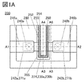
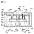
- FIG. 1A is a top view of a semiconductor device which is one embodiment of the present invention.
- 1B to 1D are cross-sectional views of semiconductor devices that are embodiments of the present invention.
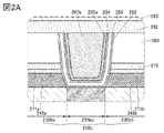
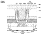
- 2A and 2B are cross-sectional views of a semiconductor device that is one embodiment of the present invention.
- FIG. 3 is a schematic cross-sectional view of a transistor used for calculation.
- 4A and 4B are diagrams showing calculation results.
- FIG. 5A is a diagram showing the calculation model shown in this embodiment.
- FIG. 5B is a diagram showing the calculation results shown in this embodiment.
- 6A and 6B are cross-sectional views of a semiconductor device that is one embodiment of the present invention.
- 7A to 7D are schematic diagrams of aluminum concentration profiles in metal oxides.
- FIG. 8A to 8C are cross-sectional views of semiconductor devices that are one embodiment of the present invention.
- 9A and 9B are diagrams showing band diagrams.
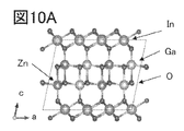
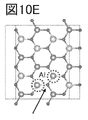
- 10A to 10E are diagrams showing the calculation model shown in this embodiment.
- FIG. 10F is a diagram showing the calculation results shown in this embodiment.
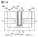
- FIG. 11A is a top view of a semiconductor device which is one embodiment of the present invention.
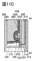
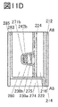
- 11B to 11D are cross-sectional views of semiconductor devices that are one embodiment of the present invention.
- FIG. 12A is a top view of a semiconductor device which is one embodiment of the present invention.
- 12B to 12D are cross-sectional views of semiconductor devices that are one embodiment of the present invention.
- FIG. 13A is a top view of a semiconductor device which is one embodiment of the present invention.
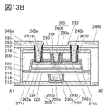
- FIG. 13B to 13D are cross-sectional views of semiconductor devices that are one embodiment of the present invention.
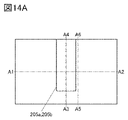
- FIG. 14A is a top view illustrating a method for manufacturing a semiconductor device which is one embodiment of the present invention.
- 14B to 14D are cross-sectional views illustrating a method for manufacturing a semiconductor device which is one embodiment of the present invention.
- FIG. 15A is a top view illustrating a method for manufacturing a semiconductor device which is one embodiment of the present invention.
- 15B to 15D are cross-sectional views illustrating a method for manufacturing a semiconductor device which is one embodiment of the present invention.
- FIG. 16A is a top view illustrating a method for manufacturing a semiconductor device which is one embodiment of the present invention.
- FIG. 16B to 16D are cross-sectional views illustrating a method for manufacturing a semiconductor device which is one embodiment of the present invention.
- FIG. 17A is a top view illustrating a method for manufacturing a semiconductor device which is one embodiment of the present invention.
- 17B to 17D are cross-sectional views illustrating a method for manufacturing a semiconductor device which is one embodiment of the present invention.
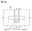
- FIG. 18A is a top view illustrating a method for manufacturing a semiconductor device which is one embodiment of the present invention.
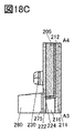
- 18B to 18D are cross-sectional views illustrating a method for manufacturing a semiconductor device which is one embodiment of the present invention.
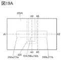
- FIG. 19A is a top view illustrating a method for manufacturing a semiconductor device which is one embodiment of the present invention.
- FIG. 19B to 19D are cross-sectional views illustrating a method for manufacturing a semiconductor device which is one embodiment of the present invention.
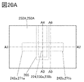
- FIG. 20A is a top view illustrating a method for manufacturing a semiconductor device which is one embodiment of the present invention.
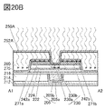
- 20B to 20D are cross-sectional views illustrating a method for manufacturing a semiconductor device which is one embodiment of the present invention.
- FIG. 21A is a top view illustrating a method for manufacturing a semiconductor device which is one embodiment of the present invention.
- 21B to 21D are cross-sectional views illustrating a method for manufacturing a semiconductor device which is one embodiment of the present invention.
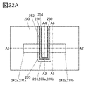
- FIG. 22A is a top view illustrating a method for manufacturing a semiconductor device which is one embodiment of the present invention.
- FIG. 22B to 22D are cross-sectional views illustrating a method for manufacturing a semiconductor device which is one embodiment of the present invention.
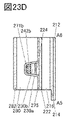
- FIG. 23A is a top view illustrating a method for manufacturing a semiconductor device which is one embodiment of the present invention.
- 23B to 23D are cross-sectional views illustrating a method for manufacturing a semiconductor device which is one embodiment of the present invention.
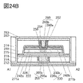
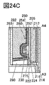
- FIG. 24A is a top view illustrating a method for manufacturing a semiconductor device which is one embodiment of the present invention.
- 24B to 24D are cross-sectional views illustrating a method for manufacturing a semiconductor device which is one embodiment of the present invention.
- FIG. 25A is a top view illustrating a method for manufacturing a semiconductor device which is one embodiment of the present invention.
- FIG. 25B to 25D are cross-sectional views illustrating a method for manufacturing a semiconductor device which is one embodiment of the present invention.
- FIG. 26 is a top view illustrating a microwave processing apparatus according to one embodiment of the present invention.
- FIG. 27 is a cross-sectional view illustrating a microwave processing device according to one aspect of the present invention.
- FIG. 28 is a cross-sectional view illustrating a microwave processing device according to one embodiment of the present invention.
- FIG. 29 is a cross-sectional view illustrating a microwave processing device according to one embodiment of the present invention.
- FIG. 30A is a plan view of a semiconductor device according to one embodiment of the present invention.
- 30B and 30C are cross-sectional views of a semiconductor device that is one embodiment of the present invention.
- FIG. 31 is a diagram showing a circuit diagram of a semiconductor device.
- FIG. 32A is a perspective view of a semiconductor device.
- FIG. 32B is a perspective view explaining the configuration of the semiconductor device.
- FIG. 33 is a cross-sectional view illustrating a structure of a memory device according to one embodiment of the present invention.
- FIG. 34 is a cross-sectional view illustrating a structure of a memory device according to one embodiment of the present invention.
- FIG. 35 is a cross-sectional view of a semiconductor device according to one embodiment of the present invention.
- 36A and 36B are cross-sectional views of semiconductor devices according to one embodiment of the present invention.
- FIG. 37 is a cross-sectional view of a semiconductor device according to one embodiment of the present invention.
- FIG. 38A is a block diagram illustrating a configuration example of a memory device according to one embodiment of the present invention.
- FIG. 38B is a perspective view illustrating a configuration example of a memory device according to one embodiment of the present invention.
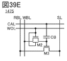
- 39A to 39H are circuit diagrams illustrating configuration examples of memory devices according to one embodiment of the present invention.
- 40A and 40B are schematic diagrams of a semiconductor device according to one embodiment of the present invention.
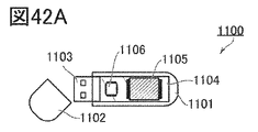
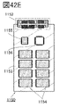
- 41A and 41B are diagrams illustrating an example of an electronic component.
- 42A to 42E are schematic diagrams of a memory device according to one embodiment of the present invention.
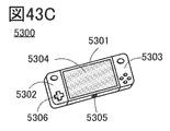
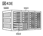
- 43A to 43H are diagrams illustrating electronic devices according to one embodiment of the present invention.
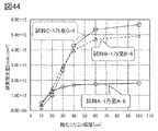
- FIG. 44 is a diagram for explaining the dependence of the oxygen release amount on the thickness of the silicon oxide film.
- FIG. 44 is a diagram for explaining the dependence of the oxygen release amount on the thickness of the silicon oxide film.
- FIG. 45A is a diagram illustrating a cross-sectional STEM image of an aluminum oxide film.
- FIG. 45B is a diagram for explaining the film thickness of the cross section of the aluminum oxide film.
- FIG. 46A is a diagram for explaining the laminated structure of the laminated film.
- FIG. 46B is the SIMS analysis result of the laminated film.
- FIG. 47A is a diagram explaining the structure of an aluminum oxide film.
- FIG. 47B is a diagram for explaining the aluminum oxide film structure dependence of the oxygen release amount.
- FIG. 48A is a cross-sectional STEM image of the sample produced in Example.
- Figures 48B and 48C are the results of EDX analysis of the samples produced in Examples.
- 49A to 49C are the results of SIMS analysis of samples produced in Examples.
- 50 is a diagram showing a top view, a cross-sectional TEM image, and parameters of the TEG produced in Example.
- 51A and 51B show the Id-Vg characteristics of the transistor manufactured in Example.
- 52A and 52B are Vth cumulative probability distributions of the transistors manufactured in Example.
- 53A to 53C show the Id-Vg characteristics of the transistor manufactured in Example.
- 54A to 54C are Vth cumulative probability distributions of the transistors manufactured in Examples.
- 55A to 55C are diagrams showing the relationship between Vth and Id-Vg characteristics of transistors manufactured in Examples.
- FIG. 56A shows the Id-Vg characteristics of the transistor manufactured in Example.
- FIG. 56B is the Vth cumulative probability distribution of the transistor manufactured in Example.
- FIG. 57A shows the Id-Vg characteristics of the transistor manufactured in Example.
- FIG. 57B is the Vth cumulative probability distribution of the transistor manufactured in Example.
- 58A to 58C are diagrams showing the relationship between Vth and Id-Vg characteristics of transistors manufactured in Examples.
- 59A1 to 59C2 are cross-sectional TEM images obtained in Example.
- 60A1 to 60B2 are cross-sectional TEM images obtained in Example.
- FIG. 61 is a diagram for explaining the film thickness of each film before heat treatment and the film thickness of each film after heat treatment.
- FIG. 62A is a diagram explaining the laminated structure of the sample.
- FIG. 62B is a diagram for explaining the sheet resistance of metal oxide.
- FIG. 64A to 63C show the Id-Vg characteristics of the transistors manufactured in Examples.
- 63D to 63F are cross-sectional TEM images of the transistor manufactured in Example.
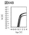
- 64A and 64B are the Id-Vg characteristics of the transistor.
- FIG. 64C is a schematic cross-sectional view of a transistor manufactured in Example.
- FIG. 65 is a diagram for explaining the stress of the conductor formed in the example.
- FIG. 66 is a diagram for explaining the relationship between Ion and stress of a transistor.
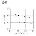
- FIG. 67 is a diagram for explaining the relationship between the ratio of the area of the channel forming region to the area of the source electrode or the drain electrode and the on current.
- FIG. 68A is a diagram explaining the laminated structure of the sample.
- FIG. 68B is a diagram explaining the results of SIMS analysis.
- FIG. 69A is the Id-Vg characteristic of the transistor.
- FIG. 69B is a schematic diagram of oxygen supply to metal oxide.
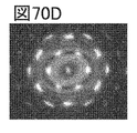
- 70A and 70B are planar TEM images of metal oxides.
- 70C and 70D are FFT images.
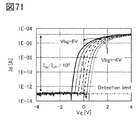
- FIG. 71 shows the Id-Vg characteristics of the transistor manufactured in Example.
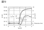
- FIG. 72 shows the Id-Vg characteristics of the transistor manufactured in Example.
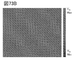
- 73A and 73B are Vth maps of transistors.
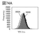
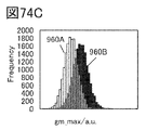
- 74A-74D are histograms of Vth, S value, gm, and Ion of the transistor.
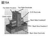
- FIG. 75A is a schematic diagram showing the structure of a prototype transistor.
- FIG. 75A is a schematic diagram showing the structure of a prototype transistor.
- 75B is a cross-sectional view of the prototyped transistor in the channel width direction.
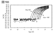
- 76A and 76B are diagrams showing the drain current-top gate voltage characteristics of the prototyped transistor.
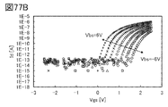
- 77A and 77B are diagrams showing the drain current-top gate voltage characteristics of the prototyped transistor.
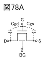
- 78A and 78B are diagrams for explaining capacitance.
- 78C and 78D are diagrams showing the top gate voltage-capacitance characteristics of the prototyped transistor.
- top views also called “plan views”
- perspective views descriptions of some components may be omitted in order to facilitate understanding of the invention. Also, description of some hidden lines may be omitted.
- the ordinal numbers such as first and second are used for convenience and do not indicate the order of steps or the order of stacking. Therefore, for example, “first” can be appropriately replaced with “second” or “third”. Also, the ordinal numbers described in this specification and the like may not match the ordinal numbers used to specify one aspect of the present invention.
- connection relationships other than the connection relationships shown in the drawings or the text are not limited to the predetermined connection relationships, for example, the connection relationships shown in the drawings or the text.
- X and Y are objects (for example, devices, elements, circuits, wiring, electrodes, terminals, conductive films, layers, etc.).
- a transistor is an element having at least three terminals including a gate, a drain, and a source.
- a region in which a channel is formed (hereinafter also referred to as a channel formation region) is provided between the drain (drain terminal, drain region, or drain electrode) and the source (source terminal, source region, or source electrode).
- a current can flow between the source and the drain through the formation region.
- a channel formation region means a region where current mainly flows.
- the function of the source or drain may be switched when using transistors of different polarities or when the direction of current changes in circuit operation. Therefore, in this specification and the like, the terms “source” and “drain” can be used interchangeably in some cases.
- the channel length is, for example, a region in which a semiconductor (or a portion of the semiconductor in which current flows when the transistor is on) overlaps with a gate electrode in a top view of a transistor, or the source length in a channel formation region.
- the channel length does not always have the same value in all regions of one transistor. That is, the channel length of one transistor may not be fixed to one value. Therefore, in this specification, the channel length is any one value, maximum value, minimum value, or average value in the channel forming region.
- the channel width is the region in which the semiconductor (or the portion of the semiconductor where current flows when the transistor is on) and the gate electrode overlap each other, or the channel length direction in the channel formation region.
- a channel width in a region where a channel is actually formed (hereinafter also referred to as an “effective channel width”) and a channel width shown in a top view of a transistor ( hereinafter also referred to as “apparent channel width”) may be different.
- the effective channel width becomes larger than the apparent channel width, and its influence cannot be ignored.
- the proportion of the channel formation region formed on the side surface of the semiconductor may be large. In that case, the effective channel width is larger than the apparent channel width.
- channel width may refer to the apparent channel width.
- channel width may refer to the effective channel width.
- the values of the channel length, channel width, effective channel width, apparent channel width, etc. can be determined by analyzing a cross-sectional TEM image or the like.
- impurities in a semiconductor refer to, for example, substances other than the main components that constitute the semiconductor.
- an element whose concentration is less than 0.1 atomic percent can be said to be an impurity.
- the inclusion of impurities may cause, for example, an increase in the defect level density of the semiconductor, a decrease in crystallinity, and the like.
- impurities that change the characteristics of the semiconductor include, for example, group 1 elements, group 2 elements, group 13 elements, group 14 elements, group 15 elements, and oxide semiconductors.
- transition metals other than the main component such as hydrogen, lithium, sodium, silicon, boron, phosphorus, carbon, and nitrogen.
- water may also function as an impurity.
- oxygen vacancies also referred to as V 2 O 3
- silicon oxynitride contains more oxygen than nitrogen as its composition.
- Silicon nitride oxide contains more nitrogen than oxygen in its composition.
- aluminum oxynitride has a higher content of oxygen than nitrogen as its composition.
- aluminum oxynitride has a composition in which the content of nitrogen is higher than that of oxygen.
- hafnium oxynitride has a higher content of oxygen than nitrogen as its composition.
- hafnium oxynitride has a composition in which the content of nitrogen is higher than that of oxygen.
- insulator can be replaced with an insulating film or an insulating layer.
- conductor can be replaced with a conductive film or a conductive layer.
- semiconductor can be interchanged with a semiconductor film or a semiconductor layer.
- parallel means a state in which two straight lines are arranged at an angle of -10 degrees or more and 10 degrees or less. Therefore, the case of ⁇ 5 degrees or more and 5 degrees or less is also included.
- substantially parallel means a state in which two straight lines are arranged at an angle of -30 degrees or more and 30 degrees or less.
- Perfect means that two straight lines are arranged at an angle of 80 degrees or more and 100 degrees or less. Therefore, the case of 85 degrees or more and 95 degrees or less is also included.
- substantially perpendicular means a state in which two straight lines are arranged at an angle of 60 degrees or more and 120 degrees or less.
- a metal oxide is a metal oxide in a broad sense.
- Metal oxides are classified into oxide insulators, oxide conductors (including transparent oxide conductors), oxide semiconductors (also referred to as oxide semiconductors or simply OSs), and the like.
- oxide semiconductors also referred to as oxide semiconductors or simply OSs
- an OS transistor can be referred to as a transistor including a metal oxide or an oxide semiconductor.
- the term “normally-off” means that the drain current per 1 ⁇ m of the channel width flowing through the transistor when no potential is applied to the gate or when a ground potential is applied to the gate is 1 ⁇ 10 ⁇ 1 at room temperature. 20 A or less, 1 ⁇ 10 ⁇ 18 A or less at 85° C., or 1 ⁇ 10 ⁇ 16 A or less at 125° C.
- Voltage is a potential difference from a reference potential.
- the reference potential is ground potential
- “voltage” can be replaced with “potential”. Note that the ground potential does not necessarily mean 0V.
- the potential is relative, and when the reference potential changes, the potential applied to the wiring, the potential applied to the circuit, etc., and the potential output from the circuit etc. also change.
- substantially the same height indicates a configuration in which the heights from a reference plane (for example, a flat plane such as a substrate surface) are equal in cross-sectional view.
- planarization processing typically CMP (Chemical Mechanical Polishing) processing
- CMP Chemical Mechanical Polishing
- the surfaces to be CMP-processed have the same height from the reference surface.
- approximately matching heights includes cases where the heights match.
- the heights of the layers may differ depending on the processing equipment, processing method, or material of the surface to be processed during the CMP processing.
- this case is also treated as "substantially the same height".
- the height of the top surface of the first layer and the height of the second layer When the difference from the height of the upper surface is 20 nm or less, it is also said that the heights are approximately the same.
- the side surfaces or the edges roughly match means that at least part of the outline overlaps between the upper layer and the lower layer when viewed from the top.
- the upper layer and the lower layer may be processed with the same mask pattern or partially with the same mask pattern.
- flat sides or edges roughly match includes the case where the sides or edges match.
- the contours do not overlap, and the upper contour may be positioned inside the lower contour, or the upper contour may be positioned outside the lower contour. The parts roughly match.”
- FIG. 1A-1D are top and cross-sectional views of a semiconductor device having a transistor 200.
- FIG. 1A is a top view of the semiconductor device.
- 1B to 1D are cross-sectional views of the semiconductor device.
- FIG. 1B is a cross-sectional view of the portion indicated by the dashed-dotted line A1-A2 in FIG. 1A, and is also a cross-sectional view of the transistor 200 in the channel length direction.
- FIG. 1C is a cross-sectional view of the portion indicated by the dashed-dotted line A3-A4 in FIG.
- FIG. 1A is also a cross-sectional view of the transistor 200 in the channel width direction.
- FIG. 1D is sectional drawing of the site
- a semiconductor device of one embodiment of the present invention includes an insulator 212 over a substrate (not shown), an insulator 214 over the insulator 212, a transistor 200 over the insulator 214, and an insulator 280 over the transistor 200. , insulator 282 on insulator 280 , insulator 283 on insulator 282 , insulator 274 on insulator 283 , insulator 285 on insulator 283 and insulator 274 .
- the insulator 212, the insulator 214, the insulator 216, the insulator 280, the insulator 282, the insulator 283, the insulator 285, and the insulator 274 function as interlayer films.
- conductor 240 (a conductor 240a and a conductor 240b) that is electrically connected to the transistor 200 and functions as a plug.
- insulators 241 (insulators 241a and 241b) are provided in contact with side surfaces of conductors 240 functioning as plugs.
- conductors 246 (conductors 246 a and 246 b ) that are electrically connected to the conductor 240 and function as wirings are provided over the insulator 285 and the conductor 240 .
- the insulator 283 is in contact with part of the top surface of the insulator 214, the side surface of the insulator 216, the side surface of the insulator 222, the side surface of the insulator 275, the side surface of the insulator 280, and the side surface and top surface of the insulator 282. .
- An insulator 241a is provided in contact with the inner wall of the opening of the insulator 280, the insulator 282, the insulator 283, and the insulator 285, and the conductor 240a is provided in contact with the side surface of the insulator 241a.
- An insulator 241b is provided in contact with the inner wall of the opening of the insulator 280, the insulator 282, the insulator 283, and the insulator 285, and the conductor 240b is provided in contact with the side surface of the insulator 241b.
- the insulator 241 has a structure in which a first insulator is provided in contact with the inner wall of the opening, and a second insulator is provided inside.
- the conductor 240 has a structure in which a first conductor is provided in contact with the side surface of the insulator 241 and a second conductor is provided inside.
- the height of the top surface of the conductor 240 and the height of the top surface of the insulator 285 in the region overlapping with the conductor 246 are approximately the same.
- the transistor 200 shows a structure in which the first insulator of the insulator 241 and the second insulator of the insulator 241 are stacked, the present invention is not limited to this.
- the insulator 241 may be provided as a single layer or a stacked structure of three or more layers.
- the transistor 200 shows the structure in which the first conductor of the conductor 240 and the second conductor of the conductor 240 are stacked, the present invention is not limited to this.
- the conductor 240 may be provided as a single layer or a laminated structure of three or more layers. When the structure has a laminated structure, an ordinal number may be assigned in order of formation for distinction.
- the transistor 200 includes an insulator 216 over the insulator 214, conductors 205 (a conductor 205a and a conductor 205b) embedded in the insulator 216, and an insulating material.
- the insulator 252 includes the top surface of the insulator 222, the sides of the insulator 224, the sides of the oxide 230a, the sides and top of the oxide 230b, the sides of the conductor 242, It contacts the side surface of the insulator 271 , the side surface of the insulator 275 , the side surface of the insulator 280 , and the bottom surface of the insulator 250 .
- the top surface of the conductor 260 is arranged so that the top surface of the insulator 254 , the top surface of the insulator 250 , the top surface of the insulator 252 , and the top surface of the insulator 280 are substantially flush with each other.
- the insulator 282 is in contact with at least part of the upper surface of each of the conductor 260 , the insulator 252 , the insulator 250 , the insulator 254 , and the insulator 280 .
- oxide 230a and the oxide 230b may be collectively referred to as the oxide 230 below.
- the conductor 242a and the conductor 242b are collectively referred to as the conductor 242 in some cases.
- the insulator 271a and the insulator 271b are collectively referred to as the insulator 271 .
- the insulator 280 and the insulator 275 are provided with openings reaching the oxide 230b.
- An insulator 252, an insulator 250, an insulator 254, and a conductor 260 are positioned within the opening.
- a conductor 260, an insulator 252, an insulator 250, and an insulator 254 are provided between the insulator 271a and the conductor 242a and the insulator 271b and the conductor 242b.
- the insulator 254 has a region in contact with the side surface of the conductor 260 and a region in contact with the bottom surface of the conductor 260 .
- the oxide 230 preferably has an oxide 230a overlying the insulator 224 and an oxide 230b overlying the oxide 230a.
- the transistor 200 has a structure in which the oxide 230 has two layers of the oxide 230a and the oxide 230b stacked, the present invention is not limited to this.
- a single layer of the oxide 230b or a layered structure of three or more layers may be provided, or each of the oxides 230a and 230b may have a layered structure.
- the conductor 260 functions as a first gate (also called top gate) electrode, and the conductor 205 functions as a second gate (also called back gate) electrode.
- insulators 252, 250, and 254 function as a first gate insulator
- insulators 222 and 224 function as a second gate insulator.
- the gate insulator is sometimes called a gate insulating layer or a gate insulating film.
- the conductor 242a functions as one of the source electrode and the drain electrode
- the conductor 242b functions as the other of the source electrode and the drain electrode. At least part of the region of the oxide 230 overlapping with the conductor 260 functions as a channel formation region.
- FIG. 2A shows an enlarged view of the vicinity of the channel forming region in FIG. 1B.
- the oxide 230b includes a region 230bc functioning as a channel formation region of the transistor 200, and regions 230ba and 230bb functioning as a source region or a drain region and provided to sandwich the region 230bc.
- the region 230bc overlaps the conductor 260 .
- the region 230bc is provided in a region between the conductors 242a and 242b.
- the region 230ba is provided so as to overlap with the conductor 242a
- the region 230bb is provided so as to overlap with the conductor 242b.
- region 230bc functioning as a channel forming region is a high-resistance region with a lower carrier concentration because it has less oxygen vacancies or a lower impurity concentration than the regions 230ba and 230bb.
- region 230bc can be said to be i-type (intrinsic) or substantially i-type.
- the region 230ba and the region 230bb functioning as a source region or a drain region have many oxygen vacancies or have a high impurity concentration such as hydrogen, nitrogen, or a metal element, so that the carrier concentration is increased and the resistance is lowered.
- the regions 230ba and 230bb are n-type regions having a higher carrier concentration and a lower resistance than the region 230bc.
- the carrier concentration of the region 230bc functioning as a channel formation region is preferably 1 ⁇ 10 18 cm ⁇ 3 or less, more preferably less than 1 ⁇ 10 17 cm ⁇ 3 , and 1 ⁇ 10 16 cm It is more preferably less than ⁇ 3 , more preferably less than 1 ⁇ 10 13 cm ⁇ 3 , even more preferably less than 1 ⁇ 10 12 cm ⁇ 3 .
- the lower limit of the carrier concentration of the region 230bc functioning as a channel forming region is not particularly limited, but can be, for example, 1 ⁇ 10 ⁇ 9 cm ⁇ 3 .
- the carrier concentration is equal to or lower than the carrier concentration of the region 230ba and the region 230bb, and equal to or higher than the carrier concentration of the region 230bc.
- a region may be formed. That is, the region functions as a junction region between the region 230bc and the region 230ba or the region 230bb.
- the bonding region may have a hydrogen concentration equal to or lower than that of the regions 230ba and 230bb and equal to or higher than that of the region 230bc.
- the bonding region may have oxygen vacancies equal to or less than those of the regions 230ba and 230bb and equal to or greater than those of the region 230bc.
- FIG. 2A shows an example in which the regions 230ba, 230bb, and 230bc are formed in the oxide 230b
- the present invention is not limited to this.
- each of the above regions may be formed up to oxide 230a as well as oxide 230b.
- the concentrations of metal elements and impurity elements such as hydrogen and nitrogen detected in each region are not limited to stepwise changes for each region, and may change continuously within each region. In other words, the closer the region is to the channel formation region, the lower the concentrations of the metal elements and the impurity elements such as hydrogen and nitrogen.
- a metal oxide functioning as a semiconductor (hereinafter also referred to as an oxide semiconductor) is preferably used for the oxide 230 (the oxide 230a and the oxide 230b) including a channel formation region.
- the bandgap of the metal oxide that functions as a semiconductor is preferably 2 eV or more, more preferably 2.5 eV or more.
- the off-state current of the transistor can be reduced by using a metal oxide with a large bandgap.
- an In-M-Zn oxide containing indium, element M and zinc (element M is aluminum, gallium, yttrium, tin, copper, vanadium, beryllium, boron, titanium, iron, nickel, germanium , zirconium, molybdenum, lanthanum, cerium, neodymium, hafnium, tantalum, tungsten, or magnesium).
- element M is aluminum, gallium, yttrium, tin, copper, vanadium, beryllium, boron, titanium, iron, nickel, germanium , zirconium, molybdenum, lanthanum, cerium, neodymium, hafnium, tantalum, tungsten, or magnesium.
- an In--Ga oxide, an In--Zn oxide, or an indium oxide may be used.
- the oxide 230 preferably has a laminated structure of multiple oxide layers with different chemical compositions.
- the atomic ratio of the element M to the main component metal element is the same as the atomic ratio of the element M to the main component metal element in the metal oxide used for the oxide 230b. Larger is preferable.
- the atomic ratio of the element M to In is preferably higher than the atomic ratio of the element M to In in the metal oxide used for the oxide 230b. With this structure, diffusion of impurities and oxygen from structures formed below the oxide 230a to the oxide 230b can be suppressed.
- the atomic ratio of In to the element M is preferably higher than the atomic ratio of In to the element M in the metal oxide used for the oxide 230a.
- the transistor 200 can have high on-state current and high frequency characteristics.
- the oxides 230a and 230b have a common element other than oxygen as a main component, the defect level density at the interface between the oxides 230a and 230b can be reduced. Since the defect level density at the interface between the oxides 230a and 230b can be reduced, the effect of interface scattering on carrier conduction is small, and a high on-current can be obtained.
- the neighboring composition includes a range of ⁇ 30% of the desired atomic number ratio.
- the element M it is preferable to use gallium.
- a metal oxide that can be used for the oxide 230a may be used as the oxide 230b.
- the above atomic ratio is not limited to the atomic ratio of the deposited metal oxide, and the atomic ratio of the sputtering target used for the deposition of the metal oxide. may be
- the oxide 230b preferably has crystallinity.
- CAAC-OS c-axis aligned crystal oxide semiconductor
- CAAC-OS is a metal oxide that has a dense structure with high crystallinity and few impurities and defects (eg, oxygen vacancies (V 2 O 3 ) and the like).
- heat treatment is performed at a temperature at which the metal oxide does not become polycrystalline (for example, 400° C. or higher and 600° C. or lower), so that the CAAC-OS has a dense structure with higher crystallinity.
- a temperature at which the metal oxide does not become polycrystalline for example, 400° C. or higher and 600° C. or lower
- the oxide 230b by using a crystalline oxide such as CAAC-OS as the oxide 230b, extraction of oxygen from the oxide 230b by the source electrode or the drain electrode can be suppressed. Accordingly, extraction of oxygen from the oxide 230b can be reduced even if heat treatment is performed, so that the transistor 200 is stable against high temperatures (so-called thermal budget) in the manufacturing process.
- a crystalline oxide such as CAAC-OS
- a transistor including an oxide semiconductor if impurities and oxygen vacancies are present in a region where a channel is formed in the oxide semiconductor, electrical characteristics are likely to vary, and reliability may be degraded.
- hydrogen in the vicinity of oxygen vacancies may form defects in which hydrogen enters oxygen vacancies (hereinafter sometimes referred to as V OH ) to generate electrons serving as carriers. Therefore, if oxygen vacancies are included in the region where the channel is formed in the oxide semiconductor, the transistor has normally-on characteristics (the channel exists even if no voltage is applied to the gate electrode, and current flows through the transistor). flow characteristics). Therefore, impurities, oxygen vacancies, and VOH are preferably reduced as much as possible in a region where a channel is formed in the oxide semiconductor. In other words, the region in which the channel is formed in the oxide semiconductor preferably has a reduced carrier concentration and is i-type (intrinsic) or substantially i-type.
- an insulator containing oxygen that is released by heating (hereinafter sometimes referred to as excess oxygen) is provided in the vicinity of the oxide semiconductor, and heat treatment is performed so that the oxide semiconductor is converted from the insulator.
- Oxygen can be supplied and oxygen vacancies and VOH can be reduced.
- the on-state current or the field-effect mobility of the transistor 200 might decrease.
- variations in the amount of oxygen supplied to the source region or the drain region within the substrate surface cause variations in the characteristics of the semiconductor device having transistors.
- the region 230bc functioning as a channel formation region preferably has a reduced carrier concentration and is i-type or substantially i-type.
- Region 230bb has a high carrier concentration and is preferably n-type. In other words, it is preferable to reduce oxygen vacancies and VOH in the region 230bc of the oxide semiconductor and prevent an excessive amount of oxygen from being supplied to the regions 230ba and 230bb .
- the region 230ba and the region 230bb functioning as a source region or a drain region preferably have a high carrier concentration and are n-type.
- the concentration is reduced and is i-type or substantially i-type.
- the n-type region preferably does not extend into the channel forming region.
- the device simulation was performed using Synopsys TCAD Sentaurus.
- a schematic cross-sectional view of a transistor used for the device simulation is shown in FIG.
- the transistor includes an oxide semiconductor (OS), a source electrode (Source) and a drain electrode (Drain) over the oxide semiconductor, and a gate electrode (Gate) overlapping with the oxide semiconductor.
- OS oxide semiconductor
- Source source electrode
- Drain drain electrode
- Gate gate electrode
- LSD shown in FIG. 3 is the distance between the source and drain electrodes.
- ⁇ L shown in FIG. 3 is the length of the n-type region extending from the end of the source or drain electrode to the channel formation region.
- LSD was set to 60 nm, 120 nm, or 240 nm.
- ⁇ L was set to 0 nm, 5 nm, 10 nm, 20 nm, or 30 nm.
- the donor concentration Nd of the source region, the drain region, and the n -type region was set to 1 ⁇ 10 19 cm ⁇ 3 or 5 ⁇ 10 19 cm ⁇ 3 .
- the channel width was set to 60 nm.
- FIGS. 4A and 4B The device simulation results are shown in FIGS. 4A and 4B.
- FIG. 4A shows the results when the donor concentration Nd of the source region, the drain region, and the n -type region is 1 ⁇ 10 19 cm ⁇ 3
- FIG. This is the result when the donor concentration Nd of the region is 5 ⁇ 10 19 cm ⁇ 3 .
- the vertical axis indicates the amount of change in threshold voltage ( ⁇ Vth) [V], and the horizontal axis indicates ⁇ L [nm].
- the threshold voltage (Vth) is defined as the gate voltage Vg when the drain current becomes 1 pA.
- the plots indicated by circles are the results when the LSD is 240 nm
- the plots indicated by squares are the results when the LSD is 120 nm
- the plots indicated by diamonds are the LSD . These are the results when the thickness is set to 60 nm.
- the n-type region preferably does not extend into the channel forming region.
- microwave treatment is performed in an atmosphere containing oxygen with the conductors 242a and 242b provided over the oxide 230b, so that oxygen vacancies in the region 230bc and VOH are reduced.
- the microwave treatment refers to treatment using an apparatus having a power supply for generating high-density plasma using microwaves, for example.
- oxygen gas By performing microwave treatment in an atmosphere containing oxygen, oxygen gas can be converted into plasma using microwaves or high frequencies such as RF, and the oxygen plasma can act. At this time, the region 230bc can also be irradiated with microwaves or high frequencies such as RF.
- V OH in the region 230bc is divided into oxygen vacancies (V 0 ) and hydrogen ( H ), the hydrogen is removed from the region 230bc, and the oxygen vacancies are compensated with oxygen. can be done. Therefore, the hydrogen concentration, oxygen vacancies, and VOH in the region 230bc can be reduced, and the carrier concentration can be lowered.
- the effects of microwaves, high frequencies such as RF, oxygen plasma, etc. are shielded by the conductors 242a and 242b and do not reach the regions 230ba and 230bb.
- the effect of oxygen plasma can be reduced by insulators 271 and 280 provided over oxide 230b and conductor 242.
- FIG. 1 V OH is reduced and an excessive amount of oxygen is not supplied in the regions 230ba and 230bb during the microwave treatment, so that a decrease in carrier concentration can be prevented.
- microwave treatment is preferably performed in an oxygen-containing atmosphere.
- an atmosphere containing oxygen By performing microwave treatment in an atmosphere containing oxygen through the insulator 252 or the insulator 250 in this manner, oxygen can be efficiently injected into the region 230bc.
- the insulator 252 so as to be in contact with the side surface of the conductor 242 and the surface of the region 230bc, it is possible to suppress the injection of more than a necessary amount of oxygen into the region 230bc and suppress the oxidation of the side surface of the conductor 242. .
- oxidation of the side surface of the conductor 242 can be suppressed when the insulating film to be the insulator 250 is formed.
- the oxygen injected into the region 230bc has various forms such as oxygen atoms, oxygen molecules, and oxygen radicals (also called O radicals, atoms, molecules, or ions having unpaired electrons).
- the oxygen injected into the region 230bc may be one or more of the above forms, and oxygen radicals are particularly preferable.
- the film quality of the insulator 252 and the insulator 250 can be improved, the reliability of the transistor 200 is improved.
- oxygen vacancies and V OH can be selectively removed from the oxide semiconductor region 230bc to make the region 230bc i-type or substantially i-type. Furthermore, excessive supply of oxygen to the regions 230ba and 230bb functioning as the source region or the drain region can be suppressed, and the state of the n-type region before the microwave treatment can be maintained. As a result, variations in the electrical characteristics of the transistor 200 can be suppressed, and variation in the electrical characteristics of the transistor 200 within the substrate surface can be suppressed.
- a semiconductor device with little variation in transistor characteristics can be provided by adopting the configuration described above. Moreover, a highly reliable semiconductor device can be provided. Moreover, a semiconductor device having favorable electrical characteristics can be provided.
- a curved surface may be provided between the side surface of the oxide 230b and the top surface of the oxide 230b in a cross-sectional view of the transistor 200 in the channel width direction. That is, the end of the side surface and the end of the upper surface may be curved (hereinafter also referred to as round shape).
- the radius of curvature of the curved surface is preferably larger than 0 nm and smaller than the film thickness of the oxide 230b in the region overlapping with the conductor 242, or smaller than half the length of the region without the curved surface.
- the radius of curvature of the curved surface is greater than 0 nm and less than or equal to 20 nm, preferably greater than or equal to 1 nm and less than or equal to 15 nm, and more preferably greater than or equal to 2 nm and less than or equal to 10 nm.
- the interface between the oxide 230 and the insulator 252 and its vicinity can be Indium contained in the oxide 230 may be unevenly distributed.
- the vicinity of the surface of the oxide 230 has an atomic ratio close to that of indium oxide or an atomic ratio close to that of In—Zn oxide.
- the defect level density at the interface between the oxide 230a and the oxide 230b can be reduced. Therefore, the influence of interface scattering on carrier conduction is reduced, and the transistor 200 can obtain a large on-current and high frequency characteristics.
- At least one of the insulator 212 , the insulator 214 , the insulator 271 , the insulator 275 , the insulator 282 , the insulator 283 , and the insulator 285 is exposed to impurities such as water and hydrogen from the substrate side or the transistor 200 . It preferably functions as a barrier insulating film that suppresses diffusion from above into the transistor 200 .
- At least one of the insulators 212, 214, 271, 275, 282, 283, and 285 is a hydrogen atom, a hydrogen molecule, a water molecule, a nitrogen atom, a nitrogen molecule, It is preferable to use an insulating material that has a function of suppressing the diffusion of impurities such as nitrogen oxide molecules (N 2 O, NO, NO 2 , etc.) and copper atoms (thus, the above impurities hardly permeate). Alternatively, it is preferable to use an insulating material that has a function of suppressing the diffusion of oxygen (eg, at least one of oxygen atoms, oxygen molecules, and the like) (the oxygen hardly permeates).
- an insulating material that has a function of suppressing the diffusion of oxygen eg, at least one of oxygen atoms, oxygen molecules, and the like
- a barrier insulating film refers to an insulating film having barrier properties.
- barrier property refers to the function of suppressing the diffusion of the corresponding substance (also referred to as “low permeability”).
- the corresponding substance has the function of capturing and fixing (also called gettering).
- the insulators 212, 214, 271, 275, 282, 283, and 285 are insulators having a function of suppressing diffusion of water, impurities such as hydrogen, and oxygen. is preferably used, and for example, aluminum oxide, magnesium oxide, hafnium oxide, gallium oxide, indium gallium zinc oxide, silicon nitride, or silicon nitride oxide can be used.
- the insulator 212, the insulator 275, and the insulator 283 are preferably made of silicon nitride or the like, which has a higher hydrogen barrier property.
- the insulator 214, the insulator 271, the insulator 282, and the insulator 285 are preferably made of aluminum oxide, magnesium oxide, or the like, which has high functions of capturing and fixing hydrogen.
- impurities such as water and hydrogen can be prevented from diffusing from the substrate side to the transistor 200 side through the insulators 212 and 214 .
- impurities such as water and hydrogen can be prevented from diffusing toward the transistor 200 from an interlayer insulating film or the like arranged outside the insulator 285 .
- diffusion of oxygen contained in the insulator 224 or the like to the substrate side through the insulators 212 and 214 can be suppressed.
- oxygen contained in the insulator 280 or the like can be prevented from diffusing above the transistor 200 through the insulator 282 or the like.
- the transistor 200 is formed of the insulators 212, 214, 271, 275, 282, 283, and 283, which have a function of suppressing diffusion of water, impurities such as hydrogen, and oxygen.
- a structure surrounded by an insulator 285 is preferable.
- the insulators 212, 214, 271, 275, 282, 283, and 285 are preferably oxides having an amorphous structure.
- metal oxides such as AlO x (x is any number greater than 0) or MgO y (y is any number greater than 0).
- Oxygen atoms in metal oxides having such an amorphous structure have dangling bonds, and the dangling bonds sometimes have the property of capturing or fixing hydrogen.
- hydrogen contained in the transistor 200 or hydrogen existing around the transistor 200 is captured or fixed. be able to.
- the transistor 200 and the semiconductor device with favorable characteristics and high reliability can be manufactured.
- the insulators 212, 214, 271, 275, 282, 283, and 285 preferably have an amorphous structure, but part of the insulator 212, the insulator 214, the insulator 271, the insulator 275, the insulator 282, the insulator 283, and the insulator 285 has a polycrystalline structure. may be formed.
- the insulator 212, the insulator 214, the insulator 271, the insulator 275, the insulator 282, the insulator 283, and the insulator 285 are multilayers in which a layer having an amorphous structure and a layer having a polycrystalline structure are stacked. It may be a structure. For example, a laminated structure in which a layer of polycrystalline structure is formed on a layer of amorphous structure may be used.
- the insulators 212, 214, 271, 275, 282, 283, and 285 may be deposited by sputtering, for example. Since the sputtering method does not require the use of molecules containing hydrogen in the deposition gas, the hydrogen concentrations of the insulators 212, 214, 271, 275, 282, 283, and 285 are can be reduced.
- the film formation method is not limited to the sputtering method, chemical vapor deposition (CVD) method, molecular beam epitaxy (MBE) method, pulsed laser deposition (PLD) method. ) method, Atomic Layer Deposition (ALD) method, or the like may be used as appropriate.
- insulators 212, 275, and 283 It may also be desirable to reduce the resistivity of insulators 212, 275, and 283.
- the resistivity of the insulator 212, the insulator 275, and the insulator 283 can be approximately 1 ⁇ 10 13 ⁇ cm, the insulator 212, the insulator 275, and the insulator 283 can be processed using plasma or the like in a manufacturing process of a semiconductor device. Insulator 283 can mitigate charge-up in conductor 205, conductor 242, conductor 260, or conductor 246 in some cases.
- Each of the insulator 212, the insulator 275, and the insulator 283 preferably has a resistivity of 1 ⁇ 10 10 ⁇ cm or more and 1 ⁇ 10 15 ⁇ cm or less.
- the insulator 216, the insulator 274, the insulator 280, and the insulator 285 preferably have a lower dielectric constant than the insulator 214.
- the parasitic capacitance generated between wirings can be reduced.
- the insulator 216, the insulator 274, the insulator 280, and the insulator 285 include silicon oxide, silicon oxynitride, silicon oxide to which fluorine is added, silicon oxide to which carbon is added, silicon oxide to which carbon and nitrogen are added, Silicon oxide having vacancies or the like may be used as appropriate.
- the conductor 205 is arranged so as to overlap with the oxide 230 and the conductor 260 .
- the conductor 205 is preferably embedded in an opening formed in the insulator 216 . Also, part of the conductor 205 is embedded in the insulator 214 in some cases.
- the conductor 205 has a conductor 205a and a conductor 205b.
- Conductor 205 a is provided in contact with the bottom and side walls of the opening formed in insulator 216 .
- the conductor 205b is provided so as to be embedded in a recess formed in the conductor 205a.
- the height of the top surface of the conductor 205b approximately matches the height of the top surface of the conductor 205a and the height of the top surface of the insulator 216 .
- the conductor 205a has a function of suppressing diffusion of impurities such as hydrogen atoms, hydrogen molecules, water molecules, nitrogen atoms, nitrogen molecules, nitrogen oxide molecules (such as N 2 O, NO, NO 2 ), and copper atoms. It is preferable to use a conductive material having a Alternatively, a conductive material having a function of suppressing diffusion of oxygen (eg, at least one of oxygen atoms and oxygen molecules) is preferably used.
- the conductor 205a By using a conductive material having a function of reducing diffusion of hydrogen for the conductor 205a, impurities such as hydrogen contained in the conductor 205b are prevented from diffusing into the oxide 230 through the insulator 224 or the like. can be prevented. In addition, by using a conductive material having a function of suppressing diffusion of oxygen for the conductor 205a, it is possible to suppress a decrease in conductivity due to oxidation of the conductor 205b. As the conductive material having a function of suppressing diffusion of oxygen, titanium, titanium nitride, tantalum, tantalum nitride, ruthenium, ruthenium oxide, or the like is preferably used, for example. Therefore, the conductor 205a may be a single layer or a laminate of the above conductive materials. For example, the conductor 205a may be titanium nitride.
- a conductive material containing tungsten, copper, or aluminum as its main component is preferably used for the conductor 205b.
- tungsten may be used for the conductor 205b.
- the conductor 205 may function as a second gate electrode.
- the threshold voltage (Vth) of the transistor 200 can be controlled by changing the potential applied to the conductor 205 independently of the potential applied to the conductor 260 .
- Vth of the transistor 200 can be increased and off-state current can be reduced. Therefore, applying a negative potential to the conductor 205 can make the drain current smaller when the potential applied to the conductor 260 is 0 V than when no potential is applied.
- the electric resistivity of the conductor 205 is designed in consideration of the potential applied to the conductor 205, and the film thickness of the conductor 205 is set according to the electric resistivity. Also, the thickness of the insulator 216 is almost the same as that of the conductor 205 . Here, it is preferable to reduce the film thickness of the conductor 205 and the insulator 216 within the range allowed by the design of the conductor 205 . By reducing the thickness of the insulator 216, the absolute amount of impurities such as hydrogen contained in the insulator 216 can be reduced;
- the conductor 205 is preferably provided larger than a region of the oxide 230 that does not overlap with the conductors 242a and 242b, as shown in FIG. 1A.
- the conductor 205 preferably extends also in regions outside the ends of the oxides 230a and 230b in the channel width direction.
- the conductor 205 and the conductor 260 preferably overlap with each other with an insulator interposed therebetween on the outside of the side surface of the oxide 230 in the channel width direction.
- the electric field of the conductor 260 functioning as the first gate electrode and the electric field of the conductor 205 functioning as the second gate electrode electrically surround the channel formation region of the oxide 230 .
- a transistor structure in which a channel formation region is electrically surrounded by electric fields of a first gate and a second gate is referred to as a surrounded channel (S-channel) structure.
- a transistor with an S-channel structure represents a transistor structure in which a channel formation region is electrically surrounded by electric fields of one and the other of a pair of gate electrodes.
- the S-channel structure disclosed in this specification and the like is different from the Fin type structure and the planar type structure.
- the transistor can have increased resistance to the short channel effect, in other words, a transistor in which the short channel effect is less likely to occur.
- the transistor 200 By setting the transistor 200 to be normally off and having the above S-channel structure, the channel formation region can be electrically surrounded. Therefore, the transistor 200 can also be regarded as having a GAA (Gate All Around) structure or an LGAA (Lateral Gate All Around) structure.
- GAA Gate All Around
- LGAA Layer Advanced Gate All Around
- a channel formation region formed at or near the interface between the oxide 230 and the gate insulator is the entire bulk of the oxide 230. can be done. Therefore, since the density of the current flowing through the transistor can be increased, it can be expected that the on-state current of the transistor or the field-effect mobility of the transistor can be increased.
- the conductor 205 is extended to function as wiring.
- a structure in which a conductor functioning as a wiring is provided under the conductor 205 may be employed.
- one conductor 205 does not necessarily have to be provided for each transistor.
- the conductor 205 may be shared by a plurality of transistors.
- the conductor 205 has a structure in which the conductor 205a and the conductor 205b are stacked; however, the present invention is not limited to this.
- the conductor 205 may be provided as a single layer or a laminated structure of three or more layers.
- the insulator 222 and the insulator 224 function as gate insulators.
- the insulator 222 preferably has a function of suppressing diffusion of hydrogen (for example, at least one of hydrogen atoms and hydrogen molecules). Further, the insulator 222 preferably has a function of suppressing diffusion of oxygen (eg, at least one of oxygen atoms, oxygen molecules, and the like). For example, the insulator 222 preferably has a function of suppressing diffusion of one or both of hydrogen and oxygen more than the insulator 224 does.
- hydrogen for example, at least one of hydrogen atoms and hydrogen molecules
- oxygen eg, at least one of oxygen atoms, oxygen molecules, and the like.
- the insulator 222 preferably has a function of suppressing diffusion of one or both of hydrogen and oxygen more than the insulator 224 does.
- the insulator 222 it is preferable to use an insulator containing oxides of one or both of aluminum and hafnium, which are insulating materials.
- the insulator aluminum oxide, hafnium oxide, an oxide containing aluminum and hafnium (hafnium aluminate), or the like is preferably used.
- the conductor 205 can be prevented from reacting with oxygen contained in the insulator 224 and the oxide 230 .
- aluminum oxide, bismuth oxide, germanium oxide, niobium oxide, silicon oxide, titanium oxide, tungsten oxide, yttrium oxide, or zirconium oxide may be added to the insulator.
- these insulators may be nitrided.
- these insulators may be stacked with silicon oxide, silicon oxynitride, or silicon nitride.
- the insulator 222 may be a single layer or a stack of insulators containing so-called high-k materials such as aluminum oxide, hafnium oxide, tantalum oxide, zirconium oxide, and hafnium zirconium oxide.
- high-k materials such as aluminum oxide, hafnium oxide, tantalum oxide, zirconium oxide, and hafnium zirconium oxide.
- thinning of gate insulators may cause problems such as leakage current.
- the gate potential during transistor operation can be reduced while maintaining the physical film thickness.
- a substance with a high dielectric constant such as lead zirconate titanate (PZT), strontium titanate (SrTiO 3 ), (Ba, Sr)TiO 3 (BST) may be used in some cases.
- silicon oxide, silicon oxynitride, or the like may be used as appropriate.
- the heat treatment may be performed at, for example, 100° C. to 600° C., more preferably 350° C. to 550° C.
- the heat treatment is performed in a nitrogen gas atmosphere, an inert gas atmosphere, or an atmosphere containing 10 ppm or more, 1% or more, or 10% or more of an oxidizing gas.
- heat treatment is preferably performed in an oxygen atmosphere. Accordingly, oxygen can be supplied to the oxide 230 to reduce oxygen vacancies.
- the heat treatment may be performed in an atmosphere containing 10 ppm or more, 1% or more, or 10% or more of an oxidizing gas in order to compensate for desorbed oxygen after the heat treatment is performed in a nitrogen gas or inert gas atmosphere. good.
- heat treatment may be continuously performed in a nitrogen gas or inert gas atmosphere.
- oxygen vacancies in the oxide 230 can be repaired with supplied oxygen. Furthermore, the supplied oxygen reacts with the hydrogen remaining in the oxide 230, so that the hydrogen can be removed as H 2 O (dehydrated). This can suppress recombination of hydrogen remaining in the oxide 230 with oxygen vacancies to form VOH.
- the insulator 222 and the insulator 224 may have a laminated structure of two or more layers. In that case, it is not limited to a laminated structure made of the same material, and a laminated structure made of different materials may be used.
- the insulator 224 may be formed in an island shape so as to overlap with the oxide 230a. In this case, the insulator 275 is in contact with the side surface of the insulator 224 and the top surface of the insulator 222 .
- an island shape means a state in which two or more layers formed in the same process and using the same material are physically separated.
- a conductor 242a and a conductor 242b are provided in contact with the top surface of the oxide 230b.
- the conductors 242a and 242b function as the source and drain electrodes of the transistor 200, respectively.
- Examples of the conductor 242 include nitride containing tantalum, nitride containing titanium, nitride containing molybdenum, nitride containing tungsten, nitride containing tantalum and aluminum, and titanium. and a nitride containing aluminum is preferably used.
- nitrides containing tantalum are particularly preferred.
- ruthenium oxide, ruthenium nitride, an oxide containing strontium and ruthenium, an oxide containing lanthanum and nickel, or the like may be used. These materials are preferable because they are conductive materials that are difficult to oxidize or materials that maintain conductivity even after absorbing oxygen.
- hydrogen contained in the oxide 230b and the like might diffuse into the conductor 242a or the conductor 242b.
- hydrogen contained in the oxide 230b or the like easily diffuses into the conductor 242a or the conductor 242b, and the diffused hydrogen 242a or the conductor 242b. That is, hydrogen contained in the oxide 230b or the like might be absorbed by the conductor 242a or the conductor 242b.
- the conductor 242 without the curved surface, the cross-sectional area of the conductor 242 in the cross section in the channel width direction as shown in FIG. 1D can be increased. Accordingly, the conductivity of the conductor 242 can be increased, and the on current of the transistor 200 can be increased.
- the sheet resistance of the oxide 230b in a region overlapping with the conductor 242a (the conductor 242b) is reduced.
- the carrier concentration may increase. Therefore, the resistance of the oxide 230b in the region overlapping with the conductor 242a (the conductor 242b) can be reduced in a self-aligning manner.
- the conductor 242 is preferably formed using a conductive film having compressive stress.
- a strain expanding in the direction of tension (hereinafter sometimes referred to as tensile strain) can be formed in the regions 230ba and 230bb.
- tensile strain a strain expanding in the direction of tension
- the regions 230ba and 230bb can be made into stable n-type regions.
- the compressive stress of the conductor 242 is a stress that tends to relax the compressed shape of the conductor 242, and is a stress that has a vector in the direction from the center to the end of the conductor 242.
- the magnitude of the compressive stress of the conductor 242 is, for example, 500 MPa or more, preferably 1000 MPa or more, more preferably 1500 MPa or more, and even more preferably 2000 MPa or more. Note that the magnitude of the stress of the conductor 242 may be determined by measuring the stress of a sample obtained by forming a conductive film used for the conductor 242 over a substrate.
- a strain is formed in each of the regions 230ba and 230bb by the action of the compressive stress that the conductor 242 has.
- the strain is a strain (tensile strain) expanded in the pulling direction by the action of the compressive stress of the conductor 242 .
- the strain corresponds to stretching of the CAAC structure in a direction perpendicular to the c-axis.
- the strain facilitates the formation of oxygen vacancies and VOH, which easily assume a stable structure.
- the regions 230ba and 230bb become stable n-type regions with high carrier concentrations.
- the present invention is not limited to this.
- a similar strain may form in oxide 230a.
- a model of In-Ga-Zn oxide with a single crystal structure is prepared as a calculation model of strain in metal oxides.
- a model of an In--Ga--Zn oxide with a single crystal structure is referred to as an sc-IGZO model.
- the sc-IGZO model is shown in FIG. 5A.
- the sc-IGZO model consists of 112 atoms.
- three types of models with different lattice constants in the direction perpendicular to the c-axis are prepared. In other words, for the sc-IGZO model, three types of models with different lattice constants in the a-axis direction and the b-axis direction are prepared.
- the rate of change of the lattice constant in the direction perpendicular to the c-axis of each sc-IGZO model is set to 0%, 1%, and 2%.
- the lattice constant in the c-axis direction is fixed.
- the sc-IGZO model with a lattice constant change rate of 1% or 2% in the direction perpendicular to the c-axis is a model in which tensile strain is formed in the metal oxide. Also, by changing the lattice constant in the direction perpendicular to the c-axis by 1%, a stress of about 3.3 GPa is generated in the direction perpendicular to the c-axis and about 2.3 GPa in the c-axis direction.
- each of the sc-IGZO models has oxygen vacancies.
- this model may be referred to as an sc-IGZO model including oxygen deficiency.
- an oxygen vacancy formed by removing an oxygen atom bonded to indium and zinc is represented as VO1
- an oxygen vacancy formed by removing an oxygen atom bonded to indium and gallium is represented by VO2.
- the first-principles electronic structure calculation package VASP was used for the first-principles calculation.
- Table 1 shows the calculation conditions.
- the potential generated by the PAW method was used as the electronic state pseudopotential, and GGA/PBE was used as the functional. Also, the grid of k points was set to 2 ⁇ 2 ⁇ 3.
- Formation energy of oxygen vacancies was calculated for each sc-IGZO model under the above calculation conditions. Formation energy of oxygen vacancies (E form (IGZO:V O )) is calculated by the following formula (1).
- E(IGZO) is the total energy of the sc-IGZO model.
- E(IGZO:V O ) is the total energy of the sc-IGZO model including oxygen vacancies.
- ⁇ 0 is the chemical potential of oxygen , which is half the energy of an oxygen molecule.
- the formation energy of oxygen vacancies was calculated for each calculation model using the above formula (1).
- the formation energy of oxygen vacancies in each model is shown in FIG. 5B.
- the horizontal axis is the variation of lattice constant in the direction perpendicular to the c-axis of each calculation model (Variation of Lattice Constant) [%], and the vertical axis is the formation energy of oxygen vacancies (Formation Energy of VO). [eV].
- the formation energy of oxygen vacancies tended to decrease as the lattice constant in the direction perpendicular to the c-axis increased.
- a negative correlation was found between the formation energy of oxygen vacancies and the rate of change of the lattice constant in the direction perpendicular to the c-axis of each computational model.
- tensile strain is formed in the source and drain regions of the oxide semiconductor film by the source and drain electrodes having compressive stress, whereby oxygen vacancies are formed. was suggested. Accordingly, in the transistor described in this embodiment, stable n-type regions can be formed in the source and drain regions of the oxide semiconductor film.
- the conductor 242 has a two-layer structure of a conductor 242a1 and a conductor 242a2 on the conductor 242a1, and the conductor 242b has a conductor 242b1 and a conductor 242b1 on the conductor 242b1.
- a two-layer structure including the conductor 242b2 may be used.
- the conductor 242a1 and the conductor 242b1 are arranged on the side in contact with the oxide 230b.
- the conductor 242a1 and the conductor 242b1 may be collectively referred to as the lower layer of the conductor 242. Further, the conductor 242a2 and the conductor 242b2 may be collectively referred to as an upper layer of the conductor 242 in some cases.
- the lower layers of the conductor 242 are preferably made of a conductive material that is resistant to oxidation. Accordingly, it is possible to prevent the lower layer of the conductor 242 from being oxidized and the conductivity of the conductor 242 from decreasing. Note that the lower layer of the conductor 242 may have a property of easily absorbing (releasing) hydrogen. As a result, hydrogen in the oxide 230 diffuses into the lower layer of the conductor 242, so that the hydrogen concentration in the oxide 230 can be reduced. Therefore, the transistor 200 can have stable electrical characteristics.
- the upper layers of the conductor 242 are preferably made of a conductive material with higher conductivity than the lower layers of the conductor 242 (the conductor 242a1 and the conductor 242b1).
- the upper layer of the conductor 242 may at least partially have a region with higher conductivity than the lower layer of the conductor 242 .
- the upper layer of the conductor 242 is preferably made of a conductive material with a lower resistivity than the lower layer of the conductor 242 .
- the upper layer of the conductor 242 may have the property of easily absorbing hydrogen. Accordingly, hydrogen absorbed in the lower layer of the conductor 242 diffuses into the upper layer of the conductor 242, so that the hydrogen concentration in the oxide 230 can be further reduced. Therefore, the transistor 200 can have stable electrical characteristics.
- the lower layer of the conductor 242 and the upper layer of the conductor 242 are preferably made of conductive materials having the same constituent elements and different chemical compositions.
- the lower layer of the conductor 242 and the upper layer of the conductor 242 can be continuously formed without being exposed to the atmospheric environment.
- impurities or moisture from the atmospheric environment can be prevented from adhering to the surface of the lower layer of the conductor 242, and the vicinity of the interface between the lower layer and the upper layer of the conductor 242 can be prevented. can be kept clean.
- a nitride containing tantalum with a high nitrogen to tantalum atomic ratio is used for the lower layer of the conductor 242
- a tantalum containing nitride with a low nitrogen to tantalum atomic ratio is used for the upper layer of the conductor 242 .
- the lower layer of the conductor 242 tantalum with an atomic ratio of nitrogen to tantalum of 1.0 to 2.0, preferably 1.1 to 1.8, more preferably 1.2 to 1.5
- the upper layer of the conductor 242 has an atomic ratio of nitrogen to tantalum of 0.3 to 1.5, preferably 0.5 to 1.3, more preferably 0.6 to 1.0. of tantalum-containing nitride is used.
- oxidation of the nitride containing tantalum can be suppressed.
- the oxidation resistance of the nitride containing tantalum can be enhanced.
- diffusion of oxygen into the nitride containing tantalum can be suppressed. Therefore, it is preferable to use a nitride containing tantalum, which has a high atomic ratio of nitrogen to tantalum, for the lower layer of the conductor 242 . This can prevent the formation of an oxide layer between the lower layer of the conductor 242 and the oxide 230 or reduce the thickness of the oxide layer.
- a nitride containing tantalum by lowering the atomic ratio of nitrogen to tantalum, the resistivity of the nitride can be lowered. Therefore, it is preferable to use a nitride containing tantalum, which has a low atomic ratio of nitrogen to tantalum, for the top layer of the conductor 242 . Thereby, a semiconductor device in which wiring delay is suppressed can be manufactured.
- the concentrations of tantalum and nitrogen detected in each layer are not limited to stepwise changes in each layer, but are continuously changed in the region between the upper layer and the lower layer ( (also called gradation). That is, the closer the region of the conductor 242 to the oxide 230, the higher the atomic ratio of nitrogen to tantalum. Therefore, the atomic ratio of nitrogen to tantalum in the region below conductor 242 is preferably higher than the atomic ratio of nitrogen to tantalum in the region above conductor 242 .
- the film thickness of the lower layer of the conductor 242 is 0.1 nm or more and 5.0 nm or less, preferably 0.5 nm or more and 3.0 nm or less, more preferably 1.0 nm or more and 3.0 nm or less. In this case, at least a part of the lower layer of the conductor 242 should have a region having the film thickness as described above. In addition, the film thickness of the lower layer of the conductor 242 is preferably thinner than the film thickness of the upper layer of the conductor 242 . In this case, at least a portion of the lower layer of the conductor 242 may have a region thinner than the upper layer of the conductor 242 .
- the lower layer of the conductor 242 and the upper layer of the conductor 242 use the same element and have different chemical compositions of the conductive materials
- the lower layer of the conductor 242 is not limited to this. and the upper layer of the conductor 242 may be formed using different conductive materials.
- the structures of the lower layer of the conductor 242 and the upper layer of the conductor 242 are not limited to the above.
- the stress of the conductor 242 may be adjusted by changing one or more selected from constituent elements, chemical compositions, and film formation conditions of the lower layer of the conductor 242 and the upper layer of the conductor 242.
- a nitride containing tantalum is used as the lower layer of the conductor 242 and a nitride containing titanium is used as the upper layer of the conductor 242 .
- nitrides containing titanium have less compressive stress or have tensile stress, so the stress in the conductor 242 can be adjusted.
- the insulator 271a is provided in contact with the upper surface of the conductor 242a, and the insulator 271b is provided in contact with the upper surface of the conductor 242b.
- the insulator 271 preferably functions as a barrier insulating film against at least oxygen. Therefore, the insulator 271 preferably has a function of suppressing diffusion of oxygen.
- the insulator 271 preferably has a function of suppressing diffusion of oxygen more than the insulator 280 does.
- an insulator such as aluminum oxide or magnesium oxide may be used.
- the insulator 275 is provided so as to cover the insulator 224, the oxide 230a, the oxide 230b, the conductor 242, and the insulator 271.
- the insulator 275 preferably has a function of trapping hydrogen and fixing hydrogen.
- the insulator 275 preferably includes an insulator such as silicon nitride or a metal oxide having an amorphous structure, such as aluminum oxide or magnesium oxide.
- the insulator 275 may be a stacked film of aluminum oxide and silicon nitride over the aluminum oxide.
- the conductor 242 can be wrapped with an insulator having a barrier property against oxygen.
- oxygen contained in the insulators 224 and 280 can be prevented from diffusing into the conductor 242 . Accordingly, oxygen contained in the insulator 224 and the insulator 280 can suppress direct oxidation of the conductor 242 to increase the resistivity and reduce the on-current.
- the insulator 252 functions as part of the gate insulator.
- a barrier insulating film against oxygen is preferably used.
- an insulator that can be used for the insulator 282 may be used.
- an insulator containing oxides of one or both of aluminum and hafnium is preferably used.
- aluminum oxide, hafnium oxide, an oxide containing aluminum and hafnium (hafnium aluminate), an oxide containing hafnium and silicon (hafnium silicate), or the like can be used.
- aluminum oxide is used as the insulator 252 .
- the insulator 252 is an insulator containing at least oxygen and aluminum.
- the insulator 252 is provided in contact with the top and side surfaces of the oxide 230b, the side surfaces of the oxide 230a, the side surfaces of the insulator 224, and the top surface of the insulator 222, as shown in FIG. 1C. That is, regions of the oxides 230a and 230b, and the insulator 224 overlapping with the conductor 260 are covered with the insulator 252 in the cross section in the channel width direction.
- the insulator 252 having a barrier property against oxygen can block oxygen from being released from the oxides 230a and 230b when heat treatment or the like is performed. Therefore, formation of oxygen vacancies in the oxides 230a and 230b can be reduced. Thereby, oxygen vacancies and VOH formed in the region 230bc can be reduced. Therefore, the electrical characteristics of the transistor 200 can be improved and the reliability can be improved.
- the insulator 280, the insulator 250, and the like contain an excessive amount of oxygen, excessive supply of the oxygen to the oxides 230a and 230b can be suppressed. Therefore, it is possible to suppress excessive oxidation of the regions 230ba and 230bb through the region 230bc, resulting in a decrease in the on current of the transistor 200 or a decrease in the field effect mobility.
- the insulator 252 is provided in contact with the side surfaces of the conductor 242, the insulator 271, the insulator 275, and the insulator 280, respectively. Therefore, the side surfaces of the conductor 242 are oxidized and formation of an oxide film on the side surfaces can be reduced. Accordingly, a decrease in on-state current or a decrease in field-effect mobility of the transistor 200 can be suppressed.
- the thickness of the insulator 252 is preferably thin.
- the insulator 252 has a thickness of 0.1 nm to 5.0 nm, preferably 0.5 nm to 3.0 nm, more preferably 1.0 nm to less than 3.0 nm. In this case, at least part of the insulator 252 may have a region with the thickness as described above. Further, the thickness of the insulator 252 is preferably thinner than the thickness of the insulator 250 . In this case, at least part of the insulator 252 may have a region thinner than the insulator 250 .
- the ALD method includes a thermal ALD (thermal ALD) method in which a precursor and a reactant react with only thermal energy, a PEALD (plasma enhanced ALD) method using a plasma-excited reactant, and the like.
- thermal ALD thermal ALD
- PEALD plasma enhanced ALD
- film formation can be performed at a lower temperature by using plasma, which is preferable in some cases.
- the ALD method can deposit atoms one layer at a time, it is possible to form extremely thin films, to form structures with a high aspect ratio, to form films with few defects such as pinholes, and to improve coverage. There are effects such as excellent film formation and low temperature film formation. Therefore, the insulator 252 can be formed with a thin film thickness as described above with good coverage on the side surfaces of the opening formed in the insulator 280 or the like.
- a film formed by the ALD method may contain more impurities such as carbon than films formed by other film formation methods.
- quantification of impurities secondary ion mass spectrometry (SIMS: Secondary Ion Mass Spectrometry), X-ray photoelectron spectroscopy (XPS: X-ray Photoelectron Spectroscopy), or Auger electron spectroscopy (AES: Auger Electron Spectroscopy) can be performed using
- the region can be reduced. Oxygen vacancies and VOH formed in 230bc may be reduced, and excessive oxidation of the regions 230ba and 230bb may be suppressed. In such a case, the structure without the insulator 252 can simplify the manufacturing process of the semiconductor device and improve productivity.
- the insulator 252 When aluminum oxide is used as the insulator 252, aluminum is added to a region of the oxide 230b in contact with the insulator 252 and its vicinity. Note that the addition of aluminum to the region of the oxide 230b that is in contact with the insulator 252 and the vicinity thereof can be performed by forming an insulating film to be the insulator 252, forming a film over the insulating film to be the insulator 252, or forming an insulating film. It is generated by the steps after the formation of the insulating film that becomes the insulator 252 , such as heat treatment that is performed after the formation of the insulating film that becomes the body 252 .
- 7A to 7D schematically show aluminum concentration profiles in the insulator 252 and the oxide 230 in the depth direction.
- the vertical axis is the aluminum (Al) concentration
- the horizontal axis is the depth direction. Note that the depth direction can be rephrased as the film thickness direction.
- an In-Mb-Zn oxide (element Mb is gallium, yttrium, tin, copper, vanadium, beryllium, boron, titanium, iron, nickel, germanium, zirconium, molybdenum, lanthanum, cerium, neodymium, , hafnium, tantalum, tungsten, or magnesium), In--Mb oxide, In--Zn oxide, or indium oxide. Shows the lower limit of detection for aluminum concentration. In the case of using an In--Al--Zn oxide, an In--Al--Mb--Zn oxide, or an In--Al oxide as the oxide 230, dotted lines shown in FIGS. The aluminum concentration near body 224 is shown.
- the oxide 230 has a concentration gradient in which the concentration of aluminum increases from the bottom surface of the oxide 230 toward the top surface of the oxide 230 .
- the oxide 230 has a concentration gradient in which the concentration of aluminum increases toward the insulator 252 in the film thickness direction.
- the oxide 230 may have a region where the aluminum concentration monotonically decreases with a peak at the interface between the insulator 252 and the oxide 230 and a region where the aluminum concentration is constant. . At this time, the region where the aluminum concentration monotonically decreases is positioned closer to the insulator 252 than the region where the aluminum concentration is constant.
- the oxide 230 has a first region where the aluminum concentration is monotonically decreasing with a peak at the interface between the insulator 252 and the oxide 230, and a monotonically decreasing aluminum concentration. and a second region. At this time, the first region is positioned closer to the insulator 252 than the second region.
- the oxide 230 has a region in which the aluminum concentration peaks at the interface between the insulator 252 and the oxide 230 and decreases exponentially, and a region in which the aluminum concentration is constant. may have. At this time, the region where the aluminum concentration decreases exponentially is positioned closer to the insulator 252 than the region where the aluminum concentration is constant.
- the aluminum concentration may decrease exponentially with the peak at the interface between the insulator 252 and the oxide 230.
- the oxide 230b By adding aluminum to the region of the oxide 230b in contact with the insulator 252 and its vicinity, the formation of oxygen vacancies in this region and its vicinity can be suppressed. Since a channel is easily formed in the region of the oxide 230b and its vicinity, oxygen vacancies in the channel formation region can be reduced with this structure. Therefore, it is possible to suppress variations in the electrical characteristics of the transistor 200, and suppress variation in the electrical characteristics of the transistor 200 within the substrate plane. Note that when an In--Mb--Zn oxide is used as the oxide 230b to which aluminum is not added, the oxide 230b is a metal oxide containing at least indium, the element Mb, aluminum, and zinc. becomes.
- the oxide 230b is a main component of the metal oxide. It can also be regarded as a laminated structure of a first metal oxide layer containing a metal element and a second metal oxide layer containing a metal element contained as a main component in the metal oxide and aluminum. . Note that the second metal oxide layer can also be said to be a metal oxide layer to which aluminum is added.
- a metal oxide containing no aluminum or a metal oxide having an aluminum concentration below the detection limit can be rephrased as a metal oxide containing at least one of In, Mb, and Zn.
- the oxide 230b includes a first metal oxide layer including indium, the element Mb, and zinc; It can be regarded as a laminated structure of indium, the element Mb, aluminum, and a second metal oxide layer having zinc.
- FIG. 8A is an enlarged view of the vicinity of the channel formation region in a cross-sectional view of the transistor 200 in the channel length direction
- FIG. 8B is an enlarged view of the vicinity of the channel formation region in a cross-sectional view of the transistor 200 in the channel width direction.
- oxide 230b has oxide 230b1 and oxide 230b2 over oxide 230b1.
- Oxide 230b2 is located between oxide 230b1 and insulator 252 .
- the oxide 230b1 corresponds to the first metal oxide layer
- the oxide 230b2 corresponds to the second metal oxide layer.
- FIG. 8B shows a configuration in which a metal oxide layer to which aluminum is added is formed on the oxide 230b
- the present invention is not limited to this.
- the insulator 252 is also in contact with the side surfaces of the oxide 230a
- the metal oxide layer to which aluminum is added may also be formed on the side surfaces of the oxide 230a.
- oxide 230a may comprise oxide 230a1 and oxide 230a2, as shown in FIG. 8C.
- Oxide 230 a 2 is provided between oxide 230 a 1 and insulator 252 .
- the oxide 230a1 contains indium, the element Mb, and zinc
- the oxide 230a2 contains indium and the element It has Mb, aluminum and zinc.
- FIG. 9A shows a band diagram when aluminum is added to the oxide 230b.
- the vertical axis indicates energy
- the horizontal direction indicates the film thickness direction at the center of the channel formation region.
- FIG. 9A shows the valence band top (VBM) and conduction band bottom ( CBM). Note that the energy at the top of the valence band and the energy at the bottom of the conduction band change depending on the constituent elements and compositions of the oxide 230a, the oxide 230b, the insulator 252, and the insulator 250, respectively.
- a high-low relationship between energies and a high-low relationship between energies at the bottom of the conduction band will be mainly described using the band diagram of FIG. 9A.
- FIG. 9A is a band diagram when the oxide 230b has a concentration gradient in which the aluminum concentration increases from the bottom surface of the oxide 230b toward the top surface of the oxide 230b.
- the relatively low aluminum concentration region of the oxide 230b is described as a first region of the oxide 230b
- the relatively high aluminum concentration region of the oxide 230b is described as a second region of the oxide 230b. do.
- the bandgap of the insulator 252 is larger than that of the oxide 230b. Also, the addition of aluminum makes the bandgap of the second region of the oxide 230b larger than the bandgap of the first region of the oxide 230b. That is, the second region of the oxide 230b has a wide gap.
- transistor 200 has a first region of oxide 230b sandwiched between oxide 230a and a second region of oxide 230b having a larger bandgap than the first region of oxide 230b. configuration.
- the structure includes the vicinity of the interface between the first region of the oxide 230a and the oxide 230b, the vicinity of the interface between the first region of the oxide 230b and the second region of the oxide 230b, and/or the vicinity of the interface of the oxide 230b.
- a path through which more current flows is formed in the vicinity of the second region and the insulator 252, it is possible to reduce the trap levels in the vicinity of each interface in the current path. As a result, it is possible to increase the ON current or improve the reliability.
- the second region of the oxide 230b preferably has a region with an aluminum concentration of 5 atomic % or less, or 3 atomic % or less and 0.5 atomic % or more.
- FIG. 9B shows a band diagram when the oxide 230b has a stacked structure of oxides 230b1 and 230b2.
- the vertical axis indicates energy
- the horizontal direction indicates the film thickness direction at the center of the channel forming region.
- FIG. 9B shows the valence band top and conduction band bottom of oxide 230a, oxide 230b, insulator 252, and insulator 250, respectively, with no voltage applied between the gate and source. Note that the energy at the top of the valence band and the energy at the bottom of the conduction band change depending on the constituent elements and compositions of the oxide 230a, the oxide 230b, the insulator 252, and the insulator 250, respectively. A high-low relationship between energies and a high-low relationship between energies at the bottom of the conduction band will be mainly described using the band diagram of FIG. 9B.
- FIG. 9B is a band diagram when the oxide 230b has a laminated structure of oxides 230b1 and 230b2.
- the addition of aluminum widens the gap of the oxide 230b2.
- the conduction band bottom of oxide 230b2 is estimated to lie between the conduction band bottom of oxide 230b1 and that of insulator 252, as shown in FIG. 9B.
- the energy of the conduction band bottom of the oxide 230 b 2 is estimated to be higher than that of the oxide 230 b 1 and lower than that of the insulator 252 .
- the top of the valence band of the oxide 230 b 2 is presumed to be positioned between the top of the valence band of the oxide 230 b 1 and the top of the valence band of the insulator 252 .
- it is estimated that the valence band top energy of the oxide 230 b 2 is lower than the valence band top energy of the oxide 230 b 1 and higher than the valence band top energy of the insulator 252 .
- the transistor 200 has a structure in which the oxide 230b1 is sandwiched between the oxides 230a and 230b2 having a bandgap larger than that of the oxide 230b1.
- the structure is such that more current flows near the interface between the oxide 230a and the oxide 230b1, near the interface between the oxide 230b1 and the oxide 230b2, and/or near the interface between the oxide 230b2 and the insulator 252. path will be formed. Therefore, it is possible to reduce the trap levels in the vicinity of each interface in the current path. As a result, it is possible to increase the ON current or improve the reliability.
- the oxide 230b2 preferably has a region with an aluminum concentration of 5 atomic % or less, or 3 atomic % or less and 0.5 atomic % or more. With this structure, effects such as reduction of oxygen vacancies in the oxide 230b and realization of a buried channel can be obtained.
- a model of In-Ga-Zn oxide with a single crystal structure (sc-IGZO model) is prepared.
- the sc-IGZO model consists of 112 atoms.
- a model in which one gallium atom included in the above sc-IGZO model is replaced with an aluminum atom is referred to as an sc-IGAZO(1) model.
- a model in which two gallium atoms included in the sc-IGZO model are replaced with aluminum atoms is referred to as an sc-IGAZO(2) model.
- FIG. 10A is the sc-IGZO model viewed from the b-axis direction
- FIG. 10B is the sc-IGZO model viewed from the a-axis direction
- FIG. 1 is a top view of a layer containing
- the sc-IGAZO(1) and sc-IGAZO(2) models are shown in Figures 10D and 10E.
- FIG. 10D is a top view of layers containing Al, Ga, and Zn in the sc-IGAZO(1) model
- FIG. 10E is a layer containing Al, Ga, and Zn in the sc-IGAZO(2) model. is a top view of the.
- the sc-IGZO model, the sc-IGAZO(1) model, and the sc-IGAZO(2) model are collectively referred to as metal oxide calculation models.
- one oxygen atom is removed from the sc-IGZO model.
- the oxygen atom is an oxygen atom that is not bonded to an aluminum atom, and is the oxygen atom indicated by the arrow in FIG. 10C.
- one oxygen atom is removed for the sc-IGAZO(1) model.
- the oxygen atom is an oxygen atom bonded to one aluminum atom, and is the oxygen atom indicated by the arrow in FIG. 10D.
- one oxygen atom is removed for the sc-IGAZO(2) model.
- the oxygen atom is an oxygen atom bonded to two aluminum atoms, and is the oxygen atom indicated by the arrow in FIG. 10E.
- each of the metal oxide computational models has oxygen vacancies.
- this model may be referred to as a calculation model of a metal oxide containing oxygen deficiency.
- the first-principles electronic structure calculation package VASP was used for the first-principles calculation. Calculation conditions are the same as those in Table 1 above.
- the potential generated by the PAW method was used as the electronic state pseudopotential, and GGA/PBE was used as the functional. Also, the grid of k points was set to 2 ⁇ 2 ⁇ 3.
- E(IGZO) is the total energy of the sc-IGZO model and E(IGZO:V 0 ) is the total energy of the sc-IGZO model including oxygen vacancies.
- E(IGAZO(1)) is the total energy of the sc-IGAZO(1) model
- E(IGAZO(1):V O ) is the total energy of the sc-IGAZO(1) model including oxygen vacancies.
- E(IGAZO(2)) is the total energy of the sc-IGAZO(2) model
- E(IGAZO(2):V O ) is the total energy of the sc-IGAZO(2) model including oxygen vacancies.
- ⁇ 0 is the chemical potential of oxygen , which is half the energy of an oxygen molecule.
- FIG. 10F shows the result of calculating the formation energy of oxygen vacancies for the calculation model of each metal oxide using the above equation.
- the horizontal axis represents the number of Al atoms included in the calculation model of each metal oxide
- the vertical axis represents the formation energy of oxygen vacancies (VO formation energy) [eV].
- the number of Al atoms included in the calculation model of each metal oxide can be rephrased as the number of Al atoms coordinated around the removed oxygen atoms, or the number of Al atoms adjacent to oxygen vacancies.
- the oxide 230 has a concentration gradient or the structure in which the oxide 230 has a stacked-layer structure of a first metal oxide layer and a second metal oxide layer
- aluminum oxide is used as the insulator 252.
- the present invention is not limited to this.
- the insulator 252 in addition to aluminum oxide, hafnium oxide, an oxide containing aluminum and hafnium (hafnium aluminate), an oxide containing hafnium and silicon (hafnium silicate), magnesium oxide, or the like is used. good too.
- hafnium atom, a silicon atom, a magnesium atom, and the like have larger bonding energy with an oxygen atom than an indium atom or a zinc atom. Therefore, as the insulator 252, in addition to aluminum oxide, hafnium oxide, an oxide containing aluminum and hafnium (hafnium aluminate), an oxide containing hafnium and silicon (hafnium silicate), magnesium oxide, or the like is used. , may have the above configuration.
- the oxide 230 may have a concentration gradient in which the magnesium concentration increases from the bottom surface of the oxide 230 toward the top surface of the oxide 230 .
- oxide 230 may have a stacked structure of a first metal oxide layer and a second metal oxide layer containing magnesium.
- hafnium oxide used as the insulator 252
- the oxide 230 may have a concentration gradient in which the hafnium concentration increases from the bottom surface of the oxide 230 toward the top surface of the oxide 230 .
- the oxide 230 may have a stacked structure of a first metal oxide layer and a second metal oxide layer containing hafnium.
- the insulator 250 functions as part of the gate insulator. Insulator 250 is preferably placed in contact with the top surface of insulator 252 .
- the insulator 250 is formed using silicon oxide, silicon oxynitride, silicon nitride oxide, silicon nitride, silicon oxide to which fluorine is added, silicon oxide to which carbon is added, silicon oxide to which carbon and nitrogen are added, silicon oxide having vacancies, or the like. can be used. In particular, silicon oxide and silicon oxynitride are preferable because they are stable against heat. In this case, the insulator 250 is an insulator containing at least oxygen and silicon.
- the insulator 250 preferably has a reduced concentration of impurities such as water and hydrogen.
- the thickness of the insulator 250 is preferably from 1 nm to 20 nm, more preferably from 0.5 nm to 15.0 nm. In this case, the insulator 250 may have at least a portion of the region with the film thickness as described above.
- the insulator 250 may have a two-layer laminated structure of an insulator 250a and an insulator 250b on the insulator 250a.
- the lower insulator 250a is formed using an insulator through which oxygen easily permeates
- the upper insulator 250b is formed using an insulator through which oxygen diffuses.
- the insulator 250a is preferably formed using the material that can be used for the insulator 250
- the insulator 250b is preferably an insulator containing an oxide of one or both of aluminum and hafnium.
- the insulator aluminum oxide, hafnium oxide, an oxide containing aluminum and hafnium (hafnium aluminate), an oxide containing hafnium and silicon (hafnium silicate), or the like can be used.
- hafnium oxide is used for the insulator 250b.
- the insulator 250b is an insulator containing at least oxygen and hafnium.
- the thickness of the insulator 250b is 0.5 nm to 5.0 nm, preferably 1.0 nm to 5.0 nm, more preferably 1.0 nm to 3.0 nm. In this case, at least a part of the insulator 250b may have a region with the thickness as described above.
- an insulating material that is a high-k material with a high dielectric constant may be used for the insulator 250b.
- the gate insulator has a stacked structure of the insulators 250a and 250b, the stacked structure can be stable against heat and have a high relative dielectric constant. Therefore, the gate potential applied during transistor operation can be reduced while maintaining the physical film thickness of the gate insulator. Also, the equivalent oxide thickness (EOT) of the insulator that functions as the gate insulator can be reduced. Therefore, the withstand voltage of the insulator 250 can be increased.
- EOT equivalent oxide thickness
- the insulator 254 functions as part of the gate insulator.
- a barrier insulating film against hydrogen is preferably used as the insulator 254 . Accordingly, impurities such as hydrogen contained in the conductor 260 can be prevented from diffusing into the insulator 250 and the oxide 230b.
- an insulator that can be used for the insulator 283 described above may be used.
- silicon nitride deposited by a PEALD method may be used as the insulator 254 .
- the insulator 254 is an insulator containing at least nitrogen and silicon.
- the insulator 254 may further have a barrier property against oxygen. Accordingly, diffusion of oxygen contained in the insulator 250 to the conductor 260 can be suppressed.
- the thickness of the insulator 254 is preferably thin.
- the insulator 254 has a thickness of 0.1 nm to 5.0 nm, preferably 0.5 nm to 3.0 nm, more preferably 1.0 nm to 3.0 nm. In this case, at least part of the insulator 254 may have a region with the thickness as described above. Further, the thickness of the insulator 254 is preferably thinner than the thickness of the insulator 250 . In this case, at least part of the insulator 254 may have a region thinner than the insulator 250 .
- the insulator 250 has a two-layer structure as illustrated in FIG. 2B
- an insulator such as hafnium oxide which has a function of suppressing permeation of impurities such as hydrogen and oxygen, such as hafnium oxide
- the insulator 250b can also have the function of the insulator 254 .
- the structure without the insulator 254 can simplify the manufacturing process of the semiconductor device and improve productivity.
- a conductor 260 functions as a first gate electrode of the transistor 200 .
- the conductor 260 preferably has a conductor 260a and a conductor 260b disposed over the conductor 260a.
- conductor 260a is preferably arranged to wrap the bottom and side surfaces of conductor 260b.
- the top surface of conductor 260 is substantially aligned with the top surface of insulator 250 .
- the conductor 260 has a two-layer structure of conductors 260a and 260b, but may have a single-layer structure or a laminated structure of three or more layers.
- the conductor 260a preferably uses a conductive material that has a function of suppressing the diffusion of impurities such as hydrogen atoms, hydrogen molecules, water molecules, nitrogen atoms, nitrogen molecules, nitrogen oxide molecules, and copper atoms.
- a conductive material having a function of suppressing diffusion of oxygen eg, at least one of oxygen atoms and oxygen molecules is preferably used.
- the conductor 260a has a function of suppressing the diffusion of oxygen
- oxygen contained in the insulator 250 can suppress oxidation of the conductor 260b and a decrease in conductivity.
- the conductive material having a function of suppressing diffusion of oxygen titanium, titanium nitride, tantalum, tantalum nitride, ruthenium, ruthenium oxide, or the like is preferably used, for example.
- the conductor 260 since the conductor 260 also functions as wiring, it is preferable to use a conductor with high conductivity.
- the conductor 260b can use a conductive material whose main component is tungsten, copper, or aluminum. Further, the conductor 260b may have a layered structure, for example, a layered structure of titanium or titanium nitride and any of the above conductive materials.
- the conductor 260 is formed in self-alignment so as to fill an opening formed in the insulator 280 or the like. By forming the conductor 260 in this manner, the conductor 260 can be reliably placed in the region between the conductors 242a and 242b without being aligned.
- the height of the bottom surface of the region of the conductor 260 where the conductor 260 and the oxide 230b do not overlap with each other is based on the bottom surface of the insulator 222 in the channel width direction of the transistor 200.
- the height is preferably less than the height of the bottom surface of oxide 230b.
- the conductor 260 functioning as a gate electrode covers the side surface and top surface of the channel formation region of the oxide 230b with the insulator 250 or the like interposed therebetween. Easier to work on the whole. Therefore, the on current of the transistor 200 can be increased and the frequency characteristics can be improved.
- the height of the bottom surface of the conductor 260 and the height of the bottom surface of the oxide 230b in a region where the oxides 230a and 230b do not overlap with the conductor 260 is 0 nm or more and 100 nm or less, preferably 3 nm or more and 50 nm or less, more preferably 5 nm or more and 20 nm or less.
- the insulator 280 is provided on the insulator 275, and openings are formed in regions where the insulator 252, the insulator 250, the insulator 254, and the conductor 260 are provided. Also, the upper surface of the insulator 280 may be flattened.
- the insulator 280 functioning as an interlayer film preferably has a low dielectric constant. By using a material with a low dielectric constant as the interlayer film, the parasitic capacitance generated between wirings can be reduced.
- the insulator 280 is preferably provided using a material similar to that of the insulator 216, for example.
- silicon oxide and silicon oxynitride are preferable because they are thermally stable.
- a material such as silicon oxide, silicon oxynitride, or silicon oxide having vacancies is preferable because a region containing oxygen that is released by heating can be easily formed.
- the concentration of impurities such as water and hydrogen in the insulator 280 is reduced.
- an oxide containing silicon such as silicon oxide or silicon oxynitride may be used as appropriate for the insulator 280 .
- the insulator 282 preferably functions as a barrier insulating film that suppresses diffusion of impurities such as water and hydrogen into the insulator 280 from above, and preferably has a function of capturing impurities such as hydrogen. Further, the insulator 282 preferably functions as a barrier insulating film that suppresses permeation of oxygen.
- an insulator such as a metal oxide having an amorphous structure such as aluminum oxide may be used. In this case, the insulator 282 is an insulator containing at least oxygen and aluminum.
- the insulator 282 having a function of trapping impurities such as hydrogen in contact with the insulator 280 in a region sandwiched between the insulator 212 and the insulator 283, hydrogen and the like contained in the insulator 280 and the like are provided. of impurities can be captured, and the amount of hydrogen in the region can be made constant.
- the insulator 282 it is preferable to deposit aluminum oxide by a sputtering method, and it is more preferable to deposit aluminum oxide by a pulse DC sputtering method using an aluminum target in an atmosphere containing oxygen gas.
- a pulse DC sputtering method By using the pulse DC sputtering method, the film thickness distribution can be made more uniform, and the sputtering rate and film quality can be improved.
- RF (Radio Frequency) power may be applied to the substrate.
- the amount of oxygen injected into layers below the insulator 282 can be controlled by the amount of RF power applied to the substrate.
- the smaller the RF power the smaller the amount of oxygen injected into a layer below the insulator 282, and the oxygen amount is likely to be saturated even if the thickness of the insulator 282 is thin. Also, the amount of oxygen injected into the layer below the insulator 282 increases as the RF power increases.
- RF power is, for example, 0 W/cm 2 or more and 1.86 W/cm 2 or less.
- the amount of oxygen suitable for the characteristics of the transistor can be changed and implanted depending on the RF power when the insulator 282 is formed. Therefore, the amount of oxygen suitable for improving the reliability of the transistor can be implanted.
- the RF frequency is preferably 10 MHz or higher. It is typically 13.56 MHz. The higher the RF frequency, the smaller the damage to the substrate.
- the insulator 282 may have a two-layer laminated structure of an insulator 282a and an insulator 282b on the insulator 282a.
- the insulators 282a and 282b are preferably formed from the same material by different methods.
- the RF power applied to the substrate when the insulator 282a is formed and the insulation It is preferable that the RF power applied to the substrate when depositing the insulator 282b is different. Lower than RF power is more preferred.
- the insulator 282a is deposited with RF power applied to the substrate of 0 W/cm 2 or more and 0.62 W/cm 2 or less, and the RF power applied to the substrate of the insulator 282b is 1.86 W/cm 2 .
- a film is formed as follows. More specifically, the insulator 282a is deposited with RF power applied to the substrate of 0 W/cm 2 , and the insulator 282b is deposited with RF power applied to the substrate of 0.31 W/cm 2 . With such a structure, the insulator 282 can have an amorphous structure and the amount of oxygen supplied to the insulator 280 can be adjusted.
- the RF power applied to the substrate when the insulator 282a is formed may be higher than the RF power applied to the substrate when the insulator 282b is formed.
- the insulator 282a is deposited with RF power applied to the substrate of 1.86 W/cm 2 or less, and the insulator 282b is deposited with RF power applied to the substrate of 0 W/cm 2 or more and 0.62 W/cm 2 or more.
- a film is formed as follows. More specifically, the insulator 282a is deposited with RF power applied to the substrate of 1.86 W/cm 2 , and the insulator 282b is deposited with RF power applied to the substrate of 0.62 W/cm 2 . With such a structure, the amount of oxygen supplied to the insulator 280 can be increased.
- the thickness of the insulator 282a is 1.0 nm to 20 nm, preferably 1.5 nm to 15 nm, more preferably 2.0 nm to 10 nm, further preferably 3.0 nm to 8.0 nm.
- the insulator 282a can have an amorphous structure regardless of RF power.
- the insulator 282b can easily have an amorphous structure, and the insulator 282 can have an amorphous structure.
- the insulator 282a and the insulator 282b have a laminated structure made of the same material, but the present invention is not limited to this.
- the insulator 282a and the insulator 282b may be laminated structures made of different materials.
- the insulator 283 functions as a barrier insulating film that suppresses diffusion of impurities such as water and hydrogen into the insulator 280 from above. Insulator 283 is placed over insulator 282 .
- a nitride containing silicon such as silicon nitride or silicon nitride oxide is preferably used.
- silicon nitride deposited by a sputtering method may be used as the insulator 283 .
- a silicon nitride film with high density can be formed.
- silicon nitride deposited by a PEALD method or a CVD method may be stacked over silicon nitride deposited by a sputtering method.
- the conductors 240a and 240b are preferably made of a conductive material containing tungsten, copper, or aluminum as its main component. Further, each of the conductor 240a and the conductor 240b may have a laminated structure.
- the first conductor provided near the insulator 285, the insulator 283, the insulator 282, the insulator 280, the insulator 275, and the insulator 271 includes:
- a conductive material having a function of suppressing permeation of impurities such as water and hydrogen is preferably used.
- the conductive material having a function of suppressing permeation of impurities such as water and hydrogen may be used in a single layer or stacked layers.
- impurities such as water and hydrogen contained in a layer above the insulator 283 can be prevented from entering the oxide 230 through the conductors 240a and 240b.
- a barrier insulating film that can be used for the insulator 275 or the like may be used as the insulator 241a and the insulator 241b.
- an insulator such as silicon nitride, aluminum oxide, or silicon nitride oxide may be used for the insulators 241a and 241b.
- the insulators 241a and 241b are provided in contact with the insulators 283, 282, and 271; can be suppressed from being mixed into the oxide 230 through the
- silicon nitride is suitable because it has a high blocking property against hydrogen.
- oxygen contained in the insulator 280 can be prevented from being absorbed by the conductors 240a and 240b.
- the insulator 241a and the insulator 241b have a laminated structure as shown in FIG. It is preferable to use a combination of a barrier insulating film and a barrier insulating film against hydrogen.
- aluminum oxide deposited by the ALD method may be used as the first insulator, and silicon nitride deposited by the PEALD method may be used as the second insulator.
- the oxidation of the conductor 240 can be suppressed, and the entry of hydrogen into the conductor 240 can be reduced.
- a conductor 246a functioning as a wiring may be arranged in contact with the upper surface of the conductor 240a.
- a conductor 246b functioning as a wiring may be arranged in contact with the upper surface of the conductor 240b.
- a conductive material containing tungsten, copper, or aluminum as its main component is preferably used for the conductors 246 (the conductors 246a and 246b).
- the conductor may have a layered structure, for example, a layered structure of titanium or titanium nitride and the above conductive material. Note that the conductor may be formed so as to be embedded in an opening provided in the insulator.
- an insulator substrate, a semiconductor substrate, or a conductor substrate may be used, for example.
- insulator substrates include glass substrates, quartz substrates, sapphire substrates, stabilized zirconia substrates (yttria stabilized zirconia substrates, etc.), and resin substrates.
- Semiconductor substrates include, for example, semiconductor substrates made of silicon or germanium, or compound semiconductor substrates made of silicon carbide, silicon germanium, gallium arsenide, indium phosphide, zinc oxide, or gallium oxide. Further, there is a semiconductor substrate having an insulator region inside the semiconductor substrate, such as an SOI (Silicon On Insulator) substrate.
- SOI Silicon On Insulator
- Examples of conductive substrates include graphite substrates, metal substrates, alloy substrates, and conductive resin substrates. Alternatively, there are a substrate having a metal nitride, a substrate having a metal oxide, and the like. Furthermore, there are substrates in which an insulator substrate is provided with a conductor or a semiconductor, a substrate in which a semiconductor substrate is provided with a conductor or an insulator, a substrate in which a conductor substrate is provided with a semiconductor or an insulator, and the like. Alternatively, these substrates provided with elements may be used. Elements provided on the substrate include a capacitor element, a resistance element, a switch element, a light emitting element, a memory element, and the like.
- Insulators with a high relative dielectric constant include gallium oxide, hafnium oxide, zirconium oxide, oxides containing aluminum and hafnium, oxynitrides containing aluminum and hafnium, oxides containing silicon and hafnium, and silicon and hafnium. oxynitrides with silicon, or nitrides with silicon and hafnium.
- Insulators with a low relative dielectric constant include silicon oxide, silicon oxynitride, silicon nitride oxide, silicon nitride, silicon oxide to which fluorine is added, silicon oxide to which carbon is added, silicon oxide to which carbon and nitrogen are added, and an empty silicon oxide. There are silicon oxide with pores, resin, and the like.
- insulators having a function of suppressing permeation of impurities such as hydrogen and oxygen include boron, carbon, nitrogen, oxygen, fluorine, magnesium, aluminum, silicon, phosphorus, chlorine, argon, gallium, germanium, yttrium, and zirconium. Insulators including lanthanum, neodymium, hafnium, or tantalum may be used in single layers or in stacks.
- insulators having a function of suppressing permeation of impurities such as hydrogen and oxygen
- Metal oxides such as tantalum oxide, and metal nitrides such as aluminum nitride, silicon nitride oxide, and silicon nitride can be used.
- An insulator that functions as a gate insulator preferably has a region containing oxygen that is released by heating. For example, by forming a structure in which silicon oxide or silicon oxynitride having a region containing oxygen released by heating is in contact with the oxide 230, oxygen vacancies in the oxide 230 can be compensated.
- Conductors include aluminum, chromium, copper, silver, gold, platinum, tantalum, nickel, titanium, molybdenum, tungsten, hafnium, vanadium, niobium, manganese, magnesium, zirconium, beryllium, indium, ruthenium, iridium, strontium, and lanthanum. It is preferable to use a metal element selected from among the above, an alloy containing the above-described metal elements as a component, or an alloy or the like in which the above-described metal elements are combined.
- tantalum nitride, titanium nitride, tungsten, nitride containing titanium and aluminum, nitride containing tantalum and aluminum, ruthenium oxide, ruthenium nitride, oxide containing strontium and ruthenium, oxide containing lanthanum and nickel, and the like are used. is preferred. Also, tantalum nitride, titanium nitride, nitrides containing titanium and aluminum, nitrides containing tantalum and aluminum, ruthenium oxide, ruthenium nitride, oxides containing strontium and ruthenium, and oxides containing lanthanum and nickel are difficult to oxidize.
- a conductive material or a material that maintains conductivity even after absorbing oxygen.
- a semiconductor with high electrical conductivity typified by polycrystalline silicon containing an impurity element such as phosphorus, or a silicide such as nickel silicide may be used.
- a plurality of conductive layers formed of the above materials may be laminated and used.
- a laminated structure in which the material containing the metal element described above and the conductive material containing oxygen are combined may be used.
- a laminated structure may be employed in which the material containing the metal element described above and the conductive material containing nitrogen are combined.
- a laminated structure may be employed in which the material containing the metal element described above, the conductive material containing oxygen, and the conductive material containing nitrogen are combined.
- a stacked-layer structure in which the above-described material containing the metal element and a conductive material containing oxygen are combined is used for a conductor functioning as a gate electrode.
- a conductive material containing oxygen is preferably provided on the channel formation region side.
- a conductor functioning as a gate electrode it is preferable to use a conductive material containing oxygen and a metal element contained in a metal oxide in which a channel is formed.
- a conductive material containing the metal element and nitrogen described above may be used.
- a conductive material containing nitrogen such as titanium nitride or tantalum nitride may be used.
- indium tin oxide, indium oxide containing tungsten oxide, indium zinc oxide containing tungsten oxide, indium oxide containing titanium oxide, indium tin oxide containing titanium oxide, indium zinc oxide, and silicon were added.
- Indium tin oxide may also be used.
- indium gallium zinc oxide containing nitrogen may be used.
- a metal oxide (oxide semiconductor) that functions as a semiconductor is preferably used as the oxide 230 .
- Metal oxides applicable to the oxide 230 according to the present invention are described below.
- the metal oxide preferably contains at least indium or zinc. In particular, it preferably contains indium and zinc. In addition to these, it is preferable that aluminum, gallium, yttrium, tin, and the like are contained. Further, one or more selected from boron, titanium, iron, nickel, germanium, zirconium, molybdenum, lanthanum, cerium, neodymium, hafnium, tantalum, tungsten, magnesium, cobalt, etc. may be contained.
- the metal oxide is an In-M-Zn oxide having indium, the element M and zinc.
- the element M is aluminum, gallium, yttrium, or tin.
- Other elements applicable to element M include boron, titanium, iron, nickel, germanium, zirconium, molybdenum, lanthanum, cerium, neodymium, hafnium, tantalum, tungsten, magnesium, and cobalt.
- the element M there are cases where a plurality of the above elements may be combined.
- the element M is preferably one or more selected from gallium, aluminum, yttrium, and tin.
- an oxide containing indium (In), gallium (Ga), and zinc (Zn) (also referred to as IGZO) is preferably used for a semiconductor layer of a transistor.
- an oxide containing indium (In), aluminum (Al), and zinc (Zn) (also referred to as IAZO) may be used for the semiconductor layer of the transistor.
- an oxide containing indium (In), aluminum (Al), gallium (Ga), and zinc (Zn) IAGZO or IGAZO
- IAGZO or IGAZO may be used for the semiconductor layer of the transistor.
- nitrogen-containing metal oxides may also be collectively referred to as metal oxides.
- a metal oxide containing nitrogen may also be referred to as a metal oxynitride.
- oxides containing indium (In), gallium (Ga), and zinc (Zn) will be described as examples of metal oxides. Note that an oxide containing indium (In), gallium (Ga), and zinc (Zn) is sometimes called an In--Ga--Zn oxide.
- Crystal structures of oxide semiconductors include amorphous (including completely amorphous), CAAC (c-axis-aligned crystalline), nc (nanocrystalline), CAC (cloud-aligned composite), single crystal, and polycrystal. (poly crystal) and the like.
- the crystal structure of the film or substrate can be evaluated using an X-ray diffraction (XRD) spectrum.
- XRD X-ray diffraction
- it can be evaluated using an XRD spectrum obtained by GIXD (Grazing-Incidence XRD) measurement.
- GIXD Gram-Incidence XRD
- the GIXD method is also called a thin film method or a Seemann-Bohlin method.
- the XRD spectrum obtained by the GIXD measurement may be simply referred to as the XRD spectrum.
- the shape of the peak of the XRD spectrum is almost bilaterally symmetrical.
- the shape of the peak of the XRD spectrum is left-right asymmetric.
- the asymmetric shape of the peaks in the XRD spectra demonstrates the presence of crystals in the film or substrate. In other words, the film or substrate cannot be said to be in an amorphous state unless the shape of the peaks in the XRD spectrum is symmetrical.
- the crystal structure of the film or substrate can be evaluated by a diffraction pattern (also referred to as a nano beam electron diffraction pattern) observed by nano beam electron diffraction (NBED).
- a diffraction pattern also referred to as a nano beam electron diffraction pattern
- NBED nano beam electron diffraction
- a halo is observed in the diffraction pattern of a quartz glass substrate, and it can be confirmed that the quartz glass is in an amorphous state.
- a spot-like pattern is observed instead of a halo. Therefore, it cannot be concluded that the In--Ga--Zn oxide film formed at room temperature is in an intermediate state, neither single crystal nor polycrystal, nor amorphous state, and is in an amorphous state. Presumed.
- oxide semiconductors may be classified differently from the above when their structures are focused. For example, oxide semiconductors are classified into single-crystal oxide semiconductors and non-single-crystal oxide semiconductors. Examples of non-single-crystal oxide semiconductors include the above CAAC-OS and nc-OS. Non-single-crystal oxide semiconductors include polycrystalline oxide semiconductors, amorphous-like oxide semiconductors (a-like OS), amorphous oxide semiconductors, and the like.
- CAAC-OS is an oxide semiconductor that includes a plurality of crystal regions, and the c-axes of the plurality of crystal regions are oriented in a specific direction. Note that the specific direction is the thickness direction of the CAAC-OS film, the normal direction to the formation surface of the CAAC-OS film, or the normal direction to the surface of the CAAC-OS film.
- a crystalline region is a region having periodicity in atomic arrangement. If the atomic arrangement is regarded as a lattice arrangement, the crystalline region is also a region with a uniform lattice arrangement.
- CAAC-OS has a region where a plurality of crystal regions are connected in the a-b plane direction, and the region may have strain.
- the strain refers to a portion where the orientation of the lattice arrangement changes between a region with a uniform lattice arrangement and another region with a uniform lattice arrangement in a region where a plurality of crystal regions are connected. That is, CAAC-OS is an oxide semiconductor that is c-axis oriented and has no obvious orientation in the ab plane direction.
- each of the plurality of crystal regions is composed of one or more microcrystals (crystals having a maximum diameter of less than 10 nm).
- the maximum diameter of the crystalline region is less than 10 nm.
- the maximum diameter of the crystal region may be about several tens of nanometers.
- the CAAC-OS includes a layer containing indium (In) and oxygen (hereinafter referred to as an In layer) and a layer containing gallium (Ga), zinc (Zn), and oxygen (
- In layer a layer containing indium (In) and oxygen
- Ga gallium
- Zn zinc
- oxygen oxygen
- it tends to have a layered crystal structure (also referred to as a layered structure) in which (Ga, Zn) layers are laminated.
- the (Ga, Zn) layer may contain indium.
- the In layer may contain gallium.
- the In layer may contain zinc.
- the layered structure is observed as a lattice image in, for example, a high-resolution TEM (Transmission Electron Microscope) image.
- a plurality of bright points are observed in the electron beam diffraction pattern of the CAAC-OS film.
- a certain spot and another spot are observed at point-symmetrical positions with respect to the spot of the incident electron beam that has passed through the sample (also referred to as a direct spot) as the center of symmetry.
- the lattice arrangement in the crystal region is basically a hexagonal lattice, but the unit cell is not always a regular hexagon and may be a non-regular hexagon. Moreover, the distortion may have a lattice arrangement such as a pentagon or a heptagon. Note that in CAAC-OS, no clear crystal grain boundary can be observed even near the strain. That is, it can be seen that the distortion of the lattice arrangement suppresses the formation of grain boundaries. This is because the CAAC-OS can tolerate strain due to the fact that the arrangement of oxygen atoms is not dense in the ab plane direction and the bond distance between atoms changes due to the substitution of metal atoms. it is conceivable that.
- a crystal structure in which clear grain boundaries are confirmed is called a polycrystal.
- a grain boundary becomes a recombination center, traps carriers, and is highly likely to cause a decrease in on-current of a transistor, a decrease in field-effect mobility, and the like. Therefore, a CAAC-OS in which no clear grain boundaries are observed is one of crystalline oxides having a crystal structure suitable for a semiconductor layer of a transistor.
- a structure containing Zn is preferable for forming a CAAC-OS.
- In--Zn oxide and In--Ga--Zn oxide are preferable because they can suppress the generation of grain boundaries more than In oxide.
- CAAC-OS is an oxide semiconductor with high crystallinity and no clear crystal grain boundaries. Therefore, it can be said that the decrease in electron mobility due to grain boundaries is less likely to occur in CAAC-OS.
- CAAC-OS since the crystallinity of an oxide semiconductor may be deteriorated due to contamination of impurities, generation of defects, or the like, CAAC-OS can be said to be an oxide semiconductor with few impurities and defects (such as oxygen vacancies). Therefore, an oxide semiconductor including CAAC-OS has stable physical properties. Therefore, an oxide semiconductor including CAAC-OS is resistant to heat and has high reliability.
- CAAC-OS is also stable against high temperatures (so-called thermal budget) in the manufacturing process. Therefore, when a CAAC-OS is used for a transistor including a metal oxide in a channel formation region (sometimes referred to as an OS transistor), the degree of freedom in the manufacturing process can be increased.
- nc-OS has periodic atomic arrangement in a minute region (eg, a region of 1 nm to 10 nm, particularly a region of 1 nm to 3 nm).
- the nc-OS has minute crystals.
- the size of the minute crystal is, for example, 1 nm or more and 10 nm or less, particularly 1 nm or more and 3 nm or less, the minute crystal is also called a nanocrystal.
- nc-OS does not show regularity in crystal orientation between different nanocrystals. Therefore, no orientation is observed in the entire film.
- an nc-OS may be indistinguishable from an a-like OS or an amorphous oxide semiconductor depending on the analysis method.
- an nc-OS film is subjected to structural analysis using an XRD apparatus, out-of-plane XRD measurement using ⁇ /2 ⁇ scanning does not detect a peak indicating crystallinity.
- an nc-OS film is subjected to electron beam diffraction (also referred to as selected area electron beam diffraction) using an electron beam with a probe diameter larger than that of nanocrystals (for example, 50 nm or more), a diffraction pattern like a halo pattern is obtained. Observed.
- an nc-OS film is subjected to electron diffraction (also referred to as nanobeam electron diffraction) using an electron beam with a probe diameter close to or smaller than the nanocrystal size (for example, 1 nm or more and 30 nm or less)
- electron diffraction also referred to as nanobeam electron diffraction
- an electron beam with a probe diameter close to or smaller than the nanocrystal size for example, 1 nm or more and 30 nm or less
- An a-like OS is an oxide semiconductor having a structure between an nc-OS and an amorphous oxide semiconductor.
- An a-like OS has void or low density regions. That is, the a-like OS has lower crystallinity than the nc-OS and CAAC-OS. In addition, the a-like OS has a higher hydrogen concentration in the film than the nc-OS and the CAAC-OS.
- CAC-OS relates to material composition.
- CAC-OS is, for example, one structure of a material in which elements constituting a metal oxide are unevenly distributed with a size of 0.5 nm or more and 10 nm or less, preferably 1 nm or more and 3 nm or less, or in the vicinity thereof.
- the metal oxide one or more metal elements are unevenly distributed, and the region having the metal element has a size of 0.5 nm or more and 10 nm or less, preferably 1 nm or more and 3 nm or less, or a size in the vicinity thereof.
- the mixed state is also called mosaic or patch.
- CAC-OS is a structure in which the material is separated into a first region and a second region to form a mosaic shape, and the first region is distributed in the film (hereinafter, also referred to as a cloud shape). is called). That is, CAC-OS is a composite metal oxide in which the first region and the second region are mixed.
- the atomic ratios of In, Ga, and Zn to the metal elements constituting the CAC-OS in the In--Ga--Zn oxide are denoted by [In], [Ga], and [Zn], respectively.
- the first region is a region where [In] is larger than [In] in the composition of the CAC-OS film.
- the second region is a region where [Ga] is greater than [Ga] in the composition of the CAC-OS film.
- the first region is a region in which [In] is larger than [In] in the second region and [Ga] is smaller than [Ga] in the second region.
- the second region is a region in which [Ga] is larger than [Ga] in the first region and [In] is smaller than [In] in the first region.
- the first region is a region whose main component is indium oxide, indium zinc oxide, or the like.
- the second region is a region containing gallium oxide, gallium zinc oxide, or the like as a main component. That is, the first region can be rephrased as a region containing In as a main component. Also, the second region can be rephrased as a region containing Ga as a main component.
- a clear boundary between the first region and the second region may not be observed.
- the CAC-OS in the In—Ga—Zn oxide means a region containing Ga as a main component and a region containing In as a main component in a material structure containing In, Ga, Zn, and O. Each region is a mosaic, and refers to a configuration in which these regions exist randomly. Therefore, CAC-OS is presumed to have a structure in which metal elements are unevenly distributed.
- the CAC-OS can be formed, for example, by sputtering under the condition that the substrate is not heated.
- a sputtering method one or more selected from an inert gas (typically argon), oxygen gas, and nitrogen gas is used as the film formation gas. good.
- the flow rate ratio of the oxygen gas to the total flow rate of the film forming gas during film formation is preferably as low as possible.
- the flow ratio of the oxygen gas to the total flow rate of the film forming gas during film formation is 0% or more and less than 30%, preferably 0% or more and 10% or less.
- an EDX mapping obtained using energy dispersive X-ray spectroscopy shows that a region containing In as a main component It can be confirmed that the (first region) and the region (second region) containing Ga as the main component are unevenly distributed and have a mixed structure.
- the first region is a region with higher conductivity than the second region. That is, when carriers flow through the first region, conductivity as a metal oxide is developed. Therefore, by distributing the first region in the form of a cloud in the metal oxide, a high field effect mobility ( ⁇ ) can be realized.
- the second region is a region with higher insulation than the first region.
- the leakage current can be suppressed by distributing the second region in the metal oxide.
- CAC-OS when used for a transistor, the conductivity caused by the first region and the insulation caused by the second region act complementarily to provide a switching function (on/off). functions) can be given to the CAC-OS.
- a part of the material has a conductive function
- a part of the material has an insulating function
- the whole material has a semiconductor function.
- CAC-OS is most suitable for various semiconductor devices including display devices.
- Oxide semiconductors have a variety of structures, each with different characteristics.
- An oxide semiconductor of one embodiment of the present invention includes two or more of an amorphous oxide semiconductor, a polycrystalline oxide semiconductor, an a-like OS, a CAC-OS, an nc-OS, and a CAAC-OS. may
- an oxide semiconductor with low carrier concentration is preferably used for a transistor.
- the carrier concentration of the oxide semiconductor is 1 ⁇ 10 17 cm ⁇ 3 or less, preferably 1 ⁇ 10 15 cm ⁇ 3 or less, more preferably 1 ⁇ 10 13 cm ⁇ 3 or less, more preferably 1 ⁇ 10 11 cm ⁇ 3 or less. 3 or less, more preferably less than 1 ⁇ 10 10 cm ⁇ 3 and 1 ⁇ 10 ⁇ 9 cm ⁇ 3 or more.
- the impurity concentration in the oxide semiconductor film may be lowered to lower the defect level density.
- a low impurity concentration and a low defect level density are referred to as high-purity intrinsic or substantially high-purity intrinsic.
- an oxide semiconductor with a low carrier concentration is sometimes referred to as a highly purified intrinsic or substantially highly purified intrinsic oxide semiconductor.
- the trap level density may also be low.
- the charge trapped in the trap level of the oxide semiconductor takes a long time to disappear, and may behave as if it were a fixed charge. Therefore, a transistor whose channel formation region is formed in an oxide semiconductor with a high trap level density might have unstable electrical characteristics.
- Impurities include hydrogen, nitrogen, alkali metals, alkaline earth metals, iron, nickel, silicon, and the like.
- the impurities in the oxide semiconductor refer to, for example, substances other than the main components of the oxide semiconductor. For example, an element whose concentration is less than 0.1 atomic percent can be said to be an impurity.
- the concentration of silicon or carbon in the oxide semiconductor is set to 2 ⁇ 10 18 atoms/cm 3 or less, preferably 2 ⁇ 10 17 atoms/cm 3 or less.
- the concentration of alkali metal or alkaline earth metal in the oxide semiconductor obtained by SIMS is set to 1 ⁇ 10 18 atoms/cm 3 or less, preferably 2 ⁇ 10 16 atoms/cm 3 or less.
- the nitrogen concentration in the oxide semiconductor obtained by SIMS is less than 5 ⁇ 10 19 atoms/cm 3 , preferably 5 ⁇ 10 18 atoms/cm 3 or less, more preferably 1 ⁇ 10 18 atoms/cm 3 or less. , more preferably 5 ⁇ 10 17 atoms/cm 3 or less.
- the oxide semiconductor reacts with oxygen that bonds to a metal atom to form water, which may cause oxygen vacancies.
- oxygen vacancies When hydrogen enters the oxygen vacancies, electrons, which are carriers, may be generated.
- part of hydrogen may bond with oxygen that bonds with a metal atom to generate an electron, which is a carrier. Therefore, a transistor including an oxide semiconductor containing hydrogen is likely to have normally-on characteristics. Therefore, hydrogen in the oxide semiconductor is preferably reduced as much as possible.
- the hydrogen concentration in the oxide semiconductor obtained by SIMS is less than 1 ⁇ 10 20 atoms/cm 3 , preferably less than 1 ⁇ 10 19 atoms/cm 3 , more preferably less than 5 ⁇ 10 18 atoms/cm. Less than 3 , more preferably less than 1 ⁇ 10 18 atoms/cm 3 .
- Semiconductor materials that can be used for oxide 230 are not limited to the metal oxides described above.
- a semiconductor material having a bandgap (a semiconductor material that is not a zero-gap semiconductor) may be used as the oxide 230 .
- a layered substance that functions as a semiconductor as the semiconductor material it is preferable to use a layered substance that functions as a semiconductor as the semiconductor material.
- a layered substance is a general term for a group of materials having a layered crystal structure.
- a layered crystal structure is a structure in which layers formed by covalent or ionic bonds are stacked via bonds such as van der Waals forces that are weaker than covalent or ionic bonds.
- a layered material has high electrical conductivity within a unit layer, that is, high two-dimensional electrical conductivity.
- Layered substances include graphene, silicene, and chalcogenides.
- Chalcogenides are compounds that contain chalcogens.
- Chalcogen is a general term for elements belonging to Group 16, and includes oxygen, sulfur, selenium, tellurium, polonium, and livermorium.
- Chalcogenides include transition metal chalcogenides and Group 13 chalcogenides.
- the oxide 230 it is preferable to use, for example, a transition metal chalcogenide that functions as a semiconductor.
- a transition metal chalcogenide that functions as a semiconductor.
- Specific examples of transition metal chalcogenides applicable as the oxide 230 include molybdenum sulfide (typically MoS 2 ), molybdenum selenide (typically MoSe 2 ), and molybdenum tellurium (typically MoTe 2 ).
- tungsten sulfide typically WS 2
- tungsten selenide typically WSe 2
- tungsten tellurium typically WTe 2
- hafnium sulfide typically HfS 2
- hafnium selenide typically HfSe 2
- zirconium sulfide typically ZrS 2
- zirconium selenide typically ZrSe 2
- a in each figure shows a top view.
- B in each figure is a cross-sectional view corresponding to a portion indicated by a dashed-dotted line A1-A2 in A in each figure, and is also a cross-sectional view of the transistor 200 in the channel length direction.
- C in each figure is a cross-sectional view corresponding to the portion indicated by the dashed-dotted line A3-A4 in A in each figure, and is also a cross-sectional view of the transistor 200 in the channel width direction.
- D in each figure is a cross-sectional view of a portion indicated by a dashed line A5-A6 in A in each figure.
- some elements are omitted for clarity of the drawing.
- an insulating material for forming an insulator, a conductive material for forming a conductor, or a semiconductor material for forming a semiconductor is a sputtering method, a CVD method, an MBE method, a PLD method, or an ALD method. etc. can be used as appropriate for film formation.
- Sputtering methods include an RF sputtering method using a high-frequency power source as a power source for sputtering, a DC sputtering method using a DC power source, and a pulse DC sputtering method in which the voltage applied to the electrodes is changed in pulses.
- the RF sputtering method is mainly used for forming an insulating film
- the DC sputtering method is mainly used for forming a metal conductive film.
- the pulse DC sputtering method is mainly used when forming a film of a compound such as an oxide, a nitride, or a carbide by a reactive sputtering method.
- the CVD method can be classified into a plasma CVD (PECVD) method using plasma, a thermal CVD (TCVD) method using heat, a photo CVD (Photo CVD) method using light, and the like. Furthermore, it can be divided into a metal CVD (MCVD) method and an organic metal CVD (MOCVD) method depending on the raw material gas used.
- PECVD plasma CVD
- TCVD thermal CVD
- Photo CVD photo CVD
- MCVD metal CVD
- MOCVD organic metal CVD
- the plasma CVD method can obtain high-quality films at relatively low temperatures.
- the thermal CVD method does not use plasma, it is a film formation method capable of reducing plasma damage to the object to be processed.
- wiring, electrodes, elements (transistors, capacitive elements, etc.) included in a semiconductor device may be charged up by receiving charges from plasma. At this time, the accumulated charges may destroy wiring, electrodes, elements, and the like included in the semiconductor device.
- a thermal CVD method that does not use plasma does not cause such plasma damage, so that the yield of semiconductor devices can be increased.
- the thermal CVD method does not cause plasma damage during film formation, a film with few defects can be obtained.
- the ALD method a thermal ALD method in which the precursor and the reactant react with only thermal energy, a PEALD method using a plasma-excited reactant, or the like can be used.
- the CVD method and ALD method are different from the sputtering method, in which particles emitted from a target or the like are deposited. Therefore, it is a film forming method which is not easily affected by the shape of the object to be processed and which has good step coverage.
- the ALD method has excellent step coverage and excellent thickness uniformity, and is therefore suitable for coating the surface of an opening with a high aspect ratio.
- the ALD method since the ALD method has a relatively slow film formation rate, it may be preferable to use it in combination with another film formation method, such as the CVD method, which has a high film formation rate.
- a film of any composition can be deposited depending on the flow rate ratio of the raw material gases.
- the CVD method it is possible to form a film whose composition is continuously changed by changing the flow rate ratio of the source gas while forming the film.
- the time required for film formation is reduced compared to the case where film is formed using multiple film formation chambers, because the time required for transportation or pressure adjustment is not required. can do. Therefore, productivity of semiconductor devices can be improved in some cases.
- a film of any composition can be formed by simultaneously introducing different types of precursors.
- a film having an arbitrary composition can be formed by controlling the number of cycles for each of different types of precursors.
- a substrate (not shown) is prepared, and an insulator 212 is formed on the substrate (see FIGS. 14A to 14D).
- the insulator 212 is preferably deposited by a sputtering method.
- the hydrogen concentration in the insulator 212 can be reduced by using a sputtering method that does not require molecules containing hydrogen in the deposition gas.
- the film formation of the insulator 212 is not limited to the sputtering method, and a CVD method, an MBE method, a PLD method, an ALD method, or the like may be used as appropriate.
- silicon nitride is deposited as the insulator 212 by a pulse DC sputtering method using a silicon target in an atmosphere containing nitrogen gas.
- a pulse DC sputtering method it is possible to suppress the generation of particles due to arcing on the target surface, so that the film thickness distribution can be made more uniform.
- the rise and fall of the discharge can be steeper than the high-frequency voltage. As a result, power can be supplied to the electrodes more efficiently, and the sputtering rate and film quality can be improved.
- an insulator such as silicon nitride
- impurities such as water and hydrogen
- diffusion of impurities such as water and hydrogen contained in a layer below the insulator 212 can be suppressed.
- an insulator such as silicon nitride through which copper is difficult to permeate as the insulator 212, even if a metal such as copper that is easily diffused is used as a conductor in a layer (not shown) below the insulator 212, the metal does not easily pass through. The upward diffusion through the insulator 212 can be suppressed.
- an insulator 214 is formed over the insulator 212 (see FIGS. 14A to 14D).
- the insulator 214 is preferably deposited by a sputtering method.
- the hydrogen concentration in the insulator 214 can be reduced by using a sputtering method that does not require molecules containing hydrogen in the deposition gas.
- the film formation of the insulator 214 is not limited to the sputtering method, and a CVD method, an MBE method, a PLD method, an ALD method, or the like may be used as appropriate.
- aluminum oxide is deposited as the insulator 214 by a pulse DC sputtering method using an aluminum target in an atmosphere containing an oxygen gas.
- the pulse DC sputtering method By using the pulse DC sputtering method, the film thickness distribution can be made more uniform, and the sputtering rate and film quality can be improved.
- RF power may now be applied to the substrate.
- the amount of oxygen injected into layers below the insulator 214 can be controlled by the amount of RF power applied to the substrate.
- the RF power is 0 W/cm 2 or more and 1.86 W/cm 2 or less.
- the amount of oxygen suitable for the characteristics of the transistor can be changed and implanted according to the RF power when the insulator 214 is formed. Therefore, the amount of oxygen suitable for improving the reliability of the transistor can be implanted.
- the RF frequency is preferably 10 MHz or higher. It is typically 13.56 MHz. The higher the RF frequency, the smaller the damage to the substrate.
- the insulator 214 it is preferable to use a metal oxide having an amorphous structure, such as aluminum oxide, which has a high function of trapping and fixing hydrogen. Accordingly, hydrogen contained in the insulator 216 or the like can be captured or fixed, and diffusion of the hydrogen to the oxide 230 can be prevented.
- a metal oxide having an amorphous structure such as aluminum oxide
- aluminum oxide having an amorphous structure aluminum oxide having an amorphous structure as the insulator 214 because hydrogen can be captured or fixed more effectively in some cases. Accordingly, the transistor 200 and the semiconductor device with favorable characteristics and high reliability can be manufactured.
- an insulator 216 is deposited on the insulator 214 .
- the insulator 216 is preferably deposited by a sputtering method.
- the hydrogen concentration in the insulator 216 can be reduced by using a sputtering method that does not require molecules containing hydrogen in the deposition gas.
- the film formation of the insulator 216 is not limited to the sputtering method, and a CVD method, an MBE method, a PLD method, an ALD method, or the like may be used as appropriate.
- a silicon oxide film is formed as the insulator 216 by a pulse DC sputtering method using a silicon target in an atmosphere containing oxygen gas.
- the pulse DC sputtering method the film thickness distribution can be made more uniform, and the sputtering rate and film quality can be improved.
- the insulators 212, 214, and 216 are preferably formed continuously without being exposed to the air.
- a multi-chamber film deposition apparatus may be used. Accordingly, the insulator 212, the insulator 214, and the insulator 216 can be formed by reducing hydrogen in the films, and furthermore, entry of hydrogen into the films between film formation steps can be reduced.
- Openings include, for example, grooves and slits. Also, an area in which an opening is formed may be referred to as an opening. Wet etching may be used to form the openings, but dry etching is preferable for fine processing.
- the insulator 214 it is preferable to select an insulator that functions as an etching stopper film when the insulator 216 is etched to form a groove. For example, when silicon oxide or silicon oxynitride is used for the insulator 216 forming the groove, silicon nitride, aluminum oxide, or hafnium oxide is preferably used for the insulator 214 .
- a capacitively coupled plasma (CCP) etching device having parallel plate electrodes can be used as a dry etching device.
- a capacitively coupled plasma etching apparatus having parallel plate electrodes may be configured to apply a high frequency voltage to one electrode of the parallel plate electrodes. Alternatively, a plurality of different high-frequency voltages may be applied to one of the parallel plate electrodes. Alternatively, a high-frequency voltage having the same frequency may be applied to each of the parallel plate electrodes. Alternatively, high-frequency voltages having different frequencies may be applied to parallel plate electrodes.
- a dry etching apparatus having a high density plasma source can be used.
- a dry etching apparatus having a high-density plasma source can be, for example, an inductively coupled plasma (ICP) etching apparatus.
- ICP inductively coupled plasma
- the conductive film preferably contains a conductor having a function of suppressing permeation of oxygen.
- a conductor having a function of suppressing permeation of oxygen for example, tantalum nitride, tungsten nitride, titanium nitride, or the like can be used.
- a stacked film of a conductor having a function of suppressing permeation of oxygen and tantalum, tungsten, titanium, molybdenum, aluminum, copper, or a molybdenum-tungsten alloy can be used.
- the conductive film can be formed by a sputtering method, a CVD method, an MBE method, a PLD method, an ALD method, or the like.
- a titanium nitride film is formed as a conductive film to be the conductor 205a.
- a metal nitride as a lower layer of the conductor 205b, oxidation of the conductor 205b by the insulator 216 or the like can be suppressed.
- diffusion of the metal to the outside from the conductor 205a can be prevented.
- a conductive film to be the conductor 205b is formed.
- the conductive film tantalum, tungsten, titanium, molybdenum, aluminum, copper, a molybdenum-tungsten alloy, or the like can be used.
- the conductive film can be formed by a plating method, a sputtering method, a CVD method, an MBE method, a PLD method, an ALD method, or the like. In this embodiment mode, tungsten is deposited as the conductive film.
- part of the conductive film to be the conductor 205a and the conductive film to be the conductor 205b are removed to expose the insulator 216 (see FIGS. 14A to 14D).
- conductors 205a and 205b remain only in the openings. Note that part of the insulator 216 is removed by the CMP treatment in some cases.
- an insulator 222 is formed over the insulator 216 and the conductor 205 (see FIGS. 15A to 15D).
- an insulator containing an oxide of one or both of aluminum and hafnium is preferably deposited.
- the insulator containing oxides of one or both of aluminum and hafnium aluminum oxide, hafnium oxide, an oxide containing aluminum and hafnium (hafnium aluminate), or the like is preferably used.
- hafnium-zirconium oxide is preferably used.
- Insulators containing oxides of one or both of aluminum and hafnium have barrier properties against oxygen, hydrogen, and water. Since the insulator 222 has barrier properties against hydrogen and water, diffusion of hydrogen and water contained in structures provided around the transistor 200 into the transistor 200 through the insulator 222 is suppressed. , the generation of oxygen vacancies in the oxide 230 can be suppressed.
- the film formation of the insulator 222 can be performed using a sputtering method, a CVD method, an MBE method, a PLD method, an ALD method, or the like.
- the insulator 222 is formed using hafnium oxide by an ALD method.
- the heat treatment may be performed at 250° C. or higher and 650° C. or lower, preferably 300° C. or higher and 500° C. or lower, more preferably 320° C. or higher and 450° C. or lower.
- the heat treatment is performed in a nitrogen gas atmosphere, an inert gas atmosphere, or an atmosphere containing 10 ppm or more, 1% or more, or 10% or more of an oxidizing gas.
- oxygen gas may be about 20%.
- heat treatment is performed in an atmosphere of nitrogen gas or an inert gas, and then heat treatment is performed in an atmosphere containing 10 ppm or more, 1% or more, or 10% or more of an oxidizing gas in order to compensate for desorbed oxygen.
- the gas used in the heat treatment is preferably highly purified.
- the amount of water contained in the gas used in the heat treatment may be 1 ppb or less, preferably 0.1 ppb or less, more preferably 0.05 ppb or less.
- the heat treatment after the insulator 222 is formed, treatment is performed at a temperature of 400° C. for 1 hour at a flow ratio of nitrogen gas to oxygen gas of 4:1. Impurities such as water and hydrogen contained in the insulator 222 can be removed by the heat treatment. In the case where an oxide containing hafnium is used as the insulator 222, the insulator 222 may be partly crystallized by the heat treatment. Further, the heat treatment can be performed at a timing such as after the insulator 224 is formed.
- an insulating film 224A is formed over the insulator 222 (see FIGS. 15A to 15D).
- the insulating film 224A can be formed using a sputtering method, a CVD method, an MBE method, a PLD method, an ALD method, or the like.
- a silicon oxide film is formed as the insulating film 224A by a sputtering method.
- the hydrogen concentration in the insulating film 224A can be reduced by using a sputtering method that does not require molecules containing hydrogen in the deposition gas. Since the insulating film 224A is in contact with the oxide 230a in a later step, it is preferable that the hydrogen concentration is reduced in this way.
- an oxide film 230A and an oxide film 230B are formed in order on the insulating film 224A (see FIGS. 15A to 15D).
- the oxide films 230A and 230B are preferably formed continuously without being exposed to the atmospheric environment. By forming the films without exposure to the atmosphere, it is possible to prevent impurities or moisture from the atmospheric environment from adhering to the oxide films 230A and 230B. can be kept clean.
- the oxide film 230A and the oxide film 230B can be formed using a sputtering method, a CVD method, an MBE method, a PLD method, an ALD method, or the like.
- the oxide film 230A and the oxide film 230B are preferably formed by using the ALD method because films with uniform thickness can be formed even in trenches or openings with a large aspect ratio.
- the use of the PEALD method is preferable because the oxide films 230A and 230B can be formed at a lower temperature than the thermal ALD method.
- the sputtering method is used to form the oxide films 230A and 230B.
- the oxide film 230A and the oxide film 230B are formed by sputtering
- oxygen or a mixed gas of oxygen and rare gas is used as the sputtering gas.
- excess oxygen in the formed oxide film can be increased.
- the above oxide film is formed by a sputtering method, the above In-M-Zn oxide target or the like can be used.
- part of the oxygen contained in the sputtering gas may be supplied to the insulator 224 when forming the oxide film 230A. Therefore, the percentage of oxygen contained in the sputtering gas should be 70% or more, preferably 80% or more, and more preferably 100%.
- the oxide film 230B is formed by a sputtering method, if the percentage of oxygen contained in the sputtering gas is more than 30% and 100% or less, preferably 70% or more and 100% or less, oxygen-excess oxidation occurs. A material semiconductor is formed. A transistor in which an oxygen-excess oxide semiconductor is used for a channel formation region has relatively high reliability. However, one embodiment of the present invention is not limited to this.
- an oxygen-deficient oxide semiconductor is formed by setting the oxygen content in the sputtering gas to 1% to 30%, preferably 5% to 20%. be.
- a transistor in which an oxygen-deficient oxide semiconductor is used for a channel formation region has relatively high field-effect mobility.
- the crystallinity of the oxide film can be improved by forming the film while heating the substrate.
- the insulating film 224A, the oxide film 230A, and the oxide film 230B are preferably formed by a sputtering method without being exposed to the air.
- a multi-chamber film deposition apparatus may be used.
- the insulating film 224A, the oxide film 230A, and the oxide film 230B can be prevented from being mixed with hydrogen between the film formation steps.
- the heat treatment may be performed within a temperature range in which the oxide films 230A and 230B are not polycrystallized, and may be performed at 250° C. to 650° C., preferably 400° C. to 600° C.
- the heat treatment is performed in a nitrogen gas atmosphere, an inert gas atmosphere, or an atmosphere containing 10 ppm or more, 1% or more, or 10% or more of an oxidizing gas.
- oxygen gas may be about 20%.
- heat treatment is performed in an atmosphere of nitrogen gas or an inert gas, and then heat treatment is performed in an atmosphere containing 10 ppm or more, 1% or more, or 10% or more of an oxidizing gas in order to compensate for desorbed oxygen.
- the gas used in the heat treatment is preferably highly purified.
- the amount of water contained in the gas used in the heat treatment may be 1 ppb or less, preferably 0.1 ppb or less, more preferably 0.05 ppb or less.
- the heat treatment is performed at a temperature of 400° C. for 1 hour with a flow rate ratio of nitrogen gas and oxygen gas of 4:1.
- Impurities such as carbon, water, and hydrogen in the oxide films 230A and 230B can be reduced by such heat treatment including oxygen gas.
- the crystallinity of the oxide film 230B can be improved, and a denser structure can be obtained.
- the crystal regions in the oxide films 230A and 230B can be increased, and the in-plane variations in the crystal regions in the oxide films 230A and 230B can be reduced. Therefore, in-plane variations in electrical characteristics of the transistor 200 can be reduced.
- hydrogen in the insulator 216, the insulating film 224A, the oxide film 230A, and the oxide film 230B moves to the insulator 222 and is absorbed into the insulator 222.
- hydrogen in insulator 216 , insulating film 224 A, oxide film 230 A, and oxide film 230 B diffuses into insulator 222 . Therefore, although the hydrogen concentration in the insulator 222 increases, the hydrogen concentrations in the insulator 216, the insulating film 224A, the oxide films 230A, and the oxide films 230B decrease.
- the insulating film 224A functions as a gate insulator of the transistor 200, and the oxide films 230A and 230B function as channel formation regions of the transistor 200. Therefore, the transistor 200 including the insulating film 224A, the oxide films 230A, and the oxide films 230B with reduced hydrogen concentration is preferable because it has high reliability.
- a conductive film 242A is formed on the oxide film 230B (see FIGS. 15A to 15D).
- the conductive film 242A can be formed by a sputtering method, a CVD method, an MBE method, a PLD method, an ALD method, or the like.
- the conductive film 242A may be formed using tantalum nitride by a sputtering method.
- heat treatment may be performed before the conductive film 242A is formed. The heat treatment may be performed under reduced pressure to continuously form the conductive film 242A without exposure to the air.
- the temperature of the heat treatment is preferably 100° C. or higher and 400° C. or lower. In this embodiment mode, the temperature of the heat treatment is set to 200.degree.
- an insulating film 271A is formed on the conductive film 242A (see FIGS. 15A to 15D).
- the insulating film 271A can be formed using a sputtering method, a CVD method, an MBE method, a PLD method, an ALD method, or the like.
- the insulating film 271A is preferably an insulating film having a function of suppressing permeation of oxygen.
- aluminum oxide or silicon nitride may be deposited by a sputtering method.
- the conductive film 242A and the insulating film 271A are preferably formed by a sputtering method without being exposed to the air.
- a multi-chamber film deposition apparatus may be used. Accordingly, the conductive film 242A and the insulating film 271A can be formed while reducing hydrogen in the film, and further, entry of hydrogen into the film between film formation steps can be reduced. Further, in the case of providing a hard mask over the insulating film 271A, a film to be the hard mask may be formed continuously without being exposed to the air.
- the insulating film 224A, the oxide film 230A, the oxide film 230B, the conductive film 242A, and the insulating film 271A are processed into an island shape by a lithography method, so that the insulator 224, the oxide 230a, the oxide 230b, and the conductive film 224A are formed.
- a layer 242B and an insulating layer 271B are formed (see FIGS. 16A-16D).
- the insulator 224, the oxide 230a, the oxide 230b, the conductive layer 242B, and the insulating layer 271B are formed so as to overlap with the conductor 205 at least partially.
- a dry etching method or a wet etching method can be used for the above processing. Processing by the dry etching method is suitable for fine processing.
- the insulating film 224A, the oxide film 230A, the oxide film 230B, the conductive film 242A, and the insulating film 271A may be processed under different
- the resist is first exposed through a mask.
- the exposed regions are then removed or left behind using a developer to form a resist mask.
- a conductor, a semiconductor, an insulator, or the like can be processed into a desired shape by etching treatment through the resist mask.
- a resist mask may be formed by exposing a resist using KrF excimer laser light, ArF excimer laser light, EUV (Extreme Ultraviolet) light, or the like.
- a liquid immersion technique may be used in which a liquid (for example, water) is filled between the substrate and the projection lens for exposure.
- an electron beam or an ion beam may be used instead of the light described above.
- the resist mask can be removed by dry etching treatment such as ashing, wet etching treatment, dry etching treatment followed by wet etching treatment, or wet etching treatment followed by dry etching treatment.
- a hard mask made of an insulator or conductor may be used under the resist mask.
- an insulating film or a conductive film that serves as a hard mask material is formed over the conductive film 242A, a resist mask is formed thereon, and the hard mask material is etched to form a hard mask having a desired shape. can do.
- the etching of the conductive film 242A or the like may be performed after removing the resist mask or may be performed with the resist mask left. In the latter case, the resist mask may disappear during etching.
- the hard mask may be removed by etching after etching the conductive film 242A or the like.
- the insulating layer 271B is used as a hard mask.
- the conductive layer 242B does not have curved surfaces between the side surfaces and the top surface, as shown in FIGS. 16B to 16D.
- the conductors 242a and 242b shown in FIGS. 1B and 1D have angular ends where the side surface and the top surface intersect. Since the end portion where the side surface and the top surface of the conductor 242 intersect is angular, the cross-sectional area of the conductor 242 is larger than when the end portion has a curved surface. Accordingly, the resistance of the conductor 242 is reduced, so that the on current of the transistor 200 can be increased.
- side surfaces of the insulator 224, the oxide 230a, the oxide 230b, the conductive layer 242B, and the insulating layer 271B may be tapered.
- a tapered shape refers to a shape in which at least a part of the side surface of the structure is inclined with respect to the substrate surface.
- the angle formed by the inclined side surface and the substrate surface (hereinafter sometimes referred to as taper angle) is preferably less than 90°.
- the insulator 224, the oxide 230a, the oxide 230b, the conductive layer 242B, and the insulating layer 271B may have a taper angle of, for example, 60° or more and less than 90°. By tapering the side surface in this manner, the coverage of the insulator 275 or the like is improved in subsequent steps, and defects such as voids can be reduced.
- the structure is not limited to the above, and the side surfaces of the insulator 224, the oxide 230a, the oxide 230b, the conductive layer 242B, and the insulating layer 271B may be substantially perpendicular to the top surface of the insulator 222.
- the area can be reduced and the density can be increased.
- a byproduct generated in the etching step is formed in layers on side surfaces of the insulator 224, the oxides 230a and 230b, the conductive layer 242B, and the insulating layer 271B.
- the layered byproduct is formed between the insulator 224 , the oxide 230 a , the oxide 230 b , the conductive layer 242 B, the insulating layer 271 B, and the insulator 275 . Therefore, the layered byproduct formed in contact with the top surface of the insulator 222 is preferably removed.
- an insulator 275 is formed to cover the insulator 224, the oxide 230a, the oxide 230b, the conductive layer 242B, and the insulating layer 271B (see FIGS. 17A to 17D).
- insulator 275 is preferably in close contact with the top surface of insulator 222 and the side surface of insulator 224 .
- the insulator 275 can be deposited by a sputtering method, a CVD method, an MBE method, a PLD method, an ALD method, or the like.
- An insulating film having a function of suppressing permeation of oxygen is preferably used as the insulator 275 .
- the insulator 275 aluminum oxide is deposited by a sputtering method, and silicon nitride is deposited thereover by a PEALD method.
- the function of suppressing diffusion of water, impurities such as hydrogen, and oxygen may be improved.
- the oxides 230a, 230b, and the conductive layer 242B can be covered with the insulator 275 and the insulating layer 271B, which have a function of suppressing diffusion of oxygen. Accordingly, direct diffusion of oxygen from the insulator 280 or the like to the insulator 224, the oxide 230a, the oxide 230b, and the conductive layer 242B in a later step can be reduced.
- an insulating film to be the insulator 280 is formed on the insulator 275 .
- the insulating film can be formed by a sputtering method, a CVD method, an MBE method, a PLD method, an ALD method, or the like.
- a silicon oxide film may be formed by a sputtering method.
- the insulator 280 containing excess oxygen can be formed.
- the hydrogen concentration in the insulator 280 can be reduced by using a sputtering method that does not require molecules containing hydrogen in the deposition gas. Note that heat treatment may be performed before the insulating film is formed.
- the heat treatment may be performed under reduced pressure, and the insulating film may be formed continuously without exposure to the air.
- moisture and hydrogen adsorbed to the surface of the insulator 275 or the like are removed, and the moisture and hydrogen concentrations in the oxides 230a and 230b and the insulator 224 are reduced. be able to.
- the heat treatment conditions described above can be used for the heat treatment.
- the insulating film to be the insulator 280 is subjected to CMP treatment to form the insulator 280 with a flat upper surface (see FIGS. 17A to 17D).
- CMP treatment to form the insulator 280 with a flat upper surface.
- a silicon nitride film may be formed over the insulator 280 by a sputtering method, for example, and CMP treatment may be performed until the silicon nitride reaches the insulator 280 .
- part of the insulator 280, part of the insulator 275, part of the insulating layer 271B, and part of the conductive layer 242B are processed to form an opening reaching the oxide 230b.
- the opening is preferably formed so as to overlap with the conductor 205 .
- an insulator 271a, an insulator 271b, a conductor 242a, and a conductor 242b are formed (see FIGS. 18A to 18D).
- the side surfaces of the insulator 280, the insulator 275, the insulator 271, and the conductor 242 may be tapered.
- the taper angle of insulator 280 may be greater than the taper angle of conductor 242 .
- the top of oxide 230b may be removed when forming the opening.
- a dry etching method or a wet etching method can be used for processing part of the insulator 280, part of the insulator 275, part of the insulating layer 271B, and part of the conductive layer 242B. Processing by the dry etching method is suitable for fine processing. Further, the processing may be performed under different conditions. For example, part of the insulator 280 is processed by a dry etching method, part of the insulator 275 and part of the insulating layer 271B are processed by a wet etching method, and part of the conductive layer 242B is processed by a dry etching method. You may
- the impurity adheres to the side surface of the oxide 230a, the top surface and side surface of the oxide 230b, the side surface of the conductor 242, the side surface of the insulator 280, or the like, or diffuses into these.
- a step of removing such impurities may be performed.
- the dry etching may form a damaged region on the surface of the oxide 230b. Such damaged areas may be removed.
- the impurities include components contained in the insulator 280, the insulator 275, part of the insulating layer 271B, and the conductive layer 242B, components contained in a member used in an apparatus used for forming the opening, It may be caused by components contained in the gas or liquid used for etching. Examples of such impurities include hafnium, silicon, tantalum, fluorine, and chlorine.
- the above impurities may reduce the crystallinity of the oxide 230b. Therefore, the impurities are preferably removed from the surface of oxide 230b and its vicinity. Further, it is preferable that the impurity concentration is reduced.
- the concentration of silicon atoms on the surface of the oxide 230b and its vicinity may be 5.0 atomic percent or less, preferably 2.0 atomic percent or less, more preferably 1.5 atomic percent or less. 0 atomic % or less is more preferable, and less than 0.3 atomic % is even more preferable.
- the density of the crystal structure is lowered in a region where the crystallinity of the oxide 230b is low, so that a large amount of V OH is formed, and the transistor tends to be normally on. Therefore, the regions with low crystallinity of the oxide 230b are preferably reduced or removed.
- the oxide 230b have a layered CAAC structure.
- the CAAC structure up to the lower end of the drain of the oxide 230b.
- the conductor 242a or the conductor 242b and its vicinity function as a drain. That is, it is preferable that the oxide 230b near the lower end of the conductor 242a (conductor 242b) has a CAAC structure. In this way, even at the drain edge, which significantly affects the drain breakdown voltage, the low crystallinity region of the oxide 230b is removed, and the CAAC structure can further suppress variations in the electrical characteristics of the transistor 200. FIG. In addition, reliability of the transistor 200 can be improved.
- a cleaning process is performed to remove impurities adhered to the surface of the oxide 230b in the etching process.
- a cleaning method there are wet cleaning using a cleaning solution (which can also be referred to as wet etching treatment), plasma treatment using plasma, cleaning by heat treatment, and the like, and the above cleaning may be performed in combination as appropriate. Note that the cleaning process may deepen the groove.
- Wet cleaning may be performed using an aqueous solution obtained by diluting ammonia water, oxalic acid, phosphoric acid, hydrofluoric acid, etc. with carbonated water or pure water, pure water, carbonated water, or the like.
- ultrasonic cleaning may be performed using these aqueous solutions, pure water, or carbonated water.
- these washings may be appropriately combined.
- an aqueous solution obtained by diluting hydrofluoric acid with pure water is sometimes referred to as diluted hydrofluoric acid
- an aqueous solution obtained by diluting ammonia water with pure water is sometimes referred to as diluted ammonia water.
- concentration, temperature, and the like of the aqueous solution may be adjusted as appropriate depending on impurities to be removed, the configuration of the semiconductor device to be cleaned, and the like.
- the ammonia concentration of the diluted ammonia water should be 0.01% or more and 5% or less, preferably 0.1% or more and 0.5% or less.
- the concentration of hydrogen fluoride in the diluted hydrofluoric acid should be 0.01 ppm or more and 100 ppm or less, preferably 0.1 ppm or more and 10 ppm or less.
- a frequency of 200 kHz or higher, preferably 900 kHz or higher is preferably used for ultrasonic cleaning. By using the frequency, damage to the oxide 230b and the like can be reduced.
- the cleaning treatment may be performed multiple times, and the cleaning liquid may be changed for each cleaning treatment.
- a treatment using diluted hydrofluoric acid or diluted ammonia water may be performed as the first cleaning treatment
- a treatment using pure water or carbonated water may be performed as the second cleaning treatment.
- wet cleaning is performed using diluted ammonia water.
- impurities attached to the surfaces of the oxides 230a and 230b or diffused inside can be removed. Furthermore, the crystallinity of the oxide 230b can be improved.
- a heat treatment may be performed after the above etching or after the above cleaning.
- the heat treatment may be performed at 100° C. or higher and 450° C. or lower, preferably 350° C. or higher and 400° C. or lower.
- the heat treatment is performed in a nitrogen gas atmosphere, an inert gas atmosphere, or an atmosphere containing 10 ppm or more, 1% or more, or 10% or more of an oxidizing gas.
- heat treatment is preferably performed in an oxygen atmosphere. Accordingly, oxygen can be supplied to the oxides 230a and 230b, and oxygen vacancies can be reduced. Further, by performing such heat treatment, the crystallinity of the oxide 230b can be improved.
- after heat treatment in an oxygen atmosphere heat treatment may be continuously performed in a nitrogen atmosphere without exposure to the air.
- an insulating film 252A is formed (see FIGS. 19A to 19D).
- the insulating film 252A can be formed using a sputtering method, a CVD method, an MBE method, a PLD method, an ALD method, or the like.
- the insulating film 252A is preferably formed using the ALD method.
- the insulating film 252A is preferably formed with a thin film thickness, and it is necessary to reduce variations in film thickness.
- the ALD method is a method of forming a film by alternately introducing a precursor and a reactant (for example, an oxidizing agent). Film thickness can be adjusted.
- a precursor and a reactant for example, an oxidizing agent
- the insulating film 252A needs to be formed with good coverage on the bottom and side surfaces of the opening formed by the insulator 280 and the like.
- ozone (O 3 ), oxygen (O 2 ), water (H 2 O), or the like can be used as an oxidizing agent.
- oxygen (O 2 ), or the like that does not contain hydrogen can be used as an oxidizing agent.
- the insulating film 252A is formed by thermal ALD using aluminum oxide.
- microwave treatment refers to treatment using an apparatus having a power supply for generating high-density plasma using microwaves, for example.
- microwaves refer to electromagnetic waves having a frequency of 300 MHz or more and 300 GHz or less.
- Dotted lines shown in FIGS. 19B to 19D indicate microwaves, high frequencies such as RF, oxygen plasma, or oxygen radicals.
- a microwave treatment apparatus having a power supply for generating high-density plasma using microwaves, for example.
- the frequency of the microwave processing device may be 300 MHz or more and 300 GHz or less, preferably 2.4 GHz or more and 2.5 GHz or less, for example, 2.45 GHz.
- High-density oxygen radicals can be generated by using high-density plasma.
- the power of the power source for applying microwaves in the microwave processing apparatus may be 1000 W or more and 10000 W or less, preferably 2000 W or more and 5000 W or less.
- the microwave processing apparatus may have a power supply for applying RF to the substrate side. Further, by applying RF to the substrate side, oxygen ions generated by high-density plasma can be efficiently guided into the oxide 230b.
- the above microwave treatment is preferably performed under reduced pressure, and the pressure should be 10 Pa or more and 1000 Pa or less, preferably 300 Pa or more and 700 Pa or less.
- the treatment temperature may be 750°C or lower, preferably 500°C or lower, for example, about 400°C.
- heat treatment may be continuously performed without exposure to the outside air.
- the temperature may be 100° C. or higher and 750° C. or lower, preferably 300° C. or higher and 500° C. or lower.
- the microwave treatment may be performed using oxygen gas and argon gas.
- the oxygen flow rate ratio (O 2 /(O 2 +Ar)) is greater than 0% and 100% or less, preferably greater than 0% and 50% or less, more preferably 10% or more and 40% or less, further preferably 10%. % or more and 30% or less.
- microwave treatment is performed in an oxygen-containing atmosphere so that the oxygen gas is turned into plasma using microwaves or high frequencies such as RF, and the oxygen plasma is turned into a conductor of the oxide 230b. It can act on the region between 242a and conductor 242b.
- the region 230bc can also be irradiated with microwaves or high frequencies such as RF. That is, microwaves, high frequencies such as RF, oxygen plasma, or the like can be applied to the region 230bc shown in FIG. 2A.
- the VOH in region 230bc can be disrupted and hydrogen can be removed from region 230bc.
- VOH contained in the region 230bc can be reduced. Therefore, oxygen vacancies and VOH in the region 230bc can be reduced, and the carrier concentration can be lowered.
- oxygen radicals generated by the oxygen plasma or oxygen contained in the insulator 250 are supplied to the oxygen vacancies formed in the region 230bc, thereby further reducing the oxygen vacancies in the region 230bc and increasing the carrier concentration. can be lowered.
- conductors 242a and 242b are provided on the regions 230ba and 230bb shown in FIG. 2A.
- the conductor 242 preferably functions as a shielding film against the action of microwaves, high frequencies such as RF, oxygen plasma, and the like when microwave treatment is performed in an oxygen-containing atmosphere. Therefore, the conductor 242 preferably has a function of shielding electromagnetic waves of 300 MHz or more and 300 GHz or less, for example, 2.4 GHz or more and 2.5 GHz or less.
- the conductors 242a and 242b block the effects of microwaves, high frequencies such as RF, oxygen plasma, and the like, so that these effects do not reach the regions 230ba and 230bb. Absent. As a result, reduction of V OH and supply of an excessive amount of oxygen do not occur in the regions 230ba and 230bb due to the microwave treatment, so that a decrease in carrier concentration can be prevented.
- An insulator 252 having a barrier property against oxygen is provided in contact with side surfaces of the conductors 242a and 242b. Accordingly, formation of an oxide film on the side surfaces of the conductors 242a and 242b due to microwave treatment can be suppressed.
- the film quality of the insulator 252 can be improved, the reliability of the transistor 200 is improved.
- oxygen vacancies and V OH can be selectively removed from the oxide semiconductor region 230bc to make the region 230bc i-type or substantially i-type. Furthermore, excessive supply of oxygen to the regions 230ba and 230bb functioning as the source region or the drain region can be suppressed, and the state of the n-type region before the microwave treatment can be maintained. As a result, variations in the electrical characteristics of the transistor 200 can be suppressed, and variation in the electrical characteristics of the transistor 200 within the substrate surface can be suppressed.
- heat energy may be directly transmitted to the oxide 230b due to the electromagnetic interaction between the microwave and the molecules in the oxide 230b. This thermal energy may heat the oxide 230b.
- Such heat treatment is sometimes called microwave annealing. By performing the microwave treatment in an atmosphere containing oxygen, an effect equivalent to that of oxygen annealing may be obtained. Further, when hydrogen is contained in the oxide 230b, it is conceivable that this thermal energy is transmitted to hydrogen in the oxide 230b and thus activated hydrogen is released from the oxide 230b.
- an insulating film 250A is formed (see FIGS. 20A to 20D).
- Heat treatment may be performed before the insulating film 250A is formed, or the heat treatment may be performed under reduced pressure and the insulating film 250A may be formed continuously without exposure to the atmosphere. Further, the heat treatment is preferably performed in an atmosphere containing oxygen. By performing such treatment, moisture and hydrogen adsorbed to the surface of the insulating film 252A or the like can be removed, and the moisture concentration and hydrogen concentration in the oxides 230a and 230b can be reduced.
- the temperature of the heat treatment is preferably 100° C. or higher and 400° C. or lower.
- the insulating film 250A can be formed using a sputtering method, a CVD method, a PECVD method, an MBE method, a PLD method, an ALD method, or the like. Further, the insulating film 250A is preferably formed by a film formation method using a gas in which hydrogen atoms are reduced or removed. Thereby, the hydrogen concentration of the insulating film 250A can be reduced. Since the insulating film 250A becomes the insulator 250a facing the oxide 230b through the thin insulator 252 in a later step, it is preferable that the hydrogen concentration is reduced in this way.
- silicon oxynitride is deposited by PECVD as the insulating film 250A.
- an insulating film to be the insulator 250b may be formed after the insulating film 250A is formed.
- the insulating film to be the insulator 250b can be formed by a sputtering method, a CVD method, an MBE method, a PLD method, an ALD method, or the like.
- the insulating film to be the insulator 250b is preferably formed using an insulator having a function of suppressing diffusion of oxygen. With such a structure, diffusion of oxygen contained in the insulator 250a to the conductor 260 can be suppressed. That is, reduction in the amount of oxygen supplied to the oxide 230 can be suppressed.
- An insulating film to be the insulator 250 b can be provided using a material similar to that of the insulator 222 .
- hafnium oxide may be deposited by thermal ALD as an insulating film to be the insulator 250b.
- a microwave treatment may be performed after the insulating film 250A is formed (see FIGS. 20A to 20D).
- the microwave treatment conditions for the microwave treatment performed after the insulating film 252A is formed may be used.
- the microwave treatment may be performed after the insulating film 250A is formed without performing the microwave treatment after the insulating film 252A is formed.
- microwave treatment may be performed after film formation.
- conditions for the microwave treatment performed after the insulating film 252A is formed may be used.
- the microwave treatment may be performed after the insulating film to be the insulator 250b is formed without performing the microwave treatment after the insulating film 252A or the insulating film 250A is formed.
- heat treatment may be performed while maintaining the reduced pressure.
- hydrogen in the insulating film 252A, the insulating film 250A, the insulating film to be the insulator 250b, the oxide 230b, and the oxide 230a can be efficiently removed.
- part of the hydrogen may be gettered by the conductors 242 (the conductors 242a and 242b).
- the step of performing the heat treatment may be repeated a plurality of times while the reduced pressure state is maintained.
- the heat treatment temperature is preferably 300° C. or higher and 500° C. or lower.
- microwave treatment that is, microwave annealing may serve as the heat treatment. When the oxide 230b and the like are sufficiently heated by microwave annealing, the heat treatment may not be performed.
- the diffusion of hydrogen, water, impurities, and the like can be suppressed by modifying the film quality of the insulating film 252A, the insulating film 250A, and the insulating film to be the insulator 250b by microwave treatment. Therefore, in a post-process such as formation of a conductive film to be the conductor 260 or a post-treatment such as heat treatment, hydrogen, water, impurities, or the like diffuse through the insulator 252 into the oxides 230b, 230a, and the like. can be suppressed.
- an insulating film 254A is formed (see FIGS. 21A to 21D).
- the insulating film 254A can be formed using a sputtering method, a CVD method, an MBE method, a PLD method, an ALD method, or the like.
- the insulating film 254A is preferably formed using the ALD method similarly to the insulating film 252A.
- the insulating film 254A can be formed with a thin film thickness and good coverage.
- silicon nitride is deposited by the PEALD method as the insulating film 254A.
- a conductive film to be the conductor 260a and a conductive film to be the conductor 260b are formed in this order.
- the conductive film to be the conductor 260a and the conductive film to be the conductor 260b can be formed by a sputtering method, a CVD method, an MBE method, a PLD method, an ALD method, or the like.
- titanium nitride is deposited as a conductive film to be the conductor 260a by an ALD method
- tungsten is deposited as a conductive film to be the conductor 260b by a CVD method.
- the insulating film 252A, the insulating film 250A, the insulating film 254A, the conductive film to be the conductor 260a, and the conductive film to be the conductor 260b are polished by CMP treatment until the insulator 280 is exposed.
- 252, insulator 250, insulator 254, and conductors 260 (conductors 260a and 260b) are formed (see Figures 22A-22D). Insulator 252 is thereby placed to cover the opening to oxide 230b.
- the conductor 260 is arranged to fill the opening with the insulator 252 and the insulator 250 interposed therebetween.
- heat treatment may be performed under the same conditions as the above heat treatment.
- the treatment is performed at a temperature of 400° C. for one hour in a nitrogen atmosphere.
- the concentrations of moisture and hydrogen in the insulators 250 and 280 can be reduced.
- the insulator 282 may be formed continuously without exposure to the air.
- an insulator 282 is formed over the insulator 252, the insulator 250, the conductor 260, and the insulator 280 (see FIGS. 22A to 22D).
- the insulator 282 can be deposited by a sputtering method, a CVD method, an MBE method, a PLD method, an ALD method, or the like.
- the insulator 282 is preferably deposited by a sputtering method.
- the concentration of hydrogen in the insulator 282 can be reduced by using a sputtering method that does not require molecules containing hydrogen in the deposition gas.
- the insulator 282 is formed to have a two-layer structure. The lower layer of insulator 282 is deposited with RF power applied to the substrate of 0 W/cm 2 , and the upper layer of insulator 282 is deposited with RF power applied to the substrate of 0.31 W/cm 2 .
- the insulator 282 in an oxygen-containing atmosphere by a sputtering method, oxygen can be added to the insulator 280 while the insulator 280 is being formed.
- the insulator 280 can contain excess oxygen.
- the insulator 282 is preferably formed while heating the substrate.
- an etching mask is formed over the insulator 282 by a lithography method, and the insulator 282, the insulator 280, the insulator 275, the insulator 222, and the insulator 216 are etched. is processed until the upper surface of the insulator 214 is exposed (see FIGS. 23A to 23D).
- wet etching may be used for the processing, use of dry etching is preferable for fine processing.
- heat treatment may be performed.
- the heat treatment may be performed at 250° C. or higher and 650° C. or lower, preferably 350° C. or higher and 600° C. or lower. Further, the heat treatment is preferably performed at a temperature lower than the heat treatment temperature performed after forming the oxide film 230B. Note that the heat treatment is performed in a nitrogen gas or inert gas atmosphere. By performing the heat treatment, part of the oxygen added to the insulator 280 diffuses into the oxide 230 through the insulator 250 and the like.
- the insulator 282 the insulator 280, the insulator 275, the insulator 222, and the insulator 216 are processed, so that the insulator 280 can be included in the insulator 280 from the side surface thereof. Oxygen and hydrogen bound to the oxygen can be released to the outside. Hydrogen combined with oxygen is released as water. Therefore, unnecessary oxygen and hydrogen contained in the insulator 280 can be reduced.
- an insulator 252 is provided in contact with the top surface and side surfaces of the oxide 230 in a region of the oxide 230 that overlaps with the conductor 260 .
- the insulator 252 has a barrier property against oxygen, so that diffusion of an excessive amount of oxygen into the oxide 230 can be reduced. Oxygen can thereby be supplied to the region 230bc and its vicinity so that an excessive amount of oxygen is not supplied. Accordingly, oxygen vacancies and VOH formed in the region 230bc can be reduced while suppressing oxidation of the side surfaces of the conductor 242 due to excess oxygen. Therefore, the electrical characteristics of the transistor 200 can be improved and the reliability can be improved.
- the volume of the insulator 280 for one transistor 200 may become excessively small.
- the amount of oxygen that diffuses into the oxide 230 is significantly reduced in the above heat treatment. If the oxide 230 is heated in contact with an oxide insulator (eg, the insulator 250 or the like) that does not contain enough oxygen, oxygen in the oxide 230 might be released.
- the insulator 252 is provided in contact with the top surface and side surfaces of the oxide 230 in a region of the oxide 230 overlapping with the conductor 260 . Since the insulator 252 has a barrier property against oxygen, elimination of oxygen from the oxide 230 can be reduced even in the above heat treatment. Thereby, oxygen vacancies and VOH formed in the region 230bc can be reduced. Therefore, the electrical characteristics of the transistor 200 can be improved and the reliability can be improved.
- a transistor having favorable electrical characteristics and favorable reliability can be formed regardless of whether the amount of oxygen supplied from the insulator 280 is large or small. can be done. Therefore, it is possible to provide a semiconductor device that suppresses variations in the electrical characteristics of the transistor 200 within the substrate surface.
- an insulator 283 is formed over the insulator 282 (see FIGS. 24A to 24D).
- the insulator 283 can be deposited by a sputtering method, a CVD method, an MBE method, a PLD method, an ALD method, or the like.
- the insulator 283 is preferably deposited by a sputtering method.
- the concentration of hydrogen in the insulator 283 can be reduced by using a sputtering method that does not require molecules containing hydrogen in the deposition gas.
- the insulator 283 may be multi-layered.
- a silicon nitride film may be formed using a sputtering method, and a silicon nitride film may be formed over the silicon nitride film using an ALD method.
- an insulator 274 is formed on the insulator 283 .
- the insulator 274 can be deposited by a sputtering method, a CVD method, an MBE method, a PLD method, an ALD method, or the like.
- silicon oxide is deposited as the insulator 274 by a CVD method.
- the insulator 274 is polished by CMP treatment until the insulator 283 is exposed, thereby planarizing the top surface of the insulator 274 (see FIGS. 24A to 24D). Part of the top surface of the insulator 283 may be removed by the CMP treatment.
- an insulator 285 is formed over the insulator 274 and the insulator 283 (see FIGS. 25A to 25D).
- the insulator 285 can be deposited by a sputtering method, a CVD method, an MBE method, a PLD method, an ALD method, or the like.
- the insulator 285 is preferably deposited by a sputtering method.
- the concentration of hydrogen in the insulator 285 can be reduced by using a sputtering method that does not require molecules containing hydrogen in the deposition gas.
- silicon oxide is deposited as the insulator 285 by a sputtering method.
- openings reaching the conductors 242 are formed in the insulators 271, 275, 280, 282, 283, and 285 (see FIGS. 25A and 25B).
- the formation of the opening may be performed using a lithography method.
- the shape of the opening is circular when viewed from above, but the shape is not limited to this.
- the opening may have a substantially circular shape such as an ellipse, a polygonal shape such as a quadrangle, or a polygonal shape such as a quadrangle with rounded corners when viewed from above.
- an insulating film to be the insulator 241 is formed, and the insulating film is anisotropically etched to form the insulator 241 (see FIG. 25B).
- the insulating film can be formed by a sputtering method, a CVD method, an MBE method, a PLD method, an ALD method, or the like.
- an insulating film having a function of suppressing permeation of oxygen is preferably used.
- the anisotropic etching of the insulating film that becomes the insulator 241 for example, a dry etching method or the like may be used.
- a dry etching method or the like By providing the insulator 241 on the side wall portion of the opening, permeation of oxygen from the outside can be suppressed, and oxidation of the conductors 240a and 240b to be formed next can be prevented.
- impurities such as water and hydrogen contained in the insulator 280 and the like can be prevented from diffusing into the conductors 240a and 240b.
- the conductive film preferably has a stacked-layer structure including a conductor having a function of suppressing permeation of impurities such as water and hydrogen.
- a laminate of tantalum nitride, titanium nitride, etc., and tungsten, molybdenum, copper, etc. can be used.
- the conductive film can be formed by a sputtering method, a CVD method, an MBE method, a PLD method, an ALD method, or the like.
- CMP treatment is performed to remove part of the conductive film to be the conductors 240a and 240b, and the upper surface of the insulator 285 is exposed.
- the conductor 240a and the conductor 240b with flat top surfaces can be formed by leaving the conductive film only in the openings (see FIGS. 25A to 25D). Note that part of the top surface of the insulator 285 is removed by the CMP treatment in some cases.
- the conductive film can be formed by a sputtering method, a CVD method, an MBE method, a PLD method, an ALD method, or the like.
- the conductive film to be the conductor 246 is processed by a lithography method to form a conductor 246a in contact with the top surface of the conductor 240a and a conductor 246b in contact with the top surface of the conductor 240b.
- part of the insulator 285 in a region where the conductors 246a and 246b do not overlap with the insulator 285 may be removed.
- the addition of aluminum to the region of the oxide 230b that is in contact with the insulator 252 and the vicinity thereof can be performed by forming an insulating film to be the insulator 252 or by forming an insulating film to be the insulator 252. It is generated by the process after the formation of the insulating film to be the insulator 252 , such as the film formation on the film or the heat treatment performed after the formation of the insulating film to be the insulator 252 .
- a semiconductor device including the transistor 200 illustrated in FIGS. 1A to 1D can be manufactured.
- the transistor 200 can be manufactured by using the method for manufacturing the semiconductor device described in this embodiment.
- ⁇ Microwave processing device> A microwave processing apparatus that can be used in the above method for manufacturing a semiconductor device is described below.
- FIG. 26 the configuration of a manufacturing apparatus in which impurities are less mixed when manufacturing a semiconductor device or the like will be described with reference to FIGS. 26 to 29.
- FIG. 26 the configuration of a manufacturing apparatus in which impurities are less mixed when manufacturing a semiconductor device or the like will be described with reference to FIGS. 26 to 29.
- FIG. 26 schematically shows a top view of a single-wafer multi-chamber manufacturing apparatus 2700.
- the manufacturing apparatus 2700 includes an atmosphere-side substrate supply chamber 2701 having a cassette port 2761 for accommodating substrates and an alignment port 2762 for aligning substrates, and an atmosphere-side substrate transfer chamber for transferring substrates from the atmosphere-side substrate supply chamber 2701 .
- a chamber 2702 for loading a substrate and switching the pressure in the chamber from atmospheric pressure to reduced pressure or from reduced pressure to atmospheric pressure, and a substrate unloading chamber for carrying out the substrate and changing the pressure in the chamber from reduced pressure to atmospheric pressure, or It has an unload lock chamber 2703b for switching from atmospheric pressure to reduced pressure, a transfer chamber 2704 for transferring substrates in vacuum, chambers 2706a, 2706b, 2706c, and 2706d.
- the atmospheric side substrate transfer chamber 2702 is connected to the load lock chamber 2703a and the unload lock chamber 2703b, the load lock chamber 2703a and the unload lock chamber 2703b are connected to the transfer chamber 2704, and the transfer chamber 2704 is connected to the chamber 2706a. , chamber 2706b, chamber 2706c and chamber 2706d.
- a gate valve GV is provided at the connecting portion of each chamber, and each chamber can be independently held in a vacuum state except for the atmosphere-side substrate supply chamber 2701 and the atmosphere-side substrate transfer chamber 2702 .
- the atmosphere-side substrate transfer chamber 2702 is provided with a transfer robot 2763a
- the transfer chamber 2704 is provided with a transfer robot 2763b. The substrate can be transported within the manufacturing apparatus 2700 by the transport robot 2763a and the transport robot 2763b.
- the back pressure (total pressure) of the transfer chamber 2704 and each chamber is, for example, 1 ⁇ 10 ⁇ 4 Pa or less, preferably 3 ⁇ 10 ⁇ 5 Pa or less, more preferably 1 ⁇ 10 ⁇ 5 Pa or less.
- the partial pressure of gas molecules (atoms) having a mass-to-charge ratio (m/z) of 18 in the transfer chamber 2704 and each chamber is, for example, 3 ⁇ 10 ⁇ 5 Pa or less, preferably 1 ⁇ 10 ⁇ 5 Pa or less. and more preferably 3 ⁇ 10 ⁇ 6 Pa or less.
- the partial pressure of gas molecules (atoms) having an m/z of 28 in the transfer chamber 2704 and each chamber is, for example, 3 ⁇ 10 ⁇ 5 Pa or less, preferably 1 ⁇ 10 ⁇ 5 Pa or less, more preferably 3 ⁇ 10 ⁇ 5 Pa or less. ⁇ 10 ⁇ 6 Pa or less.
- the partial pressure of gas molecules (atoms) with m/z of 44 in the transfer chamber 2704 and each chamber is, for example, 3 ⁇ 10 ⁇ 5 Pa or less, preferably 1 ⁇ 10 ⁇ 5 Pa or less, more preferably 3 ⁇ 10 ⁇ 5 Pa or less. ⁇ 10 ⁇ 6 Pa or less.
- the total pressure and partial pressure in the transfer chamber 2704 and each chamber can be measured using an ionization vacuum gauge, a mass spectrometer, or the like.
- the transfer chamber 2704 and each chamber have a configuration with little external or internal leakage.
- the leak rate of the transfer chamber 2704 is 1 ⁇ 10 0 Pa/min or less, preferably 5 ⁇ 10 ⁇ 1 Pa/min or less.
- the leak rate of each chamber is 1 ⁇ 10 ⁇ 1 Pa/min or less, preferably 5 ⁇ 10 ⁇ 2 Pa/min or less.
- the leak rate can be derived from the total pressure and partial pressure measured using an ionization vacuum gauge, mass spectrometer, or the like. For example, it may be derived from the total pressure 10 minutes after the start of vacuuming with a vacuum pump such as a turbo-molecular pump and the total pressure 10 minutes after the valve is closed.
- the total pressure after 10 minutes from the start of the evacuation may be an average value obtained by measuring the total pressure a plurality of times.
- the leak rate depends on external and internal leaks.
- An external leak is an inflow of gas from outside the vacuum system due to a minute hole, poor seal, or the like.
- Internal leaks result from leaks from partitions such as valves in the vacuum system or from released gas from internal components. In order to keep the leak rate below the above numerical value, it is necessary to take measures against both external and internal leaks.
- the transfer chamber 2704 and the opening/closing parts of each chamber may be sealed with metal gaskets.
- Metal gaskets are preferably made of metal coated with iron fluoride, aluminum oxide, or chromium oxide. Metal gaskets have higher adhesion than O-rings and can reduce external leaks.
- passivated metal coated with iron fluoride, aluminum oxide, chromium oxide, or the like released gas containing impurities released from the metal gasket can be suppressed, and internal leakage can be reduced.
- aluminum, chromium, titanium, zirconium, nickel, or vanadium, which emits less gas containing impurities is used as a member constituting the manufacturing apparatus 2700 .
- an alloy containing iron, chromium, nickel, or the like may be coated with the aforementioned metal containing impurities and emitting less gas. Alloys containing iron, chromium, nickel, and the like are rigid, heat resistant, and workable.
- the surface unevenness of the member is reduced by polishing or the like in order to reduce the surface area, the emitted gas can be reduced.
- the members of the manufacturing apparatus 2700 described above may be coated with iron fluoride, aluminum oxide, chromium oxide, or the like.
- the members of the manufacturing apparatus 2700 are made of only metal as much as possible. It is advisable to thinly coat with chromium or the like.
- the adsorbate present in the transfer chamber 2704 and each chamber does not affect the pressure of the transfer chamber 2704 and each chamber because it adheres to the inner wall or the like, but it is a cause of gas release when the transfer chamber 2704 and each chamber is evacuated. becomes. Therefore, although there is no correlation between the leak rate and the evacuation speed, it is important to use a pump with a high evacuation capacity to desorb as much as possible the adsorbate existing in the transfer chamber 2704 and each chamber and to evacuate them in advance.
- the transfer chamber 2704 and each chamber may be baked in order to facilitate the desorption of the adsorbate. By baking, the desorption speed of the adsorbate can be increased by about ten times. Baking may be performed at 100° C.
- the desorption speed of water and the like which is difficult to desorb only by exhausting, can be further increased.
- the desorption speed of the adsorbate can be further increased.
- an inert gas such as a heated rare gas, oxygen, or the like to increase the pressure in the transfer chamber 2704 and each chamber, and then evacuate the transfer chamber 2704 and each chamber again after a certain period of time.
- an inert gas or oxygen having a temperature of 40° C. or more and 400° C. or less, preferably 50° C. or more and 200° C.
- the pressure is preferably 1 Pa or more and 1 kPa or less, more preferably 5 Pa or more and 100 Pa or less, and the pressure is maintained for 1 minute or more and 300 minutes or less, preferably 5 minutes or more and 120 minutes or less.
- the transfer chamber 2704 and each chamber are evacuated for a period of 5 to 300 minutes, preferably 10 to 120 minutes.
- the chamber 2706b and the chamber 2706c are, for example, chambers capable of subjecting an object to be processed to microwave processing. Note that the chamber 2706b and the chamber 2706c are different only in the atmosphere when the microwave treatment is performed. Since other configurations are common, they will be collectively described below.
- the chamber 2706b and the chamber 2706c have a slot antenna plate 2808, a dielectric plate 2809, a substrate holder 2812 and an exhaust port 2819. Further, outside the chambers 2706b and 2706c, etc., there are a gas supply source 2801, a valve 2802, a high frequency generator 2803, a waveguide 2804, a mode converter 2805, a gas pipe 2806, and a waveguide 2807. , a matching box 2815 , a high frequency power supply 2816 , a vacuum pump 2817 and a valve 2818 are provided.
- a high frequency generator 2803 is connected to a mode converter 2805 via a waveguide 2804 .
- Mode converter 2805 is connected to slot antenna plate 2808 via waveguide 2807 .
- Slot antenna plate 2808 is placed in contact with dielectric plate 2809 .
- gas supply source 2801 is connected to mode converter 2805 via valve 2802 .
- Gas is sent to chambers 2706b and 2706c by gas pipe 2806 passing through mode converter 2805, waveguide 2807 and dielectric plate 2809.
- the vacuum pump 2817 has a function of exhausting gas and the like from the chambers 2706b and 2706c through the valve 2818 and the exhaust port 2819 .
- the high-frequency power supply 2816 is connected to the substrate holder 2812 through the matching box 2815 .
- the substrate holder 2812 has a function of holding the substrate 2811. For example, it has a function of electrostatically chucking or mechanically chucking the substrate 2811 . It also functions as an electrode to which power is supplied from the high frequency power supply 2816 . It also has a heating mechanism 2813 inside and has a function of heating the substrate 2811 .
- the vacuum pump 2817 for example, a dry pump, a mechanical booster pump, an ion pump, a titanium sublimation pump, a cryopump, a turbomolecular pump, or the like can be used. Also, in addition to the vacuum pump 2817, a cryotrap may be used. The use of a cryopump and a cryotrap is particularly preferable because water can be discharged efficiently.
- the heating mechanism 2813 for example, a heating mechanism that heats using a resistance heating element or the like may be used.
- a heating mechanism that heats by heat conduction or heat radiation from a medium such as heated gas may be used.
- RTA Rapid Thermal Annealing
- GRTA Gas Rapid Thermal Annealing
- LRTA Low Rapid Thermal Annealing
- GRTA performs heat treatment using high temperature gas.
- An inert gas is used as the gas.
- the gas supply source 2801 may be connected to the refiner via a mass flow controller. It is preferable to use a gas having a dew point of ⁇ 80° C. or lower, preferably ⁇ 100° C. or lower.
- a gas having a dew point of ⁇ 80° C. or lower preferably ⁇ 100° C. or lower.
- oxygen gas, nitrogen gas, and rare gas such as argon gas may be used.
- dielectric plate 2809 for example, silicon oxide (quartz), aluminum oxide (alumina), yttrium oxide (yttria), or the like may be used. Further, another protective layer may be formed on the surface of dielectric plate 2809 . As the protective layer, magnesium oxide, titanium oxide, chromium oxide, zirconium oxide, hafnium oxide, tantalum oxide, silicon oxide, aluminum oxide, yttrium oxide, or the like may be used. Since the dielectric plate 2809 will be exposed to a particularly high-density region of the high-density plasma 2810, which will be described later, damage can be mitigated by providing a protective layer. As a result, an increase in particles during processing can be suppressed.
- the high-frequency generator 2803 has a function of generating microwaves of, for example, 0.3 GHz to 3.0 GHz, 0.7 GHz to 1.1 GHz, or 2.2 GHz to 2.8 GHz.
- a microwave generated by the high frequency generator 2803 is transmitted to the mode converter 2805 via the waveguide 2804 .
- the microwave transmitted as TE mode is converted into TEM mode.
- the microwave is transmitted to slot antenna plate 2808 via waveguide 2807 .
- Slot antenna plate 2808 is provided with a plurality of slot holes, and microwaves pass through the slot holes and dielectric plate 2809 .
- an electric field can be generated below the dielectric plate 2809 to generate high density plasma 2810 .
- Ions and radicals according to the gas species supplied from the gas supply source 2801 are present in the high-density plasma 2810 . For example, there are oxygen radicals.
- the ions and radicals generated by the high-density plasma 2810 can modify the film on the substrate 2811 .
- the high-frequency power supply 2816 for example, an RF (Radio Frequency) power supply with frequencies such as 13.56 MHz and 27.12 MHz may be used.
- RF Radio Frequency
- oxygen radical treatment using high-density plasma 2810 can be performed.
- the chamber 2706a and the chamber 2706d are, for example, chambers capable of irradiating an object to be processed with electromagnetic waves.
- the only difference between the chamber 2706a and the chamber 2706d is the type of electromagnetic waves. Since there are many common parts in other configurations, they will be collectively described below.
- the chambers 2706 a and 2706 d have one or more lamps 2820 , substrate holders 2825 , gas inlets 2823 and exhaust ports 2830 . Further, a gas supply source 2821, a valve 2822, a vacuum pump 2828, and a valve 2829 are provided outside the chambers 2706a and 2706d.
- a gas supply source 2821 is connected to a gas inlet 2823 via a valve 2822 .
- Vacuum pump 2828 is connected to exhaust port 2830 through valve 2829 .
- the lamp 2820 is arranged facing the substrate holder 2825 .
- the substrate holder 2825 has the function of holding the substrate 2824 . Further, the substrate holder 2825 has a heating mechanism 2826 inside and has a function of heating the substrate 2824 .
- a light source having a function of emitting electromagnetic waves such as visible light or ultraviolet light
- a light source having a function of emitting an electromagnetic wave having a peak wavelength of 10 nm to 2500 nm, 500 nm to 2000 nm, or 40 nm to 340 nm may be used.
- a light source such as a halogen lamp, a metal halide lamp, a xenon arc lamp, a carbon arc lamp, a high pressure sodium lamp, or a high pressure mercury lamp may be used.
- the electromagnetic waves radiated from the lamp 2820 can be partially or wholly absorbed by the substrate 2824 to modify the film or the like on the substrate 2824 .
- defects can be created or reduced, or impurities can be removed. Note that by heating the substrate 2824, defects can be efficiently generated or reduced, impurities can be removed, or the like.
- electromagnetic waves radiated from the lamps 2820 may cause the substrate holder 2825 to generate heat to heat the substrate 2824 .
- the heating mechanism 2826 may not be provided inside the substrate holder 2825 .
- the vacuum pump 2828 refers to the description of the vacuum pump 2817.
- the heating mechanism 2826 the description of the heating mechanism 2813 is referred to.
- the gas supply source 2821 the description of the gas supply source 2801 is referred to.
- the microwave processing device that can be used in this embodiment is not limited to the above.
- a microwave processing device 2900 shown in FIG. 29 can be used.
- Microwave processing apparatus 2900 has quartz tube 2901 , exhaust port 2819 , gas supply source 2801 , valve 2802 , high frequency generator 2803 , waveguide 2804 , gas pipe 2806 , vacuum pump 2817 and valve 2818 .
- the microwave processing apparatus 2900 also has a substrate holder 2902 that holds a plurality of substrates 2811 (2811_1 to 2811_n, where n is an integer of 2 or more) inside the quartz tube 2901 . Further, the microwave processing apparatus 2900 may have heating means 2903 outside the quartz tube 2901 .
- the microwave generated by the high-frequency generator 2803 is applied to the substrate provided inside the quartz tube 2901 via the waveguide 2804 .
- a vacuum pump 2817 is connected to an exhaust port 2819 via a valve 2818 and can adjust the pressure inside the quartz tube 2901 .
- a gas supply source 2801 is also connected to a gas pipe 2806 via a valve 2802 so that a desired gas can be introduced into the quartz pipe 2901 .
- the heating means 2903 can heat the substrate 2811 in the quartz tube 2901 to a desired temperature. Alternatively, the heating means 2903 may heat the gas supplied from the gas supply source 2801 .
- the microwave treatment apparatus 2900 heat treatment and microwave treatment can be performed on the substrate 2811 at the same time. Further, microwave treatment can be performed after the substrate 2811 is heated. Further, heat treatment can be performed after microwave treatment is performed on the substrate 2811 .
- All of the substrates 2811_1 to 2811_n may be processing substrates for forming semiconductor devices or memory devices, or some of the substrates may be dummy substrates.
- the substrates 2811_1 and 2811_n may be dummy substrates, and the substrates 2811_2 to 2811_n ⁇ 1 may be processing substrates.
- the substrates 2811_1, 2811_2, 2811_n ⁇ 1, and 2811_n may be dummy substrates, and the substrates 2811_3 to 2811_n ⁇ 2 may be processing substrates.
- the use of a dummy substrate is preferable because a plurality of substrates to be processed can be uniformly processed during microwave treatment or heat treatment, and variations among the substrates to be processed can be reduced.
- placing a dummy substrate on the processing substrate closest to the high-frequency generator 2803 and the waveguide 2804 is preferable because direct exposure of the processing substrate to microwaves can be suppressed.
- a in each figure shows a top view of the semiconductor device.
- B in each figure is a cross-sectional view corresponding to the portion indicated by the dashed-dotted line A1-A2 in A in each figure.
- C in each figure is a cross-sectional view corresponding to a portion indicated by a dashed line A3-A4 in A in each figure.
- D in each figure is a cross-sectional view corresponding to a portion indicated by a dashed line A5-A6 in A in each figure.
- some elements are omitted for clarity of illustration.
- the semiconductor device shown in FIGS. 11A to 11D is a modification of the semiconductor device shown in FIGS. 1A to 1D.
- the semiconductor devices shown in FIGS. 11A to 11D are different from the semiconductor devices shown in FIGS. 1A to 1D in that the insulator 282 is not provided. Therefore, in the semiconductor device shown in FIGS. touch the top.
- the microwave treatment shown in FIG. can be substantially i-type.
- the insulator 282 is not provided, so that the manufacturing process of the semiconductor device can be simplified and the productivity can be improved.
- the semiconductor device shown in FIGS. 12A to 12D is a modification of the semiconductor device shown in FIGS. 1A to 1D.
- the semiconductor devices illustrated in FIGS. 12A to 12D are different from the semiconductor devices illustrated in FIGS. 1A to 1D in that oxides 243 (oxides 243a and 243b) are provided.
- the oxide 243a is provided between the oxide 230b and the conductor 242a
- the oxide 243b is provided between the oxide 230b and the conductor 242b.
- oxide 243a preferably contacts the top surface of oxide 230b and the bottom surface of conductor 242a.
- oxide 243b preferably contacts the top surface of oxide 230b and the bottom surface of conductor 242b.
- the oxide 243 preferably has a function of suppressing permeation of oxygen.
- the oxide 243 having a function of suppressing permeation of oxygen between the conductor 242 functioning as a source electrode or a drain electrode and the oxide 230b, an electric current between the conductor 242 and the oxide 230b is reduced. This is preferable because resistance is reduced. With such a structure, electrical characteristics, field-effect mobility, and reliability of the transistor 200 can be improved in some cases.
- a metal oxide containing the element M may also be used as the oxide 243 .
- the element M is preferably aluminum, gallium, yttrium, or tin.
- the oxide 243 preferably has a higher concentration of the element M than the oxide 230b.
- gallium oxide may be used as the oxide 243 .
- a metal oxide such as an In-M-Zn oxide may be used as the oxide 243 .
- the atomic ratio of the element M to In is preferably higher than the atomic ratio of the element M to In in the metal oxide used for the oxide 230b.
- the thickness of the oxide 243 is preferably 0.5 nm to 5 nm, more preferably 1 nm to 3 nm, and still more preferably 1 nm to 2 nm. Further, the oxide 243 preferably has crystallinity. When the oxide 243 has crystallinity, release of oxygen from the oxide 230 can be suppressed favorably. For example, if the oxide 243 has a crystal structure such as a hexagonal crystal structure, release of oxygen from the oxide 230 can be suppressed in some cases.
- the semiconductor device shown in FIGS. 13A to 13D is a modification of the semiconductor device shown in FIGS. 1A to 1D.
- the semiconductor device shown in FIGS. 13A to 13D is different from the semiconductor device shown in FIGS. 1A to 1D in that the insulator 283 is in contact with part of the top surface of the insulator 212.
- FIG. Transistor 200 is thus disposed within the region encapsulated by insulator 283 and insulator 212 .
- hydrogen contained outside the sealed region can be prevented from entering the sealed region.
- 13A to 13D show a structure in which the insulator 212 and the insulator 283 are provided as single layers; however, the present invention is not limited to this.
- each of the insulator 212 and the insulator 283 may have a stacked structure of two or more layers.
- an OS transistor such as the transistor 200 has little change in electrical characteristics due to radiation irradiation, that is, it has high resistance to radiation, so it can be suitably used in an environment where radiation may be incident.
- an OS transistor can be suitably used when used in outer space.
- the OS transistor can be used as a transistor included in a semiconductor device provided in a space shuttle, an artificial satellite, a space probe, or the like.
- Radiation includes, for example, X-rays, neutron beams, and the like.
- outer space refers to, for example, an altitude of 100 km or more, but the outer space described in this specification may include the thermosphere, the mesosphere, and the stratosphere.
- the OS transistor can be used as a transistor that constitutes a semiconductor device provided in a nuclear power plant, a radioactive waste disposal site, or a working robot in a disposal site.
- it can be suitably used for a transistor that constitutes a semiconductor device provided in a remote-controlled robot that is remotely controlled for dismantling a nuclear reactor facility, retrieving nuclear fuel or fuel debris, and conducting a field survey of a space with a large amount of radioactive materials.
- the off-state current of an OS transistor such as the transistor 200 hardly increases even in a high-temperature environment. Specifically, the off-state current hardly increases even under an environmental temperature of room temperature or higher and 200° C. or lower. Also, the on-current is less likely to decrease even in a high-temperature environment.
- a semiconductor device including an OS transistor can operate stably even in a high-temperature environment and have high reliability.
- FIG. 30A shows a top view of the semiconductor device 500.
- FIG. The x-axis shown in FIG. 30A is parallel to the channel length direction of the transistor 200, and the y-axis is perpendicular to the x-axis.
- 30B is a cross-sectional view corresponding to the portion indicated by the dashed-dotted line A1-A2 in FIG. 30A, and is also a cross-sectional view of the transistor 200 in the channel length direction.
- FIG. 30C is a cross-sectional view corresponding to the portion indicated by the dashed line A3-A4 in FIG. 30A, and is also a cross-sectional view of the opening region 400 and its vicinity. Note that some elements are omitted in the top view of FIG. 30A for clarity of illustration.
- a semiconductor device 500 shown in FIGS. 30A to 30C is a modification of the semiconductor device shown in FIGS. 1A to 1D.
- a semiconductor device 500 shown in FIGS. 30A to 30C differs from the semiconductor device shown in FIGS. 1A to 1D in that a sealing portion 265 is formed so as to surround a plurality of transistors 200.
- a semiconductor device 500 has a plurality of transistors 200 and a plurality of opening regions 400 arranged in a matrix.
- a plurality of conductors 260 that function as gate electrodes of the transistor 200 are provided extending in the y-axis direction.
- Open region 400 is formed in a region that does not overlap oxide 230 and conductor 260 .
- a sealing portion 265 is formed to surround the plurality of transistors 200 , the plurality of conductors 260 and the plurality of opening regions 400 .
- the number, arrangement, and size of transistors 200, conductors 260, and opening regions 400 are not limited to the structure shown in FIG.
- the sealing portion 265 is provided so as to surround the plurality of transistors 200, the insulators 216, the insulators 222, the insulators 275, the insulators 280, and the insulators 282.
- the insulator 283 is provided to cover the plurality of transistors 200, the insulators 216, the insulators 222, the insulators 275, the insulators 280, and the insulators 282.
- the insulator 283 is in contact with the upper surface of the insulator 214 .
- An insulator 274 is provided between the insulator 283 and the insulator 285 above the sealing portion 265 .
- the top surface of the insulator 274 is approximately level with the top surface of the insulator 283 .
- an insulator similar to the insulator 280 can be used.
- the plurality of transistors 200 can be wrapped with the insulators 283 , 214 and 212 .
- one or more of the insulator 283, the insulator 214, and the insulator 212 preferably function as barrier insulating films against hydrogen. This can prevent hydrogen contained outside the region of the sealing portion 265 from entering the region of the sealing portion 265 .
- the insulator 282 has openings in the opening regions 400 .
- the insulator 280 may have a groove overlapping the opening of the insulator 282.
- the depth of the groove of the insulator 280 should be at least as deep as the upper surface of the insulator 275 is exposed, and for example, it may be about 1/4 or more and 1/2 or less of the maximum film thickness of the insulator 280 .
- the insulator 283 is in contact with the side surfaces of the insulator 282 , the side surfaces of the insulator 280 , and the top surface of the insulator 280 inside the opening region 400 .
- the insulator 274 is partially formed so as to fill the recess formed in the insulator 283 within the opening region 400 .
- the upper surface of the insulator 274 formed in the opening region 400 and the height of the uppermost surface of the insulator 283 may approximately match.
- Heat treatment is performed in a state where the opening region 400 is formed and the insulator 280 is exposed from the opening of the insulator 282 , whereby oxygen contained in the insulator 280 is removed while oxygen is supplied to the oxide 230 . can be diffused out of the open area 400 .
- sufficient oxygen and an excessive amount of oxygen are supplied from the insulator 280 containing oxygen, which is released by heating, to the region functioning as a channel formation region in the oxide semiconductor and the vicinity thereof. You can prevent it from happening.
- hydrogen contained in the insulator 280 can be combined with oxygen and released to the outside through the opening region 400 . Hydrogen combined with oxygen is released as water. Therefore, hydrogen contained in the insulator 280 can be reduced, and entry of hydrogen contained in the insulator 280 into the oxide 230 can be reduced.
- the shape of the opening region 400 in top view is substantially rectangular, but the present invention is not limited to this.
- the top view shape of the open area 400 may be a rectangle, an ellipse, a circle, a rhombus, or a combination thereof.
- the area and arrangement intervals of the opening regions 400 can be appropriately set according to the design of the semiconductor device including the transistor 200 . For example, in a region where the density of the transistors 200 is low, the area of the opening regions 400 may be widened or the arrangement interval of the opening regions 400 may be narrowed. Further, for example, in a region where the density of the transistors 200 is high, the area of the opening regions 400 may be narrowed or the arrangement interval of the opening regions 400 may be widened.
- a novel transistor can be provided according to one embodiment of the present invention.
- a semiconductor device with little variation in transistor characteristics can be provided.
- a semiconductor device with favorable electrical characteristics can be provided.
- a highly reliable semiconductor device can be provided.
- a semiconductor device with high on-state current can be provided.
- a semiconductor device with high field-effect mobility can be provided.
- a semiconductor device with favorable frequency characteristics can be provided.
- a semiconductor device that can be miniaturized or highly integrated can be provided.
- a semiconductor device with low power consumption can be provided.
- Embodiment 2 In this embodiment, one mode of a semiconductor device will be described with reference to FIGS.
- the semiconductor device described in this embodiment mode is an evaluation element (also referred to as a TEG) capable of multipoint measurement.
- FIG. 31 is a circuit diagram of a TEG 900 which is an example of a semiconductor device according to one embodiment of the present invention.
- the TEG 900 has a transistor group TRA and a peripheral circuit PC.
- the transistor group TRA has m ⁇ n transistors (transistors Tr[1,1] to Tr[m,n] shown in FIG. 31) (m and n are each independently integers of 1 or more).
- the peripheral circuit PC includes two multiplexers (multiplexer MUXX and multiplexer MUXY), m analog switches (analog switch ASX[1] to analog switch ASX[m]), and n analog switches (analog switch ASY[1 ] to analog switches ASY[n]).
- an analog switch is an electronic component that switches an analog signal between on and off in accordance with an input control signal.
- the control signal indicates a digital potential (binary voltage condition)
- the analog signal indicates an analog potential (binary or higher voltage condition).
- Analog switches are also called transmission gates.
- the TEG 900 is also electrically connected to the wiring WX, the wiring WY, the wiring DL, the wiring TGL, the wiring BGL, and the wiring SL.
- the wiring WX is electrically connected to the multiplexer MUXX. Also, the wiring WY is electrically connected to the multiplexer MUXY.
- the wiring BGL is electrically connected to the second gates of the transistors Tr[1,1] to Tr[m,n].
- the wiring SL is electrically connected to one of the source and the drain of each of the transistors Tr[1,1] to Tr[m,n].
- the TEG 900 does not have the wiring BGL.
- the transistors Tr[1,1] to Tr[m,n] are single-gate transistors, that is, transistors without a second gate, the TEG 900 does not need to have the wiring BGL. .
- a control signal used in the multiplexer MUXX is supplied to the wiring WX.
- a control signal used in the multiplexer MUXY is supplied to the wiring WY.
- a first terminal of each of the analog switches ASX[1] to ASX[m] is electrically connected to the multiplexer MUXX.
- a second terminal of each of the analog switches ASX[1] to ASX[m] is electrically connected to the wiring DL.
- the third terminal of the analog switch ASX[i] (i is an integer of 1 or more and m or less) is electrically connected to the other of the source and drain of each of the transistors Tr[i,1] to Tr[i,n]. properly connected.
- the multiplexer MUXX has a function of controlling on/off of each of the analog switches ASX[1] to ASX[m]. Specifically, the multiplexer MUXX has a function of turning on any one of the m analog switches ASX or turning off all the analog switches ASX based on the control signal received from the wiring WX. have. For example, when the potential of the signal supplied from the multiplexer MUXX is high level, the analog switch ASX is turned off, and when the potential of the signal supplied from the multiplexer MUXX is low level, the analog switch ASX is turned on.
- a first terminal of each of the analog switches ASY[1] to ASY[n] is electrically connected to the multiplexer MUXY.
- a second terminal of each of the analog switches ASY[1] to ASY[n] is electrically connected to the wiring TGL.
- the third terminal of the analog switch ASY[j] (j is an integer of 1 or more and n or less) is electrically connected to the first gates of the transistors Tr[j,1] to Tr[j,n]. It is connected to the.
- the multiplexer MUXY has a function of controlling on/off of each of the analog switches ASY[1] to ASY[n]. Specifically, the multiplexer MUXY has a function of turning on any one of the n analog switches ASY or turning off all the analog switches ASY based on the control signal received from the wiring WY. have. For example, when the potential of the signal supplied from the multiplexer MUXY is at high level, the analog switch ASY is turned on, and when the potential of the signal supplied from the multiplexer MUXY is at low level, the analog switch ASY is turned off.
- the analog switch ASY when the potential of the signal supplied from the multiplexer MUXY is at high level, the analog switch ASY is turned off, and when the potential of the signal supplied from the multiplexer MUXY is at low level, the analog switch ASY is turned on.
- the analog switch ASY[j] When the analog switch ASY[j] is on, the wiring TGL and the first gates of the transistors Tr[1,j] to Tr[m,j] are brought into conduction. At this time, the potential of the wiring DL is supplied to the first gates of the transistors Tr[1,j] to Tr[n,j].
- the TEG 900 shown in FIG. 31 it is possible to select a transistor to be measured among m ⁇ n transistors and measure the electrical characteristics.
- the TEG 900 can be said to be a TEG capable of multi-point measurement.
- the multiplexer MUXX, the multiplexer MUXY, the analog switch ASX, and the analog switch ASY are each preferably independently composed of a CMOS (Complementary Metal Oxide Semiconductor) circuit or a unipolar circuit. and the analog switch ASY are more preferably composed of a CMOS circuit or a unipolar circuit.
- CMOS Complementary Metal Oxide Semiconductor
- the layer including the peripheral circuit PC and the layer including the transistor group TRA are laminated.
- FIG. 32A A perspective view of the TEG 900 is shown in FIG. 32A.
- TEG 900 has layers 910 and 920 .
- FIG. 32B is a perspective view for explaining the configuration of the TEG 900, showing layers 910 and 920 separately.
- a layer 910 has a peripheral circuit PC.
- layer 910 has multiplexers MUXX, multiplexers MUXY, analog switches ASX, and analog switches ASY.
- Layer 920 also includes transistor group TRA.
- the layer 910 may be formed using a single crystal semiconductor, a polycrystalline semiconductor, a microcrystalline semiconductor, an amorphous semiconductor, or the like alone or in combination.
- silicon, germanium, or the like can be used as the semiconductor material.
- Compound semiconductors such as silicon germanium, silicon carbide, gallium arsenide, oxide semiconductors, and nitride semiconductors may also be used.
- a transistor including silicon in a channel formation region is sometimes called a Si transistor.
- gallium arsenide aluminum gallium arsenide, indium gallium arsenide, gallium nitride, indium phosphide, silicon germanium, etc., which are applicable to HEMTs (High Electron Mobility Transistors) may be used.
- HEMTs High Electron Mobility Transistors
- the layer 920 may be provided using a semiconductor material capable of forming a thin film, such as an oxide semiconductor or silicon.
- a semiconductor material capable of forming a thin film such as an oxide semiconductor or silicon.
- the layer 920 may be formed over another substrate and attached to the layer 910 .
- the peripheral circuit PC is configured with a CMOS circuit
- the transistor group TRA is configured with the transistor 200 described in the first embodiment.
- the peripheral circuit PC is composed of Si transistors
- the transistor group TRA is composed of OS transistors. Since the layer including the Si transistor and the layer including the OS transistor can be monolithically formed, this structure can shorten the wiring that connects the peripheral circuit and the OS transistor, and the electrical characteristics of the plurality of OS transistors can be improved. It can be measured with a short TAT (Turn Around Time). In addition, the pitch width between the OS transistors can be narrowed.
- the peripheral circuit PC and the transistor group TRA are configured with the transistor 200 described in the first embodiment.
- the peripheral circuit PC and the transistor group TRA are composed of OS transistors. Note that layers including an OS transistor can be stacked. Therefore, by stacking a layer including an OS transistor used in the peripheral circuit PC and a layer including an OS transistor used in the transistor group TRA, the wiring connecting the peripheral circuit and the OS transistor can be shortened, and a plurality of OS transistors can be formed. The electrical characteristics of the transistor can be measured with a short TAT. In addition, the pitch width between the OS transistors can be narrowed.
- the peripheral circuit PC and the transistor group TRA may be divided into three or more layers.
- some of the plurality of transistors included in the peripheral circuit PC may be composed of Si transistors, all other of the plurality of transistors included in the peripheral circuit PC may be composed of OS transistors, and the transistor group TRA may be composed of OS transistors.
- the TEG 900 may have a layer including a Si transistor, a first layer including an OS transistor on the layer, and a second layer including an OS transistor on the first layer.
- the OS transistors included in the first layer are preferably used as all of the plurality of transistors included in the peripheral circuit PC, and the OS transistors included in the second layer are preferably used as the transistor group TRA. With this configuration, the area occupied by the TEG 900 can be further reduced.
- peripheral circuit PC and the transistor group TRA may be formed in the same layer.
- FIG. 1 An example of a semiconductor device (memory device) according to one embodiment of the present invention is illustrated in FIG.
- the transistor 200 is provided above the transistor 300 and the capacitor 100 is provided above the transistors 300 and 200 .
- the transistor 200 described in the above embodiment can be used as the transistor 200 .
- a transistor 200 is a transistor in which a channel is formed in a semiconductor layer including an oxide semiconductor. Since the transistor 200 has a low off-state current, when it is used for a memory device, stored data can be retained for a long time. That is, since the refresh operation is not required or the frequency of the refresh operation is extremely low, the power consumption of the memory device can be sufficiently reduced.
- a wiring 1001 is electrically connected to the source of the transistor 300, and a wiring 1002 is electrically connected to the drain of the transistor 300.
- a wiring 1003 is electrically connected to one of the source and the drain of the transistor 200, a wiring 1004 is electrically connected to the first gate of the transistor 200, and a wiring 1006 is electrically connected to the second gate of the transistor 200. It is connected to the.
- the gate of the transistor 300 and the other of the source and drain of the transistor 200 are electrically connected to one electrode of the capacitor 100, and the wiring 1005 is electrically connected to the other electrode of the capacitor 100. .
- the memory device shown in FIG. 33 can form a memory cell array by being arranged in a matrix.
- Transistor 300 is provided on a substrate 311, a conductor 316 functioning as a gate, an insulator 315 functioning as a gate insulator, a semiconductor region 313 consisting of part of the substrate 311, and a low region functioning as a source or drain region. It has a resistance region 314a and a low resistance region 314b. Transistor 300 can be either p-channel or n-channel.
- the semiconductor region 313 (part of the substrate 311) in which the channel is formed has a convex shape.
- a conductor 316 is provided to cover the side and top surfaces of the semiconductor region 313 with an insulator 315 interposed therebetween.
- the conductor 316 may be made of a material that adjusts the work function.
- Such a transistor 300 is also called a FIN transistor because it utilizes the projections of the semiconductor substrate.
- an insulator that functions as a mask for forming the protrusion may be provided in contact with the upper portion of the protrusion.
- a semiconductor film having a convex shape may be formed by processing an SOI substrate.
- transistor 300 illustrated in FIG. 33 is an example, and the structure thereof is not limited, and an appropriate transistor may be used according to the circuit configuration or driving method.
- the capacitor 100 is provided above the transistor 200 .
- the capacitor 100 includes a conductor 110 functioning as a first electrode, a conductor 120 functioning as a second electrode, and an insulator 130 functioning as a dielectric.
- the insulator 130 an insulator that can be used as the insulator 283 described in the above embodiment is preferably used.
- the conductor 112 provided over the conductor 246 and the conductor 110 can be formed at the same time.
- the conductor 112 functions as a plug or a wiring electrically connected to the capacitor 100 , the transistor 200 , or the transistor 300 .
- the conductor 112 and the conductor 110 have a single-layer structure in FIG. 33, they are not limited to this structure, and may have a laminated structure of two or more layers. For example, between a conductor with a barrier property and a conductor with high conductivity, a conductor with a barrier property and a conductor with high adhesion to the conductor with high conductivity may be formed.
- the insulator 130 is, for example, silicon oxide, silicon oxynitride, silicon nitride oxide, silicon nitride, aluminum oxide, aluminum oxynitride, aluminum nitride oxide, aluminum nitride, hafnium oxide, hafnium oxynitride, hafnium nitride oxide, or hafnium nitride. etc., and can be provided as a laminate or a single layer.
- the insulator 130 preferably has a laminated structure of a material with high dielectric strength such as silicon oxynitride and a high dielectric constant (high-k) material.
- the capacitive element 100 includes an insulator with a high dielectric constant (high-k), so that a sufficient capacitance can be secured, and an insulator with a high dielectric strength improves the dielectric strength and increases the capacitance. Electrostatic breakdown of the element 100 can be suppressed.
- high dielectric constant (high-k) materials examples include gallium oxide, hafnium oxide, zirconium oxide, oxides containing aluminum and hafnium, oxynitrides containing aluminum and hafnium, silicon and There are oxides with hafnium, oxynitrides with silicon and hafnium, or nitrides with silicon and hafnium.
- materials with high dielectric strength include silicon oxide, silicon oxynitride, silicon nitride oxide, silicon nitride, fluorine-added silicon oxide, carbon-added silicon oxide, carbon, and nitrogen. There are added silicon oxide, silicon oxide with holes, resin, and the like.
- a wiring layer provided with an interlayer film, a wiring, a plug, and the like may be provided between the structures.
- the wiring layer can be provided in a plurality of layers depending on the design.
- a plurality of structures may be grouped together and given the same reference numerals.
- the wiring and the plug electrically connected to the wiring may be integrated. That is, there are cases where a part of the conductor functions as a wiring and a part of the conductor functions as a plug.
- an insulator 320, an insulator 322, an insulator 324, and an insulator 326 are stacked in this order over the transistor 300 as interlayer films.
- conductors 328, 330, and the like electrically connected to the capacitor 100 or the transistor 200 are embedded in the insulators 320, 322, 324, and 326, respectively. Note that the conductors 328 and 330 function as plugs or wirings.
- the insulator functioning as an interlayer film may function as a planarization film covering the uneven shape thereunder.
- the top surface of the insulator 322 may be planarized by a chemical mechanical polishing (CMP) method or the like to improve planarity.
- CMP chemical mechanical polishing
- a wiring layer may be provided over the insulator 326 and the conductor 330 .
- an insulator 350, an insulator 352, and an insulator 354 are stacked in this order.
- a conductor 356 is formed over the insulators 350 , 352 , and 354 .
- Conductor 356 functions as a plug or wiring.
- the insulator 210 , the insulator 212 , the insulator 214 , and the insulator 216 are embedded with conductors 218 , conductors forming the transistor 200 (conductors 205 ), and the like. Note that the conductor 218 functions as a plug or wiring that is electrically connected to the capacitor 100 or the transistor 300 . Further, an insulator 150 is provided over the conductor 120 and the insulator 130 .
- an insulator 217 is provided in contact with the side surface of the conductor 218 functioning as a plug.
- the insulator 217 is provided in contact with inner walls of openings formed in the insulators 210 , 212 , 214 , and 216 . That is, the insulator 217 is provided between the conductor 218 and the insulators 210 , 212 , 214 , and 216 . Note that since the conductor 205 can be formed in parallel with the conductor 218, the insulator 217 is formed in contact with the side surface of the conductor 205 in some cases.
- an insulator such as silicon nitride, aluminum oxide, or silicon oxynitride may be used. Since the insulator 217 is provided in contact with the insulator 210 , the insulator 212 , the insulator 214 , and the insulator 222 , impurities such as water or hydrogen from the insulator 210 or the insulator 216 are oxidized through the conductor 218 . It is possible to suppress mixing into the object 230 .
- silicon nitride is suitable because it has a high blocking property against hydrogen.
- oxygen contained in the insulator 210 or the insulator 216 can be prevented from being absorbed by the conductor 218 .
- the insulator 217 can be formed by a method similar to that of the insulator 241 .
- a PEALD method may be used to form a silicon nitride film, and anisotropic etching may be used to form an opening reaching the conductor 356 .
- Insulators that can be used as interlayer films include insulating oxides, nitrides, oxynitrides, nitride oxides, metal oxides, metal oxynitrides, and metal nitride oxides.
- the material should be selected according to the function of the insulator.
- the insulator 150, the insulator 210, the insulator 352, the insulator 354, and the like preferably have an insulator with a low dielectric constant.
- the insulator includes silicon oxide, silicon oxynitride, silicon nitride oxide, silicon nitride, silicon oxide doped with fluorine, silicon oxide doped with carbon, silicon oxide doped with carbon and nitrogen, and silicon oxide with vacancies. , resin and the like.
- the insulator is silicon oxide, silicon oxynitride, silicon nitride oxide, silicon nitride, silicon oxide to which fluorine is added, silicon oxide to which carbon is added, silicon oxide to which carbon and nitrogen are added, or silicon oxide having vacancies. and resin.
- silicon oxide and silicon oxynitride are thermally stable, by combining them with a resin, a laminated structure that is thermally stable and has a low dielectric constant can be obtained.
- resin include polyester, polyolefin, polyamide (nylon, aramid, etc.), polyimide, polycarbonate, acrylic, and the like.
- an insulator having a function of suppressing permeation of impurities such as hydrogen and oxygen may be used for the insulators 214, 212, 350, and the like.
- Examples of insulators having a function of suppressing permeation of impurities such as hydrogen and oxygen include boron, carbon, nitrogen, oxygen, fluorine, magnesium, aluminum, silicon, phosphorus, chlorine, argon, gallium, germanium, yttrium, and zirconium. Insulators including lanthanum, neodymium, hafnium, or tantalum may be used in single layers or stacks.
- an insulator having a function of suppressing permeation of impurities such as hydrogen and oxygen
- a metal oxide such as tantalum oxide, silicon nitride oxide, silicon nitride, or the like can be used.
- Conductors that can be used for wiring and plugs include aluminum, chromium, copper, silver, gold, platinum, tantalum, nickel, titanium, molybdenum, tungsten, hafnium, vanadium, niobium, manganese, magnesium, zirconium, beryllium, and indium. , ruthenium and the like can be used.
- a semiconductor with high electrical conductivity typified by polycrystalline silicon containing an impurity element such as phosphorus, or a silicide such as nickel silicide may be used.
- the conductor 328, the conductor 330, the conductor 356, the conductor 218, the conductor 112, and the like are metal materials, alloy materials, metal nitride materials, metal oxide materials, or the like formed of any of the above materials.
- conductive materials can be used in a single layer or in lamination. It is preferable to use a high-melting-point material such as tungsten or molybdenum that has both heat resistance and conductivity, and it is preferable to use tungsten. Alternatively, it is preferably formed using a low-resistance conductive material such as aluminum or copper. Wiring resistance can be reduced by using a low-resistance conductive material.
- an insulator having an excess oxygen region is provided near the oxide semiconductor in some cases.
- an insulator having a barrier property is preferably provided between the insulator having the excess oxygen region and the conductor provided in the insulator having the excess oxygen region.
- the insulator 241 may be provided between the insulator 280 containing excess oxygen and the conductor 240.
- the transistor 200 can be sealed with an insulator having a barrier property.
- the provision of the insulator 241 can suppress excess oxygen in the insulator 280 from being absorbed by the conductor 240 .
- the presence of the insulator 241 can prevent hydrogen, which is an impurity, from diffusing into the transistor 200 through the conductor 240 .
- an insulating material having a function of suppressing diffusion of impurities such as water or hydrogen and oxygen is preferably used as the insulator 241 .
- silicon nitride, silicon nitride oxide, aluminum oxide, hafnium oxide, or the like is preferably used.
- silicon nitride is preferable because it has a high blocking property against hydrogen.
- metal oxides such as magnesium oxide, gallium oxide, germanium oxide, yttrium oxide, zirconium oxide, lanthanum oxide, neodymium oxide, and tantalum oxide can also be used.
- the transistor 200 may be sealed with the insulator 212, the insulator 214, the insulator 282, and the insulator 283 as described in the above embodiment. With such a structure, entry of hydrogen contained in the insulators 274, 150, and the like into the insulator 280 and the like can be reduced.
- the conductor 240 penetrates through the insulators 283 and 282, and the conductor 218 penetrates through the insulators 214 and 212.
- the insulator 241 is in contact with the conductor 240.
- An insulator 217 is provided in contact with the conductor 218 . Accordingly, hydrogen entering inside the insulators 212 , 214 , 282 , and 283 through the conductors 240 and 218 can be reduced.
- the transistor 200 is sealed with the insulator 212, the insulator 214, the insulator 282, the insulator 283, the insulator 241, and the insulator 217, and impurities such as hydrogen contained in the insulator 274 and the like are removed from the outside. It is possible to reduce contamination from
- dicing lines (sometimes called scribe lines, dividing lines, or cutting lines) provided when taking out a plurality of semiconductor devices in the form of chips by dividing a large-area substrate into individual semiconductor elements will be described.
- a dividing method for example, grooves (dicing lines) for dividing the semiconductor elements are first formed in the substrate, and then cut along the dicing lines to divide (divide) into a plurality of semiconductor devices.
- the region where the insulator 283 and the insulator 214 are in contact overlaps the dicing line. That is, openings are provided in the insulator 282 , the insulator 280 , the insulator 275 , the insulator 222 , and the insulator 216 in the vicinity of the dicing line region provided at the outer edge of the memory cell having the plurality of transistors 200 .
- the insulator 214 and the insulator 283 are in contact with each other in the openings provided in the insulator 282, the insulator 280, the insulator 275, the insulator 222, and the insulator 216.
- openings may be provided in the insulator 282, the insulator 280, the insulator 275, the insulator 222, the insulator 216, and the insulator 214.
- the insulator 212 and the insulator 283 are in contact with each other in the openings provided in the insulator 282, the insulator 280, the insulator 275, the insulator 222, the insulator 216, and the insulator 214.
- the insulator 212 and the insulator 283 may be formed using the same material and the same method. By providing the insulator 212 and the insulator 283 using the same material and the same method, adhesion can be improved. For example, it is preferable to use silicon nitride.
- the insulator 212 , the insulator 214 , the insulator 282 , and the insulator 283 can wrap the transistor 200 .
- At least one of the insulators 212, 214, 282, and 283 has a function of suppressing diffusion of oxygen, hydrogen, and water; therefore, the semiconductor element described in this embodiment is formed.
- this structure can prevent excess oxygen in the insulator 280 from diffusing to the outside. Excess oxygen in insulator 280 is therefore efficiently supplied to the oxide in which the channel in transistor 200 is formed. Oxygen vacancies in the oxide in which a channel is formed in the transistor 200 can be reduced by the oxygen. Accordingly, the oxide in which the channel of the transistor 200 is formed can be an oxide semiconductor with low defect state density and stable characteristics. That is, it is possible to suppress variations in the electrical characteristics of the transistor 200 and improve its reliability.
- the shape of the capacitor 100 is a planar type, but the storage device shown in this embodiment is not limited to this.
- the shape of capacitive element 100 may be cylindrical. Note that the configuration of the memory device shown in FIG. 34 below the insulator 150 is similar to that of the semiconductor device shown in FIG.
- the capacitive element 100 shown in FIG. 34 includes an insulator 150 on the insulator 130, an insulator 142 on the insulator 150, and a conductor 115 arranged in an opening formed in the insulator 150 and the insulator 142. , an insulator 145 over the conductor 115 and the insulator 142 , a conductor 125 over the insulator 145 , and an insulator 152 over the conductor 125 and the insulator 145 .
- conductor 115 , insulator 145 , and conductor 125 are placed in openings formed in insulator 150 and insulator 142 .
- the conductor 115 functions as the lower electrode of the capacitor 100
- the conductor 125 functions as the upper electrode of the capacitor 100
- the insulator 145 functions as the dielectric of the capacitor 100 .
- the capacitive element 100 has a configuration in which the upper electrode and the lower electrode face each other with a dielectric sandwiched therebetween not only on the bottom surface but also on the side surfaces in the openings of the insulator 150 and the insulator 142. Capacity can be increased. Therefore, the capacitance of the capacitive element 100 can be increased as the depth of the opening is increased. By increasing the capacitance per unit area of the capacitive element 100 in this manner, miniaturization or high integration of the semiconductor device can be promoted.
- An insulator that can be used for the insulator 280 may be used for the insulator 152 .
- the insulator 142 preferably functions as an etching stopper when the opening of the insulator 150 is formed, and an insulator that can be used for the insulator 214 may be used.
- the shape of the openings formed in the insulators 150 and 142 when viewed from above may be a quadrangle, a polygonal shape other than a quadrangle, or a polygonal shape with curved corners. , or a circular shape including an ellipse.
- the conductor 115 is arranged in contact with the openings formed in the insulator 142 and the insulator 150 .
- the top surface of the conductor 115 substantially coincides with the top surface of the insulator 142 .
- the lower surface of the conductor 115 is in contact with the conductor 110 through the opening of the insulator 130 .
- the conductor 115 is preferably formed by an ALD method, a CVD method, or the like.
- a conductor that can be used for the conductor 205 may be used.
- the insulator 145 is arranged to cover the conductor 115 and the insulator 142 .
- the insulator 145 is preferably formed by an ALD method, a CVD method, or the like.
- the insulator 145 is made of, for example, silicon oxide, silicon oxynitride, silicon nitride oxide, silicon nitride, zirconium oxide, aluminum oxide, aluminum oxynitride, aluminum nitride oxide, aluminum nitride, hafnium oxide, hafnium oxynitride, hafnium oxynitride, nitridation. Hafnium or the like may be used, and a stacked layer or a single layer can be provided.
- an insulating film in which zirconium oxide, aluminum oxide, and zirconium oxide are stacked in this order can be used.
- a material with high dielectric strength such as silicon oxynitride or a high dielectric constant (high-k) material for the insulator 145 .
- a laminated structure of a material with high dielectric strength and a high dielectric constant (high-k) material may be used.
- high dielectric constant (high-k) materials examples include gallium oxide, hafnium oxide, zirconium oxide, oxides containing aluminum and hafnium, oxynitrides containing aluminum and hafnium, silicon and There are oxides with hafnium, oxynitrides with silicon and hafnium, nitrides with silicon and hafnium, and the like.
- high-k materials gallium oxide, hafnium oxide, zirconium oxide, oxides containing aluminum and hafnium, oxynitrides containing aluminum and hafnium, silicon and There are oxides with hafnium, oxynitrides with silicon and hafnium, nitrides with silicon and hafnium, and the like.
- materials with high dielectric strength include silicon oxide, silicon oxynitride, silicon nitride oxide, silicon nitride, silicon oxide to which fluorine is added, silicon oxide to which carbon is added, silicon oxide to which carbon and nitrogen are added, and vacancies. silicon oxide, resin, etc.
- silicon nitride (SiN x ) deposited using the PEALD method silicon oxide (SiO x ) deposited using the PEALD method, and silicon nitride (SiN x ) deposited using the PEALD method are stacked in this order. can be used.
- an insulating film in which zirconium oxide, silicon oxide deposited by an ALD method, and zirconium oxide are stacked in this order can be used.
- an insulator with high dielectric strength dielectric strength is improved, and electrostatic breakdown of the capacitor 100 can be suppressed.
- the conductor 125 is arranged so as to fill the openings formed in the insulator 142 and the insulator 150 .
- the conductor 125 is electrically connected to the wiring 1005 through the conductors 140 and 153 .
- the conductor 125 is preferably formed by an ALD method, a CVD method, or the like.
- a conductor that can be used for the conductor 205 may be used.
- the conductor 153 is provided on the insulator 154 and covered with the insulator 156 .
- a conductor that can be used for the conductor 112 may be used for the conductor 153
- an insulator that can be used for the insulator 152 may be used for the insulator 156 .
- the conductor 153 is in contact with the top surface of the conductor 140 and functions as a terminal of the capacitor 100 , the transistor 200 , or the transistor 300 .
- FIG. 2 An example of a semiconductor device (memory device) according to one embodiment of the present invention is illustrated in FIG.
- ⁇ Configuration example of memory device> 35 is a cross-sectional view of a semiconductor device having a memory device 290.
- FIG. The memory device 290 shown in FIG. 35 has a capacitive device 292 in addition to the transistor 200 shown in FIGS. 1A-1D.
- FIG. 35 corresponds to a cross-sectional view of the transistor 200 in the channel length direction.
- the capacitor device 292 includes a conductor 242b, an insulator 271b provided over the conductor 242b, an insulator 275 provided in contact with a top surface of the insulator 271b, a side surface of the insulator 271b, and a side surface of the conductor 242b. and a conductor 294 on insulator 275 . That is, the capacitive device 292 constitutes an MIM (Metal-Insulator-Metal) capacity. Note that one of the pair of electrodes included in the capacitor device 292, that is, the conductor 242b can also serve as the other of the source electrode and the drain electrode of the transistor.
- MIM Metal-Insulator-Metal
- the dielectric layer included in the capacitive device 292 can also serve as protective layers provided for the transistor, that is, the insulator 271 and the insulator 275 . Therefore, part of the manufacturing process of the transistor can be shared in the manufacturing process of the capacitor device 292, so that the semiconductor device can be manufactured with high productivity.
- one of the pair of electrodes of the capacitor device 292, that is, the conductor 242b also serves as the other of the source electrode and the drain electrode of the transistor; therefore, the area where the transistor and the capacitor device are arranged can be reduced. It becomes possible.
- conductor 294 for example, a material that can be used for the conductor 242 may be used.
- ⁇ Modified example of memory device> 36A, 36B, and 37 a semiconductor including a transistor 200 and a capacitor device 292 according to one embodiment of the present invention, which is different from that described in ⁇ Structure example of memory device>
- FIGS. 36A, 36B, and 37 the semiconductor devices shown in FIGS. 36A, 36B, and 37 have a structure having the same function as the structure constituting the semiconductor device (see FIG. 35) shown in the previous embodiment and ⁇ Structure Example of Memory Device>. are marked with the same reference numerals.
- the materials described in detail in the above embodiments and ⁇ Structure Example of Memory Device> can be used as materials for forming the transistor 200 and the capacitor device 292 .
- FIGS. 36A, 36B, 37, etc. the memory device shown in FIG. 35 is used as the memory device, but it is not limited to this.
- FIG. 36A is a cross-sectional view along the channel length of a semiconductor device 600 having a transistor 200a, a transistor 200b, a capacitive device 292a, and a capacitive device 292b.
- the capacitive device 292a includes the conductor 242a, the insulator 271a on the conductor 242a, the insulator 275 in contact with the upper surface of the insulator 271a, the side surface of the insulator 271a, and the side surface of the conductor 242a. and an upper conductor 294a.
- the capacitive device 292b includes a conductor 242b, an insulator 271b on the conductor 242b, an insulator 275 in contact with the top surface of the insulator 271b, the side surface of the insulator 271b, and the side surface of the conductor 242b, and the insulator 275b. and an upper conductor 294b.
- the semiconductor device 600 has a symmetrical configuration with the dashed-dotted line A3-A4 as the axis of symmetry.
- the conductor 242c serves also as one of the source electrode and the drain electrode of the transistor 200a and one of the source electrode and the drain electrode of the transistor 200b.
- an insulator 271c is provided over the conductor 242c.
- the conductor 240 functioning as a plug also serves as connection between the conductor 246 functioning as a wiring and the transistor 200a and connection between the conductor 246 functioning as a wiring and the transistor 200b. In this way, by configuring the two transistors, the two capacitive devices, and the connection between the wiring and the plug as described above, it is possible to provide a semiconductor device that can be miniaturized or highly integrated.
- the configuration example of the semiconductor device illustrated in FIG. 35 can be referred to for the configuration and effect of each of the transistor 200a, the transistor 200b, the capacitor device 292a, and the capacitor device 292b.
- the transistor 200a, the transistor 200b, the capacitor device 292a, and the capacitor device 292b are given as examples of the structure of the semiconductor device above, the semiconductor device described in this embodiment is not limited thereto.
- a semiconductor device 600 and a semiconductor device having a configuration similar to that of the semiconductor device 600 may be connected via a capacitor.
- a semiconductor device having transistor 200a, transistor 200b, capacitive device 292a, and capacitive device 292b is referred to herein as a cell.
- the above description of the transistor 200a, the transistor 200b, the capacitor device 292a, and the capacitor device 292b can be referred to.
- FIG. 36B is a cross-sectional view of a semiconductor device 600 having a transistor 200a, a transistor 200b, a capacitive device 292a, and a capacitive device 292b, and a cell having a configuration similar to that of the semiconductor device 600 are connected via a capacitive portion.
- the conductor 294b functioning as one electrode of the capacitive device 292b of the semiconductor device 600 also serves as one electrode of the capacitive device of the semiconductor device 601 having the same configuration as the semiconductor device 600. It has become. Also, although not shown, the conductor 294a functioning as one electrode of the capacitive device 292a of the semiconductor device 600 is located on the left side of the semiconductor device 600, that is, in FIG. Also serves as an electrode. The right side of the semiconductor device 601, that is, the cells in the A2 direction in FIG. 36B have the same configuration. That is, a cell array (also called a memory device layer) can be configured.
- the interval between adjacent cells can be reduced, so that the projected area of the cell array can be reduced and high integration can be achieved.
- a matrix cell array By arranging the cell array shown in FIG. 36B in a matrix, a matrix cell array can be formed.
- the cell area can be reduced and a semiconductor device having a cell array can be miniaturized or sophisticated. Integration can be achieved.
- FIG. 37 shows a sectional view of a configuration in which n layers of cell arrays 610 are stacked. As shown in FIG. 37, by stacking a plurality of cell arrays (cell arrays 610_1 to 610_n), cells can be integrated and arranged without increasing the area occupied by the cell arrays. That is, a 3D cell array can be configured.
- FIGS. 38A, 38B, and 39A to 39H will be described with reference to a transistor using an oxide as a semiconductor (hereinafter also referred to as an OS transistor) according to one embodiment of the present invention, and A memory device to which a capacitor is applied (hereinafter sometimes referred to as an OS memory device) will be described.
- An OS memory device is a memory device that includes at least a capacitor and an OS transistor that controls charging and discharging of the capacitor. Since the off-state current of the OS transistor is extremely small, the OS memory device has excellent retention characteristics and can function as a nonvolatile memory.
- FIG. 38A shows an example of the configuration of the OS memory device.
- a memory device 1400 has a peripheral circuit 1411 and a memory cell array 1470 .
- Peripheral circuitry 1411 includes row circuitry 1420 , column circuitry 1430 , output circuitry 1440 and control logic circuitry 1460 .
- the column circuit 1430 has, for example, a column decoder, precharge circuit, sense amplifier, write circuit, and the like.
- the precharge circuit has a function of precharging the wiring.
- a sense amplifier has a function of amplifying a data signal read from a memory cell. Note that the above wirings are wirings connected to memory cells included in the memory cell array 1470, and will be described later in detail.
- the amplified data signal is output to the outside of memory device 1400 via output circuit 1440 as data signal RDATA.
- the row circuit 1420 has, for example, a row decoder, a word line driver circuit, etc., and can select a row to be accessed.
- the storage device 1400 is externally supplied with a low power supply voltage (VSS), a high power supply voltage (VDD) for the peripheral circuit 1411, and a high power supply voltage (VIL) for the memory cell array 1470 as power supply voltages.
- Control signals (CE, WE, RES), an address signal ADDR, and a data signal WDATA are input to the storage device 1400 from the outside.
- the address signal ADDR is input to the row and column decoders, and the data signal WDATA is input to the write circuit.
- the control logic circuit 1460 processes externally input control signals (CE, WE, RES) to generate control signals for the row decoder and column decoder.
- Control signal CE is a chip enable signal
- control signal WE is a write enable signal
- control signal RES is a read enable signal.
- the signal processed by the control logic circuit 1460 is not limited to this, and other control signals may be input as needed.
- the memory cell array 1470 has a plurality of memory cells MC arranged in rows and columns and a plurality of wirings.
- the number of wirings connecting the memory cell array 1470 and the row circuit 1420 is determined by the configuration of the memory cells MC, the number of memory cells MC in one column, and the like.
- the number of wires connecting the memory cell array 1470 and the column circuit 1430 is determined by the configuration of the memory cells MC, the number of memory cells MC in one row, and the like.
- FIG. 38A shows an example in which the peripheral circuit 1411 and the memory cell array 1470 are formed on the same plane, this embodiment is not limited to this.
- a memory cell array 1470 may be provided so as to overlap a part of the peripheral circuit 1411 .
- a structure in which a sense amplifier is provided under the memory cell array 1470 may be employed.
- FIGS. 39A to 39H A configuration example of a memory cell that can be applied to the memory cell MC described above will be described with reference to FIGS. 39A to 39H.
- [DOSRAM] 39A to 39C show circuit configuration examples of memory cells of a DRAM.
- a DRAM using a 1-OS-transistor-1-capacitor-type memory cell is sometimes referred to as a DOSRAM (Dynamic Oxide Semiconductor Random Access Memory).
- a memory cell 1471 illustrated in FIG. 39A includes a transistor M1 and a capacitor CA. Note that the transistor M1 has a gate (sometimes referred to as a top gate) and a back gate.
- the transistor M1 has a first terminal connected to the first terminal of the capacitor CA, a second terminal connected to the wiring BIL, a gate connected to the wiring WOL, and a back gate of the transistor M1. are connected to the wiring BGL.
- a second terminal of the capacitive element CA is connected to the wiring LL.
- the wiring BIL functions as a bit line
- the wiring WOL functions as a word line.
- the wiring LL functions as a wiring for applying a predetermined potential to the second terminal of the capacitive element CA.
- the wiring LL may be at a ground potential or a low-level potential when writing and reading data.
- the wiring BGL functions as a wiring for applying a potential to the back gate of the transistor M1. By applying an arbitrary potential to the wiring BGL, the threshold voltage of the transistor M1 can be increased or decreased.
- the memory cell 1471 shown in FIG. 39A corresponds to the memory device shown in FIG. That is, the transistor M1 corresponds to the transistor 200 and the capacitive element CA corresponds to the capacitive device 292.
- FIG. 39A corresponds to the memory device shown in FIG. That is, the transistor M1 corresponds to the transistor 200 and the capacitive element CA corresponds to the capacitive device 292.
- the memory cell MC is not limited to the memory cell 1471, and the circuit configuration can be changed.
- the memory cell MC may have a configuration in which the back gate of the transistor M1 is connected to the wiring WOL instead of the wiring BGL, like the memory cell 1472 shown in FIG. 39B.
- the memory cell MC may be a memory cell configured with a single-gate transistor, that is, a transistor M1 having no back gate, like the memory cell 1473 shown in FIG. 39C.
- the transistor 200 can be used as the transistor M1 and the capacitor 100 can be used as the capacitor CA.
- an OS transistor as the transistor M1
- leakage current of the transistor M1 can be significantly reduced.
- the frequency of refreshing the memory cell can be reduced.
- the refresh operation of the memory cells can be made unnecessary.
- leakage current is very small, multilevel data or analog data can be held in the memory cells 1471, 1472, and 1473.
- the bit line can be shortened. As a result, the bit line capacity is reduced, and the storage capacity of the memory cell can be reduced.
- [NOSRAM] 39D to 39G show a circuit configuration example of a gain cell type memory cell with two transistors and one capacitive element.
- a memory cell 1474 illustrated in FIG. 39D includes a transistor M2, a transistor M3, and a capacitor CB. Note that the transistor M2 has a top gate (sometimes simply referred to as a gate) and a back gate.
- NOSRAM Nonvolatile Oxide Semiconductor RAM
- the transistor M2 has a first terminal connected to the first terminal of the capacitor CB, a second terminal connected to the wiring WBL, a gate connected to the wiring WOL, and a back gate of the transistor M2. are connected to the wiring BGL.
- a second terminal of the capacitive element CB is connected to the wiring CAL.
- a first terminal of the transistor M3 is connected to the wiring RBL, a second terminal of the transistor M3 is connected to the wiring SL, and a gate of the transistor M3 is connected to the first terminal of the capacitor CB.
- the wiring WBL functions as a write bit line
- the wiring RBL functions as a read bit line
- the wiring WOL functions as a word line.
- the wiring CAL functions as a wiring for applying a predetermined potential to the second terminal of the capacitor CB.
- a high-level potential is preferably applied to the wiring CAL when data is written and when data is read. Further, it is preferable to apply a low-level potential to the wiring CAL while data is being held.
- the wiring BGL functions as a wiring for applying a potential to the back gate of the transistor M2. By applying an arbitrary potential to the wiring BGL, the threshold voltage of the transistor M2 can be increased or decreased.
- the memory cell 1474 shown in FIG. 39D corresponds to the memory device shown in FIGS. That is, the transistor M2 is connected to the transistor 200, the capacitor CB is connected to the capacitor 100, the transistor M3 is connected to the transistor 300, the wiring WBL is connected to the wiring 1003, the wiring WOL is connected to the wiring 1004, the wiring BGL is connected to the wiring 1006, and the wiring CAL is connected to the wiring. 1005 , the wiring RBL corresponds to the wiring 1002 , and the wiring SL corresponds to the wiring 1001 .
- the memory cell MC is not limited to the memory cell 1474, and the circuit configuration can be changed as appropriate.
- the memory cell MC may have a configuration in which the back gate of the transistor M2 is connected to the wiring WOL instead of the wiring BGL, like the memory cell 1475 shown in FIG. 39E.
- the memory cell MC may be a memory cell configured with a single-gate transistor, that is, a transistor M2 having no back gate, like the memory cell 1476 shown in FIG. 39F.
- the memory cell MC may have a configuration in which the wiring WBL and the wiring RBL are combined into one wiring BIL, like the memory cell 1477 shown in FIG. 39G.
- the transistor 200 can be used as the transistor M2
- the transistor 300 can be used as the transistor M3
- the capacitor 100 can be used as the capacitor CB.
- an OS transistor as the transistor M2
- leakage current of the transistor M2 can be significantly reduced. Accordingly, written data can be held for a long time by the transistor M2, so that the frequency of refreshing the memory cell can be reduced. Alternatively, the refresh operation of the memory cells can be made unnecessary.
- the memory cell 1474 can hold multilevel data or analog data. The same applies to memory cells 1475 to 1477 .
- the transistor M3 may be a transistor including silicon in a channel formation region (hereinafter sometimes referred to as a Si transistor).
- the conductivity type of the Si transistor may be n-channel type or p-channel type.
- a Si transistor may have higher field effect mobility than an OS transistor. Therefore, a Si transistor may be used as the transistor M3 that functions as a read transistor.
- the transistor M2 can be stacked over the transistor M3, so that the area occupied by the memory cell can be reduced and the memory device can be highly integrated.
- the transistor M3 may be an OS transistor.
- OS transistors are used for the transistors M2 and M3, the circuit of the memory cell array 1470 can be formed using only n-channel transistors.
- FIG. 39H shows an example of a gain cell type memory cell with 3 transistors and 1 capacitive element.
- a memory cell 1478 illustrated in FIG. 39H includes transistors M4 to M6 and a capacitor CC. Capacitive element CC is provided as appropriate.
- a memory cell 1478 is electrically connected to a wiring BIL, a wiring RWL, a wiring WWL, a wiring BGL, and a wiring GNDL.
- a wiring GNDL is a wiring for applying a low-level potential. Note that the memory cell 1478 may be electrically connected to the wiring RBL and the wiring WBL instead of the wiring BIL.
- the transistor M4 is an OS transistor having a backgate, and the backgate is electrically connected to the wiring BGL. Note that the back gate and gate of the transistor M4 may be electrically connected to each other. Alternatively, transistor M4 may not have a backgate.
- the transistor M5 and the transistor M6 may each be an n-channel Si transistor or a p-channel Si transistor.
- the transistors M4 to M6 may be OS transistors.
- memory cell array 1470 can be configured using only n-type transistors.
- the transistor 200 can be used as the transistor M4, the transistor 300 can be used as the transistor M5 and the transistor M6, and the capacitor 100 can be used as the capacitor CC.
- the transistor M4 By using an OS transistor as the transistor M4, leakage current of the transistor M4 can be significantly reduced.
- peripheral circuit 1411 the memory cell array 1470, and the like described in this embodiment are not limited to those described above. Arrangements or functions of these circuits and wiring, circuit elements, etc. connected to the circuits may be changed, deleted, or added as necessary.
- FIGS. 40A and 40B An example of a chip 1200 on which the semiconductor device of the present invention is mounted is shown with reference to FIGS. 40A and 40B.
- a plurality of circuits (systems) are mounted on the chip 1200 .
- SoC System on Chip
- the chip 1200 has a CPU 1211, a GPU 1212, one or more analog computation units 1213, one or more memory controllers 1214, one or more interfaces 1215, one or more network circuits 1216, and the like.
- the chip 1200 is provided with bumps (not shown) to connect with the first surface of the package substrate 1201 as shown in FIG. 40B.
- a plurality of bumps 1202 are provided on the rear surface of the first surface of the package substrate 1201 and connected to the motherboard 1203 .
- the mother board 1203 may be provided with storage devices such as a DRAM 1221 and a flash memory 1222 .
- storage devices such as a DRAM 1221 and a flash memory 1222 .
- the DOSRAM shown in the previous embodiment can be used for the DRAM 1221 .
- the NOSRAM described in the above embodiment can be used for the flash memory 1222 .
- the CPU 1211 preferably has multiple CPU cores.
- the GPU 1212 preferably has multiple GPU cores.
- the CPU 1211 and GPU 1212 may each have a memory for temporarily storing data.
- a memory common to the CPU 1211 and the GPU 1212 may be provided in the chip 1200 .
- the above-mentioned NOSRAM or DOSRAM can be used for the memory.
- the GPU 1212 is suitable for parallel computation of a large amount of data, and can be used for image processing or sum-of-products operations. By providing the image processing circuit or the product-sum operation circuit using the oxide semiconductor of the present invention in the GPU 1212, image processing and product-sum operation can be performed with low power consumption.
- the CPU 1211 and the GPU 1212 are provided on the same chip, the wiring between the CPU 1211 and the GPU 1212 can be shortened. And, after the calculation by the GPU 1212, transfer of the calculation result from the GPU 1212 to the CPU 1211 can be performed at high speed.
- the analog computation unit 1213 has one or both of an A/D (analog/digital) conversion circuit and a D/A (digital/analog) conversion circuit. Further, the analog calculation unit 1213 may be provided with the sum-of-products calculation circuit.
- the memory controller 1214 has a circuit functioning as a controller for the DRAM 1221 and a circuit functioning as an interface for the flash memory 1222 .
- the interface 1215 has an interface circuit with externally connected devices such as display devices, speakers, microphones, cameras, and controllers. Controllers include mice, keyboards, game controllers, and the like. USB (Universal Serial Bus), HDMI (registered trademark) (High-Definition Multimedia Interface), etc. can be used as such an interface.
- USB Universal Serial Bus
- HDMI registered trademark
- the network circuit 1216 has a network circuit such as a LAN (Local Area Network). It may also have circuitry for network security.
- LAN Local Area Network
- the above circuit (system) can be formed on the chip 1200 by the same manufacturing process. Therefore, even if the number of circuits required for the chip 1200 increases, there is no need to increase the number of manufacturing processes, and the chip 1200 can be manufactured at low cost.
- a package substrate 1201 provided with a chip 1200 having a GPU 1212 , a motherboard 1203 provided with a DRAM 1221 and a flash memory 1222 can be called a GPU module 1204 .
- the GPU module 1204 Since the GPU module 1204 has a chip 1200 using SoC technology, its size can be reduced. In addition, since it excels in image processing, it is suitable for use in portable electronic devices such as smartphones, tablet terminals, laptop PCs, and portable (portable) game machines.
- a product-sum operation circuit using the GPU 1212 enables a deep neural network (DNN), a convolutional neural network (CNN), a recurrent neural network (RNN), an autoencoder, a deep Boltzmann machine (DBM), a deep belief network ( DBN), the chip 1200 can be used as an AI chip, or the GPU module 1204 can be used as an AI system module.
- DNN deep neural network
- CNN convolutional neural network
- RNN recurrent neural network
- DBM deep Boltzmann machine
- DBN deep belief network
- This embodiment mode shows an example of an electronic component and an electronic device in which the storage device or the like described in the above embodiment mode is incorporated.
- FIG. 41A shows a perspective view of an electronic component 1700 and a board (mounting board 1704) on which the electronic component 1700 is mounted.
- Electronic component 1700 shown in FIG. 41A has storage device 1720 in mold 1711 .
- FIG. 41A is partially omitted to show the inside of electronic component 1700 .
- Electronic component 1700 has lands 1712 outside mold 1711 .
- Land 1712 is electrically connected to electrode pad 1713
- electrode pad 1713 is electrically connected to storage device 1720 by wire 1714 .
- the electronic component 1700 is mounted on a printed circuit board 1702, for example.
- a mounting board 1704 is completed by combining a plurality of such electronic components and electrically connecting them on the printed board 1702 .
- the memory device 1720 has a drive circuit layer 1721 and a memory circuit layer 1722 .
- FIG. 41B A perspective view of the electronic component 1730 is shown in FIG. 41B.
- Electronic component 1730 is an example of SiP (System in package) or MCM (Multi Chip Module).
- An electronic component 1730 is provided with an interposer 1731 over a package substrate 1732 (printed circuit board), and a semiconductor device 1735 and a plurality of storage devices 1720 are provided over the interposer 1731 .
- the electronic component 1730 shows an example of using the storage device 1720 as a high bandwidth memory (HBM).
- HBM high bandwidth memory
- an integrated circuit semiconductor device
- a CPU, GPU, or FPGA can be used as the semiconductor device 1735.
- a ceramic substrate, a plastic substrate, a glass epoxy substrate, or the like can be used for the package substrate 1732 .
- a silicon interposer, a resin interposer, or the like can be used as the interposer 1731 .
- the interposer 1731 has a plurality of wirings and has a function of electrically connecting a plurality of integrated circuits with different terminal pitches. A plurality of wirings are provided in a single layer or multiple layers. In addition, the interposer 1731 has a function of electrically connecting the integrated circuit provided over the interposer 1731 to electrodes provided over the package substrate 1732 . For these reasons, the interposer is sometimes called a "rewiring board" or an "intermediate board". In some cases, through electrodes are provided in the interposer 1731 and the integrated circuit and the package substrate 1732 are electrically connected using the through electrodes. Also, in a silicon interposer, a TSV (Through Silicon Via) can be used as a through electrode.
- TSV Three Silicon Via
- a silicon interposer is preferably used as the interposer 1731 . Since silicon interposers do not require active elements, they can be manufactured at a lower cost than integrated circuits. On the other hand, since the wiring of the silicon interposer can be formed by a semiconductor process, it is easy to form fine wiring, which is difficult with the resin interposer.
- HBM In HBM, it is necessary to connect many wires in order to achieve a wide memory bandwidth. Therefore, an interposer for mounting an HBM is required to form fine and high-density wiring. Therefore, it is preferable to use a silicon interposer for the interposer that mounts the HBM.
- the reliability is less likely to deteriorate due to the difference in expansion coefficient between the integrated circuit and the interposer.
- the silicon interposer has a highly flat surface, poor connection between the integrated circuit provided on the silicon interposer and the silicon interposer is less likely to occur.
- a 2.5D package 2.5-dimensional packaging in which a plurality of integrated circuits are arranged side by side on an interposer, it is preferable to use a silicon interposer.
- a heat sink may be provided overlapping with the electronic component 1730 .
- a heat sink it is preferable that the heights of the integrated circuits provided over the interposer 1731 be uniform.
- the memory device 1720 and the semiconductor device 1735 have the same height.
- Electrodes 1733 may be provided on the bottom of the package substrate 1732 in order to mount the electronic component 1730 on another substrate.
- FIG. 41B shows an example of forming the electrodes 1733 with solder balls.
- BGA All Grid Array
- the electrodes 1733 may be formed of conductive pins.
- PGA Peripheral Component Interconnect
- the electronic component 1730 can be mounted on other boards using various mounting methods, not limited to BGA and PGA.
- a mounting method such as SPGA (Staggered Pin Grid Array), LGA (Land Grid Array), QFP (Quad Flat Package), QFJ (Quad Flat J-leaded package), or QFN (Quad Flat Non-leaded package) be able to.
- the semiconductor devices described in the above embodiments are, for example, storage devices of various electronic devices (for example, information terminals, computers, smartphones, electronic book terminals, digital cameras (including video cameras), recording/reproducing devices, navigation systems, etc.).
- the computer includes a tablet computer, a notebook computer, a desktop computer, and a large computer such as a server system.
- the semiconductor devices described in the above embodiments are applied to various removable storage devices such as memory cards (for example, SD cards), USB memories, and SSDs (solid state drives). 42A to 42E schematically show some configuration examples of the removable storage device.
- the semiconductor devices described in the previous embodiments are processed into packaged memory chips and used for various storage devices and removable memories.
- FIG. 42A is a schematic diagram of a USB memory.
- USB memory 1100 has housing 1101 , cap 1102 , USB connector 1103 and substrate 1104 .
- a substrate 1104 is housed in a housing 1101 .
- a memory chip 1105 and a controller chip 1106 are attached to the substrate 1104 .
- the semiconductor device described in any of the above embodiments can be incorporated in the memory chip 1105 or the like.
- FIG. 42B is a schematic diagram of the appearance of the SD card
- FIG. 42C is a schematic diagram of the internal structure of the SD card.
- SD card 1110 has housing 1111 , connector 1112 and substrate 1113 .
- a substrate 1113 is housed in a housing 1111 .
- a memory chip 1114 and a controller chip 1115 are attached to the substrate 1113 .
- a wireless chip having a wireless communication function may be provided on the substrate 1113 .
- data can be read from and written to the memory chip 1114 by wireless communication between the host device and the SD card 1110 .
- the semiconductor device described in any of the above embodiments can be incorporated in the memory chip 1114 or the like.
- FIG. 42D is a schematic diagram of the appearance of the SSD
- FIG. 42E is a schematic diagram of the internal structure of the SSD.
- SSD 1150 has housing 1151 , connector 1152 and substrate 1153 .
- a substrate 1153 is housed in a housing 1151 .
- substrate 1153 has memory chip 1154 , memory chip 1155 and controller chip 1156 attached thereto.
- a memory chip 1155 is a work memory for the controller chip 1156, and may be a DOSRAM chip, for example.
- the capacity of the SSD 1150 can be increased.
- the semiconductor device described in any of the above embodiments can be incorporated in the memory chip 1154 or the like.
- a semiconductor device can be used for processors such as CPUs and GPUs, storage devices, or chips.
- 43A to 43H illustrate specific examples of electronic devices each including a processor such as a CPU or GPU, a memory device, or a chip according to one embodiment of the present invention.
- a GPU, a storage device, or a chip according to one embodiment of the present invention can be mounted on various electronic devices.
- electronic devices include relatively large screens such as televisions, monitors for desktop or notebook information terminals, digital signage (digital signage), large game machines such as pachinko machines, etc. , digital cameras, digital video cameras, digital photo frames, electronic book readers, mobile phones, portable game machines, personal digital assistants, sound reproducing devices, and the like.
- the electronic device can be equipped with artificial intelligence.
- the electronic device of one embodiment of the present invention may have an antenna.
- An image, information, or the like can be displayed on the display portion by receiving a signal with the antenna.
- the antenna may be used for contactless power transmission.
- the electronic device of one embodiment of the present invention includes sensors (force, displacement, position, speed, acceleration, angular velocity, number of rotations, distance, light, liquid, magnetism, temperature, chemical substances, sound, time, hardness, electric field, current, voltage, power, radiation, flow rate, humidity, gradient, vibration, odor or infrared).
- An electronic device of one embodiment of the present invention can have various functions. For example, functions to display various information (still images, moving images, text images, etc.) on the display, touch panel functions, functions to display calendars, dates or times, functions to execute various software (programs), wireless communication function, a function of reading a program or data recorded on a recording medium, and the like. 43A to 43H show examples of electronic devices.
- FIG. 43A shows a mobile phone (smartphone), which is a type of information terminal.
- the information terminal 5100 includes a housing 5101 and a display unit 5102. As an input interface, the display unit 5102 is provided with a touch panel, and the housing 5101 is provided with buttons.
- the information terminal 5100 can execute an application using artificial intelligence.
- Applications using artificial intelligence include, for example, an application that recognizes a conversation and displays the content of the conversation on the display unit 5102.
- An application displayed on the display portion 5102, an application for performing biometric authentication such as a fingerprint or a voiceprint, and the like can be given.
- a notebook information terminal 5200 is illustrated in FIG. 43B.
- the notebook information terminal 5200 has an information terminal main body 5201 , a display section 5202 , and a keyboard 5203 .
- the notebook information terminal 5200 can execute an application using artificial intelligence by applying the chip of one embodiment of the present invention.
- applications using artificial intelligence include design support software, text correction software, and automatic menu generation software. Also, by using the notebook information terminal 5200, it is possible to develop new artificial intelligence.
- a smartphone and a notebook information terminal are shown as examples of electronic devices in FIGS. 43A and 43B, respectively, but information terminals other than smartphones and notebook information terminals can be applied.
- Examples of information terminals other than smartphones and notebook information terminals include PDAs (Personal Digital Assistants), desktop information terminals, and workstations.
- FIG. 43C shows a portable game machine 5300, which is an example of a game machine.
- a portable game machine 5300 includes a housing 5301, a housing 5302, a housing 5303, a display portion 5304, a connection portion 5305, operation keys 5306, and the like.
- Housing 5302 and housing 5303 can be removed from housing 5301 .
- the connection portion 5305 provided in the housing 5301 to another housing (not shown)
- the video output to the display portion 5304 can be output to another video device (not shown). can.
- the housing 5302 and the housing 5303 can each function as an operation unit. This allows multiple players to play the game at the same time.
- the chips described in the above embodiments can be incorporated into the chips or the like provided in the substrates of the housings 5301, 5302, and 5303.
- FIG. 43D shows a stationary game machine 5400, which is an example of a game machine.
- a controller 5402 is wirelessly or wiredly connected to the stationary game machine 5400 .
- a low power consumption game machine By applying the GPU, storage device, or chip of one embodiment of the present invention to a game machine such as the portable game machine 5300 or the stationary game machine 5400, a low power consumption game machine can be realized.
- the low power consumption can reduce heat generation from the circuit, so that the influence of the heat generation on the circuit itself, the peripheral circuits, and the module can be reduced.
- the portable game machine 5300 having artificial intelligence can be realized.
- the progress of the game, the speech and behavior of creatures appearing in the game, and the expressions that occur in the game are determined by the program of the game. , which enables expressions not limited to game programs. For example, it is possible to express changes in the content of questions asked by the player, the progress of the game, the time, and the speech and behavior of characters appearing in the game.
- the game players can be anthropomorphically configured by artificial intelligence. can play games.
- FIGS. 43C and 43D illustrate a portable game machine and a stationary game machine as examples of game machines
- game machines to which the GPU, storage device, or chip of one embodiment of the present invention is applied are limited to these. not.
- Game machines to which the GPU, storage device, or chip of one embodiment of the present invention is applied include, for example, arcade game machines installed in amusement facilities (game arcades, amusement parks, etc.), and batting practice machines installed in sports facilities. Throwing machine and the like.
- a GPU, storage device, or chip according to one aspect of the present invention can be applied to large-scale computers.
- FIG. 43E is a diagram showing a supercomputer 5500, which is an example of a large computer.
- FIG. 43F is a diagram showing a rack-mounted computer 5502 that the supercomputer 5500 has.
- a supercomputer 5500 has a rack 5501 and a plurality of rack-mount computers 5502 .
- a plurality of computers 5502 are stored in the rack 5501 .
- the computer 5502 is provided with a plurality of substrates 5504, and the GPUs, storage devices, or chips described in the above embodiments can be mounted over the substrates.
- the supercomputer 5500 is a large computer mainly used for scientific and technical calculations. Scientific and technical calculations require high-speed processing of enormous amounts of computation, resulting in high power consumption and high chip heat generation.
- a low power consumption supercomputer can be realized.
- the low power consumption can reduce heat generation from the circuit, so that the influence of the heat generation on the circuit itself, the peripheral circuits, and the module can be reduced.
- FIGS. 43E and 43F illustrate a supercomputer as an example of a large computer
- the large computer to which the GPU, storage device, or chip of one embodiment of the present invention is applied is not limited to this.
- Large computers to which the GPU, storage device, or chip of one embodiment of the present invention is applied include, for example, computers that provide services (servers), large general-purpose computers (mainframes), and the like.
- a GPU, a memory device, or a chip of one embodiment of the present invention can be applied to automobiles, which are mobile objects, and to the vicinity of the driver's seat of automobiles.
- FIG. 43G is a diagram showing the vicinity of the windshield in the interior of an automobile, which is an example of a mobile object.
- FIG. 43G shows display panel 5701, display panel 5702, and display panel 5703 attached to the dashboard, as well as display panel 5704 attached to the pillar.
- the display panels 5701 to 5703 can provide various information by displaying the speedometer, tachometer, mileage, fuel gauge, gear status, air conditioner settings, and the like. In addition, the display items and layout displayed on the display panel can be appropriately changed according to user's preference, and the design can be improved.
- the display panels 5701 to 5703 can also be used as lighting devices.
- the display panel 5704 can complement the field of view (blind spot) blocked by the pillars by displaying an image from an imaging device (not shown) provided in the automobile. That is, by displaying an image from an imaging device provided outside the automobile, blind spots can be compensated for and safety can be enhanced. In addition, by projecting an image that supplements the invisible part, safety confirmation can be performed more naturally and without discomfort.
- the display panel 5704 can also be used as a lighting device.
- the GPU, storage device, or chip of one aspect of the present invention can be applied as a component of artificial intelligence
- the chip can be used, for example, in an automatic driving system for automobiles.
- the chip can be used in a system for road guidance, danger prediction, and the like.
- the display panels 5701 to 5704 may be configured to display information such as road guidance and danger prediction.
- moving objects include trains, monorails, ships, flying objects (helicopters, unmanned aerial vehicles (drones), airplanes, rockets), and the like, and the chip of one embodiment of the present invention can be applied to these moving objects. It is possible to give a system using artificial intelligence.
- FIG. 43H shows an electric refrigerator-freezer 5800, which is an example of an appliance.
- the electric freezer-refrigerator 5800 has a housing 5801, a refrigerator compartment door 5802, a freezer compartment door 5803, and the like.
- the electric refrigerator-freezer 5800 having artificial intelligence can be realized.
- the electric freezer-refrigerator 5800 has a function of automatically generating a menu based on the ingredients stored in the electric freezer-refrigerator 5800, the expiration date of the ingredients, etc. It can have a function of automatically adjusting the temperature according to the temperature.
- Electric refrigerators and freezers have been described as an example of electrical appliances, but other electrical appliances include, for example, vacuum cleaners, microwave ovens, electric ovens, rice cookers, water heaters, IH cookers, water servers, and air conditioners. Examples include washing machines, dryers, and audiovisual equipment.
- the electronic devices, the functions of the electronic devices, the application examples of artificial intelligence, the effects thereof, and the like described in the present embodiment can be appropriately combined with the descriptions of other electronic devices.
- an aluminum oxide film was formed on a silicon oxide film by a sputtering method, and the amount of oxygen released from the silicon oxide film was measured by a TDS (Thermal Desorption Spectrometry) method.
- the samples were prepared as follows. First, a silicon oxide film is formed on a silicon wafer by thermal oxidation, an aluminum oxide film is formed on the silicon oxide film by ALD, and a silicon oxide film is formed on the aluminum oxide film by sputtering. filmed. The film thickness of the silicon oxide film was set to six levels of 10 nm, 20 nm, 30 nm, 40 nm, 60 nm, and 100 nm.
- an aluminum oxide film was formed with a thickness of 5 nm over the silicon oxide film by a sputtering method.
- the RF bias power was set to three levels of 0 W/cm 2 , 1.24 W/cm 2 and 1.86 W/cm 2 .
- Table 2 summarizes the relationship between the film thickness of the silicon oxide film and the film formation conditions of the aluminum oxide film of Samples A-1 to C-6. Thus, 18 samples, samples A-1 to C-6, were produced.
- the aluminum oxide film was formed, the aluminum oxide film was removed by wet etching, and the amount of oxygen released from the silicon oxide film was measured by TDS.
- FIG. 44 shows a plot of the oxygen release amounts of samples A-1 to C-6.
- the oxygen release amount tended to increase as the silicon oxide film thickness increased, and that the oxygen release amount was saturated at a certain film thickness.
- the lower the RF bias power (Bias shown in Table 2 ) during the formation of the aluminum oxide film the lower the oxygen release amount. I've found it to be easy to saturate. Therefore, the amount of oxygen injected into the silicon oxide can be controlled by adjusting the film formation conditions of the aluminum oxide film formed on the silicon oxide. For example, when aluminum oxide is used for the insulator 282 described in the above embodiment, the amount of oxygen injected into the insulator 280 can be adjusted.
- the crystallinity of the aluminum oxide film was investigated by cross-sectional STEM (Scanning Transmission Electron Microscopy) analysis depending on the film formation conditions of the aluminum oxide film.
- Samples were prepared as follows. First, a silicon oxide film is formed on a silicon wafer by thermal oxidation, a first aluminum oxide film is formed on the silicon oxide film by ALD, and a first aluminum oxide film is formed on the first aluminum oxide film by PECVD. A silicon oxynitride film was formed, and a second aluminum oxide film was formed over the silicon oxynitride film by a sputtering method.
- the deposition conditions for the second aluminum oxide film were gas conditions (O 2 flow rate/(O 2 +Ar) flow rate) of 50%, RF bias power of 0.31 W/cm 2 , 0.62 W/cm 2 , and Three levels of 1.24 W/cm 2 were used.
- Sample D is a sample produced at an RF bias power of 0.31 W/cm 2
- Sample E is a sample produced at an RF bias power of 0.62 W/cm 2
- Sample is produced at an RF bias power of 1.24 W/cm 2 .
- Samples D to F were manufactured as described above.
- FIG. 45A is cross-sectional STEM images of samples D to F.
- FIG. 45B is a diagram obtained by measuring film thicknesses with different crystallinities from the cross-sectional STEM image of FIG. 45A.
- the vertical axis is the film thickness [nm] of the second aluminum oxide film.
- the range indicated by arrows in FIG. 45A indicates the amorphous layer.
- the film thickness of the second aluminum oxide film is divided into two parts, namely, the film thickness of the crystal layer is 17.2 nm and the film thickness of the amorphous layer is 17.1 nm.
- the sample E became an amorphous layer entirely.
- Sample F had a crystal layer thickness of 16.6 nm, an amorphous layer thickness of 9.9 nm, and a low density layer thickness of 9.6 nm. From the above, it was found that by reducing the film thickness of the aluminum oxide film, the entire aluminum oxide film can be made amorphous without depending on the RF bias power.
- FIG. 46A shows the laminated structure of the produced laminated film. As shown in FIG. 46A, layers L1 to L7 were formed in order on a substrate (silicon wafer).
- a silicon oxide film formed by thermally oxidizing the substrate surface was used as the layer L1.
- a silicon nitride film formed by a sputtering method was used as the layer L2.
- An In--Ga--Zn oxide film (denoted as a metal oxide film in FIG. 46A) deposited by a sputtering method was used for the layer L3.
- As the gate insulating film for the layer L4 a laminated film of an aluminum oxide film formed by the ALD method and a silicon oxynitride film formed by the CVD method was used.
- As the gate electrode for the layer L5 a laminated film of a titanium nitride film and a tungsten film each formed by a CVD method was used.
- An aluminum oxide film formed by a sputtering method was used as the layer L6.
- a silicon nitride film formed by a sputtering method was used as the layer L7.
- the aluminum oxide film used for the layer L6 was formed to have a thickness of 40 nm by a sputtering method using an aluminum target.
- the deposition conditions of the aluminum oxide film were gas conditions (O 2 flow rate/(O 2 +Ar) flow rate) of 50% and RF bias power of 0.62 W/cm 2 .
- the film was formed under the same conditions as those of the sample E in which all the amorphous layers were formed in the previous example.
- sample G2 was subjected to heat treatment at 400°C for 8 hours in a nitrogen atmosphere.
- samples G1 and G2 having laminated films were produced.
- FIG. 46B shows the SIMS analysis results of sample G1 and sample G2.
- the horizontal axis indicates the depth from the surface, and the vertical axis indicates the concentration of hydrogen atoms per unit volume.
- the sample G1 is indicated by a dashed line, and the sample G2 is indicated by a solid line.
- the ranges corresponding to the layers L2 to L7 are indicated by arrows. Note that FIG. 46B clearly shows a gap between two adjacent arrows because it is difficult to strictly identify the interface between the two films by SIMS analysis.
- the hydrogen concentration in the layer L6 is increased by the heat treatment, and the hydrogen concentrations in the layers L4 and L3 are decreased. presumed to have diffused into In addition, since there is no difference in the hydrogen concentration in the layer L5, it is suggested that the layer L5 exhibits a property that hydrogen diffuses (permeates) very easily.
- a metal oxide film, a gate insulating film, and a gate electrode are stacked, and an aluminum oxide film formed by a sputtering method and a silicon nitride film are stacked thereover, and heat treatment is performed. It was confirmed that hydrogen in the metal oxide film and the gate insulating film can be effectively reduced.
- the aluminum oxide film is preferably in an amorphous state.
- the layer state and the amount of oxygen released from the silicon oxide film were investigated when the aluminum oxide film was formed into a two-layer structure under different conditions.
- the layer condition was evaluated by STEM, and the oxygen release amount was evaluated by TDS.
- the samples were prepared as follows. First, a silicon oxide film is formed on a silicon wafer by thermal oxidation, a first aluminum oxide film is formed on the silicon oxide film by ALD, and a first aluminum oxide film is formed by sputtering. a silicon oxide film is formed, a second aluminum oxide film is formed over the silicon oxide film by a sputtering method, and a third aluminum oxide film is formed over the second aluminum oxide film by a sputtering method; filmed.
- the film thickness of the second aluminum oxide film was set to 5 nm at a gas condition (O 2 flow rate/(O 2 +Ar) flow rate) of 50% and an RF bias power of 0 W/cm 2 .
- the third aluminum oxide film was formed to a film thickness of 35 nm under gas conditions (O 2 flow rate/(O 2 +Ar) flow rate) of 50% and RF bias power of 0.31 W/cm 2 .
- the film thickness of the second aluminum oxide film was set to 5 nm with a gas condition (O 2 flow rate/(O 2 +Ar) flow rate) of 50%, an RF bias power of 0 W/cm 2 .
- the third aluminum oxide film was formed to a film thickness of 35 nm under gas conditions (O 2 flow rate/(O 2 +Ar) flow rate) of 50% and RF bias power of 0.62 W/cm 2 .
- Sample J is a single layer of the second aluminum oxide film, and the film formation conditions are as follows: gas conditions (O 2 flow rate/(O 2 +Ar) flow rate) are 50%, RF bias power is 0 W/cm 2 , and thickness is 5 nm. film thickness. Samples H to J were manufactured as described above.
- Samples H to J were each divided, and one was subjected to cross-sectional observation by STEM.
- the second aluminum oxide film and the third aluminum oxide film are removed by wet etching, and the amount of oxygen released from the silicon oxide film is removed by TDS. was measured.
- FIG. 47A is the result of cross-sectional observation by STEM.
- FIG. 47B is a diagram showing the amount of oxygen released from the silicon oxide film.
- the amount of oxygen released in the laminated structure was 1.1 ⁇ 10 15 (moleculer/cm 2 ) to 1.2 ⁇ 10 15 (moleculer/cm 2 ), which was almost the same result.
- the amount of oxygen released from the single layer of the second aluminum oxide film of Sample J was 9.3 ⁇ 10 14 (molecules/cm 2 ), which was slightly lower than that of Samples H and I.
- the amorphous state of the third aluminum oxide film can be maintained by thinning the second aluminum oxide film to 5 nm. Further, even if the film formation conditions of the third aluminum oxide film are changed, the change in the oxygen supply amount is small. Therefore, the oxygen supply amount can be controlled by controlling the film formation conditions of the second aluminum oxide film, which is preferable. .
- sample A1 and Sample A2 were produced.
- the method of making the two samples is described below.
- a silicon oxide film with a thickness of 10 nm was formed on a silicon substrate, a metal oxide film with a thickness of 20 nm was formed on the silicon oxide film, and a metal oxide film was formed on the metal oxide film.
- a tantalum nitride film having a thickness of 20 nm was formed on the substrate.
- sample A1 After the heat treatment, in sample A1, a 1-nm-thick aluminum oxide film was formed over the metal oxide by an ALD method, and a 7-nm-thick silicon oxynitride film was formed over the aluminum oxide film. A film was formed. On the other hand, in sample A2, a silicon oxynitride film with a thickness of 7 nm was formed over the metal oxide.
- the samples A1 and A2 were subjected to microwave treatment in an atmosphere containing oxygen.
- samples A1 and A2 were produced.
- the above metal oxide can be applied to the oxide 230b described in Embodiment 1, and the aluminum oxide film can be applied to the insulating film to be the insulator 252 described in Embodiment 1. It is a possible insulating film.
- FIG. 48A shows a cross-sectional STEM image of sample A1
- FIGS. 48B and 48C show the results of EDX of the metal oxide surface and its vicinity in samples A1 and A2, respectively.
- the boxed area in FIG. 48A indicates the area where EDX analysis was performed.
- EDX analysis was performed at four locations within one field of view. Also, in this example, two fields of view were obtained with the sample A1, and two fields of view were obtained with the sample A2. Therefore, each of Figures 48B and 48C shows EDX analysis results for eight locations.
- This embodiment can be used in appropriate combination with the configurations, structures, methods, and the like shown in other embodiments and other embodiments.
- samples B1 to B4 and samples having laminates not containing aluminum oxide were prepared and subjected to SIMS analysis. .
- a first silicon oxide film (HCl—SiOx) having a thickness of 100 nm was formed over a silicon substrate by thermal oxidation treatment, and over the first silicon oxide film, A first silicon oxynitride film (PECVD-SiON) having a thickness of 100 nm was formed by a PECVD method.
- PECVD-SiON a first silicon oxynitride film having a thickness of 100 nm
- samples B1 and B2 an aluminum oxide film (ALD-AlOx) with a thickness of 1 nm was formed on the first silicon oxynitride film by the ALD method.
- samples B3 and B4 an aluminum oxide film with a thickness of 3 nm was formed over the first silicon oxynitride film by an ALD method.
- a second silicon oxynitride film with a thickness of 50 nm was formed over the aluminum oxide film by a PECVD method.
- samples B5 and B6 a second silicon oxynitride film with a thickness of 50 nm was formed over the first silicon oxynitride film. That is, the samples B5 and B6 do not have an aluminum oxide film between the first silicon oxynitride film and the second silicon oxynitride film.
- a second silicon oxide film containing 18 O (SP-SiOx( 18 O)) was formed to 50 nm over the second silicon oxynitride film by a sputtering method. was deposited with a thickness of Next, a 20-nm-thick silicon nitride film was formed over the second silicon oxide film.
- sample B2, sample B4, and sample B6 were subjected to heat treatment.
- the heat treatment was performed in a nitrogen atmosphere at a temperature of 400° C. for 8 hours. Note that the samples B1, B3, and B5 were not subjected to the heat treatment.
- SIMS analysis was performed on samples B1 to B6.
- the analysis direction (Scan direction) of the SIMS analysis is the direction from the substrate side toward the silicon nitride film.
- Profiles of oxygen ( 18 O) in each of samples B1 to B6 were obtained by the SIMS analysis.
- 49A to 49C show the oxygen ( 18 O) profile results for each sample.
- 49A to 49C the horizontal axis is the depth ( Depth) [nm] in the film thickness direction, and the vertical axis is the 18 O concentration [atoms/cm 3 ]. Note that the quantitative range of 18 O was set in the first silicon oxynitride film (PECVD-SiON).
- the dotted line shown in FIG. 49A is the oxygen profile of sample B1
- the solid line shown in FIG. 49A is the oxygen profile of sample B2.
- the dotted line shown in FIG. 49B is the oxygen profile of sample B3
- the solid line shown in FIG. 49B is the oxygen profile of sample B4.
- the dotted line shown in FIG. 49C is the oxygen profile of sample B5, and the solid line shown in FIG. 49C is the oxygen profile of sample B6.
- This embodiment can be used in appropriate combination with the configurations, structures, methods, and the like shown in other embodiments and other embodiments.
- a transistor 701 and a transistor 702 correspond to the transistor 200 illustrated in FIG. 6A.
- the design values of the L length and the W length of the transistor 701 and the transistor 702 are 60 nm and 60 nm, respectively.
- the transistor 701 and the transistor 702 have different deposition conditions for the insulator 282a.
- a 5-nm-thick aluminum oxide film was formed by a sputtering method.
- the film formation conditions for the aluminum oxide are a temperature of 200° C., a pressure of 0.4 Pa, an oxygen flow ratio (O 2 /(O 2 +Ar)) of 83%, a power of 5 kW, and an RF bias power of 1.86 W/cm. 2 .
- a 5-nm-thick aluminum oxide film was formed by a sputtering method.
- the film formation conditions for the aluminum oxide are a temperature of 200° C., a pressure of 0.4 Pa, an oxygen flow ratio (O 2 /(O 2 +Ar)) of 83%, a power of 5 kW, and an RF bias power of 0.31 W/cm. 2 . That is, the transistors 701 and 702 have different RF bias powers when the insulator 282a is formed.
- the insulators 282b of the transistors 701 and 702 were formed under the same conditions. Specifically, as the insulator 282b of the transistors 701 and 702, a 35-nm-thick aluminum oxide film was formed by a sputtering method.
- the film formation conditions for the aluminum oxide are a temperature of 200° C., a pressure of 0.4 Pa, an oxygen flow ratio (O 2 /(O 2 +Ar)) of 83%, a power of 5 kW, and an RF bias power of 0.62 W/cm. 2 .
- each of the above two samples has two TEGs with different layouts.
- the two TEGs in each of the two samples differ in the number of transistors per unit area (also called transistor density).
- FIG. 50 shows a top view, a cross-sectional TEM image of the transistor and its periphery, and parameters of each of the two TEGs.
- the top view shown in FIG. 50 is a layout (Layout) including 3 ⁇ 3 transistors (3 ⁇ 3 cells). Also, the cross-sectional TEM image shown in FIG. 50 is a cross-sectional view in the channel length direction (Cross section in channel length direction).
- the parameters shown in FIG. 50 are the transistor density (Device density) and the pattern density (TGE pattern density). Note that, as shown in FIG. 50, the transistor densities of the two TEGs are 2.0 ⁇ m ⁇ 2 and 8.4 ⁇ m ⁇ 2 . The pattern densities of the two TEGs are 6.6% and 17.6%.
- TEG 711 a TEG 711 a
- TEG 711 b TEG 711 b
- TEG 712 a TEG 712 b
- TEG 712 b TEG 712 b
- the Id-Vg characteristics were measured for the transistors included in each of TEG711a, TEG711b, TEG712a, and TEG712b.
- Figures 51A and 51B show the Id-Vg characteristics of the transistors included in each TEG.
- the horizontal axis is Vg [V] and the vertical axis is Id [A].
- the dotted line shown in FIG. 51A is the Id-Vg characteristic of the transistor 701 included in the TEG 711a
- the solid line shown in FIG. 51A is the Id-Vg characteristic of the transistor 701 included in the TEG 711b.
- the dotted line shown in FIG. 51B is the Id-Vg characteristic of the transistor 702 included in the TEG 712a
- the solid line shown in FIG. 51B is the Id-Vg characteristic of the transistor 702 included in the TEG 712b.
- Vth threshold voltages
- the threshold voltage (Vth) is defined as the gate voltage when the drain current becomes 1 pA.
- the horizontal axis is Vth [V] and the vertical axis is cumulative probability (%).
- the dotted line shown in FIG. 52A is the Vth cumulative probability distribution of the transistor 701 included in the TEG 711a
- the solid line shown in FIG. 52A is the Vth cumulative probability distribution of the transistor 701 included in the TEG 711b
- the dotted line shown in FIG. 52B is the Vth cumulative probability distribution of the transistor 702 included in the TEG 712a
- the solid line shown in FIG. 52B is the Vth cumulative probability distribution of the transistor 702 included in the TEG 712b.
- the Vth of the transistor 701 included in the TEG 711b is smaller than that of the transistor 701 included in the TEG 711a. Also, it can be seen that the Vth of the transistor 702 included in the TEG 712b is smaller than that of the transistor 702 included in the TEG 712a.
- the transistors included in the TEG with the transistor density of 8.4 ⁇ m ⁇ 2 are negatively shifted compared to the transistors included in the TEG with the transistor density of 2.0 ⁇ m ⁇ 2 . Therefore, it can be seen that the rise of the Id-Vg characteristic is more negatively shifted in the TEG with the higher transistor density than in the TEG with the lower transistor density. Also, it can be seen that the rise does not depend on the RF bias power. It is presumed that this is because TEG, which has a higher transistor density, has a larger total area of the channel formation region and thus consumes more oxygen, and the volume of the insulator 280 is smaller.
- three samples (third to fifth samples) having different structures of transistors were manufactured, and electrical characteristics of the transistors were measured. Note that a transistor included in the third sample is referred to as a transistor 703 , a transistor included in the fourth sample is referred to as a transistor 704 , and a transistor included in the fifth sample is referred to as a transistor 705 .
- the transistors 703 to 705 correspond to the transistor 200 illustrated in FIG. 6A.
- the design values of the L length and the W length of the transistors 703 to 705 are 60 nm and 60 nm, respectively.
- aluminum oxide was formed as the insulator 252 by an ALD method.
- a temperature of 300° C. and H 2 O were used as an oxidizing agent. Note that the insulator 252 is not provided in the transistor 705 .
- the thickness of the insulator 252 is different between the transistor 703 and the transistor 704 .
- the thickness of the insulator 252 of the transistor 703 is 1 nm
- the thickness of the insulator 252 of the transistor 704 is 3 nm. Note that although the insulator 252 is not provided in the transistor 705, the thickness of the insulator 252 in the transistor 705 is assumed to be 0 nm to facilitate the following description.
- each of the three samples has two TEGs with different layouts. Specifically, the two TEGs that each of the three samples has have different transistor densities.
- the parameters of the two TEGs are the same as those shown in FIG.
- the transistor densities of the two TEGs are 2.0 ⁇ m ⁇ 2 and 8.4 ⁇ m ⁇ 2 .
- TEG 713a TEG in which the transistors 703 are arranged so that the transistor density is 2.0 ⁇ m ⁇ 2
- TEG in which the transistors 703 are arranged so that the transistor density is 8.4 ⁇ m ⁇ 2 is denoted as TEG 713b.
- TEG 714 a A TEG in which the transistors 704 are arranged so that the transistor density is 2.0 ⁇ m ⁇ 2
- TEG 714 b A TEG in which the transistors 704 are arranged so that the transistor density is 8.4 ⁇ m ⁇ 2 is denoted by TEG 714 b.
- TEG 715 a A TEG in which the transistors 705 are arranged so that the transistor density is 2.0 ⁇ m ⁇ 2 is denoted by TEG 715 a, and a TEG in which the transistors 705 are arranged so that the transistor density is 8.4 ⁇ m ⁇ 2 is denoted by TEG 715 b.
- the Id-Vg characteristics were measured for the transistors included in each of TEG713a, TEG713b, TEG714a, TEG714b, TEG715a, and TEG715b.
- FIGS. 53A to 53C show the results of the Id-Vg characteristics of transistors included in each TEG.
- the horizontal axis is Vg [V] and the vertical axis is Id [A].
- the dotted line shown in FIG. 53A is the Id-Vg characteristic of the transistor 703 included in the TEG 713a
- the solid line shown in FIG. 53A is the Id-Vg characteristic of the transistor 703 included in the TEG 713b.
- the dotted line shown in FIG. 53B is the Id-Vg characteristic of the transistor 704 included in the TEG 714a
- the solid line shown in FIG. 53B is the Id-Vg characteristic of the transistor 704 included in the TEG 714b.
- the dotted line shown in FIG. 53C is the Id-Vg characteristic of the transistor 705 included in the TEG 715a, and the solid line shown in FIG. 53C is the Id-Vg characteristic of the transistor 705 included in the TEG 715b.
- FIGS. 54A to 54C show cumulative probability distributions of threshold voltages (Vth) calculated from the Id-Vg characteristics.
- Vth threshold voltages
- the horizontal axis is Vth [V] and the vertical axis is cumulative probability (%).
- the dotted line shown in FIG. 54A is the Vth cumulative probability distribution of the transistor 703 included in the TEG 713a
- the solid line shown in FIG. 54A is the Vth cumulative probability distribution of the transistor 703 included in the TEG 713b.
- the dotted line shown in FIG. 54B is the Vth cumulative probability distribution of the transistor 704 included in the TEG 714a
- the solid line shown in FIG. 54B is the Vth cumulative probability distribution of the transistor 704 included in the TEG 714b.
- the dotted line shown in FIG. 54C is the Vth cumulative probability distribution of the transistor 705 included in the TEG 715a
- the solid line shown in FIG. 54C is the Vth cumulative probability distribution of the transistor 705 included in the TEG 715b
- Vth of the transistor 704 is negatively shifted even when the transistor density is low, and the variation of Vth is large. It is presumed that this is because the insulator 252 suppresses the diffusion of oxygen contained in the insulator 280 to the oxide 230b through the insulator 250 . In other words, it is presumed that the supply of oxygen to the oxide 230b is insufficient and the channel formation region is not sufficiently made i-type.
- the transistor 703 has a smaller change in Vth due to transistor density than the transistor 705.
- FIG. It is presumed that this is because the addition of Al to the metal oxide suppressed the formation of oxygen vacancies in the metal oxide.
- 55A to 55C show the relationship between Vth and Id-Vg characteristics of transistors.
- 55A is a diagram showing the relationship between Vth and on-current (Ion) of a transistor
- FIG. 55B is a diagram showing the relationship between Vth and S value of a transistor
- FIG. 55C is a diagram showing Vth and linear mobility of a transistor.
- 55A to 55C are the results of transistor 703 included in TEG 713a
- square marks in FIGS. 55A to 55C are the results of transistor 703 in TEG 713b
- circles in FIGS. The marks are the result of transistor 705 included in TEG 715a
- the diamond marks shown in FIGS. 55A-55C are the result of transistor 705 included in TEG 715b.
- the transistor included in the sample corresponds to the transistor 200 shown in FIG. 6A.
- the above samples have transistors with different design values for the W length. Specifically, a transistor with a designed W length value of 60 nm (referred to as a transistor 706), a transistor with a designed W length value of 200 nm (referred to as a transistor 707), and a transistor with a designed W length value of 360 nm (transistor 708), and a transistor with a design value of W length of 960 nm (represented as a transistor 709).
- the design value of the length L of the transistors 706 to 709 is 60 nm.
- the configurations of the transistors 706 to 709 are the same except for the W length.
- the sample has two TEGs with different layouts and a single transistor.
- the two TEGs have different transistor densities. More specifically, the transistor densities of the two TEGs are 2.0 ⁇ m ⁇ 2 and 8.4 ⁇ m ⁇ 2 .
- TEG 716 a the TEG in which the transistors 706 are arranged so that the transistor density is 2.0 ⁇ m ⁇ 2
- TEG 716 b the TEG in which the transistors 706 are arranged so that the transistor density is 8.4 ⁇ m ⁇ 2
- the Id-Vg characteristics were measured for the TEG716a and TEG716b, and the single transistors 706 to 709.
- FIG. 56A shows the results of the Id-Vg characteristics of the transistor 706 included in each of the TEG 716a and TEG 716b.
- the horizontal axis is Vg [V] and the vertical axis is Id [A].
- the dotted line shown in FIG. 56A is the Id-Vg characteristic of the transistor 706 included in the TEG 716a
- the solid line shown in FIG. 56A is the Id-Vg characteristic of the transistor 706 included in the TEG 716b.
- FIG. 56B shows the cumulative probability distribution of the threshold voltage (Vth) calculated from the Id-Vg characteristics.
- Vth threshold voltage
- the horizontal axis is Vth [V] and the vertical axis is cumulative probability (%).
- the dotted line shown in FIG. 56B is the Vth cumulative probability distribution of the transistor 706 included in the TEG 716a, and the solid line shown in FIG. 56B is the Vth cumulative probability distribution of the transistor 706 included in the TEG 716b.
- FIG. 57A shows the results of the Id-Vg characteristics of the single transistors 706 to 709 .
- the horizontal axis is Vg [V] and the vertical axis is Id [A].
- the dotted line in FIG. 57A is the Id-Vg characteristic of the transistor 706, the dashed line in FIG. 57A is the Id-Vg characteristic of the transistor 707, and the dashed-dotted line in FIG. 57A is the I d -V g characteristic of the transistor 709 .
- FIG. 57B shows the cumulative probability distribution of the threshold voltage (Vth) calculated from the Id-Vg characteristics.
- Vth threshold voltage
- the horizontal axis is Vth [V] and the vertical axis is cumulative probability (%).
- the dotted line shown in FIG. 57B is the Vth cumulative probability distribution of the transistor 706, the dashed line shown in FIG. 57B is the Vth cumulative probability distribution of the transistor 707, and the dashed-dotted line shown in FIG.
- the solid line shown in FIG. 57B is the cumulative probability distribution of Vth of transistor 709 .
- the difference between the Vth of the transistor 709 and the Vth of the transistor 706 was about 1V (About 1V).
- the TEG 716b provided with the opening region 400 described in Embodiment 1 was manufactured.
- the number of opening regions 400 By changing the number of opening regions 400, the amount of oxygen supplied to the oxide 230b can be adjusted. For example, as the number of opening regions 400 increases, the amount of oxygen supplied to the oxide 230b decreases, and the Vth of the transistor tends to shift negatively. In addition, for example, the smaller the number of opening regions 400, the larger the amount of oxygen supplied to the oxide 230b, and the easier the Vth of the transistor to shift to the positive.
- the Id-Vg characteristics were measured for the transistors included in each of a plurality of TEG716b having different numbers of opening regions 400 .
- FIG. 58A to 58C show the relationship between Vth and Id-Vg characteristics of the transistor 706 included in the TEG 716b provided with the opening region 400.
- FIG. 58A is a diagram showing the relationship between Vth and ON current (Ion) of transistor 706,
- FIG. 58B is a diagram showing the relationship between Vth and S value of transistor 706, and
- FIG. 4 is a diagram showing a linear mobility relationship;
- the best electrical characteristics were obtained in the region where the Vth of the transistor 706 was about 0.2V. In other words, it was found that it is important to control the Vth of the transistor in the relevant region, and this control can be achieved by adjusting the amount of oxygen supplied to the oxide 230b. Further, it has been found that forming the opening region 400 is effective as one of the methods for adjusting the amount of oxygen supplied to the oxide 230b. Also, from FIG. 58B, it was confirmed that the S value tends to deteriorate both when the Vth of the transistor 706 is on the negative side and on the positive side. It is presumed that the positive shift in Vth is due to defects in the acceptor system, and the negative shift in Vth is due to defects in the donor system.
- This embodiment can be used in appropriate combination with the configurations, structures, methods, and the like shown in other embodiments and other embodiments.
- Sample C1 Sample C2, Sample D1, Sample D2, Sample E1, Sample E2, Sample F1, Sample F2, Sample G1, and Sample G2
- a method for producing ten samples will be described below.
- a silicon oxide film having a thickness of 100 nm (here, SiO 2 is used as a representative silicon oxide film for explanation) was formed on a silicon substrate by thermal oxidation treatment for all ten samples.
- samples C1 and C2 a tungsten film with a thickness of 20 nm was formed on the silicon oxide film by a sputtering method. Further, in samples D1 and D2, a tantalum film having a thickness of 20 nm was formed on the silicon oxide film by a sputtering method. In samples E1 and E2, a 20-nm-thick tantalum nitride film was formed on the silicon oxide film by a sputtering method. In samples F1 and F2, a 20-nm-thick titanium film was formed on the silicon oxide film by a sputtering method. In samples G1 and G2, a titanium nitride film having a thickness of 20 nm was formed on the silicon oxide film by a sputtering method.
- sample C2, sample D2, sample E2, sample F2, and sample G2 were subjected to heat treatment.
- the heat treatment was performed in an oxygen atmosphere at a temperature of 400° C. for 1 hour. Note that the above heat treatment was not performed on Sample C1, Sample D1, Sample E1, Sample F1, and Sample G1.
- a cross-sectional TEM image was obtained for each of the 10 samples that were produced.
- FIGS. 59A1 to 59C2 and FIGS. 60A1 to 60B2 The acquired cross-sectional TEM images are shown in FIGS. 59A1 to 59C2 and FIGS. 60A1 to 60B2.
- a carbon film (C coating) provided for acquiring cross-sectional TEM images is observed on the metal film or metal nitride film.
- FIG. 59A1 is a cross-sectional TEM image of sample C1, and FIG. 59A2 is a cross-sectional TEM image of sample C2.
- FIG. 59B1 is a cross-sectional TEM image of sample D1, and FIG. 59B2 is a cross-sectional TEM image of sample D2.
- FIG. 59C1 is a cross-sectional TEM image of sample E1, and FIG. 59C2 is a cross-sectional TEM image of sample E2.
- FIG. 60A1 is a cross-sectional TEM image of sample F1, and FIG. 60A2 is a cross-sectional TEM image of sample F2.
- FIG. 60B1 is a cross-sectional TEM image of sample G1, and FIG. 60B2 is a cross-sectional TEM image of sample G2.
- the film thickness of the tungsten (W) film before heat treatment was 22 nm.
- the tungsten (W) film was partially oxidized due to the heat treatment.
- the film thickness of the tungsten (W) film after the heat treatment was 2.3 nm, and the film thickness of the oxidized tungsten (WO x , x is a real number greater than 0) film was 51 nm.
- the film thickness of the tantalum (Ta) film before heat treatment was 18 nm.
- the tantalum (Ta) film was all oxidized by the heat treatment.
- the thickness of the tantalum (Ta) film after the heat treatment was 0 nm, and the thickness of the oxidized tantalum (TaO x ) film was 38.4 nm.
- the film thickness of the tantalum nitride (TaN x ) film before heat treatment was 19 nm.
- the tantalum nitride (TaN x ) film was partially oxidized due to the heat treatment.
- the thickness of the tantalum nitride (TaN x ) film after the heat treatment was 17 nm, and the thickness of the oxidized tantalum nitride (TaO x N y , y is a real number greater than 0) was 3.3 nm.
- the film thickness of the titanium (Ti) film before heat treatment was 16 nm.
- the titanium (Ti) film was all oxidized by the heat treatment.
- the thickness of the titanium (Ti) film after the heat treatment was 0 nm, and the thickness of the oxidized titanium (TiO x ) film was 31 nm.
- the film thickness of the titanium nitride (TiN x ) film before heat treatment was 16 nm.
- the titanium nitride (TiN x ) film was partially oxidized due to the heat treatment.
- the thickness of the titanium nitride (TiN x ) film after the heat treatment was 8.8 nm, and the thickness of the oxidized titanium nitride (TiO x N y ) film was 12 nm.
- FIG. 61 shows the film thickness of each film before heat treatment and the film thickness of each film after heat treatment in 10 samples produced.
- the vertical axis indicates the film thickness (Thickness) [nm] of each film
- the horizontal axis indicates each film.
- the films shown in FIG. 61 are a Tungsten film, a Tantalum film, a Tantalum Nitride film, a Titanium film, and a Titanium Nitride film.
- the bar graph shown on the left side of each film is the film thickness of each film before heat treatment (As depo.), and the bar graph shown on the right side of each film is the film thickness of each film after heat treatment (After O2 Annealing). Thick.
- the oblique line bar graph is the film thickness of the metal film (metal) or the metal nitride film
- the white bar graph is the film thickness of the oxidized film (Oxide).
- the metal nitride films are difficult to oxidize, and that the tantalum nitride film is particularly difficult to oxidize.
- tantalum nitride having electrical conductivity is not stoichiometric, oxidation can occur.
- tantalum nitride with a low nitrogen concentration is said to be highly conductive but easily oxidized. Therefore, in this section, the dependency of tantalum nitride on film forming conditions will be described.
- the first to third tantalum nitrides were formed by a sputtering method using a target containing Ta in an atmosphere containing argon and nitrogen at room temperature.
- the N 2 flow ratio was 25% and the pressure was 0.5 Pa.
- the first tantalum nitride is a single layer of tantalum nitride deposited with a DC power of 2.0 kW and a film thickness of 20 nm.
- the second tantalum nitride is a single layer of tantalum nitride deposited with a DC power of 0.5 kW and a film thickness of 20 nm.
- the third tantalum nitride is a single layer of tantalum nitride deposited to a film thickness of 20 nm at a DC power of 1.0 kW.
- the first tantalum nitride may be referred to as N-poor TaNx.
- the second tantalum nitride may be expressed as N-rich TaNx-1.
- the third tantalum nitride may be expressed as N-rich TaNx-2.
- Table 3 shows the ratio and resistivity of three tantalum nitride films with different film formation conditions.
- the ratio shown in Table 3 is the ratio of nitrogen to tantalum (N/Ta) and was calculated from XPS.
- FIG. 62A shows the laminated structure of the sample used when measuring the sheet resistance.
- the metal oxide is IGZO with a CAAC structure.
- heat treatment is performed at a temperature of 450° C. for 1 hour at a flow ratio of nitrogen gas to oxygen gas of 4:1, and then any one of the first to third tantalum nitrides is formed on the metal oxide. formed.
- heat treatment was performed at 300° C. for 1 hour in a nitrogen atmosphere.
- sample 920A a sample including the first tantalum nitride
- sample 920B a sample including the second tantalum nitride
- sample 920C a sample including the third tantalum nitride
- FIG. 62B shows the profile of the sheet resistance in the depth direction of the metal oxide of each sample.
- the horizontal axis is the depth (Depth) [nm] from the surface of the metal oxide
- the vertical axis is the sheet resistance of CAAC-IGZO [ ⁇ /square] of the metal oxide.
- the diamond marks shown in FIG. 62B are the sheet resistance profiles of the sample 920A
- the triangle marks shown in FIG. 62B are the sheet resistance profiles of the sample 920B
- the circle marks shown in FIG. 62B are the sheet resistance profiles of the sample 920C. Profile.
- ⁇ Id-Vg characteristic 1> transistors using any of the first to third tantalum nitrides were manufactured, and the Id-Vg characteristics of the transistors were measured. Note that the transistor manufactured in this section corresponds to the transistor 200 illustrated in FIG. 2B.
- any one of the first to third tantalum nitrides was used for the conductor 242 functioning as a source electrode or a drain electrode.
- a transistor using the first tantalum nitride as the conductor 242 is referred to as a transistor 930A
- a transistor using the second tantalum nitride as the conductor 242 is referred to as a transistor 930B
- a third tantalum nitride is used as the conductor.
- a transistor used for the body 242 is referred to as a transistor 930C.
- the Id-Vg characteristics were measured for each of the transistors 930A to 930C. Note that the design value of the L length of each of the transistors 930A to 930C whose Id-Vg characteristics are measured is 60 nm, and the design value of the W length is 25 nm.
- 63A to 63C show the Id-Vg characteristics of the transistors 930A to 930C.
- the horizontal axis is Vg [V] and the vertical axis is Id [A].
- 63A is the Id-Vg characteristic of the transistor 930A
- FIG. 63B is the Id-Vg characteristic of the transistor 930B
- FIG. 63C is the Id-Vg characteristic of the transistor 930C.
- FIGS. 63D to 63F Cross-sectional TEM images of the transistors 930A to 930C are shown in FIGS. 63D to 63F. Note that the design value of the length L of each of the transistors 930A to 930C for which the cross-sectional TEM images are taken is 60 nm, and the design value of the length W is 60 nm.
- the transistor When the second tantalum nitride is used as the conductor 242, the transistor has ON/OFF characteristics, but the ON current is small.
- the transistor When the third tantalum nitride is used as the conductor 242, the transistor has ON/OFF characteristics and has a large on-state current compared to a transistor using the second tantalum nitride as the conductor 242.
- ⁇ Id-Vg characteristic 2> two transistors using the first tantalum nitride were manufactured and the Id-Vg characteristics of the transistors were measured. Note that one of the two transistors manufactured in this section corresponds to the transistor 200 illustrated in FIG. 2B, and the other corresponds to the transistor illustrated in FIG. 6B. Hereinafter, one of the two transistors manufactured in this section is referred to as a transistor 930D, and the other of the two transistors manufactured in this section is referred to as a transistor 930E.
- a first tantalum nitride was used as the conductor 242 functioning as a source electrode or a drain electrode in the transistor 930D. Note that the film thickness of the conductor 242 was set to 20 nm.
- the conductors 242a1 and 242b1 are made of the second tantalum nitride, and the conductors 242a2 and 242b2 are made of the first tantalum nitride.
- the second tantalum nitride was inserted between the metal oxide and the first tantalum nitride (inserted N-rich layer).
- the thickness of each of the conductors 242a1 and 242b1 was set to 1 nm, and the thickness of each of the conductors 242a2 and 242b2 was set to 19 nm.
- a schematic cross-sectional view of the transistor 930E is shown in FIG. 64C.
- FIGS. 64A and 64B show the Id-Vg characteristics of the transistors 930D and 930E.
- the horizontal axis is Vg [V] and the vertical axis is Id [A].
- FIG. 64A is the Id-Vg characteristic of the transistor 930D
- FIG. 64B is the Id-Vg characteristic of the transistor 930E.
- the negative shift can be suppressed.
- Table 4 shows the compressive stress of the above-described third tantalum nitride (denoted as N-rich TaNx-2) and the metal oxide having the CAAC structure (denoted as CAAC-IGZO).
- the compressive stress of the third tantalum nitride is greater than that of the metal oxide having the CAAC structure. Therefore, when the third tantalum nitride is formed on the metal oxide, stress is applied to the metal oxide in the direction in which the metal oxide under the third tantalum nitride is expanded, and the stress causes the metal oxide to be strained. may occur.
- the strain facilitates the generation of oxygen vacancies in the metal oxide.
- a large amount of oxygen vacancies are formed under the third tantalum nitride, and hydrogen enters the oxygen vacancies to form donors.
- a stable n-type region is formed in the metal oxide near the conductor 242 by applying the third tantalum nitride to the conductor 242 of the transistor of one embodiment of the present invention.
- Ion of the transistor can be improved.
- the third tantalum nitride is exemplified as a suitable conductor for the conductor 242, a conductor having a larger compressive stress than the metal oxide may be used as the conductor 242.
- This section describes the stress dependence of Ion of a transistor. Specifically, transistors were manufactured using conductors with different stresses for source and drain electrodes, and the Id-Vg characteristics of the transistors were measured.
- first to fourth conductors Four conductors (first to fourth conductors) with different stresses were formed by changing the film formation conditions and the laminated structure.
- first conductor, the second conductor, the third conductor, and the fourth conductor are sometimes referred to as Split1, Split2, Split3, and Split4, respectively.
- the first conductor is composed of a third tantalum nitride single layer with a thickness of 20 nm.
- the second conductor has a laminated structure of a third tantalum nitride with a thickness of 5 nm and a second tantalum nitride with a thickness of 15 nm.
- the third conductor has a laminated structure of a third tantalum nitride with a thickness of 5 nm and a tantalum nitride with a thickness of 15 nm.
- the tantalum nitride film with a film thickness of 15 nm was formed with an N 2 flow ratio of 25%, a DC power of 1.0 kW, and a pressure of 1.2 Pa.
- Other film forming conditions are the same as the film forming conditions for the third tantalum nitride.
- the fourth conductor has a laminated structure of a third tantalum nitride with a thickness of 5 nm and a titanium nitride with a thickness of 15 nm. Note that the titanium nitride film was formed using the CVD method at a substrate temperature of 400.degree.
- FIG. 65 shows the stress of each of the first to fourth conductors.
- the vertical axis is the stress (Stress) [MPa].
- Stress stress
- the conductor has a tensile stress (Tensile)
- compressive stress Compressive
- transistors were manufactured using the first to fourth conductors.
- the transistor manufactured in this section corresponds to the transistor 200 illustrated in FIG. 1B or 6B.
- Conductor 242 of transistor 200 functions as a source or drain electrode.
- a transistor that uses the first conductor as the conductor 242 is referred to as a transistor 950A
- a transistor that uses the second conductor as the conductor 242 is referred to as a transistor 950B
- a third conductor is referred to as a transistor.
- a transistor using the conductor 242 is denoted as a transistor 950C
- a transistor using the fourth conductor as the conductor 242 is denoted as a transistor 950D.
- Id-Vg characteristics were measured and Ion was calculated for the transistors 950A to 950D.
- FIG. 66 shows the result of Ion of each transistor.
- transistors 970A to 970D were manufactured.
- the four manufactured transistors have different channel widths. Specifically, the designed value of the channel width is 45 nm for the transistor 970A, 60 nm for the transistor 970B, 90 nm for the transistor 970C, and 120 nm for the transistor 970D. Note that the channel length of each of the four transistors was designed to be 60 nm. Also, the configuration of the four transistors is the same as the configuration of the transistor 950A described above.
- the area of the channel forming region is the area of the trench region.
- a Trench the area of the channel formation region
- a S/D electrode the area of the source electrode or the drain electrode
- the Id-Vg characteristics were measured for each of the four manufactured transistors. Note that the drain voltage Vd was set to 1.2 V in the measurement of the Id-Vg characteristics. Further, the threshold voltage Vth was calculated from the measured Id-Vg characteristics, and the on-current Ion at a top gate voltage of Vth+1.0 [V] was calculated.
- FIG. 67 shows the relationship between the ratio of the area of the channel forming region to the area of the source electrode or the drain electrode and the on current.
- the vertical axis indicates the on-current Ion [A/ ⁇ m] per 1 ⁇ m of channel width
- the horizontal axis indicates the ratio of the area of the channel formation region to the area of the source electrode or the drain electrode (A Trench /A S/ D electrode ).
- the plots indicated by black circles in FIG. 67 are the results of transistors 970A to 970D. It should be noted that the plots indicated by black diamonds in FIG. 67 are plotted with reference to the results of transistors reported by other companies. The plot indicated by black diamonds specifically shows the results obtained assuming that the drain voltage Vd is 0.8 V and the shape of the source or drain electrode is rectangular. .
- the transistor having the same configuration as the transistor 950A described above had a large on-current Ion at any area ratio. Therefore, by applying the third tantalum nitride to the conductor 242 of the transistor according to one embodiment of the present invention, a stable n-type region was formed in the metal oxide near the conductor 242, and the Ion of the transistor was improved. It is estimated to be.
- the third tantalum nitride is preferably used as the conductor 242 of the transistor according to one embodiment of the present invention.
- This embodiment can be used in appropriate combination with the configurations, structures, methods, and the like shown in other embodiments and other embodiments.
- FIG. 68A shows the laminated structure of the sample produced in this section.
- a silicon oxide film with a thickness of 100 nm is formed on a silicon substrate (Si wafer in FIG. 68A) by thermal oxidation, and a first film with a thickness of 100 nm is formed on the silicon oxide film by PECVD.
- a silicon oxynitride film was formed, and a 10-nm-thick buffer layer was formed over the first silicon oxynitride film.
- a second silicon oxynitride film with a thickness of 50 nm is formed over the buffer layer by PECVD, and 18 O is added over the second silicon oxynitride film by PECVD.
- a third silicon oxynitride film ( 18 O added layer in FIG. 68A) is formed to a thickness of 50 nm, and a silicon nitride film is formed over the third silicon oxynitride film by a sputtering method. (not shown in FIG. 68A) was deposited.
- SiOx positioned below the buffer layer shown in FIG. 68A corresponds to the silicon oxide film and the first silicon oxynitride film.
- SiOx located above the buffer layer shown in FIG. 68A corresponds to the second silicon oxynitride film.
- the above sample was divided into two. One of the two divided samples was subjected to heat treatment at 400° C. for 8 hours in a nitrogen atmosphere. Note that the other of the two divided samples was not subjected to heat treatment.
- SIMS analysis was performed on the above two samples. Note that the analysis direction of the SIMS analysis is the direction from the substrate side toward the silicon nitride film. A profile of oxygen ( 18 O) in each sample was obtained by the SIMS analysis.
- FIG. 68B shows the oxygen ( 18 O) profile results for each sample.
- the horizontal axis is the depth ( Depth) [nm] in the film thickness direction
- the vertical axis is the 18 O concentration [atoms/cm 3 ].
- the dotted line shown in FIG. 68B is the oxygen profile of the sample without heat treatment (before annealing), and the solid line shown in FIG. 68B is the oxygen profile of the sample with heat treatment (after annealing).
- oxygen is sometimes supplied from above and/or below the channel formation region of the metal oxide in order to suppress an increase in the carrier concentration of the channel.
- oxygen is supplied from below the metal oxide, a large amount of oxygen is supplied to the interface between the metal oxide and the source or drain electrode. Therefore, by providing a buffer layer having an oxygen blocking property under the metal oxide, it is possible to suppress oxygen from entering the metal oxide from below.
- the oxide 230 has a single-layer structure of the oxide 230b.
- a 10-nm-thick metal oxide was formed as the oxide 230a by a sputtering method.
- a metal oxide with a thickness of 15 nm was formed as the oxide 230b by a sputtering method.
- the Id-Vg characteristics of the above transistor were measured.
- FIG. 69A shows the results of measuring the Id-Vg characteristics of each transistor.
- the horizontal axis is Vgs [V] and the vertical axis is Id [A].
- the dotted line in FIG. 69A is the Id-Vg characteristics of the transistor without buffer layers, and the solid line in FIG. 69A is the Id-Vg characteristics of the transistors with buffer layers.
- the Ion of the transistor having no buffer layer is small.
- Ion of a transistor with a buffer layer is larger than Ion of a transistor without a buffer layer. In other words, it was found that Ion of the transistor was increased by providing the buffer layer.
- FIG. 69B shows a schematic diagram of oxygen supply to metal oxides. As shown in FIG. 69B, by providing the buffer layer, the amount of oxygen supplied to the metal oxide from below is reduced. Good electrical properties can also be obtained.
- This embodiment can be used in appropriate combination with the configurations, structures, methods, and the like shown in other embodiments and other embodiments.
- first metal oxide and second metal oxide whose crystallinity was evaluated will be described.
- the first metal oxide will be referred to as Conv.
- CAAC-IGZO is sometimes written, and the second metal oxide is sometimes written as Zn-rich CAAC-IGZO.
- FIG. 70A shows a planar TEM image of the first metal oxide
- FIG. 70B shows a planar TEM image of the second metal oxide
- FIG. 70C shows an FFT image of the first metal oxide
- FIG. 70D shows an FFT image of the second metal oxide.
- the design value of the L length is 60 nm
- the design value of the W length is 60 nm
- the Id-Vg characteristics of the above transistor were measured with Vds set to 1.2V.
- the back gate voltage (Vbg) for measuring the Id-Vg characteristics was -6V, -4V, -2V, 0V, 2V, 4V, or 6V.
- FIG. 71 shows the Id-Vg characteristics of the transistor.
- the horizontal axis is Vg [V] and the vertical axis is Id [A].
- the Id detection limit is indicated by a dashed line.
- the ratio of on current to off current (I on /I off ) was 10 8 or more.
- the Id-Vg characteristics of the above transistor were measured with Vds set to 1.2 V and Vbg set to 0 V.
- the temperature at which the Id-Vg characteristics were measured was -40°C, 27°C, or 85°C.
- FIG. 72 shows the Id-Vg characteristics and transconductance (gm) curves of transistors.
- the horizontal axis is Vg [A]
- the first vertical axis is Id [A]
- the second vertical axis is gm [ ⁇ S].
- the dotted line shown in FIG. 72 is the Id-Vg characteristic at a temperature of ⁇ 40° C.
- the dashed line shown in FIG. 72 is the Id-Vg characteristic at a temperature of 27° C.
- the solid line shown in FIG. is the Id-Vg characteristic in
- the Id detection limit is indicated by a dashed line.
- Vth was -0.11 V
- S value was 85 mV/dec
- the multiplexer MUXX, multiplexer MUXY, analog switch ASX, and analog switch ASY are each composed of CMOS circuits. That is, a peripheral circuit including a multiplexer MUXX, a multiplexer MUXY, an analog switch ASX, and an analog switch ASY is formed of Si transistors.
- the transistor 200 described in Embodiment 1 was manufactured as the transistors Tr[1,1] to Tr[m,n]. That is, the transistors Tr[1,1] to Tr[m,n] have metal oxide in their channel formation regions.
- the first gate of the transistor Tr corresponds to the conductor 260 described in Embodiment 1
- the second gate of the transistor Tr corresponds to the conductor 205 described in Embodiment 1.
- the source or drain of the transistor Tr corresponds to the conductor 242a or the conductor 242b or the region 230ba or the region 230bb described in the first embodiment.
- n and n are set to 128 respectively. Further, the design values of each transistor were set to a channel length of 200 nm and a channel width of 60 nm.
- TEG960A A TEG including a transistor having the first metal oxide in the channel formation region is denoted as TEG960A
- TEG960B a TEG including a transistor having the second metal oxide in the channel formation region
- Vth threshold voltage
- FIGS. 73A and 73B Measured Vth maps are shown in FIGS. 73A and 73B.
- FIG. 73A is a Vth map for TEG 960A
- FIG. 73B is a Vth map for TEG 960B.
- FIGS. 74A to 74D show histograms of Vth, S value, gm, and Ion.
- FIG. 74A is a histogram of Vth calculated for 16384 transistors included in TEG960A or TEG960B
- FIG. 74B is a histogram of S values calculated for 16384 transistors included in TEG960A or TEG960B
- 74C is a histogram of gm calculated for 16384 transistors included in TEG960A or TEG960B
- FIG. 74D is a histogram of Ion calculated for 16384 transistors included in TEG960A or TEG960B.
- the transistors included in TEG960B had a median Vth higher by 3% and were more normally off than the transistors included in TEG960A.
- the transistor included in TEG960B showed 3%, 9%, and 7% better S value, gm, and Ion than the transistor included in TEG960A, respectively.
- This embodiment can be used in appropriate combination with the configurations, structures, methods, and the like shown in other embodiments and other embodiments.
- Example 2 the transistor described in this embodiment mode was manufactured as a prototype, and electrical characteristics of the transistor were measured.
- two transistors transistor 800A and transistor 800B were prototyped. Note that the design values of the prototyped transistors were set to 60 nm in channel length and 60 nm in channel width for the transistor 800A. In the transistor 800B, the channel length was 200 nm and the channel width was 60 nm.
- FIGS. 1A to 1D can be referred to for cross-sectional structures of the transistors 800A and 800B. Further, Embodiment Mode 1 can be referred to for details of the manufacturing method.
- the configurations of the transistor 800A and the transistor 800B are common except for the design value of the channel length.
- the insulator 212 used silicon nitride. Aluminum oxide was used for the insulator 214 . Silicon oxide was used for the insulator 216 . Note that the insulators 212, 214, and 216 were formed by a pulse DC sputtering method.
- the conductor 205a was formed using a titanium nitride film.
- a conductor 205b was formed using a tungsten film. Note that the titanium nitride film and the tungsten film were formed by a metal CVD method.
- the insulator 222 uses hafnium oxide deposited by the ALD method. Silicon oxide deposited by a sputtering method was used for the insulator 224 .
- the conductors 242a and 242b were formed using a tantalum nitride film with a thickness of 20 nm formed by a sputtering method. Note that the conductive films to be the conductors 242a and 242b were formed using a metal tantalum target in an atmosphere containing nitrogen.
- the insulators 271a and 271b were formed using a laminate of a silicon nitride film and a silicon oxide film over the silicon nitride film. Note that the silicon nitride film and the silicon oxide film were formed by a sputtering method.
- the insulator 275 used a laminate of aluminum oxide deposited by a sputtering method and silicon nitride deposited on the aluminum oxide by an ALD method.
- the insulator 280 was formed using a silicon oxide film formed by a sputtering method.
- the insulator 252 was formed using an aluminum oxide film formed by the ALD method. Further, the insulator 250 was formed using a silicon oxide film formed by a CVD method. The insulator 254 was formed using a stack of a hafnium oxide film formed by an ALD method and a silicon nitride film formed over the hafnium oxide film by an ALD method.
- the conductor 260a was formed using a titanium nitride film formed by a metal CVD method.
- the conductor 260b was formed using a tungsten film formed by a metal CVD method.
- the insulator 282 used aluminum oxide deposited by a sputtering method.
- the insulator 283 used a laminate of a first silicon nitride and a second silicon nitride on the first silicon nitride. Note that the first silicon nitride film was formed by a sputtering method. Also, the second silicon nitride was deposited by the ALD method.
- the insulator 274 uses silicon oxynitride deposited by the CVD method. Silicon oxide deposited by a sputtering method was used for the insulator 285 .
- a laminate of a first insulator and a second insulator is used for each of the insulators 241a and 241b.
- the first insulator was formed using an aluminum oxide film formed by an ALD method
- the second insulator was formed using a silicon nitride film formed by an ALD method.
- Each of the conductors 240a and 240b was formed using a laminated film of a titanium nitride film and a tungsten film on the titanium nitride film. Note that the titanium nitride film and the tungsten film were formed by a CVD method.
- the transistor 800A and the transistor 800B were manufactured.
Landscapes
- Engineering & Computer Science (AREA)
- Power Engineering (AREA)
- Microelectronics & Electronic Packaging (AREA)
- Physics & Mathematics (AREA)
- Computer Hardware Design (AREA)
- Condensed Matter Physics & Semiconductors (AREA)
- General Physics & Mathematics (AREA)
- Manufacturing & Machinery (AREA)
- Ceramic Engineering (AREA)
- Electromagnetism (AREA)
- Optics & Photonics (AREA)
- Health & Medical Sciences (AREA)
- Toxicology (AREA)
- High Energy & Nuclear Physics (AREA)
- Thin Film Transistor (AREA)
- Insulated Gate Type Field-Effect Transistor (AREA)
Abstract
トランジスタの電気特性のばらつきが少ない半導体装置を提供する。 半導体装置は、酸化物と、酸化物上の、第1の導電体、第2の導電体、及び第1の絶縁体と、第1の導電体及び第2の導電体上の第2の絶縁体と、第1の絶縁体上の第3の絶縁体と、第3の絶縁体上の第3の導電体と、第2の絶縁体及び第3の導電体上の第4の絶縁体と、を有する。第4の絶縁体は、第2の絶縁体の上面及び第3の導電体の上面と接する。第1の絶縁体は、酸化物の上面、第1の導電体の側面、第2の導電体の側面、及び第2の絶縁体の側面とそれぞれ接する領域を有する。酸化物は、インジウムと、ガリウムと、アルミニウムと、亜鉛とを有する。第1の絶縁体及び第4の絶縁体のそれぞれは、アルミニウムと、酸素とを有する。第4の絶縁体は、アモルファス構造を有する。酸化物は、酸化物の下面から酸化物の上面に向かって、アルミニウムの濃度が高くなる濃度勾配を有する。
Description
本発明の一態様は、金属酸化物の製造方法に関する。または、本発明の一態様は、トランジスタ、半導体装置、および電子機器に関する。または、本発明の一態様は、半導体装置の作製方法に関する。または、本発明の一態様は、半導体ウエハ、およびモジュールに関する。
なお、本明細書等において半導体装置とは、半導体特性を利用することで機能し得る装置全般を指す。トランジスタなどの半導体素子をはじめ、半導体回路、演算装置、記憶装置は、半導体装置の一態様である。表示装置(液晶表示装置、発光表示装置など)、投影装置、照明装置、電気光学装置、蓄電装置、記憶装置、半導体回路、撮像装置、電子機器などは、半導体装置を有すると言える場合がある。
なお、本発明の一態様は、上記の技術分野に限定されない。本明細書等で開示する発明の一態様は、物、方法、または、製造方法に関するものである。また、本発明の一態様は、プロセス、マシン、マニュファクチャ、または、組成物(コンポジション・オブ・マター)に関するものである。
近年、半導体装置の開発が進められ、LSI、CPU、メモリなどに主に用いられている。CPUは、半導体ウエハを加工し、チップ化された半導体集積回路(少なくともトランジスタ及びメモリ)を有し、接続端子である電極が形成された半導体素子の集合体である。
LSI、CPU、メモリなどの半導体回路(ICチップ)は、回路基板、例えばプリント配線基板に実装され、様々な電子機器の部品の一つとして用いられる。
また、絶縁表面を有する基板上に形成された半導体薄膜を用いてトランジスタを構成する技術が注目されている。該トランジスタは集積回路(IC)、画像表示装置(単に表示装置とも表記する)のような電子デバイスに広く応用されている。トランジスタに適用可能な半導体薄膜としてシリコン系半導体材料が広く知られているが、その他の材料として酸化物半導体が注目されている。
また、酸化物半導体を用いたトランジスタは、非導通状態において極めてリーク電流が小さいことが知られている。例えば、特許文献1には、酸化物半導体を用いたトランジスタのリーク電流が小さいという特性を応用した低消費電力のCPUなどが開示されている。また、例えば、特許文献2には、酸化物半導体を用いたトランジスタのリーク電流が小さいという特性を応用して、長期にわたり記憶内容を保持することができる記憶装置などが、開示されている。
また、近年では電子機器の小型化、軽量化に伴い、集積回路のさらなる高密度化への要求が高まっている。また、集積回路を含む半導体装置の生産性の向上が求められている。
本発明の一態様は、トランジスタの電気特性のばらつきが少ない半導体装置を提供することを課題の一つとする。本発明の一態様は、信頼性が良好な半導体装置を提供することを課題の一つとする。本発明の一態様は、良好な電気特性を有する半導体装置を提供することを課題の一つとする。本発明の一態様は、オン電流が大きい半導体装置を提供することを課題の一つとする。本発明の一態様は、微細化または高集積化が可能な半導体装置を提供することを課題の一つとする。本発明の一態様は、低消費電力の半導体装置を提供することを課題の一つとする。本発明の一態様は、多点測定が可能な半導体装置を提供することを課題の一つとする。
なお、これらの課題の記載は、他の課題の存在を妨げるものではない。なお、本発明の一態様は、これらの課題の全てを解決する必要はないものとする。なお、これら以外の課題は、明細書、図面、請求項などの記載から、自ずと明らかとなるものであり、明細書、図面、請求項などの記載から、これら以外の課題を抽出することが可能である。
本発明の一態様は、酸化物と、酸化物上の、第1の導電体、第2の導電体、及び第1の絶縁体と、第1の導電体上、及び第2の導電体上の、第2の絶縁体と、第1の絶縁体上の、第3の絶縁体と、第3の絶縁体上の、第3の導電体と、第2の絶縁体上、及び第3の導電体上の、第4の絶縁体と、を有する半導体装置である。第4の絶縁体は、第2の絶縁体の上面、および第3の導電体の上面と接する。第1の絶縁体は、酸化物の上面、第1の導電体の側面、第2の導電体の側面、及び第2の絶縁体の側面とそれぞれ接する領域を有する。酸化物は、インジウムと、ガリウムと、アルミニウムと、亜鉛と、を有する。第1の絶縁体、及び第4の絶縁体のそれぞれは、アルミニウムと、酸素と、を有する。第4の絶縁体は、アモルファス構造を有する。酸化物は、酸化物の下面から酸化物の上面に向かって、アルミニウムの濃度が高くなる濃度勾配を有する。
上記半導体装置において、第4の絶縁体は、第1の積層体を有し、第1の積層体は、第1の層と、第1の層上の第2の層とを有し、第1の層は、膜厚が3.0nm以上8.0nm以下の領域を有する、ことが好ましい。
また、上記半導体装置において、第1の導電体、及び第2の導電体のそれぞれは、第2の積層体を有し、第2の積層体は、第3の層と、第3の層上の第4の層とを有し、第3の層、及び第4の層のそれぞれは、タンタルと、窒素と、を有し、第3の層は、膜厚が1.0nm以上3.0nm以下の領域を有する、ことが好ましい。また、第4の層は、第3の層よりも導電性が高い領域を有することがさらに好ましい。
本発明の一態様は、酸化物と、酸化物上の、第1の導電体、第2の導電体、及び第1の絶縁体と、第1の導電体上、及び第2の導電体上の、第2の絶縁体と、第1の絶縁体上の、第3の絶縁体と、第3の絶縁体上の、第3の導電体と、第2の絶縁体上、及び第3の導電体上の、第4の絶縁体と、酸化物の下方の、第4の導電体、及び第5の絶縁体と、を有する半導体装置である。第4の絶縁体は、第2の絶縁体の上面、および第3の導電体の上面と接する。第1の絶縁体は、酸化物の上面、第1の導電体の側面、第2の導電体の側面、及び第2の絶縁体の側面とそれぞれ接する領域を有する。第4の導電体は、酸化物を介して、第3の導電体と重なる領域を有する。第5の絶縁体は、第4の導電体と、酸化物との間に位置している。酸化物は、インジウムと、ガリウムと、アルミニウムと、亜鉛と、を有する。第1の絶縁体、及び第4の絶縁体のそれぞれは、アルミニウムと、酸素と、を有する。第4の絶縁体は、アモルファス構造を有する。酸化物は、酸化物の下面から酸化物の上面に向かって、アルミニウムの濃度が高くなる濃度勾配を有する。
上記半導体装置において、第4の絶縁体は、第1の積層体を有し、第1の積層体は、第1の層と、第1の層上の第2の層とを有し、第1の層は、膜厚が3.0nm以上8.0nm以下の領域を有する、ことが好ましい。
また、上記半導体装置において、第1の導電体、及び第2の導電体のそれぞれは、第2の積層体を有し、第2の積層体は、第3の層と、第3の層上の第4の層とを有し、第3の層、及び第4の層のそれぞれは、タンタルと、窒素と、を有し、第3の層は、膜厚が1.0nm以上3.0nm以下の領域を有する、ことが好ましい。
本発明の一態様は、酸化物と、酸化物上の、第1の導電体、第2の導電体、及び第1の絶縁体と、第1の導電体上、及び第2の導電体上の、第2の絶縁体と、第1の絶縁体上の、第3の絶縁体と、第3の絶縁体上の、第3の導電体と、第2の絶縁体上、及び第3の導電体上の、第4の絶縁体と、を有する半導体装置である。第4の絶縁体は、第2の絶縁体の上面、および第3の導電体の上面と接する。第1の絶縁体は、酸化物の上面、第1の導電体の側面、第2の導電体の側面、及び第2の絶縁体の側面とそれぞれ接する領域を有する。酸化物は、第1の金属酸化物層と、第1の金属酸化物上の第2の金属酸化物層と、を有する。第1の金属酸化物層は、インジウム、元素Mb、及び亜鉛の少なくとも一を有する。第2の金属酸化物層は、インジウム、元素Mb、及亜鉛の少なくとも一と、アルミニウムと、を有する。元素Mbは、ガリウム、イットリウム、及び錫から選ばれる一又は複数である。第1の絶縁体、及び第4の絶縁体のそれぞれは、アルミニウムと、酸素と、を有する。第4の絶縁体は、アモルファス構造を有する。酸化物は、酸化物の下面から酸化物の上面に向かって、アルミニウムの濃度が高くなる濃度勾配を有する。
上記半導体装置において、第4の絶縁体は、第1の積層体を有し、第1の積層体は、第1の層と、第1の層上の第2の層とを有し、第1の層は、膜厚が3.0nm以上8.0nm以下の領域を有する、ことが好ましい。
また、上記半導体装置において、第1の導電体、及び第2の導電体のそれぞれは、第2の積層体を有し、第2の積層体は、第3の層と、第3の層上の第4の層とを有し、第3の層、及び第4の層のそれぞれは、タンタルと、窒素と、を有し、第3の層は、膜厚が1.0nm以上3.0nm以下の領域を有する、ことが好ましい。
本発明の一態様により、トランジスタの電気特性のばらつきが少ない半導体装置を提供できる。本発明の一態様により、信頼性が良好な半導体装置を提供できる。本発明の一態様により、良好な電気特性を有する半導体装置を提供できる。本発明の一態様により、オン電流が大きい半導体装置を提供できる。本発明の一態様により、微細化または高集積化が可能な半導体装置を提供できる。本発明の一態様により、低消費電力の半導体装置を提供できる。本発明の一態様により、多点測定が可能な半導体装置を提供できる。
なお、これらの効果の記載は、他の効果の存在を妨げるものではない。なお、本発明の一態様は、これらの効果の全てを有する必要はない。なお、これら以外の効果は、明細書、図面、請求項などの記載から、自ずと明らかとなるものであり、明細書、図面、請求項などの記載から、これら以外の効果を抽出することが可能である。
図1Aは本発明の一態様である半導体装置の上面図である。図1B乃至図1Dは本発明の一態様である半導体装置の断面図である。
図2Aおよび図2Bは本発明の一態様である半導体装置の断面図である。
図3は、計算に用いたトランジスタの断面概略図である。
図4Aおよび図4Bは、計算結果を示す図である。
図5Aは、本実施の形態で示した計算モデルを示す図である。図5Bは、本実施の形態で示した計算結果を示す図である。
図6Aおよび図6Bは本発明の一態様である半導体装置の断面図である。
図7A乃至図7Dは、金属酸化物中のアルミニウムの濃度のプロファイルの模式図である。
図8A乃至図8Cは本発明の一態様である半導体装置の断面図である。
図9A及び図9Bは、バンドダイアグラムを示す図である。
図10A乃至図10Eは、本実施の形態で示した計算モデルを示す図である。図10Fは、本実施の形態で示した計算結果を示す図である。
図11Aは本発明の一態様である半導体装置の上面図である。図11B乃至図11Dは本発明の一態様である半導体装置の断面図である。
図12Aは本発明の一態様である半導体装置の上面図である。図12B乃至図12Dは本発明の一態様である半導体装置の断面図である。
図13Aは本発明の一態様である半導体装置の上面図である。図13B乃至図13Dは本発明の一態様である半導体装置の断面図である。
図14Aは本発明の一態様である半導体装置の作製方法を示す上面図である。図14B乃至図14Dは本発明の一態様である半導体装置の作製方法を示す断面図である。
図15Aは本発明の一態様である半導体装置の作製方法を示す上面図である。図15B乃至図15Dは本発明の一態様である半導体装置の作製方法を示す断面図である。
図16Aは本発明の一態様である半導体装置の作製方法を示す上面図である。図16B乃至図16Dは本発明の一態様である半導体装置の作製方法を示す断面図である。
図17Aは本発明の一態様である半導体装置の作製方法を示す上面図である。図17B乃至図17Dは本発明の一態様である半導体装置の作製方法を示す断面図である。
図18Aは本発明の一態様である半導体装置の作製方法を示す上面図である。図18B乃至図18Dは本発明の一態様である半導体装置の作製方法を示す断面図である。
図19Aは本発明の一態様である半導体装置の作製方法を示す上面図である。図19B乃至図19Dは本発明の一態様である半導体装置の作製方法を示す断面図である。
図20Aは本発明の一態様である半導体装置の作製方法を示す上面図である。図20B乃至図20Dは本発明の一態様である半導体装置の作製方法を示す断面図である。
図21Aは本発明の一態様である半導体装置の作製方法を示す上面図である。図21B乃至図21Dは本発明の一態様である半導体装置の作製方法を示す断面図である。
図22Aは本発明の一態様である半導体装置の作製方法を示す上面図である。図22B乃至図22Dは本発明の一態様である半導体装置の作製方法を示す断面図である。
図23Aは本発明の一態様である半導体装置の作製方法を示す上面図である。図23B乃至図23Dは本発明の一態様である半導体装置の作製方法を示す断面図である。
図24Aは本発明の一態様である半導体装置の作製方法を示す上面図である。図24B乃至図24Dは本発明の一態様である半導体装置の作製方法を示す断面図である。
図25Aは本発明の一態様である半導体装置の作製方法を示す上面図である。図25B乃至図25Dは本発明の一態様である半導体装置の作製方法を示す断面図である。
図26は本発明の一態様に係るマイクロ波処理装置を説明する上面図である。
図27は本発明の一態様に係るマイクロ波処理装置を説明する断面図である。
図28は本発明の一態様に係るマイクロ波処理装置を説明する断面図である。
図29は本発明の一態様に係るマイクロ波処理装置を説明する断面図である。
図30Aは本発明の一態様に係る半導体装置の平面図である。図30Bおよび図30Cは本発明の一態様である半導体装置の断面図である。
図31は、半導体装置の回路図を示す図である。
図32Aは、半導体装置の斜視図である。図32Bは、半導体装置の構成を説明する斜視図である。
図33は本発明の一態様に係る記憶装置の構成を示す断面図である。
図34は本発明の一態様に係る記憶装置の構成を示す断面図である。
図35は本発明の一態様に係る半導体装置の断面図である。
図36Aおよび図36Bは本発明の一態様に係る半導体装置の断面図である。
図37は本発明の一態様に係る半導体装置の断面図である。
図38Aは本発明の一態様に係る記憶装置の構成例を示すブロック図である。図38Bは本発明の一態様に係る記憶装置の構成例を示す斜視図である。
図39A乃至図39Hは本発明の一態様に係る記憶装置の構成例を示す回路図である。
図40Aおよび図40Bは本発明の一態様に係る半導体装置の模式図である。
図41Aおよび図41Bは電子部品の一例を説明する図である。
図42A乃至図42Eは本発明の一態様に係る記憶装置の模式図である。
図43A乃至図43Hは本発明の一態様に係る電子機器を示す図である。
図44は、酸素放出量の酸化シリコン膜の膜厚依存性を説明する図である。
図45Aは、酸化アルミニウム膜の断面STEM像を説明する図である。図45Bは、酸化アルミニウム膜の断面の膜厚を説明する図である。
図46Aは、積層膜の積層構造を説明する図である。図46Bは、積層膜のSIMS分析結果である。
図47Aは、酸化アルミニウム膜の構造を説明する図である。図47Bは酸素放出量の酸化アルミニウム膜構造依存性を説明する図である。
図48Aは実施例で作製したサンプルの断面STEM像である。図48B及び図48Cは実施例で作製したサンプルのEDX分析の結果である。
図49A乃至図49Cは、実施例で作製したサンプルのSIMS分析の結果である。
図50は、実施例で作製したTEGの、上面図、断面TEM像、及びパラメータを示す図である。
図51A及び図51Bは、実施例で作製したトランジスタのId−Vg特性である。
図52A及び図52Bは、実施例で作製したトランジスタのVthの累積確率分布である。
図53A乃至図53Cは、実施例で作製したトランジスタのId−Vg特性である。
図54A乃至図54Cは、実施例で作製したトランジスタのVthの累積確率分布である。
図55A乃至図55Cは、実施例で作製したトランジスタのVthとId−Vg特性の関係を示す図である。
図56Aは、実施例で作製したトランジスタのId−Vg特性である。図56Bは、実施例で作製したトランジスタのVthの累積確率分布である。
図57Aは、実施例で作製したトランジスタのId−Vg特性である。図57Bは、実施例で作製したトランジスタのVthの累積確率分布である。
図58A乃至図58Cは、実施例で作製したトランジスタのVthとId−Vg特性の関係を示す図である。
図59A1乃至図59C2は、実施例で取得した断面TEM像である。
図60A1乃至図60B2は、実施例で取得した断面TEM像である。
図61は、加熱処理前の各膜の膜厚、および、加熱処理後の各膜の膜厚を説明する図である。
図62Aは、試料の積層構造を説明する図である。図62Bは、金属酸化物のシート抵抗を説明する図である。
図63A乃至図63Cは、実施例で作製したトランジスタのId−Vg特性である。図63D乃至図63Fは、実施例で作製したトランジスタの断面TEM像である。
図64A及び図64Bは、トランジスタのId−Vg特性である。図64Cは、実施例で作製したトランジスタの断面模式図である。
図65は、実施例で形成した導電体の応力を説明する図である。
図66は、トランジスタのIonと応力との関係を説明する図である。
図67は、ソース電極またはドレイン電極の面積に対するチャネル形成領域の面積の比と、オン電流の関係を説明する図である。
図68Aは、試料の積層構造を説明する図である。図68Bは、SIMS分析の結果を説明する図である。
図69Aは、トランジスタのId−Vg特性である。図69Bは、金属酸化物への酸素供給に関する模式図である。
図70A及び図70Bは金属酸化物の平面TEM像である。図70C及び図70DはFFT像である。
図71は、実施例で作製したトランジスタのId−Vg特性である。
図72は、実施例で作製したトランジスタのId−Vg特性である。
図73A及び図73Bは、トランジスタのVthのマップである。
図74A乃至図74Dは、トランジスタのVth、S値、gm、及びIonのヒストグラムである。
図75Aは、試作したトランジスタの構造を示す模式図である。図75Bは、試作したトランジスタのチャネル幅方向の断面図である。
図76A及び図76Bは、試作したトランジスタのドレイン電流−トップゲート電圧特性を示す図である。
図77A及び図77Bは、試作したトランジスタのドレイン電流−トップゲート電圧特性を示す図である。
図78A及び図78Bは、容量を説明する図である。図78C及び図78Dは、試作したトランジスタのトップゲート電圧−容量特性を示す図である。
以下、実施の形態について図面を参照しながら説明する。ただし、実施の形態は多くの異なる態様で実施することが可能であり、趣旨およびその範囲から逸脱することなくその形態および詳細を様々に変更し得ることは、当業者であれば容易に理解される。したがって、本発明は、以下の実施の形態の記載内容に限定して解釈されるものではない。
また、図面において、大きさ、層の厚さ、または領域は、明瞭化のために誇張されている場合がある。よって、必ずしもそのスケールに限定されない。なお、図面は、理想的な例を模式的に示したものであり、図面に示す形状または値などに限定されない。例えば、実際の製造工程において、エッチングなどの処理により層、レジストマスクなどが意図せずに目減りすることがあるが、理解を容易とするため、図に反映しないことがある。また、図面において、同一部分または同様な機能を有する部分には同一の符号を異なる図面間で共通して用い、その繰り返しの説明は省略する場合がある。また、同様の機能を指す場合には、ハッチパターンを同じくし、特に符号を付さない場合がある。
また、特に上面図(「平面図」ともいう)、斜視図などにおいて、発明の理解を容易とするため、一部の構成要素の記載を省略する場合がある。また、一部の隠れ線などの記載を省略する場合がある。
また、本明細書等において、第1、第2等として付される序数詞は便宜上用いるものであり、工程順または積層順を示すものではない。そのため、例えば、「第1の」を「第2の」または「第3の」などと適宜置き換えて説明することができる。また、本明細書等に記載されている序数詞と、本発明の一態様を特定するために用いられる序数詞は一致しない場合がある。
また、本明細書等において、「上に」、「下に」などの配置を示す語句は、構成同士の位置関係を、図面を参照して説明するために、便宜上用いている。また、構成同士の位置関係は、各構成を描写する方向に応じて適宜変化するものである。したがって、明細書で説明した語句に限定されず、状況に応じて適切に言い換えることができる。
例えば、本明細書等において、XとYとが接続されている、と明示的に記載されている場合は、XとYとが電気的に接続されている場合と、XとYとが機能的に接続されている場合と、XとYとが直接的に接続されている場合とが、本明細書等に開示されているものとする。したがって、所定の接続関係、例えば、図または文章に示された接続関係に限定されず、図または文章に示された接続関係以外のものも、図または文章に開示されているものとする。ここで、X、Yは、対象物(例えば、装置、素子、回路、配線、電極、端子、導電膜、層、など)であるとする。
また、本明細書等において、トランジスタとは、ゲートと、ドレインと、ソースとを含む少なくとも三つの端子を有する素子である。そして、ドレイン(ドレイン端子、ドレイン領域またはドレイン電極)とソース(ソース端子、ソース領域またはソース電極)の間にチャネルが形成される領域(以下、チャネル形成領域ともいう)を有しており、チャネル形成領域を介して、ソースとドレインとの間に電流を流すことができるものである。なお、本明細書等において、チャネル形成領域とは、電流が主として流れる領域をいう。
また、ソース、またはドレインの機能は、異なる極性のトランジスタを採用する場合、または回路動作において電流の方向が変化する場合などには入れ替わることがある。このため、本明細書等においては、ソース、またはドレインの用語は、入れ替えて用いることができる場合がある。
なお、チャネル長とは、例えば、トランジスタの上面図において、半導体(またはトランジスタがオン状態のときに半導体の中で電流の流れる部分)とゲート電極とが互いに重なる領域、またはチャネル形成領域における、ソース(ソース領域またはソース電極)とドレイン(ドレイン領域またはドレイン電極)との間の距離をいう。なお、一つのトランジスタにおいて、チャネル長が全ての領域で同じ値をとるとは限らない。すなわち、一つのトランジスタのチャネル長は、一つの値に定まらない場合がある。そのため、本明細書では、チャネル長は、チャネル形成領域における、いずれか一の値、最大値、最小値または平均値とする。
チャネル幅とは、例えば、トランジスタの上面図において、半導体(またはトランジスタがオン状態のときに半導体の中で電流の流れる部分)とゲート電極とが互いに重なる領域、またはチャネル形成領域における、チャネル長方向を基準として垂直方向のチャネル形成領域の長さをいう。なお、一つのトランジスタにおいて、チャネル幅がすべての領域で同じ値をとるとは限らない。すなわち、一つのトランジスタのチャネル幅は、一つの値に定まらない場合がある。そのため、本明細書では、チャネル幅は、チャネル形成領域における、いずれか一の値、最大値、最小値または平均値とする。
なお、本明細書等において、トランジスタの構造によっては、実際にチャネルの形成される領域におけるチャネル幅(以下、「実効的なチャネル幅」ともいう)と、トランジスタの上面図において示されるチャネル幅(以下、「見かけ上のチャネル幅」ともいう)と、が異なる場合がある。例えば、ゲート電極が半導体の側面を覆う場合、実効的なチャネル幅が、見かけ上のチャネル幅よりも大きくなり、その影響が無視できなくなる場合がある。例えば、微細かつゲート電極が半導体の側面を覆うトランジスタでは、半導体の側面に形成されるチャネル形成領域の割合が大きくなる場合がある。その場合は、見かけ上のチャネル幅よりも、実効的なチャネル幅の方が大きくなる。
このような場合、実効的なチャネル幅の、実測による見積もりが困難となる場合がある。例えば、設計値から実効的なチャネル幅を見積もるためには、半導体の形状が既知という仮定が必要である。したがって、半導体の形状が正確にわからない場合には、実効的なチャネル幅を正確に測定することは困難である。
本明細書では、単にチャネル幅と記載した場合には、見かけ上のチャネル幅を指す場合がある。または、本明細書では、単にチャネル幅と記載した場合には、実効的なチャネル幅を指す場合がある。なお、チャネル長、チャネル幅、実効的なチャネル幅、見かけ上のチャネル幅などは、断面TEM像などを解析することなどによって、値を決定することができる。
なお、半導体の不純物とは、例えば、半導体を構成する主成分以外をいう。例えば、濃度が0.1原子%未満の元素は不純物と言える。不純物が含まれることにより、例えば、半導体の欠陥準位密度が高くなること、結晶性が低下することなどが起こる場合がある。半導体が酸化物半導体である場合、半導体の特性を変化させる不純物としては、例えば、第1族元素、第2族元素、第13族元素、第14族元素、第15族元素、酸化物半導体の主成分以外の遷移金属などがあり、例えば、水素、リチウム、ナトリウム、シリコン、ホウ素、リン、炭素、窒素などがある。なお、水も不純物として機能する場合がある。また、例えば不純物の混入によって、酸化物半導体に酸素欠損(VO:oxygen vacancyともいう)が形成される場合がある。
なお、本明細書等において、酸化窒化シリコンとは、その組成として、窒素よりも酸素の含有量が多いものである。また、窒化酸化シリコンとは、その組成として、酸素よりも窒素の含有量が多いものである。また、酸化窒化アルミニウムとは、その組成として、窒素よりも酸素の含有量が多いものである。また、窒化酸化アルミニウムとは、その組成として、酸素よりも窒素の含有量が多いものである。また、酸化窒化ハフニウムとは、その組成として、窒素よりも酸素の含有量が多いものである。また、窒化酸化ハフニウムとは、その組成として、酸素よりも窒素の含有量が多いものである。
また、本明細書等において、「絶縁体」という用語を、絶縁膜または絶縁層と言い換えることができる。また、「導電体」という用語を、導電膜または導電層と言い換えることができる。また、「半導体」という用語を、半導体膜または半導体層と言い換えることができる。
また、本明細書等において、「平行」とは、二つの直線が−10度以上10度以下の角度で配置されている状態をいう。したがって、−5度以上5度以下の場合も含まれる。また、「概略平行」とは、二つの直線が−30度以上30度以下の角度で配置されている状態をいう。また、「垂直」とは、二つの直線が80度以上100度以下の角度で配置されている状態をいう。したがって、85度以上95度以下の場合も含まれる。また、「概略垂直」とは、二つの直線が60度以上120度以下の角度で配置されている状態をいう。
本明細書等において、金属酸化物(metal oxide)とは、広い意味での金属の酸化物である。金属酸化物は、酸化物絶縁体、酸化物導電体(透明酸化物導電体を含む)、酸化物半導体(Oxide Semiconductorまたは単にOSともいう)などに分類される。例えば、トランジスタの半導体層に金属酸化物を用いた場合、当該金属酸化物を酸化物半導体と呼称する場合がある。つまり、OSトランジスタと記載する場合においては、金属酸化物または酸化物半導体を有するトランジスタと換言することができる。
また、本明細書等において、ノーマリーオフとは、ゲートに電位を印加しない、またはゲートに接地電位を与えたときに、トランジスタに流れるチャネル幅1μmあたりのドレイン電流が、室温において1×10⁻²⁰A以下、85℃において1×10⁻¹⁸A以下、または125℃において1×10⁻¹⁶A以下であることをいう。
また、本明細書等において、「電圧」と「電位」は、適宜言い換えることができる。「電圧」は、基準となる電位からの電位差のことであり、例えば基準となる電位をグラウンド電位(接地電位)とすると、「電圧」を「電位」に言い換えることができる。なお、グラウンド電位は必ずしも0Vを意味するとは限らない。また、電位は相対的なものであり、基準となる電位が変わることによって、配線に与えられる電位、回路などに印加される電位、回路などから出力される電位なども変化する。
本明細書等において、複数の要素に同じ符号を用いる場合、特に、それらを区別する必要があるときには、符号に“_1”、“[n]”、“[m,n]”等の識別用の符号を付記して記載する場合がある。
なお、本明細書等において、「高さが概略一致」とは、断面視において、基準となる面(例えば、基板表面などの平坦な面)からの高さが等しい構成を示す。例えば、半導体装置の製造プロセスにおいて、平坦化処理(代表的にはCMP(Chemical Mechanical Polishing)処理)を行うことで、単層または複数の層の表面を露出する場合がある。この場合、CMP処理の被処理面は、基準となる面からの高さが等しい構成となる。また、「高さが概略一致」には高さが一致する場合も含まれる。ただし、CMP処理の際の処理装置、処理方法、または被処理面の材料によって、複数の層の高さが異なる場合がある。本明細書等においては、この場合も「高さが概略一致」として扱う。例えば、基準面に対して、2つの高さを有する層(ここでは第1の層と、第2の層とする)を有する場合、第1の層の上面の高さと、第2の層の上面の高さとの差が、20nm以下である場合も、「高さが概略一致」という。
なお、本明細書等において、「側面または端部が概略一致」とは、上面視において、上層と下層との間で少なくとも輪郭の一部が重なることをいう。例えば、上層と下層とが、同一のマスクパターン、または一部が同一のマスクパターンにより加工された場合を含む。また、「側面または端部が概略一致」には側面または端部が一致する場合も含まれる。ただし、厳密には輪郭が重ならず、上層の輪郭が下層の輪郭より内側に位置すること、または、上層の輪郭が下層の輪郭より外側に位置することもあり、この場合も「側面または端部が概略一致」という。
(実施の形態1)
本実施の形態では、図1A乃至図30Cを用いて、本発明の一態様に係るトランジスタ200を有する半導体装置の一例、およびその作製方法について説明する。
本実施の形態では、図1A乃至図30Cを用いて、本発明の一態様に係るトランジスタ200を有する半導体装置の一例、およびその作製方法について説明する。
<半導体装置の構成例>
図1を用いて、トランジスタ200を有する半導体装置の構成を説明する。図1A乃至図1Dは、トランジスタ200を有する半導体装置の上面図および断面図である。図1Aは、当該半導体装置の上面図である。また、図1B乃至図1Dは、当該半導体装置の断面図である。ここで、図1Bは、図1AにA1−A2の一点鎖線で示す部位の断面図であり、トランジスタ200のチャネル長方向の断面図でもある。また、図1Cは、図1AにA3−A4の一点鎖線で示す部位の断面図であり、トランジスタ200のチャネル幅方向の断面図でもある。また、図1Dは、図1AにA5−A6の一点鎖線で示す部位の断面図である。なお、図1Aの上面図では、図の明瞭化のために一部の要素を省いている。
図1を用いて、トランジスタ200を有する半導体装置の構成を説明する。図1A乃至図1Dは、トランジスタ200を有する半導体装置の上面図および断面図である。図1Aは、当該半導体装置の上面図である。また、図1B乃至図1Dは、当該半導体装置の断面図である。ここで、図1Bは、図1AにA1−A2の一点鎖線で示す部位の断面図であり、トランジスタ200のチャネル長方向の断面図でもある。また、図1Cは、図1AにA3−A4の一点鎖線で示す部位の断面図であり、トランジスタ200のチャネル幅方向の断面図でもある。また、図1Dは、図1AにA5−A6の一点鎖線で示す部位の断面図である。なお、図1Aの上面図では、図の明瞭化のために一部の要素を省いている。
本発明の一態様の半導体装置は、基板(図示せず)上の絶縁体212と、絶縁体212上の絶縁体214と、絶縁体214上のトランジスタ200と、トランジスタ200上の絶縁体280と、絶縁体280上の絶縁体282と、絶縁体282上の絶縁体283と、絶縁体283上の絶縁体274と、絶縁体283上、および絶縁体274上の絶縁体285と、を有する。絶縁体212、絶縁体214、絶縁体216、絶縁体280、絶縁体282、絶縁体283、絶縁体285、および絶縁体274は層間膜として機能する。また、トランジスタ200と電気的に接続し、プラグとして機能する導電体240(導電体240a及び導電体240b)を有する。なお、プラグとして機能する導電体240の側面に接して絶縁体241(絶縁体241a及び絶縁体241b)が設けられる。また、絶縁体285上、および導電体240上には、導電体240と電気的に接続し、配線として機能する導電体246(導電体246a及び導電体246b)が設けられる。また、絶縁体283は、絶縁体214の上面の一部、絶縁体216の側面、絶縁体222の側面、絶縁体275の側面、絶縁体280の側面、ならびに絶縁体282の側面および上面と接する。
絶縁体280、絶縁体282、絶縁体283、および絶縁体285の開口の内壁に接して絶縁体241aが設けられ、絶縁体241aの側面に接して導電体240aが設けられている。また、絶縁体280、絶縁体282、絶縁体283、および絶縁体285の開口の内壁に接して絶縁体241bが設けられ、絶縁体241bの側面に接して導電体240bが設けられている。なお、絶縁体241は、第1の絶縁体が上記開口の内壁に接して設けられ、さらに内側に第2の絶縁体が設けられる構造になっている。また、導電体240は、第1の導電体が絶縁体241の側面に接して設けられ、さらに内側に第2の導電体が設けられる構造になっている。ここで、導電体240の上面の高さと、導電体246と重なる領域の、絶縁体285の上面の高さと、は同程度になる。
なお、トランジスタ200では、絶縁体241の第1の絶縁体および絶縁体241の第2の絶縁体を積層する構成について示しているが、本発明はこれに限られるものではない。例えば、絶縁体241を単層、または3層以上の積層構造として設ける構成にしてもよい。また、トランジスタ200では、導電体240の第1の導電体および導電体240の第2の導電体を積層する構成について示しているが、本発明はこれに限られるものではない。例えば、導電体240を単層、または3層以上の積層構造として設ける構成にしてもよい。構造体が積層構造を有する場合、形成順に序数を付与し、区別する場合がある。
[トランジスタ200]
図1A乃至図1Dに示すように、トランジスタ200は、絶縁体214上の絶縁体216と、絶縁体216に埋め込まれるように配置された導電体205(導電体205a及び導電体205b)と、絶縁体216上、および導電体205上の絶縁体222と、絶縁体222上の絶縁体224と、絶縁体224上の酸化物230aと、酸化物230a上の酸化物230bと、酸化物230b上の導電体242aと、導電体242a上の絶縁体271aと、酸化物230b上の導電体242bと、導電体242b上の絶縁体271bと、酸化物230b上の絶縁体252と、絶縁体252上の絶縁体250と、絶縁体250上の絶縁体254と、絶縁体254上に位置し、酸化物230bの一部と重なる導電体260(導電体260a及び導電体260b)と、絶縁体222、絶縁体224、酸化物230a、酸化物230b、導電体242a、導電体242b、絶縁体271a、および絶縁体271b上に配置される絶縁体275と、を有する。ここで、図1Bおよび図1Cに示すように、絶縁体252は、絶縁体222の上面、絶縁体224の側面、酸化物230aの側面、酸化物230bの側面および上面、導電体242の側面、絶縁体271の側面、絶縁体275の側面、絶縁体280の側面、並びに絶縁体250の下面と接する。また、導電体260の上面は、絶縁体254の最上部、絶縁体250の最上部、絶縁体252の最上部、および絶縁体280の上面と高さが概略一致するように配置される。また、絶縁体282は、導電体260、絶縁体252、絶縁体250、絶縁体254、および絶縁体280のそれぞれの上面の少なくとも一部と接する。
図1A乃至図1Dに示すように、トランジスタ200は、絶縁体214上の絶縁体216と、絶縁体216に埋め込まれるように配置された導電体205(導電体205a及び導電体205b)と、絶縁体216上、および導電体205上の絶縁体222と、絶縁体222上の絶縁体224と、絶縁体224上の酸化物230aと、酸化物230a上の酸化物230bと、酸化物230b上の導電体242aと、導電体242a上の絶縁体271aと、酸化物230b上の導電体242bと、導電体242b上の絶縁体271bと、酸化物230b上の絶縁体252と、絶縁体252上の絶縁体250と、絶縁体250上の絶縁体254と、絶縁体254上に位置し、酸化物230bの一部と重なる導電体260(導電体260a及び導電体260b)と、絶縁体222、絶縁体224、酸化物230a、酸化物230b、導電体242a、導電体242b、絶縁体271a、および絶縁体271b上に配置される絶縁体275と、を有する。ここで、図1Bおよび図1Cに示すように、絶縁体252は、絶縁体222の上面、絶縁体224の側面、酸化物230aの側面、酸化物230bの側面および上面、導電体242の側面、絶縁体271の側面、絶縁体275の側面、絶縁体280の側面、並びに絶縁体250の下面と接する。また、導電体260の上面は、絶縁体254の最上部、絶縁体250の最上部、絶縁体252の最上部、および絶縁体280の上面と高さが概略一致するように配置される。また、絶縁体282は、導電体260、絶縁体252、絶縁体250、絶縁体254、および絶縁体280のそれぞれの上面の少なくとも一部と接する。
なお、以下において、酸化物230aと酸化物230bをまとめて酸化物230と呼ぶ場合がある。また、導電体242aと導電体242bをまとめて導電体242と呼ぶ場合がある。また、絶縁体271aと絶縁体271bをまとめて絶縁体271と呼ぶ場合がある。
絶縁体280、および絶縁体275には、酸化物230bに達する開口が設けられる。当該開口内に、絶縁体252、絶縁体250、絶縁体254、および導電体260が配置されている。また、トランジスタ200のチャネル長方向において、絶縁体271a及び導電体242aと、絶縁体271b及び導電体242bと、の間に導電体260、絶縁体252、絶縁体250、および絶縁体254が設けられている。絶縁体254は、導電体260の側面と接する領域と、導電体260の底面と接する領域と、を有する。
酸化物230は、絶縁体224の上に配置された酸化物230aと、酸化物230aの上に配置された酸化物230bと、を有することが好ましい。酸化物230b下に酸化物230aを有することで、酸化物230aよりも下方に形成された構造物から、酸化物230bへの不純物の拡散を抑制できる。
なお、トランジスタ200では、酸化物230が、酸化物230a及び酸化物230bの2層を積層する構成について示しているが、本発明はこれに限られるものではない。例えば、酸化物230bの単層、または3層以上の積層構造を設ける構成にしてもよいし、酸化物230a、および酸化物230bのそれぞれが積層構造を有していてもよい。
導電体260は、第1のゲート(トップゲートともいう)電極として機能し、導電体205は、第2のゲート(バックゲートともいう)電極として機能する。また、絶縁体252、絶縁体250および絶縁体254は、第1のゲート絶縁体として機能し、絶縁体222、および絶縁体224は、第2のゲート絶縁体として機能する。なお、ゲート絶縁体は、ゲート絶縁層、またはゲート絶縁膜と呼ぶ場合もある。また、導電体242aは、ソース電極またはドレイン電極の一方として機能し、導電体242bは、ソース電極またはドレイン電極の他方として機能する。また、酸化物230の導電体260と重畳する領域の少なくとも一部はチャネル形成領域として機能する。
ここで、図1Bにおけるチャネル形成領域近傍の拡大図を図2Aに示す。酸化物230bに酸素が供給されることで、導電体242aと導電体242bの間の領域にチャネル形成領域が形成される。よって、図2Aに示すように、酸化物230bは、トランジスタ200のチャネル形成領域として機能する領域230bcと、領域230bcを挟むように設けられ、ソース領域またはドレイン領域として機能する領域230baおよび領域230bbと、を有する。領域230bcは、少なくとも一部が導電体260と重畳している。言い換えると、領域230bcは、導電体242aと導電体242bの間の領域に設けられている。領域230baは、導電体242aに重畳して設けられており、領域230bbは、導電体242bに重畳して設けられている。
チャネル形成領域として機能する領域230bcは、領域230baおよび領域230bbよりも、酸素欠損が少なく、または不純物濃度が低いため、キャリア濃度が低い高抵抗領域である。よって領域230bcは、i型(真性)または実質的にi型であるということができる。
また、ソース領域またはドレイン領域として機能する領域230baおよび領域230bbは、酸素欠損が多く、または水素、窒素、金属元素などの不純物濃度が高い、ことでキャリア濃度が増加し、低抵抗化した領域である。すなわち、領域230baおよび領域230bbは、領域230bcと比較して、キャリア濃度が高く、低抵抗なn型の領域である。
ここで、チャネル形成領域として機能する領域230bcのキャリア濃度は、1×1018cm−3以下であることが好ましく、1×1017cm−3未満であることがより好ましく、1×1016cm−3未満であることがさらに好ましく、1×1013cm−3未満であることがさらに好ましく、1×1012cm−3未満であることがさらに好ましい。なお、チャネル形成領域として機能する領域230bcのキャリア濃度の下限値については、特に限定は無いが、例えば、1×10⁻⁹cm−3とすることができる。
また、領域230bcと領域230baまたは領域230bbとの間に、キャリア濃度が、領域230baおよび領域230bbのキャリア濃度と同等、またはそれよりも低く、領域230bcのキャリア濃度と同等、またはそれよりも高い、領域が形成されていてもよい。つまり、当該領域は、領域230bcと領域230baまたは領域230bbとの接合領域として機能する。当該接合領域は、水素濃度が、領域230baおよび領域230bbの水素濃度と同等、またはそれよりも低く、領域230bcの水素濃度と同等、またはそれよりも高くなる場合がある。また、当該接合領域は、酸素欠損が、領域230baおよび領域230bbの酸素欠損と同等、またはそれよりも少なく、領域230bcの酸素欠損と同等、またはそれよりも多くなる場合がある。
なお、図2Aでは、領域230ba、領域230bb、および領域230bcが酸化物230bに形成される例について示しているが、本発明はこれに限られるものではない。例えば、上記の各領域が酸化物230bだけでなく、酸化物230aまで形成されてもよい。
また、酸化物230において、各領域の境界を明確に検出することが困難な場合がある。各領域内で検出される金属元素、ならびに水素、および窒素などの不純物元素の濃度は、領域ごとの段階的な変化に限らず、各領域内でも連続的に変化していてもよい。つまり、チャネル形成領域に近い領域であるほど、金属元素、ならびに水素、および窒素などの不純物元素の濃度が減少していればよい。
トランジスタ200は、チャネル形成領域を含む酸化物230(酸化物230a及び酸化物230b)に、半導体として機能する金属酸化物(以下、酸化物半導体ともいう)を用いることが好ましい。
また、半導体として機能する金属酸化物のバンドギャップは、2eV以上が好ましく、2.5eV以上がより好ましい。バンドギャップの大きい金属酸化物を用いることで、トランジスタのオフ電流を低減できる。
酸化物230として、例えば、インジウム、元素Mおよび亜鉛を有するIn−M−Zn酸化物(元素Mは、アルミニウム、ガリウム、イットリウム、錫、銅、バナジウム、ベリリウム、ホウ素、チタン、鉄、ニッケル、ゲルマニウム、ジルコニウム、モリブデン、ランタン、セリウム、ネオジム、ハフニウム、タンタル、タングステン、またはマグネシウムなどから選ばれた一種、または複数種)等の金属酸化物を用いるとよい。また、酸化物230として、In−Ga酸化物、In−Zn酸化物、またはインジウム酸化物を用いてもよい。
酸化物230は、化学組成が異なる複数の酸化物層の積層構造を有することが好ましい。例えば、酸化物230aに用いる金属酸化物において、主成分である金属元素に対する元素Mの原子数比が、酸化物230bに用いる金属酸化物における、主成分である金属元素に対する元素Mの原子数比より、大きいことが好ましい。また、酸化物230aに用いる金属酸化物において、Inに対する元素Mの原子数比が、酸化物230bに用いる金属酸化物における、Inに対する元素Mの原子数比より大きいことが好ましい。当該構成にすることで、酸化物230aよりも下方に形成された構造物からの、酸化物230bに対する、不純物および酸素の拡散を抑制できる。
また、酸化物230bに用いる金属酸化物において、元素Mに対するInの原子数比が、酸化物230aに用いる金属酸化物における、元素Mに対するInの原子数比より大きいことが好ましい。当該構成することで、トランジスタ200は大きいオン電流、および高い周波数特性を得ることができる。
また、酸化物230aおよび酸化物230bが、酸素以外に共通の元素を主成分として有することで、酸化物230aおよび酸化物230bの界面における欠陥準位密度を低くすることができる。酸化物230aおよび酸化物230bの界面における欠陥準位密度を低くすることができるため、界面散乱によるキャリア伝導への影響が小さく、高いオン電流が得られる。
具体的には、酸化物230aとして、In:M:Zn=1:3:4[原子数比]もしくはその近傍の組成、またはIn:M:Zn=1:1:0.5[原子数比]もしくはその近傍の組成の金属酸化物を用いればよい。また、酸化物230bとして、In:M:Zn=1:1:1[原子数比]もしくはその近傍の組成、In:M:Zn=1:1:1.2[原子数比]もしくはその近傍の組成、In:M:Zn=1:1:2[原子数比]もしくはその近傍の組成、またはIn:M:Zn=4:2:3[原子数比]もしくはその近傍の組成の金属酸化物を用いればよい。なお、近傍の組成とは、所望の原子数比の±30%の範囲を含む。また、元素Mとして、ガリウムを用いることが好ましい。また、酸化物230として酸化物230bの単層を設ける場合、酸化物230bとして、酸化物230aに用いることができる金属酸化物を適用してもよい。
なお、金属酸化物をスパッタリング法により成膜する場合、上記の原子数比は、成膜された金属酸化物の原子数比に限られず、金属酸化物の成膜に用いるスパッタリングターゲットの原子数比であってもよい。
酸化物230bは、結晶性を有することが好ましい。特に、酸化物230bとして、CAAC−OS(c−axis aligned crystalline oxide semiconductor)を用いることが好ましい。
CAAC−OSは、結晶性の高い、緻密な構造を有しており、不純物および欠陥(例えば、酸素欠損(VO)など)が少ない金属酸化物である。特に、金属酸化物の形成後に、金属酸化物が多結晶化しない程度の温度(例えば、400℃以上600℃以下)で加熱処理することで、CAAC−OSをより結晶性の高い、緻密な構造にすることができる。このようにして、CAAC−OSの密度をより高めることで、当該CAAC−OS中の不純物または酸素の拡散をより低減できる。
また、CAAC−OSは、明確な結晶粒界を確認することが難しいため、結晶粒界に起因する電子移動度の低下が起こりにくいといえる。したがって、CAAC−OSを有する金属酸化物は、物理的性質が安定する。そのため、CAAC−OSを有する金属酸化物は熱に強く、信頼性が高い。
また、酸化物230bとしてCAAC−OSなどの結晶性を有する酸化物を用いることで、ソース電極またはドレイン電極による、酸化物230bからの酸素の引き抜きを抑制できる。これにより、熱処理を行っても、酸化物230bから酸素が引き抜かれることを低減できるため、トランジスタ200は、製造工程における高い温度(所謂サーマルバジェット)に対して安定である。
酸化物半導体を用いたトランジスタは、酸化物半導体中のチャネルが形成される領域に不純物および酸素欠損が存在すると、電気特性が変動しやすく、信頼性が悪くなる場合がある。また、酸素欠損近傍の水素が、酸素欠損に水素が入った欠陥(以下、VOHと呼ぶ場合がある)を形成し、キャリアとなる電子を生成する場合がある。このため、酸化物半導体中のチャネルが形成される領域に酸素欠損が含まれていると、トランジスタはノーマリーオン特性(ゲート電極に電圧を印加しなくてもチャネルが存在し、トランジスタに電流が流れる特性)となりやすい。したがって、酸化物半導体中のチャネルが形成される領域では、不純物、酸素欠損、およびVOHはできる限り低減されていることが好ましい。言い換えると、酸化物半導体中のチャネルが形成される領域は、キャリア濃度が低減され、i型(真性化)または実質的にi型であることが好ましい。
これに対して、酸化物半導体の近傍に、加熱により脱離する酸素(以下、過剰酸素と呼ぶ場合がある)を含む絶縁体を設け、熱処理を行うことで、当該絶縁体から酸化物半導体に酸素を供給し、酸素欠損、およびVOHを低減できる。ただし、ソース領域またはドレイン領域に過剰な量の酸素が供給されると、トランジスタ200のオン電流の低下、または電界効果移動度の低下を引き起こすおそれがある。さらに、ソース領域またはドレイン領域に供給される酸素の量が基板面内でばらつくことで、トランジスタを有する半導体装置の特性にばらつきが出ることになる。
よって、酸化物半導体中において、チャネル形成領域として機能する領域230bcは、キャリア濃度が低減され、i型または実質的にi型であることが好ましいが、ソース領域またはドレイン領域として機能する領域230baおよび領域230bbは、キャリア濃度が高く、n型であることが好ましい。つまり、酸化物半導体の領域230bcの酸素欠損、およびVOHを低減し、領域230baおよび領域230bbには過剰な量の酸素が供給されないようにすることが好ましい。
別言すると、酸化物半導体中において、ソース領域またはドレイン領域として機能する領域230baおよび領域230bbは、キャリア濃度が高く、n型であることが好ましいが、チャネル形成領域として機能する領域230bcは、キャリア濃度が低減され、i型または実質的にi型であることが好ましい。つまり、n型の領域は、チャネル形成領域に伸長しないことが好ましい。
<n型の領域がチャネル形成領域に伸長することによる、OSトランジスタへの影響>
本項では、n型の領域がチャネル形成領域に伸長することによる、OSトランジスタへの影響について、デバイスシミュレーションの結果を用いて説明する。
本項では、n型の領域がチャネル形成領域に伸長することによる、OSトランジスタへの影響について、デバイスシミュレーションの結果を用いて説明する。
デバイスシミュレーションは、シノプシス社TCAD Sentaurusを用いて行った。当該デバイスシミュレーションに用いたトランジスタの断面概略図を図3に示す。当該トランジスタは、酸化物半導体(OS)と、酸化物半導体上のソース電極(Source)およびドレイン電極(Drain)と、酸化物半導体と重畳するゲート電極(Gate)と、を有する。
図3に示すLSDは、ソース電極とドレイン電極との間の距離である。また、図3に示すΔLは、ソース電極またはドレイン電極の端部からチャネル形成領域へ伸長したn型の領域の長さである。
本デバイスシミュレーションでは、LSDを、60nm、120nm、または240nmとした。また、ΔLを、0nm、5nm、10nm、20nm、または30nmとした。また、ソース領域、ドレイン領域、およびn型の領域のドナー濃度Ndを1×1019cm−3または5×1019cm−3とした。なお、チャネル幅は60nmとした。
デバイスシミュレーションの結果を図4Aおよび図4Bに示す。図4Aは、ソース領域、ドレイン領域、およびn型の領域のドナー濃度Ndを1×1019cm−3としたときの結果であり、図4Bは、ソース領域、ドレイン領域、およびn型の領域のドナー濃度Ndを5×1019cm−3としたときの結果である。
図4Aおよび図4Bでは、縦軸はしきい値電圧の変化量(ΔVth)[V]を示し、横軸は、ΔL[nm]を示す。ここで、しきい値電圧(Vth)は、ドレイン電流が1pAになる時のゲート電圧Vgと定義する。また、丸印で示すプロットは、LSDを240nmとしたときの結果であり、四角印で示すプロットは、LSDを120nmとしたときの結果であり、ひし形印で示すプロットは、LSDを60nmとしたときの結果である。
図4Aおよび図4Bより、LSDが短いほど、n型の領域の伸長(ΔLの増大)によるしきい値電圧の変化量が大きいことが分かった。したがって、n型の領域は、チャネル形成領域に伸長しないことが好ましい。
以上が、n型の領域がチャネル形成領域に伸長することによる、OSトランジスタへの影響についての説明である。
そこで、本実施の形態では、酸化物230b上に導電体242aおよび導電体242bを設けた状態で、酸素を含む雰囲気でマイクロ波処理を行い、領域230bcの酸素欠損、およびVOHの低減を図る。ここで、マイクロ波処理とは、例えばマイクロ波を用いて高密度プラズマを発生させる電源を有する装置を用いた処理のことを指す。
酸素を含む雰囲気でマイクロ波処理を行うことで、マイクロ波、またはRF等の高周波を用いて酸素ガスをプラズマ化し、当該酸素プラズマを作用させることができる。このとき、マイクロ波、またはRF等の高周波を領域230bcに照射することもできる。プラズマ、マイクロ波などの作用により、領域230bcのVOHを酸素欠損(VO)と水素(H)とに分断し、当該水素を領域230bcから除去し、当該酸素欠損を酸素で補償することができる。よって、領域230bc中の水素濃度、酸素欠損、およびVOHを低減し、キャリア濃度を低下させることができる。
また、酸素を含む雰囲気でマイクロ波処理を行う際、マイクロ波、またはRF等の高周波、酸素プラズマなどの作用は、導電体242aおよび導電体242bに遮蔽され、領域230baおよび領域230bbには及ばない。さらに、酸素プラズマの作用は、酸化物230bおよび導電体242を覆って設けられている、絶縁体271および絶縁体280によって低減できる。これにより、マイクロ波処理の際に、領域230baおよび領域230bbで、VOHの低減、および過剰な量の酸素供給が発生しないため、キャリア濃度の低下を防ぐことができる。
また、絶縁体252となる絶縁膜の成膜後、または絶縁体250となる絶縁膜の成膜後に、酸素を含む雰囲気でマイクロ波処理を行うことが好ましい。このように絶縁体252、または絶縁体250を介して、酸素を含む雰囲気でマイクロ波処理を行うことで、効率よく領域230bc中へ酸素を注入することができる。また、絶縁体252を導電体242の側面、および領域230bcの表面と接するように配置することで、領域230bcへ必要量以上の酸素の注入を抑制し、導電体242の側面の酸化を抑制できる。また、絶縁体250となる絶縁膜の成膜時に導電体242の側面の酸化を抑制できる。
また、領域230bc中に注入される酸素は、酸素原子、酸素分子、酸素ラジカル(Oラジカルともいう、不対電子をもつ原子、分子、またはイオン)など様々な形態がある。なお、領域230bc中に注入される酸素は、上述の形態のいずれか一または複数であればよく、特に酸素ラジカルであると好適である。また、絶縁体252および絶縁体250の膜質を向上させることができるため、トランジスタ200の信頼性が向上する。
このようにして、酸化物半導体の領域230bcで選択的に酸素欠損、およびVOHを除去して、領域230bcをi型または実質的にi型とすることができる。さらに、ソース領域またはドレイン領域として機能する領域230baおよび領域230bbに過剰な酸素が供給されるのを抑制し、マイクロ波処理を行う前のn型の領域の状態を維持することができる。これにより、トランジスタ200の電気特性の変動を抑制し、基板面内でトランジスタ200の電気特性がばらつくのを抑制できる。
以上のような構成にすることで、トランジスタ特性のばらつきが少ない半導体装置を提供できる。また、信頼性が良好な半導体装置を提供できる。また、良好な電気特性を有する半導体装置を提供できる。
また、図1Cに示すように、トランジスタ200のチャネル幅方向の断面視において、酸化物230bの側面と酸化物230bの上面との間に、湾曲面を有してもよい。つまり、当該側面の端部と当該上面の端部は、湾曲してもよい(以下、ラウンド状ともいう)。
上記湾曲面での曲率半径は、0nmより大きく、導電体242と重なる領域の酸化物230bの膜厚より小さい、または、上記湾曲面を有さない領域の長さの半分より小さいことが好ましい。上記湾曲面での曲率半径は、具体的には、0nmより大きく20nm以下、好ましくは1nm以上15nm以下、さらに好ましくは2nm以上10nm以下とする。このような形状にすることで、絶縁体252、絶縁体250、絶縁体254、および導電体260の、酸化物230bへの被覆性を高めることができる。
また、図1Cなどに示すように、酸化物230の上面および側面に接して、酸化アルミニウムなどにより形成される絶縁体252を設けることにより、酸化物230と絶縁体252の界面およびその近傍に、酸化物230に含まれるインジウムが偏在する場合がある。これにより、酸化物230の表面近傍が、インジウム酸化物に近い原子数比、またはIn−Zn酸化物に近い原子数比になる。このように酸化物230、特に酸化物230bの表面近傍のインジウムの原子数比が大きくなることで、トランジスタ200の電界効果移動度を向上させることができる。
酸化物230aおよび酸化物230bを上述の構成とすることで、酸化物230aと酸化物230bとの界面における欠陥準位密度を低くすることができる。そのため、界面散乱によるキャリア伝導への影響が小さくなり、トランジスタ200は大きいオン電流、および高い周波数特性を得ることができる。
絶縁体212、絶縁体214、絶縁体271、絶縁体275、絶縁体282、絶縁体283、および絶縁体285の少なくとも一は、水、水素などの不純物が、基板側から、または、トランジスタ200の上方からトランジスタ200に拡散するのを抑制するバリア絶縁膜として機能することが好ましい。したがって、絶縁体212、絶縁体214、絶縁体271、絶縁体275、絶縁体282、絶縁体283、および絶縁体285の少なくとも一は、水素原子、水素分子、水分子、窒素原子、窒素分子、酸化窒素分子(N2O、NO、NO2など)、銅原子などの不純物の拡散を抑制する機能を有する(上記不純物が透過しにくい)絶縁性材料を用いることが好ましい。または、酸素(例えば、酸素原子、酸素分子などの少なくとも一)の拡散を抑制する機能を有する(上記酸素が透過しにくい)絶縁性材料を用いることが好ましい。
なお、本明細書において、バリア絶縁膜とは、バリア性を有する絶縁膜のことを指す。本明細書において、バリア性とは、対応する物質の拡散を抑制する機能(透過性が低いともいう)とする。または、対応する物質を、捕獲、および固着する(ゲッタリングともいう)機能とする。
絶縁体212、絶縁体214、絶縁体271、絶縁体275、絶縁体282、絶縁体283、および絶縁体285としては、水、水素などの不純物、および酸素の拡散を抑制する機能を有する絶縁体を用いることが好ましく、例えば、酸化アルミニウム、酸化マグネシウム、酸化ハフニウム、酸化ガリウム、インジウムガリウム亜鉛酸化物、窒化シリコン、または窒化酸化シリコンなどを用いることができる。例えば、絶縁体212、絶縁体275、および絶縁体283として、より水素バリア性が高い、窒化シリコンなどを用いることが好ましい。また、例えば、絶縁体214、絶縁体271、絶縁体282、および絶縁体285として、水素を捕獲および水素を固着する機能が高い、酸化アルミニウムまたは酸化マグネシウムなどを用いることが好ましい。これにより、水、水素などの不純物が絶縁体212および絶縁体214を介して、基板側からトランジスタ200側に拡散するのを抑制できる。または、水、水素などの不純物が絶縁体285よりも外側に配置されている層間絶縁膜などから、トランジスタ200側に拡散するのを抑制できる。または、絶縁体224などに含まれる酸素が、絶縁体212および絶縁体214を介して基板側に、拡散するのを抑制できる。または、絶縁体280などに含まれる酸素が、絶縁体282などを介してトランジスタ200より上方に、拡散するのを抑制できる。この様に、トランジスタ200を、水、水素などの不純物、および酸素の拡散を抑制する機能を有する絶縁体212、絶縁体214、絶縁体271、絶縁体275、絶縁体282、絶縁体283、および絶縁体285で取り囲む構造とすることが好ましい。
ここで、絶縁体212、絶縁体214、絶縁体271、絶縁体275、絶縁体282、絶縁体283、および絶縁体285として、アモルファス構造を有する酸化物を用いることが好ましい。例えば、AlOx(xは0より大きい任意数)、またはMgOy(yは0より大きい任意数)などの金属酸化物を用いることが好ましい。このようなアモルファス構造を有する金属酸化物では、酸素原子がダングリングボンドを有しており、当該ダングリングボンドで水素を捕獲または固着する性質を有する場合がある。このようなアモルファス構造を有する金属酸化物をトランジスタ200の構成要素として用いる、またはトランジスタ200の周囲に設けることで、トランジスタ200に含まれる水素、またはトランジスタ200の周囲に存在する水素を捕獲または固着することができる。特にトランジスタ200のチャネル形成領域に含まれる水素を捕獲または固着することが好ましい。アモルファス構造を有する金属酸化物をトランジスタ200の構成要素として用いる、またはトランジスタ200の周囲に設けることで、良好な特性を有し、信頼性の高いトランジスタ200、および半導体装置を作製することができる。
また、絶縁体212、絶縁体214、絶縁体271、絶縁体275、絶縁体282、絶縁体283、および絶縁体285は、アモルファス構造であることが好ましいが、一部に多結晶構造の領域が形成されていてもよい。また、絶縁体212、絶縁体214、絶縁体271、絶縁体275、絶縁体282、絶縁体283、および絶縁体285は、アモルファス構造の層と、多結晶構造の層と、が積層された多層構造であってもよい。例えば、アモルファス構造の層の上に多結晶構造の層が形成された積層構造でもよい。
絶縁体212、絶縁体214、絶縁体271、絶縁体275、絶縁体282、絶縁体283、および絶縁体285の成膜は、例えば、スパッタリング法を用いて行えばよい。スパッタリング法は、成膜ガスに水素を含む分子を用いなくてよいため、絶縁体212、絶縁体214、絶縁体271、絶縁体275、絶縁体282、絶縁体283、および絶縁体285の水素濃度を低減できる。なお、成膜方法は、スパッタリング法に限られるものではなく、化学気相成長(CVD:Chemical Vapor Deposition)法、分子線エピタキシー(MBE:Molecular Beam Epitaxy)法、パルスレーザ堆積(PLD:Pulsed Laser Deposition)法、原子層堆積(ALD:Atomic Layer Deposition)法などを適宜用いてもよい。
また、絶縁体212、絶縁体275、および絶縁体283の抵抗率を低くすることが好ましい場合がある。例えば、絶縁体212、絶縁体275、および絶縁体283の抵抗率を概略1×10¹³Ωcmとすることで、半導体装置作製工程のプラズマ等を用いる処理において、絶縁体212、絶縁体275、および絶縁体283が、導電体205、導電体242、導電体260、または導電体246のチャージアップを緩和することができる場合がある。絶縁体212、絶縁体275、および絶縁体283の抵抗率は、好ましくは、1×10¹⁰Ωcm以上1×10¹⁵Ωcm以下とする。
また、絶縁体216、絶縁体274、絶縁体280、および絶縁体285は、絶縁体214よりも誘電率が低いことが好ましい。誘電率が低い材料を層間膜とすることで、配線間に生じる寄生容量を低減できる。例えば、絶縁体216、絶縁体274、絶縁体280、および絶縁体285として、酸化シリコン、酸化窒化シリコン、フッ素を添加した酸化シリコン、炭素を添加した酸化シリコン、炭素および窒素を添加した酸化シリコン、空孔を有する酸化シリコンなどを適宜用いればよい。
導電体205は、酸化物230、および導電体260と、重なるように配置する。ここで、導電体205は、絶縁体216に形成された開口に埋め込まれて設けることが好ましい。また、導電体205の一部が絶縁体214に埋め込まれる場合がある。
導電体205は、導電体205a及び導電体205bを有する。導電体205aは、絶縁体216に形成された開口の底面および側壁に接して設けられる。導電体205bは、導電体205aに形成された凹部に埋め込まれるように設けられる。ここで、導電体205bの上面の高さは、導電体205aの上面の高さおよび絶縁体216の上面の高さと概略一致する。
ここで、導電体205aは、水素原子、水素分子、水分子、窒素原子、窒素分子、酸化窒素分子(N2O、NO、NO2など)、銅原子などの不純物の拡散を抑制する機能を有する導電性材料を用いることが好ましい。または、酸素(例えば、酸素原子、酸素分子などの少なくとも一)の拡散を抑制する機能を有する導電性材料を用いることが好ましい。
導電体205aに、水素の拡散を低減する機能を有する導電性材料を用いることにより、導電体205bに含まれる水素などの不純物が、絶縁体224等を介して、酸化物230に拡散するのを防ぐことができる。また、導電体205aに、酸素の拡散を抑制する機能を有する導電性材料を用いることにより、導電体205bが酸化して導電率が低下することを抑制できる。酸素の拡散を抑制する機能を有する導電性材料としては、例えば、チタン、窒化チタン、タンタル、窒化タンタル、ルテニウム、酸化ルテニウムなどを用いることが好ましい。したがって、導電体205aとしては、上記導電性材料を単層または積層とすればよい。例えば、導電体205aは、窒化チタンを用いればよい。
また、導電体205bは、タングステン、銅、またはアルミニウムを主成分とする導電性材料を用いることが好ましい。例えば、導電体205bは、タングステンを用いればよい。
導電体205は、第2のゲート電極として機能する場合がある。その場合、導電体205に印加する電位を、導電体260に印加する電位と、連動させず、独立して変化させることで、トランジスタ200のしきい値電圧(Vth)を制御することができる。特に、導電体205に負の電位を印加することにより、トランジスタ200のVthをより大きくし、オフ電流を低減することが可能となる。したがって、導電体205に負の電位を印加したほうが、印加しない場合よりも、導電体260に印加する電位が0Vのときのドレイン電流を小さくすることができる。
また、導電体205の電気抵抗率は、上記の導電体205に印加する電位を考慮して設計され、導電体205の膜厚は当該電気抵抗率に合わせて設定される。また、絶縁体216の膜厚は、導電体205とほぼ同じになる。ここで、導電体205の設計が許す範囲で導電体205および絶縁体216の膜厚を薄くすることが好ましい。絶縁体216の膜厚を薄くすることで、絶縁体216中に含まれる水素などの不純物の絶対量を低減できるため、当該不純物が酸化物230に拡散するのを低減できる。
なお、導電体205は、図1Aに示すように、酸化物230の導電体242aおよび導電体242bと重ならない領域の大きさよりも、大きく設けるとよい。特に、図1Cに示すように、導電体205は、酸化物230aおよび酸化物230bのチャネル幅方向の端部よりも外側の領域においても、延在していることが好ましい。つまり、酸化物230のチャネル幅方向における側面の外側において、導電体205と、導電体260とは、絶縁体を介して重畳していることが好ましい。当該構成を有することで、第1のゲート電極として機能する導電体260の電界と、第2のゲート電極として機能する導電体205の電界によって、酸化物230のチャネル形成領域を電気的に取り囲むことができる。本明細書において、第1のゲート、および第2のゲートの電界によって、チャネル形成領域を電気的に取り囲むトランジスタの構造を、surrounded channel(S−channel)構造とよぶ。
なお、本明細書等において、S−channel構造のトランジスタとは、一対のゲート電極の一方および他方の電界によって、チャネル形成領域を電気的に取り囲むトランジスタの構造を表す。また、本明細書等で開示するS−channel構造は、Fin型構造およびプレーナ型構造とは異なる。S−channel構造を採用することで、短チャネル効果に対する耐性を高める、別言すると短チャネル効果が発生し難いトランジスタとすることができる。
トランジスタ200を、ノーマリーオフとして、且つ上記のS−channel構造とすることで、チャネル形成領域を電気的に取り囲むことができる。そのため、トランジスタ200をGAA(Gate All Around)構造、またはLGAA(Lateral Gate All Around)構造と捉えることもできる。トランジスタ200をS−channel構造、GAA構造、またはLGAA構造とすることで、酸化物230とゲート絶縁体との界面または界面近傍に形成されるチャネル形成領域を、酸化物230のバルク全体とすることができる。したがって、トランジスタに流れる電流密度を向上させることが可能となるため、トランジスタのオン電流の向上、またはトランジスタの電界効果移動度を高めることが期待できる。
また、図1Cに示すように、導電体205は延在させて、配線としても機能させている。ただし、これに限られることなく、導電体205の下に、配線として機能する導電体を設ける構成にしてもよい。また、導電体205は、必ずしも各トランジスタに一個ずつ設ける必要はない。例えば、導電体205を複数のトランジスタで共有する構成にしてもよい。
なお、トランジスタ200では、導電体205は、導電体205a及び導電体205bを積層する構成について示しているが、本発明はこれに限られるものではない。例えば、導電体205は、単層、または3層以上の積層構造として設ける構成にしてもよい。
絶縁体222、および絶縁体224は、ゲート絶縁体として機能する。
絶縁体222は、水素(例えば、水素原子、水素分子などの少なくとも一)の拡散を抑制する機能を有することが好ましい。また、絶縁体222は、酸素(例えば、酸素原子、酸素分子などの少なくとも一)の拡散を抑制する機能を有することが好ましい。例えば、絶縁体222は、絶縁体224よりも水素および酸素の一方または双方の拡散を抑制する機能を有することが好ましい。
絶縁体222は、絶縁性材料であるアルミニウムおよびハフニウムの一方または双方の酸化物を含む絶縁体を用いるとよい。当該絶縁体として、酸化アルミニウム、酸化ハフニウム、アルミニウムおよびハフニウムを含む酸化物(ハフニウムアルミネート)などを用いることが好ましい。または、ハフニウムおよびジルコニウムを含む酸化物、例えばハフニウムジルコニウム酸化物を用いることが好ましい。このような材料を用いて絶縁体222を形成した場合、絶縁体222は、酸化物230から基板側への酸素の放出および、トランジスタ200の周辺部から酸化物230への水素等の不純物の拡散を抑制する層として機能する。よって、絶縁体222を設けることで、水素等の不純物が、トランジスタ200の内側へ拡散することを抑制し、酸化物230中の酸素欠損の生成を抑制できる。また、導電体205が、絶縁体224および、酸化物230が有する酸素と反応することを抑制できる。
または、上記絶縁体に、例えば、酸化アルミニウム、酸化ビスマス、酸化ゲルマニウム、酸化ニオブ、酸化シリコン、酸化チタン、酸化タングステン、酸化イットリウム、酸化ジルコニウムを添加してもよい。または、これらの絶縁体を窒化処理してもよい。また、絶縁体222は、これらの絶縁体に酸化シリコン、酸化窒化シリコンまたは窒化シリコンを積層して用いてもよい。
また、絶縁体222は、例えば、酸化アルミニウム、酸化ハフニウム、酸化タンタル、酸化ジルコニウム、ハフニウムジルコニウム酸化物などの、いわゆるhigh−k材料を含む絶縁体を単層または積層で用いてもよい。トランジスタの微細化、および高集積化が進むと、ゲート絶縁体の薄膜化により、リーク電流などの問題が生じる場合がある。ゲート絶縁体として機能する絶縁体にhigh−k材料を用いることで、物理膜厚を保ちながら、トランジスタ動作時のゲート電位の低減が可能となる。また、絶縁体222として、チタン酸ジルコン酸鉛(PZT)、チタン酸ストロンチウム(SrTiO3)、(Ba,Sr)TiO3(BST)などの誘電率が高い物質を用いることができる場合もある。
酸化物230と接する絶縁体224は、例えば、酸化シリコン、酸化窒化シリコンなどを適宜用いればよい。
また、トランジスタ200の作製工程中において、酸化物230の表面が露出した状態で、加熱処理を行うと好適である。当該加熱処理は、例えば、100℃以上600℃以下、より好ましくは350℃以上550℃以下で行えばよい。なお、加熱処理は、窒素ガスもしくは不活性ガスの雰囲気、または酸化性ガスを10ppm以上、1%以上、もしくは10%以上含む雰囲気で行う。例えば、加熱処理は酸素雰囲気で行うことが好ましい。これにより、酸化物230に酸素を供給して、酸素欠損の低減を図ることができる。また、加熱処理は減圧状態で行ってもよい。または、加熱処理は、窒素ガスもしくは不活性ガスの雰囲気で加熱処理した後に、脱離した酸素を補うために、酸化性ガスを10ppm以上、1%以上、または10%以上含む雰囲気で行ってもよい。または、酸化性ガスを10ppm以上、1%以上、または10%以上含む雰囲気で加熱処理した後に、連続して窒素ガスもしくは不活性ガスの雰囲気で加熱処理を行っても良い。
なお、酸化物230に加酸素化処理を行うことで、酸化物230中の酸素欠損を、供給された酸素により修復することができる。さらに、酸化物230中に残存した水素に供給された酸素が反応することで、当該水素をH2Oとして除去する(脱水化する)ことができる。これにより、酸化物230中に残存していた水素が酸素欠損に再結合してVOHが形成されるのを抑制できる。
なお、絶縁体222、および絶縁体224が、2層以上の積層構造を有していてもよい。その場合、同じ材料からなる積層構造に限定されず、異なる材料からなる積層構造でもよい。また、絶縁体224は、酸化物230aと重畳して島状に形成してもよい。この場合、絶縁体275が、絶縁体224の側面および絶縁体222の上面に接する構成になる。なお、本明細書等において、島状とは、同一工程で形成され、同一材料を用いた2以上の層が、物理的に分離されている状態であることを示す。
導電体242a、および導電体242bは酸化物230bの上面に接して設けられる。導電体242aおよび導電体242bは、それぞれトランジスタ200のソース電極またはドレイン電極として機能する。
導電体242(導電体242a及び導電体242b)としては、例えば、タンタルを含む窒化物、チタンを含む窒化物、モリブデンを含む窒化物、タングステンを含む窒化物、タンタルおよびアルミニウムを含む窒化物、チタンおよびアルミニウムを含む窒化物などを用いることが好ましい。本発明の一態様においては、タンタルを含む窒化物が特に好ましい。また、例えば、酸化ルテニウム、窒化ルテニウム、ストロンチウムとルテニウムを含む酸化物、ランタンとニッケルを含む酸化物などを用いてもよい。これらの材料は、酸化しにくい導電性材料、または、酸素を吸収しても導電性を維持する材料であるため、好ましい。
なお、酸化物230bなどに含まれる水素が、導電体242aまたは導電体242bに拡散する場合がある。特に、導電体242aおよび導電体242bに、タンタルを含む窒化物を用いることで、酸化物230bなどに含まれる水素は、導電体242aまたは導電体242bに拡散しやすく、拡散した水素は、導電体242aまたは導電体242bが有する窒素と結合することがある。つまり、酸化物230bなどに含まれる水素は、導電体242aまたは導電体242bに吸い取られる場合がある。
また、導電体242の側面と導電体242の上面との間に、湾曲面が形成されないことが好ましい。当該湾曲面が形成されない導電体242とすることで、図1Dに示すような、チャネル幅方向の断面における、導電体242の断面積を大きくすることができる。これにより、導電体242の導電率を大きくし、トランジスタ200のオン電流を大きくすることができる。
また、導電体242a(導電体242b)と、酸化物230bとが接した状態で加熱処理を行う場合、導電体242a(導電体242b)と重畳する領域の酸化物230bは、シート抵抗が低下することがある。また、キャリア濃度が増加することがある。したがって、導電体242a(導電体242b)と重畳する領域の酸化物230bを、自己整合的に低抵抗化することができる。
導電体242は、圧縮応力を有する導電膜を用いて形成されることが好ましい。これにより、領域230baおよび領域230bbに引っ張り方向に拡張される歪(以下、引っ張り歪と呼ぶ場合がある。)を形成することができる。引っ張り歪によってVOHを安定に形成することで、領域230baおよび領域230bbを安定なn型領域にすることができる。なお、導電体242が有する圧縮応力とは、導電体242の圧縮形状を緩和しようとする応力であり、導電体242の中央部から端部の方向のベクトルを有する応力である。
導電体242が有する圧縮応力の大きさは、例えば、500MPa以上、好ましくは1000MPa以上、より好ましくは1500MPa以上、さらに好ましくは2000MPa以上にするとよい。なお、導電体242が有する応力の大きさは、導電体242に用いる導電膜を基板上に成膜したサンプルを作製し、当該サンプルの応力の測定値で規定してもよい。
導電体242が有する圧縮応力の作用によって、領域230ba及び領域230bbのそれぞれに歪が形成される。当該歪は、導電体242が有する圧縮応力の作用によって、それぞれ引っ張り方向に拡張された歪(引っ張り歪)である。領域230ba及び領域230bbがCAAC構造を有する場合、当該歪は、CAAC構造のc軸に垂直な方向への伸長に相当する。後述するように、CAAC構造が、当該CAAC構造のc軸に垂直な方向に伸長することで、当該歪では、酸素欠損、およびVOHが形成されやすく、これらが安定な構造をとりやすい。これにより、領域230baおよび領域230bbでは、キャリア濃度が高い、安定なn型の領域になる。
なお、上記において、酸化物230bに形成される歪について説明したが、本発明はこれに限られるものではない。酸化物230aに同様の歪が形成される場合がある。
<金属酸化物中の歪における酸素欠損の形成されやすさ>
本項では、金属酸化物中の歪における酸素欠損の形成されやすさについて、計算を用いて評価する。具体的には、第一原理計算を用いて、金属酸化物中の歪のモデルにおける酸素欠損の形成エネルギーを計算する。
本項では、金属酸化物中の歪における酸素欠損の形成されやすさについて、計算を用いて評価する。具体的には、第一原理計算を用いて、金属酸化物中の歪のモデルにおける酸素欠損の形成エネルギーを計算する。
<<計算モデル>>
ここでは、第一原理計算に用いる計算モデルについて説明する。
ここでは、第一原理計算に用いる計算モデルについて説明する。
金属酸化物中の歪の計算モデルとして、単結晶構造のIn−Ga−Zn酸化物のモデルを用意する。以降では、単結晶構造のIn−Ga−Zn酸化物のモデルをsc−IGZOモデルと表記する。
sc−IGZOモデルを図5Aに示す。sc−IGZOモデルの組成は、In:Ga:Zn:O=1:1:1:4[原子数比]である。また、sc−IGZOモデルは、112個の原子で構成される。sc−IGZOモデルは、c軸に垂直な方向の格子定数の異なる3種のモデルを用意する。別言すると、sc−IGZOモデルは、a軸方向の格子定数及びb軸方向の格子定数の異なる3種のモデルを用意する。具体的には、sc−IGZOモデルのそれぞれのc軸に垂直な方向の格子定数の変化率を、0%、1%、2%とする。なお、sc−IGZOモデルのc軸に垂直な方向の格子定数を変化させる際、c軸方向の格子定数は固定している。
ここで、c軸に垂直な方向の格子定数の変化率が1%または2%のsc−IGZOモデルは、金属酸化物に引っ張り歪が形成されたモデルである。また、c軸に垂直な方向の格子定数を1%変化させることで、c軸と垂直な方向に3.3GPa、c軸方向に2.3GPa程度の応力が生じる。
次に、c軸に垂直な方向の格子定数を変化させたsc−IGZOモデル内部座標の構造最適化を行う。
次に、sc−IGZOモデルのそれぞれに対して、1個の酸素原子を除去する。除去する酸素原子は、インジウム及び亜鉛と結合する酸素原子、またはインジウム及びガリウムと結合する酸素原子である。当該酸素原子を除去した後の、sc−IGZOモデルのそれぞれは、酸素欠損を有する。以下において、当該モデルを、酸素欠損を含むsc−IGZOモデルと呼ぶ場合がある。また、インジウム及び亜鉛と結合した酸素原子を除去することで形成される酸素欠損をVO1と表記し、インジウム及びガリウムと結合した酸素原子を除去することで形成される酸素欠損をVO2と表記する場合がある。
以上が、計算モデルについての説明である。
<<計算条件>>
次に、第一原理計算の計算条件について説明する。
次に、第一原理計算の計算条件について説明する。
第一原理計算には、第一原理電子状態計算パッケージVASPを用いた。計算条件を表1に示す。

電子状態擬ポテンシャルにはPAW法により生成されたポテンシャルを、汎関数にはGGA/PBEを用いた。また、k点のグリッドは、2×2×3とした。
上記の計算条件で、各sc−IGZOモデルについて、酸素欠損の形成エネルギーを算出した。酸素欠損の形成エネルギー(Eform(IGZO:VO))は、以下の式(1)で算出される。
ここで、E(IGZO)は、sc−IGZOモデルの全エネルギーである。また、E(IGZO:VO)は、酸素欠損を含むsc−IGZOモデルの全エネルギーである。また、μOは、酸素の化学ポテンシャルであり、酸素分子のエネルギーの1/2とする。
上記の式(1)を用いて、各計算モデルについて、酸素欠損の形成エネルギーを算出した。各モデルにおける酸素欠損の形成エネルギーを図5Bに示す。図5Bにおいて、横軸は各計算モデルのc軸に垂直な方向の格子定数の変化率(Variation of Lattice Constant)[%]であり、縦軸は酸素欠損の形成エネルギー(Formation Energy of VO)[eV]である。
図5Bに示すように、c軸に垂直な方向の格子定数が大きくなるにしたがって、酸素欠損の形成エネルギーが小さくなる傾向がみられた。別言すると、酸素欠損の形成エネルギーと、各計算モデルのc軸に垂直な方向の格子定数の変化率との間には、負の相関が見られた。
この計算結果より、金属酸化物に引っ張り歪が形成されると、酸素欠損の形成エネルギーが小さい、つまり、酸素欠損が形成されやすくなる傾向が示された。
よって、本実施の形態に示すトランジスタのように、圧縮応力を有するソース電極およびドレイン電極によって、酸化物半導体膜のソース領域およびドレイン領域に引っ張り歪を形成することで、酸素欠損が形成されることが示唆された。これにより、本実施の形態に示すトランジスタにおいて、酸化物半導体膜のソース領域およびドレイン領域に、安定なn型領域を形成することができる。
以上が、金属酸化物中の歪における酸素欠損の形成されやすさについての説明である。
図1A乃至図1Dなどでは、導電体242を単層とする構成について示したが、本発明はこれに限られず、2層以上の積層構造としてもよい。例えば図6Bに示すように、導電体242aを、導電体242a1と、導電体242a1上の導電体242a2との2層の積層構造にし、導電体242bを、導電体242b1と、導電体242b1上の導電体242b2との2層の積層構造にしてもよい。このとき、導電体242a1、および導電体242b1は、酸化物230bと接する側に配置される。
なお、以下において、導電体242a1と導電体242b1をまとめて導電体242の下層と呼ぶ場合がある。また、導電体242a2と導電体242b2をまとめて導電体242の上層と呼ぶ場合がある。
導電体242の下層(導電体242a1及び導電体242b1)は、酸化しにくい特性を有する導電性材料で構成されることが好ましい。これにより、導電体242の下層が酸化し、導電体242の導電率が低下するのを抑制できる。なお、導電体242の下層は、水素を吸い取りやすい(抜き取りやすい)特性を有してもよい。これにより、酸化物230の水素が導電体242の下層へ拡散し、酸化物230の水素濃度を低減できる。よって、トランジスタ200に安定した電気特性を付与することができる。
また、導電体242の上層(導電体242a2及び導電体242b2)は、導電体242の下層(導電体242a1及び導電体242b1)よりも、導電性の高い導電性材料で構成されることが好ましい。この場合、導電体242の上層は、少なくとも一部において、導電体242の下層よりも導電性が高い領域を有していればよい。または、導電体242の上層は、導電体242の下層よりも、抵抗率が低い導電性材料で構成されることが好ましい。これにより、配線遅延を抑制した半導体装置を作製できる。
なお、導電体242の上層は、水素を吸い取りやすい特性を有してもよい。これにより、導電体242の下層に吸い取られた水素が、導電体242の上層にも拡散し、酸化物230中の水素濃度をより低減できる。よって、トランジスタ200に安定した電気特性を付与することができる。
ここで、導電体242の下層、及び導電体242の上層は、構成する元素が同じで、かつ、化学組成の異なる導電性材料を用いることが好ましい。このとき、導電体242の下層と導電体242の上層とを、大気環境にさらさずに連続して成膜することができる。大気開放せずに成膜することで、導電体242の下層表面に大気環境からの不純物または水分が付着することを防ぐことができ、導電体242の下層と導電体242の上層との界面近傍を清浄に保つことができる。
また、導電体242の下層に、タンタルに対する窒素の原子数比が高い、タンタルを含む窒化物を用い、導電体242の上層に、タンタルに対する窒素の原子数比が低い、タンタルを含む窒化物を用いることが好ましい。例えば、導電体242の下層として、タンタルに対する窒素の原子数比が1.0以上2.0以下、好ましくは1.1以上1.8以下、より好ましくは1.2以上1.5以下のタンタルを含む窒化物を用いる。また、例えば、導電体242の上層として、タンタルに対する窒素の原子数比が0.3以上1.5以下、好ましくは0.5以上1.3以下、より好ましくは0.6以上1.0以下のタンタルを含む窒化物を用いる。
タンタルを含む窒化物において、タンタルに対する窒素の原子数比を高くすることで、タンタルを含む窒化物の酸化を抑制できる。また、タンタルを含む窒化物の耐酸化性を高めることができる。また、タンタルを含む窒化物中への酸素の拡散を抑制できる。よって、タンタルに対する窒素の原子数比が高い、タンタルを含む窒化物を導電体242の下層に用いることが好ましい。これにより、導電体242の下層と酸化物230との間に酸化層が形成されるのを防ぐ、または酸化層の膜厚を薄くすることができる。
また、タンタルを含む窒化物において、タンタルに対する窒素の原子数比を低くすることで、当該窒化物の抵抗率を下げることができる。よって、タンタルに対する窒素の原子数比が低い、タンタルを含む窒化物を導電体242の上層に用いることが好ましい。これにより、配線遅延を抑制した半導体装置を作製できる。
なお、導電体242において、上層と下層の境界は明確に検出することが困難な場合がある。タンタルを含む窒化物を導電体242に用いる場合、各層内で検出されるタンタル、および窒素濃度は、各層の段階的な変化に限らず、上層と下層との間の領域で連続的に変化(グラデーションともいう)していてもよい。つまり、導電体242の、酸化物230に近い領域であるほど、タンタルに対する窒素の原子数比が高ければよい。よって、導電体242の下方に位置する領域における、タンタルに対する窒素の原子数比は、導電体242の上方に位置する領域における、タンタルに対する窒素の原子数比よりも高いことが好ましい。
導電体242の下層の膜厚は、0.1nm以上5.0nm以下、好ましくは0.5nm以上3.0nm以下、より好ましくは1.0nm以上3.0nm以下とする。この場合、導電体242の下層は、少なくとも一部において、上記のような膜厚の領域を有していればよい。また、導電体242の下層の膜厚は導電体242の上層の膜厚より薄いことが好ましい。この場合、導電体242の下層は、少なくとも一部において、導電体242の上層より膜厚が薄い領域を有していればよい。
また、導電体242の下層、及び導電体242の上層が、構成する元素は同じで、かつ、化学組成の異なる導電性材料を用いる例について示したが、これに限られず、導電体242の下層と、導電体242の上層と、は、異なる導電性材料を用いて形成されてもよい。
なお、導電体242の下層、及び導電体242の上層の構成は上記に限られない。例えば、導電体242の下層及び導電体242の上層の、構成元素、化学組成、および成膜条件の中から選ばれる一または複数を異ならせることで、導電体242の応力を調整してもよい。例えば、導電体242の下層としてタンタルを含む窒化物を用い、導電体242の上層としてチタンを含む窒化物を用いる。タンタルを含む窒化物と比較して、チタンを含む窒化物は、圧縮応力が小さい、または、引張応力を有するため、導電体242の応力を調整することができる。
絶縁体271aは、導電体242aの上面に接して設けられており、絶縁体271bは、導電体242bの上面に接して設けられている。絶縁体271は、少なくとも酸素に対するバリア絶縁膜として機能することが好ましい。したがって、絶縁体271は、酸素の拡散を抑制する機能を有することが好ましい。例えば、絶縁体271は、絶縁体280よりも酸素の拡散を抑制する機能を有することが好ましい。絶縁体271としては、例えば、酸化アルミニウムまたは酸化マグネシウムなどの絶縁体を用いればよい。
絶縁体275は、絶縁体224、酸化物230a、酸化物230b、導電体242、および絶縁体271を覆うように設けられる。絶縁体275として、水素を捕獲および水素を固着する機能を有することが好ましい。その場合、絶縁体275としては、窒化シリコンまたは、アモルファス構造を有する金属酸化物、例えば、酸化アルミニウムまたは酸化マグネシウムなどの絶縁体を含むことが好ましい。また、例えば、絶縁体275として、酸化アルミニウムと、当該酸化アルミニウム上の窒化シリコンの積層膜を用いてもよい。
上記のような絶縁体271および絶縁体275を設けることで、酸素に対するバリア性を有する絶縁体で導電体242を包み込むことができる。つまり、絶縁体224、および絶縁体280に含まれる酸素が、導電体242に拡散するのを防ぐことができる。これにより、絶縁体224、および絶縁体280に含まれる酸素によって、導電体242が直接酸化されて抵抗率が増大し、オン電流が低減するのを抑制できる。
絶縁体252は、ゲート絶縁体の一部として機能する。絶縁体252としては、酸素に対するバリア絶縁膜を用いることが好ましい。絶縁体252としては、絶縁体282に用いることができる絶縁体を用いればよい。絶縁体252として、アルミニウムおよびハフニウムの一方または双方の酸化物を含む絶縁体を用いるとよい。当該絶縁体として、酸化アルミニウム、酸化ハフニウム、アルミニウムおよびハフニウムを含む酸化物(ハフニウムアルミネート)、ハフニウムおよびシリコンを含む酸化物(ハフニウムシリケート)などを用いることができる。本実施の形態では、絶縁体252として、酸化アルミニウムを用いる。この場合、絶縁体252は、少なくとも酸素と、アルミニウムと、を有する絶縁体となる。
図1Cに示すように、絶縁体252は、酸化物230bの上面および側面、酸化物230aの側面、絶縁体224の側面、並びに絶縁体222の上面に接して設けられる。つまり、酸化物230a、酸化物230b、および絶縁体224の導電体260と重なる領域は、チャネル幅方向の断面において、絶縁体252に覆われている。これにより、熱処理などを行った際に、酸化物230aおよび酸化物230bで酸素が脱離するのを、酸素に対するバリア性を有する絶縁体252でブロックすることができる。よって、酸化物230aおよび酸化物230bに酸素欠損が形成されるのを低減できる。これにより、領域230bcに形成される、酸素欠損、およびVOHを低減できる。よって、トランジスタ200の電気特性を良好にし、信頼性を向上させることができる。
また、逆に、絶縁体280および絶縁体250などに過剰な量の酸素が含まれていても、当該酸素が酸化物230aおよび酸化物230bに過剰に供給されるのを抑制できる。よって、領域230bcを介して、領域230baおよび領域230bbが過剰に酸化され、トランジスタ200のオン電流の低下、または電界効果移動度の低下を起こすのを抑制できる。
また、図1Bに示すように、絶縁体252は、導電体242、絶縁体271、絶縁体275、および絶縁体280、それぞれの側面に接して設けられる。よって、導電体242の側面が酸化され、当該側面に酸化膜が形成されるのを低減できる。これにより、トランジスタ200のオン電流の低下、または電界効果移動度の低下を起こすのを抑制できる。
また、絶縁体252は、絶縁体254、絶縁体250、および導電体260と、ともに、絶縁体280などに形成された開口に設ける必要がある。トランジスタ200の微細化を図るにあたって、絶縁体252の膜厚は薄いことが好ましい。絶縁体252の膜厚は、0.1nm以上5.0nm以下、好ましくは0.5nm以上3.0nm以下、より好ましくは1.0nm以上3.0nm未満とする。この場合、絶縁体252は、少なくとも一部において、上記のような膜厚の領域を有していればよい。また、絶縁体252の膜厚は絶縁体250の膜厚より薄いことが好ましい。この場合、絶縁体252は、少なくとも一部において、絶縁体250より膜厚が薄い領域を有していればよい。
絶縁体252の膜厚を上記のように薄くするには、ALD法を用いて成膜することが好ましい。ALD法は、プリカーサ及びリアクタントの反応を熱エネルギーのみで行う熱ALD(Thermal ALD)法、プラズマ励起されたリアクタントを用いるPEALD(Plasma Enhanced ALD)法などがある。PEALD法では、プラズマを利用することで、より低温での成膜が可能となり好ましい場合がある。
ALD法は、一層ずつ原子を堆積することができるため、極薄の成膜が可能、アスペクト比の高い構造への成膜が可能、ピンホールなどの欠陥の少ない成膜が可能、被覆性に優れた成膜が可能、低温での成膜が可能、などの効果がある。よって、絶縁体252を絶縁体280などに形成された開口の側面などに被覆性良く、上記のような薄い膜厚で成膜することができる。
なお、ALD法で用いるプリカーサには炭素などを含むものがある。このため、ALD法により設けられた膜は、他の成膜法により設けられた膜と比較して、炭素などの不純物を多く含む場合がある。なお、不純物の定量は、二次イオン質量分析法(SIMS:Secondary Ion Mass Spectrometry)、X線光電子分光法(XPS:X−ray Photoelectron Spectroscopy)、またはオージェ電子分光法(AES:Auger Electron Spectroscopy)を用いて行うことができる。
なお、絶縁体250となる絶縁膜の成膜条件、酸素を含む雰囲気でのマイクロ波処理の条件、絶縁体282の成膜による絶縁体280への酸素添加量などを適宜調整することで、領域230bcに形成される酸素欠損およびVOHを低減し、かつ、領域230baおよび領域230bbが過剰に酸化されるのを抑制できる場合がある。このような場合、絶縁体252を設けない構成にすることで、半導体装置の作製工程を簡略化し、生産性の向上を図ることができる。
絶縁体252として酸化アルミニウムを用いる場合、酸化物230bの、絶縁体252と接する領域およびその近傍にアルミニウムが添加される。なお、酸化物230bの、絶縁体252と接する領域およびその近傍へのアルミニウムの添加は、絶縁体252となる絶縁膜の成膜、絶縁体252となる絶縁膜上への膜形成、または、絶縁体252となる絶縁膜の成膜以降に行われる加熱処理などの、絶縁体252となる絶縁膜の成膜以降の工程によって生じる。
図7A乃至図7Dに、深さ方向における、絶縁体252中及び酸化物230中のアルミニウムの濃度のプロファイルを模式的に示す。図7A乃至図7Dにおいて、縦軸はアルミニウム(Al)濃度であり、横軸は深さ方向である。なお、深さ方向は、膜厚方向と言い換えることができる。
なお、酸化物230として、In−Mb−Zn酸化物(元素Mbは、ガリウム、イットリウム、錫、銅、バナジウム、ベリリウム、ホウ素、チタン、鉄、ニッケル、ゲルマニウム、ジルコニウム、モリブデン、ランタン、セリウム、ネオジム、ハフニウム、タンタル、タングステン、またはマグネシウムなどから選ばれた一種、または複数種)、In−Mb酸化物、In−Zn酸化物、またはインジウム酸化物を用いる場合、図7A乃至図7Dに示す点線はアルミニウム濃度の検出下限を示す。また、酸化物230として、In−Al−Zn酸化物、In−Al−Mb−Zn酸化物、またはIn−Al酸化物を用いる場合、図7A乃至図7Dに示す点線は、酸化物230の絶縁体224近傍のアルミニウム濃度を示す。
図7A乃至図7Dに示すように、酸化物230は、酸化物230の下面から酸化物230の上面に向かって、アルミニウムの濃度が高くなる濃度勾配を有する。別言すると、酸化物230は、膜厚方向において、絶縁体252に向かってアルミニウムの濃度が高くなる濃度勾配を有する。
酸化物230は、図7Aに示すように、アルミニウム濃度が絶縁体252と酸化物230の界面をピークに単調に減少している領域と、アルミニウム濃度が一定である領域と、を有する場合がある。このとき、アルミニウム濃度が単調に減少している領域は、アルミニウム濃度が一定である領域と比較して、絶縁体252側に位置する。
また、酸化物230は、図7Bに示すように、アルミニウム濃度が絶縁体252と酸化物230の界面をピークに単調に減少している第1の領域と、アルミニウム濃度が単調に減少している第2の領域と、と有する場合がある。このとき、第1の領域は、第2の領域と比較して、絶縁体252側に位置する。
また、酸化物230は、図7Cに示すように、アルミニウム濃度が絶縁体252と酸化物230の界面をピークに指数関数的に減少している領域と、アルミニウム濃度が一定である領域と、と有する場合がある。このとき、アルミニウム濃度が指数関数的に減少している領域は、アルミニウム濃度が一定である領域と比較して、絶縁体252側に位置する。
また、酸化物230は、図7Dに示すように、アルミニウム濃度が絶縁体252と酸化物230の界面をピークに指数関数的に減少している場合がある。
酸化物230bの絶縁体252と接する領域およびその近傍にアルミニウムが添加されることで、当該領域およびその近傍の酸素欠損が形成されるのを抑制できる。酸化物230bの当該領域およびその近傍はチャネルを形成しやすいため、当該構成にすることで、チャネル形成領域の酸素欠損を低減できる。したがって、トランジスタ200の電気特性の変動を抑制し、基板面内でトランジスタ200の電気特性がばらつくのを抑制できる。なお、アルミニウムが添加される前の酸化物230bとして、In−Mb−Zn酸化物を用いる場合、酸化物230bは、少なくとも、インジウムと、元素Mbと、アルミニウムと、亜鉛と、を有する金属酸化物となる。
なお、アルミニウムが添加される前の酸化物230bとして、アルミニウムを含まない金属酸化物、又はアルミニウム濃度が検出下限以下の金属酸化物を用いる場合、酸化物230bは、当該金属酸化物に主成分として含まれる金属元素を有する第1の金属酸化物層と、当該金属酸化物に主成分として含まれる金属元素と、アルミニウムと、を有する第2の金属酸化物層との積層構造とみなすこともできる。なお、第2の金属酸化物層は、アルミニウムが添加された金属酸化物層ともいえる。
インジウム原子又は亜鉛原子と比較して、アルミニウム原子は酸素原子との結合エネルギーが大きいため、アルミニウム原子が添加された第2の金属酸化物層では酸素欠損が形成されにくい。また、第2の金属酸化物層及びその近傍はチャネルを形成しやすいため、第2の金属酸化物層を形成することで、チャネル形成領域の酸素欠損を低減できる。したがって、トランジスタ200の電気特性の変動を抑制し、基板面内でトランジスタ200の電気特性がばらつくのを抑制できる。
なお、アルミニウムを含まない金属酸化物、又はアルミニウム濃度が検出下限以下の金属酸化物は、In、元素Mb、及びZnの少なくとも一を有する金属酸化物と言い換えることができる。例えば、アルミニウムが添加される前の酸化物230bとしてIn−Mb−Zn酸化物を用いる場合、酸化物230bは、インジウムと、元素Mbと、亜鉛と、を有する第1の金属酸化物層と、インジウムと、元素Mbと、アルミニウムと、亜鉛と、を有する第2の金属酸化物層との積層構造とみなすことができる。
図8Aは、トランジスタ200のチャネル長方向の断面視における、チャネル形成領域近傍の拡大図であり、図8Bは、トランジスタ200のチャネル幅方向の断面視における、チャネル形成領域近傍の拡大図である。例えば、図8A及び図8Bに示すように、酸化物230bは、酸化物230b1と、酸化物230b1上の酸化物230b2と、を有する。酸化物230b2は、酸化物230b1と絶縁体252との間に位置する。酸化物230b1は、上記第1の金属酸化物層に対応し、酸化物230b2は、上記第2の金属酸化物層に対応する。
なお、図8Bでは、アルミニウムが添加された金属酸化物層が酸化物230bに形成される構成を示しているが、本発明はこれに限られない。絶縁体252は酸化物230aの側面にも接するため、アルミニウムが添加された金属酸化物層は、酸化物230aの側面にも形成されることがある。例えば、図8Cに示すように、酸化物230aは、酸化物230a1と、酸化物230a2とを有することがある。酸化物230a2は、酸化物230a1と絶縁体252との間に設けられる。アルミニウムが添加される前の酸化物230aとしてIn−Mb−Zn酸化物を用いる場合、酸化物230a1は、インジウムと、元素Mbと、亜鉛と、を有し、酸化物230a2は、インジウムと、元素Mbと、アルミニウムと、亜鉛と、を有する。
ここで、酸化物230bにアルミニウムが添加される場合のバンドダイアグラムを、図9Aに示す。図9Aにおいて、縦軸はエネルギーを示し、横方向はチャネル形成領域中央部での膜厚方向を示す。図9Aには、ゲートとソースとの間に電圧を印加しない状態における、酸化物230a、酸化物230b、絶縁体252、及び絶縁体250のそれぞれの価電子帯上端(VBM)及び伝導帯下端(CBM)を示す。なお、価電子帯上端のエネルギー及び伝導帯下端のエネルギーは、酸化物230a、酸化物230b、絶縁体252、及び絶縁体250のそれぞれの構成元素及びその組成により変化するため、価電子帯上端のエネルギー同士の高低関係、及び伝導帯下端のエネルギー同士の高低関係を、図9Aのバンドダイアグラムを用いて主に説明する。
図9Aは、酸化物230bが、酸化物230bの下面から酸化物230bの上面に向かってアルミニウムの濃度が高くなる濃度勾配を有する場合のバンドダイアグラムである。図9Aでは、酸化物230bのアルミニウム濃度が相対的に低い領域を酸化物230bの第1の領域し、酸化物230bのアルミニウム濃度が相対的に高い領域を酸化物230bの第2の領域として説明する。
酸化アルミニウムは絶縁体であり、酸化物230bは半導体層として機能するため、絶縁体252のバンドギャップは、酸化物230bのバンドギャップよりも大きい。また、アルミニウムが添加されることで、酸化物230bの第2の領域のバンドギャップは、酸化物230bの第1の領域のバンドギャップよりも大きくなる。つまり、酸化物230bの第2の領域はワイドギャップ化する。
例えば、図9Aに示すように、酸化物230bの伝導帯下端のエネルギーは、絶縁体252に向かうにつれて高くなる(絶縁体252に向かうにつれて真空準位に近づくように変化する)と推定される。また、酸化物230bの価電子帯上端のエネルギーは、絶縁体252に向かうにつれて低くなる(絶縁体252に向かうにつれて真空準位から遠ざかるように変化する)と推定される。
図9Aに示すように、トランジスタ200は、酸化物230bの第1の領域が、酸化物230bの第1の領域よりもバンドギャップの大きい酸化物230a及び酸化物230bの第2の領域に挟まれる構成となる。当該構成とすることで、埋め込みチャネルを実現できる。つまり、当該構成は、酸化物230aと酸化物230bの第1の領域の界面近傍、酸化物230bの第1の領域と酸化物230bの第2の領域の界面近傍、及び/又は酸化物230bの第2の領域と絶縁体252の界面近傍において、より多くの電流が流れるようなパスが形成されることになる。そのため、電流パスにおいて、それぞれの界面近傍でのトラップ準位を少なくすることができる。その結果、オン電流の増大、又は信頼性の向上などを図ることができる。
例えば、酸化物230bの第2の領域は、アルミニウム濃度が5原子%以下、又は3原子%以下であって、0.5原子%以上である領域を有することが好ましい。当該構成することで、酸化物230bの第2の領域の酸素欠損の低減、埋め込みチャネルの実現などの効果を奏する。
また、酸化物230bが酸化物230b1と酸化物230b2との積層構造を有する場合のバンドダイアグラムを、図9Bに示す。図9Bにおいて、縦軸はエネルギーを示し、横方向はチャネル形成領域中央部での膜厚方向を示す。図9Bには、ゲートとソースとの間に電圧を印加しない状態における、酸化物230a、酸化物230b、絶縁体252、及び絶縁体250のそれぞれの価電子帯上端及び伝導帯下端を示す。なお、価電子帯上端のエネルギー及び伝導帯下端のエネルギーは、酸化物230a、酸化物230b、絶縁体252、及び絶縁体250のそれぞれの構成元素及びその組成により変化するため、価電子帯上端のエネルギー同士の高低関係、及び伝導帯下端のエネルギー同士の高低関係を、図9Bのバンドダイアグラムを用いて主に説明する。
図9Bは、酸化物230bが、酸化物230b1と酸化物230b2との積層構造を有する場合のバンドダイアグラムである。
上述したように、アルミニウムが添加されることで、酸化物230b2はワイドギャップ化する。例えば、図9Bに示すように、酸化物230b2の伝導帯下端は、酸化物230b1の伝導帯下端と絶縁体252の伝導帯下端の間に位置すると推定される。別言すると、酸化物230b2の伝導帯下端のエネルギーは、酸化物230b1の伝導帯下端のエネルギーよりも大きく、絶縁体252の伝導帯下端のエネルギーよりも小さいと推定される。また、酸化物230b2の価電子帯上端は、酸化物230b1の価電子帯上端と絶縁体252の価電子帯上端の間に位置すると推定される。別言すると、酸化物230b2の価電子帯上端のエネルギーは、酸化物230b1の価電子帯上端のエネルギーよりも小さく、絶縁体252の価電子帯上端のエネルギーよりも大きいと推定される。
図9Bに示すように、トランジスタ200は、酸化物230b1が、酸化物230b1よりもバンドギャップの大きい酸化物230a及び酸化物230b2に挟まれる構成となる。当該構成とすることで、埋め込みチャネルを実現できる。つまり、当該構成は、酸化物230aと酸化物230b1の界面近傍、酸化物230b1と酸化物230b2の界面近傍、及び/又は酸化物230b2と絶縁体252の界面近傍において、より多くの電流が流れるようなパスが形成されることになる。そのため、電流パスにおいて、それぞれの界面近傍でのトラップ準位を少なくすることができる。その結果、オン電流の増大、又は信頼性の向上などを図ることができる。
例えば、酸化物230b2は、アルミニウム濃度が5原子%以下、又は3原子%以下であって、0.5原子%以上である領域を有することが好ましい。当該構成することで、酸化物230bの酸素欠損の低減、埋め込みチャネルの実現などの効果を奏する。
<Alによる金属酸化物中の酸素欠損の形成の抑制>
本項では、アルミニウムによる金属酸化物中の酸素欠損の形成の抑制について、計算を用いて評価する。具体的には、第一原理計算を用いて、金属酸化物の計算モデルにおける酸素欠損の形成エネルギーを計算する。
本項では、アルミニウムによる金属酸化物中の酸素欠損の形成の抑制について、計算を用いて評価する。具体的には、第一原理計算を用いて、金属酸化物の計算モデルにおける酸素欠損の形成エネルギーを計算する。
<<計算モデル>>
ここでは、第一原理計算に用いる金属酸化物の計算モデルについて説明する。
ここでは、第一原理計算に用いる金属酸化物の計算モデルについて説明する。
はじめに、単結晶構造のIn−Ga−Zn酸化物のモデル(sc−IGZOモデル)を用意する。sc−IGZOモデルの組成は、In:Ga:Zn:O=1:1:1:4[原子数比]である。また、sc−IGZOモデルは、112個の原子で構成される。
次に、上記sc−IGZOモデルに含まれる1つのガリウム原子をアルミニウム原子に置換したモデルを作成する。以降では、1つのガリウム原子をアルミニウム原子に置換したモデルをsc−IGAZO(1)モデルと表記する。また、上記sc−IGZOモデルに含まれる2つのガリウム原子をアルミニウム原子に置換したモデルを作成する。以降では、2つのガリウム原子をアルミニウム原子に置換したモデルをsc−IGAZO(2)モデルと表記する。
sc−IGZOモデルを図10A乃至図10Eに示す。図10Aは、b軸方向から見たsc−IGZOモデルであり、図10Bは、a軸方向から見たsc−IGZOモデルであり、図10Cは、図10Bで点線にて囲まれたGaおよびZnを含む層の上面図である。sc−IGAZO(1)モデル、及びsc−IGAZO(2)モデルを図10D及び図10Eに示す。図10Dは、sc−IGAZO(1)モデルの、Al、Ga、及びZnを含む層の上面図であり、図10Eは、sc−IGAZO(2)モデルの、Al、Ga、及びZnを含む層の上面図である。以降では、sc−IGZOモデル、sc−IGAZO(1)モデル、及びsc−IGAZO(2)モデルをまとめて金属酸化物の計算モデルと呼ぶ。
次に、sc−IGZOモデルに対して、1個の酸素原子を除去する。当該酸素原子は、アルミニウム原子と結合していない酸素原子であり、図10Cにおいて矢印で示す酸素原子である。また、sc−IGAZO(1)モデルに対して、1個の酸素原子を除去する。当該酸素原子は、1つのアルミニウム原子と結合した酸素原子であり、図10Dにおいて矢印で示す酸素原子である。また、sc−IGAZO(2)モデルに対して、1個の酸素原子を除去する。当該酸素原子は、2つのアルミニウム原子と結合した酸素原子であり、図10Eにおいて矢印で示す酸素原子である。酸素原子を除去した後の、金属酸化物の計算モデルのそれぞれは、酸素欠損を有する。以下において、当該モデルを、酸素欠損を含む金属酸化物の計算モデルと呼ぶ場合がある。
以上が、金属酸化物の計算モデルについての説明である。
<<計算条件>>
次に、第一原理計算の計算条件について説明する。
次に、第一原理計算の計算条件について説明する。
第一原理計算には、第一原理電子状態計算パッケージVASPを用いた。なお、計算条件は上述の表1と同じである。
電子状態擬ポテンシャルにはPAW法により生成されたポテンシャルを、汎関数にはGGA/PBEを用いた。また、k点のグリッドは、2×2×3とした。
上記の計算条件で、金属酸化物の計算モデルについて、酸素欠損の形成エネルギーを算出した。酸素欠損の形成エネルギー(Eform(IGZO:VO)、Eform(IGAZO(1):VO)、及びEform(IGAZO(2):VO))は、上述の式(1)、以下の式(2)、及び以下の式(3)で算出される。

ここで、E(IGZO)は、sc−IGZOモデルの全エネルギーであり、E(IGZO:VO)は、酸素欠損を含むsc−IGZOモデルの全エネルギーである。また、E(IGAZO(1))は、sc−IGAZO(1)モデルの全エネルギーであり、E(IGAZO(1):VO)は、酸素欠損を含むsc−IGAZO(1)モデルの全エネルギーである。また、E(IGAZO(2))は、sc−IGAZO(2)モデルの全エネルギーであり、E(IGAZO(2):VO)は、酸素欠損を含むsc−IGAZO(2)モデルの全エネルギーである。また、μOは、酸素の化学ポテンシャルであり、酸素分子のエネルギーの1/2とする。
上式を用いて、各金属酸化物の計算モデルについて、酸素欠損の形成エネルギーを算出した結果を図10Fに示す。図10Fにおいて、横軸は各金属酸化物の計算モデルに含まれるAl原子の数[個]であり、縦軸は酸素欠損の形成エネルギー(VO formation energy)[eV]である。なお、各金属酸化物の計算モデルに含まれるAl原子の数は、除去された酸素原子の周りにAlが配位する数、または、酸素欠損に近接するAl原子の数と言い換えることができる。
図10Fに示すように、酸素原子の周りにAlが配位する数(割合)が大きいほど、酸素欠損の形成エネルギーが大きくなる傾向がみられた。別言すると、酸素欠損の形成エネルギーと、酸素原子の周りにAlが配位する数(割合)との間には、正の相関が見られた。
この計算結果より、金属酸化物にAlが添加されると、酸素欠損の形成エネルギーが大きい、つまり、酸素欠損が形成されにくくなる傾向が示された。
よって、本実施の形態に示すトランジスタのように、金属酸化物にAlを添加することで、酸素欠損の形成が抑制されることが示唆された。これにより、本実施の形態に示すトランジスタにおいて、酸化物半導体のチャネル形成領域に、安定なi型領域を形成することができる。
以上が、Alによる金属酸化物中の酸素欠損の形成の抑制についての説明である。
なお、酸化物230が濃度勾配を有する構成、又は酸化物230が第1の金属酸化物層と第2の金属酸化物層との積層構造を有する構成について、絶縁体252として酸化アルミニウムを用いる場合を例として説明したが、本発明はこれに限られない。上述したように、絶縁体252として、酸化アルミニウム以外にも、酸化ハフニウム、アルミニウムおよびハフニウムを含む酸化物(ハフニウムアルミネート)、ハフニウム及びシリコンを含む酸化物(ハフニウムシリケート)、酸化マグネシウムなどを用いてもよい。ハフニウム原子、シリコン原子、マグネシウム原子などは、インジウム原子又は亜鉛原子と比較して、酸素原子との結合エネルギーが大きい。よって、絶縁体252として、酸化アルミニウム以外にも、酸化ハフニウム、アルミニウムおよびハフニウムを含む酸化物(ハフニウムアルミネート)、ハフニウムおよびシリコンを含む酸化物(ハフニウムシリケート)、酸化マグネシウムなどを用いた場合においても、上記構成とすることができることがある。
例えば、絶縁体252として酸化マグネシウムを用いる場合、酸化物230は、酸化物230の下面から酸化物230の上面に向かって、マグネシウムの濃度が高くなる濃度勾配を有することがある。又は酸化物230が第1の金属酸化物層と、マグネシウムを含む第2の金属酸化物層との積層構造を有することがある。また、例えば、絶縁体252として酸化ハフニウムを用いる場合、酸化物230は、酸化物230の下面から酸化物230の上面に向かって、ハフニウムの濃度が高くなる濃度勾配を有することがある。又は酸化物230が第1の金属酸化物層と、ハフニウムを含む第2の金属酸化物層との積層構造を有することがある。
絶縁体250は、ゲート絶縁体の一部として機能する。絶縁体250は、絶縁体252の上面に接して配置することが好ましい。絶縁体250は、酸化シリコン、酸化窒化シリコン、窒化酸化シリコン、窒化シリコン、フッ素を添加した酸化シリコン、炭素を添加した酸化シリコン、炭素および窒素を添加した酸化シリコン、空孔を有する酸化シリコンなどを用いることができる。特に、酸化シリコン、および酸化窒化シリコンは熱に対し安定であるため好ましい。この場合、絶縁体250は、少なくとも酸素とシリコンと、を有する絶縁体となる。
絶縁体250は、絶縁体224と同様に、絶縁体250中の水、水素などの不純物濃度が低減されていることが好ましい。絶縁体250の膜厚は、1nm以上20nm以下とするのが好ましく、0.5nm以上15.0nm以下とするのがより好ましい。この場合、絶縁体250は、少なくとも一部において、上記のような膜厚の領域を有していればよい。
図1A乃至図1Dなどでは、絶縁体250を単層とする構成について示したが、本発明はこれに限られず、2層以上の積層構造としてもよい。例えば図2Bに示すように、絶縁体250を、絶縁体250aと、絶縁体250a上の絶縁体250bの2層の積層構造にしてもよい。
図2Bに示すように、絶縁体250を2層の積層構造とする場合、下層の絶縁体250aは、酸素を透過しやすい絶縁体を用いて形成し、上層の絶縁体250bは、酸素の拡散を抑制する機能を有する絶縁体を用いて形成することが好ましい。このような構成にすることで、絶縁体250aに含まれる酸素が、導電体260へ拡散するのを抑制できる。つまり、酸化物230へ供給する酸素量の減少を抑制できる。また、絶縁体250aに含まれる酸素による導電体260の酸化を抑制できる。例えば、絶縁体250aは、上述した絶縁体250に用いることができる材料を用いて設け、絶縁体250bは、アルミニウムおよびハフニウムの一方または双方の酸化物を含む絶縁体を用いるとよい。当該絶縁体として、酸化アルミニウム、酸化ハフニウム、アルミニウムおよびハフニウムを含む酸化物(ハフニウムアルミネート)、ハフニウムおよびシリコンを含む酸化物(ハフニウムシリケート)などを用いることができる。本実施の形態では、絶縁体250bとして、酸化ハフニウムを用いる。この場合、絶縁体250bは、少なくとも酸素と、ハフニウムと、を有する絶縁体となる。また、絶縁体250bの膜厚は、0.5nm以上5.0nm以下、好ましくは1.0nm以上5.0nm以下、より好ましくは1.0nm以上3.0nm以下とする。この場合、絶縁体250bは、少なくとも一部において、上記のような膜厚の領域を有していればよい。
なお、絶縁体250aに酸化シリコンまたは酸化窒化シリコンなどを用いる場合、絶縁体250bは、比誘電率が高いhigh−k材料である絶縁性材料を用いてもよい。ゲート絶縁体を、絶縁体250aと絶縁体250bとの積層構造とすることで、熱に対して安定、かつ比誘電率の高い積層構造とすることができる。したがって、ゲート絶縁体の物理膜厚を保持したまま、トランジスタ動作時に印加するゲート電位の低減化が可能となる。また、ゲート絶縁体として機能する絶縁体の等価酸化膜厚(EOT)の薄膜化が可能となる。よって、絶縁体250の絶縁耐圧を高くすることができる。
絶縁体254は、ゲート絶縁体の一部として機能する。絶縁体254としては、水素に対するバリア絶縁膜を用いることが好ましい。これにより、導電体260に含まれる水素などの不純物が、絶縁体250、および酸化物230bに拡散するのを防ぐことができる。絶縁体254としては、上述の絶縁体283に用いることができる絶縁体を用いればよい。例えば、絶縁体254としてPEALD法で成膜した窒化シリコンを用いればよい。この場合、絶縁体254は、少なくとも窒素と、シリコンと、を有する絶縁体となる。
また、絶縁体254が、さらに酸素に対するバリア性を有してもよい。これにより、絶縁体250に含まれる酸素が、導電体260へ拡散するのを抑制できる。
また、絶縁体254は、絶縁体252、絶縁体250、および導電体260と、ともに、絶縁体280などに形成された開口に設ける必要がある。トランジスタ200の微細化を図るにあたって、絶縁体254の膜厚は薄いことが好ましい。絶縁体254の膜厚は、0.1nm以上5.0nm以下、好ましくは0.5nm以上3.0nm以下、より好ましくは1.0nm以上3.0nm以下とする。この場合、絶縁体254は、少なくとも一部において、上記のような膜厚の領域を有していればよい。また、絶縁体254の膜厚は絶縁体250の膜厚より薄いことが好ましい。この場合、絶縁体254は、少なくとも一部において、絶縁体250より膜厚が薄い領域を有していればよい。
なお、図2Bに示すように、絶縁体250を2層の積層構造とする場合、絶縁体250bとして、酸化ハフニウムなどの水素などの不純物および酸素の透過を抑制する機能を有する絶縁体を用いることで、絶縁体250bは、絶縁体254が有する機能を兼ねることができる。このような場合、絶縁体254を設けない構成にすることで、半導体装置の作製工程を簡略化し、生産性の向上を図ることができる。
導電体260は、トランジスタ200の第1のゲート電極として機能する。導電体260は、導電体260aと、導電体260aの上に配置された導電体260bと、を有することが好ましい。例えば、導電体260aは、導電体260bの底面および側面を包むように配置されることが好ましい。また、図1Bおよび図1Cに示すように、導電体260の上面は、絶縁体250の上面と概略一致している。なお、図1Bおよび図1Cでは、導電体260は、導電体260aと導電体260bの2層構造として示しているが、単層構造でもよいし、3層以上の積層構造であってもよい。
導電体260aは、水素原子、水素分子、水分子、窒素原子、窒素分子、酸化窒素分子、銅原子などの不純物の拡散を抑制する機能を有する導電性材料を用いることが好ましい。または、酸素(例えば、酸素原子、酸素分子などの少なくとも一)の拡散を抑制する機能を有する導電性材料を用いることが好ましい。
また、導電体260aが酸素の拡散を抑制する機能を持つことにより、絶縁体250に含まれる酸素により、導電体260bが酸化して導電率が低下することを抑制できる。酸素の拡散を抑制する機能を有する導電性材料としては、例えば、チタン、窒化チタン、タンタル、窒化タンタル、ルテニウム、酸化ルテニウムなどを用いることが好ましい。
また、導電体260は、配線としても機能するため、導電性が高い導電体を用いることが好ましい。例えば、導電体260bは、タングステン、銅、またはアルミニウムを主成分とする導電性材料を用いることができる。また、導電体260bは積層構造としてもよく、例えば、チタン、または窒化チタンと上記導電性材料との積層構造としてもよい。
また、トランジスタ200では、導電体260は、絶縁体280などに形成されている開口を埋めるように自己整合的に形成される。導電体260をこのように形成することにより、導電体242aと導電体242bとの間の領域に、導電体260を位置合わせすることなく確実に配置することができる。
また、図1Cに示すように、トランジスタ200のチャネル幅方向において、絶縁体222の底面を基準としたときの、導電体260の、導電体260と酸化物230bとが重ならない領域の底面の高さは、酸化物230bの底面の高さより低いことが好ましい。ゲート電極として機能する導電体260が、絶縁体250などを介して、酸化物230bのチャネル形成領域の側面および上面を覆う構成とすることで、導電体260の電界を酸化物230bのチャネル形成領域全体に作用させやすくなる。よって、トランジスタ200のオン電流を増大させ、周波数特性を向上させることができる。絶縁体222の底面を基準としたときの、酸化物230aおよび酸化物230bと、導電体260とが、重ならない領域における導電体260の底面の高さと、酸化物230bの底面の高さと、の差は、0nm以上100nm以下、好ましくは、3nm以上50nm以下、より好ましくは、5nm以上20nm以下とする。
絶縁体280は、絶縁体275上に設けられ、絶縁体252、絶縁体250、絶縁体254、および導電体260が設けられる領域に開口が形成されている。また、絶縁体280の上面は、平坦化されていてもよい。
層間膜として機能する絶縁体280は、誘電率が低いことが好ましい。誘電率が低い材料を層間膜とすることで、配線間に生じる寄生容量を低減できる。絶縁体280は、例えば、絶縁体216と同様の材料を用いて設けることが好ましい。特に、酸化シリコンおよび酸化窒化シリコンは、熱的に安定であるため好ましい。特に、酸化シリコン、酸化窒化シリコン、空孔を有する酸化シリコンなどの材料は、加熱により脱離する酸素を含む領域を容易に形成することができるため好ましい。
絶縁体280中の水、水素などの不純物濃度は低減されていることが好ましい。例えば、絶縁体280は、酸化シリコン、酸化窒化シリコンなどのシリコンを含む酸化物を適宜用いればよい。
絶縁体282は、水、水素などの不純物が、上方から絶縁体280に拡散するのを抑制するバリア絶縁膜として機能することが好ましく、水素などの不純物を捕獲する機能を有することが好ましい。また、絶縁体282は、酸素の透過を抑制するバリア絶縁膜として機能することが好ましい。絶縁体282としては、アモルファス構造を有する金属酸化物、例えば、酸化アルミニウムなどの絶縁体を用いればよい。この場合、絶縁体282は、少なくとも酸素と、アルミニウムと、を有する絶縁体となる。絶縁体212と絶縁体283に挟まれた領域内で、絶縁体280に接して、水素などの不純物を捕獲する機能を有する、絶縁体282を設けることで、絶縁体280などに含まれる水素などの不純物を捕獲し、当該領域内における、水素の量を一定値にすることができる。特に、絶縁体282として、アモルファス構造を有する酸化アルミニウムを用いることで、より効果的に水素を捕獲または固着できる場合があるため好ましい。これにより、良好な特性を有し、信頼性の高いトランジスタ200、および半導体装置を作製することができる。
絶縁体282として、スパッタリング法で酸化アルミニウムを成膜することが好ましく、酸素ガスを含む雰囲気でアルミニウムターゲットを用いて、パルスDCスパッタリング法で酸化アルミニウムを成膜することがより好ましい。パルスDCスパッタリング法を用いることで、膜厚分布をより均一にし、スパッタレート、および膜質を向上することができる。ここで、基板にRF(Radio Frequency)電力を印加してもよい。基板に印加するRF電力の大きさによって、絶縁体282より下層へ注入する酸素量を制御することができる。例えば、RF電力が小さいほど絶縁体282より下層へ注入する酸素量が減り、絶縁体282の膜厚が薄くても当該酸素量は飽和しやすくなる。また、RF電力が大きいほど絶縁体282より下層へ注入する酸素量が増える。
RF電力としては、例えば、0W/cm2以上1.86W/cm2以下とする。つまり、絶縁体282の形成の際のRF電力によって、トランジスタの特性に適する酸素量を変化させて注入することができる。従って、トランジスタの信頼性向上に適する酸素量を注入することができる。
また、RFの周波数は、10MHz以上が好ましい。代表的には、13.56MHzである。RFの周波数が高いほど基板へ与えるダメージを小さくすることができる。
図1A乃至図1Dなどでは、絶縁体282を単層とする構成について示したが、本発明はこれに限られず、2層以上の積層構造としてもよい。例えば図6Aに示すように、絶縁体282を、絶縁体282aと、絶縁体282a上の絶縁体282bとの2層の積層構造にしてもよい。
絶縁体282a、および絶縁体282bは、同じ材料を異なる方法で形成するとよい。例えば、絶縁体282として、酸素ガスを含む雰囲気でアルミニウムターゲットを用いて、パルスDCスパッタリング法で酸化アルミニウムを成膜する場合、絶縁体282aを成膜する際の基板に印加するRF電力と、絶縁体282bを成膜する際の基板に印加するRF電力は異なることが好ましく、絶縁体282aを成膜する際の基板に印加するRF電力は、絶縁体282bを成膜する際の基板に印加するRF電力よりも低いことがより好ましい。具体的には、絶縁体282aを基板に印加するRF電力を0W/cm2以上0.62W/cm2以下として成膜し、絶縁体282bを基板に印加するRF電力を1.86W/cm2以下として成膜する。より具体的には、絶縁体282aを基板に印加するRF電力を0W/cm2として成膜し、絶縁体282bを基板に印加するRF電力を0.31W/cm2として成膜する。当該構成にすることで、絶縁体282をアモルファス構造にし、かつ、絶縁体280に供給する酸素量を調整することができる。
なお、絶縁体282aを成膜する際の基板に印加するRF電力は、絶縁体282bを成膜する際の基板に印加するRF電力よりも高くてもよい。具体的には、絶縁体282aを基板に印加するRF電力を1.86W/cm2以下として成膜し、絶縁体282bを基板に印加するRF電力を0W/cm2以上0.62W/cm2以下として成膜する。より具体的には、絶縁体282aを基板に印加するRF電力を1.86W/cm2として成膜し、絶縁体282bを基板に印加するRF電力を0.62W/cm2として成膜する。当該構成にすることで、絶縁体280に供給する酸素量を増やすことができる。
また、絶縁体282aの膜厚は、1.0nm以上20nm以下、好ましくは1.5nm以上15nm以下、より好ましくは2.0nm以上10nm以下、さらに好ましくは3.0nm以上8.0nm以下とする。当該構成にすることで、RF電力によらず、絶縁体282aをアモルファス構造にすることができる。また、絶縁体282aをアモルファス構造とすることで、絶縁体282bがアモルファス構造になりやすく、絶縁体282をアモルファス構造にすることができる。
上記の絶縁体282a、および絶縁体282bは、同じ材料からなる積層構造であるが、本発明はこれに限られない。絶縁体282a、および絶縁体282bは、異なる材料からなる積層構造でもよい。
絶縁体283は、水、水素などの不純物が、上方から絶縁体280に拡散するのを抑制するバリア絶縁膜として機能する。絶縁体283は、絶縁体282の上に配置される。絶縁体283としては、窒化シリコンまたは窒化酸化シリコンなどの、シリコンを含む窒化物を用いることが好ましい。例えば、絶縁体283としてスパッタリング法で成膜された窒化シリコンを用いればよい。絶縁体283をスパッタリング法で成膜することで、密度が高い窒化シリコン膜を形成することができる。また、絶縁体283として、スパッタリング法で成膜された窒化シリコンの上に、さらに、PEALD法またはCVD法で成膜された窒化シリコンを積層してもよい。
導電体240aおよび導電体240bは、タングステン、銅、またはアルミニウムを主成分とする導電性材料を用いることが好ましい。また、導電体240aおよび導電体240bはそれぞれ積層構造としてもよい。
また、導電体240を積層構造とする場合、絶縁体285、絶縁体283、絶縁体282、絶縁体280、絶縁体275、および絶縁体271の近傍に配置される第1の導電体には、水、水素などの不純物の透過を抑制する機能を有する導電性材料を用いることが好ましい。例えば、タンタル、窒化タンタル、チタン、窒化チタン、ルテニウム、酸化ルテニウムなどを用いることが好ましい。また、水、水素などの不純物の透過を抑制する機能を有する導電性材料は、単層または積層で用いてもよい。また、絶縁体283より上層に含まれる水、水素などの不純物が、導電体240aおよび導電体240bを通じて酸化物230に混入するのを抑制できる。
絶縁体241aおよび絶縁体241bとしては、絶縁体275などに用いることができるバリア絶縁膜を用いればよい。例えば、絶縁体241aおよび絶縁体241bとして、窒化シリコン、酸化アルミニウム、窒化酸化シリコンなどの絶縁体を用いればよい。絶縁体241aおよび絶縁体241bは、絶縁体283、絶縁体282、および絶縁体271に接して設けられるため、絶縁体280などに含まれる水、水素などの不純物が、導電体240aおよび導電体240bを通じて酸化物230に混入するのを抑制できる。特に、窒化シリコンは水素に対するブロッキング性が高いため好適である。また、絶縁体280に含まれる酸素が導電体240aおよび導電体240bに吸収されるのを防ぐことができる。
絶縁体241aおよび絶縁体241bを、図1Bに示すように積層構造にする場合、絶縁体280などの開口の内壁に接する第1の絶縁体と、その内側の第2の絶縁体は、酸素に対するバリア絶縁膜と、水素に対するバリア絶縁膜を組み合わせて用いることが好ましい。
例えば、第1の絶縁体として、ALD法で成膜された酸化アルミニウムを用い、第2の絶縁体として、PEALD法で成膜された窒化シリコンを用いればよい。このような構成にすることで、導電体240の酸化を抑制し、さらに、導電体240に水素が混入するのを低減できる。
また、導電体240aの上面に接して配線として機能する導電体246aを配置してもよい。また、導電体240bの上面に接して配線として機能する導電体246bを配置してもよい。導電体246(導電体246a及び導電体246b)は、タングステン、銅、またはアルミニウムを主成分とする導電性材料を用いることが好ましい。また、当該導電体は、積層構造としてもよく、例えば、チタン、または窒化チタンと上記導電性材料との積層としてもよい。なお、当該導電体は、絶縁体に設けられた開口に埋め込むように形成してもよい。
<半導体装置の構成材料>
以下では、半導体装置に用いることができる構成材料について説明する。
以下では、半導体装置に用いることができる構成材料について説明する。
<<基板>>
トランジスタ200を形成する基板としては、例えば、絶縁体基板、半導体基板、または導電体基板を用いればよい。絶縁体基板としては、例えば、ガラス基板、石英基板、サファイア基板、安定化ジルコニア基板(イットリア安定化ジルコニア基板など)、樹脂基板などがある。また、半導体基板としては、例えば、シリコン、ゲルマニウムを材料とした半導体基板、または炭化シリコン、シリコンゲルマニウム、ヒ化ガリウム、リン化インジウム、酸化亜鉛、酸化ガリウムからなる化合物半導体基板などがある。さらには、前述の半導体基板内部に絶縁体領域を有する半導体基板、例えば、SOI(Silicon On Insulator)基板などがある。導電体基板としては、黒鉛基板、金属基板、合金基板、導電性樹脂基板などがある。または、金属の窒化物を有する基板、金属の酸化物を有する基板などがある。さらには、絶縁体基板に導電体または半導体が設けられた基板、半導体基板に導電体または絶縁体が設けられた基板、導電体基板に半導体または絶縁体が設けられた基板などがある。または、これらの基板に素子が設けられたものを用いてもよい。基板に設けられる素子としては、容量素子、抵抗素子、スイッチ素子、発光素子、記憶素子などがある。
トランジスタ200を形成する基板としては、例えば、絶縁体基板、半導体基板、または導電体基板を用いればよい。絶縁体基板としては、例えば、ガラス基板、石英基板、サファイア基板、安定化ジルコニア基板(イットリア安定化ジルコニア基板など)、樹脂基板などがある。また、半導体基板としては、例えば、シリコン、ゲルマニウムを材料とした半導体基板、または炭化シリコン、シリコンゲルマニウム、ヒ化ガリウム、リン化インジウム、酸化亜鉛、酸化ガリウムからなる化合物半導体基板などがある。さらには、前述の半導体基板内部に絶縁体領域を有する半導体基板、例えば、SOI(Silicon On Insulator)基板などがある。導電体基板としては、黒鉛基板、金属基板、合金基板、導電性樹脂基板などがある。または、金属の窒化物を有する基板、金属の酸化物を有する基板などがある。さらには、絶縁体基板に導電体または半導体が設けられた基板、半導体基板に導電体または絶縁体が設けられた基板、導電体基板に半導体または絶縁体が設けられた基板などがある。または、これらの基板に素子が設けられたものを用いてもよい。基板に設けられる素子としては、容量素子、抵抗素子、スイッチ素子、発光素子、記憶素子などがある。
<<絶縁体>>
絶縁体としては、絶縁性を有する酸化物、窒化物、酸化窒化物、窒化酸化物、金属酸化物、金属酸化窒化物、金属窒化酸化物などがある。
絶縁体としては、絶縁性を有する酸化物、窒化物、酸化窒化物、窒化酸化物、金属酸化物、金属酸化窒化物、金属窒化酸化物などがある。
例えば、トランジスタの微細化、および高集積化が進むと、ゲート絶縁体の薄膜化により、リーク電流などの問題が生じる場合がある。ゲート絶縁体として機能する絶縁体に、high−k材料を用いることで物理膜厚を保ちながら、トランジスタ動作時の低電圧化が可能となる。一方、層間膜として機能する絶縁体には、比誘電率が低い材料を用いることで、配線間に生じる寄生容量を低減できる。したがって、絶縁体の機能に応じて、材料を選択するとよい。
また、比誘電率の高い絶縁体としては、酸化ガリウム、酸化ハフニウム、酸化ジルコニウム、アルミニウムおよびハフニウムを有する酸化物、アルミニウムおよびハフニウムを有する酸化窒化物、シリコンおよびハフニウムを有する酸化物、シリコンおよびハフニウムを有する酸化窒化物、またはシリコンおよびハフニウムを有する窒化物などがある。
また、比誘電率が低い絶縁体としては、酸化シリコン、酸化窒化シリコン、窒化酸化シリコン、窒化シリコン、フッ素を添加した酸化シリコン、炭素を添加した酸化シリコン、炭素および窒素を添加した酸化シリコン、空孔を有する酸化シリコン、または樹脂などがある。
また、金属酸化物を用いたトランジスタは、水素などの不純物および酸素の透過を抑制する機能を有する絶縁体で囲うことによって、トランジスタの電気特性を安定にすることができる。水素などの不純物および酸素の透過を抑制する機能を有する絶縁体としては、例えば、ホウ素、炭素、窒素、酸素、フッ素、マグネシウム、アルミニウム、シリコン、リン、塩素、アルゴン、ガリウム、ゲルマニウム、イットリウム、ジルコニウム、ランタン、ネオジム、ハフニウム、またはタンタルを含む絶縁体を、単層で、または積層で用いればよい。具体的には、水素などの不純物および酸素の透過を抑制する機能を有する絶縁体として、酸化アルミニウム、酸化マグネシウム、酸化ガリウム、酸化ゲルマニウム、酸化イットリウム、酸化ジルコニウム、酸化ランタン、酸化ネオジム、酸化ハフニウム、酸化タンタルなどの金属酸化物、窒化アルミニウム、窒化酸化シリコン、窒化シリコンなどの金属窒化物を用いることができる。
また、ゲート絶縁体として機能する絶縁体は、加熱により脱離する酸素を含む領域を有する絶縁体であることが好ましい。例えば、加熱により脱離する酸素を含む領域を有する酸化シリコンまたは酸化窒化シリコンを酸化物230と接する構造とすることで、酸化物230が有する酸素欠損を補償することができる。
<<導電体>>
導電体としては、アルミニウム、クロム、銅、銀、金、白金、タンタル、ニッケル、チタン、モリブデン、タングステン、ハフニウム、バナジウム、ニオブ、マンガン、マグネシウム、ジルコニウム、ベリリウム、インジウム、ルテニウム、イリジウム、ストロンチウム、ランタンなどから選ばれた金属元素、または上述した金属元素を成分とする合金か、上述した金属元素を組み合わせた合金等を用いることが好ましい。例えば、窒化タンタル、窒化チタン、タングステン、チタンとアルミニウムを含む窒化物、タンタルとアルミニウムを含む窒化物、酸化ルテニウム、窒化ルテニウム、ストロンチウムとルテニウムを含む酸化物、ランタンとニッケルを含む酸化物などを用いることが好ましい。また、窒化タンタル、窒化チタン、チタンとアルミニウムを含む窒化物、タンタルとアルミニウムを含む窒化物、酸化ルテニウム、窒化ルテニウム、ストロンチウムとルテニウムを含む酸化物、ランタンとニッケルを含む酸化物は、酸化しにくい導電性材料、または、酸素を吸収しても導電性を維持する材料であるため、好ましい。また、リン等の不純物元素を含有させた多結晶シリコンに代表される、電気伝導度が高い半導体、ニッケルシリサイドなどのシリサイドを用いてもよい。
導電体としては、アルミニウム、クロム、銅、銀、金、白金、タンタル、ニッケル、チタン、モリブデン、タングステン、ハフニウム、バナジウム、ニオブ、マンガン、マグネシウム、ジルコニウム、ベリリウム、インジウム、ルテニウム、イリジウム、ストロンチウム、ランタンなどから選ばれた金属元素、または上述した金属元素を成分とする合金か、上述した金属元素を組み合わせた合金等を用いることが好ましい。例えば、窒化タンタル、窒化チタン、タングステン、チタンとアルミニウムを含む窒化物、タンタルとアルミニウムを含む窒化物、酸化ルテニウム、窒化ルテニウム、ストロンチウムとルテニウムを含む酸化物、ランタンとニッケルを含む酸化物などを用いることが好ましい。また、窒化タンタル、窒化チタン、チタンとアルミニウムを含む窒化物、タンタルとアルミニウムを含む窒化物、酸化ルテニウム、窒化ルテニウム、ストロンチウムとルテニウムを含む酸化物、ランタンとニッケルを含む酸化物は、酸化しにくい導電性材料、または、酸素を吸収しても導電性を維持する材料であるため、好ましい。また、リン等の不純物元素を含有させた多結晶シリコンに代表される、電気伝導度が高い半導体、ニッケルシリサイドなどのシリサイドを用いてもよい。
また、上記の材料で形成される導電層を複数積層して用いてもよい。例えば、前述した金属元素を含む材料と、酸素を含む導電性材料と、を組み合わせた積層構造としてもよい。また、前述した金属元素を含む材料と、窒素を含む導電性材料と、を組み合わせた積層構造としてもよい。また、前述した金属元素を含む材料と、酸素を含む導電性材料と、窒素を含む導電性材料と、を組み合わせた積層構造としてもよい。
なお、トランジスタのチャネル形成領域に酸化物を用いる場合において、ゲート電極として機能する導電体には、前述した金属元素を含む材料と、酸素を含む導電性材料と、を組み合わせた積層構造を用いることが好ましい。この場合は、酸素を含む導電性材料をチャネル形成領域側に設けるとよい。酸素を含む導電性材料をチャネル形成領域側に設けることで、当該導電性材料から離脱した酸素がチャネル形成領域に供給されやすくなる。
特に、ゲート電極として機能する導電体として、チャネルが形成される金属酸化物に含まれる金属元素および酸素を含む導電性材料を用いることが好ましい。また、前述した金属元素および窒素を含む導電性材料を用いてもよい。例えば、窒化チタン、窒化タンタルなどの窒素を含む導電性材料を用いてもよい。また、インジウム錫酸化物、酸化タングステンを含むインジウム酸化物、酸化タングステンを含むインジウム亜鉛酸化物、酸化チタンを含むインジウム酸化物、酸化チタンを含むインジウム錫酸化物、インジウム亜鉛酸化物、シリコンを添加したインジウム錫酸化物を用いてもよい。また、窒素を含むインジウムガリウム亜鉛酸化物を用いてもよい。このような材料を用いることで、チャネルが形成される金属酸化物に含まれる水素を捕獲することができる場合がある。または、外方の絶縁体などから混入する水素を捕獲することができる場合がある。
<<金属酸化物>>
酸化物230として、半導体として機能する金属酸化物(酸化物半導体)を用いることが好ましい。以下では、本発明に係る酸化物230に適用可能な金属酸化物について説明する。
酸化物230として、半導体として機能する金属酸化物(酸化物半導体)を用いることが好ましい。以下では、本発明に係る酸化物230に適用可能な金属酸化物について説明する。
金属酸化物は、少なくともインジウムまたは亜鉛を含むことが好ましい。特に、インジウムおよび亜鉛を含むことが好ましい。また、それらに加えて、アルミニウム、ガリウム、イットリウム、錫などが含まれていることが好ましい。また、ホウ素、チタン、鉄、ニッケル、ゲルマニウム、ジルコニウム、モリブデン、ランタン、セリウム、ネオジム、ハフニウム、タンタル、タングステン、マグネシウム、コバルトなどから選ばれた一種、または複数種が含まれていてもよい。
ここでは、金属酸化物が、インジウム、元素Mおよび亜鉛を有するIn−M−Zn酸化物である場合を考える。なお、元素Mは、アルミニウム、ガリウム、イットリウム、または錫とする。そのほかの元素Mに適用可能な元素としては、ホウ素、チタン、鉄、ニッケル、ゲルマニウム、ジルコニウム、モリブデン、ランタン、セリウム、ネオジム、ハフニウム、タンタル、タングステン、マグネシウム、コバルトなどがある。ただし、元素Mとして、前述の元素を複数組み合わせても構わない場合がある。特に、元素Mは、ガリウム、アルミニウム、イットリウム、及びスズから選ばれた一種または複数種であることが好ましい。
特に、トランジスタの半導体層として、インジウム(In)、ガリウム(Ga)、及び亜鉛(Zn)を含む酸化物(IGZOとも記す)を用いることが好ましい。又は、トランジスタの半導体層としては、インジウム(In)、アルミニウム(Al)、及び亜鉛(Zn)を含む酸化物(IAZOとも記す)を用いてもよい。又は、トランジスタの半導体層としては、インジウム(In)、アルミニウム(Al)、ガリウム(Ga)、及び亜鉛(Zn)を含む酸化物(IAGZOまたはIGAZO)を用いてもよい。
なお、本明細書等において、窒素を有する金属酸化物も金属酸化物(metal oxide)と総称する場合がある。また、窒素を有する金属酸化物を、金属酸窒化物(metal oxynitride)と呼称してもよい。
以降では、金属酸化物の一例として、インジウム(In)、ガリウム(Ga)、及び亜鉛(Zn)を含む酸化物について説明する。なお、インジウム(In)、ガリウム(Ga)、及び亜鉛(Zn)を含む酸化物を、In−Ga−Zn酸化物と呼ぶ場合がある。
<結晶構造の分類>
酸化物半導体の結晶構造としては、アモルファス(completely amorphousを含む)、CAAC(c−axis−aligned crystalline)、nc(nanocrystalline)、CAC(cloud−aligned composite)、単結晶(single crystal)、および多結晶(poly crystal)等が挙げられる。
酸化物半導体の結晶構造としては、アモルファス(completely amorphousを含む)、CAAC(c−axis−aligned crystalline)、nc(nanocrystalline)、CAC(cloud−aligned composite)、単結晶(single crystal)、および多結晶(poly crystal)等が挙げられる。
なお、膜または基板の結晶構造は、X線回折(XRD:X−Ray Diffraction)スペクトルを用いて評価することができる。例えば、GIXD(Grazing−Incidence XRD)測定で得られるXRDスペクトルを用いて評価することができる。なお、GIXD法は、薄膜法またはSeemann−Bohlin法ともいう。また、以下では、GIXD測定で得られるXRDスペクトルを、単に、XRDスペクトルと記す場合がある。
例えば、石英ガラス基板では、XRDスペクトルのピークの形状がほぼ左右対称である。一方で、結晶構造を有するIn−Ga−Zn酸化物膜では、XRDスペクトルのピークの形状が左右非対称である。XRDスペクトルのピークの形状が左右非対称であることは、膜中または基板中の結晶の存在を明示している。別言すると、XRDスペクトルのピークの形状で左右対称でないと、膜または基板は非晶質状態であるとは言えない。
また、膜または基板の結晶構造は、極微電子線回折法(NBED:Nano Beam Electron Diffraction)によって観察される回折パターン(極微電子線回折パターンともいう)にて評価することができる。例えば、石英ガラス基板の回折パターンでは、ハローが観察され、石英ガラスは、非晶質状態であることが確認できる。また、室温成膜したIn−Ga−Zn酸化物膜の回折パターンでは、ハローではなく、スポット状のパターンが観察される。このため、室温成膜したIn−Ga−Zn酸化物膜は、単結晶または多結晶でもなく、非晶質状態でもない、中間状態であり、非晶質状態であると結論することはできないと推定される。
<<酸化物半導体の構造>>
なお、酸化物半導体は、構造に着目した場合、上記とは異なる分類となる場合がある。例えば、酸化物半導体は、単結晶酸化物半導体と、それ以外の非単結晶酸化物半導体と、に分けられる。非単結晶酸化物半導体としては、例えば、上述のCAAC−OS、及びnc−OSがある。また、非単結晶酸化物半導体には、多結晶酸化物半導体、擬似非晶質酸化物半導体(a−like OS:amorphous−like oxide semiconductor)、非晶質酸化物半導体、などが含まれる。
なお、酸化物半導体は、構造に着目した場合、上記とは異なる分類となる場合がある。例えば、酸化物半導体は、単結晶酸化物半導体と、それ以外の非単結晶酸化物半導体と、に分けられる。非単結晶酸化物半導体としては、例えば、上述のCAAC−OS、及びnc−OSがある。また、非単結晶酸化物半導体には、多結晶酸化物半導体、擬似非晶質酸化物半導体(a−like OS:amorphous−like oxide semiconductor)、非晶質酸化物半導体、などが含まれる。
ここで、上述のCAAC−OS、nc−OS、及びa−like OSの詳細について、説明を行う。
[CAAC−OS]
CAAC−OSは、複数の結晶領域を有し、当該複数の結晶領域はc軸が特定の方向に配向している酸化物半導体である。なお、特定の方向とは、CAAC−OS膜の厚さ方向、CAAC−OS膜の被形成面の法線方向、またはCAAC−OS膜の表面の法線方向である。また、結晶領域とは、原子配列に周期性を有する領域である。なお、原子配列を格子配列とみなすと、結晶領域とは、格子配列の揃った領域でもある。さらに、CAAC−OSは、a−b面方向において複数の結晶領域が連結する領域を有し、当該領域は歪みを有する場合がある。なお、歪みとは、複数の結晶領域が連結する領域において、格子配列の揃った領域と、別の格子配列の揃った領域と、の間で格子配列の向きが変化している箇所を指す。つまり、CAAC−OSは、c軸配向し、a−b面方向には明らかな配向をしていない酸化物半導体である。
CAAC−OSは、複数の結晶領域を有し、当該複数の結晶領域はc軸が特定の方向に配向している酸化物半導体である。なお、特定の方向とは、CAAC−OS膜の厚さ方向、CAAC−OS膜の被形成面の法線方向、またはCAAC−OS膜の表面の法線方向である。また、結晶領域とは、原子配列に周期性を有する領域である。なお、原子配列を格子配列とみなすと、結晶領域とは、格子配列の揃った領域でもある。さらに、CAAC−OSは、a−b面方向において複数の結晶領域が連結する領域を有し、当該領域は歪みを有する場合がある。なお、歪みとは、複数の結晶領域が連結する領域において、格子配列の揃った領域と、別の格子配列の揃った領域と、の間で格子配列の向きが変化している箇所を指す。つまり、CAAC−OSは、c軸配向し、a−b面方向には明らかな配向をしていない酸化物半導体である。
なお、上記複数の結晶領域のそれぞれは、1つまたは複数の微小な結晶(最大径が10nm未満である結晶)で構成される。結晶領域が1つの微小な結晶で構成されている場合、当該結晶領域の最大径は10nm未満となる。また、結晶領域が多数の微小な結晶で構成されている場合、当該結晶領域の最大径は、数十nm程度となる場合がある。
また、In−Ga−Zn酸化物において、CAAC−OSは、インジウム(In)、及び酸素を有する層(以下、In層)と、ガリウム(Ga)、亜鉛(Zn)、及び酸素を有する層(以下、(Ga,Zn)層)とが積層した、層状の結晶構造(層状構造ともいう)を有する傾向がある。なお、インジウムとガリウムは、互いに置換可能である。よって、(Ga,Zn)層にはインジウムが含まれる場合がある。また、In層にはガリウムが含まれる場合がある。なお、In層には亜鉛が含まれる場合もある。当該層状構造は、例えば、高分解能TEM(Transmission Electron Microscope)像において、格子像として観察される。
CAAC−OS膜に対し、例えば、XRD装置を用いて構造解析を行うと、θ/2θスキャンを用いたOut−of−plane XRD測定では、c軸配向を示すピークが2θ=31°またはその近傍に検出される。なお、c軸配向を示すピークの位置(2θの値)は、CAAC−OSを構成する金属元素の種類、組成などにより変動する場合がある。
また、例えば、CAAC−OS膜の電子線回折パターンにおいて、複数の輝点(スポット)が観測される。なお、あるスポットと別のスポットとは、試料を透過した入射電子線のスポット(ダイレクトスポットともいう)を対称中心として、点対称の位置に観測される。
上記特定の方向から結晶領域を観察した場合、当該結晶領域内の格子配列は、六方格子を基本とするが、単位格子は正六角形とは限らず、非正六角形である場合がある。また、上記歪みにおいて、五角形、七角形などの格子配列を有する場合がある。なお、CAAC−OSにおいて、歪み近傍においても、明確な結晶粒界(グレインバウンダリー)を確認することはできない。即ち、格子配列の歪みによって、結晶粒界の形成が抑制されていることがわかる。これは、CAAC−OSが、a−b面方向において酸素原子の配列が稠密でないこと、金属原子が置換することで原子間の結合距離が変化することなどによって、歪みを許容することができるためと考えられる。
なお、明確な結晶粒界が確認される結晶構造は、いわゆる多結晶と呼ばれる。結晶粒界は、再結合中心となり、キャリアが捕獲されトランジスタのオン電流の低下、電界効果移動度の低下などを引き起こす可能性が高い。よって、明確な結晶粒界が確認されないCAAC−OSは、トランジスタの半導体層に好適な結晶構造を有する結晶性の酸化物の一つである。なお、CAAC−OSを構成するには、Znを有する構成が好ましい。例えば、In−Zn酸化物、及びIn−Ga−Zn酸化物は、In酸化物よりも結晶粒界の発生を抑制できるため好適である。
CAAC−OSは、結晶性が高く、明確な結晶粒界が確認されない酸化物半導体である。よって、CAAC−OSは、結晶粒界に起因する電子移動度の低下が起こりにくいといえる。また、酸化物半導体の結晶性は不純物の混入、欠陥の生成などによって低下する場合があるため、CAAC−OSは不純物および欠陥(酸素欠損など)の少ない酸化物半導体ともいえる。従って、CAAC−OSを有する酸化物半導体は、物理的性質が安定する。そのため、CAAC−OSを有する酸化物半導体は熱に強く、信頼性が高い。また、CAAC−OSは、製造工程における高い温度(所謂サーマルバジェット)に対しても安定である。したがって、チャネル形成領域に金属酸化物を有するトランジスタ(OSトランジスタと呼ぶ場合がある)にCAAC−OSを用いると、製造工程の自由度を広げることが可能となる。
[nc−OS]
nc−OSは、微小な領域(例えば、1nm以上10nm以下の領域、特に1nm以上3nm以下の領域)において原子配列に周期性を有する。別言すると、nc−OSは、微小な結晶を有する。なお、当該微小な結晶の大きさは、例えば、1nm以上10nm以下、特に1nm以上3nm以下であることから、当該微小な結晶をナノ結晶ともいう。また、nc−OSは、異なるナノ結晶間で結晶方位に規則性が見られない。そのため、膜全体で配向性が見られない。したがって、nc−OSは、分析方法によっては、a−like OSまたは非晶質酸化物半導体と区別が付かない場合がある。例えば、nc−OS膜に対し、XRD装置を用いて構造解析を行うと、θ/2θスキャンを用いたOut−of−plane XRD測定では、結晶性を示すピークが検出されない。また、nc−OS膜に対し、ナノ結晶よりも大きいプローブ径(例えば50nm以上)の電子線を用いる電子線回折(制限視野電子線回折ともいう)を行うと、ハローパターンのような回折パターンが観測される。一方、nc−OS膜に対し、ナノ結晶の大きさと近いかナノ結晶より小さいプローブ径(例えば1nm以上30nm以下)の電子線を用いる電子線回折(ナノビーム電子線回折ともいう)を行うと、ダイレクトスポットを中心とするリング状の領域内に複数のスポットが観測される電子線回折パターンが取得される場合がある。
nc−OSは、微小な領域(例えば、1nm以上10nm以下の領域、特に1nm以上3nm以下の領域)において原子配列に周期性を有する。別言すると、nc−OSは、微小な結晶を有する。なお、当該微小な結晶の大きさは、例えば、1nm以上10nm以下、特に1nm以上3nm以下であることから、当該微小な結晶をナノ結晶ともいう。また、nc−OSは、異なるナノ結晶間で結晶方位に規則性が見られない。そのため、膜全体で配向性が見られない。したがって、nc−OSは、分析方法によっては、a−like OSまたは非晶質酸化物半導体と区別が付かない場合がある。例えば、nc−OS膜に対し、XRD装置を用いて構造解析を行うと、θ/2θスキャンを用いたOut−of−plane XRD測定では、結晶性を示すピークが検出されない。また、nc−OS膜に対し、ナノ結晶よりも大きいプローブ径(例えば50nm以上)の電子線を用いる電子線回折(制限視野電子線回折ともいう)を行うと、ハローパターンのような回折パターンが観測される。一方、nc−OS膜に対し、ナノ結晶の大きさと近いかナノ結晶より小さいプローブ径(例えば1nm以上30nm以下)の電子線を用いる電子線回折(ナノビーム電子線回折ともいう)を行うと、ダイレクトスポットを中心とするリング状の領域内に複数のスポットが観測される電子線回折パターンが取得される場合がある。
[a−like OS]
a−like OSは、nc−OSと非晶質酸化物半導体との間の構造を有する酸化物半導体である。a−like OSは、鬆又は低密度領域を有する。即ち、a−like OSは、nc−OS及びCAAC−OSと比べて、結晶性が低い。また、a−like OSは、nc−OS及びCAAC−OSと比べて、膜中の水素濃度が高い。
a−like OSは、nc−OSと非晶質酸化物半導体との間の構造を有する酸化物半導体である。a−like OSは、鬆又は低密度領域を有する。即ち、a−like OSは、nc−OS及びCAAC−OSと比べて、結晶性が低い。また、a−like OSは、nc−OS及びCAAC−OSと比べて、膜中の水素濃度が高い。
<<酸化物半導体の構成>>
次に、上述のCAC−OSの詳細について、説明を行う。なお、CAC−OSは材料構成に関する。
次に、上述のCAC−OSの詳細について、説明を行う。なお、CAC−OSは材料構成に関する。
[CAC−OS]
CAC−OSとは、例えば、金属酸化物を構成する元素が、0.5nm以上10nm以下、好ましくは、1nm以上3nm以下、またはその近傍のサイズで偏在した材料の一構成である。なお、以下では、金属酸化物において、一つまたは複数の金属元素が偏在し、該金属元素を有する領域が、0.5nm以上10nm以下、好ましくは、1nm以上3nm以下、またはその近傍のサイズで混合した状態をモザイク状、またはパッチ状ともいう。
CAC−OSとは、例えば、金属酸化物を構成する元素が、0.5nm以上10nm以下、好ましくは、1nm以上3nm以下、またはその近傍のサイズで偏在した材料の一構成である。なお、以下では、金属酸化物において、一つまたは複数の金属元素が偏在し、該金属元素を有する領域が、0.5nm以上10nm以下、好ましくは、1nm以上3nm以下、またはその近傍のサイズで混合した状態をモザイク状、またはパッチ状ともいう。
さらに、CAC−OSとは、第1の領域と、第2の領域と、に材料が分離することでモザイク状となり、当該第1の領域が、膜中に分布した構成(以下、クラウド状ともいう)である。つまり、CAC−OSは、当該第1の領域と、当該第2の領域とが、混合している構成を有する複合金属酸化物である。
ここで、In−Ga−Zn酸化物におけるCAC−OSを構成する金属元素に対するIn、Ga、およびZnの原子数比のそれぞれを、[In]、[Ga]、および[Zn]と表記する。例えば、In−Ga−Zn酸化物におけるCAC−OSにおいて、第1の領域は、[In]が、CAC−OS膜の組成における[In]よりも大きい領域である。また、第2の領域は、[Ga]が、CAC−OS膜の組成における[Ga]よりも大きい領域である。または、例えば、第1の領域は、[In]が、第2の領域における[In]よりも大きく、且つ、[Ga]が、第2の領域における[Ga]よりも小さい領域である。また、第2の領域は、[Ga]が、第1の領域における[Ga]よりも大きく、且つ、[In]が、第1の領域における[In]よりも小さい領域である。
具体的には、上記第1の領域は、インジウム酸化物、インジウム亜鉛酸化物などが主成分である領域である。また、上記第2の領域は、ガリウム酸化物、ガリウム亜鉛酸化物などが主成分である領域である。つまり、上記第1の領域を、Inを主成分とする領域と言い換えることができる。また、上記第2の領域を、Gaを主成分とする領域と言い換えることができる。
なお、上記第1の領域と、上記第2の領域とは、明確な境界が観察できない場合がある。
また、In−Ga−Zn酸化物におけるCAC−OSとは、In、Ga、Zn、およびOを含む材料構成において、一部にGaを主成分とする領域と、一部にInを主成分とする領域とが、それぞれモザイク状であり、これらの領域がランダムに存在している構成をいう。よって、CAC−OSは、金属元素が不均一に分布した構造を有していると推測される。
CAC−OSは、例えば基板を加熱しない条件で、スパッタリング法により形成することができる。また、CAC−OSをスパッタリング法で形成する場合、成膜ガスとして、不活性ガス(代表的にはアルゴン)、酸素ガス、および窒素ガスの中から選ばれたいずれか一つまたは複数を用いればよい。また、成膜時の成膜ガスの総流量に対する酸素ガスの流量比は低いほど好ましい。例えば、成膜時の成膜ガスの総流量に対する酸素ガスの流量比を0%以上30%未満、好ましくは0%以上10%以下とする。
また、例えば、In−Ga−Zn酸化物におけるCAC−OSでは、エネルギー分散型X線分光法(EDX:Energy Dispersive X−ray spectroscopy)を用いて取得したEDXマッピングにより、Inを主成分とする領域(第1の領域)と、Gaを主成分とする領域(第2の領域)とが、偏在し、混合している構造を有することが確認できる。
ここで、第1の領域は、第2の領域と比較して、導電性が高い領域である。つまり、第1の領域を、キャリアが流れることにより、金属酸化物としての導電性が発現する。従って、第1の領域が、金属酸化物中にクラウド状に分布することで、高い電界効果移動度(μ)が実現できる。
一方、第2の領域は、第1の領域と比較して、絶縁性が高い領域である。つまり、第2の領域が、金属酸化物中に分布することで、リーク電流を抑制できる。
したがって、CAC−OSをトランジスタに用いる場合、第1の領域に起因する導電性と、第2の領域に起因する絶縁性とが、相補的に作用することにより、スイッチングさせる機能(On/Offさせる機能)をCAC−OSに付与することができる。つまり、CAC−OSとは、材料の一部では導電性の機能と、材料の一部では絶縁性の機能とを有し、材料の全体では半導体としての機能を有する。導電性の機能と絶縁性の機能とを分離させることで、双方の機能を最大限に高めることができる。よって、CAC−OSをトランジスタに用いることで、高いオン電流(Ion)、高い電界効果移動度(μ)、および良好なスイッチング動作を実現できる。
また、CAC−OSを用いたトランジスタは、信頼性が高い。従って、CAC−OSは、表示装置をはじめとするさまざまな半導体装置に最適である。
酸化物半導体は、多様な構造をとり、それぞれが異なる特性を有する。本発明の一態様の酸化物半導体は、非晶質酸化物半導体、多結晶酸化物半導体、a−like OS、CAC−OS、nc−OS、CAAC−OSのうち、二種以上を有していてもよい。
<酸化物半導体を有するトランジスタ>
続いて、上記酸化物半導体をトランジスタに用いる場合について説明する。
続いて、上記酸化物半導体をトランジスタに用いる場合について説明する。
上記酸化物半導体をトランジスタに用いることで、高い電界効果移動度のトランジスタを実現できる。また、信頼性の高いトランジスタを実現できる。
トランジスタには、キャリア濃度の低い酸化物半導体を用いることが好ましい。例えば、酸化物半導体のキャリア濃度は1×1017cm−3以下、好ましくは1×1015cm−3以下、さらに好ましくは1×1013cm−3以下、より好ましくは1×1011cm−3以下、さらに好ましくは1×1010cm−3未満であり、1×10⁻⁹cm−3以上である。なお、酸化物半導体膜のキャリア濃度を低くする場合においては、酸化物半導体膜中の不純物濃度を低くし、欠陥準位密度を低くすればよい。本明細書等において、不純物濃度が低く、欠陥準位密度の低いことを高純度真性又は実質的に高純度真性と言う。なお、キャリア濃度の低い酸化物半導体を、高純度真性又は実質的に高純度真性な酸化物半導体と呼ぶ場合がある。
また、高純度真性又は実質的に高純度真性である酸化物半導体膜は、欠陥準位密度が低いため、トラップ準位密度も低くなる場合がある。
また、酸化物半導体のトラップ準位に捕獲された電荷は、消失するまでに要する時間が長く、あたかも固定電荷のように振る舞うことがある。そのため、トラップ準位密度の高い酸化物半導体にチャネル形成領域が形成されるトランジスタは、電気特性が不安定となる場合がある。
従って、トランジスタの電気特性を安定にするためには、酸化物半導体中の不純物濃度を低減することが有効である。また、酸化物半導体中の不純物濃度を低減するためには、近接する膜中の不純物濃度も低減することが好ましい。不純物としては、水素、窒素、アルカリ金属、アルカリ土類金属、鉄、ニッケル、シリコン等がある。なお、酸化物半導体中の不純物とは、例えば、酸化物半導体を構成する主成分以外をいう。例えば、濃度が0.1原子%未満の元素は不純物と言える。
<不純物>
ここで、酸化物半導体中における各不純物の影響について説明する。
ここで、酸化物半導体中における各不純物の影響について説明する。
酸化物半導体において、第14族元素の一つであるシリコンまたは炭素が含まれると、酸化物半導体において欠陥準位が形成される。このため、酸化物半導体中のシリコンまたは炭素の濃度(SIMSにより得られる濃度)を、2×10¹⁸atoms/cm3以下、好ましくは2×1017atoms/cm3以下とする。
また、酸化物半導体にアルカリ金属又はアルカリ土類金属が含まれると、欠陥準位を形成し、キャリアを生成する場合がある。従って、アルカリ金属又はアルカリ土類金属が含まれている酸化物半導体を用いたトランジスタはノーマリーオン特性となりやすい。このため、SIMSにより得られる酸化物半導体中のアルカリ金属又はアルカリ土類金属の濃度を、1×10¹⁸atoms/cm3以下、好ましくは2×1016atoms/cm3以下にする。
また、酸化物半導体において、窒素が含まれると、キャリアである電子が生じ、キャリア濃度が増加し、n型化しやすい。この結果、窒素が含まれている酸化物半導体を半導体に用いたトランジスタはノーマリーオン特性となりやすい。または、酸化物半導体において、窒素が含まれると、トラップ準位が形成される場合がある。この結果、トランジスタの電気特性が不安定となる場合がある。このため、SIMSにより得られる酸化物半導体中の窒素濃度を、5×10¹⁹atoms/cm3未満、好ましくは5×1018atoms/cm3以下、より好ましくは1×1018atoms/cm3以下、さらに好ましくは5×1017atoms/cm3以下にする。
また、酸化物半導体に含まれる水素は、金属原子と結合する酸素と反応して水になるため、酸素欠損を形成する場合がある。該酸素欠損に水素が入ることで、キャリアである電子が生成される場合がある。また、水素の一部が金属原子と結合する酸素と結合して、キャリアである電子を生成することがある。従って、水素が含まれている酸化物半導体を用いたトランジスタはノーマリーオン特性となりやすい。このため、酸化物半導体中の水素はできる限り低減されていることが好ましい。具体的には、SIMSにより得られる酸化物半導体中の水素濃度を、1×10²⁰atoms/cm3未満、好ましくは1×1019atoms/cm3未満、より好ましくは5×1018atoms/cm3未満、さらに好ましくは1×1018atoms/cm3未満にする。
不純物が十分に低減された酸化物半導体をトランジスタのチャネル形成領域に用いることで、安定した電気特性を付与することができる。
<<その他の半導体材料>>
酸化物230に用いることができる半導体材料は、上述の金属酸化物に限られない。酸化物230として、バンドギャップを有する半導体材料(ゼロギャップ半導体ではない半導体材料)を用いてもよい。例えば、シリコンなどの単体元素の半導体、ヒ化ガリウムなどの化合物半導体、半導体として機能する層状物質(原子層物質、2次元材料などともいう)などを半導体材料に用いることが好ましい。特に、半導体として機能する層状物質を半導体材料に用いると好適である。
酸化物230に用いることができる半導体材料は、上述の金属酸化物に限られない。酸化物230として、バンドギャップを有する半導体材料(ゼロギャップ半導体ではない半導体材料)を用いてもよい。例えば、シリコンなどの単体元素の半導体、ヒ化ガリウムなどの化合物半導体、半導体として機能する層状物質(原子層物質、2次元材料などともいう)などを半導体材料に用いることが好ましい。特に、半導体として機能する層状物質を半導体材料に用いると好適である。
ここで、本明細書等において、層状物質とは、層状の結晶構造を有する材料群の総称である。層状の結晶構造は、共有結合またはイオン結合によって形成される層が、ファンデルワールス力のような、共有結合またはイオン結合よりも弱い結合を介して積層している構造である。層状物質は、単位層内における電気伝導性が高く、つまり、2次元電気伝導性が高い。半導体として機能し、かつ、2次元電気伝導性の高い材料をチャネル形成領域に用いることで、オン電流の大きいトランジスタを提供できる。
層状物質として、グラフェン、シリセン、カルコゲン化物などがある。カルコゲン化物は、カルコゲンを含む化合物である。また、カルコゲンは、第16族に属する元素の総称であり、酸素、硫黄、セレン、テルル、ポロニウム、リバモリウムが含まれる。また、カルコゲン化物として、遷移金属カルコゲナイド、13族カルコゲナイドなどが挙げられる。
酸化物230として、例えば、半導体として機能する遷移金属カルコゲナイドを用いることが好ましい。酸化物230として適用可能な遷移金属カルコゲナイドとして、具体的には、硫化モリブデン(代表的にはMoS2)、セレン化モリブデン(代表的にはMoSe2)、モリブデンテルル(代表的にはMoTe2)、硫化タングステン(代表的にはWS2)、セレン化タングステン(代表的にはWSe2)、タングステンテルル(代表的にはWTe2)、硫化ハフニウム(代表的にはHfS2)、セレン化ハフニウム(代表的にはHfSe2)、硫化ジルコニウム(代表的にはZrS2)、セレン化ジルコニウム(代表的にはZrSe2)などが挙げられる。
<半導体装置の作製方法>
次に、図1A乃至図1Dに示す、本発明の一態様である半導体装置の作製方法を、図14A乃至図25Dを用いて説明する。
次に、図1A乃至図1Dに示す、本発明の一態様である半導体装置の作製方法を、図14A乃至図25Dを用いて説明する。
各図のAは、上面図を示す。また、各図のBは、各図のAにA1−A2の一点鎖線で示す部位に対応する断面図であり、トランジスタ200のチャネル長方向の断面図でもある。また、各図のCは、各図のAにA3−A4の一点鎖線で示す部位に対応する断面図であり、トランジスタ200のチャネル幅方向の断面図でもある。また、各図のDは、各図のAにA5−A6の一点鎖線で示す部位の断面図である。なお、各図のAの上面図では、図の明瞭化のために一部の要素を省いている。
以下において、絶縁体を形成するための絶縁性材料、導電体を形成するための導電性材料、または半導体を形成するための半導体材料は、スパッタリング法、CVD法、MBE法、PLD法、ALD法などを適宜用いて成膜することができる。
なお、スパッタリング法にはスパッタリング用電源に高周波電源を用いるRFスパッタリング法、直流電源を用いるDCスパッタリング法、さらにパルス的に電極に印加する電圧を変化させるパルスDCスパッタリング法がある。RFスパッタリング法は主に絶縁膜を成膜する場合に用いられ、DCスパッタリング法は主に金属導電膜を成膜する場合に用いられる。また、パルスDCスパッタリング法は、主に、酸化物、窒化物、炭化物などの化合物をリアクティブスパッタリング法で成膜する際に用いられる。
なお、CVD法は、プラズマを利用するプラズマCVD(PECVD)法、熱を利用する熱CVD(TCVD:Thermal CVD)法、光を利用する光CVD(Photo CVD)法などに分類できる。さらに用いる原料ガスによって金属CVD(MCVD:Metal CVD)法、有機金属CVD(MOCVD:Metal Organic CVD)法に分けることができる。
プラズマCVD法は、比較的低温で高品質の膜が得られる。また、熱CVD法は、プラズマを用いないため、被処理物へのプラズマダメージを小さくすることが可能な成膜方法である。例えば、半導体装置に含まれる配線、電極、素子(トランジスタ、容量素子など)などは、プラズマから電荷を受け取ることでチャージアップする場合がある。このとき、蓄積した電荷によって、半導体装置に含まれる配線、電極、素子などが破壊される場合がある。一方、プラズマを用いない熱CVD法の場合、こういったプラズマダメージが生じないため、半導体装置の歩留まりを高くすることができる。また、熱CVD法では、成膜中のプラズマダメージが生じないため、欠陥の少ない膜が得られる。
また、ALD法としては、プリカーサ及びリアクタントの反応を熱エネルギーのみで行う熱ALD法、プラズマ励起されたリアクタントを用いるPEALD法などを用いることができる。
CVD法およびALD法は、ターゲットなどから放出される粒子が堆積するスパッタリング法とは異なる。したがって、被処理物の形状の影響を受けにくく、良好な段差被覆性を有する成膜方法である。特に、ALD法は、優れた段差被覆性と、優れた厚さの均一性を有するため、アスペクト比の高い開口部の表面を被覆する場合などに好適である。ただし、ALD法は、比較的成膜速度が遅いため、成膜速度の速いCVD法などの他の成膜方法と組み合わせて用いることが好ましい場合もある。
また、CVD法では、原料ガスの流量比によって、任意の組成の膜を成膜することができる。例えば、CVD法では、成膜しながら原料ガスの流量比を変化させることによって、組成が連続的に変化した膜を成膜することができる。原料ガスの流量比を変化させながら成膜する場合、複数の成膜室を用いて成膜する場合と比べて、搬送または圧力調整に掛かる時間を要さない分、成膜に掛かる時間を短くすることができる。したがって、半導体装置の生産性を高めることができる場合がある。
また、ALD法では、異なる複数種のプリカーサを同時に導入することで任意の組成の膜を成膜することができる。または、異なる複数種のプリカーサを各プリカーサのサイクル数を制御することで任意の組成の膜を成膜することができる。
まず、基板(図示しない)を準備し、当該基板上に絶縁体212を成膜する(図14A乃至図14D参照)。絶縁体212の成膜は、スパッタリング法を用いて行うことが好ましい。成膜ガスに水素を含む分子を用いなくてもよいスパッタリング法を用いることで、絶縁体212中の水素濃度を低減できる。ただし、絶縁体212の成膜は、スパッタリング法に限られるものではなく、CVD法、MBE法、PLD法、ALD法などを適宜用いてもよい。
本実施の形態では、絶縁体212として、窒素ガスを含む雰囲気でシリコンターゲットを用いて、パルスDCスパッタリング法で窒化シリコンを成膜する。パルスDCスパッタリング法を用いることで、ターゲット表面のアーキングによるパーティクルの発生を抑制できるため、膜厚分布をより均一にすることができる。また、パルス電圧を用いることで、高周波電圧より、放電の立ち上がり、立ち下がりを急峻にすることができる。これにより、電極に、電力をより効率的に供給しスパッタレート、および膜質を向上することができる。
窒化シリコンのように水、水素などの不純物が透過しにくい絶縁体を用いることにより、絶縁体212より下層に含まれる水、水素などの不純物の拡散を抑制できる。また、絶縁体212として、窒化シリコンなどの銅が透過しにくい絶縁体を用いることにより、絶縁体212より下層(図示しない)の導電体に銅など拡散しやすい金属を用いても、当該金属が絶縁体212を介して上方に拡散するのを抑制できる。
次に、絶縁体212上に絶縁体214を成膜する(図14A乃至図14D参照)。絶縁体214の成膜は、スパッタリング法を用いて行うことが好ましい。成膜ガスに水素を含む分子を用いなくてもよいスパッタリング法を用いることで、絶縁体214中の水素濃度を低減できる。ただし、絶縁体214の成膜は、スパッタリング法に限られるものではなく、CVD法、MBE法、PLD法、ALD法などを適宜用いてもよい。
本実施の形態では、絶縁体214として、酸素ガスを含む雰囲気でアルミニウムターゲットを用いて、パルスDCスパッタリング法で酸化アルミニウムを成膜する。パルスDCスパッタリング法を用いることで、膜厚分布をより均一にし、スパッタレート、および膜質を向上することができる。ここで、基板にRF電力を印加してもよい。基板に印加するRF電力の大きさによって、絶縁体214より下層へ注入する酸素量を制御することができる。RF電力としては、0W/cm2以上、1.86W/cm2以下とする。つまり、絶縁体214の形成の際のRF電力によって、トランジスタの特性に適する酸素量を変化させて注入することができる。従って、トランジスタの信頼性向上に適する酸素量を注入することができる。また、RFの周波数は、10MHz以上が好ましい。代表的には、13.56MHzである。RFの周波数が高いほど基板へ与えるダメージを小さくすることができる。
絶縁体214として、水素を捕獲および水素を固着する機能が高い、アモルファス構造を有する金属酸化物、例えば酸化アルミニウムを用いること好ましい。これにより、絶縁体216などに含まれる水素を捕獲または固着し、当該水素が酸化物230に拡散するのを防ぐことができる。特に、絶縁体214として、アモルファス構造を有する酸化アルミニウム、またはアモルファス構造の酸化アルミニウムを用いることで、より効果的に水素を捕獲または固着できる場合があるため好ましい。これにより、良好な特性を有し、信頼性の高いトランジスタ200、および半導体装置を作製することができる。
次に、絶縁体214上に絶縁体216を成膜する。絶縁体216の成膜は、スパッタリング法を用いて行うことが好ましい。成膜ガスに水素を含む分子を用いなくてもよいスパッタリング法を用いることで、絶縁体216中の水素濃度を低減できる。ただし、絶縁体216の成膜は、スパッタリング法に限られるものではなく、CVD法、MBE法、PLD法、ALD法などを適宜用いてもよい。
本実施の形態では、絶縁体216として、酸素ガスを含む雰囲気でシリコンターゲットを用いて、パルスDCスパッタリング法で酸化シリコンを成膜する。パルスDCスパッタリング法を用いることで、膜厚分布をより均一にし、スパッタレート、および膜質を向上することができる。
絶縁体212、絶縁体214、および絶縁体216は、大気に暴露することなく連続して成膜することが好ましい。例えば、マルチチャンバー方式の成膜装置を用いればよい。これにより、絶縁体212、絶縁体214、および絶縁体216を、膜中の水素を低減して成膜し、さらに、各成膜工程の合間に膜中に水素が混入するのを低減できる。
次に、絶縁体216に絶縁体214に達する開口を形成する。開口とは、例えば、溝、スリットなども含まれる。また、開口が形成された領域を指して開口部とする場合がある。開口の形成はウェットエッチングを用いてもよいが、ドライエッチングを用いるほうが微細加工には好ましい。また、絶縁体214は、絶縁体216をエッチングして溝を形成する際のエッチングストッパ膜として機能する絶縁体を選択することが好ましい。例えば、溝を形成する絶縁体216に酸化シリコンまたは酸化窒化シリコンを用いた場合は、絶縁体214は窒化シリコン、酸化アルミニウム、酸化ハフニウムを用いるとよい。
ドライエッチング装置としては、平行平板型電極を有する容量結合型プラズマ(CCP:Capacitively Coupled Plasma)エッチング装置を用いることができる。平行平板型電極を有する容量結合型プラズマエッチング装置は、平行平板型電極の一方の電極に高周波電圧を印加する構成でもよい。または平行平板型電極の一方の電極に複数の異なった高周波電圧を印加する構成でもよい。または平行平板型電極それぞれに同じ周波数の高周波電圧を印加する構成でもよい。または平行平板型電極それぞれに周波数の異なる高周波電圧を印加する構成でもよい。または高密度プラズマ源を有するドライエッチング装置を用いることができる。高密度プラズマ源を有するドライエッチング装置は、例えば、誘導結合型プラズマ(ICP:Inductively Coupled Plasma)エッチング装置などを用いることができる。
開口の形成後に、導電体205aとなる導電膜を成膜する。当該導電膜は、酸素の透過を抑制する機能を有する導電体を含むことが望ましい。例えば、窒化タンタル、窒化タングステン、窒化チタンなどを用いることができる。または、酸素の透過を抑制する機能を有する導電体と、タンタル、タングステン、チタン、モリブデン、アルミニウム、銅、モリブデンタングステン合金との積層膜とすることができる。当該導電膜の成膜は、スパッタリング法、CVD法、MBE法、PLD法、ALD法などを用いて行うことができる。
本実施の形態では、導電体205aとなる導電膜として窒化チタンを成膜する。このような金属窒化物を導電体205bの下層に用いることにより、絶縁体216などによって、導電体205bが酸化されるのを抑制できる。また、導電体205bとして銅などの拡散しやすい金属を用いても、当該金属が導電体205aから外に拡散するのを防ぐことができる。
次に、導電体205bとなる導電膜を成膜する。当該導電膜としては、タンタル、タングステン、チタン、モリブデン、アルミニウム、銅、モリブデンタングステン合金などを用いることができる。当該導電膜の成膜は、メッキ法、スパッタリング法、CVD法、MBE法、PLD法、ALD法などを用いて行うことができる。本実施の形態では、当該導電膜として、タングステンを成膜する。
次に、CMP処理を行うことで、導電体205aとなる導電膜および導電体205bとなる導電膜の一部を除去し、絶縁体216を露出する(図14A乃至図14D参照)。その結果、開口部のみに、導電体205aおよび導電体205bが残存する。なお、当該CMP処理により、絶縁体216の一部が除去される場合がある。
次に、絶縁体216、および導電体205上に絶縁体222を成膜する(図15A乃至図15D参照)。絶縁体222として、アルミニウムおよびハフニウムの一方または双方の酸化物を含む絶縁体を成膜するとよい。なお、アルミニウムおよびハフニウムの一方または双方の酸化物を含む絶縁体として、酸化アルミニウム、酸化ハフニウム、アルミニウムおよびハフニウムを含む酸化物(ハフニウムアルミネート)などを用いることが好ましい。または、ハフニウムジルコニウム酸化物を用いることが好ましい。アルミニウムおよびハフニウムの一方または双方の酸化物を含む絶縁体は、酸素、水素、および水に対するバリア性を有する。絶縁体222が、水素および水に対するバリア性を有することで、トランジスタ200の周辺に設けられた構造体に含まれる水素、および水が、絶縁体222を通じてトランジスタ200の内側へ拡散することが抑制され、酸化物230中の酸素欠損の生成を抑制できる。
絶縁体222の成膜は、スパッタリング法、CVD法、MBE法、PLD法、ALD法などを用いて行うことができる。本実施の形態では、絶縁体222として、ALD法を用いて、酸化ハフニウムを成膜する。特に、本発明の一態様である水素濃度の低減された酸化ハフニウムの形成方法を用いることが好ましい。
続いて、加熱処理を行うと好ましい。加熱処理は、250℃以上650℃以下、好ましくは300℃以上500℃以下、さらに好ましくは320℃以上450℃以下で行えばよい。なお、加熱処理は、窒素ガスもしくは不活性ガスの雰囲気、または酸化性ガスを10ppm以上、1%以上、もしくは10%以上含む雰囲気で行う。例えば、窒素ガスと酸素ガスの混合雰囲気で加熱処理をする場合、酸素ガスを20%程度にすればよい。また、加熱処理は減圧状態で行ってもよい。または、加熱処理は、窒素ガスもしくは不活性ガスの雰囲気で加熱処理した後に、脱離した酸素を補うために酸化性ガスを10ppm以上、1%以上、または10%以上含む雰囲気で加熱処理を行ってもよい。
また、上記加熱処理で用いるガスは、高純度化されていることが好ましい。例えば、上記加熱処理で用いるガスに含まれる水分量が1ppb以下、好ましくは0.1ppb以下、より好ましくは0.05ppb以下にすればよい。高純度化されたガスを用いて加熱処理を行うことで、絶縁体222などに水分等が取り込まれることを可能な限り防ぐことができる。
本実施の形態では、加熱処理として、絶縁体222の成膜後に、窒素ガスと酸素ガスの流量比を4:1として、400℃の温度で1時間の処理を行う。当該加熱処理によって、絶縁体222に含まれる水、水素などの不純物を除去することなどができる。また、絶縁体222として、ハフニウムを含む酸化物を用いる場合、当該加熱処理によって、絶縁体222の一部が結晶化する場合がある。また、加熱処理は、絶縁体224の成膜後などのタイミングで行うこともできる。
次に、絶縁体222上に絶縁膜224Aを成膜する(図15A乃至図15D参照)。絶縁膜224Aの成膜は、スパッタリング法、CVD法、MBE法、PLD法、ALD法などを用いて行うことができる。本実施の形態では、絶縁膜224Aとして、スパッタリング法を用いて、酸化シリコン膜を成膜する。成膜ガスに水素を含む分子を用いなくてもよいスパッタリング法を用いることで、絶縁膜224A中の水素濃度を低減できる。絶縁膜224Aは、後の工程で酸化物230aと接するため、このように水素濃度が低減されていることが好適である。
次に、絶縁膜224A上に、酸化膜230A、酸化膜230Bを順に成膜する(図15A乃至図15D参照)。なお、酸化膜230Aおよび酸化膜230Bは、大気環境にさらさずに連続して成膜することが好ましい。大気開放せずに成膜することで、酸化膜230A、および酸化膜230B上に大気環境からの不純物または水分が付着することを防ぐことができ、酸化膜230Aと酸化膜230Bとの界面近傍を清浄に保つことができる。
酸化膜230A、および酸化膜230Bの成膜はスパッタリング法、CVD法、MBE法、PLD法、ALD法などを用いて行うことができる。酸化膜230Aおよび酸化膜230Bの成膜は、ALD法を用いることで、アスペクト比の大きい溝または開口部に対しても、厚さの均一な膜を形成することができるため、好ましい。また、PEALD法を用いることで、熱ALD法に比べて低温で酸化膜230Aおよび酸化膜230Bを形成することができるため、好ましい。本実施の形態では、酸化膜230Aおよび酸化膜230Bの成膜はスパッタリング法を用いる。
例えば、酸化膜230A、および酸化膜230Bをスパッタリング法によって成膜する場合は、スパッタリングガスとして酸素、または、酸素と希ガスの混合ガスを用いる。スパッタリングガスに含まれる酸素の割合を高めることで、成膜される酸化膜中の過剰酸素を増やすことができる。また、上記の酸化膜をスパッタリング法によって成膜する場合は、上記のIn−M−Zn酸化物ターゲットなどを用いることができる。
特に、酸化膜230Aの成膜時に、スパッタリングガスに含まれる酸素の一部が絶縁体224に供給される場合がある。したがって、当該スパッタリングガスに含まれる酸素の割合は70%以上、好ましくは80%以上、より好ましくは100%とすればよい。
また、酸化膜230Bをスパッタリング法で形成する場合、スパッタリングガスに含まれる酸素の割合を、30%を超えて100%以下、好ましくは70%以上100%以下として成膜すると、酸素過剰型の酸化物半導体が形成される。酸素過剰型の酸化物半導体をチャネル形成領域に用いたトランジスタは、比較的高い信頼性が得られる。ただし、本発明の一態様はこれに限定されない。酸化膜230Bをスパッタリング法で形成する場合、スパッタリングガスに含まれる酸素の割合を1%以上30%以下、好ましくは5%以上20%以下として成膜すると、酸素欠乏型の酸化物半導体が形成される。酸素欠乏型の酸化物半導体をチャネル形成領域に用いたトランジスタは、比較的高い電界効果移動度が得られる。また、基板を加熱しながら成膜を行うことによって、当該酸化膜の結晶性を向上させることができる。
本実施の形態では、酸化膜230Aとして、スパッタリング法によって、In:Ga:Zn=1:3:4[原子数比]の酸化物ターゲットを用いて成膜する。また、酸化膜230Bとして、スパッタリング法によって、In:Ga:Zn=4:2:4.1[原子数比]の酸化物ターゲット、In:Ga:Zn=1:1:1[原子数比]の酸化物ターゲット、In:Ga:Zn=1:1:1.2[原子数比]の酸化物ターゲット、またはIn:Ga:Zn=1:1:2[原子数比]の酸化物ターゲットを用いて成膜する。なお、各酸化膜は、成膜条件、および原子数比を適宜選択することで、酸化物230a、および酸化物230bに求める特性に合わせて形成するとよい。
なお、絶縁膜224A、酸化膜230A、および酸化膜230Bを、大気に暴露することなく、スパッタリング法で成膜することが好ましい。例えば、マルチチャンバー方式の成膜装置を用いればよい。これにより、絶縁膜224A、酸化膜230A、および酸化膜230Bについて、各成膜工程の合間に膜中に水素が混入するのを低減できる。
次に、加熱処理を行うことが好ましい。加熱処理は、酸化膜230A、および酸化膜230Bが多結晶化しない温度範囲で行えばよく、250℃以上650℃以下、好ましくは400℃以上600℃以下で行えばよい。なお、加熱処理は、窒素ガスもしくは不活性ガスの雰囲気、または酸化性ガスを10ppm以上、1%以上、もしくは10%以上含む雰囲気で行う。例えば、窒素ガスと酸素ガスの混合雰囲気で加熱処理をする場合、酸素ガスを20%程度にすればよい。また、加熱処理は減圧状態で行ってもよい。または、加熱処理は、窒素ガスもしくは不活性ガスの雰囲気で加熱処理した後に、脱離した酸素を補うために酸化性ガスを10ppm以上、1%以上、または10%以上含む雰囲気で加熱処理を行ってもよい。
また、上記加熱処理で用いるガスは、高純度化されていることが好ましい。例えば、上記加熱処理で用いるガスに含まれる水分量が1ppb以下、好ましくは0.1ppb以下、より好ましくは0.05ppb以下にすればよい。高純度化されたガスを用いて加熱処理を行うことで、酸化膜230A、および酸化膜230Bなどに水分等が取り込まれることを可能な限り防ぐことができる。
本実施の形態では、加熱処理として、窒素ガスと酸素ガスの流量比を4:1として、400℃の温度で1時間の処理を行う。このような酸素ガスを含む加熱処理によって、酸化膜230Aおよび酸化膜230B中の炭素、水、水素などの不純物を低減することなどができる。このように膜中の不純物を低減することで、酸化膜230Bの結晶性を向上させ、より密度の高い、緻密な構造にすることができる。これにより、酸化膜230Aおよび酸化膜230B中の結晶領域を増大させ、酸化膜230Aおよび酸化膜230B中における、結晶領域の面内ばらつきを低減できる。よって、トランジスタ200の電気特性の面内ばらつきを低減できる。
また、加熱処理を行うことで、絶縁体216、絶縁膜224A、酸化膜230Aおよび酸化膜230B中の水素が絶縁体222に移動し、絶縁体222内に吸い取られる。別言すると、絶縁体216、絶縁膜224A、酸化膜230A、および酸化膜230B中の水素が絶縁体222に拡散する。従って、絶縁体222の水素濃度は高くなるが、絶縁体216、絶縁膜224A、酸化膜230Aおよび酸化膜230B中のそれぞれの水素濃度は低下する。
特に、絶縁膜224Aは、トランジスタ200のゲート絶縁体として機能し、酸化膜230Aおよび酸化膜230Bは、トランジスタ200のチャネル形成領域として機能する。そのため、水素濃度が低減された絶縁膜224A、酸化膜230Aおよび酸化膜230Bを有するトランジスタ200は、良好な信頼性を有するため好ましい。
次に、酸化膜230B上に導電膜242Aを成膜する(図15A乃至図15D参照)。導電膜242Aの成膜はスパッタリング法、CVD法、MBE法、PLD法、ALD法などを用いて行うことができる。例えば、導電膜242Aとして、スパッタリング法を用いて窒化タンタルを成膜すればよい。なお、導電膜242Aの成膜前に、加熱処理を行ってもよい。当該加熱処理は、減圧下で行い、大気に暴露することなく、連続して導電膜242Aを成膜してもよい。このような処理を行うことによって、酸化膜230Bの表面に吸着している水分および水素を除去し、さらに酸化膜230A、および酸化膜230B中の水分濃度および水素濃度を低減させることができる。加熱処理の温度は、100℃以上400℃以下が好ましい。本実施の形態では、加熱処理の温度を200℃とする。
次に、導電膜242A上に絶縁膜271Aを成膜する(図15A乃至図15D参照)。絶縁膜271Aの成膜は、スパッタリング法、CVD法、MBE法、PLD法またはALD法などを用いて行うことができる。絶縁膜271Aは、酸素の透過を抑制する機能を有する絶縁膜を用いることが好ましい。例えば、絶縁膜271Aとして、スパッタリング法によって、酸化アルミニウム、または窒化シリコンを成膜すればよい。
なお、導電膜242A、および絶縁膜271Aを、大気に暴露することなく、スパッタリング法で成膜することが好ましい。例えば、マルチチャンバー方式の成膜装置を用いればよい。これにより、導電膜242A、および絶縁膜271Aを、膜中の水素を低減して成膜し、さらに、各成膜工程の合間に膜中に水素が混入するのを低減できる。また、絶縁膜271A上にハードマスクを設ける場合、当該ハードマスクとなる膜も大気に暴露することなく連続して成膜すればよい。
次に、リソグラフィー法を用いて、絶縁膜224A、酸化膜230A、酸化膜230B、導電膜242A、および絶縁膜271Aを島状に加工して、絶縁体224、酸化物230a、酸化物230b、導電層242B、および絶縁層271Bを形成する(図16A乃至図16D参照)。ここで、絶縁体224、酸化物230a、酸化物230b、導電層242B、および絶縁層271Bは、少なくとも一部が導電体205と重なるように形成する。上記加工はドライエッチング法またはウェットエッチング法を用いることができる。ドライエッチング法による加工は微細加工に適している。また、絶縁膜224A、酸化膜230A、酸化膜230B、導電膜242A、および絶縁膜271Aの加工は、それぞれ異なる条件で行ってもよい。
なお、リソグラフィー法では、まず、マスクを介してレジストを露光する。次に、露光された領域を、現像液を用いて除去または残存させてレジストマスクを形成する。次に、当該レジストマスクを介してエッチング処理することで導電体、半導体、または絶縁体などを所望の形状に加工することができる。例えば、KrFエキシマレーザ光、ArFエキシマレーザ光、EUV(Extreme Ultraviolet)光などを用いて、レジストを露光することでレジストマスクを形成すればよい。また、基板と投影レンズとの間に液体(例えば水)を満たして露光する、液浸技術を用いてもよい。また、前述した光に代えて、電子ビームまたはイオンビームを用いてもよい。なお、電子ビームまたはイオンビームを用いる場合には、マスクは不要となる。なお、レジストマスクは、アッシングなどのドライエッチング処理を行う、ウェットエッチング処理を行う、ドライエッチング処理後にウェットエッチング処理を行う、またはウェットエッチング処理後にドライエッチング処理を行うことで、除去することができる。
さらに、レジストマスクの下に絶縁体または導電体からなるハードマスクを用いてもよい。ハードマスクを用いる場合、導電膜242A上にハードマスク材料となる絶縁膜または導電膜を形成し、その上にレジストマスクを形成し、ハードマスク材料をエッチングすることで所望の形状のハードマスクを形成することができる。導電膜242Aなどのエッチングは、レジストマスクを除去してから行っても良いし、レジストマスクを残したまま行っても良い。後者の場合、エッチング中にレジストマスクが消失することがある。導電膜242Aなどのエッチング後にハードマスクをエッチングにより除去しても良い。一方、ハードマスクの材料が後工程に影響が無い、あるいは後工程で利用できる場合、必ずしもハードマスクを除去する必要は無い。本実施の形態では、絶縁層271Bをハードマスクとして用いている。
ここで、絶縁層271Bが導電層242Bのマスクとして機能するため、図16B乃至図16Dに示すように、導電層242Bは側面と上面の間に湾曲面を有しない。これにより、図1Bおよび図1Dに示す導電体242aおよび導電体242bは、側面と上面が交わる端部が角状になる。導電体242の側面と上面が交わる端部が角状になることで、当該端部が曲面を有する場合に比べて、導電体242の断面積が大きくなる。これにより、導電体242の抵抗が低減されるため、トランジスタ200のオン電流を大きくすることができる。
また、図16B乃至図16Dに示すように、絶縁体224、酸化物230a、酸化物230b、導電層242B、および絶縁層271Bの側面がテーパー形状になっていてもよい。なお、本明細書等において、テーパー形状とは、構造の側面の少なくとも一部が、基板面に対して傾斜して設けられている形状のことを指す。例えば、傾斜した側面と基板面とがなす角(以下、テーパー角と呼ぶ場合がある)が90°未満であることが好ましい。絶縁体224、酸化物230a、酸化物230b、導電層242B、および絶縁層271Bは、例えば、テーパー角が60°以上90°未満になるようにすればよい。このように側面をテーパー形状にすることで、これより後の工程において、絶縁体275などの被覆性が向上し、鬆などの欠陥を低減できる。
ただし、上記に限られず、絶縁体224、酸化物230a、酸化物230b、導電層242B、および絶縁層271Bの側面が、絶縁体222の上面に対し、概略垂直になる構成にしてもよい。このような構成にすることで、複数のトランジスタ200を設ける際に、小面積化、高密度化が可能となる。
また、上記エッチング工程で発生した副生成物が、絶縁体224、酸化物230a、酸化物230b、導電層242B、および絶縁層271Bの側面に層状に形成される場合がある。この場合、当該層状の副生成物が、絶縁体224、酸化物230a、酸化物230b、導電層242B、および絶縁層271Bと、絶縁体275の間に形成されることになる。よって、絶縁体222の上面に接して形成された当該層状の副生成物は、除去することが好ましい。
次に、絶縁体224、酸化物230a、酸化物230b、導電層242B、および絶縁層271Bを覆って、絶縁体275を成膜する(図17A乃至図17D参照)。ここで、絶縁体275は、絶縁体222の上面および絶縁体224の側面に密接することが好ましい。絶縁体275の成膜は、スパッタリング法、CVD法、MBE法、PLD法、ALD法などを用いて行うことができる。絶縁体275は、酸素の透過を抑制する機能を有する絶縁膜を用いることが好ましい。例えば、絶縁体275として、スパッタリング法を用いて、酸化アルミニウムを成膜し、その上にPEALD法を用いて窒化シリコンを成膜すればよい。絶縁体275をこのような積層構造とすることで、水、水素などの不純物、および酸素の拡散を抑制する機能が向上することがある。
このようにして、酸化物230a、酸化物230b、および導電層242Bを、酸素の拡散を抑制する機能を有する、絶縁体275、および絶縁層271Bで覆うことができる。これにより、のちの工程で、絶縁体224、酸化物230a、酸化物230b、および導電層242Bに、絶縁体280などから酸素が直接拡散するのを低減できる。
次に、絶縁体275上に、絶縁体280となる絶縁膜を成膜する。当該絶縁膜の成膜は、スパッタリング法、CVD法、MBE法、PLD法、ALD法などを用いて行うことができる。例えば、当該絶縁膜として、スパッタリング法を用いて酸化シリコン膜を成膜すればよい。当該絶縁膜を、酸素を含む雰囲気で、スパッタリング法で成膜することで、過剰酸素を含む絶縁体280を形成することができる。また、成膜ガスに水素を含む分子を用いなくてもよいスパッタリング法を用いることで、絶縁体280中の水素濃度を低減できる。なお、当該絶縁膜の成膜前に、加熱処理を行ってもよい。加熱処理は、減圧下で行い、大気に暴露することなく、連続して当該絶縁膜を成膜してもよい。このような処理を行うことによって、絶縁体275の表面などに吸着している水分および水素を除去し、さらに酸化物230a、酸化物230b、および絶縁体224中の水分濃度および水素濃度を低減させることができる。当該加熱処理には、上述した加熱処理条件を用いることができる。
次に、絶縁体280となる絶縁膜にCMP処理を行い、上面が平坦な絶縁体280を形成する(図17A乃至図17D参照)。なお、絶縁体280上に、例えば、スパッタリング法によって窒化シリコンを成膜し、当該窒化シリコンを絶縁体280に達するまで、CMP処理を行ってもよい。
次に、絶縁体280の一部、絶縁体275の一部、絶縁層271Bの一部、導電層242Bの一部を加工して、酸化物230bに達する開口を形成する。当該開口は、導電体205と重なるように形成することが好ましい。当該開口の形成によって、絶縁体271a、絶縁体271b、導電体242a、および導電体242bを形成する(図18A乃至図18D参照)。
ここで、図18Bおよび図18Cに示すように、絶縁体280、絶縁体275、絶縁体271、および導電体242の側面がテーパー形状となる場合がある。また、絶縁体280のテーパー角が、導電体242のテーパー角より大きくなる場合がある。また、図18A乃至図18Cには図示していないが、上記開口を形成する際に、酸化物230bの上部が除去される場合がある。
また、絶縁体280の一部、絶縁体275の一部、絶縁層271Bの一部、および導電層242Bの一部の加工は、ドライエッチング法、またはウェットエッチング法を用いることができる。ドライエッチング法による加工は微細加工に適している。また、当該加工は、それぞれ異なる条件で行ってもよい。例えば、絶縁体280の一部をドライエッチング法で加工し、絶縁体275の一部、および絶縁層271Bの一部をウェットエッチング法で加工し、導電層242Bの一部をドライエッチング法で加工してもよい。
ここで、酸化物230aの側面、酸化物230bの上面および側面、導電体242の側面、絶縁体280の側面などへの不純物の付着またはこれらの内部への該不純物の拡散が生じる場合がある。このような不純物を除去する工程を行ってもよい。また、上記ドライエッチングで酸化物230bの表面に損傷領域が形成される場合がある。このような損傷領域を除去してもよい。当該不純物としては、絶縁体280、絶縁体275、絶縁層271Bの一部、および導電層242Bに含まれる成分、上記開口を形成する際に用いられる装置に使われている部材に含まれる成分、エッチングに使用するガスまたは液体に含まれる成分などに起因したものが挙げられる。当該不純物としては、例えば、ハフニウム、シリコン、タンタル、フッ素、塩素などがある。
上記不純物は、酸化物230bの結晶性を低下させる場合がある。よって、酸化物230bの表面およびその近傍において、上記不純物は除去されることが好ましい。また、上記不純物の濃度は低減されていることが好ましい。例えば、酸化物230bの表面およびその近傍における、シリコン原子の濃度が、5.0原子%以下とすればよく、2.0原子%以下が好ましく、1.5原子%以下がより好ましく、1.0原子%以下がさらに好ましく、0.3原子%未満がさらに好ましい。
なお、上記不純物により、酸化物230bの結晶性が低い領域では、結晶構造の緻密さが低下しているため、VOHが多量に形成され、トランジスタがノーマリーオン化しやすくなる。よって、酸化物230bの結晶性が低い領域は、低減または除去されていることが好ましい。
これに対して、酸化物230bに層状のCAAC構造を有していることが好ましい。特に、酸化物230bのドレイン下端部までCAAC構造を有することが好ましい。ここで、トランジスタ200において、導電体242aまたは導電体242b、およびその近傍がドレインとして機能する。つまり、導電体242a(導電体242b)の下端部近傍の、酸化物230bが、CAAC構造を有することが好ましい。このように、ドレイン耐圧に顕著に影響するドレイン端部においても、酸化物230bの結晶性の低い領域が除去され、CAAC構造を有することで、トランジスタ200の電気特性の変動をさらに抑制できる。また、トランジスタ200の信頼性を向上させることができる。
上記エッチング工程で酸化物230b表面に付着した不純物などを除去するために、洗浄処理を行う。洗浄方法としては、洗浄液などを用いたウェット洗浄(ウェットエッチング処理ということもできる)、プラズマを用いたプラズマ処理、熱処理による洗浄などがあり、上記洗浄を適宜組み合わせて行ってもよい。なお、当該洗浄処理によって、上記溝部が深くなる場合がある。
ウェット洗浄としては、アンモニア水、シュウ酸、リン酸、フッ化水素酸などを炭酸水または純水で希釈した水溶液、純水、炭酸水などを用いて洗浄処理を行ってもよい。または、これらの水溶液、純水、または炭酸水を用いた超音波洗浄を行ってもよい。または、これらの洗浄を適宜組み合わせて行ってもよい。
なお、本明細書等では、フッ化水素酸を純水で希釈した水溶液を希釈フッ化水素酸と呼び、アンモニア水を純水で希釈した水溶液を希釈アンモニア水と呼ぶ場合がある。また、当該水溶液の濃度、温度などは、除去したい不純物、洗浄される半導体装置の構成などによって、適宜調整すればよい。希釈アンモニア水のアンモニア濃度は0.01%以上5%以下、好ましくは0.1%以上0.5%以下とすればよい。また、希釈フッ化水素酸のフッ化水素濃度は0.01ppm以上100ppm以下、好ましくは0.1ppm以上10ppm以下とすればよい。
なお、超音波洗浄には、200kHz以上、好ましくは900kHz以上の周波数を用いることが好ましい。当該周波数を用いることで、酸化物230bなどへのダメージを低減できる。
また、上記洗浄処理を複数回行ってもよく、洗浄処理毎に洗浄液を変更してもよい。例えば、第1の洗浄処理として希釈フッ化水素酸、または希釈アンモニア水を用いた処理を行い、第2の洗浄処理として純水、または炭酸水を用いた処理を行ってもよい。
上記洗浄処理として、本実施の形態では、希釈アンモニア水を用いてウェット洗浄を行う。当該洗浄処理を行うことで、酸化物230a、酸化物230bなどの表面に付着または内部に拡散した不純物を除去することができる。さらに、酸化物230bの結晶性を高めることができる。
上記エッチング後、または上記洗浄後に加熱処理を行ってもよい。加熱処理は、100℃以上450℃以下、好ましくは350℃以上400℃以下で行えばよい。なお、加熱処理は、窒素ガスもしくは不活性ガスの雰囲気、または酸化性ガスを10ppm以上、1%以上、もしくは10%以上含む雰囲気で行う。例えば、加熱処理は酸素雰囲気で行うことが好ましい。これにより、酸化物230aおよび酸化物230bに酸素を供給して、酸素欠損の低減を図ることができる。また、このような熱処理を行うことで、酸化物230bの結晶性を向上させることができる。また、加熱処理は減圧状態で行ってもよい。または、酸素雰囲気で加熱処理した後に、大気に露出せずに連続して窒素雰囲気で加熱処理を行ってもよい。
次に、絶縁膜252Aを成膜する(図19A乃至図19D参照)。絶縁膜252Aは、スパッタリング法、CVD法、MBE法、PLD法、ALD法などを用いて成膜することができる。絶縁膜252AはALD法を用いて成膜することが好ましい。上述の通り、絶縁膜252Aは薄い膜厚で成膜することが好ましく、膜厚のバラつきが小さくなるようにする必要がある。これに対して、ALD法は、プリカーサと、リアクタント(例えば酸化剤など)を交互に導入して行う成膜方法であり、このサイクルを繰り返す回数によって膜厚を調節することができるため、精密な膜厚調節が可能である。また、図19Bおよび図19Cに示すように、絶縁膜252Aは、絶縁体280等によって形成される開口の底面および側面に、被覆性良く成膜される必要がある。特に、酸化物230の上面および側面、導電体242の側面には、被覆性良く成膜されることが好ましい。上記開口の底面および側面において、原子の層を一層ずつ堆積させることができるため、絶縁膜252Aを当該開口に対して良好な被覆性で成膜することができる。
また、絶縁膜252AをALD法で成膜する場合、酸化剤として、オゾン(O3)、酸素(O2)、水(H2O)などを用いることができる。水素を含まない、オゾン(O3)、酸素(O2)などを酸化剤として用いることで、酸化物230bに拡散する水素を低減できる。
本実施の形態では、絶縁膜252Aとして酸化アルミニウムを熱ALD法によって成膜する。
次に、酸素を含む雰囲気でマイクロ波処理を行うことが好ましい(図19A乃至図19D参照)。ここで、マイクロ波処理とは、例えばマイクロ波を用いて高密度プラズマを発生させる電源を有する装置を用いた処理のことを指す。また、本明細書などにおいて、マイクロ波とは、300MHz以上300GHz以下の周波数を有する電磁波を指すものとする。
図19B乃至図19Dに示す、点線はマイクロ波、RFなどの高周波、酸素プラズマ、または酸素ラジカルなどを示す。マイクロ波処理は、例えばマイクロ波を用いた高密度プラズマを発生させる電源を有する、マイクロ波処理装置を用いることが好ましい。ここで、マイクロ波処理装置の周波数は、300MHz以上300GHz以下、好ましくは2.4GHz以上2.5GHz以下、例えば、2.45GHzにすればよい。高密度プラズマを用いることより、高密度の酸素ラジカルを生成することができる。また、マイクロ波処理装置のマイクロ波を印加する電源の電力は、1000W以上10000W以下、好ましくは2000W以上5000W以下にすればよい。また、マイクロ波処理装置は基板側にRFを印加する電源を有してもよい。また、基板側にRFを印加することで、高密度プラズマによって生成された酸素イオンを、効率よく酸化物230b中に導くことができる。
また、上記マイクロ波処理は、減圧下で行うことが好ましく、圧力は、10Pa以上1000Pa以下、好ましくは300Pa以上700Pa以下にすればよい。また、処理温度は、750℃以下、好ましくは500℃以下、例えば400℃程度とすればよい。また、酸素プラズマ処理を行った後に、外気に曝すことなく、連続して熱処理を行ってもよい。例えば、100℃以上750℃以下、好ましくは300℃以上500℃以下にすればよい。
また、例えば、上記マイクロ波処理は、酸素ガスとアルゴンガスを用いて行えばよい。ここで、酸素流量比(O2/(O2+Ar))は、0%より大きく100%以下、好ましくは0%より大きく50%以下、より好ましくは10%以上40%以下、さらに好ましくは10%以上30%以下にすればよい。このように、酸素を含む雰囲気でマイクロ波処理を行うことで、領域230bc中のキャリア濃度を低下させることができる。また、マイクロ波処理において、チャンバーに過剰な量の酸素が導入されないようにすることで、領域230baおよび領域230bbでキャリア濃度が過剰に低下するのを防ぐことができる。
図19B乃至図19Dに示すように、酸素を含む雰囲気でマイクロ波処理を行うことで、マイクロ波、またはRF等の高周波を用いて酸素ガスをプラズマ化し、当該酸素プラズマを酸化物230bの導電体242aと導電体242bの間の領域に作用させることができる。このとき、マイクロ波、またはRF等の高周波を領域230bcに照射することもできる。つまり、図2Aに示す領域230bcに、マイクロ波、またはRF等の高周波、酸素プラズマなどを作用させることができる。プラズマ、マイクロ波などの作用により、領域230bcのVOHを分断し、水素を領域230bcから除去することができる。つまり、領域230bcに含まれるVOHを低減できる。よって、領域230bc中の酸素欠損、およびVOHを低減し、キャリア濃度を低下させることができる。また、領域230bcで形成された酸素欠損に、上記酸素プラズマで発生した酸素ラジカル、または絶縁体250に含まれる酸素を供給することで、さらに、領域230bc中の酸素欠損を低減し、キャリア濃度を低下させることができる。
一方、図2Aに示す領域230baおよび領域230bb上には、導電体242aおよび導電体242bが設けられている。ここで、導電体242は、酸素を含む雰囲気でマイクロ波処理を行う際、マイクロ波、RF等の高周波、酸素プラズマなどの作用に対する遮蔽膜として機能することが好ましい。このため、導電体242は、300MHz以上300GHz以下、例えば、2.4GHz以上2.5GHz以下の電磁波を遮蔽する機能を有することが好ましい。
図19B乃至図19Dに示すように、導電体242aおよび導電体242bは、マイクロ波、またはRF等の高周波、酸素プラズマなどの作用を遮蔽するため、これらの作用は領域230baおよび領域230bbには及ばない。これにより、マイクロ波処理によって、領域230baおよび領域230bbで、VOHの低減、および過剰な量の酸素供給が発生しないため、キャリア濃度の低下を防ぐことができる。
また、導電体242aおよび導電体242bの側面に接して、酸素に対するバリア性を有する絶縁体252が設けられている。これにより、マイクロ波処理によって、導電体242aおよび導電体242bの側面に酸化膜が形成されるのを抑制できる。
また、絶縁体252の膜質を向上させることができるため、トランジスタ200の信頼性が向上する。
以上のようにして、酸化物半導体の領域230bcで選択的に酸素欠損、およびVOHを除去して、領域230bcをi型または実質的にi型とすることができる。さらに、ソース領域またはドレイン領域として機能する領域230baおよび領域230bbに過剰な酸素が供給されるのを抑制し、マイクロ波処理を行う前のn型の領域の状態を維持することができる。これにより、トランジスタ200の電気特性の変動を抑制し、基板面内でトランジスタ200の電気特性がばらつくのを抑制できる。
なお、マイクロ波処理では、マイクロ波と酸化物230b中の分子の電磁気的な相互作用により、酸化物230bに直接的に熱エネルギーを伝達する場合がある。この熱エネルギーにより、酸化物230bが加熱される場合がある。このような加熱処理をマイクロ波アニールと呼ぶ場合がある。マイクロ波処理を、酸素を含む雰囲気中で行うことで、酸素アニールと同等の効果が得られる場合がある。また、酸化物230bに水素が含まれる場合、この熱エネルギーが酸化物230b中の水素に伝わり、これにより活性化した水素が酸化物230bから放出されることが考えられる。
次に絶縁膜250Aを成膜する(図20A乃至図20D参照)。絶縁膜250Aの成膜前に加熱処理を行ってもよく、当該加熱処理は、減圧下で行い、大気に暴露することなく、連続して絶縁膜250Aを成膜してもよい。また、当該加熱処理は、酸素を含む雰囲気で行うことが好ましい。このような処理を行うことによって、絶縁膜252Aの表面などに吸着している水分および水素を除去し、さらに酸化物230a、および酸化物230b中の水分濃度および水素濃度を低減させることができる。加熱処理の温度は、100℃以上400℃以下が好ましい。
絶縁膜250Aは、スパッタリング法、CVD法、PECVD法、MBE法、PLD法、ALD法などを用いて成膜することができる。また、絶縁膜250Aは、水素原子が低減または除去されたガスを用いた成膜方法で成膜することが好ましい。これにより、絶縁膜250Aの水素濃度を低減できる。絶縁膜250Aは、後の工程で、薄い膜厚の絶縁体252を介して酸化物230bと対向する絶縁体250aとなるため、このように水素濃度が低減されていることが好適である。
本実施の形態では、絶縁膜250Aとして酸化窒化シリコンをPECVD法によって成膜する。
また、絶縁体250を図2Bに示す2層積層構造にする場合、上記絶縁膜250Aの成膜後に絶縁体250bとなる絶縁膜を成膜すればよい。絶縁体250bとなる絶縁膜の成膜は、スパッタリング法、CVD法、MBE法、PLD法、ALD法などを用いることができる。絶縁体250bとなる絶縁膜は、酸素の拡散を抑制する機能を有する絶縁体を用いて形成することが好ましい。このような構成にすることで、絶縁体250aに含まれる酸素が、導電体260へ拡散するのを抑制できる。つまり、酸化物230へ供給する酸素量の減少を抑制できる。また、絶縁体250aに含まれる酸素による導電体260の酸化を抑制できる。絶縁体250bとなる絶縁膜は、絶縁体222と同様の材料を用いて設けることができる。例えば、絶縁体250bとなる絶縁膜として酸化ハフニウムを熱ALD法で成膜すればよい。
絶縁膜250Aの成膜後にマイクロ波処理を行ってもよい(図20A乃至図20D参照)。当該マイクロ波処理は、前述の絶縁膜252Aの成膜後に行うマイクロ波処理条件を用いてもよい。また、絶縁膜252Aの成膜後に行うマイクロ波処理は行わずに、絶縁膜250Aの成膜後にマイクロ波処理を行ってもよい。また、上記のように絶縁体250bとなる絶縁膜を設ける場合、成膜後にマイクロ波処理を行ってもよい。当該マイクロ波処理は、前述の絶縁膜252Aの成膜後に行うマイクロ波処理条件を用いてもよい。また、絶縁膜252Aまたは絶縁膜250Aの成膜後に行うマイクロ波処理は行わずに、絶縁体250bとなる絶縁膜の成膜後にマイクロ波処理を行ってもよい。
また、絶縁膜252A、絶縁膜250Aの成膜後、および絶縁体250bとなる絶縁膜の成膜後それぞれのマイクロ波処理後に減圧状態を保ったままで、加熱処理を行ってもよい。このような処理を行うことで、絶縁膜252A中、絶縁膜250A中、絶縁体250bとなる絶縁膜中、酸化物230b中、および酸化物230a中の水素を効率よく除去することができる。また、水素の一部は、導電体242(導電体242a、および導電体242b)にゲッタリングされる場合がある。または、マイクロ波処理後に減圧状態を保ったままで、加熱処理を行うステップを複数回繰り返して行ってもよい。加熱処理を繰り返し行うことで、絶縁膜252A中、絶縁膜250A中、絶縁体250bとなる絶縁膜中、酸化物230b中、および酸化物230a中の水素をさらに効率よく除去することができる。なお、加熱処理温度は、300℃以上500℃以下とすることが好ましい。また、上記マイクロ波処理、すなわちマイクロ波アニールが該加熱処理を兼ねてもよい。マイクロ波アニールにより、酸化物230bなどが十分加熱される場合、該加熱処理を行わなくてもよい。
また、マイクロ波処理を行って絶縁膜252A、絶縁膜250A、および絶縁体250bとなる絶縁膜の膜質を改質することで、水素、水、不純物等の拡散を抑制できる。従って、導電体260となる導電膜の成膜などの後工程、または熱処理などの後処理により、絶縁体252を介して、水素、水、不純物等が、酸化物230b、酸化物230aなどへ拡散することを抑制できる。
次に、絶縁膜254Aを成膜する(図21A乃至図21D参照)。絶縁膜254Aの成膜は、スパッタリング法、CVD法、MBE法、PLD法、ALD法などを用いて行うことができる。絶縁膜254Aは、絶縁膜252Aと同様にALD法を用いて成膜することが好ましい。ALD法を用いて成膜することで、絶縁膜254Aを薄い膜厚で被覆性良く成膜することができる。本実施の形態では、絶縁膜254Aとして窒化シリコンをPEALD法で成膜する。
次に、導電体260aとなる導電膜、導電体260bとなる導電膜を順に成膜する。導電体260aとなる導電膜および導電体260bとなる導電膜の成膜は、スパッタリング法、CVD法、MBE法、PLD法、ALD法などを用いて行うことができる。本実施の形態では、ALD法を用いて導電体260aとなる導電膜として窒化チタンを成膜し、CVD法を用いて導電体260bとなる導電膜としてタングステンを成膜する。
次に、CMP処理によって、絶縁膜252A、絶縁膜250A、絶縁膜254A、導電体260aとなる導電膜、および導電体260bとなる導電膜を絶縁体280が露出するまで研磨することによって、絶縁体252、絶縁体250、絶縁体254、および導電体260(導電体260a及び導電体260b)を形成する(図22A乃至図22D参照)。これにより、絶縁体252は、酸化物230bに達する開口を覆うように配置される。また、導電体260は、絶縁体252、および絶縁体250を介して、上記開口を埋め込むように配置される。
次に、上記の加熱処理と同様の条件で加熱処理を行ってもよい。本実施の形態では、窒素雰囲気にて400℃の温度で1時間の処理を行う。該加熱処理によって、絶縁体250および絶縁体280中の水分濃度および水素濃度を低減させることができる。なお、上記加熱処理後、大気に曝すことなく連続して、絶縁体282の成膜を行ってもよい。
次に、絶縁体252上、絶縁体250上、導電体260上、および絶縁体280上に、絶縁体282を形成する(図22A乃至図22D参照)。絶縁体282の成膜は、スパッタリング法、CVD法、MBE法、PLD法、ALD法などを用いて行うことができる。絶縁体282の成膜は、スパッタリング法を用いて行うことが好ましい。成膜ガスに水素を含む分子を用いなくてもよいスパッタリング法を用いることで、絶縁体282中の水素濃度を低減できる。
本実施の形態では、絶縁体282として、酸素ガスを含む雰囲気でアルミニウムターゲットを用いて、パルスDCスパッタリング法で酸化アルミニウムを成膜する。パルスDCスパッタリング法を用いることで、膜厚分布をより均一にし、スパッタレート、および膜質を向上することができる。また、基板に印加するRF電力は1.86W/cm2以下とする。好ましくは、0W/cm2以上0.31W/cm2以下とする。RF電力を小さくすることで、絶縁体280へ注入される酸素量を抑制できる。本実施の形態では、絶縁体282を2層の積層構造で成膜する。絶縁体282の下層を、基板に印加するRF電力を0W/cm2として成膜し、絶縁体282の上層を、基板に印加するRF電力を0.31W/cm2として成膜する。
また、スパッタリング法を用いて、酸素を含む雰囲気で絶縁体282の成膜を行うことで、成膜しながら、絶縁体280に酸素を添加することができる。これにより、絶縁体280に過剰酸素を含ませることができる。このとき、基板加熱を行いながら、絶縁体282を成膜することが好ましい。
次に、リソグラフィー法によって、絶縁体282上にエッチングマスクを形成し、絶縁体282の一部、絶縁体280の一部、絶縁体275の一部、絶縁体222の一部、および絶縁体216の一部を、絶縁体214の上面が露出するまで加工する(図23A乃至図23D参照)。当該加工は、ウェットエッチングを用いてもよいが、ドライエッチングを用いるほうが微細加工には好ましい。
次に加熱処理を行ってもよい。加熱処理は、250℃以上650℃以下、好ましくは350℃以上600℃以下で行えばよい。また、当該加熱処理は、酸化膜230B成膜後に行う加熱処理温度よりも低いことが好ましい。なお、加熱処理は、窒素ガスもしくは不活性ガスの雰囲気で行う。当該加熱処理を行うことで、絶縁体280に添加された酸素の一部が、絶縁体250などを介して酸化物230に拡散する。
また、当該加熱処理を行うことで、絶縁体282、絶縁体280、絶縁体275、絶縁体222、および絶縁体216の加工により、形成された絶縁体280の側面から、絶縁体280に含まれる酸素、および当該酸素と結合した水素を外部に放出することができる。なお、酸素と結合した水素は、水として放出される。従って、絶縁体280に含まれる、不要な酸素、および水素を低減できる。
さらに、酸化物230の導電体260と重なる領域において、酸化物230の上面および側面に接して絶縁体252が設けられている。絶縁体252は、酸素に対するバリア性を有するため、過剰な量の酸素が酸化物230に拡散するのを低減できる。これにより、領域230bcおよびその近傍に、過剰な量の酸素が供給されないように、酸素を供給することができる。これにより、過剰な酸素によって、導電体242の側面が酸化されるのを抑制しながら、領域230bcに形成される、酸素欠損、およびVOHを低減できる。よって、トランジスタ200の電気特性を良好にし、信頼性を向上させることができる。
一方で、トランジスタ200が高密度に集積化される場合、1個のトランジスタ200に対する絶縁体280の体積が過剰に小さくなる場合がある。この場合、上記熱処理において、酸化物230に拡散する酸素量が顕著に小さくなる。酸素が十分に含まれていない酸化物絶縁体(例えば、絶縁体250など)が接した状態で酸化物230を加熱すると、酸化物230を構成する酸素が脱離する恐れがある。しかしながら、本実施の形態に示すトランジスタ200では、酸化物230の導電体260と重なる領域において、酸化物230の上面および側面に接して絶縁体252が設けられている。絶縁体252は、酸素に対するバリア性を有するため、上記熱処理においても、酸化物230からの酸素の脱離を低減できる。これにより、領域230bcに形成される、酸素欠損、およびVOHを低減できる。よって、トランジスタ200の電気特性を良好にし、信頼性を向上させることができる。
以上に示すように、本実施の形態に係る半導体装置において、絶縁体280からの酸素の供給量が多い場合も、少ない場合も、良好な電気特性および良好な信頼性を有するトランジスタが形成することができる。よって、基板面内でトランジスタ200の電気特性がばらつくことを抑制した半導体装置を提供できる。
次に、絶縁体282上に、絶縁体283を形成する(図24A乃至図24D参照)。絶縁体283の成膜は、スパッタリング法、CVD法、MBE法、PLD法、またはALD法などを用いて行うことができる。絶縁体283の成膜は、スパッタリング法を用いて行うことが好ましい。成膜ガスに水素を含む分子を用いなくてもよいスパッタリング法を用いることで、絶縁体283中の水素濃度を低減できる。また、絶縁体283は、多層としてもよい。例えば、スパッタリング法を用いて、窒化シリコンを成膜し、当該窒化シリコン上に、ALD法を用いて窒化シリコンを成膜してもよい。バリア性の高い絶縁体283および絶縁体214でトランジスタ200を包み込むことで、外部から水分、および水素が侵入するのを防止することができる。
次に、絶縁体283上に、絶縁体274を形成する。絶縁体274の成膜は、スパッタリング法、CVD法、MBE法、PLD法、またはALD法などを用いて行うことができる。本実施の形態では、絶縁体274として、CVD法によって酸化シリコンを成膜する。
次に、CMP処理によって、絶縁体274を絶縁体283が露出するまで研磨することによって、絶縁体274の上面を平坦化する(図24A乃至図24D参照)。当該CMP処理により、絶縁体283の上面の一部が除去される場合がある。
次に、絶縁体274上、および絶縁体283上に、絶縁体285を形成する(図25A乃至図25D参照)。絶縁体285の成膜は、スパッタリング法、CVD法、MBE法、PLD法、またはALD法などを用いて行うことができる。絶縁体285の成膜は、スパッタリング法を用いて行うことが好ましい。成膜ガスに水素を含む分子を用いなくてもよいスパッタリング法を用いることで、絶縁体285中の水素濃度を低減できる。
本実施の形態では、絶縁体285として、スパッタリング法によって酸化シリコンを成膜する。
次に、絶縁体271、絶縁体275、絶縁体280、絶縁体282、絶縁体283、および絶縁体285に、導電体242に達する開口を形成する(図25Aおよび図25B参照)。当該開口の形成は、リソグラフィー法を用いて行えばよい。なお、図25Aで当該開口の形状は、上面視において円形状にしているが、これに限られるものではない。例えば、当該開口が、上面視において、楕円などの略円形状、四角形などの多角形状、四角形等の多角形の角部を丸めた形状になっていてもよい。
次に、絶縁体241となる絶縁膜を成膜し、当該絶縁膜を異方性エッチングして絶縁体241を形成する(図25B参照)。当該絶縁膜の成膜は、スパッタリング法、CVD法、MBE法、PLD法、またはALD法などを用いて行うことができる。当該絶縁膜としては、酸素の透過を抑制する機能を有する絶縁膜を用いることが好ましい。例えば、ALD法を用いて、酸化アルミニウム膜を成膜し、その上に、PEALD法を用いて、窒化シリコン膜を成膜することが好ましい。窒化シリコンは水素に対するブロッキング性が高いため好ましい。
また、絶縁体241となる絶縁膜の異方性エッチングとしては、例えばドライエッチング法などを用いればよい。開口の側壁部に絶縁体241を設けることで、外方からの酸素の透過を抑制し、次に形成する導電体240aおよび導電体240bの酸化を防止することができる。また、導電体240aおよび導電体240bに、絶縁体280などに含まれる、水、水素などの不純物が拡散することを防ぐことができる。
次に、導電体240aおよび導電体240bとなる導電膜を成膜する。当該導電膜は、水、水素など不純物の透過を抑制する機能を有する導電体を含む積層構造とすることが望ましい。たとえば、窒化タンタル、窒化チタンなどと、タングステン、モリブデン、銅などの積層とすることができる。当該導電膜の成膜は、スパッタリング法、CVD法、MBE法、PLD法またはALD法などを用いて行うことができる。
次に、CMP処理を行うことで、導電体240aおよび導電体240bとなる導電膜の一部を除去し、絶縁体285の上面を露出する。その結果、開口のみに、当該導電膜が残存することで上面が平坦な導電体240aおよび導電体240bを形成することができる(図25A乃至図25D参照)。なお、当該CMP処理により、絶縁体285の上面の一部が除去される場合がある。
次に、導電体246となる導電膜を成膜する。当該導電膜の成膜は、スパッタリング法、CVD法、MBE法、PLD法、またはALD法などを用いて行うことができる。
次に、導電体246となる導電膜をリソグラフィー法によって加工し、導電体240aの上面と接する導電体246a、および導電体240bの上面と接する導電体246bを形成する。この時、導電体246aおよび導電体246bと、絶縁体285とが重ならない領域の絶縁体285の一部が除去されることがある。
なお、絶縁体252として酸化アルミニウムを用いる場合、酸化物230bの、絶縁体252と接する領域およびその近傍へのアルミニウムの添加は、絶縁体252となる絶縁膜の成膜、絶縁体252となる絶縁膜上への膜形成、または、絶縁体252となる絶縁膜の成膜以降に行われる加熱処理などの、絶縁体252となる絶縁膜の成膜以降の工程によって生じる。
以上により、図1A乃至図1Dに示すトランジスタ200を有する半導体装置を作製できる。図14A乃至図25Dに示すように、本実施の形態に示す半導体装置の作製方法を用いることで、トランジスタ200を作製できる。
<マイクロ波処理装置>
以下では、上記半導体装置の作製方法に用いることができる、マイクロ波処理装置について説明する。
以下では、上記半導体装置の作製方法に用いることができる、マイクロ波処理装置について説明する。
まずは、半導体装置などの製造時に不純物の混入が少ない製造装置の構成について図26乃至図29を用いて説明する。
図26は、枚葉式マルチチャンバーの製造装置2700の上面図を模式的に示している。製造装置2700は、基板を収容するカセットポート2761と、基板のアライメントを行うアライメントポート2762と、を備える大気側基板供給室2701と、大気側基板供給室2701から、基板を搬送する大気側基板搬送室2702と、基板の搬入を行い、かつ室内の圧力を大気圧から減圧、または減圧から大気圧へ切り替えるロードロック室2703aと、基板の搬出を行い、かつ室内の圧力を減圧から大気圧、または大気圧から減圧へ切り替えるアンロードロック室2703bと、真空中の基板の搬送を行う搬送室2704と、チャンバー2706aと、チャンバー2706bと、チャンバー2706cと、チャンバー2706dと、を有する。
また、大気側基板搬送室2702は、ロードロック室2703aおよびアンロードロック室2703bと接続され、ロードロック室2703aおよびアンロードロック室2703bは、搬送室2704と接続され、搬送室2704は、チャンバー2706a、チャンバー2706b、チャンバー2706cおよびチャンバー2706dと接続する。
なお、各室の接続部にはゲートバルブGVが設けられており、大気側基板供給室2701と、大気側基板搬送室2702を除き、各室を独立して真空状態に保持することができる。また、大気側基板搬送室2702には搬送ロボット2763aが設けられており、搬送室2704には搬送ロボット2763bが設けられている。搬送ロボット2763aおよび搬送ロボット2763bによって、製造装置2700内で基板を搬送することができる。
搬送室2704および各チャンバーの背圧(全圧)は、例えば、1×10⁻⁴Pa以下、好ましくは3×10⁻⁵Pa以下、さらに好ましくは1×10⁻⁵Pa以下とする。また、搬送室2704および各チャンバーの質量電荷比(m/z)が18である気体分子(原子)の分圧は、例えば、3×10−5Pa以下、好ましくは1×10−5Pa以下、さらに好ましくは3×10−6Pa以下とする。また、搬送室2704および各チャンバーのm/zが28である気体分子(原子)の分圧は、例えば、3×10−5Pa以下、好ましくは1×10−5Pa以下、さらに好ましくは3×10−6Pa以下とする。また、搬送室2704および各チャンバーのm/zが44である気体分子(原子)の分圧は、例えば、3×10−5Pa以下、好ましくは1×10−5Pa以下、さらに好ましくは3×10−6Pa以下とする。
なお、搬送室2704および各チャンバー内の全圧および分圧は、電離真空計、質量分析計などを用いて測定することができる。
また、搬送室2704および各チャンバーは、外部リークまたは内部リークが少ない構成とすることが望ましい。例えば、搬送室2704のリークレートは、1×100Pa/分以下、好ましくは5×10−1Pa/分以下とする。また、各チャンバーのリークレートは、1×10−1Pa/分以下、好ましくは5×10−2Pa/分以下とする。
なお、リークレートに関しては、電離真空計、質量分析計などを用いて測定した全圧および分圧から導出すればよい。例えば、ターボ分子ポンプなどの真空ポンプで真空引きを開始してから10分経過後の全圧と、バルブを閉じてから10分経過後の全圧と、から導出するとよい。なお、上記真空引きを開始してから10分経過後の全圧は、当該全圧を複数回測定した場合の平均値とするとよい。
リークレートは、外部リークおよび内部リークに依存する。外部リークは、微小な穴、シール不良などによって真空系外から気体が流入することである。内部リークは、真空系内のバルブなどの仕切りからの漏れまたは内部の部材からの放出ガスに起因する。リークレートを上述の数値以下とするために、外部リークおよび内部リークの両面から対策をとる必要がある。
例えば、搬送室2704および各チャンバーの開閉部分はメタルガスケットでシールするとよい。メタルガスケットは、フッ化鉄、酸化アルミニウム、または酸化クロムによって被覆された金属を用いると好ましい。メタルガスケットはOリングと比べ密着性が高く、外部リークを低減できる。また、フッ化鉄、酸化アルミニウム、酸化クロムなどによって被覆された金属の不動態を用いることで、メタルガスケットから放出される不純物を含む放出ガスが抑制され、内部リークを低減できる。
また、製造装置2700を構成する部材として、不純物を含む放出ガスの少ないアルミニウム、クロム、チタン、ジルコニウム、ニッケルまたはバナジウムを用いる。また、前述の不純物を含む放出ガスの少ない金属を鉄、クロムおよびニッケルなどを含む合金に被覆して用いてもよい。鉄、クロムおよびニッケルなどを含む合金は、剛性があり、熱に強く、また加工に適している。ここで、表面積を小さくするために部材の表面凹凸を研磨などによって低減しておくと、放出ガスを低減できる。
または、前述の製造装置2700の部材をフッ化鉄、酸化アルミニウム、酸化クロムなどで被覆してもよい。
製造装置2700の部材は、極力金属のみで構成することが好ましく、例えば石英などで構成される覗き窓などを設置する場合も、放出ガスを抑制するために表面をフッ化鉄、酸化アルミニウム、酸化クロムなどで薄く被覆するとよい。
搬送室2704および各チャンバーに存在する吸着物は、内壁などに吸着しているために搬送室2704および各チャンバーの圧力に影響しないが、搬送室2704および各チャンバーを排気した際のガス放出の原因となる。そのため、リークレートと排気速度に相関はないものの、排気能力の高いポンプを用いて、搬送室2704および各チャンバーに存在する吸着物をできる限り脱離し、あらかじめ排気しておくことは重要である。なお、吸着物の脱離を促すために、搬送室2704および各チャンバーをベーキングしてもよい。ベーキングすることで吸着物の脱離速度を10倍程度大きくすることができる。ベーキングは100℃以上450℃以下で行えばよい。このとき、不活性ガスを搬送室2704および各チャンバーに導入しながら吸着物の除去を行うと、排気するだけでは脱離しにくい水などの脱離速度をさらに大きくすることができる。なお、導入する不活性ガスをベーキングの温度と同程度に加熱することで、吸着物の脱離速度をさらに高めることができる。ここで不活性ガスとして希ガスを用いると好ましい。
または、加熱した希ガスなどの不活性ガスまたは酸素などを導入することで搬送室2704および各チャンバー内の圧力を高め、一定時間経過後に再び搬送室2704および各チャンバーを排気する処理を行うと好ましい。加熱したガスの導入により搬送室2704および各チャンバー内の吸着物を脱離させることができ、搬送室2704および各チャンバー内に存在する不純物を低減できる。なお、この処理は2回以上30回以下、好ましくは5回以上15回以下の範囲で繰り返し行うと効果的である。具体的には、温度が40℃以上400℃以下、好ましくは50℃以上200℃以下である不活性ガスまたは酸素などを導入することで搬送室2704および各チャンバー内の圧力を0.1Pa以上10kPa以下、好ましくは1Pa以上1kPa以下、さらに好ましくは5Pa以上100Pa以下とし、圧力を保つ期間を1分以上300分以下、好ましくは5分以上120分以下とすればよい。その後、搬送室2704および各チャンバーを5分以上300分以下、好ましくは10分以上120分以下の期間排気する。
次に、チャンバー2706bおよびチャンバー2706cについて図27に示す断面模式図を用いて説明する。
チャンバー2706bおよびチャンバー2706cは、例えば、被処理物にマイクロ波処理を行うことが可能なチャンバーである。なお、チャンバー2706bと、チャンバー2706cと、はマイクロ波処理を行う際の雰囲気が異なるのみである。そのほかの構成については共通するため、以下ではまとめて説明を行う。
チャンバー2706bおよびチャンバー2706cは、スロットアンテナ板2808と、誘電体板2809と、基板ホルダ2812と、排気口2819と、を有する。また、チャンバー2706bおよびチャンバー2706cの外などには、ガス供給源2801と、バルブ2802と、高周波発生器2803と、導波管2804と、モード変換器2805と、ガス管2806と、導波管2807と、マッチングボックス2815と、高周波電源2816と、真空ポンプ2817と、バルブ2818と、が設けられる。
高周波発生器2803は、導波管2804を介してモード変換器2805と接続している。モード変換器2805は、導波管2807を介してスロットアンテナ板2808に接続している。スロットアンテナ板2808は、誘電体板2809と接して配置される。また、ガス供給源2801は、バルブ2802を介してモード変換器2805に接続している。そして、モード変換器2805、導波管2807および誘電体板2809を通るガス管2806によって、チャンバー2706bおよびチャンバー2706cにガスが送られる。また、真空ポンプ2817は、バルブ2818および排気口2819を介して、チャンバー2706bおよびチャンバー2706cからガスなどを排気する機能を有する。また、高周波電源2816は、マッチングボックス2815を介して基板ホルダ2812に接続している。
基板ホルダ2812は、基板2811を保持する機能を有する。例えば、基板2811を静電チャックまたは機械的にチャックする機能を有する。また、高周波電源2816から電力を供給される電極としての機能を有する。また、内部に加熱機構2813を有し、基板2811を加熱する機能を有する。
真空ポンプ2817としては、例えば、ドライポンプ、メカニカルブースターポンプ、イオンポンプ、チタンサブリメーションポンプ、クライオポンプまたはターボ分子ポンプなどを用いることができる。また、真空ポンプ2817に加えて、クライオトラップを用いてもよい。クライオポンプおよびクライオトラップを用いると、水を効率よく排気できて特に好ましい。
また、加熱機構2813としては、例えば、抵抗発熱体などを用いて加熱する加熱機構とすればよい。または、加熱されたガスなどの媒体からの熱伝導または熱輻射によって、加熱する加熱機構としてもよい。例えば、GRTA(Gas Rapid Thermal Annealing)またはLRTA(Lamp Rapid Thermal Annealing)などのRTA(Rapid Thermal Annealing)を用いることができる。GRTAは、高温のガスを用いて加熱処理を行う。ガスとしては、不活性ガスが用いられる。
また、ガス供給源2801は、マスフローコントローラを介して、精製機と接続されていてもよい。ガスは、露点が−80℃以下、好ましくは−100℃以下であるガスを用いることが好ましい。例えば、酸素ガス、窒素ガス、および希ガス(アルゴンガスなど)を用いればよい。
誘電体板2809としては、例えば、酸化シリコン(石英)、酸化アルミニウム(アルミナ)または酸化イットリウム(イットリア)などを用いればよい。また、誘電体板2809の表面に、さらに別の保護層が形成されていてもよい。保護層としては、酸化マグネシウム、酸化チタン、酸化クロム、酸化ジルコニウム、酸化ハフニウム、酸化タンタル、酸化シリコン、酸化アルミニウムまたは酸化イットリウムなどを用いればよい。誘電体板2809は、後述する高密度プラズマ2810の特に高密度領域に曝されることになるため、保護層を設けることで損傷を緩和することができる。その結果、処理時のパーティクルの増加などを抑制できる。
高周波発生器2803では、例えば、0.3GHz以上3.0GHz以下、0.7GHz以上1.1GHz以下、または2.2GHz以上2.8GHz以下のマイクロ波を発生させる機能を有する。高周波発生器2803で発生させたマイクロ波は、導波管2804を介してモード変換器2805に伝わる。モード変換器2805では、TEモードとして伝わったマイクロ波がTEMモードに変換される。そして、マイクロ波は、導波管2807を介してスロットアンテナ板2808に伝わる。スロットアンテナ板2808は、複数のスロット孔が設けられており、マイクロ波は該スロット孔および誘電体板2809を通過する。そして、誘電体板2809の下方に電界を生じさせ、高密度プラズマ2810を生成することができる。高密度プラズマ2810には、ガス供給源2801から供給されたガス種に応じたイオンおよびラジカルが存在する。例えば、酸素ラジカルなどが存在する。
このとき、高密度プラズマ2810で生成されたイオンおよびラジカルによって、基板2811上の膜などを改質することができる。なお、高周波電源2816を用いて、基板2811側にバイアスを印加すると好ましい場合がある。高周波電源2816には、例えば、13.56MHz、27.12MHzなどの周波数のRF(Radio Frequency)電源を用いればよい。基板側にバイアスを印加することで、高密度プラズマ2810中のイオンを基板2811上の膜などの開口部の奥まで効率よく到達させることができる。
例えば、チャンバー2706bまたはチャンバー2706cで、ガス供給源2801から酸素を導入することで高密度プラズマ2810を用いた酸素ラジカル処理を行うことができる。
次に、チャンバー2706aおよびチャンバー2706dについて図28に示す断面模式図を用いて説明する。
チャンバー2706aおよびチャンバー2706dは、例えば、被処理物に電磁波の照射を行うことが可能なチャンバーである。なお、チャンバー2706aと、チャンバー2706dと、は電磁波の種類が異なるのみである。そのほかの構成については共通する部分が多いため、以下ではまとめて説明を行う。
チャンバー2706aおよびチャンバー2706dは、一または複数のランプ2820と、基板ホルダ2825と、ガス導入口2823と、排気口2830と、を有する。また、チャンバー2706aおよびチャンバー2706dの外などには、ガス供給源2821と、バルブ2822と、真空ポンプ2828と、バルブ2829と、が設けられる。
ガス供給源2821は、バルブ2822を介してガス導入口2823に接続している。真空ポンプ2828は、バルブ2829を介して排気口2830に接続している。ランプ2820は、基板ホルダ2825と向かい合って配置されている。基板ホルダ2825は、基板2824を保持する機能を有する。また、基板ホルダ2825は、内部に加熱機構2826を有し、基板2824を加熱する機能を有する。
ランプ2820としては、例えば、可視光または紫外光などの電磁波を放射する機能を有する光源を用いればよい。例えば、波長10nm以上2500nm以下、500nm以上2000nm以下、または40nm以上340nm以下にピークを有する電磁波を放射する機能を有する光源を用いればよい。
例えば、ランプ2820としては、ハロゲンランプ、メタルハライドランプ、キセノンアークランプ、カーボンアークランプ、高圧ナトリウムランプまたは高圧水銀ランプなどの光源を用いればよい。
例えば、ランプ2820から放射される電磁波は、その一部または全部が基板2824に吸収されることで基板2824上の膜などを改質することができる。例えば、欠陥の生成もしくは低減、または不純物の除去などができる。なお、基板2824を加熱しながら行うと、効率よく、欠陥の生成もしくは低減、または不純物の除去などができる。
または、例えば、ランプ2820から放射される電磁波によって、基板ホルダ2825を発熱させ、基板2824を加熱してもよい。その場合、基板ホルダ2825の内部に加熱機構2826を有さなくてもよい。
真空ポンプ2828は、真空ポンプ2817についての記載を参照する。また、加熱機構2826は、加熱機構2813についての記載を参照する。また、ガス供給源2821は、ガス供給源2801についての記載を参照する。
本実施の形態に用いることができるマイクロ波処理装置は、上記に限らない。図29に示すマイクロ波処理装置2900を用いることができる。マイクロ波処理装置2900は、石英管2901、排気口2819、ガス供給源2801、バルブ2802、高周波発生器2803、導波管2804、ガス管2806、真空ポンプ2817、およびバルブ2818を有する。また、マイクロ波処理装置2900は、石英管2901内に、複数の基板2811(2811_1乃至2811_n、nは2以上の整数)を保持する基板ホルダ2902を有する。また、マイクロ波処理装置2900は、石英管2901の外側に、加熱手段2903を有していてもよい。
高周波発生器2803で発生させたマイクロ波は、導波管2804を介して、石英管2901内に設けられた基板に照射される。真空ポンプ2817は、バルブ2818を介して排気口2819と接続されており、石英管2901内部の圧力を調整することができる。また、ガス供給源2801は、バルブ2802を介して、ガス管2806に接続されており、石英管2901内に所望のガスを導入することができる。また、加熱手段2903により、石英管2901内の基板2811を、所望の温度に加熱することができる。または、加熱手段2903により、ガス供給源2801から供給されるガスを加熱してもよい。マイクロ波処理装置2900により、基板2811に対して、加熱処理と、マイクロ波処理を同時に行うことができる。また、基板2811を加熱した後に、マイクロ波処理を行うことができる。また、基板2811に対してマイクロ波処理を行った後に、加熱処理を行うことができる。
基板2811_1乃至基板2811_nは、全て半導体装置、または記憶装置を形成する処理基板でもよいし、一部の基板をダミー基板としてもよい。例えば、基板2811_1、および基板2811_nをダミー基板とし、基板2811_2乃至基板2811_n−1を処理基板としてもよい。また、基板2811_1、基板2811_2、基板2811_n−1、および基板2811_nをダミー基板とし、基板2811_3乃至基板2811_n−2を処理基板としてもよい。ダミー基板を用いることで、マイクロ波処理、または加熱処理の際、複数の処理基板が均一に処理され、処理基板間のばらつきを低減できるため好ましい。例えば、高周波発生器2803、および導波管2804に最も近い処理基板上にダミー基板を配置することで、該処理基板が直接マイクロ波に曝されることを抑制できるため、好ましい。
以上の製造装置を用いることで、被処理物への不純物の混入を抑制しつつ、膜の改質などが可能となる。
<半導体装置の変形例>
以下では、図11A乃至図13Dを用いて、本発明の一態様である半導体装置の一例について説明する。
以下では、図11A乃至図13Dを用いて、本発明の一態様である半導体装置の一例について説明する。
各図のAは半導体装置の上面図を示す。また、各図のBは、各図のAにA1−A2の一点鎖線で示す部位に対応する断面図である。また、各図のCは、各図のAにA3−A4の一点鎖線で示す部位に対応する断面図である。また、各図のDは、各図のAにA5−A6の一点鎖線で示す部位に対応する断面図である。各図のAの上面図では、図の明瞭化のために一部の要素を省いている。
なお、各図のA乃至Dに示す半導体装置において、<半導体装置の構成例>に示した半導体装置を構成する構造と同機能を有する構造には、同符号を付記する。なお、本項目においても、半導体装置の構成材料については<半導体装置の構成例>で詳細に説明した材料を用いることができる。
<半導体装置の変形例1>
図11A乃至図11Dに示す半導体装置は、図1A乃至図1Dに示した半導体装置の変形例である。図11A乃至図11Dに示す半導体装置は、図1A乃至図1Dに示した半導体装置とは、絶縁体282が設けられていないことが異なる。従って、図11A乃至図11Dに示す半導体装置では、絶縁体283が、導電体260の上面、絶縁体280の上面、絶縁体254の最上部、絶縁体250の最上部、および絶縁体252の最上部に接する。
図11A乃至図11Dに示す半導体装置は、図1A乃至図1Dに示した半導体装置の変形例である。図11A乃至図11Dに示す半導体装置は、図1A乃至図1Dに示した半導体装置とは、絶縁体282が設けられていないことが異なる。従って、図11A乃至図11Dに示す半導体装置では、絶縁体283が、導電体260の上面、絶縁体280の上面、絶縁体254の最上部、絶縁体250の最上部、および絶縁体252の最上部に接する。
例えば、図19または図20に示すマイクロ波処理などによって、酸化物230に十分な酸素を供給することができる場合、絶縁体282を設けて絶縁体280に酸素を添加しなくても、領域230bcを実質的にi型にすることができる。このような場合、図11A乃至図11Dに示すように、絶縁体282を設けない構成にすることで、半導体装置の作製工程を簡略化し、生産性の向上を図ることができる。
<半導体装置の変形例2>
図12A乃至図12Dに示す半導体装置は、図1A乃至図1Dに示した半導体装置の変形例である。図12A乃至図12Dに示す半導体装置は、図1A乃至図1Dに示した半導体装置とは、酸化物243(酸化物243a及び酸化物243b)が設けられていることが異なる。酸化物243aは、酸化物230bと導電体242aの間に設けられ、酸化物243bは、酸化物230bと導電体242bの間に設けられる。ここで、酸化物243aは、酸化物230bの上面、および導電体242aの下面に接することが好ましい。また、酸化物243bは、酸化物230bの上面、および導電体242bの下面に接することが好ましい。
図12A乃至図12Dに示す半導体装置は、図1A乃至図1Dに示した半導体装置の変形例である。図12A乃至図12Dに示す半導体装置は、図1A乃至図1Dに示した半導体装置とは、酸化物243(酸化物243a及び酸化物243b)が設けられていることが異なる。酸化物243aは、酸化物230bと導電体242aの間に設けられ、酸化物243bは、酸化物230bと導電体242bの間に設けられる。ここで、酸化物243aは、酸化物230bの上面、および導電体242aの下面に接することが好ましい。また、酸化物243bは、酸化物230bの上面、および導電体242bの下面に接することが好ましい。
酸化物243は、酸素の透過を抑制する機能を有することが好ましい。ソース電極またはドレイン電極として機能する導電体242と酸化物230bとの間に酸素の透過を抑制する機能を有する酸化物243を配置することで、導電体242と、酸化物230bとの間の電気抵抗が低減されるため好ましい。このような構成とすることで、トランジスタ200の電気特性、電界効果移動度、および信頼性を向上させることができる場合がある。
また、酸化物243として、元素Mを有する金属酸化物を用いてもよい。特に、元素Mは、アルミニウム、ガリウム、イットリウム、または錫を用いるとよい。また、酸化物243は、酸化物230bよりも元素Mの濃度が高いことが好ましい。また、酸化物243として、酸化ガリウムを用いてもよい。また、酸化物243として、In−M−Zn酸化物等の金属酸化物を用いてもよい。具体的には、酸化物243に用いる金属酸化物において、Inに対する元素Mの原子数比が、酸化物230bに用いる金属酸化物における、Inに対する元素Mの原子数比より大きいことが好ましい。また、酸化物243の膜厚は、0.5nm以上5nm以下が好ましく、より好ましくは1nm以上3nm以下、さらに好ましくは1nm以上2nm以下である。また、酸化物243は、結晶性を有すると好ましい。酸化物243が結晶性を有する場合、酸化物230中の酸素の放出を好適に抑制することが出来る。例えば、酸化物243としては、六方晶などの結晶構造であれば、酸化物230中の酸素の放出を抑制できる場合がある。
<半導体装置の変形例3>
図13A乃至図13Dに示す半導体装置は、図1A乃至図1Dに示した半導体装置の変形例である。図13A乃至図13Dに示す半導体装置は、図1A乃至図1Dに示した半導体装置とは、絶縁体283が、絶縁体212の上面の一部と接する構造となっているところが異なる。従って、トランジスタ200は、絶縁体283、および絶縁体212で封止された領域内に配置される。上記構成にすることで、上記封止された領域外に含まれる水素が、上記封止された領域内に混入することを抑制できる。また、図13A乃至図13Dに示すトランジスタ200では、絶縁体212、および絶縁体283を、単層として設ける構成について示しているが、本発明はこれに限られるものではない。例えば、絶縁体212、および絶縁体283のそれぞれを2層以上の積層構造として設ける構成にしてもよい。
図13A乃至図13Dに示す半導体装置は、図1A乃至図1Dに示した半導体装置の変形例である。図13A乃至図13Dに示す半導体装置は、図1A乃至図1Dに示した半導体装置とは、絶縁体283が、絶縁体212の上面の一部と接する構造となっているところが異なる。従って、トランジスタ200は、絶縁体283、および絶縁体212で封止された領域内に配置される。上記構成にすることで、上記封止された領域外に含まれる水素が、上記封止された領域内に混入することを抑制できる。また、図13A乃至図13Dに示すトランジスタ200では、絶縁体212、および絶縁体283を、単層として設ける構成について示しているが、本発明はこれに限られるものではない。例えば、絶縁体212、および絶縁体283のそれぞれを2層以上の積層構造として設ける構成にしてもよい。
トランジスタ200などのOSトランジスタは、放射線照射による電気特性の変動が小さい、つまり放射線に対する耐性が高いため、放射線が入射しうる環境においても好適に用いることができる。例えば、OSトランジスタは、宇宙空間にて使用する場合に好適に用いることができる。具体的には、OSトランジスタを、スペースシャトル、人工衛星、宇宙探査機などに設けられる半導体装置を構成するトランジスタに用いることができる。放射線として、例えば、X線、及び中性子線などが挙げられる。また、宇宙空間とは、例えば、高度100km以上を指すが、本明細書に記載の宇宙空間は、熱圏、中間圏、及び成層圏を含んでもよい。
または、例えば、OSトランジスタは、原子力発電所、および、放射性廃棄物の処理場または処分場の作業用ロボットに設けられる半導体装置を構成するトランジスタに用いることができる。特に、原子炉施設の解体、核燃料または燃料デブリの取り出し、放射性物質の多い空間の実地調査などで遠隔操作される遠隔操作ロボットに設けられる半導体装置を構成するトランジスタに好適に用いることができる。
トランジスタ200などのOSトランジスタは高温環境下でもオフ電流がほとんど増加しない。具体的には室温以上200℃以下の環境温度下でもオフ電流がほとんど増加しない。また、高温環境下でもオン電流が低下しにくい。OSトランジスタを含む半導体装置は、高温環境下においても動作が安定し、高い信頼性が得られる。
<半導体装置の応用例>
以下では、図30を用いて、本発明の一態様である半導体装置の一例について説明する。
以下では、図30を用いて、本発明の一態様である半導体装置の一例について説明する。
図30Aは半導体装置500の上面図を示す。図30Aに示すx軸は、トランジスタ200のチャネル長方向に平行にとっており、y軸はx軸に垂直にとっている。また、図30Bは、図30AにA1−A2の一点鎖線で示す部位に対応する断面図であり、トランジスタ200のチャネル長方向の断面図でもある。図30Cは、図30AにA3−A4の一点鎖線で示す部位に対応する断面図であり、開口領域400およびその近傍の断面図でもある。なお、図30Aの上面図では、図の明瞭化のために一部の要素を省いている。
なお、図30A乃至図30Cに示す半導体装置において、<半導体装置の構成例>に示した半導体装置を構成する構造と同機能を有する構造には、同符号を付記する。なお、本項目においても、半導体装置の構成材料については<半導体装置の構成例>で詳細に説明した材料を用いることができる。
図30A乃至図30Cに示す半導体装置500は、図1A乃至図1Dに示した半導体装置の変形例である。図30A乃至図30Cに示す半導体装置500は、絶縁体282および絶縁体280に開口領域400が形成されている点が、図1A乃至図1Dに示す半導体装置と異なる。また、複数のトランジスタ200を取り囲むように封止部265が形成されている点が、図1A乃至図1Dに示す半導体装置と異なる。
半導体装置500は、マトリクス状に配列された、複数のトランジスタ200、および複数の開口領域400を有している。また、トランジスタ200のゲート電極として機能する、複数の導電体260が、y軸方向に延在して設けられている。開口領域400は、酸化物230、および導電体260と重畳しない領域に形成されている。また、複数のトランジスタ200、複数の導電体260、および複数の開口領域400を取り囲むように封止部265が形成されている。なお、トランジスタ200、導電体260、および開口領域400の個数、配置、および大きさは、図30に示す構造に限られることなく、半導体装置500の設計に合わせて適宜設定すればよい。
図30Bおよび図30Cに示すように、封止部265は、複数のトランジスタ200、絶縁体216、絶縁体222、絶縁体275、絶縁体280、および絶縁体282を取り囲むように設けられている。言い換えると、絶縁体283は、複数のトランジスタ200、絶縁体216、絶縁体222、絶縁体275、絶縁体280、および絶縁体282を覆うように設けられている。また、封止部265では、絶縁体283が絶縁体214の上面に接している。また、封止部265の上方では、絶縁体283と絶縁体285の間に絶縁体274が設けられている。絶縁体274の上面は、絶縁体283の最上面と高さが概略一致している。また、絶縁体274としては、絶縁体280と同様の絶縁体を用いることができる。
このような構造にすることで、複数のトランジスタ200を、絶縁体283と絶縁体214および絶縁体212で包み込むことができる。ここで、絶縁体283、絶縁体214、および絶縁体212の一または複数は、水素に対するバリア絶縁膜として機能することが好ましい。これにより、封止部265の領域外に含まれる水素が、封止部265の領域内に混入することを抑制できる。
図30Cに示すように、開口領域400において、絶縁体282は開口部を有する。また、開口領域400において、絶縁体280は、絶縁体282の開口部に重なって、溝部を有していてもよい。絶縁体280の溝部の深さは、深くとも絶縁体275の上面が露出するまでにすればよく、例えば、絶縁体280の最大膜厚の1/4以上1/2以下程度にすればよい。
また、図30Cに示すように、絶縁体283は、開口領域400の内側で、絶縁体282の側面、絶縁体280の側面、および絶縁体280の上面に接する。また、開口領域400内で、絶縁体283に形成された凹部を埋め込むように、絶縁体274の一部が形成される場合がある。このとき、開口領域400内に形成された絶縁体274の上面と、絶縁体283の最上面の高さが、概略一致する場合がある。
このような開口領域400が形成され、絶縁体282の開口部から絶縁体280が露出した状態で、加熱処理を行うことにより、酸化物230に酸素を供給しながら、絶縁体280に含まれる酸素の一部を開口領域400から外方拡散させることができる。これにより、加熱により脱離する酸素を含む絶縁体280から、酸化物半導体中の、チャネル形成領域として機能する領域、およびその近傍に、十分な酸素を供給し、かつ過剰な量の酸素が供給されないようにすることができる。
このとき、絶縁体280に含まれる水素を、酸素と結合させて、開口領域400を介して外部に放出することができる。酸素と結合した水素は、水として放出される。よって、絶縁体280に含まれる水素を低減し、絶縁体280中に含まれる水素が酸化物230に混入するのを低減できる。
また、図30Aにおいて、開口領域400の上面視における形状は、略長方形状にしているが、本発明はこれに限られるものではない。例えば、開口領域400の上面視における形状は、長方形、楕円形、円形、菱形、またはこれらを組み合わせた形状としてもよい。また、開口領域400の面積、および配置間隔は、トランジスタ200を含む半導体装置の設計に合わせて適宜設定することができる。例えば、トランジスタ200の密度が小さい領域では、開口領域400の面積を広げる、または、開口領域400の配置間隔を狭めればよい。また、例えば、トランジスタ200の密度が大きい領域では、開口領域400の面積を狭める、または開口領域400の配置間隔を広げればよい。
本発明の一態様により、新規のトランジスタを提供できる。または、本発明の一態様により、トランジスタ特性のばらつきが少ない半導体装置を提供できる。または、本発明の一態様により、良好な電気特性を有する半導体装置を提供できる。または、本発明の一態様により、信頼性が良好な半導体装置を提供できる。または、本発明の一態様により、オン電流が大きい半導体装置を提供できる。または、本発明の一態様により、電界効果移動度が大きい半導体装置を提供できる。または、本発明の一態様により、周波数特性が良好な半導体装置を提供できる。または、本発明の一態様により、微細化または高集積化が可能な半導体装置を提供できる。または、本発明の一態様により、低消費電力の半導体装置を提供できる。
以上、本実施の形態に示す構成、方法などは、少なくともその一部を、本明細書中に記載する他の実施の形態、他の実施例などと適宜組み合わせて実施することができる。
(実施の形態2)
本実施の形態では、半導体装置の一形態を、図31及び図32を用いて説明する。本実施の形態で説明する半導体装置は、多点測定が可能な評価用素子(TEGともいう)である。
本実施の形態では、半導体装置の一形態を、図31及び図32を用いて説明する。本実施の形態で説明する半導体装置は、多点測定が可能な評価用素子(TEGともいう)である。
図31は、本発明の一態様に係る半導体装置の一例のTEG900の回路図である。
TEG900は、トランジスタ群TRAと、周辺回路PCと、を有する。
トランジスタ群TRAは、m×n個(m、nは各々独立に1以上の整数である)のトランジスタ(図31に示すトランジスタTr[1,1]乃至トランジスタTr[m,n])を有する。
周辺回路PCは、2つのマルチプレクサ(マルチプレクサMUXX及びマルチプレクサMUXY)と、m個のアナログスイッチ(アナログスイッチASX[1]乃至アナログスイッチASX[m])と、n個のアナログスイッチ(アナログスイッチASY[1]乃至アナログスイッチASY[n])と、を有する。なお、アナログスイッチとは、入力された制御信号に応じて、アナログ信号のオン/オフの切り替える電子部品である。ここで、制御信号はデジタル電位(2値の電圧条件)を指し、アナログ信号はアナログ電位(2値以上の電圧条件)を指す。また、アナログスイッチはトランスミッションゲートともよばれる。
また、TEG900は、配線WX、配線WY、配線DL、配線TGL、配線BGL、及び配線SLと電気的に接続されている。
配線WXは、マルチプレクサMUXXと電気的に接続されている。また、配線WYは、マルチプレクサMUXYと電気的に接続されている。また、配線BGLは、トランジスタTr[1,1]乃至トランジスタTr[m,n]それぞれの第2のゲートと電気的に接続されている。また、配線SLは、トランジスタTr[1,1]乃至トランジスタTr[m,n]それぞれのソース及びドレインの一方と電気的に接続されている。
なお、トランジスタTr[1,1]乃至トランジスタTr[m,n]のそれぞれにおいて、第1のゲートと第2のゲートとが電気的に接続されている場合、TEG900は、配線BGLを有さなくてもよい。また、トランジスタTr[1,1]乃至トランジスタTr[m,n]がシングルゲート構造のトランジスタ、つまり第2のゲートを有さないトランジスタである場合、TEG900は、配線BGLを有さなくてもよい。
配線WXには、マルチプレクサMUXXにて用いられる制御信号が供給される。また、配線WYには、マルチプレクサMUXYにて用いられる制御信号が供給される。
アナログスイッチASX[1]乃至アナログスイッチASX[m]それぞれの第1端子は、マルチプレクサMUXXと電気的に接続されている。また、アナログスイッチASX[1]乃至アナログスイッチASX[m]それぞれの第2端子は、配線DLと電気的に接続されている。また、アナログスイッチASX[i](iは1以上m以下の整数である)の第3端子は、トランジスタTr[i,1]乃至トランジスタTr[i,n]それぞれのソース及びドレインの他方と電気的に接続されている。
マルチプレクサMUXXは、アナログスイッチASX[1]乃至アナログスイッチASX[m]それぞれのオン/オフを制御する機能を有する。具体的には、マルチプレクサMUXXは、配線WXから受け付けた制御信号をもとに、m個のアナログスイッチASXのいずれか一つをオンにする、または、すべてのアナログスイッチASXをオフにする機能を有する。例えば、マルチプレクサMUXXから供給される信号の電位がハイレベルのときアナログスイッチASXはオフとなり、マルチプレクサMUXXから供給される信号の電位がローレベルのときアナログスイッチASXはオンとなる。アナログスイッチASX[i]がオンの時、配線DLと、トランジスタTr[i,1]乃至トランジスタTr[i,n]それぞれのソース及びドレインの他方とが導通する。このとき、配線DLの電位が、トランジスタTr[i,1]乃至トランジスタTr[i,n]それぞれのソース及びドレインの他方に供給される。
アナログスイッチASY[1]乃至アナログスイッチASY[n]それぞれの第1端子は、マルチプレクサMUXYと電気的に接続されている。また、アナログスイッチASY[1]乃至アナログスイッチASY[n]それぞれの第2端子は、配線TGLと電気的に接続されている。また、アナログスイッチASY[j](jは1以上n以下の整数である)の第3端子は、トランジスタTr[j,1]乃至トランジスタTr[j,n]それぞれの第1のゲートと電気的に接続されている。
マルチプレクサMUXYは、アナログスイッチASY[1]乃至アナログスイッチASY[n]それぞれのオン/オフを制御する機能を有する。具体的には、マルチプレクサMUXYは、配線WYから受け付けた制御信号をもとに、n個のアナログスイッチASYのいずれか一つをオンにする、または、すべてのアナログスイッチASYをオフにする機能を有する。例えば、マルチプレクサMUXYから供給される信号の電位がハイレベルのときアナログスイッチASYはオンとなり、マルチプレクサMUXYから供給される信号の電位がローレベルのときアナログスイッチASYはオフとなる。または、マルチプレクサMUXYから供給される信号の電位がハイレベルのときアナログスイッチASYはオフとなり、マルチプレクサMUXYから供給される信号の電位がローレベルのときアナログスイッチASYはオンとなる。アナログスイッチASY[j]がオンの時、配線TGLと、トランジスタTr[1,j]乃至トランジスタTr[m,j]それぞれの第1のゲートとが導通する。このとき、配線DLの電位が、トランジスタTr[1,j]乃至トランジスタTr[n,j]それぞれの第1のゲートに供給される。
図31に示すTEG900を用いることで、m×n個のトランジスタのうち測定対象となるトランジスタを選択して、電気特性を測定することができる。つまり、TEG900は、多点測定が可能なTEGと言える。
マルチプレクサMUXX、マルチプレクサMUXY、アナログスイッチASX、及びアナログスイッチASYは、それぞれ独立にCMOS(Complementary Metal Oxide Semiconductor)回路、または単極性回路で構成されることが好ましく、マルチプレクサMUXX、マルチプレクサMUXY、アナログスイッチASX、及びアナログスイッチASYは、CMOS回路または単極性回路で構成されることがより好ましい。
また、周辺回路PCを含む層と、トランジスタ群TRAを含む層とは積層にすることが好ましい。
図32AにTEG900の斜視図を示す。TEG900は、層910、及び層920を有する。図32Bは、TEG900の構成を説明するための斜視図であり、層910、及び層920を分けて示している。
層910は、周辺回路PCを有する。別言すると、層910は、マルチプレクサMUXXと、マルチプレクサMUXYと、アナログスイッチASXと、アナログスイッチASYと、を有する。また、層920は、トランジスタ群TRAを有する。
層910は、単結晶半導体、多結晶半導体、微結晶半導体、または非晶質半導体などを、単体でまたは組み合わせて形成すればよい。半導体材料としては、例えば、シリコン、ゲルマニウムなどを用いることができる。また、シリコンゲルマニウム、炭化シリコン、ヒ化ガリウム、酸化物半導体、窒化物半導体などの化合物半導体を用いてもよい。なお、チャネル形成領域にシリコンを有するトランジスタを、Siトランジスタと呼ぶ場合がある。
また、HEMT(High Electron Mobility Transistor)に適用可能なヒ化ガリウム、ヒ化アルミニウムガリウム、ヒ化インジウムガリウム、窒化ガリウム、リン化インジウム、シリコンゲルマニウムなどを用いてもよい。
層920は、酸化物半導体またはシリコンなどの薄膜形成可能な半導体材料を用いて設ければよい。薄膜形成技術を用いることで、層910に含まれる周辺回路PCと層920に含まれるトランジスタ群TRAとを3次元的に設けることができる。よって、TEG900の占有面積を低減できる。
また、層920を他の基板上に形成し、層910と貼り合わせてもよい。
例えば、周辺回路PCをCMOS回路で構成し、トランジスタ群TRAを実施の形態1で説明したトランジスタ200で構成する。具体的には、周辺回路PCはSiトランジスタで構成され、トランジスタ群TRAはOSトランジスタで構成される。Siトランジスタを含む層とOSトランジスタを含む層とはモノリシックに形成することができるため、当該構成することで、周辺回路とOSトランジスタとを接続する配線を短くでき、複数のOSトランジスタの電気特性を短いTAT(Turn Around Time)で測定することができる。また、OSトランジスタ間のピッチ幅を狭くすることができる。
または、例えば、周辺回路PC及びトランジスタ群TRAを、実施の形態1で説明したトランジスタ200で構成する。具体的には、周辺回路PC及びトランジスタ群TRAはOSトランジスタで構成される。なお、OSトランジスタを含む層は、積層可能である。したがって、周辺回路PCに用いられるOSトランジスタを含む層と、トランジスタ群TRAに用いられるOSトランジスタを含む層とを積層することで、周辺回路とOSトランジスタとを接続する配線を短くでき、複数のOSトランジスタの電気特性を短いTATで測定することができる。また、OSトランジスタ間のピッチ幅を狭くすることができる。
なお、周辺回路PC及びトランジスタ群TRAは、3層以上に分けて形成されてもよい。例えば、周辺回路PCに含まれる複数のトランジスタの一部を、Siトランジスタで構成し、周辺回路PCに含まれる複数のトランジスタの他の全てを、OSトランジスタで構成し、トランジスタ群TRAをOSトランジスタで構成してもよい。このとき、TEG900は、Siトランジスタを含む層と、当該層上のOSトランジスタを含む第1の層と、当該第1の層上のOSトランジスタを含む第2の層と、を有してもよい。なお、第1の層に含まれるOSトランジスタは、周辺回路PCに含まれる複数のトランジスタの他の全てとして用いられ、第2の層に含まれるOSトランジスタは、トランジスタ群TRAとして用いられるとよい。当該構成にすることで、TEG900の占有面積をより低減できる。
または、周辺回路PC及びトランジスタ群TRAは同じ層に形成されてもよい。
以上、本実施の形態に示す構成、方法などは、少なくともその一部を、本明細書中に記載する他の実施の形態、他の実施例などと適宜組み合わせて実施することができる。
(実施の形態3)
本実施の形態では、半導体装置の一形態を、図33乃至図37を用いて説明する。
本実施の形態では、半導体装置の一形態を、図33乃至図37を用いて説明する。
[記憶装置1]
本発明の一態様に係る半導体装置(記憶装置)の一例を図33に示す。本発明の一態様の半導体装置では、トランジスタ200はトランジスタ300の上方に設けられ、容量素子100はトランジスタ300、およびトランジスタ200の上方に設けられている。なお、トランジスタ200として、先の実施の形態で説明したトランジスタ200を用いることができる。
本発明の一態様に係る半導体装置(記憶装置)の一例を図33に示す。本発明の一態様の半導体装置では、トランジスタ200はトランジスタ300の上方に設けられ、容量素子100はトランジスタ300、およびトランジスタ200の上方に設けられている。なお、トランジスタ200として、先の実施の形態で説明したトランジスタ200を用いることができる。
トランジスタ200は、酸化物半導体を有する半導体層にチャネルが形成されるトランジスタである。トランジスタ200は、オフ電流が小さいため、これを記憶装置に用いることにより長期にわたり記憶内容を保持することが可能である。つまり、リフレッシュ動作を必要としない、又は、リフレッシュ動作の頻度が極めて少ないため、記憶装置の消費電力を十分に低減できる。
図33に示す半導体装置において、配線1001はトランジスタ300のソースと電気的に接続され、配線1002はトランジスタ300のドレインと電気的に接続されている。また、配線1003はトランジスタ200のソースおよびドレインの一方と電気的に接続され、配線1004はトランジスタ200の第1のゲートと電気的に接続され、配線1006はトランジスタ200の第2のゲートと電気的に接続されている。そして、トランジスタ300のゲート、およびトランジスタ200のソースおよびドレインの他方は、容量素子100の電極の一方と電気的に接続され、配線1005は容量素子100の電極の他方と電気的に接続されている。
また、図33に示す記憶装置は、マトリクス状に配置することで、メモリセルアレイを構成することができる。
<トランジスタ300>
トランジスタ300は、基板311上に設けられ、ゲートとして機能する導電体316、ゲート絶縁体として機能する絶縁体315、基板311の一部からなる半導体領域313、並びにソース領域またはドレイン領域として機能する低抵抗領域314a及び低抵抗領域314bを有する。トランジスタ300は、pチャネル型、またはnチャネル型のいずれでもよい。
トランジスタ300は、基板311上に設けられ、ゲートとして機能する導電体316、ゲート絶縁体として機能する絶縁体315、基板311の一部からなる半導体領域313、並びにソース領域またはドレイン領域として機能する低抵抗領域314a及び低抵抗領域314bを有する。トランジスタ300は、pチャネル型、またはnチャネル型のいずれでもよい。
ここで、図33に示すトランジスタ300はチャネルが形成される半導体領域313(基板311の一部)が凸形状を有する。また、半導体領域313の側面および上面を、絶縁体315を介して、導電体316が覆うように設けられている。なお、導電体316は仕事関数を調整する材料を用いてもよい。このようなトランジスタ300は半導体基板の凸部を利用していることからFIN型トランジスタとも呼ばれる。なお、凸部の上部に接して、凸部を形成するためのマスクとして機能する絶縁体を有していてもよい。また、ここでは半導体基板の一部を加工して凸部を形成する場合を示したが、SOI基板を加工して凸形状を有する半導体膜を形成してもよい。
なお、図33に示すトランジスタ300は一例であり、その構造に限定されず、回路構成または駆動方法に応じて適切なトランジスタを用いればよい。
<容量素子100>
容量素子100は、トランジスタ200の上方に設けられる。容量素子100は、第1の電極として機能する導電体110と、第2の電極として機能する導電体120と、誘電体として機能する絶縁体130とを有する。ここで、絶縁体130は、上記実施の形態に示す絶縁体283として用いることができる絶縁体を用いることが好ましい。
容量素子100は、トランジスタ200の上方に設けられる。容量素子100は、第1の電極として機能する導電体110と、第2の電極として機能する導電体120と、誘電体として機能する絶縁体130とを有する。ここで、絶縁体130は、上記実施の形態に示す絶縁体283として用いることができる絶縁体を用いることが好ましい。
また、例えば、導電体246上に設けた導電体112と、導電体110は、同時に形成することができる。なお、導電体112は、容量素子100、トランジスタ200、またはトランジスタ300と電気的に接続するプラグ、または配線としての機能を有する。
図33では、導電体112、および導電体110は単層構造を示したが、当該構成に限定されず、2層以上の積層構造でもよい。例えば、バリア性を有する導電体と導電性が高い導電体との間に、バリア性を有する導電体、および導電性が高い導電体に対して密着性が高い導電体を形成してもよい。
また、絶縁体130は、例えば、酸化シリコン、酸化窒化シリコン、窒化酸化シリコン、窒化シリコン、酸化アルミニウム、酸化窒化アルミニウム、窒化酸化アルミニウム、窒化アルミニウム、酸化ハフニウム、酸化窒化ハフニウム、窒化酸化ハフニウム、窒化ハフニウムなどを用いればよく、積層または単層で設けることができる。
例えば、絶縁体130には、酸化窒化シリコンなどの絶縁耐力が大きい材料と、高誘電率(high−k)材料との積層構造を用いることが好ましい。当該構成により、容量素子100は、高誘電率(high−k)の絶縁体を有することで、十分な容量を確保でき、絶縁耐力が大きい絶縁体を有することで、絶縁耐力が向上し、容量素子100の静電破壊を抑制できる。
なお、高誘電率(high−k)材料(高い比誘電率の材料)としては、酸化ガリウム、酸化ハフニウム、酸化ジルコニウム、アルミニウムおよびハフニウムを有する酸化物、アルミニウムおよびハフニウムを有する酸化窒化物、シリコンおよびハフニウムを有する酸化物、シリコンおよびハフニウムを有する酸化窒化物またはシリコンおよびハフニウムを有する窒化物などがある。
一方、絶縁耐力が大きい材料(低い比誘電率の材料)としては、酸化シリコン、酸化窒化シリコン、窒化酸化シリコン、窒化シリコン、フッ素を添加した酸化シリコン、炭素を添加した酸化シリコン、炭素および窒素を添加した酸化シリコン、空孔を有する酸化シリコン、樹脂などがある。
<配線層>
各構造体の間には、層間膜、配線、およびプラグ等が設けられた配線層が設けられていてもよい。また、配線層は、設計に応じて複数層設けることができる。ここで、プラグまたは配線としての機能を有する導電体は、複数の構造をまとめて同一の符号を付与する場合がある。また、本明細書等において、配線と、配線と電気的に接続するプラグとが一体物であってもよい。すなわち、導電体の一部が配線として機能する場合、および導電体の一部がプラグとして機能する場合もある。
各構造体の間には、層間膜、配線、およびプラグ等が設けられた配線層が設けられていてもよい。また、配線層は、設計に応じて複数層設けることができる。ここで、プラグまたは配線としての機能を有する導電体は、複数の構造をまとめて同一の符号を付与する場合がある。また、本明細書等において、配線と、配線と電気的に接続するプラグとが一体物であってもよい。すなわち、導電体の一部が配線として機能する場合、および導電体の一部がプラグとして機能する場合もある。
例えば、トランジスタ300上には、層間膜として、絶縁体320、絶縁体322、絶縁体324、および絶縁体326が順に積層して設けられている。また、絶縁体320、絶縁体322、絶縁体324、および絶縁体326には容量素子100、またはトランジスタ200と電気的に接続する導電体328、および導電体330等が埋め込まれている。なお、導電体328、および導電体330はプラグ、または配線として機能する。
また、層間膜として機能する絶縁体は、その下方の凹凸形状を被覆する平坦化膜として機能してもよい。例えば、絶縁体322の上面は、平坦性を高めるために化学機械研磨(CMP)法等を用いた平坦化処理により平坦化されていてもよい。
絶縁体326、および導電体330上に、配線層を設けてもよい。例えば、図33において、絶縁体350、絶縁体352、及び絶縁体354が順に積層して設けられている。また、絶縁体350、絶縁体352、及び絶縁体354には、導電体356が形成されている。導電体356は、プラグ、または配線として機能する。
同様に、絶縁体210、絶縁体212、絶縁体214、および絶縁体216には、導電体218、及びトランジスタ200を構成する導電体(導電体205)等が埋め込まれている。なお、導電体218は、容量素子100、またはトランジスタ300と電気的に接続するプラグ、または配線としての機能を有する。さらに、導電体120、および絶縁体130上には、絶縁体150が設けられている。
ここで、上記実施の形態に示す絶縁体241と同様に、プラグとして機能する導電体218の側面に接して絶縁体217が設けられる。絶縁体217は、絶縁体210、絶縁体212、絶縁体214、および絶縁体216に形成された開口の内壁に接して設けられている。つまり、絶縁体217は、導電体218と、絶縁体210、絶縁体212、絶縁体214、および絶縁体216と、の間に設けられている。なお、導電体205は導電体218と並行して形成することができるため、導電体205の側面に接して絶縁体217が形成される場合もある。
絶縁体217としては、例えば、窒化シリコン、酸化アルミニウム、または窒化酸化シリコンなどの絶縁体を用いればよい。絶縁体217は、絶縁体210、絶縁体212、絶縁体214、および絶縁体222に接して設けられるため、絶縁体210または絶縁体216などから水または水素などの不純物が、導電体218を通じて酸化物230に混入するのを抑制できる。特に、窒化シリコンは水素に対するブロッキング性が高いため好適である。また、絶縁体210または絶縁体216に含まれる酸素が導電体218に吸収されるのを防ぐことができる。
絶縁体217は、絶縁体241と同様の方法で形成することができる。例えば、PEALD法を用いて、窒化シリコンを成膜し、異方性エッチングを用いて導電体356に達する開口を形成すればよい。
層間膜として用いることができる絶縁体としては、絶縁性を有する酸化物、窒化物、酸化窒化物、窒化酸化物、金属酸化物、金属酸化窒化物、金属窒化酸化物などがある。
例えば、層間膜として機能する絶縁体には、比誘電率が低い材料を用いることで、配線間に生じる寄生容量を低減できる。したがって、絶縁体の機能に応じて、材料を選択するとよい。
例えば、絶縁体150、絶縁体210、絶縁体352、および絶縁体354等には、比誘電率の低い絶縁体を有することが好ましい。例えば、当該絶縁体は、酸化シリコン、酸化窒化シリコン、窒化酸化シリコン、窒化シリコン、フッ素を添加した酸化シリコン、炭素を添加した酸化シリコン、炭素および窒素を添加した酸化シリコン、空孔を有する酸化シリコン、樹脂などを有することが好ましい。または、当該絶縁体は、酸化シリコン、酸化窒化シリコン、窒化酸化シリコン、窒化シリコン、フッ素を添加した酸化シリコン、炭素を添加した酸化シリコン、炭素および窒素を添加した酸化シリコンまたは空孔を有する酸化シリコンと、樹脂との積層構造を有することが好ましい。酸化シリコンおよび酸化窒化シリコンは、熱的に安定であるため、樹脂と組み合わせることで、熱的に安定かつ比誘電率の低い積層構造とすることができる。樹脂としては、例えば、ポリエステル、ポリオレフィン、ポリアミド(ナイロン、アラミドなど)、ポリイミド、ポリカーボネートまたはアクリルなどがある。
また、酸化物半導体を用いたトランジスタは、水素などの不純物および酸素の透過を抑制する機能を有する絶縁体で囲うことによって、トランジスタの電気特性を安定にすることができる。従って、絶縁体214、絶縁体212および絶縁体350等には、水素などの不純物および酸素の透過を抑制する機能を有する絶縁体を用いればよい。
水素などの不純物および酸素の透過を抑制する機能を有する絶縁体としては、例えば、ホウ素、炭素、窒素、酸素、フッ素、マグネシウム、アルミニウム、シリコン、リン、塩素、アルゴン、ガリウム、ゲルマニウム、イットリウム、ジルコニウム、ランタン、ネオジム、ハフニウムまたはタンタルを含む絶縁体を、単層で、または積層で用いればよい。具体的には、水素などの不純物および酸素の透過を抑制する機能を有する絶縁体として、酸化アルミニウム、酸化マグネシウム、酸化ガリウム、酸化ゲルマニウム、酸化イットリウム、酸化ジルコニウム、酸化ランタン、酸化ネオジム、酸化ハフニウムまたは酸化タンタルなどの金属酸化物、窒化酸化シリコンまたは窒化シリコンなどを用いることができる。
配線、プラグに用いることができる導電体としては、アルミニウム、クロム、銅、銀、金、白金、タンタル、ニッケル、チタン、モリブデン、タングステン、ハフニウム、バナジウム、ニオブ、マンガン、マグネシウム、ジルコニウム、ベリリウム、インジウム、ルテニウムなどから選ばれた金属元素を1種以上含む材料を用いることができる。また、リン等の不純物元素を含有させた多結晶シリコンに代表される、電気伝導度が高い半導体、ニッケルシリサイドなどのシリサイドを用いてもよい。
例えば、導電体328、導電体330、導電体356、導電体218、および導電体112等としては、上記の材料で形成される金属材料、合金材料、金属窒化物材料、または金属酸化物材料などの導電性材料を、単層または積層して用いることができる。耐熱性と導電性を両立するタングステン、モリブデンなどの高融点材料を用いることが好ましく、タングステンを用いることが好ましい。または、アルミニウム、銅などの低抵抗導電性材料で形成することが好ましい。低抵抗導電性材料を用いることで配線抵抗を低くすることができる。
<酸化物半導体が設けられた層の配線、またはプラグ>
なお、トランジスタ200に、酸化物半導体を用いる場合、酸化物半導体の近傍に過剰酸素領域を有する絶縁体を設けることがある。その場合、該過剰酸素領域を有する絶縁体と、該過剰酸素領域を有する絶縁体に設ける導電体との間に、バリア性を有する絶縁体を設けることが好ましい。
なお、トランジスタ200に、酸化物半導体を用いる場合、酸化物半導体の近傍に過剰酸素領域を有する絶縁体を設けることがある。その場合、該過剰酸素領域を有する絶縁体と、該過剰酸素領域を有する絶縁体に設ける導電体との間に、バリア性を有する絶縁体を設けることが好ましい。
例えば、図33では、過剰酸素を有する絶縁体280と、導電体240との間に、絶縁体241を設けるとよい。絶縁体241と、絶縁体222、絶縁体282、および絶縁体283とが接して設けられることで、トランジスタ200は、バリア性を有する絶縁体により、封止する構造とすることができる。
つまり、絶縁体241を設けることで、絶縁体280が有する過剰酸素が、導電体240に吸収されることを抑制できる。また、絶縁体241を有することで、不純物である水素が、導電体240を介して、トランジスタ200へ拡散することを抑制できる。
なお、絶縁体241としては、水または水素などの不純物、および酸素の拡散を抑制する機能を有する絶縁性材料を用いるとよい。例えば、窒化シリコン、窒化酸化シリコン、酸化アルミニウムまたは酸化ハフニウムなどを用いることが好ましい。特に、窒化シリコンは水素に対するブロッキング性が高いため好ましい。また、他にも、例えば、酸化マグネシウム、酸化ガリウム、酸化ゲルマニウム、酸化イットリウム、酸化ジルコニウム、酸化ランタン、酸化ネオジムまたは酸化タンタルなどの金属酸化物などを用いることができる。
また、上記実施の形態で示したように、トランジスタ200は、絶縁体212、絶縁体214、絶縁体282、および絶縁体283で封止される構成にしてもよい。このような構成とすることで、絶縁体274、絶縁体150などに含まれる水素が絶縁体280などに混入するのを低減できる。
ここで絶縁体283、および絶縁体282には導電体240が、絶縁体214、および絶縁体212には導電体218が貫通しているが、上記の通り、絶縁体241が導電体240に接して設けられ、絶縁体217が導電体218に接して設けられている。これにより、導電体240および導電体218を介して、絶縁体212、絶縁体214、絶縁体282、および絶縁体283の内側に混入する水素を低減できる。このようにして、絶縁体212、絶縁体214、絶縁体282、絶縁体283、絶縁体241、および絶縁体217でトランジスタ200を封止し、絶縁体274等に含まれる水素などの不純物が外側から混入するのを低減できる。
<ダイシングライン>
以下では、大面積基板を半導体素子ごとに分断することによって、複数の半導体装置をチップ状で取り出す場合に設けられるダイシングライン(スクライブライン、分断ライン、又は切断ラインと呼ぶ場合がある)について説明する。分断方法としては、例えば、まず、基板に半導体素子を分断するための溝(ダイシングライン)を形成した後、ダイシングラインにおいて切断し、複数の半導体装置に分断(分割)する場合がある。
以下では、大面積基板を半導体素子ごとに分断することによって、複数の半導体装置をチップ状で取り出す場合に設けられるダイシングライン(スクライブライン、分断ライン、又は切断ラインと呼ぶ場合がある)について説明する。分断方法としては、例えば、まず、基板に半導体素子を分断するための溝(ダイシングライン)を形成した後、ダイシングラインにおいて切断し、複数の半導体装置に分断(分割)する場合がある。
ここで、例えば、図33に示すように、絶縁体283と、絶縁体214とが接する領域がダイシングラインと重なるように設計することが好ましい。つまり、複数のトランジスタ200を有するメモリセルの外縁に設けられるダイシングラインとなる領域近傍において、絶縁体282、絶縁体280、絶縁体275、絶縁体222、および絶縁体216に開口を設ける。
つまり、絶縁体282、絶縁体280、絶縁体275、絶縁体222、および絶縁体216に設けた開口において、絶縁体214と、絶縁体283とが接する。
また、例えば、絶縁体282、絶縁体280、絶縁体275、絶縁体222、絶縁体216、および絶縁体214に開口を設けてもよい。このような構成とすることで、絶縁体282、絶縁体280、絶縁体275、絶縁体222、絶縁体216、および絶縁体214に設けた開口において、絶縁体212と、絶縁体283とが接する。このとき、絶縁体212と、絶縁体283とを同材料及び同方法を用いて形成してもよい。絶縁体212、および絶縁体283を、同材料、および同方法で設けることで、密着性を高めることができる。例えば、窒化シリコンを用いることが好ましい。
当該構造により、絶縁体212、絶縁体214、絶縁体282、および絶縁体283で、トランジスタ200を包み込むことができる。絶縁体212、絶縁体214、絶縁体282、および絶縁体283の少なくとも一は、酸素、水素、及び水の拡散を抑制する機能を有しているため、本実施の形態に示す半導体素子が形成された回路領域ごとに、基板を分断することにより、複数のチップに加工しても、分断した基板の側面方向から、水素又は水などの不純物が混入し、トランジスタ200に拡散することを防ぐことができる。
また、当該構造により、絶縁体280の過剰酸素が外部に拡散することを防ぐことができる。従って、絶縁体280の過剰酸素は、効率的にトランジスタ200におけるチャネルが形成される酸化物に供給される。当該酸素により、トランジスタ200におけるチャネルが形成される酸化物の酸素欠損を低減できる。これにより、トランジスタ200におけるチャネルが形成される酸化物を欠陥準位密度が低い、安定な特性を有する酸化物半導体とすることができる。つまり、トランジスタ200の電気特性の変動を抑制すると共に、信頼性を向上させることができる。
なお、図33に示す記憶装置では、容量素子100の形状をプレーナ型としたが、本実施の形態に示す記憶装置はこれに限られるものではない。たとえば、図34に示すように、容量素子100の形状をシリンダ型にしてもよい。なお、図34に示す記憶装置は、絶縁体150より下の構成は、図33に示す半導体装置と同様である。
図34に示す容量素子100は、絶縁体130上の絶縁体150と、絶縁体150上の絶縁体142と、絶縁体150および絶縁体142に形成された開口の中に配置された導電体115と、導電体115および絶縁体142上の絶縁体145と、絶縁体145上の導電体125と、導電体125および絶縁体145上の絶縁体152と、を有する。ここで、絶縁体150および絶縁体142に形成された開口の中に導電体115、絶縁体145、および導電体125の少なくとも一部が配置される。
導電体115は容量素子100の下部電極として機能し、導電体125は容量素子100の上部電極として機能し、絶縁体145は、容量素子100の誘電体として機能する。容量素子100は、絶縁体150および絶縁体142の開口において、底面だけでなく、側面においても上部電極と下部電極とが誘電体を挟んで対向する構成となっており、単位面積当たりの静電容量を大きくすることができる。よって、当該開口の深さを深くするほど、容量素子100の静電容量を大きくすることができる。このように容量素子100の単位面積当たりの静電容量を大きくすることにより、半導体装置の微細化または高集積化を推し進めることができる。
絶縁体152は、絶縁体280に用いることができる絶縁体を用いればよい。また、絶縁体142は、絶縁体150の開口を形成するときのエッチングストッパとして機能することが好ましく、絶縁体214に用いることができる絶縁体を用いればよい。
絶縁体150および絶縁体142に形成された開口を上面から見た形状は、四角形としてもよいし、四角形以外の多角形状としてもよいし、多角形状において角部を湾曲させた形状としてもよいし、楕円を含む円形状としてもよい。ここで、上面視において、当該開口とトランジスタ200の重なる面積が多い方が好ましい。このような構成にすることにより、容量素子100とトランジスタ200を有する半導体装置の占有面積を低減できる。
導電体115は、絶縁体142、および絶縁体150に形成された開口に接して配置される。導電体115の上面は、絶縁体142の上面と概略一致することが好ましい。また、導電体115の下面は、絶縁体130の開口を介して導電体110に接する。導電体115は、ALD法またはCVD法などを用いて成膜することが好ましく、例えば、導電体205に用いることができる導電体を用いればよい。
絶縁体145は、導電体115および絶縁体142を覆うように配置される。例えば、ALD法またはCVD法などを用いて絶縁体145を成膜することが好ましい。絶縁体145は、例えば、酸化シリコン、酸化窒化シリコン、窒化酸化シリコン、窒化シリコン、酸化ジルコニウム、酸化アルミニウム、酸化窒化アルミニウム、窒化酸化アルミニウム、窒化アルミニウム、酸化ハフニウム、酸化窒化ハフニウム、窒化酸化ハフニウム、窒化ハフニウムなどを用いればよく、積層または単層で設けることができる。例えば、絶縁体145として、酸化ジルコニウム、酸化アルミニウム、酸化ジルコニウムの順番で積層された絶縁膜を用いることができる。
また、絶縁体145には、酸化窒化シリコンなどの絶縁耐力が大きい材料、または高誘電率(high−k)材料を用いることが好ましい。または、絶縁耐力が大きい材料と高誘電率(high−k)材料の積層構造を用いてもよい。
なお、高誘電率(high−k)材料(高い比誘電率の材料)としては、酸化ガリウム、酸化ハフニウム、酸化ジルコニウム、アルミニウムおよびハフニウムを有する酸化物、アルミニウムおよびハフニウムを有する酸化窒化物、シリコンおよびハフニウムを有する酸化物、シリコンおよびハフニウムを有する酸化窒化物、シリコンおよびハフニウムを有する窒化物などがある。このようなhigh−k材料を用いることで、絶縁体145を厚くしても容量素子100の静電容量を十分確保することができる。絶縁体145を厚くすることにより、導電体115と導電体125の間に生じるリーク電流を抑制できる。
一方、絶縁耐力が大きい材料としては、酸化シリコン、酸化窒化シリコン、窒化酸化シリコン、窒化シリコン、フッ素を添加した酸化シリコン、炭素を添加した酸化シリコン、炭素および窒素を添加した酸化シリコン、空孔を有する酸化シリコン、樹脂などがある。例えば、PEALD法を用いて成膜した窒化シリコン(SiNx)、PEALD法を用いて成膜した酸化シリコン(SiOx)、PEALD法を用いて成膜した窒化シリコン(SiNx)の順番で積層された絶縁膜を用いることができる。または、酸化ジルコニウム、ALD法を用いて成膜した酸化シリコン、酸化ジルコニウムの順番で積層された絶縁膜を用いることができる。このような、絶縁耐力が大きい絶縁体を用いることで、絶縁耐力が向上し、容量素子100の静電破壊を抑制できる。
導電体125は、絶縁体142および絶縁体150に形成された開口を埋めるように配置される。また、導電体125は、導電体140、および導電体153を介して配線1005と電気的に接続している。導電体125は、ALD法またはCVD法などを用いて成膜することが好ましく、例えば、導電体205に用いることができる導電体を用いればよい。
また、導電体153は、絶縁体154上に設けられており、絶縁体156に覆われている。導電体153は、導電体112に用いることができる導電体を用いればよく、絶縁体156は、絶縁体152に用いることができる絶縁体を用いればよい。ここで、導電体153は導電体140の上面に接しており、容量素子100、トランジスタ200、またはトランジスタ300の端子として機能する。
[記憶装置2]
本発明の一態様に係る半導体装置(記憶装置)の一例を図35に示す。
本発明の一態様に係る半導体装置(記憶装置)の一例を図35に示す。
<メモリデバイスの構成例>
図35は、メモリデバイス290を有する半導体装置の断面図である。図35に示すメモリデバイス290は、図1A乃至図1Dに示すトランジスタ200に加えて、容量デバイス292を有する。図35は、トランジスタ200のチャネル長方向の断面図に相当する。
図35は、メモリデバイス290を有する半導体装置の断面図である。図35に示すメモリデバイス290は、図1A乃至図1Dに示すトランジスタ200に加えて、容量デバイス292を有する。図35は、トランジスタ200のチャネル長方向の断面図に相当する。
容量デバイス292は、導電体242bと、導電体242b上に設けられた絶縁体271bと、絶縁体271bの上面、絶縁体271bの側面、及び導電体242bの側面に接して設けられた絶縁体275と、絶縁体275上の導電体294と、を有する。すなわち、容量デバイス292は、MIM(Metal−Insulator−Metal)容量を構成している。なお、容量デバイス292が有する一対の電極の一方、すなわち導電体242bは、トランジスタのソース電極又はドレイン電極の他方を兼ねることができる。また、容量デバイス292が有する誘電体層は、トランジスタに設けられる保護層、すなわち絶縁体271、および絶縁体275を兼ねることができる。したがって、容量デバイス292の作製工程において、トランジスタの作製工程の一部を兼用することができるため、生産性の高い半導体装置とすることができる。また、容量デバイス292が有する一対の電極の一方、すなわち導電体242bは、トランジスタのソース電極又はドレイン電極の他方と兼ねているため、トランジスタと、容量デバイスとが配置される面積を低減させることが可能となる。
なお、導電体294としては、例えば、導電体242に用いることのできる材料を用いればよい。
<メモリデバイスの変形例>
以下では、図36A、図36B、および図37を用いて、先の<メモリデバイスの構成例>で示したものとは異なる、本発明の一態様に係るトランジスタ200、および容量デバイス292を有する半導体装置の一例について説明する。なお図36A、図36B、および図37に示す半導体装置において、先の実施の形態および<メモリデバイスの構成例>に示した半導体装置(図35参照)を構成する構造と同機能を有する構造には、同符号を付記する。なお、本項目において、トランジスタ200、および容量デバイス292の構成材料については、先の実施の形態および<メモリデバイスの構成例>で詳細に説明した材料を用いることができる。また、図36A、図36B、および図37などでは、メモリデバイスとして、図35に示すメモリデバイスを用いているが、これに限られるものではない。
以下では、図36A、図36B、および図37を用いて、先の<メモリデバイスの構成例>で示したものとは異なる、本発明の一態様に係るトランジスタ200、および容量デバイス292を有する半導体装置の一例について説明する。なお図36A、図36B、および図37に示す半導体装置において、先の実施の形態および<メモリデバイスの構成例>に示した半導体装置(図35参照)を構成する構造と同機能を有する構造には、同符号を付記する。なお、本項目において、トランジスタ200、および容量デバイス292の構成材料については、先の実施の形態および<メモリデバイスの構成例>で詳細に説明した材料を用いることができる。また、図36A、図36B、および図37などでは、メモリデバイスとして、図35に示すメモリデバイスを用いているが、これに限られるものではない。
<<メモリデバイスの変形例1>>
以下では、本発明の一態様に係るトランジスタ200a、トランジスタ200b、容量デバイス292a、および容量デバイス292bを有する半導体装置600の一例について図36Aを用いて説明する。
以下では、本発明の一態様に係るトランジスタ200a、トランジスタ200b、容量デバイス292a、および容量デバイス292bを有する半導体装置600の一例について図36Aを用いて説明する。
図36Aは、トランジスタ200a、トランジスタ200b、容量デバイス292a、および容量デバイス292bを有する半導体装置600のチャネル長方向の断面図である。ここで、容量デバイス292aは、導電体242aと、導電体242a上の絶縁体271aと、絶縁体271a上面、絶縁体271aの側面、および導電体242aの側面と接する絶縁体275と、絶縁体275上の導電体294aと、を有する。また、容量デバイス292bは、導電体242bと、導電体242b上の絶縁体271bと、絶縁体271bの上面、絶縁体271bの側面、および導電体242bの側面に接する絶縁体275と、絶縁体275上の導電体294bと、を有する。
半導体装置600は、図36Aに示すように、A3−A4の一点鎖線を対称軸とした線対称の構成となっている。トランジスタ200aのソース電極またはドレイン電極の一方と、トランジスタ200bのソース電極またはドレイン電極の一方は、導電体242cが兼ねる構成となっている。なお、導電体242c上には絶縁体271cが設けられる。また、プラグとして機能する導電体240が、配線として機能する導電体246及びトランジスタ200aの接続と、配線として機能する導電体246及びトランジスタ200bの接続とを兼ねる構成となっている。このように、2つのトランジスタと、2つの容量デバイスと、配線とプラグとの接続を上述の構成とすることで、微細化または高集積化が可能な半導体装置を提供できる。
トランジスタ200a、トランジスタ200b、容量デバイス292a、および容量デバイス292bのそれぞれの構成および効果については、図35に示す半導体装置の構成例を参酌できる。
<<メモリデバイスの変形例2>>
上記においては、半導体装置の構成例としてトランジスタ200a、トランジスタ200b、容量デバイス292aおよび容量デバイス292bを挙げたが、本実施の形態に示す半導体装置はこれに限られるものではない。例えば、図36Bに示すように半導体装置600と、半導体装置600と同様の構成を有する半導体装置が容量部を介して接続されている構成としてもよい。本明細書では、トランジスタ200a、トランジスタ200b、容量デバイス292a、および容量デバイス292bを有する半導体装置をセルと称する。トランジスタ200a、トランジスタ200b、容量デバイス292aおよび容量デバイス292bの構成については、上述のトランジスタ200a、トランジスタ200b、容量デバイス292aおよび容量デバイス292bに係る記載を参酌できる。
上記においては、半導体装置の構成例としてトランジスタ200a、トランジスタ200b、容量デバイス292aおよび容量デバイス292bを挙げたが、本実施の形態に示す半導体装置はこれに限られるものではない。例えば、図36Bに示すように半導体装置600と、半導体装置600と同様の構成を有する半導体装置が容量部を介して接続されている構成としてもよい。本明細書では、トランジスタ200a、トランジスタ200b、容量デバイス292a、および容量デバイス292bを有する半導体装置をセルと称する。トランジスタ200a、トランジスタ200b、容量デバイス292aおよび容量デバイス292bの構成については、上述のトランジスタ200a、トランジスタ200b、容量デバイス292aおよび容量デバイス292bに係る記載を参酌できる。
図36Bは、トランジスタ200a、トランジスタ200b、容量デバイス292a、および容量デバイス292bを有する半導体装置600と、半導体装置600と同様の構成を有するセルが容量部を介して接続されている断面図である。
図36Bに示すように、半導体装置600が有する容量デバイス292bの一方の電極として機能する導電体294bは、半導体装置600と同様の構成を有する半導体装置601が有する容量デバイスの一方の電極を兼ねる構成となっている。また、図示しないが、半導体装置600が有する容量デバイス292aの一方の電極として機能する導電体294aが、半導体装置600の左側、つまり図36Bにおいて、A1方向に隣接する半導体装置の容量デバイスの一方の電極を兼ねている。また、半導体装置601の右側、つまり、図36Bにおいて、A2方向のセルについても同様の構成となっている。つまりセルアレイ(メモリデバイス層ともいう)を構成することができる。この様なセルアレイの構成とすることで、隣り合うセルの間隔を小さくすることができるため、セルアレイの投影面積を小さくすることができ、高集積化が可能となる。また、図36Bに示すセルアレイの構成を、マトリクス状に配置することで、マトリクス状のセルアレイを構成することができる。
上述のように、本実施の形態に示す構成で、トランジスタ200a、トランジスタ200b、容量デバイス292aおよび容量デバイス292bを形成することにより、セルの面積を低減し、セルアレイを有する半導体装置の微細化または高集積化を図ることができる。
また、上記セルアレイを平面のみでなく積層する構成としてもよい。図37にセルアレイ610をn層積層する構成の断面図を示す。図37に示すように、複数のセルアレイ(セルアレイ610_1乃至セルアレイ610_n)を積層することにより、セルアレイの占有面積を増やすことなく、セルを集積して配置することができる。つまり、3Dセルアレイを構成することができる。
以上、本実施の形態に示す構成、方法などは、少なくともその一部を、本明細書中に記載する他の実施の形態、他の実施例などと適宜組み合わせて実施することができる。
(実施の形態4)
本実施の形態では、図38A、図38Bおよび図39A乃至図39Hを用いて、本発明の一態様に係る、酸化物を半導体に用いたトランジスタ(以下、OSトランジスタと呼ぶ場合がある)、および容量素子が適用されている記憶装置(以下、OSメモリ装置と呼ぶ場合がある)について説明する。OSメモリ装置は、少なくとも容量素子と、容量素子の充放電を制御するOSトランジスタを有する記憶装置である。OSトランジスタのオフ電流は極めて小さいため、OSメモリ装置は優れた保持特性をもち、不揮発性メモリとして機能させることができる。
本実施の形態では、図38A、図38Bおよび図39A乃至図39Hを用いて、本発明の一態様に係る、酸化物を半導体に用いたトランジスタ(以下、OSトランジスタと呼ぶ場合がある)、および容量素子が適用されている記憶装置(以下、OSメモリ装置と呼ぶ場合がある)について説明する。OSメモリ装置は、少なくとも容量素子と、容量素子の充放電を制御するOSトランジスタを有する記憶装置である。OSトランジスタのオフ電流は極めて小さいため、OSメモリ装置は優れた保持特性をもち、不揮発性メモリとして機能させることができる。
<記憶装置の構成例>
図38AにOSメモリ装置の構成の一例を示す。記憶装置1400は、周辺回路1411、およびメモリセルアレイ1470を有する。周辺回路1411は、行回路1420、列回路1430、出力回路1440、およびコントロールロジック回路1460を有する。
図38AにOSメモリ装置の構成の一例を示す。記憶装置1400は、周辺回路1411、およびメモリセルアレイ1470を有する。周辺回路1411は、行回路1420、列回路1430、出力回路1440、およびコントロールロジック回路1460を有する。
列回路1430は、例えば、列デコーダ、プリチャージ回路、センスアンプ、書き込み回路等を有する。プリチャージ回路は、配線をプリチャージする機能を有する。センスアンプは、メモリセルから読み出されたデータ信号を増幅する機能を有する。なお、上記配線は、メモリセルアレイ1470が有するメモリセルに接続されている配線であり、詳しくは後述する。増幅されたデータ信号は、出力回路1440を介して、データ信号RDATAとして記憶装置1400の外部に出力される。また、行回路1420は、例えば、行デコーダ、ワード線ドライバ回路等を有し、アクセスする行を選択することができる。
記憶装置1400には、外部から電源電圧として低電源電圧(VSS)、周辺回路1411用の高電源電圧(VDD)、メモリセルアレイ1470用の高電源電圧(VIL)が供給される。また、記憶装置1400には、制御信号(CE、WE、RES)、アドレス信号ADDR、データ信号WDATAが外部から入力される。アドレス信号ADDRは、行デコーダおよび列デコーダに入力され、データ信号WDATAは書き込み回路に入力される。
コントロールロジック回路1460は、外部から入力される制御信号(CE、WE、RES)を処理して、行デコーダ、列デコーダの制御信号を生成する。制御信号CEは、チップイネーブル信号であり、制御信号WEは、書き込みイネーブル信号であり、制御信号RESは、読み出しイネーブル信号である。コントロールロジック回路1460が処理する信号は、これに限定されるものではなく、必要に応じて、他の制御信号を入力すればよい。
メモリセルアレイ1470は、行列状に配置された、複数個のメモリセルMCと、複数の配線を有する。なお、メモリセルアレイ1470と行回路1420とを接続している配線の数は、メモリセルMCの構成、一列に有するメモリセルMCの数などによって決まる。また、メモリセルアレイ1470と列回路1430とを接続している配線の数は、メモリセルMCの構成、一行に有するメモリセルMCの数などによって決まる。
なお、図38Aにおいて、周辺回路1411とメモリセルアレイ1470を同一平面上に形成する例について示したが、本実施の形態はこれに限られるものではない。例えば、図38Bに示すように、周辺回路1411の一部の上に、メモリセルアレイ1470が重なるように設けられてもよい。例えば、メモリセルアレイ1470の下に重なるように、センスアンプを設ける構成にしてもよい。
図39A乃至図39Hに上述のメモリセルMCに適用できるメモリセルの構成例について説明する。
[DOSRAM]
図39A乃至図39Cに、DRAMのメモリセルの回路構成例を示す。本明細書等において、1OSトランジスタ1容量素子型のメモリセルを用いたDRAMを、DOSRAM(Dynamic Oxide Semiconductor Random Access Memory)と呼ぶ場合がある。図39Aに示す、メモリセル1471は、トランジスタM1と、容量素子CAと、を有する。なお、トランジスタM1は、ゲート(トップゲートと呼ぶ場合がある)、及びバックゲートを有する。
図39A乃至図39Cに、DRAMのメモリセルの回路構成例を示す。本明細書等において、1OSトランジスタ1容量素子型のメモリセルを用いたDRAMを、DOSRAM(Dynamic Oxide Semiconductor Random Access Memory)と呼ぶ場合がある。図39Aに示す、メモリセル1471は、トランジスタM1と、容量素子CAと、を有する。なお、トランジスタM1は、ゲート(トップゲートと呼ぶ場合がある)、及びバックゲートを有する。
トランジスタM1の第1端子は、容量素子CAの第1端子と接続され、トランジスタM1の第2端子は、配線BILと接続され、トランジスタM1のゲートは、配線WOLと接続され、トランジスタM1のバックゲートは、配線BGLと接続されている。容量素子CAの第2端子は、配線LLと接続されている。
配線BILは、ビット線として機能し、配線WOLは、ワード線として機能する。配線LLは、容量素子CAの第2端子に所定の電位を印加するための配線として機能する。データの書き込み時、及び読み出し時において、配線LLは、接地電位でも、低レベル電位としてもよい。配線BGLは、トランジスタM1のバックゲートに電位を印加するための配線として機能する。配線BGLに任意の電位を印加することによって、トランジスタM1のしきい値電圧を増減することができる。
ここで、図39Aに示すメモリセル1471は、図35に示す記憶装置に対応している。つまり、トランジスタM1はトランジスタ200に、容量素子CAは容量デバイス292に対応している。
また、メモリセルMCは、メモリセル1471に限定されず、回路構成の変更を行うことができる。例えば、メモリセルMCは、図39Bに示すメモリセル1472のように、トランジスタM1のバックゲートが、配線BGLでなく、配線WOLと接続される構成にしてもよい。また、例えば、メモリセルMCは、図39Cに示すメモリセル1473のように、シングルゲート構造のトランジスタ、つまりバックゲートを有さないトランジスタM1で構成されたメモリセルとしてもよい。
上記実施の形態に示す半導体装置をメモリセル1471等に用いる場合、トランジスタM1としてトランジスタ200を用い、容量素子CAとして容量素子100を用いることができる。トランジスタM1としてOSトランジスタを用いることによって、トランジスタM1のリーク電流を非常に小さくすることができる。つまり、書き込んだデータをトランジスタM1によって長時間保持することができるため、メモリセルのリフレッシュの頻度を少なくすることができる。または、メモリセルのリフレッシュ動作を不要にすることができる。また、リーク電流が非常に小さいため、メモリセル1471、メモリセル1472、メモリセル1473に対して多値データ、又はアナログデータを保持することができる。
また、DOSRAMにおいて、上記のように、メモリセルアレイ1470の下に重なるように、センスアンプを設ける構成にすると、ビット線を短くすることができる。これにより、ビット線容量が小さくなり、メモリセルの保持容量を低減できる。
[NOSRAM]
図39D乃至図39Gに、2トランジスタ1容量素子のゲインセル型のメモリセルの回路構成例を示す。図39Dに示す、メモリセル1474は、トランジスタM2と、トランジスタM3と、容量素子CBと、を有する。なお、トランジスタM2は、トップゲート(単にゲートと呼ぶ場合がある)、及びバックゲートを有する。本明細書等において、トランジスタM2にOSトランジスタを用いたゲインセル型のメモリセルを有する記憶装置を、NOSRAM(Nonvolatile Oxide Semiconductor RAM)と呼ぶ場合がある。
図39D乃至図39Gに、2トランジスタ1容量素子のゲインセル型のメモリセルの回路構成例を示す。図39Dに示す、メモリセル1474は、トランジスタM2と、トランジスタM3と、容量素子CBと、を有する。なお、トランジスタM2は、トップゲート(単にゲートと呼ぶ場合がある)、及びバックゲートを有する。本明細書等において、トランジスタM2にOSトランジスタを用いたゲインセル型のメモリセルを有する記憶装置を、NOSRAM(Nonvolatile Oxide Semiconductor RAM)と呼ぶ場合がある。
トランジスタM2の第1端子は、容量素子CBの第1端子と接続され、トランジスタM2の第2端子は、配線WBLと接続され、トランジスタM2のゲートは、配線WOLと接続され、トランジスタM2のバックゲートは、配線BGLと接続されている。容量素子CBの第2端子は、配線CALと接続されている。トランジスタM3の第1端子は、配線RBLと接続され、トランジスタM3の第2端子は、配線SLと接続され、トランジスタM3のゲートは、容量素子CBの第1端子と接続されている。
配線WBLは、書き込みビット線として機能し、配線RBLは、読み出しビット線として機能し、配線WOLは、ワード線として機能する。配線CALは、容量素子CBの第2端子に所定の電位を印加するための配線として機能する。データの書き込み時、およびデータの読み出し時においては、配線CALには、高レベル電位を印加するのが好ましい。また、データ保持中においては、配線CALには、低レベル電位を印加するのが好ましい。配線BGLは、トランジスタM2のバックゲートに電位を印加するための配線として機能する。配線BGLに任意の電位を印加することによって、トランジスタM2のしきい値電圧を増減することができる。
ここで、図39Dに示すメモリセル1474は、図33および図34に示す記憶装置に対応している。つまり、トランジスタM2はトランジスタ200に、容量素子CBは容量素子100に、トランジスタM3はトランジスタ300に、配線WBLは配線1003に、配線WOLは配線1004に、配線BGLは配線1006に、配線CALは配線1005に、配線RBLは配線1002に、配線SLは配線1001に対応している。
また、メモリセルMCは、メモリセル1474に限定されず、回路の構成を適宜変更することができる。例えば、メモリセルMCは、図39Eに示すメモリセル1475のように、トランジスタM2のバックゲートが、配線BGLでなく、配線WOLと接続される構成にしてもよい。また、例えば、メモリセルMCは、図39Fに示すメモリセル1476のように、シングルゲート構造のトランジスタ、つまりバックゲートを有さないトランジスタM2で構成されたメモリセルとしてもよい。また、例えば、メモリセルMCは、図39Gに示すメモリセル1477のように、配線WBLと配線RBLを一本の配線BILとしてまとめた構成であってもよい。
上記実施の形態に示す半導体装置をメモリセル1474等に用いる場合、トランジスタM2としてトランジスタ200を用い、トランジスタM3としてトランジスタ300を用い、容量素子CBとして容量素子100を用いることができる。トランジスタM2としてOSトランジスタを用いることによって、トランジスタM2のリーク電流を非常に小さくすることができる。これにより、書き込んだデータをトランジスタM2によって長時間保持することができるため、メモリセルのリフレッシュの頻度を少なくすることができる。または、メモリセルのリフレッシュ動作を不要にすることができる。また、リーク電流が非常に小さいため、メモリセル1474に多値データ、又はアナログデータを保持することができる。メモリセル1475乃至メモリセル1477も同様である。
なお、トランジスタM3は、チャネル形成領域にシリコンを有するトランジスタ(以下、Siトランジスタと呼ぶ場合がある)であってもよい。Siトランジスタの導電型は、nチャネル型としてもよいし、pチャネル型としてもよい。Siトランジスタは、OSトランジスタよりも電界効果移動度が高くなる場合がある。よって、読み出しトランジスタとして機能するトランジスタM3として、Siトランジスタを用いてもよい。また、トランジスタM3にSiトランジスタを用いることで、トランジスタM3の上に積層してトランジスタM2を設けることができるため、メモリセルの占有面積を低減し、記憶装置の高集積化を図ることができる。
また、トランジスタM3はOSトランジスタであってもよい。トランジスタM2およびトランジスタM3にOSトランジスタを用いた場合、メモリセルアレイ1470をn型トランジスタのみを用いて回路を構成することができる。
また、図39Hに3トランジスタ1容量素子のゲインセル型のメモリセルの一例を示す。図39Hに示すメモリセル1478は、トランジスタM4乃至トランジスタM6、および容量素子CCを有する。容量素子CCは適宜設けられる。メモリセル1478は、配線BIL、配線RWL、配線WWL、配線BGL、および配線GNDLに電気的に接続されている。配線GNDLは低レベル電位を与える配線である。なお、メモリセル1478を、配線BILに代えて、配線RBL、配線WBLに電気的に接続してもよい。
トランジスタM4は、バックゲートを有するOSトランジスタであり、バックゲートは配線BGLに電気的に接続されている。なお、トランジスタM4のバックゲートとゲートとを互いに電気的に接続してもよい。あるいは、トランジスタM4はバックゲートを有さなくてもよい。
なお、トランジスタM5、トランジスタM6はそれぞれ、nチャネル型Siトランジスタまたはpチャネル型Siトランジスタでもよい。或いは、トランジスタM4乃至トランジスタM6がOSトランジスタでもよい。この場合、メモリセルアレイ1470をn型トランジスタのみを用いて回路を構成することができる。
上記実施の形態に示す半導体装置をメモリセル1478に用いる場合、トランジスタM4としてトランジスタ200を用い、トランジスタM5、トランジスタM6としてトランジスタ300を用い、容量素子CCとして容量素子100を用いることができる。トランジスタM4としてOSトランジスタを用いることによって、トランジスタM4のリーク電流を非常に小さくすることができる。
なお、本実施の形態に示す、周辺回路1411、メモリセルアレイ1470等の構成は、上記に限定されるものではない。これらの回路、および当該回路に接続される配線、回路素子等の、配置または機能は、必要に応じて、変更、削除、または追加してもよい。
以上、本実施の形態に示す構成、方法などは、本実施の形態に示す他の構成、方法、他の実施の形態に示す構成、方法などと適宜組み合わせて用いることができる。
(実施の形態5)
本実施の形態では、図40Aおよび図40Bを用いて、本発明の半導体装置が実装されたチップ1200の一例を示す。チップ1200には、複数の回路(システム)が実装されている。このように、複数の回路(システム)を一つのチップに集積する技術を、システムオンチップ(System on Chip:SoC)と呼ぶ場合がある。
本実施の形態では、図40Aおよび図40Bを用いて、本発明の半導体装置が実装されたチップ1200の一例を示す。チップ1200には、複数の回路(システム)が実装されている。このように、複数の回路(システム)を一つのチップに集積する技術を、システムオンチップ(System on Chip:SoC)と呼ぶ場合がある。
図40Aに示すように、チップ1200は、CPU1211、GPU1212、一または複数のアナログ演算部1213、一または複数のメモリコントローラ1214、一または複数のインターフェース1215、一または複数のネットワーク回路1216等を有する。
チップ1200には、バンプ(図示しない)が設けられ、図40Bに示すように、パッケージ基板1201の第1の面と接続する。また、パッケージ基板1201の第1の面の裏面には、複数のバンプ1202が設けられており、マザーボード1203と接続する。
マザーボード1203には、DRAM1221、フラッシュメモリ1222等の記憶装置が設けられていてもよい。例えば、DRAM1221に先の実施の形態に示すDOSRAMを用いることができる。また、例えば、フラッシュメモリ1222に先の実施の形態に示すNOSRAMを用いることができる。
CPU1211は、複数のCPUコアを有することが好ましい。また、GPU1212は、複数のGPUコアを有することが好ましい。また、CPU1211、およびGPU1212は、それぞれ一時的にデータを格納するメモリを有していてもよい。または、CPU1211、およびGPU1212に共通のメモリが、チップ1200に設けられていてもよい。該メモリには、前述したNOSRAMまたは、DOSRAMを用いることができる。また、GPU1212は、多数のデータの並列計算に適しており、画像処理または積和演算に用いることができる。GPU1212に、本発明の酸化物半導体を用いた画像処理回路または、積和演算回路を設けることで、画像処理、および積和演算を低消費電力で実行することが可能になる。
また、CPU1211、およびGPU1212が同一チップに設けられていることで、CPU1211およびGPU1212間の配線を短くすることができ、CPU1211からGPU1212へのデータ転送、CPU1211、およびGPU1212が有するメモリ間のデータ転送、およびGPU1212での演算後に、GPU1212からCPU1211への演算結果の転送を高速に行うことができる。
アナログ演算部1213はA/D(アナログ/デジタル)変換回路、およびD/A(デジタル/アナログ)変換回路の一、または両方を有する。また、アナログ演算部1213に上記積和演算回路を設けてもよい。
メモリコントローラ1214は、DRAM1221のコントローラとして機能する回路、およびフラッシュメモリ1222のインターフェースとして機能する回路を有する。
インターフェース1215は、表示装置、スピーカー、マイクロフォン、カメラ、コントローラなどの外部接続機器とのインターフェース回路を有する。コントローラとは、マウス、キーボード、ゲーム用コントローラなどを含む。このようなインターフェースとして、USB(Universal Serial Bus)、HDMI(登録商標)(High−Definition Multimedia Interface)などを用いることができる。
ネットワーク回路1216は、LAN(Local Area Network)などのネットワーク回路を有する。また、ネットワークセキュリティー用の回路を有してもよい。
チップ1200には、上記回路(システム)を同一の製造プロセスで形成することが可能である。そのため、チップ1200に必要な回路の数が増えても、製造プロセスを増やす必要が無く、チップ1200を低コストで作製することができる。
GPU1212を有するチップ1200が設けられたパッケージ基板1201、DRAM1221、およびフラッシュメモリ1222が設けられたマザーボード1203は、GPUモジュール1204と呼ぶことができる。
GPUモジュール1204は、SoC技術を用いたチップ1200を有しているため、そのサイズを小さくすることができる。また、画像処理に優れていることから、スマートフォン、タブレット端末、ラップトップPC、携帯型(持ち出し可能な)ゲーム機などの携帯型電子機器に用いることが好適である。また、GPU1212を用いた積和演算回路により、ディープニューラルネットワーク(DNN)、畳み込みニューラルネットワーク(CNN)、再帰型ニューラルネットワーク(RNN)、自己符号化器、深層ボルツマンマシン(DBM)、深層信念ネットワーク(DBN)などの手法を実行することができるため、チップ1200をAIチップ、またはGPUモジュール1204をAIシステムモジュールとして用いることができる。
以上、本実施の形態に示す構成、方法などは、少なくともその一部を、本明細書中に記載する他の実施の形態、他の実施例などと適宜組み合わせて実施することができる。
(実施の形態6)
本実施の形態は、上記実施の形態に示す記憶装置などが組み込まれた電子部品および電子機器の一例を示す。
本実施の形態は、上記実施の形態に示す記憶装置などが組み込まれた電子部品および電子機器の一例を示す。
<電子部品>
まず、記憶装置1720が組み込まれた電子部品の例を、図41Aおよび図41Bを用いて説明を行う。
まず、記憶装置1720が組み込まれた電子部品の例を、図41Aおよび図41Bを用いて説明を行う。
図41Aに電子部品1700および電子部品1700が実装された基板(実装基板1704)の斜視図を示す。図41Aに示す電子部品1700は、モールド1711内に記憶装置1720を有している。図41Aは、電子部品1700の内部を示すために、一部を省略している。電子部品1700は、モールド1711の外側にランド1712を有する。ランド1712は電極パッド1713と電気的に接続され、電極パッド1713は記憶装置1720とワイヤ1714によって電気的に接続されている。電子部品1700は、例えばプリント基板1702に実装される。このような電子部品が複数組み合わされて、それぞれがプリント基板1702上で電気的に接続されることで実装基板1704が完成する。
記憶装置1720は、駆動回路層1721と、記憶回路層1722と、を有する。
図41Bに電子部品1730の斜視図を示す。電子部品1730は、SiP(System in package)またはMCM(Multi Chip Module)の一例である。電子部品1730は、パッケージ基板1732(プリント基板)上にインターポーザ1731が設けられ、インターポーザ1731上に半導体装置1735、および複数の記憶装置1720が設けられている。
電子部品1730では、記憶装置1720を広帯域メモリ(HBM:High Bandwidth Memory)として用いる例を示している。また、半導体装置1735は、CPU、GPU、FPGAなどの集積回路(半導体装置)を用いることができる。
パッケージ基板1732は、セラミック基板、プラスチック基板、ガラスエポキシ基板などを用いることができる。インターポーザ1731は、シリコンインターポーザ、樹脂インターポーザなどを用いることができる。
インターポーザ1731は、複数の配線を有し、端子ピッチの異なる複数の集積回路を電気的に接続する機能を有する。複数の配線は、単層または多層で設けられる。また、インターポーザ1731は、インターポーザ1731上に設けられた集積回路をパッケージ基板1732に設けられた電極と電気的に接続する機能を有する。これらのことから、インターポーザを「再配線基板」または「中間基板」と呼ぶ場合がある。また、インターポーザ1731に貫通電極を設けて、当該貫通電極を用いて集積回路とパッケージ基板1732を電気的に接続する場合もある。また、シリコンインターポーザでは、貫通電極として、TSV(Through Silicon Via)を用いることも出来る。
インターポーザ1731としてシリコンインターポーザを用いることが好ましい。シリコンインターポーザでは能動素子を設ける必要が無いため、集積回路よりも低コストで作製することができる。一方で、シリコンインターポーザの配線形成は半導体プロセスで行なうことができるため、樹脂インターポーザでは難しい微細配線の形成が容易である。
HBMでは、広いメモリバンド幅を実現するために多くの配線を接続する必要がある。このため、HBMを実装するインターポーザには、微細かつ高密度の配線形成が求められる。よって、HBMを実装するインターポーザには、シリコンインターポーザを用いることが好ましい。
また、シリコンインターポーザを用いたSiP、MCMなどでは、集積回路とインターポーザ間の膨張係数の違いによる信頼性の低下が生じにくい。また、シリコンインターポーザは表面の平坦性が高いため、シリコンインターポーザ上に設ける集積回路とシリコンインターポーザ間の接続不良が生じにくい。特に、インターポーザ上に複数の集積回路を横に並べて配置する2.5Dパッケージ(2.5次元実装)では、シリコンインターポーザを用いることが好ましい。
また、電子部品1730と重ねてヒートシンク(放熱板)を設けてもよい。ヒートシンクを設ける場合は、インターポーザ1731上に設ける集積回路の高さを揃えることが好ましい。例えば、本実施の形態に示す電子部品1730では、記憶装置1720と半導体装置1735の高さを揃えることが好ましい。
電子部品1730を他の基板に実装するため、パッケージ基板1732の底部に電極1733を設けてもよい。図41Bでは、電極1733を半田ボールで形成する例を示している。パッケージ基板1732の底部に半田ボールをマトリクス状に設けることで、BGA(Ball Grid Array)実装を実現できる。また、電極1733を導電性のピンで形成してもよい。パッケージ基板1732の底部に導電性のピンをマトリクス状に設けることで、PGA(Pin Grid Array)実装を実現できる。
電子部品1730は、BGAおよびPGAに限らず様々な実装方法を用いて他の基板に実装することができる。例えば、SPGA(Staggered Pin Grid Array)、LGA(Land Grid Array)、QFP(Quad Flat Package)、QFJ(Quad Flat J−leaded package)、またはQFN(Quad Flat Non−leaded package)などの実装方法を用いることができる。
以上、本実施の形態に示す構成、方法などは、本実施の形態に示す他の構成、方法、他の実施の形態に示す構成、方法などと適宜組み合わせて用いることができる。
(実施の形態7)
本実施の形態では、先の実施の形態に示す半導体装置を用いた記憶装置の応用例について説明する。先の実施の形態に示す半導体装置は、例えば、各種電子機器(例えば、情報端末、コンピュータ、スマートフォン、電子書籍端末、デジタルカメラ(ビデオカメラも含む)、録画再生装置、ナビゲーションシステムなど)の記憶装置に適用できる。なお、ここで、コンピュータとは、タブレット型のコンピュータ、ノート型のコンピュータ、デスクトップ型のコンピュータの他、サーバシステムのような大型のコンピュータを含むものである。または、先の実施の形態に示す半導体装置は、メモリカード(例えば、SDカード)、USBメモリ、SSD(ソリッド・ステート・ドライブ)等の各種のリムーバブル記憶装置に適用される。図42A乃至図42Eにリムーバブル記憶装置の幾つかの構成例を模式的に示す。例えば、先の実施の形態に示す半導体装置は、パッケージングされたメモリチップに加工され、様々なストレージ装置、リムーバブルメモリに用いられる。
本実施の形態では、先の実施の形態に示す半導体装置を用いた記憶装置の応用例について説明する。先の実施の形態に示す半導体装置は、例えば、各種電子機器(例えば、情報端末、コンピュータ、スマートフォン、電子書籍端末、デジタルカメラ(ビデオカメラも含む)、録画再生装置、ナビゲーションシステムなど)の記憶装置に適用できる。なお、ここで、コンピュータとは、タブレット型のコンピュータ、ノート型のコンピュータ、デスクトップ型のコンピュータの他、サーバシステムのような大型のコンピュータを含むものである。または、先の実施の形態に示す半導体装置は、メモリカード(例えば、SDカード)、USBメモリ、SSD(ソリッド・ステート・ドライブ)等の各種のリムーバブル記憶装置に適用される。図42A乃至図42Eにリムーバブル記憶装置の幾つかの構成例を模式的に示す。例えば、先の実施の形態に示す半導体装置は、パッケージングされたメモリチップに加工され、様々なストレージ装置、リムーバブルメモリに用いられる。
図42AはUSBメモリの模式図である。USBメモリ1100は、筐体1101、キャップ1102、USBコネクタ1103および基板1104を有する。基板1104は、筐体1101に収納されている。例えば、基板1104には、メモリチップ1105、コントローラチップ1106が取り付けられている。メモリチップ1105などに先の実施の形態に示す半導体装置を組み込むことができる。
図42BはSDカードの外観の模式図であり、図42Cは、SDカードの内部構造の模式図である。SDカード1110は、筐体1111、コネクタ1112および基板1113を有する。基板1113は筐体1111に収納されている。例えば、基板1113には、メモリチップ1114、コントローラチップ1115が取り付けられている。基板1113の裏面側にもメモリチップ1114を設けることで、SDカード1110の容量を増やすことができる。また、無線通信機能を備えた無線チップを基板1113に設けてもよい。これによって、ホスト装置とSDカード1110間の無線通信によって、メモリチップ1114のデータの読み出し、書き込みが可能となる。メモリチップ1114などに先の実施の形態に示す半導体装置を組み込むことができる。
図42DはSSDの外観の模式図であり、図42Eは、SSDの内部構造の模式図である。SSD1150は、筐体1151、コネクタ1152および基板1153を有する。基板1153は筐体1151に収納されている。例えば、基板1153には、メモリチップ1154、メモリチップ1155、コントローラチップ1156が取り付けられている。メモリチップ1155はコントローラチップ1156のワークメモリであり、例えばDOSRAMチップを用いればよい。基板1153の裏面側にもメモリチップ1154を設けることで、SSD1150の容量を増やすことができる。メモリチップ1154などに先の実施の形態に示す半導体装置を組み込むことができる。
以上、本実施の形態に示す構成、方法などは、少なくともその一部を、本明細書中に記載する他の実施の形態、他の実施例などと適宜組み合わせて実施することができる。
(実施の形態8)
本発明の一態様に係る半導体装置は、CPU、GPUなどのプロセッサ、記憶装置、またはチップに用いることができる。図43A乃至図43Hに、本発明の一態様に係るCPU、GPUなどのプロセッサ、記憶装置、またはチップを備えた電子機器の具体例を示す。
本発明の一態様に係る半導体装置は、CPU、GPUなどのプロセッサ、記憶装置、またはチップに用いることができる。図43A乃至図43Hに、本発明の一態様に係るCPU、GPUなどのプロセッサ、記憶装置、またはチップを備えた電子機器の具体例を示す。
<電子機器・システム>
本発明の一態様に係るGPU、記憶装置、またはチップは、様々な電子機器に搭載することができる。電子機器の例としては、例えば、テレビジョン装置、デスクトップ型またはノート型の情報端末用などのモニタ、デジタルサイネージ(Digital Signage:電子看板)、パチンコ機などの大型ゲーム機、などの比較的大きな画面を備える電子機器の他、デジタルカメラ、デジタルビデオカメラ、デジタルフォトフレーム、電子ブックリーダー、携帯電話機、携帯型ゲーム機、携帯情報端末、音響再生装置、などが挙げられる。また、本発明の一態様に係るGPU、記憶装置、またはチップを電子機器に設けることにより、電子機器に人工知能を搭載することができる。
本発明の一態様に係るGPU、記憶装置、またはチップは、様々な電子機器に搭載することができる。電子機器の例としては、例えば、テレビジョン装置、デスクトップ型またはノート型の情報端末用などのモニタ、デジタルサイネージ(Digital Signage:電子看板)、パチンコ機などの大型ゲーム機、などの比較的大きな画面を備える電子機器の他、デジタルカメラ、デジタルビデオカメラ、デジタルフォトフレーム、電子ブックリーダー、携帯電話機、携帯型ゲーム機、携帯情報端末、音響再生装置、などが挙げられる。また、本発明の一態様に係るGPU、記憶装置、またはチップを電子機器に設けることにより、電子機器に人工知能を搭載することができる。
本発明の一態様の電子機器は、アンテナを有していてもよい。アンテナで信号を受信することで、表示部で映像、情報等の表示を行うことができる。また、電子機器がアンテナ及び二次電池を有する場合、アンテナを、非接触電力伝送に用いてもよい。
本発明の一態様の電子機器は、センサ(力、変位、位置、速度、加速度、角速度、回転数、距離、光、液、磁気、温度、化学物質、音声、時間、硬度、電場、電流、電圧、電力、放射線、流量、湿度、傾度、振動、においまたは赤外線を測定する機能を含むもの)を有していてもよい。
本発明の一態様の電子機器は、様々な機能を有することができる。例えば、様々な情報(静止画、動画、テキスト画像など)を表示部に表示する機能、タッチパネル機能、カレンダー、日付または時刻などを表示する機能、様々なソフトウェア(プログラム)を実行する機能、無線通信機能、記録媒体に記録されているプログラムまたはデータを読み出す機能等を有することができる。図43A乃至図43Hに、電子機器の例を示す。
[情報端末]
図43Aには、情報端末の一種である携帯電話(スマートフォン)が図示されている。情報端末5100は、筐体5101と、表示部5102と、を有しており、入力用インターフェースとして、タッチパネルが表示部5102に備えられ、ボタンが筐体5101に備えられている。
図43Aには、情報端末の一種である携帯電話(スマートフォン)が図示されている。情報端末5100は、筐体5101と、表示部5102と、を有しており、入力用インターフェースとして、タッチパネルが表示部5102に備えられ、ボタンが筐体5101に備えられている。
情報端末5100は、本発明の一態様のチップを適用することで、人工知能を利用したアプリケーションを実行することができる。人工知能を利用したアプリケーションとしては、例えば、会話を認識してその会話内容を表示部5102に表示するアプリケーション、表示部5102に備えるタッチパネルに対してユーザが入力した文字、図形などを認識して、表示部5102に表示するアプリケーション、指紋、声紋などの生体認証を行うアプリケーションなどが挙げられる。
図43Bには、ノート型情報端末5200が図示されている。ノート型情報端末5200は、情報端末の本体5201と、表示部5202と、キーボード5203と、を有する。
ノート型情報端末5200は、先述した情報端末5100と同様に、本発明の一態様のチップを適用することで、人工知能を利用したアプリケーションを実行することができる。人工知能を利用したアプリケーションとしては、例えば、設計支援ソフトウェア、文章添削ソフトウェア、献立自動生成ソフトウェアなどが挙げられる。また、ノート型情報端末5200を用いることで、新規の人工知能の開発を行うことができる。
なお、上述では、電子機器としてスマートフォン、およびノート型情報端末を例として、それぞれ図43A、図43Bに図示したが、スマートフォン、およびノート型情報端末以外の情報端末を適用することができる。スマートフォン、およびノート型情報端末以外の情報端末としては、例えば、PDA(Personal Digital Assistant)、デスクトップ型情報端末、ワークステーションなどが挙げられる。
[ゲーム機]
図43Cは、ゲーム機の一例である携帯ゲーム機5300を示している。携帯ゲーム機5300は、筐体5301、筐体5302、筐体5303、表示部5304、接続部5305、操作キー5306等を有する。筐体5302、および筐体5303は、筐体5301から取り外すことが可能である。筐体5301に設けられている接続部5305を別の筐体(図示せず)に取り付けることで、表示部5304に出力される映像を、別の映像機器(図示せず)に出力することができる。このとき、筐体5302、および筐体5303は、それぞれ操作部として機能することができる。これにより、複数のプレイヤーが同時にゲームを行うことができる。筐体5301、筐体5302、および筐体5303の基板に設けられているチップなどに先の実施の形態に示すチップを組み込むことができる。
図43Cは、ゲーム機の一例である携帯ゲーム機5300を示している。携帯ゲーム機5300は、筐体5301、筐体5302、筐体5303、表示部5304、接続部5305、操作キー5306等を有する。筐体5302、および筐体5303は、筐体5301から取り外すことが可能である。筐体5301に設けられている接続部5305を別の筐体(図示せず)に取り付けることで、表示部5304に出力される映像を、別の映像機器(図示せず)に出力することができる。このとき、筐体5302、および筐体5303は、それぞれ操作部として機能することができる。これにより、複数のプレイヤーが同時にゲームを行うことができる。筐体5301、筐体5302、および筐体5303の基板に設けられているチップなどに先の実施の形態に示すチップを組み込むことができる。
また、図43Dは、ゲーム機の一例である据え置き型ゲーム機5400を示している。据え置き型ゲーム機5400には、無線または有線でコントローラ5402が接続されている。
携帯ゲーム機5300、据え置き型ゲーム機5400などのゲーム機に本発明の一態様のGPU、記憶装置、またはチップを適用することによって、低消費電力のゲーム機を実現できる。また、低消費電力により、回路からの発熱を低減できるため、発熱によるその回路自体、周辺回路、およびモジュールへの影響を少なくすることができる。
更に、携帯ゲーム機5300に本発明の一態様のGPUまたはチップを適用することによって、人工知能を有する携帯ゲーム機5300を実現できる。
本来、ゲームの進行、ゲーム上に登場する生物の言動、ゲーム上で発生する現象などの表現は、そのゲームが有するプログラムによって定められているが、携帯ゲーム機5300に人工知能を適用することにより、ゲームのプログラムに限定されない表現が可能になる。例えば、プレイヤーが問いかける内容、ゲームの進行状況、時刻、ゲーム上に登場する人物の言動が変化するといった表現が可能となる。
また、携帯ゲーム機5300で複数のプレイヤーが必要なゲームを行う場合、人工知能によって擬人的にゲームプレイヤーを構成することができるため、対戦相手を人工知能によるゲームプレイヤーとすることによって、1人でもゲームを行うことができる。
図43C、図43Dでは、ゲーム機の一例として携帯ゲーム機、および据え置き型ゲーム機を図示しているが、本発明の一態様のGPU、記憶装置、またはチップを適用するゲーム機はこれに限定されない。本発明の一態様のGPU、記憶装置、またはチップを適用するゲーム機としては、例えば、娯楽施設(ゲームセンター、遊園地など)に設置されるアーケードゲーム機、スポーツ施設に設置されるバッティング練習用の投球マシンなどが挙げられる。
[大型コンピュータ]
本発明の一態様のGPU、記憶装置、またはチップは、大型コンピュータに適用することができる。
本発明の一態様のGPU、記憶装置、またはチップは、大型コンピュータに適用することができる。
図43Eは、大型コンピュータの一例である、スーパーコンピュータ5500を示す図である。図43Fは、スーパーコンピュータ5500が有するラックマウント型の計算機5502を示す図である。
スーパーコンピュータ5500は、ラック5501と、複数のラックマウント型の計算機5502と、を有する。なお、複数の計算機5502は、ラック5501に格納されている。また、計算機5502には、複数の基板5504が設けられ、当該基板上に上記実施の形態で説明したGPU、記憶装置、またはチップを搭載することができる。
スーパーコンピュータ5500は、主に科学技術計算に利用される大型コンピュータである。科学技術計算では、膨大な演算を高速に処理する必要があるため、消費電力が高く、チップの発熱が大きい。スーパーコンピュータ5500に本発明の一態様のGPU、記憶装置、またはチップを適用することによって、低消費電力のスーパーコンピュータを実現できる。また、低消費電力により、回路からの発熱を低減できるため、発熱によるその回路自体、周辺回路、およびモジュールへの影響を少なくすることができる。
図43E、図43Fでは、大型コンピュータの一例としてスーパーコンピュータを図示しているが、本発明の一態様のGPU、記憶装置、またはチップを適用する大型コンピュータはこれに限定されない。本発明の一態様のGPU、記憶装置、またはチップを適用する大型コンピュータとしては、例えば、サービスを提供するコンピュータ(サーバー)、大型汎用コンピュータ(メインフレーム)などが挙げられる。
[移動体]
本発明の一態様のGPU、記憶装置、またはチップは、移動体である自動車、および自動車の運転席周辺に適用することができる。
本発明の一態様のGPU、記憶装置、またはチップは、移動体である自動車、および自動車の運転席周辺に適用することができる。
図43Gは、移動体の一例である自動車の室内におけるフロントガラス周辺を示す図である。図43Gでは、ダッシュボードに取り付けられた表示パネル5701、表示パネル5702、表示パネル5703の他、ピラーに取り付けられた表示パネル5704を図示している。
表示パネル5701乃至表示パネル5703は、スピードメーター、タコメーター、走行距離、燃料計、ギア状態、エアコンの設定などを表示することで、様々な情報を提供できる。また、表示パネルに表示される表示項目、レイアウトなどは、ユーザの好みに合わせて適宜変更することができ、デザイン性を高めることが可能である。表示パネル5701乃至表示パネル5703は、照明装置として用いることも可能である。
表示パネル5704には、自動車に設けられた撮像装置(図示しない)からの映像を映し出すことによって、ピラーで遮られた視界(死角)を補完することができる。すなわち、自動車の外側に設けられた撮像装置からの画像を表示することによって、死角を補い、安全性を高めることができる。また、見えない部分を補完する映像を映すことによって、より自然に違和感なく安全確認を行うことができる。表示パネル5704は、照明装置として用いることもできる。
本発明の一態様のGPU、記憶装置、またはチップは人工知能の構成要素として適用できるため、例えば、当該チップを自動車の自動運転システムに用いることができる。また、当該チップを道路案内、危険予測などを行うシステムに用いることができる。表示パネル5701乃至表示パネル5704には、道路案内、危険予測などの情報を表示する構成としてもよい。
なお、上述では、移動体の一例として自動車について説明しているが、移動体は自動車に限定されない。例えば、移動体としては、電車、モノレール、船、飛行体(ヘリコプター、無人航空機(ドローン)、飛行機、ロケット)なども挙げることができ、これらの移動体に本発明の一態様のチップを適用して、人工知能を利用したシステムを付与することができる。
[電化製品]
図43Hは、電化製品の一例である電気冷凍冷蔵庫5800を示している。電気冷凍冷蔵庫5800は、筐体5801、冷蔵室用扉5802、冷凍室用扉5803等を有する。
図43Hは、電化製品の一例である電気冷凍冷蔵庫5800を示している。電気冷凍冷蔵庫5800は、筐体5801、冷蔵室用扉5802、冷凍室用扉5803等を有する。
電気冷凍冷蔵庫5800に本発明の一態様のチップを適用することによって、人工知能を有する電気冷凍冷蔵庫5800を実現できる。人工知能を利用することによって電気冷凍冷蔵庫5800は、電気冷凍冷蔵庫5800に保存されている食材、その食材の消費期限などを基に献立を自動生成する機能、電気冷凍冷蔵庫5800に保存されている食材に合わせた温度に自動的に調節する機能などを有することができる。
電化製品の一例として電気冷凍冷蔵庫について説明したが、その他の電化製品としては、例えば、掃除機、電子レンジ、電気オーブン、炊飯器、湯沸かし器、IH調理器、ウォーターサーバ、エアーコンディショナーを含む冷暖房器具、洗濯機、乾燥機、オーディオビジュアル機器などが挙げられる。
本実施の形態で説明した電子機器、その電子機器の機能、人工知能の応用例、その効果などは、他の電子機器の記載と適宜組み合わせることができる。
以上、本実施の形態に示す構成、方法などは、少なくともその一部を、本明細書中に記載する他の実施の形態、他の実施例などと適宜組み合わせて実施することができる。
本実施例では、酸化シリコン膜上にスパッタリング法によって酸化アルミニウム膜を成膜し、酸化シリコン膜から放出される酸素量をTDS(Thermal Desorption Spectrometry)法によって測定した。
試料の作製は、以下のように行った。まず、シリコンウェハ上に熱酸化法によってシリコン酸化膜を成膜し、該シリコン酸化膜上にALD法によって、酸化アルミニウム膜を成膜し、該酸化アルミニウム膜上にスパッタリング法によって酸化シリコン膜を成膜した。当該酸化シリコン膜の膜厚は10nm、20nm、30nm、40nm、60nm、および100nmの6水準とした。
次に酸化シリコン膜上にスパッタリング法によって、酸化アルミニウム膜を5nmの膜厚で成膜した。ここで、酸化アルミニウム膜の成膜時に条件振りを行った。すなわち、RFバイアスパワーは0W/cm2、1.24W/cm2、および1.86W/cm2の3水準とした。表2に試料A−1乃至試料C−6の酸化シリコン膜の膜厚と酸化アルミニウム膜の成膜条件の対応をまとめた。このようにして試料A−1乃至試料C−6の18の試料を作製した。

酸化アルミニウム膜成膜後に、ウェットエッチング法によって酸化アルミニウム膜を除去し、TDS法によって、酸化シリコン膜からの酸素放出量を測定した。
図44に試料A−1乃至試料C−6の酸素放出量をプロットした図を示す。図44に示すように、酸化シリコン膜厚の増加とともに酸素放出量が増加していく傾向が見られ、ある程度の膜厚で酸素放出量が飽和することが分かった。また、酸化アルミニウム膜成膜時のRFバイアスパワー(表2に示すBias)が低いほど酸素放出量が減少し、RFバイアスパワー0W/cm2では酸素放出量の酸化シリコン膜厚依存性が小さく、飽和しやすくなることが分かった。したがって、酸化シリコン上に成膜する酸化アルミニウム膜の成膜条件を調整することで、酸化シリコンへ注入される酸素量を制御することができる。例えば、先の実施の形態で説明した絶縁体282に酸化アルミニウムを用いる場合、絶縁体280へ注入される酸素量を調整することができる。
本実施例に示す構成、方法などは、少なくともその一部を本明細書中に記載する他の実施の形態および他の実施例と適宜組み合わせて実施することができる。
本実施例では、酸化アルミニウム膜の成膜条件による、酸化アルミニウム膜の結晶性について断面STEM(Scanning Transmission Electoron Microscopy)分析によって調査した。
試料の作製は以下のように行った。まず、シリコンウェハ上に熱酸化法によってシリコン酸化膜を成膜し、該シリコン酸化膜上にALD法によって、第1の酸化アルミニウム膜を成膜し、第1の酸化アルミニウム膜上にPECVD法によって、酸化窒化シリコン膜を成膜し、該酸化窒化シリコン膜上にスパッタリング法によって、第2の酸化アルミニウム膜を成膜した。第2の酸化アルミニウム膜の成膜条件は、ガス条件(O2流量/(O2+Ar)流量)を50%として、RFバイアスパワーを0.31W/cm2、0.62W/cm2、および1.24W/cm2の3水準とした。尚、第2の酸化アルミニウム膜の膜厚は40nmに統一した。RFバイアスパワーを0.31W/cm2で作製した試料を試料D、RFバイアスパワーを0.62W/cm2で作製した試料を試料E、RFバイアスパワーを1.24W/cm2で作製した試料を試料Fとした。以上により試料D乃至試料Fを作製した。
試料D乃至試料Fの断面についてSTEMを用いて観察した。結果を図45Aおよび図45Bに示す。図45Aは、試料D乃至試料Fの断面STEM像である。図45Bは、図45Aの断面STEM像より、結晶性の異なる膜厚を計測した図である。図45Bにおいて、縦軸は第2の酸化アルミニウム膜の膜厚[nm]である。
図45Aに矢印で示す範囲は、アモルファス層を示す。図45Aおよび図45Bに示すように、試料Dは、結晶層の膜厚17.2nm、アモルファス層の膜厚17.1nmと、第2の酸化アルミニウム膜の膜厚がほぼ半分に分かれた。また、試料Eは、全てアモルファス層となった。また、試料Fは、結晶層の膜厚16.6nm、アモルファス層の膜厚9.9nm、低密度層の膜厚9.6nmとなった。以上より、酸化アルミニウム膜の膜厚を薄くすることで、RFバイアスパワーに依らずに、酸化アルミニウム膜全体をアモルファス層とすることができることが分かった。
本実施例に示す構成、方法などは、少なくともその一部を本明細書中に記載する他の実施の形態および他の実施例と適宜組み合わせて実施することができる。
本実施例では、アモルファス層の酸化アルミニウム膜を用いた積層膜について、加熱処理前後における積層膜中の水素濃度を評価した結果について説明する。
[試料の作製]
ここでは、作製した積層膜に対して加熱処理を行わない試料G1と、加熱処理を行った試料G2の2種類の試料を作製した。
ここでは、作製した積層膜に対して加熱処理を行わない試料G1と、加熱処理を行った試料G2の2種類の試料を作製した。
図46Aに、作製した積層膜の積層構造を示す。図46Aに示すように、基板(シリコンウェハ)上に、層L1から層L7まで順に成膜した。
層L1として、基板表面を熱酸化して成膜した酸化シリコン膜を用いた。層L2として、スパッタリング法により成膜した窒化シリコン膜を用いた。層L3には、スパッタリング法により成膜した、In−Ga−Zn酸化物膜(図46Aでは金属酸化物膜と表記する)を用いた。層L4には、ゲート絶縁膜として、ALD法により成膜した酸化アルミニウム膜と、CVD法により成膜した酸化窒化シリコン膜と、の積層膜を用いた。層L5には、ゲート電極として、それぞれCVD法により成膜した窒化チタン膜とタングステン膜の積層膜を用いた。層L6として、スパッタリング法により成膜した酸化アルミニウム膜を用いた。層L7として、スパッタリング法により成膜した窒化シリコン膜を用いた。
ここで、層L6に用いた酸化アルミニウム膜は、アルミニウムターゲットを用いたスパッタリング法により、厚さ40nmとなるように成膜した。酸化アルミニウム膜の成膜条件は、ガス条件(O2流量/(O2+Ar)流量)を50%として、RFバイアスパワーを0.62W/cm2、とした。つまり、先の実施例で、全てアモルファス層となった試料Eと同一の条件で成膜した。
続いて、試料G2について、窒素雰囲気下にて、400℃、8時間の加熱処理を行った。
以上により、積層膜を有する試料G1及び試料G2を作製した。
[水素濃度の評価]
試料G1及び試料G2について、積層膜中の水素濃度を評価した。水素濃度は、二次イオン質量分析法(SIMS:Secondary Ion Mass Spectrometry)により測定した。
試料G1及び試料G2について、積層膜中の水素濃度を評価した。水素濃度は、二次イオン質量分析法(SIMS:Secondary Ion Mass Spectrometry)により測定した。
図46Bに、試料G1及び試料G2のSIMS分析結果を示す。図46Bにおいて、横軸は表面からの深さ、縦軸は単位体積当たりの水素原子の濃度を示している。図46Bにおいて、試料G1を破線で、試料G2を実線でそれぞれ示している。また、図46Bでは、層L2乃至層L7に相当する範囲を、それぞれ矢印で示している。なお、図46Bでは、隣接する2つの矢印間に隙間があるように明示しているが、これは、SIMS分析では2つの膜の界面を厳密に特定することが困難であるためである。
層L6に着目すると、試料G1よりも試料G2の水素濃度が高いことが確認できる。一方、層L4及び層L3に着目すると、試料G1よりも試料G2の水素濃度が低いことが確認できる。また、層L5の中央部に着目すると、2つの試料で大きな差は見られないことが確認できる。
このように、加熱処理により層L6の水素濃度が上昇し、層L4及び層L3の水素濃度が低下していることから、層L3及び層L4に含まれる水素が、層L5を介して層L6中に拡散したことが推察される。また、層L5中の水素濃度に差が見られないことから、層L5は水素が非常に拡散(透過)しやすい性質を示すことが示唆される。
以上のことから、金属酸化物膜、ゲート絶縁膜、及びゲート電極を積層し、その上部にスパッタリング法により成膜した酸化アルミニウム膜と、窒化シリコン膜を積層して設け、さらに加熱処理を行うことで、金属酸化物膜及びゲート絶縁膜中の水素を効果的に低減できることが確認できた。なお、酸化アルミニウム膜はアモルファス状態であることが好ましい。チャネルが形成される半導体膜に金属酸化物膜を用いたトランジスタにおいて、このような作製方法を適用することで、良好な電気特性と、高い信頼性を兼ね備えたトランジスタを実現できる。
本実施例に示す構成、方法などは、少なくともその一部を本明細書中に記載する他の実施の形態および他の実施例と適宜組み合わせて実施することができる。
本実施例では、酸化アルミニウム膜を異なる条件の2層構造にした時の層状態と酸化シリコン膜からの酸素放出量を調査した。層状態はSTEMによって評価し、酸素放出量は、TDSによって評価した。
試料の作製は以下のように行った。まず、シリコンウェハ上に熱酸化法によってシリコン酸化膜を成膜し、該シリコン酸化膜上にALD法によって、第1の酸化アルミニウム膜を成膜し、第1の酸化アルミニウム膜上にスパッタリング法によって、酸化シリコン膜を成膜し、該酸化シリコン膜上にスパッタリング法によって、第2の酸化アルミニウム膜を成膜し、第2の酸化アルミニウム膜上にスパッタリング法によって、第3の酸化アルミニウム膜を成膜した。
試料Hは、第2の酸化アルミニウム膜の成膜条件は、ガス条件(O2流量/(O2+Ar)流量)を50%として、RFバイアスパワーを0W/cm2で5nmの膜厚とした。また第3の酸化アルミニウム膜は、ガス条件(O2流量/(O2+Ar)流量)を50%として、RFバイアスパワーを0.31W/cm2で35nmの膜厚とした。
試料Iは、第2の酸化アルミニウム膜の成膜条件は、ガス条件(O2流量/(O2+Ar)流量)を50%として、RFバイアスパワーを0W/cm2で5nmの膜厚とした。また第3の酸化アルミニウム膜は、ガス条件(O2流量/(O2+Ar)流量)を50%として、RFバイアスパワーを0.62W/cm2で35nmの膜厚とした。
試料Jは、第2の酸化アルミニウム膜の単層とし、成膜条件は、ガス条件(O2流量/(O2+Ar)流量)を50%として、RFバイアスパワーを0W/cm2で5nmの膜厚とした。以上により試料H乃至試料Jを作製した。
試料H乃至試料Jはそれぞれ分断し、一方はSTEMによる断面観察を行った。また、他方は、ウェットエッチング法によって第2の酸化アルミニウム膜及び第3の酸化アルミニウム膜(試料Jは第2の酸化アルミニウム膜のみ)を除去し、TDS法によって、酸化シリコン膜からの酸素放出量を測定した。
図47Aは、STEMによる断面観察結果である。図47Bは、酸化シリコン膜からの酸素放出量を示す図である。
図47Aの断面STEMにより、試料Hの第2の酸化アルミニウム膜と第3の酸化アルミニウム膜の積層構造、および試料Iの第2の酸化アルミニウム膜と第3の酸化アルミニウム膜の積層構造いずれの場合も、第2及び第3の酸化アルミニウム膜全層がアモルファス状態になっていることが確認された。
図47Bに示す、酸素放出量の評価により、試料Hの第2の酸化アルミニウム膜と第3の酸化アルミニウム膜の積層構造、および試料Iの第2の酸化アルミニウム膜と第3の酸化アルミニウム膜の積層構造での酸素放出量は、いずれも1.1×10¹⁵(moleculer/cm2)乃至1.2×1015(moleculer/cm2)と大差のない結果となった。また、試料Jの第2の酸化アルミニウム膜の単層での酸素放出量は、9.3×1014(moleculer/cm2)と試料Hおよび試料Iよりもわずかに減少した。
以上より、第2の酸化アルミニウム膜を5nmと薄くすることで第3の酸化アルミニウム膜のアモルファス状態を維持できることがわかった。また、第3の酸化アルミニウム膜の成膜条件を変更しても酸素供給量の変化が小さいため、酸素供給量の制御には第2の酸化アルミニウム膜の成膜条件を制御すればよいため好ましい。
本実施例に示す構成、方法などは、少なくともその一部を本明細書中に記載する他の実施の形態および他の実施例と適宜組み合わせて実施することができる。
本実施例では、金属酸化物上に酸化アルミニウムを形成した場合の、当該金属酸化物表面へのAl添加について評価した。具体的には、金属酸化物を含む積層体を有するサンプルを作製し、断面STEM像の取得、およびEDX分析を行った。
本実施例では、2つのサンプル(サンプルA1及びサンプルA2)を作製した。以下では、2つのサンプルの作製方法について説明する。
サンプルA1及びサンプルA2に共通して、シリコン基板上に、膜厚10nmの酸化シリコン膜を成膜し、当該酸化シリコン膜上に膜厚20nmの金属酸化物を成膜し、当該金属酸化物上に、膜厚20nmの窒化タンタル膜を成膜した。ここで、当該金属酸化物は、In:Ga:Zn=1:1:1[原子数比]の酸化物ターゲットを用いて、スパッタリング法によって成膜した。次に、エッチング法により上記窒化タンタル膜を除去した後、希釈フッ化水素酸を用いて洗浄し、加熱処理を行った。
上記加熱処理を行った後、サンプルA1では、上記金属酸化物上に、膜厚1nmの酸化アルミニウム膜をALD法で成膜し、当該酸化アルミニウム膜上に、膜厚7nmの酸化窒化シリコン膜を成膜した。一方、サンプルA2では、上記金属酸化物上に、膜厚7nmの酸化窒化シリコン膜を成膜した。
次に、サンプルA1及びサンプルA2に対して、酸素を含む雰囲気でマイクロ波処理を行った。
以上により、サンプルA1及びサンプルA2を作製した。なお、上記金属酸化物は、実施の形態1で説明した酸化物230bに適用可能な金属酸化物であり、上記酸化アルミニウム膜は、実施の形態1で説明した絶縁体252となる絶縁膜に適用可能な絶縁膜である。
サンプルA1およびサンプルA2のそれぞれに対して、断面STEM像の取得、及びEDX分析を行った。図48AにサンプルA1の断面STEM像を示し、図48B及び図48Cにそれぞれ、サンプルA1及びサンプルA2における金属酸化物表面およびその近傍のEDXの結果を示す。図48Aにおける四角で囲った領域は、EDX分析を行った領域を示している。なお、図48Aに示すように、EDX分析は1視野内で4か所実施した。また、本実施例では、サンプルA1で2視野を取得し、サンプルA2で2視野を取得した。したがって、図48B及び図48Cのそれぞれには、8か所のEDX分析結果を示す。
図48B及び図48Cより、サンプルA1では、金属酸化物表面及びその近傍にAlが検出された。つまり、サンプルA1では、金属酸化物表面及びその近傍にAlが添加されていることが分かった。一方、サンプルA2ではAlは検出されなかった。したがって、金属酸化物上にALD法を用いて酸化アルミニウム膜を成膜することで、金属酸化物表面およびその近傍にAlが添加されることが分かった。なお、金属酸化物表面及びその近傍へのAlの添加は、酸化アルミニウム膜の成膜時、または酸化アルミニウム膜の成膜後の工程で生じると推定される。
本実施例は、他の実施の形態および他の実施例に示す構成、構造、方法などと適宜組み合わせて用いることができる。
本実施例では、酸化アルミニウムの酸素透過に対する膜厚依存性について評価した。具体的には、酸化アルミニウムを含む積層体を有するサンプル(サンプルB1乃至サンプルB4)と、酸化アルミニウムを含まない積層体を有するサンプル(サンプルB5及びサンプルB6)とを作製し、SIMS分析を行った。
はじめに、サンプルB1乃至サンプルB6の作製方法について説明する。
サンプルB1乃至サンプルB6に共通して、シリコン基板上に、熱酸化処理を用いて膜厚100nmの第1の酸化シリコン膜(HCl−SiOx)を形成し、当該第1の酸化シリコン膜上に、PECVD法により膜厚100nmの第1の酸化窒化シリコン膜(PECVD−SiON)を成膜した。なお、HCl−SiOxとは、塩化水素を用いて形成された酸化膜である。
次に、サンプルB1及びサンプルB2では、上記第1の酸化窒化シリコン膜上に、ALD法により膜厚1nmの酸化アルミニウム膜(ALD−AlOx)を成膜した。また、サンプルB3及びサンプルB4では、上記第1の酸化窒化シリコン膜上に、ALD法により膜厚3nmの酸化アルミニウム膜を成膜した。次に、サンプルB1乃至B4に共通して、酸化アルミニウム膜上に、PECVD法により膜厚50nmの第2の酸化窒化シリコン膜を成膜した。一方、サンプルB5及びサンプルB6では、上記第1の酸化窒化シリコン膜上に、膜厚50nmの第2の酸化窒化シリコン膜を成膜した。つまり、サンプルB5及びサンプルB6は、第1の酸化窒化シリコン膜と第2の酸化窒化シリコン膜の間に酸化アルミニウム膜を有さない。
次に、サンプルB1乃至サンプルB6に共通して、第2の酸化窒化シリコン膜上に、スパッタリング法を用いて、18Oを含む第2の酸化シリコン膜(SP−SiOx(18O))を50nmの厚さで成膜した。次に、当該第2の酸化シリコン膜上に、膜厚20nmの窒化シリコン膜を成膜した。
次に、サンプルB2、サンプルB4、及びサンプルB6に対して、加熱処理を行った。当該加熱処理は、窒素雰囲気とし、温度を400℃として、8時間行われた。なお、サンプルB1、サンプルB3、及びサンプルB5は、上記加熱処理を行っていない。
以上より、サンプルB1乃至サンプルB6を作製した。
サンプルB1乃至サンプルB6に対して、SIMS分析を行った。なお、当該SIMS分析の分析方向(Scan direction)は、基板側から窒化シリコン膜に向かう方向である。当該SIMS分析により、サンプルB1乃至サンプルB6それぞれにおける酸素(18O)のプロファイルを取得した。
図49A乃至図49Cに、各サンプルにおける酸素(18O)プロファイルの結果を示す。図49A乃至図49Cでは、横軸は膜厚方向の深さ(Depth)[nm]であり、縦軸は18O濃度(18O concentration)[atoms/cm3]である。なお、第1の酸化窒化シリコン膜(PECVD−SiON)中を18Oの定量範囲(Quantitative range)とした。
また、図49Aに示す点線はサンプルB1の酸素プロファイルであり、図49Aに示す実線はサンプルB2の酸素プロファイルである。また、図49Bに示す点線はサンプルB3の酸素プロファイルであり、図49Bに示す実線はサンプルB4の酸素プロファイルである。また、図49Cに示す点線はサンプルB5の酸素プロファイルであり、図49Cに示す実線はサンプルB6の酸素プロファイルである。
図49Bより、サンプルB3及びサンプルB4の18Oプロファイルは、第1の酸化窒化シリコン膜及びその下方において重なっていた(Overlapping)。よって、酸化アルミニウム膜の膜厚が3nmである場合、第2の酸化シリコン膜に含まれる18Oは、第2の酸化窒化シリコン膜に拡散するものの、第1の酸化窒化シリコン膜に拡散していないことが分かった。つまり、膜厚が3nmの酸化アルミニウム膜は、酸素を透過しにくいことが分かった。
図49Aより、酸化アルミニウム膜の膜厚が1nmである場合、第2の酸化シリコン膜に含まれる18Oは、第2の酸化窒化シリコン膜及び酸化アルミニウム膜を透過し、第1の酸化窒化シリコン膜に拡散していることが分かった。つまり、膜厚が1nmの酸化アルミニウム膜は、酸素を透過することが分かった。したがって、実施の形態1で説明した絶縁体252に用いる酸化アルミニウムの膜厚を1nm以上3nm未満にすることで、ゲート絶縁膜を介して酸化物230bに酸素を供給できることが確認できた。
本実施例は、他の実施の形態および他の実施例に示す構成、構造、方法などと適宜組み合わせて用いることができる。
本実施例では、トランジスタの電気特性のレイアウト依存性を評価した。
<トランジスタの電気特性のレイアウト依存性1>
本項では、トランジスタの構成が異なる2つの試料(第1の試料及び第2の試料)を作製し、トランジスタの電気特性を測定した。なお、第1の試料が有するトランジスタをトランジスタ701と表記し、第2の試料が有するトランジスタをトランジスタ702と表記する。
本項では、トランジスタの構成が異なる2つの試料(第1の試料及び第2の試料)を作製し、トランジスタの電気特性を測定した。なお、第1の試料が有するトランジスタをトランジスタ701と表記し、第2の試料が有するトランジスタをトランジスタ702と表記する。
トランジスタ701、及びトランジスタ702は、図6Aに示すトランジスタ200に対応する。また、トランジスタ701、及びトランジスタ702は、L長の設計値、及びW長の設計値がそれぞれ60nm、及び60nmである。
トランジスタ701、及びトランジスタ702は、絶縁体282aの成膜条件が異なる。具体的には、トランジスタ701の絶縁体282aとして、スパッタリング法によって膜厚5nmの酸化アルミニウムを成膜した。当該酸化アルミニウムの成膜条件として、温度を200℃、圧力を0.4Pa、酸素流量比(O2/(O2+Ar))を83%、電力を5kW、RFバイアスパワーを1.86W/cm2とした。一方、トランジスタ702の絶縁体282aとして、スパッタリング法によって膜厚5nmの酸化アルミニウムを成膜した。当該酸化アルミニウムの成膜条件として、温度を200℃、圧力を0.4Pa、酸素流量比(O2/(O2+Ar))を83%、電力を5kW、RFバイアスパワーを0.31W/cm2とした。つまり、トランジスタ701、及びトランジスタ702は、絶縁体282aを成膜する際のRFバイアスパワーが異なる。
なお、トランジスタ701及びトランジスタ702の絶縁体282bは同じ条件で成膜した。具体的には、トランジスタ701及びトランジスタ702の絶縁体282bとして、スパッタリング法によって膜厚35nmの酸化アルミニウムを成膜した。当該酸化アルミニウムの成膜条件として、温度を200℃、圧力を0.4Pa、酸素流量比(O2/(O2+Ar))を83%、電力を5kW、RFバイアスパワーを0.62W/cm2とした。
また、上記2つの試料のそれぞれは、レイアウトが異なる2つのTEGを有する。具体的には、2つの試料のそれぞれが有する2つのTEGは、単位面積当たりのトランジスタの数(トランジスタ密度とも呼ぶ)が異なる。当該2つのTEGそれぞれの、上面図、トランジスタおよびその周辺が撮影された断面TEM像、及びパラメータを図50に示す。
図50に示す上面図は、3×3個のトランジスタ(3×3 cells)を含むレイアウト(Layout)である。また、図50に示す断面TEM像は、チャネル長方向の断面図である(Cross section in channel length direction)。図50に示すパラメータは、トランジスタ密度(Device density)、及びパターン密度(TGE pattern density)である。なお、図50に示すように、2つのTEGのトランジスタ密度は、2.0μm−2、及び8.4μm−2である。2つのTEGのパターン密度は、6.6%、及び17.6%である。
以降では、トランジスタ密度が2.0μm−2となるようトランジスタ701が配置されたTEGをTEG711aと表記し、トランジスタ密度が8.4μm−2となるようトランジスタ701が配置されたTEGをTEG711bと表記する。また、トランジスタ密度が2.0μm−2となるようトランジスタ702が配置されたTEGをTEG712aと表記し、トランジスタ密度が8.4μm−2となるようトランジスタ702が配置されたTEGをTEG712bと表記する。
TEG711a、TEG711b、TEG712a、及びTEG712bのそれぞれに含まれるトランジスタに対して、Id−Vg特性を測定した。
図51A及び図51Bに、各TEGに含まれるトランジスタのId−Vg特性を示す。図51A及び図51Bでは、横軸はVg[V]であり、縦軸はId[A]である。図51Aに示す点線は、TEG711aに含まれるトランジスタ701のId−Vg特性であり、図51Aに示す実線は、TEG711bに含まれるトランジスタ701のId−Vg特性である。また、図51Bに示す点線は、TEG712aに含まれるトランジスタ702のId−Vg特性であり、図51Bに示す実線は、TEG712bに含まれるトランジスタ702のId−Vg特性である。
図52A及び図52Bに、Id−Vg特性から算出されたしきい値電圧(Vth)の累積確率分布を示す。ここで、しきい値電圧(Vth)は、ドレイン電流が1pAになる時のゲート電圧と定義する。図52A及び図52Bでは、横軸はVth[V]であり、縦軸は累積確率(Cumulative probability)[%]である。図52Aに示す点線は、TEG711aに含まれるトランジスタ701のVthの累積確率分布であり、図52Aに示す実線は、TEG711bに含まれるトランジスタ701のVthの累積確率分布である。また、図52Bに示す点線は、TEG712aに含まれるトランジスタ702のVthの累積確率分布であり、図52Bに示す実線は、TEG712bに含まれるトランジスタ702のVthの累積確率分布である。
図51及び図52より、TEG711aに含まれるトランジスタ701と比較して、TEG711bに含まれるトランジスタ701のVthは小さいことが分かる。また、TEG712aに含まれるトランジスタ702と比較して、TEG712bに含まれるトランジスタ702のVthは小さいことが分かる。
以上より、トランジスタ密度が2.0μm−2のTEGに含まれるトランジスタと比較して、トランジスタ密度が8.4μm−2のTEGに含まれるトランジスタはマイナスシフトしていることが分かる。したがって、Id−Vg特性の立ち上がりは、トランジスタ密度の高いTEGの方がトランジスタ密度の低いTEGよりもマイナスシフトしていることが分かる。また、当該立ち上がりは、RFバイアスパワーに依存しないことが分かる。これはトランジスタ密度の高いTEGの方がチャネル形成領域の総面積が大きく酸素消費量が多くなること、かつ、絶縁体280の体積が小さくなることが要因であると推定される。
また、トランジスタ701と比較して、トランジスタ702はId−Vg特性の立ち上がりがマイナスシフトしていることが分かった。これは酸素供給量が不足していることを示しており、図44で示された傾向と一致する。また、トランジスタ密度によるVthの差はRFバイアスパワー条件ではほとんど変わらないことが分かった。
<トランジスタの電気特性のレイアウト依存性2>
本項では、トランジスタの構成が異なる3つの試料(第3の試料乃至第5の試料)を作製し、トランジスタの電気特性を測定した。なお、第3の試料が有するトランジスタをトランジスタ703と表記し、第4の試料が有するトランジスタをトランジスタ704と表記し、第5の試料が有するトランジスタをトランジスタ705と表記する。
本項では、トランジスタの構成が異なる3つの試料(第3の試料乃至第5の試料)を作製し、トランジスタの電気特性を測定した。なお、第3の試料が有するトランジスタをトランジスタ703と表記し、第4の試料が有するトランジスタをトランジスタ704と表記し、第5の試料が有するトランジスタをトランジスタ705と表記する。
トランジスタ703乃至トランジスタ705は、図6Aに示すトランジスタ200に対応する。また、トランジスタ703乃至トランジスタ705は、L長の設計値、及びW長の設計値がそれぞれ60nm、及び60nmである。
トランジスタ703及びトランジスタ704では、絶縁体252として、ALD法によって酸化アルミニウムを形成した。当該酸化アルミニウムの成膜条件として、温度を300℃、酸化剤としてH2Oを用いた。なお、トランジスタ705では、絶縁体252を設けていない。
また、トランジスタ703及びトランジスタ704は、絶縁体252の膜厚が異なる。具体的には、トランジスタ703の絶縁体252の膜厚は1nmであり、トランジスタ704の絶縁体252の膜厚は3nmである。なお、トランジスタ705では絶縁体252を設けていないが、以降の説明を容易にするため、トランジスタ705の絶縁体252の膜厚は0nmであるとする。
また、上記3つの試料のそれぞれは、レイアウトが異なる2つのTEGを有する。具体的には、3つの試料のそれぞれが有する2つのTEGはトランジスタ密度が異なる。当該2つのTEGのパラメータは、図50に示すパラメータと同じである。2つのTEGのトランジスタ密度は、2.0μm−2、及び8.4μm−2である。
以降では、トランジスタ密度が2.0μm−2となるようトランジスタ703が配置されたTEGをTEG713aと表記し、トランジスタ密度が8.4μm−2となるようトランジスタ703が配置されたTEGをTEG713bと表記する。また、トランジスタ密度が2.0μm−2となるようトランジスタ704が配置されたTEGをTEG714aと表記し、トランジスタ密度が8.4μm−2となるようトランジスタ704が配置されたTEGをTEG714bと表記する。また、トランジスタ密度が2.0μm−2となるようトランジスタ705が配置されたTEGをTEG715aと表記し、トランジスタ密度が8.4μm−2となるようトランジスタ705が配置されたTEGをTEG715bと表記する。
TEG713a、TEG713b、TEG714a、TEG714b、TEG715a、及びTEG715bのそれぞれに含まれるトランジスタに対して、Id−Vg特性を測定した。
図53A乃至図53Cに、各TEGに含まれるトランジスタのId−Vg特性の結果を示す。図53A乃至図53Cでは、横軸はVg[V]であり、縦軸はId[A]である。図53Aに示す点線は、TEG713aに含まれるトランジスタ703のId−Vg特性であり、図53Aに示す実線は、TEG713bに含まれるトランジスタ703のId−Vg特性である。また、図53Bに示す点線は、TEG714aに含まれるトランジスタ704のId−Vg特性であり、図53Bに示す実線は、TEG714bに含まれるトランジスタ704のId−Vg特性である。また、図53Cに示す点線は、TEG715aに含まれるトランジスタ705のId−Vg特性であり、図53Cに示す実線は、TEG715bに含まれるトランジスタ705のId−Vg特性である。
図54A乃至図54Cに、Id−Vg特性から算出されたしきい値電圧(Vth)の累積確率分布を示す。図54A乃至図54Cでは、横軸はVth[V]であり、縦軸は累積確率(Cumulative probability)[%]である。図54Aに示す点線は、TEG713aに含まれるトランジスタ703のVthの累積確率分布であり、図54Aに示す実線は、TEG713bに含まれるトランジスタ703のVthの累積確率分布である。また、図54Bに示す点線は、TEG714aに含まれるトランジスタ704のVthの累積確率分布であり、図54Bに示す実線は、TEG714bに含まれるトランジスタ704のVthの累積確率分布である。また、図54Cに示す点線は、TEG715aに含まれるトランジスタ705のVthの累積確率分布であり、図54Cに示す実線は、TEG715bに含まれるトランジスタ705のVthの累積確率分布である。
図54Bより、トランジスタ704は、トランジスタ密度が低くてもVthがマイナスシフトしており、Vthのばらつきが大きいことが分かる。これは絶縁体280に含まれる酸素の絶縁体250を介した酸化物230bへの拡散が絶縁体252によって抑制されるためと推定される。つまり、酸化物230bへの酸素供給が不十分となり、チャネル形成領域のi型化が十分にできていないと推定される。
図54A及び図54Cより、トランジスタ703は、トランジスタ705と比較して、トランジスタ密度によるVthの変化が小さい。これは金属酸化物中へのAl添加により、金属酸化物中の酸素欠損の形成が抑制されたためと推定される。
図55A乃至図55Cに、トランジスタのVthとId−Vg特性の関係を示す。図55Aは、トランジスタのVthとオン電流(Ion)の関係を示す図であり、図55Bは、トランジスタのVthとS値の関係を示す図であり、図55Cは、トランジスタのVthと線形移動度(Linear mobility)の関係を示す図である。なお、トランジスタのS値及び線形移動度は、Vd=0.1Vで算出している。
図55A乃至図55Cに示す三角印はTEG713aに含まれるトランジスタ703の結果であり、図55A乃至図55Cに示す四角印はTEG713bに含まれるトランジスタ703の結果であり、図55A乃至図55Cに示す丸印はTEG715aに含まれるトランジスタ705の結果であり、図55A乃至図55Cに示す菱形印はTEG715bに含まれるトランジスタ705の結果である。
図55A乃至図55Cより、絶縁体252の有無で、VthとId−Vg特性の関係に違いはないことが分かる。
<トランジスタの電気特性のレイアウト依存性3>
本項では、トランジスタを含む試料を作製し、トランジスタの電気特性を測定した。
本項では、トランジスタを含む試料を作製し、トランジスタの電気特性を測定した。
当該試料に含まれるトランジスタは、図6Aに示すトランジスタ200に対応する。
上記トランジスタでは、酸化物230bとして、スパッタリング法を用いて、膜厚が15nmの金属酸化物を形成した。なお、当該金属酸化物の形成には、In:Ga:Zn=1:1:1.2[原子数比]の酸化物ターゲットを用いた。また、絶縁体252として、ALD法によって、膜厚が1nmの酸化アルミニウムを形成した。また、絶縁体250として、ALD法によって、膜厚が4nmの酸化シリコンを形成した。
なお、上記試料は、W長の設計値が異なるトランジスタを有する。具体的には、W長の設計値が60nmのトランジスタ(トランジスタ706と表記する)、W長の設計値が200nmのトランジスタ(トランジスタ707と表記する)、W長の設計値が360nmのトランジスタ(トランジスタ708と表記する)、及びW長の設計値が960nmのトランジスタ(トランジスタ709と表記する)を有する。なお、トランジスタ706乃至トランジスタ709のL長の設計値は、60nmである。また、トランジスタ706乃至トランジスタ709の構成は、W長以外は同じである。
また、上記試料は、レイアウトが異なる2つのTEGと、単体のトランジスタと、を有する。具体的には、上記2つのTEGはトランジスタ密度が異なる。より具体的には、上記2つのTEGのトランジスタ密度は、2.0μm−2、及び8.4μm−2である。
以降では、トランジスタ密度が2.0μm−2となるようトランジスタ706が配置されたTEGをTEG716aと表記し、トランジスタ密度が8.4μm−2となるようトランジスタ706が配置されたTEGをTEG716bと表記する。
TEG716a及びTEG716b、並びに、単体のトランジスタ706乃至トランジスタ709に対して、Id−Vg特性を測定した。
図56Aに、TEG716a及びTEG716bのそれぞれに含まれるトランジスタ706のId−Vg特性の結果を示す。図56Aでは、横軸はVg[V]であり、縦軸はId[A]である。図56Aに示す点線は、TEG716aに含まれるトランジスタ706のId−Vg特性であり、図56Aに示す実線は、TEG716bに含まれるトランジスタ706のId−Vg特性である。
図56Bに、Id−Vg特性から算出されたしきい値電圧(Vth)の累積確率分布を示す。図56Bでは、横軸はVth[V]であり、縦軸は累積確率(Cumulative probability)[%]である。図56Bに示す点線は、TEG716aに含まれるトランジスタ706のVthの累積確率分布であり、図56Bに示す実線は、TEG716bに含まれるトランジスタ706のVthの累積確率分布である。
図56A及び図56Bより、トランジスタ密度による差が非常に小さいことが分かる。
図57Aに、単体のトランジスタ706乃至トランジスタ709のId−Vg特性の結果を示す。図57Aでは、横軸はVg[V]であり、縦軸はId[A]である。図57Aに示す点線は、トランジスタ706のId−Vg特性であり、図57Aに示す破線は、トランジスタ707のId−Vg特性であり、図57Aに示す一点鎖線は、トランジスタ708のId−Vg特性であり、図57Aに示す実線は、トランジスタ709のId−Vg特性である。
図57Bに、Id−Vg特性から算出されたしきい値電圧(Vth)の累積確率分布を示す。図57Bでは、横軸はVth[V]であり、縦軸は累積確率(Cumulative probability)[%]である。図57Bに示す点線は、トランジスタ706のVthの累積確率分布であり、図57Bに示す破線は、トランジスタ707のVthの累積確率分布であり、図57Bに示す一点鎖線は、トランジスタ708のVthの累積確率分布であり、図57Bに示す実線は、トランジスタ709のVthの累積確率分布である。
図57A及び図57Bより、トランジスタ709のVthとトランジスタ706のVthの差は1V程度(About 1V)であった。
また、本項では、実施の形態1で説明した開口領域400を設けたTEG716bを作製した。なお、開口領域400の個数を変化させることで、酸化物230bに供給される酸素量を調整することができる。例えば、開口領域400の個数が多いほど、酸化物230bに供給される酸素量は少なく、トランジスタのVthがマイナスシフトしやすくなる。また、例えば、開口領域400の個数が少ないほど、酸化物230bに供給される酸素量は多く、トランジスタのVthがプラスシフトしやすくなる。
開口領域400の個数が異なる複数のTEG716bそれぞれが有するトランジスタに対して、Id−Vg特性を測定した。
図58A乃至図58Cに、開口領域400を設けたTEG716bに含まれるトランジスタ706のVthとId−Vg特性の関係を示す。図58Aは、トランジスタ706のVthとオン電流(Ion)の関係を示す図であり、図58Bは、トランジスタ706のVthとS値の関係を示す図であり、図58Cは、トランジスタ706のVthと線形移動度の関係を示す図である。
図58A乃至図58Cより、トランジスタ706のVthが0.2V程度の領域で、最も良好な電気特性が得られた。つまり、トランジスタのVthを当該領域に制御することが重要であり、酸化物230bに供給される酸素量を調整することでこの制御が可能となることが分かった。また、酸化物230bに供給される酸素量を調整する方法の一つとして、開口領域400の形成が有効であることが分かった。また、図58Bより、トランジスタ706のVthがマイナス側、およびプラス側のどちらでも、S値が悪化する傾向が確認された。これはVthのプラスシフトがアクセプター系の欠陥によるもの、Vthのマイナスシフトがドナー系の欠陥によるものと推定される。
本実施例は、他の実施の形態および他の実施例に示す構成、構造、方法などと適宜組み合わせて用いることができる。
本実施例では、金属膜および金属窒化膜の酸化しやすさ、窒化タンタルの成膜条件依存性、窒化タンタルを用いたトランジスタのId−Vg特性、金属酸化物における応力の影響、トランジスタのオン電流(Ion)の応力依存性、及び、ソース電極またはドレイン電極の面積に対するチャネル形成領域の面積の比とオン電流の関係について説明する。
<金属膜および金属窒化膜の酸化しやすさ>
本項では、金属膜および金属窒化膜の酸化しやすさについて評価した。具体的には、金属膜が成膜されたサンプルに対して加熱処理を行い、加熱処理を行う前の金属膜と、加熱処理を行った後の金属膜の断面TEM観察を行った。同様に、金属窒化膜が成膜されたサンプルに対して加熱処理を行い、加熱処理を行う前の金属窒化膜と、加熱処理を行った後の金属窒化膜の断面TEM観察を行った。
本項では、金属膜および金属窒化膜の酸化しやすさについて評価した。具体的には、金属膜が成膜されたサンプルに対して加熱処理を行い、加熱処理を行う前の金属膜と、加熱処理を行った後の金属膜の断面TEM観察を行った。同様に、金属窒化膜が成膜されたサンプルに対して加熱処理を行い、加熱処理を行う前の金属窒化膜と、加熱処理を行った後の金属窒化膜の断面TEM観察を行った。
はじめに、10個のサンプル(サンプルC1、サンプルC2、サンプルD1、サンプルD2、サンプルE1、サンプルE2、サンプルF1、サンプルF2、サンプルG1、およびサンプルG2)を作製した。以下では、10個のサンプルの作製方法について説明する。
10個のサンプルに共通して、シリコン基板上に、熱酸化処理を用いて膜厚100nmの酸化シリコン膜(ここでは代表的な酸化シリコン膜として、SiO2を用いて説明する)を形成した。
サンプルC1およびサンプルC2では、上記酸化シリコン膜上に、スパッタリング法によって、膜厚20nmのタングステン膜を成膜した。また、サンプルD1およびサンプルD2では、上記酸化シリコン膜上に、スパッタリング法によって、膜厚20nmのタンタル膜を成膜した。また、サンプルE1およびサンプルE2では、上記酸化シリコン膜上に、スパッタリング法によって、膜厚20nmの窒化タンタル膜を成膜した。また、サンプルF1およびサンプルF2では、上記酸化シリコン膜上に、スパッタリング法によって、膜厚20nmのチタン膜を成膜した。また、サンプルG1およびサンプルG2では、上記酸化シリコン膜上に、スパッタリング法によって、膜厚20nmの窒化チタン膜を成膜した。
次に、サンプルC2、サンプルD2、サンプルE2、サンプルF2、およびサンプルG2に対して、加熱処理を行った。当該加熱処理は、酸素雰囲気とし、温度を400℃として、1時間行われた。なお、サンプルC1、サンプルD1、サンプルE1、サンプルF1、およびサンプルG1に対しては、上記加熱処理を行わなかった。
以上より、10個のサンプルを作製した。
作製した10個のサンプルのそれぞれに対して、断面TEM像の取得を行った。
取得した断面TEM像を図59A1乃至図59C2、図60A1乃至図60B2に示す。なお、図59A1乃至図59C2、図60A1乃至図60B2では、断面TEM像を取得するために設けた炭素膜(C coating)が、金属膜または金属窒化膜上に観察されている。
図59A1は、サンプルC1の断面TEM像であり、図59A2は、サンプルC2の断面TEM像である。図59B1は、サンプルD1の断面TEM像であり、図59B2は、サンプルD2の断面TEM像である。図59C1は、サンプルE1の断面TEM像であり、図59C2は、サンプルE2の断面TEM像である。図60A1は、サンプルF1の断面TEM像であり、図60A2は、サンプルF2の断面TEM像である。図60B1は、サンプルG1の断面TEM像であり、図60B2は、サンプルG2の断面TEM像である。
図59A1より、加熱処理前のタングステン(W)膜の膜厚は22nmであった。図59A2より、タングステン(W)膜は、加熱処理により一部が酸化していた(partially)。加熱処理後のタングステン(W)膜の膜厚は2.3nmであり、酸化されたタングステン(WOx、xは0より大きい実数)膜の膜厚は51nmであった。
図59B1より、加熱処理前のタンタル(Ta)膜の膜厚は18nmであった。図59B2より、タンタル(Ta)膜は、加熱処理により全て酸化していた(all oxidized)。加熱処理後のタンタル(Ta)膜の膜厚は0nmであり、酸化されたタンタル(TaOx)膜の膜厚は38.4nmであった。
図59C1より、加熱処理前の窒化タンタル(TaNx)膜の膜厚は19nmであった。図59C2より、窒化タンタル(TaNx)膜は、加熱処理により一部が酸化していた(partially)。加熱処理後の窒化タンタル(TaNx)膜の膜厚は17nmであり、酸化された窒化タンタル(TaOxNy、yは0より大きい実数)膜の膜厚は3.3nmであった。
図60A1より、加熱処理前のチタン(Ti)膜の膜厚は16nmであった。図60A2より、チタン(Ti)膜は、加熱処理により全て酸化していた(all oxidized)。加熱処理後のチタン(Ti)膜の膜厚は0nmであり、酸化されたチタン(TiOx)膜の膜厚は31nmであった。
図60B1より、加熱処理前の窒化チタン(TiNx)膜の膜厚は16nmであった。図60B2より、窒化チタン(TiNx)膜は、加熱処理により一部が酸化していた(partially)。加熱処理後の窒化チタン(TiNx)膜の膜厚は8.8nmであり、酸化された窒化チタン(TiOxNy)膜の膜厚は12nmであった。
作製した10個のサンプルにおける、加熱処理前の各膜の膜厚、および、加熱処理後の各膜の膜厚を図61に示す。図61では、縦軸は、各膜の膜厚(Thickness)[nm]を示し、横軸は各膜を示す。なお、図61に示す膜は、タングステン(Tungsten)膜、タンタル(Tantalum)膜、窒化タンタル(Tantalum Nitride)膜、チタン(Titanium)膜、および窒化チタン(Titanium Nitride)膜である。また、各膜の左側に示す棒グラフは、加熱処理前(As depo.)の各膜の膜厚であり、各膜の右側に示す棒グラフは、加熱処理後(After O2 Annealing)の各膜の膜厚である。また、斜線の棒グラフは、金属膜(metal)または金属窒化膜の膜厚であり、白の棒グラフは、酸化された膜(Oxide)の膜厚である。
以上より、金属窒化膜(窒化タンタル膜および窒化チタン膜)は酸化されにくく、特に窒化タンタル膜は酸化されにくいことが分かった。
<窒化タンタルの成膜条件依存性>
導電性を有する窒化タンタルは化学量論比となっていないため、酸化が起き得る。例えば、窒素濃度が低い窒化タンタルは導電性が高いが酸化されやすいとされている。そこで、本項では、窒化タンタルの成膜条件依存性について説明する。
導電性を有する窒化タンタルは化学量論比となっていないため、酸化が起き得る。例えば、窒素濃度が低い窒化タンタルは導電性が高いが酸化されやすいとされている。そこで、本項では、窒化タンタルの成膜条件依存性について説明する。
はじめに、成膜条件の異なる3つの窒化タンタル(第1乃至第3の窒化タンタル)を形成した。
第1乃至第3の窒化タンタルは、スパッタリング法によって、Taを含むターゲットを用いて、アルゴンと窒素を含む雰囲気にて、室温にて形成した。第1乃至第3の窒化タンタルに共通する成膜条件として、N2流量比を25%、圧力を0.5Paとした。
第1の窒化タンタルは、DC電力を2.0kWとして膜厚が20nmとなるよう成膜された単層の窒化タンタルである。第2の窒化タンタルは、DC電力を0.5kWとして膜厚が20nmとなるよう成膜された単層の窒化タンタルである。第3の窒化タンタルは、DC電力を1.0kWとして、膜厚が20nmとなるよう成膜された単層の窒化タンタルである。
以降では、第1の窒化タンタルをN−poor TaNxと表記する場合がある。また、第2の窒化タンタルをN−rich TaNx−1と表記する場合がある。また、第3の窒化タンタルをN−rich TaNx−2と表記する場合がある。
[組成及び抵抗値]
成膜条件の異なる3つの窒化タンタルの比率(Ratio)及び抵抗率(Resistivity)を表3に示す。なお、表3に示す比率は、タンタルに対する窒素の比(N/Ta)であり、XPSより算出した。
成膜条件の異なる3つの窒化タンタルの比率(Ratio)及び抵抗率(Resistivity)を表3に示す。なお、表3に示す比率は、タンタルに対する窒素の比(N/Ta)であり、XPSより算出した。

[シート抵抗]
次に、第1乃至第3の窒化タンタルのいずれか一と、金属酸化物とを有する試料を作製し、当該金属酸化物の深さ方向のシート抵抗を測定した。図62Aにシート抵抗を測定する際に使用する試料の積層構造を示す。
次に、第1乃至第3の窒化タンタルのいずれか一と、金属酸化物とを有する試料を作製し、当該金属酸化物の深さ方向のシート抵抗を測定した。図62Aにシート抵抗を測定する際に使用する試料の積層構造を示す。
ここで、上記試料の作製方法について説明する。石英基板を用意し、当該石英基板上に、スパッタリング法により、In:Ga:Zn=1:1:1.2[原子数比]の酸化物ターゲットを用いて、膜厚100nmの金属酸化物を形成した。当該金属酸化物はCAAC構造を有するIGZOである。
次に、窒素ガスと酸素ガスの流量比を4:1として、450℃の温度で1時間の加熱処理を行った後、金属酸化物上に、第1乃至第3の窒化タンタルのいずれか一を形成した。次に、窒素雰囲気で加熱処理を300℃、1時間行った。
以上により、シート抵抗の測定に使用する試料を作製した。ここで、第1の窒化タンタルを有する試料を試料920Aと表記し、第2の窒化タンタルを有する試料を試料920Bと表記し、第3の窒化タンタルを有する試料を試料920Cと表記する。
次に、金属酸化物の深さ方向のシート抵抗の測定方法について説明する。
試料920A乃至試料920Cについて、ドライエッチング法を用いて、窒化タンタルの除去を行った。次に、各試料について、金属酸化物のシート抵抗を測定するステップ(ステップ1)を行った。次に、金属酸化物の一部をエッチングするステップ(ステップ2)を行った。次に、金属酸化物の残膜厚を測定するステップ(ステップ3)を行った。以降ステップ1乃至ステップ3をシート抵抗が測定器のオーバーレンジである6×10⁶Ω/squareになるまで繰り返した。
以上より、金属酸化物の深さ方向のシート抵抗を測定することができる。なお、試料920Aについては、80nm前後の金属酸化物をエッチングしても、シート抵抗がオーバーレンジ(measurement limit)とならなかった。
図62Bに、各試料が有する金属酸化物の深さ方向のシート抵抗のプロファイルを示す。図62Bにおいて、横軸は金属酸化物の表面からの深さ(Depth)[nm]であり、縦軸は金属酸化物のシート抵抗(Sheet Resistance of CAAC−IGZO)[Ω/square]である。図62Bに示す菱形印は、試料920Aにおけるシート抵抗のプロファイルであり、図62Bに示す三角印は、試料920Bにおけるシート抵抗のプロファイルであり、図62Bに示す丸印は、試料920Cにおけるシート抵抗のプロファイルである。
図62より、第1乃至第3の窒化タンタルのいずれにおいても金属酸化物と接合させることで、金属酸化物にn型層が広がることが分かった。特に、金属酸化物と第1の窒化タンタルとを接合させた場合に、最も深くn型層が広がることが分かった。
<Id−Vg特性1>
本項では、上記第1乃至第3の窒化タンタルを用いたトランジスタを作製し、当該トランジスタのId−Vg特性を測定した。なお、本項で作製したトランジスタは、図2Bに示すトランジスタ200に対応する。
本項では、上記第1乃至第3の窒化タンタルを用いたトランジスタを作製し、当該トランジスタのId−Vg特性を測定した。なお、本項で作製したトランジスタは、図2Bに示すトランジスタ200に対応する。
具体的には、ソース電極又はドレイン電極として機能する導電体242に、第1乃至第3の窒化タンタルのいずれか一を用いた。ここで、第1の窒化タンタルを導電体242に用いたトランジスタをトランジスタ930Aと表記し、第2の窒化タンタルを導電体242に用いたトランジスタをトランジスタ930Bと表記し、第3の窒化タンタルを導電体242に用いたトランジスタをトランジスタ930Cと表記する。
トランジスタ930A乃至トランジスタ930Cそれぞれに対して、Id−Vg特性を測定した。なお、Id−Vg特性を測定したトランジスタ930A乃至トランジスタ930Cそれぞれの、L長の設計値は60nmであり、W長の設計値は25nmである。
図63A乃至図63Cにトランジスタ930A乃至トランジスタ930CのId−Vg特性を示す。図63A乃至図63Cにおいて、横軸はVg[V]であり、縦軸はId[A]である。図63Aは、トランジスタ930AのId−Vg特性であり、図63Bは、トランジスタ930BのId−Vg特性であり、図63Cは、トランジスタ930CのId−Vg特性である。
また、図63D乃至図63Fに、トランジスタ930A乃至トランジスタ930Cの断面TEM像を示す。なお、断面TEM像が撮影されたトランジスタ930A乃至トランジスタ930Cそれぞれの、L長の設計値は60nmであり、W長の設計値は60nmである。
図63Aより、導電体242として第1の窒化タンタル(N−poor TaNx)を用いると、トランジスタはノーマリオン特性になることが分かった。これは、第2の窒化タンタル(N−rich TaNx−1)及び第3の窒化タンタル(N−rich TaNx−2)と比較して、第1の窒化タンタルは金属酸化物中にn型層を広げやすいという図62Bの結果と矛盾しない。
また、導電体242として第1の窒化タンタルを用いたトランジスタでは、Ionが低くなっている。これは図63Dに示すように、酸化物230b上の導電体242が酸化しすぎているためと推定される(Oxidized TaNx)。
導電体242として第2の窒化タンタルを用いると、トランジスタはON/OFF特性が得られているが、オン電流が小さい。
導電体242として第3の窒化タンタルを用いると、トランジスタはON/OFF特性が得られ、導電体242として第2の窒化タンタルを用いたトランジスタと比較してオン電流が大きい。
<Id−Vg特性2>
本項では、上記第1の窒化タンタルを用いたトランジスタを2つ作製し、当該トランジスタのId−Vg特性を測定した。なお、本項で作製した2つのトランジスタの一方は、図2Bに示すトランジスタ200に対応し、他方は、図6Bに示すトランジスタに対応する。以降では、本項で作製した2つのトランジスタの一方をトランジスタ930Dと表記し、本項で作製した2つのトランジスタの他方をトランジスタ930Eと表記する。
本項では、上記第1の窒化タンタルを用いたトランジスタを2つ作製し、当該トランジスタのId−Vg特性を測定した。なお、本項で作製した2つのトランジスタの一方は、図2Bに示すトランジスタ200に対応し、他方は、図6Bに示すトランジスタに対応する。以降では、本項で作製した2つのトランジスタの一方をトランジスタ930Dと表記し、本項で作製した2つのトランジスタの他方をトランジスタ930Eと表記する。
トランジスタ930Dにおいて、ソース電極又はドレイン電極として機能する導電体242として、第1の窒化タンタルを用いた。なお、導電体242の膜厚を20nmとした。
トランジスタ930Eにおいて、導電体242a1及び導電体242b1として、第2の窒化タンタルを用い、導電体242a2及び導電体242b2として、第1の窒化タンタルを用いた。別言すると、金属酸化物と第1の窒化タンタルとの間に第2の窒化タンタルを挿入した(Inserted N−rich layer)。なお、導電体242a1及び導電体242b1それぞれの膜厚を1nmとし、導電体242a2及び導電体242b2それぞれの膜厚を19nmとした。トランジスタ930Eの断面模式図を図64Cに示す。
図64A及び図64Bに、トランジスタ930D及びトランジスタ930EのId−Vg特性を示す。図64A及び図64Bにおいて、横軸はVg[V]であり、縦軸はId[A]である。図64Aは、トランジスタ930DのId−Vg特性であり、図64Bは、トランジスタ930EのId−Vg特性である。
図64Bに示すように、導電体242の上層(導電体242a2及び導電体242b2)として第1の窒化タンタル(N−poor TaNx)を用いても、導電体242の下層(導電体242a1及び導電体242b1)として第2の窒化タンタル(N−rich TaNx)を1nm設けることで、マイナスシフトを抑制できる。
以上より、金属酸化物と窒化タンタルとの界面は、トランジスタの特性に与える影響が大きいことが分かる。
<金属酸化物における応力の影響>
トランジスタの作製工程において、応力が作製工程、及びトランジスタの電気特性に影響を与えることがある。本項では、金属酸化物における応力の影響について説明する。
トランジスタの作製工程において、応力が作製工程、及びトランジスタの電気特性に影響を与えることがある。本項では、金属酸化物における応力の影響について説明する。
上述した第3の窒化タンタル(N−rich TaNx−2と表記)、及びCAAC構造を有する金属酸化物(CAAC−IGZOと表記)の薄膜応力(Compressive stress)を表4に示す。

表4に示すように、CAAC構造を有する金属酸化物と比較して、第3の窒化タンタルの圧縮応力は大きいことが分かった。したがって、金属酸化物上に第3の窒化タンタルを形成する場合、第3の窒化タンタル下の金属酸化物が押し広げられる方向に応力が金属酸化物に印加され、当該応力により金属酸化物に歪みが生じる可能性がある。
実施の形態1で説明したように、当該歪みにより、金属酸化物に酸素欠損が生成されやすくなることが示唆される。第3の窒化タンタル下に多量の酸素欠損が形成され、酸素欠損に水素が入ることでドナーが形成される。
以上から、第3の窒化タンタルを本発明の一態様に係るトランジスタの導電体242に適用することで、導電体242付近の金属酸化物に安定なn型領域が形成されると推定される。これにより、トランジスタのIonを向上させることができる。
なお、導電体242に好適な導電体として第3の窒化タンタルを例示したが、金属酸化物よりも圧縮応力が大きい導電体を導電体242に適用するとよい。
<トランジスタのIonの応力依存性>
本項では、トランジスタのIonの応力依存性について説明する。具体的には、応力の異なる導電体をソース電極及びドレイン電極に用いたトランジスタを作製し、当該トランジスタのId−Vg特性を測定した。
本項では、トランジスタのIonの応力依存性について説明する。具体的には、応力の異なる導電体をソース電極及びドレイン電極に用いたトランジスタを作製し、当該トランジスタのId−Vg特性を測定した。
成膜条件、及び積層構造を異ならせることで、応力の異なる4つの導電体(第1乃至第4の導電体)を形成した。以降では、第1の導電体、第2の導電体、第3の導電体、及び第4の導電体をそれぞれ、Split1、Split2、Split3、及びSplit4と表記する場合がある。
第1の導電体は、膜厚が20nmの第3の窒化タンタルの単層(Single layer)で構成される。
第2の導電体は、膜厚が5nmの第3の窒化タンタルと、膜厚が15nmの第2の窒化タンタルとの積層構造で構成される。
第3の導電体は、膜厚が5nmの第3の窒化タンタルと、膜厚が15nmの窒化タンタルとの積層構造で構成される。なお、膜厚が15nmの窒化タンタルは、N2流量比を25%、DC電力を1.0kW、圧力を1.2Paとして成膜した。他の成膜条件は、第3の窒化タンタルの成膜条件と同じである。
第4の導電体は、膜厚が5nmの第3の窒化タンタルと、膜厚が15nmの窒化チタンとの積層構造で構成される。なお、窒化チタンは、CVD法を用いて、基板温度を400℃として成膜した。
図65に、第1乃至第4の導電体それぞれの応力を示す。図65において、縦軸は応力(Stress)[MPa]である。応力が正では、導電体は引っ張り応力(Tensile)を有し、応力が負では、導電体は圧縮応力(Compressive)を有する。
図65に示すように、第1乃至第3の導電体は圧縮応力を有し、第4の導電体は引張応力を有することが分かった。
次に、第1乃至第4の導電体を用いて、トランジスタを作製した。本項で作製したトランジスタは、図1B又は図6Bに示すトランジスタ200に対応する。トランジスタ200の導電体242は、ソース電極またはドレイン電極として機能する。
以降では、第1の導電体を導電体242に用いたトランジスタをトランジスタ950Aと表記し、第2の導電体を導電体242に用いたトランジスタをトランジスタ950Bと表記し、第3の導電体を導電体242に用いたトランジスタをトランジスタ950Cと表記し、第4の導電体を導電体242に用いたトランジスタをトランジスタ950Dと表記する。
なお、トランジスタ950A乃至トランジスタ950Dにおいて、酸化物230bと接する導電体242の下層として、第3の窒化タンタルを用いた。よって、トランジスタ950A乃至トランジスタ950Dにおいて、酸化物230bと導電体242の界面反応は大きく異なっていないと推測される。
トランジスタ950A乃至トランジスタ950Dにおいて、Id−Vg特性を測定し、Ionを算出した。
図66に、各トランジスタのIonの結果を示す。図66において、縦軸はIon[μA]である。図66に示すIonは、Vg=Vsh+2.5V、Vd=1.2V、Vbg=0Vとして、算出した。
図66より、導電体242の圧縮応力が大きいほど、Ionが大きくなる傾向が確認された。したがって、導電体242付近の酸化物230bでは、キャリア濃度が高くなっていることが示唆される。
<ソース電極またはドレイン電極の面積に対するチャネル形成領域の面積の比と、オン電流の関係>
ここでは、ソース電極またはドレイン電極の面積に対するチャネル形成領域の面積の比と、オン電流Ionとの関係を調べた結果を説明する。
ここでは、ソース電極またはドレイン電極の面積に対するチャネル形成領域の面積の比と、オン電流Ionとの関係を調べた結果を説明する。
本項では、4つのトランジスタ(トランジスタ970A乃至トランジスタ970D)を作製した。作製した4つのトランジスタは、チャネル幅が異なる。具体的には、チャネル幅の設計値は、トランジスタ970Aでは45nmとし、トランジスタ970Bでは60nmとし、トランジスタ970Cでは90nmとし、トランジスタ970Dでは120nmとした。なお、当該4つのトランジスタはいずれも、チャネル長の設計値を60nmとした。また、当該4つのトランジスタの構成は、上述のトランジスタ950Aの構成と同じである。
チャネル形成領域の面積は、トレンチの領域の面積とする。以降では、チャネル形成領域の面積をATrenchと表記し、ソース電極またはドレイン電極の面積をAS/D electrodeと表記する。
作製した4つのトランジスタのそれぞれに対して、Id−Vg特性を測定した。なお、Id−Vg特性の測定では、ドレイン電圧Vdを1.2Vとした。また、測定したId−Vg特性からしきい値電圧Vthを算出し、トップゲート電圧がVth+1.0[V]におけるオン電流Ionを算出した。
ソース電極またはドレイン電極の面積に対するチャネル形成領域の面積の比と、オン電流との関係を図67に示す。図67では、縦軸は、チャネル幅1μmあたりのオン電流Ion[A/μm]を示し、横軸は、ソース電極またはドレイン電極の面積に対するチャネル形成領域の面積の比(ATrench/AS/D electrode)を示す。
図67の黒丸印で示すプロットは、トランジスタ970A乃至トランジスタ970Dの結果である。なお、図67の黒ひし形印で示すプロットは、他社から報告されたトランジスタの結果を参考に図示したものである。黒ひし形印で示すプロットは、具体的には、ドレイン電圧Vdが0.8Vであり、かつ、ソース電極またはドレイン電極の形状が長方形であると仮定して得られた結果を図示したものである。
図67より、上述のトランジスタ950Aと同じ構成を有するトランジスタは、どの面積比においてもオン電流Ionが大きいことが分かった。したがって、第3の窒化タンタルを本発明の一態様に係るトランジスタの導電体242に適用することで、導電体242付近の金属酸化物に安定なn型領域が形成され、トランジスタのIonが向上したと推定される。以上より、本発明の一態様に係るトランジスタの導電体242として、第3の窒化タンタルを用いることが好ましい。
本実施例は、他の実施の形態および他の実施例に示す構成、構造、方法などと適宜組み合わせて用いることができる。
本実施例では、バッファ層の酸素ブロック性、及びバッファ層の有無によるId−Vg特性の影響について説明する。
<酸素ブロック性>
本項では、バッファ層の酸素ブロック性について評価した。具体的には、バッファ層を有する試料を作製し、当該試料に対してSIMS分析を行った。
本項では、バッファ層の酸素ブロック性について評価した。具体的には、バッファ層を有する試料を作製し、当該試料に対してSIMS分析を行った。
本項で作製した試料の積層構造を図68Aに示す。
ここで、上記試料の作製方法について説明する。シリコン基板(図68Aでは、Si wafer)上に、熱酸化処理を用いて膜厚100nmの酸化シリコン膜を形成し、当該酸化シリコン膜上に、PECVD法を用いて膜厚が100nmの第1の酸化窒化シリコン膜を形成し、当該第1の酸化窒化シリコン膜上に、膜厚が10nmのバッファ層(Buffer layer)を形成した。なお、バッファ層は、スパッタリング法によって、In:Ga:Zn=1:3:4[原子数比]の酸化物ターゲットを用いて、成膜した。
次に、上記バッファ層上に、PECVD法を用いて膜厚が50nmの第2の酸化窒化シリコン膜を形成し、当該第2の酸化窒化シリコン膜上に、PECVD法を用いて、18Oを含む第3の酸化窒化シリコン膜(図68Aでは、18O added layer)を膜厚が50nmとなるよう成膜し、当該第3の酸化窒化シリコン膜上に、スパッタリング法を用いて、窒化シリコン膜(図68Aには図示せず)を成膜した。
なお、図68Aに示すバッファ層の下方に位置するSiOxは、酸化シリコン膜及び第1の酸化窒化シリコン膜に対応する。また、図68Aに示すバッファ層の上方に位置するSiOxは、第2の酸化窒化シリコン膜に対応する。
上記試料を2分割した。2分割した試料の一方に対して、窒素雰囲気で加熱処理を400℃、8時間行った。なお、2分割した試料の他方に対して、加熱処理は行っていない。
上記2つの試料に対して、SIMS分析を行った。なお、当該SIMS分析の分析方向は、基板側から窒化シリコン膜に向かう方向である。当該SIMS分析により、各試料における酸素(18O)のプロファイルを取得した。
図68Bに、各試料における酸素(18O)プロファイルの結果を示す。図68Bでは、横軸は膜厚方向の深さ(Depth)[nm]であり、縦軸は18O濃度(18O concentration)[atoms/cm3]である。図68Bに示す点線は加熱処理を行っていない試料(Before annealing)の酸素プロファイルであり、図68Bに示す実線は加熱処理を行った試料(After annealing)の酸素プロファイルである。
図68Bより、加熱処理を行うことで、バッファ層より上側では酸素の拡散が見られるが、バッファ層の下方には酸素が拡散していないことが分かる。したがって、バッファ層の酸素ブロック性が確認できた。
金属酸化物をチャネル形成領域に有するトランジスタの作製工程において、チャネルのキャリア濃度の増加を抑制するために、金属酸化物のチャネル形成領域に上側および/または下側から酸素が供給されることがある。金属酸化物の下側から酸素を供給すると、金属酸化物とソース電極又はドレイン電極との界面に酸素が多量に供給されることになる。そこで、金属酸化物の下に酸素ブロック性を有するバッファ層を設けることで、下側から金属酸化物への酸素の混入を抑制できる。
<バッファ層の有無によるId−Vg特性の影響>
本項では、バッファ層の有無による、トランジスタのId−Vg特性の影響について説明する。
本項では、バッファ層の有無による、トランジスタのId−Vg特性の影響について説明する。
本項では、バッファ層を有するトランジスタ、及びバッファ層を有さないトランジスタを用意した。当該2つのトランジスタは、図1Bに示すトランジスタ200に対応し、バッファ層を酸化物230aに適用する。つまり、バッファ層を有さないトランジスタは、酸化物230が、酸化物230bの単層構造である。
バッファ層を有するトランジスタは、酸化物230aとして、スパッタリング法によって、膜厚が10nmの金属酸化物を形成した。酸化物230aは、In:Ga:Zn=1:3:4[原子数比]の酸化物ターゲットを用いて、O2流量を100%、温度を300℃として、成膜した。
また、バッファ層を有するトランジスタ及びバッファ層を有さないトランジスタは共に、酸化物230bとして、スパッタリング法によって、膜厚が15nmの金属酸化物を形成した。酸化物230bは、In:Ga:Zn=1:1:1[原子数比]の酸化物ターゲットを用いて、O2流量を100%、温度を300℃として、成膜した。
上記トランジスタにおいて、Id−Vg特性を測定した。
図69Aに、各トランジスタのId−Vg特性を測定した結果を示す。図69Aにおいて、横軸はVgs[V]であり、縦軸はId[A]である。図69Aに示す点線は、バッファ層を有さないトランジスタのId−Vg特性であり、図69Aに示す実線は、バッファ層を有するトランジスタのId−Vg特性である。
図69Aより、バッファ層を有さないトランジスタのIonは小さい。一方、バッファ層を有さないトランジスタのIonと比較して、バッファ層を有するトランジスタのIonは大きい。つまり、バッファ層を設けることで、トランジスタのIonが増加することがわかった。
図69Bに、金属酸化物への酸素供給に関する模式図を示す。図69Bに示すように、バッファ層を設けることで、下からの金属酸化物への酸素供給量は低減するが、上からセルフアラインで金属酸化物に酸素を供給することで、微細なトランジスタにおいても良好な電気特性を得ることができる。
本実施例は、他の実施の形態および他の実施例に示す構成、構造、方法などと適宜組み合わせて用いることができる。
本実施例では、金属酸化物の結晶性、および金属酸化物を有するトランジスタの電気特性を評価した。
<金属酸化物の結晶性>
本項では、金属酸化物の結晶性を評価した結果について説明する。具体的には、2種類の金属酸化物を用意し、平面TEM観察を行った。さらに、観察された平面TEM像に対して高速フーリエ変換(FFT)を行った。
本項では、金属酸化物の結晶性を評価した結果について説明する。具体的には、2種類の金属酸化物を用意し、平面TEM観察を行った。さらに、観察された平面TEM像に対して高速フーリエ変換(FFT)を行った。
はじめに、結晶性を評価した2種類の金属酸化物(第1の金属酸化物、及び第2の金属酸化物)について説明する。第1の金属酸化物は、In:Ga:Zn=1:1:1[原子数比]の酸化物ターゲットを用いて、スパッタリング法によって成膜した。第2の金属酸化物は、In:Ga:Zn=1:1:1.2[原子数比]の酸化物ターゲットを用いて、スパッタリング法によって成膜した。以降では、第1の金属酸化物をConv.CAAC−IGZOと表記し、第2の金属酸化物をZn−rich CAAC−IGZOと表記する場合がある。
図70Aに第1の金属酸化物の平面TEM像を示し、図70Bに第2の金属酸化物の平面TEM像を示す。また、図70Cに第1の金属酸化物のFFT像を示し、図70Dに第2の金属酸化物のFFT像を示す。
図70Cおよび図70Dより、第1の金属酸化物及び第2の金属酸化物それぞれのFFT像において、CAAC由来の解析スポットがab面で確認された。また、図70Dに示すように、第2の金属酸化物のFFT像では、CAAC由来の解析スポットがab面で明確に確認された。
<金属酸化物を有するトランジスタの電気特性>
本項では、金属酸化物を有するトランジスタの電気特性を評価した結果について説明する。具体的には、上記第2の金属酸化物をチャネル形成領域に有するトランジスタを作製し、当該トランジスタのId−Vg特性を測定した。
本項では、金属酸化物を有するトランジスタの電気特性を評価した結果について説明する。具体的には、上記第2の金属酸化物をチャネル形成領域に有するトランジスタを作製し、当該トランジスタのId−Vg特性を測定した。
上記トランジスタにおいて、L長の設計値は60nmであり、W長の設計値は60nmである。
上記トランジスタに対して、Vdsを1.2VとしてId−Vg特性を測定した。なお、Id−Vg特性を測定する際のバックゲート電圧(Vbg)は、−6V、−4V、−2V、0V、2V、4V、または6Vとした。
図71に、トランジスタのId−Vg特性を示す。図71において、横軸はVg[V]であり、縦軸はId[A]である。なお、図71には、Idの検出下限(Detection limit)を一点鎖線で示している。
図71より、オフ電流に対するオン電流の比(Ion/Ioff)は108以上であった。
また、上記トランジスタに対して、Vdsを1.2Vとし、Vbgを0Vとして、Id−Vg特性を測定した。なお、Id−Vg特性を測定する際の温度は、−40℃、27℃、または85℃とした。
図72に、トランジスタのId−Vg特性及び相互コンダクタンス(gm)カーブを示す。図72において、横軸はVg[A]であり、第1縦軸はId[A]であり、第2縦軸はgm[μS]である。図72に示す点線は、温度が−40℃におけるId−Vg特性であり、図72に示す破線は、温度が27℃におけるId−Vg特性であり、図72に示す実線は、温度が85℃におけるId−Vg特性である。なお、図72には、Idの検出下限(Detection limit)を一点鎖線で示している。
当該トランジスタにおいて、Id=1pAにおけるVthは−0.11V、S値は85mV/dec、gmは5.3μSという結果が得られた。
<トランジスタの電気特性ばらつき>
本項では、実施の形態2で説明した多点測定が可能なTEGを作製し、トランジスタの電気特性ばらつきについて評価した。
本項では、実施の形態2で説明した多点測定が可能なTEGを作製し、トランジスタの電気特性ばらつきについて評価した。
多点測定が可能なTEGにおいて、マルチプレクサMUXX、マルチプレクサMUXY、アナログスイッチASX、及びアナログスイッチASYはそれぞれ、CMOS回路で構成した。つまり、マルチプレクサMUXX、マルチプレクサMUXY、アナログスイッチASX、及びアナログスイッチASYを含む周辺回路をSiトランジスタで形成した。
また、トランジスタTr[1,1]乃至トランジスタTr[m,n]として、実施の形態1で説明したトランジスタ200を作製した。つまり、トランジスタTr[1,1]乃至トランジスタTr[m,n]は、チャネル形成領域に金属酸化物を有する。具体的には、トランジスタTrの第1のゲートは、実施の形態1で説明した導電体260に対応し、トランジスタTrの第2のゲートは、実施の形態1で説明した導電体205に対応し、トランジスタTrのソースまたはドレインは、実施の形態1で説明した導電体242aもしくは導電体242bまたは領域230baもしくは領域230bbに対応する。
また、m及びnをそれぞれ128とした。また、各トランジスタの設計値は、チャネル長200nm、チャネル幅60nmとした。
チャネル形成領域に上記第1の金属酸化物を有するトランジスタを含むTEGを、TEG960Aと表記し、チャネル形成領域に上記第2の金属酸化物を有するトランジスタを含むTEGを、TEG960Bと表記する。
TEG960A及びTEG960Bのそれぞれで、トランジスタのId−Vg特性を測定し、測定したId−Vg特性からしきい値電圧(Vth)、S値、gm、及びIonを算出した。なお、Vthは線形外挿を用いて算出した。
図73A及び図73Bに、測定したVthのマップを示す。図73Aは、TEG960AにおけるVthのマップであり、図73Bは、TEG960BにおけるVthのマップである。
図74A乃至図74Dに、Vth、S値、gm、及びIonのヒストグラムを示す。図74Aは、TEG960AまたはTEG960Bに含まれる16384個のトランジスタに対して算出されたVthのヒストグラムであり、図74Bは、TEG960AまたはTEG960Bに含まれる16384個のトランジスタに対して算出されたS値のヒストグラムであり、図74Cは、TEG960AまたはTEG960Bに含まれる16384個のトランジスタに対して算出されたgmのヒストグラムであり、図74Dは、TEG960AまたはTEG960Bに含まれる16384個のトランジスタに対して算出されたIonのヒストグラムである。図74A乃至図74Dにおいて、縦軸は頻度(Frequency)である。
図74Aより、TEG960Bに含まれるトランジスタは、TEG960Aに含まれるトランジスタよりVthの中央値が3%高く、よりノーマリーオフであった。また、図74B乃至図74Dより、TEG960Bに含まれるトランジスタは、TEG960Aに含まれるトランジスタと比較して、S値、gm、Ionではそれぞれ3%、9%、7%良好な値を示した。
また、Vthの半値全幅(FWHM)は、TEG960Bに含まれるトランジスタにおいて117mV、TEG960Aに含まれるトランジスタにおいて121mVであった。この結果は、図70A乃至図70Dで示されている結晶配向の揺らぎに対応している。
本実施例は、他の実施の形態および他の実施例に示す構成、構造、方法などと適宜組み合わせて用いることができる。
本実施例では、本実施の形態で説明したトランジスタを試作し、当該トランジスタの電気特性を測定した。本実施例では、2つのトランジスタ(トランジスタ800Aおよびトランジスタ800B)を試作した。なお、試作したトランジスタの設計値は、トランジスタ800Aでは、チャネル長60nm、チャネル幅60nmとした。また、トランジスタ800Bでは、チャネル長200nm、チャネル幅60nmとした。
はじめに、トランジスタ800Aおよびトランジスタ800Bの作製方法について説明する。なお、トランジスタ800Aおよびトランジスタ800Bの断面構造は図1A乃至図1Dを援用できる。また、作製方法の詳細については実施の形態1を参照できる。また、トランジスタ800Aおよびトランジスタ800Bの構成は、チャネル長の設計値が異なる以外は共通している。
絶縁体212は、窒化シリコンを用いた。また、絶縁体214は、酸化アルミニウムを用いた。また、絶縁体216は、酸化シリコンを用いた。なお、絶縁体212、絶縁体214、及び絶縁体216は、パルスDCスパッタリング法で成膜した。
導電体205aは、窒化チタン膜を用いて形成した。また、導電体205bは、タングステン膜を用いて形成した。なお、当該窒化チタン膜、及び当該タングステン膜は、メタルCVD法で成膜した。
絶縁体222は、ALD法で成膜した、酸化ハフニウムを用いた。また、絶縁体224は、スパッタリング法で成膜した、酸化シリコンを用いた。
酸化物230aは、DCスパッタリング法で成膜した、膜厚が10nmのIn−Ga−Zn酸化物(IGZOともいう)を用いた。なお、酸化物230aの成膜には、In:Ga:Zn=1:3:4[原子数比]の酸化物ターゲットを用いた。
酸化物230bは、DCスパッタリング法で成膜した、膜厚が15nmのIn−Ga−Zn酸化物を用いた。なお、酸化物230bの成膜には、In:Ga:Zn=1:1:1[原子数比]の酸化物ターゲットを用いた。
導電体242aおよび導電体242bは、スパッタリング法で成膜した、膜厚が20nmの窒化タンタル膜を用いて形成した。なお、導電体242aおよび導電体242bとなる導電膜は、金属タンタルターゲットを用い、窒素を含む雰囲気下で成膜した。
絶縁体271aおよび絶縁体271bは、窒化シリコン膜と、当該窒化シリコン膜上の酸化シリコン膜との積層体を用いて形成した。なお、当該窒化シリコン膜、及び当該酸化シリコン膜は、スパッタリング法で成膜した。
絶縁体275は、スパッタリング法で成膜した酸化アルミニウムと、当該酸化アルミニウム上にALD法で成膜した窒化シリコンとの積層体を用いた。
絶縁体280は、スパッタリング法で成膜した酸化シリコン膜を用いて形成した。
絶縁体252は、ALD法で成膜した酸化アルミニウム膜を用いて形成した。また、絶縁体250は、CVD法で成膜した酸化シリコン膜を用いて形成した。また、絶縁体254は、ALD法で成膜した酸化ハフニウム膜と、当該酸化ハフニウム膜上にALD法で成膜した窒化シリコン膜との積層体を用いて形成した。
導電体260aは、メタルCVD法で成膜した、窒化チタン膜を用いて形成した。また、導電体260bは、メタルCVD法で成膜した、タングステン膜を用いて形成した。
絶縁体282は、スパッタリング法で成膜した、酸化アルミニウムを用いた。
絶縁体283は、第1の窒化シリコンと、第1の窒化シリコン上の第2の窒化シリコンとの積層体を用いた。なお、第1の窒化シリコンは、スパッタリング法で成膜した。また、第2の窒化シリコンは、ALD法で成膜した。
絶縁体274は、CVD法で成膜した、酸化窒化シリコンを用いた。また、絶縁体285は、スパッタリング法で成膜した、酸化シリコンを用いた。
絶縁体241a、および絶縁体241bのそれぞれは、第1の絶縁体と第2の絶縁体の積層体を用いた。第1の絶縁体は、ALD法で成膜した酸化アルミニウム膜を用いて形成し、第2の絶縁体は、ALD法で成膜した窒化シリコン膜を用いて形成した。
導電体240a、および導電体240bのそれぞれは、窒化チタン膜と、当該窒化チタン膜上のタングステン膜との積層膜を用いて形成した。なお、当該窒化チタン膜、および当該タングステン膜は、CVD法で成膜した。
以上のようにして、トランジスタ800Aおよびトランジスタ800Bを作製した。
図75Aは、試作したトランジスタの構造を示す模式図である。当該トランジスタは、上記実施の形態に示したトランジスタ200と同様の構成を有し、トップゲート電極(Top Gate Electrode)、トップゲート電極側のゲート絶縁層(Top Gate Insulator)、バックゲート電極(Back Gate Electrode)、バックゲート電極側のゲート絶縁層(バックゲート絶縁層ともいう)、ソースまたはドレインとして機能する電極(S/D Electrode)などを有する。また、当該トランジスタは、チャネル形成領域にCAAC構造を有するIn−Ga−Zn酸化物(CAAC−IGZO)を含む。なお、バックゲート絶縁層は、第1の層(Back Gate Insulator1)と、第1の層上の第2の層(Back Gate Insulator2)の2層積層構造を有する。
なお、図75Aに示すトップゲート電極(Top Gate Electrode)は、導電体260aおよび導電体260bに対応し、トップゲート電極側のゲート絶縁層(Top Gate Insulator)は、絶縁体252、絶縁体250、および絶縁体254に対応し、バックゲート電極(Back Gate Electrode)は、導電体205aおよび導電体205bに対応し、ソースまたはドレインとして機能する電極(S/D Electrode)は、導電体242aまたは導電体242bに対応し、第1の層(Back Gate Insulator1)は、絶縁体222に対応し、第2の層(Back Gate Insulator2)は、絶縁体224に対応する。
図75Bは、試作したトランジスタ800Bにおける、チャネル幅方向の断面図である。なお、上述したように、バックゲート電極側のゲート絶縁層(Back Gate Insulator)は、断面形状が異なる、第1の層および第2の層を有する。
試作したトランジスタ800Bのチャネル幅の実測値は37nmであった。なお図示しないが、試作したトランジスタ800Bのチャネル長の実測値は247nmであった。また、試作したトランジスタ800Aのチャネル幅の実測値は38nmであり、チャネル長の実測値は92nmであった。
次に、試作したトランジスタ(トランジスタ800Aおよびトランジスタ800B)のドレイン電流−トップゲート電圧特性を測定した。
試作したトランジスタのドレイン電流−トップゲート電圧特性は、測定環境の温度が27℃である条件において、ソースに対するトップゲート電圧が−2.5Vから+2.5Vまで、50mVおきに測定された。なお、ドレイン電流−トップゲート電圧特性を測定する際の、ソースに対するバックゲート電圧Vbsは、−6V、−4V、−2V、0V、2V、4V、または6Vとした。また、ソースに対するドレイン電圧は0.05Vまたは2.5Vとした。
図76A及び図76Bは、試作したトランジスタ800Aのドレイン電流−トップゲート電圧特性である。また、図77A及び図77Bは、試作したトランジスタ800Bのドレイン電流−トップゲート電圧特性である。図76A乃至図77Bにおいて、横軸はソースに対するトップゲート電圧Vgs[V]であり、縦軸はドレイン電流Id[A]である。
なお、図76A及び図77Aは、ソースに対するドレイン電圧を0.05Vとしたときのドレイン電流−トップゲート電圧特性の測定結果である。また、図76B及び図77Bは、ソースに対するドレイン電圧を2.5Vとしたときのドレイン電流−トップゲート電圧特性の測定結果である。
図76A乃至図77Bより、ソースに対するバックゲート電圧Vbsに応じて、試作したトランジスタのしきい値電圧が変化することを確認できた。
また、本実施例では、トランジスタ800Aを含む評価用素子(TEGとも呼ぶ)を試作した。なお、評価用素子では、トランジスタ800Aが60000個並列接続される。
図78A乃至図78Dを用いて、試作したTEGの容量−トップゲート電圧特性について説明する。
図78A及び図78Bは、容量を説明する図である。図78A及び図78Bに示すGはトップゲート(第1のゲートともいう)であり、Sはソースであり、Dはドレインであり、BGはバックゲート(第2のゲートともいう)である。
図78Aに示す容量Cgsは、トップゲート−ソース間容量である。また、図78Aに示す容量Cgdは、トップゲート−ドレイン間容量である。また、図78Bに示す容量Cgbは、トップゲート−バックゲート間容量である。
ここで、容量Cgsと容量Cgdとの合成容量を、容量Cgcとする。また、容量Cgcと容量Cgbとの合成容量を、容量Cggとする。
試作したTEGの容量−トップゲート電圧特性は、ソース電圧およびドレイン電圧が0.0Vであり、測定周波数が100kHzであり、測定環境の温度が27℃である条件において、ソースに対するトップゲート電圧を−2.5Vから+2.5Vまで、50mVおきに測定された。なお、容量−トップゲート電圧特性を測定する際の、ソースに対するバックゲート電圧Vbsは、−6V、−4V、−2V、0V、2V、4V、または6Vとした。
図78C及び図78Dに、試作したTEGの容量−トップゲート電圧特性を示す。具体的には、図78Cは、試作したTEGの容量Cgc−トップゲート電圧Vgs特性であり、図78Dは、試作したTEGの容量Cgg−トップゲート電圧Vgs特性である。
図78C及び図78Dにおいて、横軸はトップゲート電圧Vgs[V]である。また、図78Cにおいて、縦軸はトランジスタ800Aを含むTEGの容量Cgc[pF]である。また、図78Dにおいて、縦軸はトランジスタ800Aを含むTEGの容量Cgg[pF]である。つまり、図78Cおよび図78Dに示す容量−トップゲート電圧特性は、トランジスタ800Aの容量−トップゲート電圧特性ともいえる。
図78C及び図78Dより、トランジスタのしきい値電圧をバックゲート電圧によって制御できることが分かった。
本実施例は、他の実施の形態および他の実施例に示す構成、構造、方法などと適宜組み合わせて用いることができる。
ASX:アナログスイッチ、ASY:アナログスイッチ、BGL:配線、DL:配線、MUXX:マルチプレクサ、MUXY:マルチプレクサ、PC:周辺回路、SL:配線、TGL:配線、Tr:トランジスタ、TRA:トランジスタ群、WX:配線、WY:配線、100:容量素子、110:導電体、112:導電体、115:導電体、120:導電体、125:導電体、130:絶縁体、140:導電体、142:絶縁体、145:絶縁体、150:絶縁体、152:絶縁体、153:導電体、154:絶縁体、156:絶縁体、200:トランジスタ、200a:トランジスタ、200b:トランジスタ、205:導電体、205a:導電体、205b:導電体、210:絶縁体、212:絶縁体、214:絶縁体、216:絶縁体、217:絶縁体、218:導電体、222:絶縁体、224:絶縁体、224A:絶縁膜、230:酸化物、230a:酸化物、230A:酸化膜、230a1:酸化物、230a2:酸化物、230b:酸化物、230B:酸化膜、230ba:領域、230bb:領域、230bc:領域、230b1:酸化物、230b2:酸化物、240:導電体、240a:導電体、240b:導電体、241:絶縁体、241a:絶縁体、241b:絶縁体、242:導電体、242a:導電体、242a1:導電体、242a2:導電体、242A:導電膜、242b:導電体、242b1:導電体、242b2:導電体、242B:導電層、242c:導電体、243:酸化物、243a:酸化物、243b:酸化物、246:導電体、246a:導電体、246b:導電体、250:絶縁体、250a:絶縁体、250A:絶縁膜、250b:絶縁体、252:絶縁体、252A:絶縁膜、254:絶縁体、254A:絶縁膜、260:導電体、260a:導電体、260b:導電体、265:封止部、271:絶縁体、271a:絶縁体、271A:絶縁膜、271b:絶縁体、271B:絶縁層、271c:絶縁体、274:絶縁体、275:絶縁体、280:絶縁体、282:絶縁体、282a:絶縁体、282b:絶縁体、283:絶縁体、285:絶縁体、290:メモリデバイス、292:容量デバイス、292a:容量デバイス、292b:容量デバイス、294:導電体、294a:導電体、294b:導電体、300:トランジスタ、311:基板、313:半導体領域、314a:低抵抗領域、314b:低抵抗領域、315:絶縁体、316:導電体、320:絶縁体、322:絶縁体、324:絶縁体、326:絶縁体、328:導電体、330:導電体、350:絶縁体、352:絶縁体、354:絶縁体、356:導電体、400:開口領域、500:半導体装置、600:半導体装置、601:半導体装置、610:セルアレイ、610_n:セルアレイ、610_1:セルアレイ、711a:TEG、711b:TEG、712a:TEG、712b:TEG、713a:TEG、713b:TEG、715a:TEG、715b:TEG、800A:トランジスタ、800B:トランジスタ、900:TEG、910:層、920:層、960A:TEG、960B:TEG、1001:配線、1002:配線、1003:配線、1004:配線、1005:配線、1006:配線、1100:USBメモリ、1101:筐体、1102:キャップ、1103:USBコネクタ、1104:基板、1105:メモリチップ、1106:コントローラチップ、1110:SDカード、1111:筐体、1112:コネクタ、1113:基板、1114:メモリチップ、1115:コントローラチップ、1150:SSD、1151:筐体、1152:コネクタ、1153:基板、1154:メモリチップ、1155:メモリチップ、1156:コントローラチップ、1200:チップ、1201:パッケージ基板、1202:バンプ、1203:マザーボード、1204:GPUモジュール、1211:CPU、1212:GPU、1213:アナログ演算部、1214:メモリコントローラ、1215:インターフェース、1216:ネットワーク回路、1221:DRAM、1222:フラッシュメモリ、1400:記憶装置、1411:周辺回路、1420:行回路、1430:列回路、1440:出力回路、1460:コントロールロジック回路、1470:メモリセルアレイ、1471:メモリセル、1472:メモリセル、1473:メモリセル、1474:メモリセル、1475:メモリセル、1476:メモリセル、1477:メモリセル、1478:メモリセル、1700:電子部品、1702:プリント基板、1704:実装基板、1711:モールド、1712:ランド、1713:電極パッド、1714:ワイヤ、1720:記憶装置、1721:駆動回路層、1722:記憶回路層、1730:電子部品、1731:インターポーザ、1732:パッケージ基板、1733:電極、1735:半導体装置、2700:製造装置、2701:大気側基板供給室、2702:大気側基板搬送室、2703a:ロードロック室、2703b:アンロードロック室、2704:搬送室、2706a:チャンバー、2706b:チャンバー、2706c:チャンバー、2706d:チャンバー、2761:カセットポート、2762:アライメントポート、2763a:搬送ロボット、2763b:搬送ロボット、2801:ガス供給源、2802:バルブ、2803:高周波発生器、2804:導波管、2805:モード変換器、2806:ガス管、2807:導波管、2808:スロットアンテナ板、2809:誘電体板、2810:高密度プラズマ、2811:基板、2811_n:基板、2811_n−1:基板、2811_n−2:基板、2811_1:基板、2811_2:基板、2811_3:基板、2812:基板ホルダ、2813:加熱機構、2815:マッチングボックス、2816:高周波電源、2817:真空ポンプ、2818:バルブ、2819:排気口、2820:ランプ、2821:ガス供給源、2822:バルブ、2823:ガス導入口、2824:基板、2825:基板ホルダ、2826:加熱機構、2828:真空ポンプ、2829:バルブ、2830:排気口、2900:マイクロ波処理装置、2901:石英管、2902:基板ホルダ、2903:加熱手段、5100:情報端末、5101:筐体、5102:表示部、5200:ノート型情報端末、5201:本体、5202:表示部、5203:キーボード、5300:携帯ゲーム機、5301:筐体、5302:筐体、5303:筐体、5304:表示部、5305:接続部、5306:操作キー、5400:据え置き型ゲーム機、5402:コントローラ、5500:スーパーコンピュータ、5501:ラック、5502:計算機、5504:基板、5701:表示パネル、5702:表示パネル、5703:表示パネル、5704:表示パネル、5800:電気冷凍冷蔵庫、5801:筐体、5802:冷蔵室用扉、5803:冷凍室用扉
Claims (9)
- 酸化物と、
前記酸化物上の、第1の導電体、第2の導電体、及び第1の絶縁体と、
前記第1の導電体上、及び前記第2の導電体上の、第2の絶縁体と、
前記第1の絶縁体上の、第3の絶縁体と、
前記第3の絶縁体上の、第3の導電体と、
前記第2の絶縁体上、及び前記第3の導電体上の、第4の絶縁体と、
を有し、
前記第4の絶縁体は、前記第2の絶縁体の上面、および前記第3の導電体の上面と接し、
前記第1の絶縁体は、前記酸化物の上面、前記第1の導電体の側面、前記第2の導電体の側面、及び前記第2の絶縁体の側面とそれぞれ接する領域を有し、
前記酸化物は、インジウムと、ガリウムと、アルミニウムと、亜鉛と、を有し、
前記第1の絶縁体、及び前記第4の絶縁体のそれぞれは、アルミニウムと、酸素と、を有し、
前記第4の絶縁体は、アモルファス構造を有し、
前記酸化物は、前記酸化物の下面から前記酸化物の上面に向かって、アルミニウムの濃度が高くなる濃度勾配を有する、
半導体装置。 - 請求項1において、
前記第4の絶縁体は、第1の積層体を有し、
前記第1の積層体は、第1の層と、前記第1の層上の第2の層とを有し、
前記第1の層は、膜厚が3.0nm以上8.0nm以下の領域を有する、
半導体装置。 - 請求項1または請求項2において、
前記第1の導電体、及び前記第2の導電体のそれぞれは、第2の積層体を有し、
前記第2の積層体は、第3の層と、前記第3の層上の第4の層とを有し、
前記第3の層、及び前記第4の層のそれぞれは、タンタルと、窒素と、を有し、
前記第3の層は、膜厚が1.0nm以上3.0nm以下の領域を有する、
半導体装置。 - 酸化物と、
前記酸化物上の、第1の導電体、第2の導電体、及び第1の絶縁体と、
前記第1の導電体上、及び前記第2の導電体上の、第2の絶縁体と、
前記第1の絶縁体上の、第3の絶縁体と、
前記第3の絶縁体上の、第3の導電体と、
前記第2の絶縁体上、及び前記第3の導電体上の、第4の絶縁体と、
前記酸化物の下方の、第4の導電体、及び第5の絶縁体と、
を有し、
前記第4の絶縁体は、前記第2の絶縁体の上面、および前記第3の導電体の上面と接し、
前記第1の絶縁体は、前記酸化物の上面、前記第1の導電体の側面、前記第2の導電体の側面、及び前記第2の絶縁体の側面とそれぞれ接する領域を有し、
前記第4の導電体は、前記酸化物を介して、前記第3の導電体と重なる領域を有し、
前記第5の絶縁体は、前記第4の導電体と、前記酸化物との間に位置し、
前記酸化物は、インジウムと、ガリウムと、アルミニウムと、亜鉛と、を有し、
前記第1の絶縁体、及び前記第4の絶縁体のそれぞれは、アルミニウムと、酸素と、を有し、
前記第4の絶縁体は、アモルファス構造を有し、
前記酸化物は、前記酸化物の下面から前記酸化物の上面に向かって、アルミニウムの濃度が高くなる濃度勾配を有する、
半導体装置。 - 請求項4において、
前記第4の絶縁体は、第1の積層体を有し、
前記第1の積層体は、第1の層と、前記第1の層上の第2の層とを有し、
前記第1の層は、膜厚が3.0nm以上8.0nm以下の領域を有する、
半導体装置。 - 請求項4または請求項5において、
前記第1の導電体、及び前記第2の導電体のそれぞれは、第2の積層体を有し、
前記第2の積層体は、第3の層と、前記第3の層上の第4の層とを有し、
前記第3の層、及び前記第4の層のそれぞれは、タンタルと、窒素と、を有し、
前記第3の層は、膜厚が1.0nm以上3.0nm以下の領域を有する、
半導体装置。 - 酸化物と、
前記酸化物上の、第1の導電体、第2の導電体、及び第1の絶縁体と、
前記第1の導電体上、及び前記第2の導電体上の、第2の絶縁体と、
前記第1の絶縁体上の、第3の絶縁体と、
前記第3の絶縁体上の、第3の導電体と、
前記第2の絶縁体上、及び前記第3の導電体上の、第4の絶縁体と、
を有し、
前記第4の絶縁体は、前記第2の絶縁体の上面、および前記第3の導電体の上面と接し、
前記第1の絶縁体は、前記酸化物の上面、前記第1の導電体の側面、前記第2の導電体の側面、及び前記第2の絶縁体の側面とそれぞれ接する領域を有し、
前記酸化物は、第1の金属酸化物層と、前記第1の金属酸化物上の第2の金属酸化物層と、を有し、
前記第1の金属酸化物層は、インジウム、元素Mb、及び亜鉛の少なくとも一を有し、
前記第2の金属酸化物層は、インジウム、元素Mb、及亜鉛の少なくとも一と、アルミニウムと、を有し、
前記元素Mbは、ガリウム、イットリウム、及び錫から選ばれる一又は複数であり、
前記第1の絶縁体、及び前記第4の絶縁体のそれぞれは、アルミニウムと、酸素と、を有し、
前記第4の絶縁体は、アモルファス構造を有し、
前記酸化物は、前記酸化物の下面から前記酸化物の上面に向かって、アルミニウムの濃度が高くなる濃度勾配を有する、
半導体装置。 - 請求項7において、
前記第4の絶縁体は、第1の積層体を有し、
前記第1の積層体は、第1の層と、前記第1の層上の第2の層とを有し、
前記第1の層は、膜厚が3.0nm以上8.0nm以下の領域を有する、
半導体装置。 - 請求項7または請求項8において、
前記第1の導電体、及び前記第2の導電体のそれぞれは、第2の積層体を有し、
前記第2の積層体は、第3の層と、前記第3の層上の第4の層とを有し、
前記第3の層、及び前記第4の層のそれぞれは、タンタルと、窒素と、を有し、
前記第3の層は、膜厚が1.0nm以上3.0nm以下の領域を有する、
半導体装置。
Priority Applications (2)
| Application Number | Priority Date | Filing Date | Title |
|---|---|---|---|
| JP2023536216A JPWO2023002290A1 (ja) | 2021-07-21 | 2022-07-08 | |
| CN202280049794.3A CN117616585A (zh) | 2021-07-21 | 2022-07-08 | 半导体装置 |
Applications Claiming Priority (8)
| Application Number | Priority Date | Filing Date | Title |
|---|---|---|---|
| JP2021120959 | 2021-07-21 | ||
| JP2021-120959 | 2021-07-21 | ||
| JP2021-179031 | 2021-11-01 | ||
| JP2021179031 | 2021-11-01 | ||
| JP2021-184707 | 2021-11-12 | ||
| JP2021184707 | 2021-11-12 | ||
| JP2022-077980 | 2022-05-11 | ||
| JP2022077980 | 2022-05-11 |
Publications (1)
| Publication Number | Publication Date |
|---|---|
| WO2023002290A1 true WO2023002290A1 (ja) | 2023-01-26 |
Family
ID=84980182
Family Applications (1)
| Application Number | Title | Priority Date | Filing Date |
|---|---|---|---|
| PCT/IB2022/056312 WO2023002290A1 (ja) | 2021-07-21 | 2022-07-08 | 半導体装置 |
Country Status (3)
| Country | Link |
|---|---|
| JP (1) | JPWO2023002290A1 (ja) |
| TW (1) | TW202310425A (ja) |
| WO (1) | WO2023002290A1 (ja) |
Citations (5)
| Publication number | Priority date | Publication date | Assignee | Title |
|---|---|---|---|---|
| JP2012514328A (ja) * | 2008-12-24 | 2012-06-21 | スリーエム イノベイティブ プロパティズ カンパニー | 金属酸化物半導体薄膜トランジスタにおける安定性の向上 |
| JP2015195277A (ja) * | 2014-03-31 | 2015-11-05 | 株式会社東芝 | 半導体装置及びその製造方法 |
| KR20160109647A (ko) * | 2015-03-12 | 2016-09-21 | 주성엔지니어링(주) | 박막 트랜지스터 기판 및 그 제조방법 |
| JP2019047101A (ja) * | 2017-09-05 | 2019-03-22 | 株式会社半導体エネルギー研究所 | 半導体装置、および半導体装置の作製方法 |
| WO2021090116A1 (ja) * | 2019-11-08 | 2021-05-14 | 株式会社半導体エネルギー研究所 | 半導体装置およびその作製方法 |
-
2022
- 2022-07-08 JP JP2023536216A patent/JPWO2023002290A1/ja active Pending
- 2022-07-08 WO PCT/IB2022/056312 patent/WO2023002290A1/ja active Application Filing
- 2022-07-15 TW TW111126606A patent/TW202310425A/zh unknown
Patent Citations (5)
| Publication number | Priority date | Publication date | Assignee | Title |
|---|---|---|---|---|
| JP2012514328A (ja) * | 2008-12-24 | 2012-06-21 | スリーエム イノベイティブ プロパティズ カンパニー | 金属酸化物半導体薄膜トランジスタにおける安定性の向上 |
| JP2015195277A (ja) * | 2014-03-31 | 2015-11-05 | 株式会社東芝 | 半導体装置及びその製造方法 |
| KR20160109647A (ko) * | 2015-03-12 | 2016-09-21 | 주성엔지니어링(주) | 박막 트랜지스터 기판 및 그 제조방법 |
| JP2019047101A (ja) * | 2017-09-05 | 2019-03-22 | 株式会社半導体エネルギー研究所 | 半導体装置、および半導体装置の作製方法 |
| WO2021090116A1 (ja) * | 2019-11-08 | 2021-05-14 | 株式会社半導体エネルギー研究所 | 半導体装置およびその作製方法 |
Also Published As
| Publication number | Publication date |
|---|---|
| JPWO2023002290A1 (ja) | 2023-01-26 |
| TW202310425A (zh) | 2023-03-01 |
Similar Documents
| Publication | Publication Date | Title |
|---|---|---|
| WO2021198836A1 (ja) | 半導体装置、および半導体装置の作製方法 | |
| WO2021019334A1 (ja) | 半導体装置 | |
| WO2020250083A1 (ja) | 半導体装置、および半導体装置の作製方法 | |
| KR20220147634A (ko) | 금속 산화물, 금속 산화물의 성막 방법, 및 금속 산화물의 성막 장치 | |
| US20220376113A1 (en) | Transistor and electronic device | |
| KR20220120577A (ko) | 반도체 장치, 반도체 장치의 제작 방법 | |
| KR20220092517A (ko) | 반도체 장치 | |
| WO2023002290A1 (ja) | 半導体装置 | |
| KR20220052972A (ko) | 반도체 장치 | |
| CN112913033A (zh) | 金属氧化物的制造方法及半导体装置的制造方法 | |
| WO2023105339A1 (ja) | 半導体装置 | |
| WO2023094941A1 (ja) | 半導体装置 | |
| WO2023047227A1 (ja) | 半導体装置 | |
| WO2023126741A1 (ja) | 半導体装置、記憶装置、及び半導体装置の作製方法 | |
| WO2022238794A1 (ja) | 半導体装置 | |
| WO2023148574A1 (ja) | 記憶装置 | |
| WO2023152595A1 (ja) | 記憶装置 | |
| WO2023144654A1 (ja) | 電子装置、電子装置の作製方法、半導体装置、半導体装置の作製方法、記憶装置 | |
| WO2023126714A1 (ja) | 半導体装置、記憶装置 | |
| WO2023281353A1 (ja) | トランジスタ | |
| WO2022038456A1 (ja) | 半導体装置の作製方法 | |
| US20230326955A1 (en) | Semiconductor device and manufacturing method thereof | |
| US20230155032A1 (en) | Semiconductor device and manufacturing method of semiconductor device | |
| KR20230056695A (ko) | 반도체 장치의 제작 방법 | |
| KR20230054836A (ko) | 반도체 장치의 제작 방법 |
Legal Events
| Date | Code | Title | Description |
|---|---|---|---|
| 121 | Ep: the epo has been informed by wipo that ep was designated in this application |
Ref document number: 22845515 Country of ref document: EP Kind code of ref document: A1 |
|
| WWE | Wipo information: entry into national phase |
Ref document number: 2023536216 Country of ref document: JP |
|
| NENP | Non-entry into the national phase |
Ref country code: DE |