WO2023277048A1 - メモリ素子用半導体基板のエッチング組成物およびこれを用いたメモリ素子用半導体基板の製造方法 - Google Patents
メモリ素子用半導体基板のエッチング組成物およびこれを用いたメモリ素子用半導体基板の製造方法 Download PDFInfo
- Publication number
- WO2023277048A1 WO2023277048A1 PCT/JP2022/025880 JP2022025880W WO2023277048A1 WO 2023277048 A1 WO2023277048 A1 WO 2023277048A1 JP 2022025880 W JP2022025880 W JP 2022025880W WO 2023277048 A1 WO2023277048 A1 WO 2023277048A1
- Authority
- WO
- WIPO (PCT)
- Prior art keywords
- group
- semiconductor substrate
- carbon atoms
- etching
- substituted
- Prior art date
- Legal status (The legal status is an assumption and is not a legal conclusion. Google has not performed a legal analysis and makes no representation as to the accuracy of the status listed.)
- Ceased
Links
Images


Classifications
-
- H—ELECTRICITY
- H10—SEMICONDUCTOR DEVICES; ELECTRIC SOLID-STATE DEVICES NOT OTHERWISE PROVIDED FOR
- H10B—ELECTRONIC MEMORY DEVICES
- H10B12/00—Dynamic random access memory [DRAM] devices
- H10B12/30—DRAM devices comprising one-transistor - one-capacitor [1T-1C] memory cells
- H10B12/48—Data lines or contacts therefor
- H10B12/488—Word lines
-
- C—CHEMISTRY; METALLURGY
- C09—DYES; PAINTS; POLISHES; NATURAL RESINS; ADHESIVES; COMPOSITIONS NOT OTHERWISE PROVIDED FOR; APPLICATIONS OF MATERIALS NOT OTHERWISE PROVIDED FOR
- C09K—MATERIALS FOR MISCELLANEOUS APPLICATIONS, NOT PROVIDED FOR ELSEWHERE
- C09K13/00—Etching, surface-brightening or pickling compositions
-
- C—CHEMISTRY; METALLURGY
- C09—DYES; PAINTS; POLISHES; NATURAL RESINS; ADHESIVES; COMPOSITIONS NOT OTHERWISE PROVIDED FOR; APPLICATIONS OF MATERIALS NOT OTHERWISE PROVIDED FOR
- C09K—MATERIALS FOR MISCELLANEOUS APPLICATIONS, NOT PROVIDED FOR ELSEWHERE
- C09K13/00—Etching, surface-brightening or pickling compositions
- C09K13/04—Etching, surface-brightening or pickling compositions containing an inorganic acid
- C09K13/06—Etching, surface-brightening or pickling compositions containing an inorganic acid with organic material
-
- C—CHEMISTRY; METALLURGY
- C09—DYES; PAINTS; POLISHES; NATURAL RESINS; ADHESIVES; COMPOSITIONS NOT OTHERWISE PROVIDED FOR; APPLICATIONS OF MATERIALS NOT OTHERWISE PROVIDED FOR
- C09K—MATERIALS FOR MISCELLANEOUS APPLICATIONS, NOT PROVIDED FOR ELSEWHERE
- C09K13/00—Etching, surface-brightening or pickling compositions
- C09K13/04—Etching, surface-brightening or pickling compositions containing an inorganic acid
- C09K13/08—Etching, surface-brightening or pickling compositions containing an inorganic acid containing a fluorine compound
-
- C—CHEMISTRY; METALLURGY
- C23—COATING METALLIC MATERIAL; COATING MATERIAL WITH METALLIC MATERIAL; CHEMICAL SURFACE TREATMENT; DIFFUSION TREATMENT OF METALLIC MATERIAL; COATING BY VACUUM EVAPORATION, BY SPUTTERING, BY ION IMPLANTATION OR BY CHEMICAL VAPOUR DEPOSITION, IN GENERAL; INHIBITING CORROSION OF METALLIC MATERIAL OR INCRUSTATION IN GENERAL
- C23F—NON-MECHANICAL REMOVAL OF METALLIC MATERIAL FROM SURFACE; INHIBITING CORROSION OF METALLIC MATERIAL OR INCRUSTATION IN GENERAL; MULTI-STEP PROCESSES FOR SURFACE TREATMENT OF METALLIC MATERIAL INVOLVING AT LEAST ONE PROCESS PROVIDED FOR IN CLASS C23 AND AT LEAST ONE PROCESS COVERED BY SUBCLASS C21D OR C22F OR CLASS C25
- C23F1/00—Etching metallic material by chemical means
- C23F1/10—Etching compositions
- C23F1/14—Aqueous compositions
- C23F1/16—Acidic compositions
- C23F1/26—Acidic compositions for etching refractory metals
-
- C—CHEMISTRY; METALLURGY
- C23—COATING METALLIC MATERIAL; COATING MATERIAL WITH METALLIC MATERIAL; CHEMICAL SURFACE TREATMENT; DIFFUSION TREATMENT OF METALLIC MATERIAL; COATING BY VACUUM EVAPORATION, BY SPUTTERING, BY ION IMPLANTATION OR BY CHEMICAL VAPOUR DEPOSITION, IN GENERAL; INHIBITING CORROSION OF METALLIC MATERIAL OR INCRUSTATION IN GENERAL
- C23F—NON-MECHANICAL REMOVAL OF METALLIC MATERIAL FROM SURFACE; INHIBITING CORROSION OF METALLIC MATERIAL OR INCRUSTATION IN GENERAL; MULTI-STEP PROCESSES FOR SURFACE TREATMENT OF METALLIC MATERIAL INVOLVING AT LEAST ONE PROCESS PROVIDED FOR IN CLASS C23 AND AT LEAST ONE PROCESS COVERED BY SUBCLASS C21D OR C22F OR CLASS C25
- C23F1/00—Etching metallic material by chemical means
- C23F1/44—Compositions for etching metallic material from a metallic material substrate of different composition
-
- H—ELECTRICITY
- H10—SEMICONDUCTOR DEVICES; ELECTRIC SOLID-STATE DEVICES NOT OTHERWISE PROVIDED FOR
- H10B—ELECTRONIC MEMORY DEVICES
- H10B12/00—Dynamic random access memory [DRAM] devices
- H10B12/01—Manufacture or treatment
-
- H—ELECTRICITY
- H10—SEMICONDUCTOR DEVICES; ELECTRIC SOLID-STATE DEVICES NOT OTHERWISE PROVIDED FOR
- H10B—ELECTRONIC MEMORY DEVICES
- H10B12/00—Dynamic random access memory [DRAM] devices
- H10B12/01—Manufacture or treatment
- H10B12/02—Manufacture or treatment for one transistor one-capacitor [1T-1C] memory cells
-
- H—ELECTRICITY
- H10—SEMICONDUCTOR DEVICES; ELECTRIC SOLID-STATE DEVICES NOT OTHERWISE PROVIDED FOR
- H10D—INORGANIC ELECTRIC SEMICONDUCTOR DEVICES
- H10D64/00—Electrodes of devices having potential barriers
- H10D64/60—Electrodes characterised by their materials
- H10D64/66—Electrodes having a conductor capacitively coupled to a semiconductor by an insulator, e.g. MIS electrodes
- H10D64/665—Electrodes having a conductor capacitively coupled to a semiconductor by an insulator, e.g. MIS electrodes the conductor comprising a layer of elemental metal contacting the insulator, e.g. tungsten or molybdenum
-
- H—ELECTRICITY
- H10—SEMICONDUCTOR DEVICES; ELECTRIC SOLID-STATE DEVICES NOT OTHERWISE PROVIDED FOR
- H10P—GENERIC PROCESSES OR APPARATUS FOR THE MANUFACTURE OR TREATMENT OF DEVICES COVERED BY CLASS H10
- H10P50/00—Etching of wafers, substrates or parts of devices
-
- H—ELECTRICITY
- H10—SEMICONDUCTOR DEVICES; ELECTRIC SOLID-STATE DEVICES NOT OTHERWISE PROVIDED FOR
- H10P—GENERIC PROCESSES OR APPARATUS FOR THE MANUFACTURE OR TREATMENT OF DEVICES COVERED BY CLASS H10
- H10P50/00—Etching of wafers, substrates or parts of devices
- H10P50/60—Wet etching
- H10P50/66—Wet etching of conductive or resistive materials
- H10P50/663—Wet etching of conductive or resistive materials by chemical means only
- H10P50/667—Wet etching of conductive or resistive materials by chemical means only by liquid etching only
-
- H—ELECTRICITY
- H10—SEMICONDUCTOR DEVICES; ELECTRIC SOLID-STATE DEVICES NOT OTHERWISE PROVIDED FOR
- H10P—GENERIC PROCESSES OR APPARATUS FOR THE MANUFACTURE OR TREATMENT OF DEVICES COVERED BY CLASS H10
- H10P50/00—Etching of wafers, substrates or parts of devices
- H10P50/69—Etching of wafers, substrates or parts of devices using masks for semiconductor materials
- H10P50/691—Etching of wafers, substrates or parts of devices using masks for semiconductor materials for Group V materials or Group III-V materials
Definitions
- the present invention relates to an etching composition for semiconductor substrates for memory devices and a method for manufacturing semiconductor substrates for memory devices using the same.
- Metallic tungsten is suitably used as a material for semiconductor substrates that enable such memory devices to be miniaturized and highly functional.
- Metallic tungsten can be formed into a film by CVD (chemical vapor deposition), and has the characteristics that electromigration is unlikely to occur, electrical resistance is low, and heat resistance is high. For this reason, metallic tungsten is used for buried word lines and the like in memory devices such as DRAMs.
- CVD chemical vapor deposition
- the embedded word line can be manufactured by, for example, the following method. That is, a silicon dioxide film, a titanium-containing film (barrier film) containing titanium and/or a titanium alloy, and a metallic tungsten film are sequentially formed on a silicon substrate having recesses formed by etching. Then, planarization is performed by CMP (chemical mechanical polishing), and the titanium-containing film and the metal tungsten film or metal tungsten film are selectively etched by dry etching or the like (CMP may be omitted). The buried wordlines of the memory device are then fabricated by selectively etching the titanium-containing film [1].
- CMP chemical mechanical polishing
- the method of manufacturing a semiconductor substrate for memory elements includes a step of selectively removing titanium and titanium alloy without damaging tungsten metal (selective etching step of titanium/titanium alloy). Therefore, when manufacturing a small and highly functional memory element using metallic tungsten, an etching composition (having a high Ti/W etching selectivity) that etches titanium/titanium alloy without etching metallic tungsten. Is required.
- the present invention provides an etching composition capable of providing a semiconductor substrate for memory devices with improved performance.
- the present invention provides, for example, the following etching composition.
- An etching composition for a semiconductor substrate for a memory device comprising (A) an oxidizing agent, (B) a fluorine compound, and (C) a metal tungsten corrosion inhibitor,
- the (C) metal tungsten corrosion inhibitor has the following formula (1):
- R 1 is a substituted or unsubstituted alkyl group having 14 to 30 carbon atoms, a substituted or unsubstituted alkyl (poly)heteroalkylene group having 14 to 30 carbon atoms, or a substituted or unsubstituted aryl (poly) group having 14 to 30 carbon atoms.
- each R 2 is independently a substituted or unsubstituted alkyl group having 1 to 30 carbon atoms or a substituted or unsubstituted aryl group having 6 to 30 carbon atoms;
- X is a halide ion, hydroxide ion, organic sulfonate ion, tetrafluoroborate anion, or hexafluorophosphate anion) and at least one selected from the group consisting of heteroaryl salts having a substituted or unsubstituted alkyl group having 14 to 30 carbon atoms.
- etching composition for a semiconductor substrate for memory elements according to [7] above, wherein the (E) organic solvent is alcohol.
- a semiconductor substrate having a titanium-containing film containing at least one of titanium and a titanium alloy, and a metallic tungsten film is the semiconductor substrate for a memory device according to any one of the above [1] to [8].
- a method of manufacturing a semiconductor substrate for a memory device comprising contacting with an etching composition to remove at least a portion of the titanium-containing film.
- an etching composition for a semiconductor substrate for memory devices that can provide a semiconductor substrate for memory devices with improved performance.
- FIG. 2 is a schematic diagram of an evaluation sample (before etching) used in Examples.
- FIG. 3 is a schematic diagram of an evaluation sample (after etching) used in Examples.
- An etching composition for a semiconductor substrate for a memory device includes (A) an oxidizing agent, (B) a fluorine compound, and (C) a metal tungsten corrosion inhibitor.
- the metal tungsten anticorrosive agent is at least one selected from the group consisting of ammonium salts represented by the following formula (1) and heteroaryl salts having a substituted or unsubstituted alkyl group having 14 to 30 carbon atoms including one.
- R 1 is a substituted or unsubstituted alkyl group having 14 to 30 carbon atoms, a substituted or unsubstituted alkyl (poly)heteroalkylene group having 14 to 30 carbon atoms, or a substituted Alternatively, it is an unsubstituted aryl(poly)heteroalkylene group.
- Each R 2 is independently a substituted or unsubstituted alkyl group having 1 to 30 carbon atoms or a substituted or unsubstituted aryl group having 6 to 30 carbon atoms.
- X is a halide ion, hydroxide ion, organic sulfonate ion, tetrafluoroborate anion, or hexafluorophosphate anion.
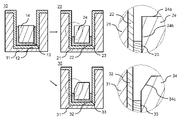
- FIG. 1 is a schematic diagram of an etching process for a semiconductor substrate for memory elements.
- a memory element semiconductor substrate (before etching) 10 has a silicon substrate 11 having a recess, an insulating film 12 made of silicon dioxide, a barrier film (before etching) made of titanium nitride 13 , and a metal tungsten film 14 .
- Such a memory element semiconductor substrate (before etching) 10 is obtained by successively forming an insulating film made of silicon dioxide, a barrier film made of titanium nitride, and a metal tungsten film on a silicon substrate having recesses, followed by CMP (chemical mechanical etching).
- both the barrier film and the metal tungsten film are selectively etched by dry etching, but only the metal tungsten film is selectively etched by dry etching. It can also be configured as
- a semiconductor substrate for memory elements (after etching) 20 By applying an etching composition for a semiconductor substrate for memory elements to a semiconductor substrate for memory elements (before etching) 10, a semiconductor substrate for memory elements (after etching) 20 can be obtained. Specifically, when the etching composition for the semiconductor substrate for memory elements (before etching) is applied to the semiconductor substrate for memory elements (before etching) 10 , the barrier film (before etching) 13 made of titanium nitride is selectively etched and nitrided. A barrier film 23 made of titanium is formed. On the other hand, the metal tungsten film 14 is not etched (corroded), or hardly etched (corroded), and becomes a metal tungsten film 24 .
- the semiconductor substrate for memory devices (after etching) 20 as described above cannot be obtained, and the semiconductor substrate for memory devices (after etching) 30 is obtained.
- the etching composition for the semiconductor substrate for memory elements is applied to the semiconductor substrate for memory elements (before etching) 10
- the barrier film (before etching) 13 made of titanium nitride is etched and the metal tungsten film 14 is also etched. (corrosion) can progress.
- the tungsten metal film 34 of the memory device semiconductor substrate (after etching) 30 has a tungsten metal film corroded surface 34c. Desired physical properties may not be obtained for a memory device manufactured using the memory device semiconductor substrate (after etching) 30 in which the metal tungsten film is corroded.
- the cause of the progression of etching (corrosion) of the metal tungsten film described above is not necessarily clear, for example, the following reasons are conceivable. That is, conventional etching compositions for semiconductor substrates for memory devices usually contain a metal tungsten corrosion inhibitor. Therefore, it is considered that the barrier film (before etching) 13 made of titanium nitride can be selectively etched without etching (corroding) the metal tungsten film 14 . However, as the selective etching of the barrier films 13 and 23 made of titanium nitride progresses, the metal tungsten film side surface 24b is exposed accordingly.
- a narrow gap (for example, about 1 to 5 nm) is formed between the metal tungsten film side surface 24b, the insulating film 22 surface and the barrier film 23 upper surface.
- the metal tungsten corrosion inhibitor which has a relatively small molecular size and which is involved in etching, has a larger molecular size than the oxidizing agent and fluorine compound, and is difficult to enter the above gap. That is, in this gap, since the concentration of the metallic tungsten anticorrosive is relatively lower than the concentrations of the oxidizing agent and the fluorine compound, the anti-etching function of the metallic tungsten anticorrosive contained in the etching composition is exhibited.
- etching (corrosion) of the metal tungsten film side surface 24b may progress. In this way, etching (corrosion) from the direction of the metal tungsten film side surface 24b occurs, so that the metal tungsten film 34 of the memory element semiconductor substrate (after etching) 30 has a slope-shaped metal tungsten film corroded surface 34c. guessed. That is, although the conventional etching composition for semiconductor substrates for memory devices can suppress or prevent etching (corrosion) from the direction of the metal tungsten film surface 24a due to the contained metal tungsten anticorrosive agent, the barrier film 13 made of titanium nitride is not used. In some cases, etching (corrosion) from the direction of the metal tungsten film side surface 24b, which is exposed due to the selective etching of , cannot be sufficiently prevented.
- the etching composition for a semiconductor substrate for a memory element according to the present invention contains a predetermined anticorrosive agent for tungsten metal, so that etching (corrosion) not only from the direction of the tungsten metal film surface 24a but also from the side surface of the tungsten metal film is performed. Etching (corrosion) from the 24b direction can be prevented.
- the predetermined metallic tungsten anticorrosive agent is applied faster than etching (corrosion) occurs on the metallic tungsten film side surface 24b exposed as the selective etching of the barrier film 13 made of titanium nitride proceeds. Absorbable. As a result, it is possible to manufacture a semiconductor substrate for a memory device that has no or almost no metallic tungsten film corroded surface 34c.
- titanium alloy means a material having metallic properties obtained by adding one or more metal elements or non-metal elements other than titanium to titanium.
- the content of the titanium element in the titanium alloy is 20 atomic weight % or more, preferably 30 atomic weight % or more, more preferably 35 atomic weight % or more, and still more preferably 40 to 99.9 based on the total atomic weight of the titanium alloy. atomic weight %.
- Elements other than titanium that can be contained in titanium alloys include aluminum, oxygen, nitrogen, carbon, molybdenum, vanadium, niobium, iron, chromium, nickel, tin, hafnium, zirconium, palladium, ruthenium, and platinum. These elements other than titanium may be contained singly or in combination of two or more in the titanium alloy.
- the oxidizing agent has the function of changing the oxidation number of titanium in titanium and titanium alloys to tetravalent.
- the oxidizing agent is not particularly limited, but includes peracids, halogen oxoacids, and salts thereof.
- peracid examples include hydrogen peroxide, persulfuric acid, percarbonic acid, superphosphoric acid, peracetic acid, perbenzoic acid, and meta-chloroperbenzoic acid.
- halogen oxoacid examples include chlorine oxoacids such as hypochlorous acid, chlorous acid, chloric acid and perchloric acid; oxoacids of iodine such as hypoiodous acid, iodous acid, iodic acid, and periodic acid;
- the salts include alkali metal salts such as lithium salt, sodium salt, potassium salt, rubidium salt and cesium salt of the above peracid or halogen oxoacid; beryllium salt, magnesium salt and calcium salt of the above peracid or halogen oxoacid; alkaline earth metal salts such as strontium salts and barium salts; metal salts such as aluminum salts, copper salts, zinc salts and silver salts of the above peracids or halogen oxoacids; and ammonium salts of the above peracids or halogen oxoacids. be done.
- alkali metal salts such as lithium salt, sodium salt, potassium salt, rubidium salt and cesium salt of the above peracid or halogen oxoacid
- beryllium salt, magnesium salt and calcium salt of the above peracid or halogen oxoacid alkaline earth metal salts such as strontium salts and barium salts
- the above-mentioned (A) oxidizing agent is preferably hydrogen peroxide or an oxoacid of iodine, more preferably hydrogen peroxide, iodic acid or periodic acid, and iodic acid or periodic acid. is more preferred, and iodic acid is particularly preferred from the viewpoint of increasing the Ti/W etching selectivity (etching amount of titanium/titanium alloy/etching amount (corrosion amount) of metallic tungsten).
- the above (A) oxidizing agent may be used alone or in combination of two or more. That is, in one embodiment, the oxidizing agent (A) preferably contains at least one selected from the group consisting of peracids, halogen oxoacids, and salts thereof, and hydrogen peroxide and iodine oxoacids More preferably, at least one selected from the group consisting of hydrogen peroxide, iodic acid, more preferably at least one selected from the group consisting of periodic acid, iodic acid, from periodic acid It is particularly preferred to contain at least one selected from the group consisting of, most preferably periodic acid.
- the addition rate of the oxidizing agent is preferably 0.0001 to 10% by mass, more preferably 0.001 to 5% by mass, relative to the total mass of the etching composition for the semiconductor substrate for memory elements. It is more preferably 0.003 to 3% by mass, and particularly preferably 0.01 to 2% by mass.
- the fluorine compound has a function of promoting etching of titanium and titanium alloys converted to tetravalent.
- the (B) fluorine compound is not particularly limited, but hydrogen fluoride (HF), tetrafluoroboric acid (HBF 4 ), hexafluorosilicic acid (H 2 SiF 6 ), hexafluorozirconic acid (H 2 ZrF 6 ), hexafluorotitanic acid (H 2 TiF 6 ), hexafluorophosphoric acid (HPF 6 ), hexafluoroaluminic acid (H 2 AlF 6 ), hexafluorogermanic acid (H 2 GeF 6 ), and salts thereof. be done.
- the salts include ammonium fluoride (NH 4 F), acidic ammonium fluoride (NH 4 F.HF), ammonium tetrafluoroborate (NH 4 BF 4 ), ammonium hexafluorosilicate ((NH 4 ) 2 SiF 6 ), and ammonium salts such as tetramethylammonium tetrafluoroborate (N(CH 3 ) 4 BF 4 ).
- the fluorine compound (B) is preferably hydrogen fluoride (HF), tetrafluoroboric acid (HBF 4 ), hexafluorosilicic acid (H 2 SiF 6 ), and salts thereof.
- Hydrogen (HF), ammonium fluoride (NH 4 F), acidic ammonium fluoride (NH 4 F.HF), and hexafluorosilicic acid (H 2 SiF 6 ) are more preferable, and prevent corrosion of metallic tungsten.
- Ammonium acid fluoride (NH 4 F.HF) and hexafluorosilicic acid (H 2 SiF 6 ) are more preferable, and hexafluorosilicic acid is more preferable from the viewpoint that the Ti/W etching selectivity can be made higher. (H 2 SiF 6 ) is particularly preferred.
- the above-mentioned (B) fluorine compound may be used individually, or may be used in combination of 2 or more types. That is, in a preferred embodiment, (B) the fluorine compound is hydrogen fluoride (HF), tetrafluoroboric acid (HBF 4 ), hexafluorosilicic acid (H 2 SiF 6 ), hexafluorozirconic acid (H 2 ZrF 6 ), hexafluorotitanic acid (H 2 TiF 6 ), hexafluorophosphoric acid (HPF 6 ), hexafluoroaluminic acid (H 2 AlF 6 ), hexafluorogermanic acid (H 2 GeF 6 ), and salts thereof preferably contains at least one selected from the group consisting of hydrogen fluoride (HF), tetrafluoroboric acid ( HBF4 ), hexafluorosilicic acid ( H2SiF6 ), and salts thereof More preferably, it contains
- the addition rate of the fluorine compound is preferably 0.005 to 10% by mass, more preferably 0.01 to 3% by mass, with respect to the total mass of the etching composition for the semiconductor substrate for memory elements. It is more preferably 0.01 to 1% by mass, and particularly preferably 0.03 to 0.5% by mass.
- the metallic tungsten anticorrosive has the function of quickly adsorbing not only to the normal metallic tungsten but also to the side surface of the metallic tungsten exposed during etching of the adjacent titanium-containing film containing titanium and/or titanium alloys. As a result, the reactivity of the side surfaces of the tungsten metal can be reduced, and etching (corrosion) from the side surfaces of the tungsten metal can be suitably prevented or suppressed.
- the (C) metal tungsten corrosion inhibitor is not particularly limited, but is selected from the group consisting of ammonium salts represented by the following formula (1) and heteroaryl salts having a substituted or unsubstituted alkyl group having 14 to 30 carbon atoms. including at least one
- R 1 is a substituted or unsubstituted alkyl group having 14 to 30 carbon atoms, a substituted or unsubstituted alkyl (poly)heteroalkylene group having 14 to 30 carbon atoms, or a substituted Alternatively, it is an unsubstituted aryl(poly)heteroalkylene group.
- the alkyl group having 14 to 30 carbon atoms is not particularly limited, but is tetradecyl, pentadecyl, hexadecyl, heptadecyl, octadecyl, nonadecyl, icosyl, docosyl, tetracosyl, hexacosyl, octacosyl, and triacontyl. and the like.
- the substituent is not particularly limited, but is fluorine atom, chlorine atom, bromine atom, iodine atom.
- halogen atoms such as atoms; aryl groups having 6 to 20 carbon atoms such as phenyl group and naphthyl group; alkoxy groups having 1 to 6 carbon atoms such as methoxy group, ethoxy group and propyloxy group; hydroxy group; cyano group; nitro group etc.
- the number of substituents may be one, or two or more may be provided.
- a substituted alkyl group having 14 to 30 carbon atoms means that the total number of carbon atoms in the substituent and in the alkyl group is 14 to 30. That is, in the case of a substituted alkyl group having 14 to 30 carbon atoms, depending on the number of carbon atoms in the substituent, the alkyl group has 14 or less carbon atoms (e.g., octyl, decyl, dodecyl, etc.). 8 to 13 alkyl groups).
- An alkyl(poly)heteroalkylene group having 14 to 30 carbon atoms is represented by -(C n H 2n -Z-) m -R 3 .
- each n is independently 1 to 5, preferably 1 to 3, more preferably 1 to 2.
- m is 1-5, preferably 1-2.
- Each Z is independently an oxygen atom (O), a sulfur atom (S) or a phosphorus atom (P), preferably an oxygen atom (O).
- R 3 is an alkyl group having 1 to 30 carbon atoms, such as methyl group, ethyl group, propyl group, isopropyl group, butyl group, pentyl group, hexyl group, heptyl group, octyl group, nonyl group, decyl group, undecyl group, dodecyl group, tridecyl group, tetradecyl group, pentadecyl group, hexadecyl group, heptadecyl group, octadecyl group, nonadecyl group, icosyl group and the like.
- a substituted or unsubstituted alkyl(poly)heteroalkylene group having 14 to 30 carbon atoms has a substituent (substituted alkyl(poly)heteroalkylene group having 14 to 30 carbon atoms)
- the substituent is not particularly limited, halogen atoms such as fluorine atom, chlorine atom, bromine atom and iodine atom; aryl groups having 6 to 20 carbon atoms such as phenyl group and naphthyl group; alkoxy groups having 1 to 6 carbon atoms such as methoxy group, ethoxy group and propyloxy group group; hydroxy group; cyano group; nitro group and the like.
- the said substituent is usually replaced with the hydrogen atom of R3.
- the number of substituents may be one, or two or more may be provided.
- a substituted alkyl(poly)heteroalkylene group having 14 to 30 carbon atoms means that the total number of carbon atoms in the substituent and in the alkyl(poly)heteroalkylene group is 14 to 30.
- the alkyl(poly)heteroalkylene group having 14 to 30 carbon atoms in the case of a substituted alkyl(poly)heteroalkylene group having 14 to 30 carbon atoms, the alkyl(poly)heteroalkylene group having 14 or less carbon atoms (for example, an octyl group , a decyl group, a dodecyl group, or other alkyl group having 8 to 13 carbon atoms).
- An aryl(poly)heteroalkylene group having 14 to 30 carbon atoms is represented by -(C n H 2n -Z-) m -Ar.
- each n is independently 1 to 5, preferably 1 to 3, more preferably 1 to 2.
- m is 1-5, preferably 1-2.
- Each Z is independently an oxygen atom (O), a sulfur atom (S) or a phosphorus atom (P), preferably an oxygen atom (O).
- Ar is an aryl group having 6 to 18 carbon atoms, such as a phenyl group, a naphthyl group and an anthracenyl group.
- the substituent is not particularly limited, halogen atoms such as fluorine atom, chlorine atom, bromine atom and iodine atom; methyl group, ethyl group, propyl group, isopropyl group, butyl group, 1,1-dimethylbutyl group, 2,2-dimethylbutyl group, 1,1 , 3,3-tetramethylbutyl group and other C 1-10 alkyl groups; methoxy, ethoxy, propyloxy and other C 1-6 alkoxy groups; hydroxy groups; cyano groups; mentioned.
- the substituent is usually substituted with a hydrogen atom of Ar.
- the number of substituents may be one, or two or more may be provided.
- a substituted aryl(poly)heteroalkylene group having 14 to 30 carbon atoms means that the total number of carbon atoms in the substituent and in the aryl(poly)heteroalkylene group is 14 to 30.
- the aryl(poly)heteroalkylene group having 14 or less carbon atoms e.g., octyl group , a decyl group, a dodecyl group, or other alkyl group having 8 to 13 carbon atoms.
- R 1 is preferably a substituted or unsubstituted alkyl(poly)heteroalkylene group having 14 to 30 carbon atoms or a substituted or unsubstituted aryl(poly)heteroalkylene group having 14 to 30 carbon atoms.
- a substituted or unsubstituted aryl (poly)heteroalkylene group having 14 to 20 carbon atoms more preferably a substituted or unsubstituted aryl (poly)heteroalkylene group having 16 to 20 carbon atoms
- a substituted or unsubstituted aryl(poly)heteroalkylene group having a number of 18 to 20 is particularly preferred, and p-(1,1,3,3-tetramethylbutyl)phenyldi(oxyethylene) (p-CH 3 C ( Most preferably it is a CH 3 ) 2 CH 2 C(CH 3 ) 2 -Ph-(O-C 2 H 4 ) 2 -) group.
- R 1 is preferably a substituted or unsubstituted alkyl group having 14 to 25 carbon atoms or a substituted or unsubstituted aryl(poly)heteroalkylene group having 14 to 25 carbon atoms.
- a substituted or unsubstituted alkyl group having 14 to 20 carbon atoms a substituted or unsubstituted aryl (poly)heteroalkylene group having 14 to 20 carbon atoms, a tetradecyl group, a hexadecyl group, an octadecyl group, p-(1, 1,3,3-tetramethylbutyl)phenyldi(oxyethylene)(p-CH 3 C(CH 3 ) 2 CH 2 C(CH 3 ) 2 -Ph-(O-C 2 H 4 ) 2 -) group hexadecyl group, octadecyl group, p-(1,1,3,3-tetramethylbutyl)phenyldi(oxyethylene)(p-CH 3 C(CH 3 ) 2 CH 2 C(CH 3 ) 2 -Ph-(O-C 2 H 4 ) 2- ) group is particularly preferred, and
- Each R 2 is independently a substituted or unsubstituted alkyl group having 1 to 30 carbon atoms or a substituted or unsubstituted aryl group having 6 to 30 carbon atoms.
- the alkyl group having 1 to 30 carbon atoms is not particularly limited, but is methyl group, ethyl group, propyl group, isopropyl group, butyl group, isobutyl group, sec-butyl group, tert-butyl group, pentyl group, hexyl group, heptyl group, octyl group, nonyl group, decyl group, dodecyl group, tetradecyl group, hexadecyl group, octadecyl group, nonadecyl group, icosyl group and the like.
- the substituent may be a halogen atom such as a fluorine atom, a chlorine atom, a bromine atom or an iodine atom.
- an aryl group having 6 to 20 carbon atoms such as a phenyl group and a naphthyl group
- an alkoxy group having 1 to 6 carbon atoms such as a methoxy group, an ethoxy group and a propyloxy group
- a hydroxy group such as a cyano group
- the number of substituents may be one, or two or more may be provided.
- a substituted alkyl group having 1 to 30 carbon atoms means that the total number of carbon atoms in the substituent and the total number of carbon atoms in the alkyl group is 1 to 30.
- the aryl group having 6 to 30 carbon atoms is not particularly limited, but includes phenyl group, naphthyl group, biphenyl group and the like.
- the substituent may be a halogen atom such as a fluorine atom, a chlorine atom, a bromine atom or an iodine atom.
- Alkyl groups having 1 to 10 carbon atoms such as methyl group, ethyl group, propyl group and isopropyl group; Alkoxy groups having 1 to 6 carbon atoms such as methoxy group, ethoxy group and propyloxy group; Hydroxy group; Cyano group; Nitro and the like.
- the number of substituents may be one, or two or more may be provided.
- a substituted aryl group having 6 to 30 carbon atoms means that the total number of carbon atoms in the substituent and the total number of carbon atoms in the alkyl group is 6 to 30.
- R 2 is preferably a substituted or unsubstituted alkyl group having 1 to 30 carbon atoms, such as methyl group, ethyl group, propyl group, isopropyl group, hexyl group, octyl group, decyl group, dodecyl group, A tetradecyl group, a hexadecyl group, an octadecyl group, a benzyl group, a hydroxymethyl group, and a 2-hydroxyethyl group are more preferable, and a methyl group, an ethyl group, a benzyl group, and a 2-hydroxyethyl group are more preferable, and methyl A benzyl group is particularly preferred, and a methyl group is most preferred.
- R 2 is preferably an alkyl group having 1 to 10 carbon atoms substituted with an aryl group having 6 to 20 carbon atoms, and is more preferably an alkyl group of, more preferably a benzyl group or a phenylethyl group, and particularly preferably a benzyl group.
- X is halide ion (fluoride ion, chloride ion, bromide ion, iodide ion, etc.), hydroxide ion, organic sulfonate ion (methanesulfonate ion, p-toluenesulfonate ion, etc.), tetrafluoro borate anion, hexafluorophosphate anion.
- X is preferably a halide ion, more preferably a chloride ion or a bromide ion.
- ammonium salt represented by formula (1) wherein R 1 is a substituted or unsubstituted alkyl group having 14 to 30 carbon atoms, include tetradecyl groups such as tetradecyltrimethylammonium bromide and benzyldimethyltetradecylammonium chloride.
- hexadecyltrimethylammonium chloride hexadecyltrimethylammonium bromide, hexadecyltrimethylammonium p-toluenesulfonate, hexadecyltrimethylammonium hydroxide, ethylhexadecyldimethylammonium chloride, ethylhexadecyldimethylammonium bromide, benzyldimethylhexadecyl ammonium salts having a hexadecyl group such as ammonium chloride; and ammonium salts having an octadecyl group such as trimethyloctadecyl ammonium chloride, trimethyloctadecylammonium bromide, dimethyldioctadecylammonium chloride, dimethyldioctadecylammonium bromide, benzyldi
- ammonium salt represented by Formula (1) wherein R 1 is a substituted or unsubstituted alkyl(poly)heteroalkylene group having 14 to 30 carbon atoms, include trimethylpropyldi(oxyethylene)ammonium chloride, trimethylpropyl oxyethylenethioethyleneammonium chloride and the like.
- ammonium salt represented by formula (1) wherein R 1 is a substituted or unsubstituted aryl(poly)heteroalkylene group having 14 to 30 carbon atoms, include benzyldimethyl-2- ⁇ 2-[4-( 1,1,3,3-tetramethylbutyl)phenoxy]ethoxy ⁇ ethylammonium chloride (benzethonium chloride), benzyldimethylphenyldi(oxyethylene)ammonium chloride and the like.
- heteroaryl salt having a substituted or unsubstituted alkyl group having 14 to 30 carbon atoms is not particularly limited, but at least one of the nitrogen atoms of the substituted or unsubstituted nitrogen atom-containing heteroaryl ring has 14 carbon atoms. Salts of heteroaryl cations with ⁇ 30 substituted or unsubstituted alkyl groups are included.
- the nitrogen atom-containing heteroaryl ring is not particularly limited, but includes rings such as imidazole, pyrazole, oxazole, isoxazole (isoxazole), thiazole, isothiazole, pyridine, pyrazine, pyridazine, pyrimidine, quinoline, and isoquinoline.
- the alkyl group having 14 to 30 carbon atoms is not particularly limited, but is tetradecyl, pentadecyl, hexadecyl, heptadecyl, octadecyl, nonadecyl, icosyl, docosyl, tetracosyl, hexacosyl, octacosyl, and triacontyl. and the like.
- the substituent may be a halogen atom such as a fluorine atom, a chlorine atom, a bromine atom or an iodine atom.
- Alkyl groups having 1 to 4 carbon atoms such as methyl group, ethyl group, propyl group and isopropyl group; Aryl groups having 6 to 20 carbon atoms such as phenyl group and naphthyl group; Methoxy group, ethoxy group and propyloxy group alkoxy groups having 1 to 6 carbon atoms; hydroxy groups; cyano groups; and nitro groups.
- the number of substituents may be one, or two or more may be provided.
- a substituted alkyl group having 14 to 30 carbon atoms means that the total number of carbon atoms in the substituent and in the alkyl group is 14 to 30.
- the alkyl group has 14 or less carbon atoms (e.g., octyl, decyl, dodecyl, etc.). 8 to 13 alkyl groups).
- the substituted or unsubstituted alkyl group having 14 to 30 carbon atoms is preferably a substituted or unsubstituted alkyl group having 14 to 20 carbon atoms, more preferably an alkyl group having 14 to 20 carbon atoms.
- tetradecyl group, hexadecyl group and octadecyl group are more preferred, and hexadecyl group and octadecyl group are particularly preferred.
- the counter anion of the heteroaryl cation having a substituted or unsubstituted alkyl group having 14 to 30 carbon atoms is not particularly limited, but halide ions such as fluoride ion, chloride ion, bromide ion and iodide ion; hydroxide ion; organic sulfonate ions such as methanesulfonate ion and p-toluenesulfonate ion; tetrafluoroborate anion; hexafluorophosphate anion and the like.
- the counter anion is preferably a halide ion, more preferably a chloride ion or a bromide ion.
- heteroaryl salts having a substituted or unsubstituted alkyl group having 14 to 30 carbon atoms include 1-tetradecyl-3-methylimidazolium chloride, 1-tetradecyl-3-methylimidazolium bromide, 1-hexadecyl-3 - imidazolium salts such as methylimidazolium chloride, 1-hexadecyl-3-methylimidazolium bromide, 1-octadecyl-3-methylimidazolium chloride, 1-octadecyl-3-methylimidazolium bromide; 3-tetradecyloxazolium chloride oxazolium salts such as , 3-hexadecyloxazolium chloride and 3-octadecyloxazolium chloride; thiazolium such as 3-tetradecylthiazolium chloride, 3-hexadecylthiazolium chloride and 3-octa
- the metal tungsten anticorrosive agent is preferably an ammonium salt represented by formula (1) from the viewpoint of increasing the Ti/W etching selectivity.
- ammonium salt (here, R 1 is a substituted or unsubstituted alkyl group having 15 to 20 carbon atoms, a substituted or unsubstituted alkyl (poly)heteroalkylene group having 15 to 20 carbon atoms, or a substituted or unsubstituted aryl(poly)heteroalkylene group), and an ammonium salt represented by formula (1) (wherein R 1 is an alkyl group having 17 to 20 carbon atoms; 17 to 20 substituted aryl (poly)heteroalkylene group) is more preferable, and an ammonium salt represented by formula (1) (wherein R 1 is a substituted aryl (poly) having 17 to 20 carbon atoms (poly ) is a heteroalkylene group), and most preferably benzethonium chlor
- the above-mentioned (C) metal tungsten corrosion inhibitor may be used individually, or may be used in combination of 2 or more types. That is, in a preferred embodiment, (C) the metal tungsten anticorrosive agent preferably contains at least one ammonium salt represented by formula (1), and the ammonium salt represented by formula (1) (where , R 1 is a substituted or unsubstituted alkyl group having 15 to 20 carbon atoms, a substituted or unsubstituted alkyl (poly)heteroalkylene group having 15 to 20 carbon atoms, or a substituted or unsubstituted aryl (poly) group having 15 to 20 carbon atoms.
- R 1 is a substituted or unsubstituted alkyl group having 15 to 20 carbon atoms, a substituted or unsubstituted alkyl (poly)heteroalkylene group having 15 to 20 carbon atoms, or a substituted or unsubstituted aryl (pol
- R 1 is an alkyl group having 17 to 20 carbon atoms, 17 to 20 carbon atoms is a substituted aryl (poly)heteroalkylene group), and an ammonium salt represented by formula (1) (wherein R 1 is a substituted aryl having 17 to 20 carbon atoms ( poly)heteroalkylene groups), and most preferably at least one of benzethonium chloride and benzethonium bromide.
- the addition rate of the metal tungsten anticorrosive agent is preferably 0.0001 to 5% by mass, more preferably 0.001 to 1% by mass, based on the total mass of the etching composition for the semiconductor substrate for memory elements. is more preferable, 0.003 to 0.5% by mass is more preferable, and 0.004 to 0.08% by mass is particularly preferable.
- the etching composition for semiconductor substrates for memory devices may contain (D) a pH adjuster, if necessary.
- the etching composition for semiconductor substrates for memory devices preferably further includes (D) a pH adjuster.
- (D) pH adjuster for example, (A) an oxidizing agent, (B) an acid or an alkali other than a fluorine compound can be used.
- the acid examples include hydrogen chloride, hydrogen bromide, hydrogen iodide, sulfuric acid, nitric acid, methanesulfonic acid, trifluoromethanesulfonic acid, benzenesulfonic acid, p-toluenesulfonic acid, 10-camphorsulfonic acid, and salts thereof.
- the salt includes ammonium salts such as ammonium chloride, ammonium bromide, ammonium iodide, ammonium sulfate, and ammonium nitrate; methylamine hydrochloride, dimethylamine hydrochloride, dimethylamine hydrobromide, methylamine sulfate, etc. and alkylammonium salts of.
- alkali examples include lithium hydroxide, sodium hydroxide, potassium hydroxide, rubidium hydroxide, cesium hydroxide, beryllium hydroxide, magnesium hydroxide, calcium hydroxide, strontium hydroxide, barium hydroxide, ammonia, triethylamine, and the like. mentioned.
- the (D) pH adjuster is preferably hydrogen chloride, hydrogen bromide, hydrogen iodide, sulfuric acid, nitric acid, methanesulfonic acid, or ammonia, and is preferably hydrogen chloride, sulfuric acid, or methanesulfonic acid.
- Hydrogen chloride and methanesulfonic acid are more preferable, and methanesulfonic acid is particularly preferable, from the viewpoints of preventing corrosion of metal tungsten and increasing the Ti/W etching selectivity.
- the above-mentioned (D) pH adjuster may be used alone or in combination of two or more. That is, in a preferred embodiment, (D) the pH adjuster contains at least one selected from the group consisting of hydrogen chloride, hydrogen bromide, hydrogen iodide, sulfuric acid, nitric acid, methanesulfonic acid, and ammonia. is preferred, more preferably contains at least one selected from the group consisting of hydrogen chloride, sulfuric acid, and methanesulfonic acid, and further contains at least one selected from the group consisting of hydrogen chloride and methanesulfonic acid Preferably, methanesulfonic acid is particularly preferred.
- the addition rate of the pH adjuster varies depending on the pH of the etching composition for semiconductor substrates for memory elements before adjustment, but is 0.0001 to 0.0001 with respect to the total mass of the etching composition for semiconductor substrates for memory elements. It is preferably 5% by mass, more preferably 0.01 to 3% by mass, even more preferably 0.1 to 1% by mass, and 0.3 to 0.75% by mass. Especially preferred.
- the etching composition for semiconductor substrates for memory devices preferably contains water.
- the water has a function of uniformly dispersing each component contained in the etching composition for the semiconductor substrate for memory devices, a function of diluting the composition, and the like.
- the water is not particularly limited, but it is preferably water from which metal ions, organic impurities, particles, etc. have been removed by distillation, ion exchange treatment, filter treatment, various adsorption treatments, etc. Pure water is preferred. More preferably, ultrapure water is particularly preferred.
- the addition rate of water is preferably 50% by mass or more, more preferably 80% by mass or more, and 90% by mass or more with respect to the total mass of the etching composition for a semiconductor substrate for memory elements. More preferably, it is particularly preferably 90 to 99.5% by mass.
- the etching composition for semiconductor substrates for memory devices may optionally contain (E) an organic solvent.
- the etching composition for semiconductor substrates for memory devices preferably further includes (E) an organic solvent.
- the organic solvent further lowers the surface tension of the etching composition for the semiconductor substrate for memory devices, thereby reducing the metal content generated as the selective etching of the titanium-containing film (barrier film) containing titanium and titanium alloy proceeds. It is believed that the metallic tungsten anticorrosive agent can easily enter into the fine spaces on the side surfaces of the tungsten film, and has the function of suitably preventing or suppressing etching (corrosion) from the side surfaces of the metallic tungsten film.
- the (E) organic solvent is not particularly limited, but monoalcohols (methanol, ethanol, 1-propanol, 2-propanol, 1-butanol, tert-butanol, 1-pentanol, 1-hexanol, 1-heptanol , 1-octanol, 1-nonanol, 1-decanol, etc.), diols (ethylene glycol, propylene glycol, neopentyl glycol, 1,2-hexanediol, 1,6-hexanediol, 2-ethylhexane-1,3- diols, etc.), polyhydric alcohols (glycerin, etc.); ethers such as dimethyl ether, diethyl ether, tetrahydrofuran, 1,4-dioxane; diethylene glycol monomethyl ether, diethylene glycol monoethyl ether, diethylene glycol monobutyl ether, propylene glycol mono
- the (E) organic solvent has a high boiling point and is preferably an alcohol, more preferably a monoalcohol or a diol, from the viewpoint of stability, 1-hexanol, 1-heptanol, More preferably, 1-octanol, 1-nonanol, 1-decanol, 1,2-hexanediol, 1,6-hexanediol, 2-ethylhexane-1,3-diol, 1-hexanol, 1- More preferred are butanol, 1-octanol and 2-ethylhexane-1,3-diol, and particularly preferred are 1-hexanol, 1-heptanol and 1-octanol.
- organic solvent may be used alone or in combination of two or more. That is, in a preferred embodiment, (E) the organic solvent preferably contains at least one alcohol, more preferably at least one selected from the group consisting of monoalcohols and diols, 1-hexanol , 1-heptanol, 1-octanol, 1-nonanol, 1-decanol, 1,2-hexanediol, 1,6-hexanediol, and 2-ethylhexane-1,3-diol more preferably at least one, particularly preferably at least one selected from the group consisting of 1-hexanol, 1-heptanol, 1-octanol, and 2-ethylhexane-1,3-diol , 1-hexanol, 1-heptanol, and 1-octanol.
- the organic solvent preferably contains at least one alcohol, more preferably at least one selected from the group consisting of monoalcohols
- the addition rate of the organic solvent varies depending on the composition, surface tension, etc. of the etching composition for semiconductor substrates for memory elements before adjustment. It is preferably 50% by mass or less, more preferably 10% by mass or less, still more preferably 0.01 to 7.5% by mass, and particularly preferably 0.05 to 5% by mass. , 0.5 to 3% by weight.
- the etching composition for a semiconductor substrate for memory devices preferably further contains an iodine scavenger.
- the iodine scavenger is not particularly limited, but acetone, butanone, 2-methyl-2-butanone, 3,3-dimethyl-2-butanone, 4-hydroxy-2-butanone, 2-pentanone, 3-pentanone, 3 -methyl-2-pentanone, 4-methyl-2-pentanone, 2-methyl-3-pentanone, 5-methyl-3-pentanone, 2,4-dimethyl-3-pentanone, 5-hydroxy-2-pentanone, 4 -hydroxy-4-methyl-2-pentanone, 2-hexanone, 3-hexanone, 2-heptanone, 3-heptanone, 4-heptanone, 5-methyl-2-heptanone, 5-methyl-3-heptanone, 2,6 -aliphatic ketones such as dimethyl-4-heptanone, 2-octanone, 3-octanone, 4-octanone, cyclohexanone, 2,6-dimethylcyclohexanone, 2-acetyl
- the etching composition for semiconductor substrates for memory devices may further comprise a low dielectric passivator.
- a low dielectric constant passivating agent has a function of preventing or suppressing etching of a low dielectric constant film such as an insulating film.
- low dielectric constant passivating agent examples include, but are not limited to, boric acid; borates such as ammonium pentaborate and sodium tetraborate; carboxylic acids such as 3-hydroxy-2-naphthoic acid, malonic acid and iminodiacetic acid. mentioned.
- These low dielectric constant passivating agents may be used alone or in combination of two or more.
- the addition rate of the low dielectric constant passivating agent is preferably 0.01 to 2% by mass, more preferably 0.02 to 1% by mass, based on the total mass of the etching composition for semiconductor substrates for memory devices. is more preferable, and 0.03 to 0.5% by mass is even more preferable.
- the etching composition for semiconductor substrates for memory devices may further contain additives.
- additives include surfactants, chelating agents, antifoaming agents, silicon-containing compounds, and the like.
- the surface tension of the etching composition for semiconductor substrates for memory devices is preferably 50 mN/m or less, more preferably 40 mN/m or less, even more preferably 10 to 35 mN/m, further preferably 20 to 32 mN. /m is particularly preferred, and 25-30 mN/m is most preferred.
- the surface tension of the etching composition for semiconductor substrates for memory elements is 50 mN/m or less, fine grains on the side surfaces of the metallic tungsten film are generated as the selective etching of the titanium-containing film (barrier film) containing titanium and titanium alloy progresses.
- the metal tungsten anticorrosive agent can easily enter into the space where the metal tungsten is exposed, and etching (corrosion) from the side surface of the metal tungsten can be suitably prevented or suppressed.
- the surface tension is measured by the method described in Examples.
- the surface tension of the etching composition for the semiconductor substrate for memory elements can be adjusted by, for example, using (C) a metal tungsten anticorrosive agent with a higher number of carbon atoms, or adding a (E) organic solvent with a higher hydrophobicity. can be done.
- the pH of the etching composition for semiconductor substrates for memory devices is preferably 0.1 to 5.0, more preferably 0.5 to 3.0, and 0.8 to 1.5. is more preferred, and 0.8 to 1.3 is particularly preferred. It is preferable that the pH of the etching composition for semiconductor substrates for memory elements is within the above range, since the amount of etching (corrosion) of metallic tungsten can be reduced. In addition, in this specification, pH is measured by the method as described in an Example. Further, the pH of the etching composition for the semiconductor substrate for memory elements can be adjusted by, for example, adding (D) a pH adjuster.
- a method of manufacturing a semiconductor substrate for a memory device includes contacting a semiconductor substrate having a titanium-containing film containing at least one of titanium and a titanium alloy and a metallic tungsten film with the above etching composition for a semiconductor substrate for memory elements to remove the titanium.
- the step of removing at least a portion of the containing film is included.
- the semiconductor substrate has a titanium-containing film, including at least one of titanium and titanium alloys, and a metallic tungsten film.
- the configuration of the semiconductor substrate is not particularly limited, and a known configuration can be employed as appropriate.
- the semiconductor substrate when used for embedded word lines of memory elements, has a structure in which an insulating film, a barrier film made of titanium and/or a titanium alloy, and a metal tungsten film are laminated in this order on a silicon substrate having a recess. can have At this time, the barrier film and the metal tungsten film are usually arranged adjacent to each other.
- etching composition for semiconductor substrate for memory device As the etching composition for the semiconductor substrate for memory devices, the above-mentioned composition is used.
- the method of contacting the semiconductor substrate with the etching composition for the semiconductor substrate for memory devices is not particularly limited, and known techniques can be appropriately employed.
- the semiconductor substrate may be immersed in the etching composition for the semiconductor substrate for memory elements, the semiconductor substrate may be sprayed with the etching composition for the semiconductor substrate for memory elements, or the semiconductor substrate may be dripped (single-wafer spinning). processing, etc.).
- the immersion may be repeated two or more times
- the spraying may be repeated two or more times
- the dropping may be repeated two or more times
- the immersion, spraying, and dropping may be combined.
- the contact time is not particularly limited, but is preferably 10 seconds to 3 hours, more preferably 30 seconds to 1 hour, even more preferably 1 to 45 minutes, and 1 to 5 minutes. is particularly preferred.
- the obtained semiconductor substrate for memory devices can be used for memory devices such as DRAM.
- the memory element can be made smaller and have higher functionality.
- Example 1 (A) iodic acid (HIO 3 ) as an oxidizing agent, (B) hydrogen fluoride (HF) as a fluorine compound, and (C) metal tungsten (W) and benzethonium chloride (BZT) as an anticorrosive agent.
- HIO 3 iodic acid
- B hydrogen fluoride
- W metal tungsten
- BZT benzethonium chloride
- the addition ratios of iodic acid, hydrogen fluoride, and benzethonium chloride (BZT) are 0.018% by mass, 0.05% by mass, and and 0.02% by mass.
- the pH and surface tension of the etching composition for semiconductor substrates for memory devices were 2.4 and 38 mN/m, respectively.
- the pH of the etching composition for the semiconductor substrate for memory element was measured at 23° C. using a desktop pH meter (F-71) and a pH electrode (9615S-10D) manufactured by Horiba, Ltd.
- the surface tension of the etching composition for the memory element semiconductor substrate was measured at 23° C. using an automatic surface tension meter DY-300 (manufactured by Kyowa Interface Science Co., Ltd.).
- a thermal oxide film (100 nm) made of silicon dioxide was formed on a silicon substrate.
- a titanium nitride film (5 nm), a metal tungsten film (50 nm), and a silicon dioxide film (50 nm) were sequentially formed on the surface of this thermal oxide film by CVD (chemical vapor deposition) to fabricate a wafer.
- An evaluation sample (before etching) was prepared by forming a trench (groove) in the manufactured wafer from the side of the silicon dioxide film formed by CVD to reach the thermal oxide film made of silicon dioxide on the surface of the silicon substrate. did. Specifically, the produced wafer was cut into 1 cm ⁇ 1 cm, and a carbon protective film was formed in a trench (groove) forming region in an FIB (focused ion beam) device (Helios G4 UX (manufactured by Thermo Scientific). Then, a trench (groove) was formed on the wafer from the surface of the carbon protective film by FIB.
- a sample for evaluation (before etching) was prepared by processing at 70° C. for 5 minutes using (prepared by ).
- the evaluation sample (before etching) 40 includes a silicon substrate 41, a thermal oxide film 42 (100 nm) made of silicon dioxide, a titanium nitride film 43 (5 nm), a metal tungsten film 44 (50 nm), a silicon dioxide film 45 (50 nm). ), and a carbon protective film 46 in this order.
- a trench (groove) is formed by FIB from the silicon dioxide film 45 to the thermal oxide film 42 made of silicon dioxide through the carbon protective film 46 .
- the trench (groove) formed has a trapezoidal shape, the width of the trench (groove) at the interface between the silicon dioxide film 45 and the metal tungsten film 44 is 40 nm, and the thermal oxide film made of the titanium nitride film 43 and silicon dioxide is formed.
- the width of the trench at the interface of 42 was 20 nm.
- etching process A sample for evaluation (before etching) was immersed in the etching composition for semiconductor substrates for memory devices and allowed to stand at 50° C. for 30 minutes. The evaluation sample was taken out from the etching composition for the memory element semiconductor substrate and subjected to FIB processing to obtain an evaluation sample having a smooth cross section (after etching).
- FIG. 3 is a schematic diagram of the evaluation sample (after etching).
- the titanium nitride film 53 is etched.
- the metal tungsten film 54 may be etched (corroded).
- the amount of corrosion of the metallic tungsten film was calculated using Image J (image processing software developed by Wayne Rasband of the National Institutes of Health, USA) for the TEM image obtained above. . Specifically, the metal tungsten film corroded region 57 (area) in FIG. 3 was digitized (unit: nm 2 ). The results obtained are shown in Table 2 below.
- TiN/W etching selectivity (Calculation of TiN/W etching selectivity) The TiN/W etching selectivity was calculated by dividing the etching amount (nm 2 ) of the titanium nitride film by the corrosion amount (nm 2 ) of the metallic tungsten film. The results obtained are shown in Table 2 below.
Landscapes
- Chemical & Material Sciences (AREA)
- Engineering & Computer Science (AREA)
- Materials Engineering (AREA)
- Organic Chemistry (AREA)
- Inorganic Chemistry (AREA)
- Manufacturing & Machinery (AREA)
- Chemical Kinetics & Catalysis (AREA)
- General Chemical & Material Sciences (AREA)
- Mechanical Engineering (AREA)
- Metallurgy (AREA)
- Weting (AREA)
- Semiconductor Memories (AREA)
Priority Applications (4)
| Application Number | Priority Date | Filing Date | Title |
|---|---|---|---|
| JP2023532005A JPWO2023277048A1 (https=) | 2021-07-02 | 2022-06-29 | |
| CN202280045082.4A CN117581338A (zh) | 2021-07-02 | 2022-06-29 | 存储元件用半导体基板的蚀刻组合物和使用其的存储元件用半导体基板的制造方法 |
| US18/573,719 US20240287385A1 (en) | 2021-07-02 | 2022-06-29 | Etching composition for semiconductor substrate for memory element and method for manufacturing semiconductor substrate for memory element using same |
| KR1020237042854A KR20240029551A (ko) | 2021-07-02 | 2022-06-29 | 메모리소자용 반도체 기판의 에칭 조성물 및 이것을 이용한 메모리소자용 반도체 기판의 제조방법 |
Applications Claiming Priority (2)
| Application Number | Priority Date | Filing Date | Title |
|---|---|---|---|
| JP2021-110798 | 2021-07-02 | ||
| JP2021110798 | 2021-07-02 |
Publications (1)
| Publication Number | Publication Date |
|---|---|
| WO2023277048A1 true WO2023277048A1 (ja) | 2023-01-05 |
Family
ID=84690245
Family Applications (1)
| Application Number | Title | Priority Date | Filing Date |
|---|---|---|---|
| PCT/JP2022/025880 Ceased WO2023277048A1 (ja) | 2021-07-02 | 2022-06-29 | メモリ素子用半導体基板のエッチング組成物およびこれを用いたメモリ素子用半導体基板の製造方法 |
Country Status (6)
| Country | Link |
|---|---|
| US (1) | US20240287385A1 (https=) |
| JP (1) | JPWO2023277048A1 (https=) |
| KR (1) | KR20240029551A (https=) |
| CN (1) | CN117581338A (https=) |
| TW (1) | TW202311566A (https=) |
| WO (1) | WO2023277048A1 (https=) |
Cited By (1)
| Publication number | Priority date | Publication date | Assignee | Title |
|---|---|---|---|---|
| WO2025127048A1 (ja) * | 2023-12-13 | 2025-06-19 | 三菱瓦斯化学株式会社 | 半導体基板洗浄用組成物、半導体基板の洗浄方法、及び半導体基板の製造方法 |
Citations (2)
| Publication number | Priority date | Publication date | Assignee | Title |
|---|---|---|---|---|
| WO2015111684A1 (ja) * | 2014-01-27 | 2015-07-30 | 三菱瓦斯化学株式会社 | 窒化チタン除去用液体組成物およびそれを用いた半導体素子の洗浄方法、並びに半導体素子の製造方法 |
| JP2016510175A (ja) * | 2013-03-04 | 2016-04-04 | アドバンスド テクノロジー マテリアルズ,インコーポレイテッド | 窒化チタンを選択的にエッチングするための組成物および方法 |
-
2022
- 2022-06-29 CN CN202280045082.4A patent/CN117581338A/zh active Pending
- 2022-06-29 JP JP2023532005A patent/JPWO2023277048A1/ja active Pending
- 2022-06-29 WO PCT/JP2022/025880 patent/WO2023277048A1/ja not_active Ceased
- 2022-06-29 US US18/573,719 patent/US20240287385A1/en active Pending
- 2022-06-29 KR KR1020237042854A patent/KR20240029551A/ko active Pending
- 2022-06-30 TW TW111124419A patent/TW202311566A/zh unknown
Patent Citations (2)
| Publication number | Priority date | Publication date | Assignee | Title |
|---|---|---|---|---|
| JP2016510175A (ja) * | 2013-03-04 | 2016-04-04 | アドバンスド テクノロジー マテリアルズ,インコーポレイテッド | 窒化チタンを選択的にエッチングするための組成物および方法 |
| WO2015111684A1 (ja) * | 2014-01-27 | 2015-07-30 | 三菱瓦斯化学株式会社 | 窒化チタン除去用液体組成物およびそれを用いた半導体素子の洗浄方法、並びに半導体素子の製造方法 |
Cited By (1)
| Publication number | Priority date | Publication date | Assignee | Title |
|---|---|---|---|---|
| WO2025127048A1 (ja) * | 2023-12-13 | 2025-06-19 | 三菱瓦斯化学株式会社 | 半導体基板洗浄用組成物、半導体基板の洗浄方法、及び半導体基板の製造方法 |
Also Published As
| Publication number | Publication date |
|---|---|
| KR20240029551A (ko) | 2024-03-05 |
| TW202311566A (zh) | 2023-03-16 |
| CN117581338A (zh) | 2024-02-20 |
| US20240287385A1 (en) | 2024-08-29 |
| JPWO2023277048A1 (https=) | 2023-01-05 |
Similar Documents
| Publication | Publication Date | Title |
|---|---|---|
| JP6329909B2 (ja) | 窒化チタンを選択的にエッチングするための組成物および方法 | |
| JP2019134168A (ja) | 窒化チタンを選択的にエッチングするための組成物及び方法 | |
| CN116096837B (zh) | 氮化物蚀刻剂组合物和方法 | |
| KR102207306B1 (ko) | 에칭 후 잔류물을 제거하기 위한 세정 조성물 | |
| WO2022172862A1 (ja) | 半導体基板洗浄用組成物、並びに半導体基板の洗浄方法および製造方法 | |
| WO2023277048A1 (ja) | メモリ素子用半導体基板のエッチング組成物およびこれを用いたメモリ素子用半導体基板の製造方法 | |
| JP7827057B2 (ja) | メモリ素子用半導体基板の製造方法 | |
| TW202208597A (zh) | 矽蝕刻液以及使用該矽蝕刻液之矽元件的製造方法及矽基板的處理方法 | |
| US20260022311A1 (en) | Semiconductor substrate cleaning composition, and method for producing semiconductor substrate using same | |
| KR20230122597A (ko) | 실리콘 에칭액, 그 에칭액을 사용한 실리콘 디바이스의 제조 방법 및 기판 처리 방법 | |
| CN116806366A (zh) | 半导体基板清洗用组合物、以及半导体基板的清洗方法和制造方法 | |
| KR102953841B1 (ko) | 실리콘 에칭액, 그리고 그 에칭액을 사용한 실리콘 디바이스의 제조 방법 및 실리콘 기판의 처리 방법 | |
| US12466999B2 (en) | Silicon etching liquid, and method for producing silicon device and method for processing silicon substrate, each using said etching liquid | |
| WO2024004980A1 (ja) | 半導体基板洗浄用組成物、半導体基板の洗浄方法、及び半導体基板の製造方法 | |
| JP2010067982A (ja) | エッチング液 |
Legal Events
| Date | Code | Title | Description |
|---|---|---|---|
| 121 | Ep: the epo has been informed by wipo that ep was designated in this application |
Ref document number: 22833194 Country of ref document: EP Kind code of ref document: A1 |
|
| WWE | Wipo information: entry into national phase |
Ref document number: 2023532005 Country of ref document: JP |
|
| WWE | Wipo information: entry into national phase |
Ref document number: 18573719 Country of ref document: US |
|
| WWE | Wipo information: entry into national phase |
Ref document number: 202280045082.4 Country of ref document: CN |
|
| NENP | Non-entry into the national phase |
Ref country code: DE |
|
| 122 | Ep: pct application non-entry in european phase |
Ref document number: 22833194 Country of ref document: EP Kind code of ref document: A1 |