WO2023248751A1 - 弾性波装置、弾性波装置の製造方法、および通信装置 - Google Patents
弾性波装置、弾性波装置の製造方法、および通信装置 Download PDFInfo
- Publication number
- WO2023248751A1 WO2023248751A1 PCT/JP2023/020401 JP2023020401W WO2023248751A1 WO 2023248751 A1 WO2023248751 A1 WO 2023248751A1 JP 2023020401 W JP2023020401 W JP 2023020401W WO 2023248751 A1 WO2023248751 A1 WO 2023248751A1
- Authority
- WO
- WIPO (PCT)
- Prior art keywords
- layer
- region
- wave device
- electrode layer
- acoustic wave
- Prior art date
- Legal status (The legal status is an assumption and is not a legal conclusion. Google has not performed a legal analysis and makes no representation as to the accuracy of the status listed.)
- Ceased
Links
Images
Classifications
-
- H—ELECTRICITY
- H03—ELECTRONIC CIRCUITRY
- H03H—IMPEDANCE NETWORKS, e.g. RESONANT CIRCUITS; RESONATORS
- H03H3/00—Apparatus or processes specially adapted for the manufacture of impedance networks, resonating circuits, resonators
- H03H3/007—Apparatus or processes specially adapted for the manufacture of impedance networks, resonating circuits, resonators for the manufacture of electromechanical resonators or networks
- H03H3/08—Apparatus or processes specially adapted for the manufacture of impedance networks, resonating circuits, resonators for the manufacture of electromechanical resonators or networks for the manufacture of resonators or networks using surface acoustic waves
-
- H—ELECTRICITY
- H03—ELECTRONIC CIRCUITRY
- H03H—IMPEDANCE NETWORKS, e.g. RESONANT CIRCUITS; RESONATORS
- H03H9/00—Networks comprising electromechanical or electro-acoustic elements; Electromechanical resonators
- H03H9/02—Details
- H03H9/125—Driving means, e.g. electrodes, coils
- H03H9/145—Driving means, e.g. electrodes, coils for networks using surface acoustic waves
Definitions
- the present disclosure relates to an elastic wave device.
- An acoustic wave device includes a piezoelectric layer, an electrode layer located on an upper surface of the piezoelectric layer, an underbump metal, and a bump, and the underbump metal is attached to the piezoelectric layer. It has a first region that is directly bonded and a second region that is bonded to the electrode layer, and when the piezoelectric layer is viewed in plan, at least a portion of the first region and at least a portion of the bump , overlap.
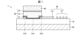
- FIG. 1 is a cross-sectional structural diagram of an elastic wave device according to Embodiment 1 of the present disclosure.
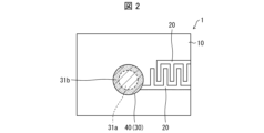
- FIG. 1 is a plan view of an elastic wave device according to Embodiment 1 of the present disclosure.
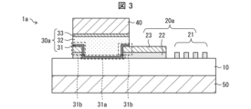
- FIG. 3 is a cross-sectional structural diagram of an elastic wave device according to Embodiment 3 of the present disclosure.
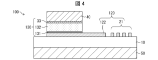
- FIG. 1 is a cross-sectional structural diagram of a general elastic wave device.
- the bump not only has the function of electrically connecting the acoustic wave device and the package, but also has the function of mechanically fixing the acoustic wave device to the package.
- the strength of the bond between the elastic wave device and the bump has not always been sufficient.
- FIG. 4 is a cross-sectional structural diagram of a general acoustic wave device 100.
- the acoustic wave device 100 includes a support substrate 50, a piezoelectric layer 10, an electrode layer 120, an under bump metal 130, and a bump 40, which are overlapped.
- the piezoelectric layer 10 is a thin film made of piezoelectric material.
- the piezoelectric material include LT (lithium tantalate: LiTaO 3 ) and LN (lithium niobate: LiNbO 3 ).
- the piezoelectric layer 10 may be a piezoelectric single crystal such as quartz, or a piezoelectric ceramic such as lead zirconate titanate ceramic. In this embodiment, LT is used.
- Piezoelectric layer 10 is formed on support substrate 50 . Furthermore, the support substrate 50 may have a cavity between it and the piezoelectric layer 10. Between the piezoelectric layer 10 and the support substrate 50 there may be a thin SiO 2 layer or a plurality of low acoustic impedance layers, e.g. SiO 2 and a plurality of high acoustic impedance layers, e.g. HfO 2 . It may have an acoustic reflective film in which these are alternately laminated. Alternatively, the piezoelectric layer 10 may have a sufficient thickness without the support substrate 50.
- the electrode layer 120 includes an IDT electrode section 21 and a pad section 122.
- the electrode layer 20 is generally made of a material containing aluminum, and in this embodiment, the pattern is formed by etching an aluminum alloy (AlCu) film. Further, the electrode layer 120 may be formed using other metals or alloys such as copper (Cu).
- the IDT electrode section 21 is a comb-shaped electrode that generates elastic waves in an elastic wave device.
- the IDT electrode section 21 is composed of a pair of electrodes to which an alternating current voltage is applied.
- Pad portion 122 is connected to IDT electrode portion 21 .
- the under bump metal 130 is a base layer.
- the under bump metal 130 includes a bonding layer 131, a metal layer 132, and a molten layer 33, which are stacked in this order.
- the bumps 40 cannot be bonded with good adhesion onto the electrode layer 120 made of an aluminum alloy.
- the under bump metal 30 is inserted as an intermediate layer between the electrode layer 120 and the bump 40, and acts as an intermediary between the two.
- the underbump metal 130 is characterized in that the bonding layer 131, the metal layer 132, and the molten layer 33 are formed with substantially uniform thickness.
- the bonding layer 131 is made of chromium (Cr), titanium (Ti), or the like, and has the role of strengthening the bond between the aluminum alloy and other metals.
- the metal layer 132 is made of nickel (Ni) or the like, and is plated to ensure corrosion resistance and conductivity as an under bump metal. Further, the metal layer 132 reduces diffusion of the bump 40 when the bump 40 is melted, which will be described later.
- the melting layer 33 is a layer for improving wetting of the bumps 40, and is made of gold (Au) or the like.
- the bumps 40 are so-called solder and are made of tin (Sn), silver (Ag), copper (Cu), or the like.
- the bumps 40 intermingle and bond with the molten layer 33. After the bump bonding, the molten layer 33 is integrated with the bump 40, and the boundary with the bump 40 may not be clear.
- the electrode layer 120 and the bumps 40 are bonded via the under bump metal 130, but these interfaces are easily oxidized and it is difficult to achieve bonding strength. In particular, depending on the oxidation situation, it may not be possible to achieve bonding strength at the interface between the electrode layer 120 and the underbump metal 130, so it can be said that the stability of the bonding strength of the entire acoustic wave device 100 is low.
- FIG. 1 is a cross-sectional structural diagram of an elastic wave device 1 according to Embodiment 1 of the present disclosure.
- the elastic wave device 1 includes a support substrate 50, a piezoelectric layer 10, an electrode layer 20, an underbump metal 30, and bumps 40.
- the configurations of the electrode layers 20 and 120 and the under bump metals 30 and 130 are different between the elastic wave device 1 and the elastic wave device 100.
- the electrode layer 20 includes an IDT electrode section 21 and a pad section 22.
- the shape of the pad portion 22 is different between the electrode layer 20 and the electrode layer 120 of the comparative example.
- the pad portion 22 has an opening in the center.
- the shape of the opening is not limited, and may be circular, for example.
- the under bump metal 30 includes a bonding layer 31, a metal layer 32, and a molten layer 33, which are stacked in this order. That is, the under bump metal 30 and the under bump metal 130 have different shapes of the bonding layer and the metal layer.
- the bonding layer 31 is formed so as to fit into the opening of the pad section 22. Furthermore, the metal layer 32 is formed further above the bonding layer 31 so as to fill the recessed portion of the bonding layer 31 while having the same shape as the opening of the pad portion 22 .
- the aluminum alloy since the aluminum alloy has a property of being easily oxidized, the surface quality of the interface of the electrode layer 20 is unstable. Therefore, depending on the oxidation situation, the aluminum alloy of the electrode layer 20 and the chromium of the bonding layer 31 may not bond.
- the chromium used for the bonding layer 31 and the LT of the piezoelectric layer 10 provide stable bonding strength (at a constant strength). Therefore, by bonding the bonding layer 31 and the piezoelectric layer 10 in the first region 31a, the bonding strength in the acoustic wave device 1 can be increased. That is, the elastic wave device 1 has higher bonding strength than the elastic wave device 100, and the under bump metal 30 is less likely to peel off.
- the aluminum alloy of the electrode layer 20 comes into close contact with the chromium of the bonding layer 31, thereby ensuring conduction between the electrode layer 20 and the underbump metal 30.
- the bonding strength of the under bump metal 30 is ensured in the first region 31a, and the conduction of the under bump metal 30 is ensured in the second region 31b.
- FIG. 2 is a plan view of the elastic wave device 1 according to Embodiment 1 of the present disclosure.
- FIG. 2 when piezoelectric layer 10 is viewed from above, at least a portion of first region 31a and at least a portion of bump 40 overlap. Therefore, the stability of the bonding strength between the under bump metal 30 and the piezoelectric layer 10 at the bonding location of the bump 40 in plan view can be ensured. As a result, the under bump metal 30 and the electrode layer 20 can be firmly bonded.
- the mechanical strength is ensured by the bonding strength between the electrode layer 20 and the bonding layer 31, but due to the poor surface properties of the aluminum used for the electrode layer 20, the bonding
- the bonding strength of the first region ensures mechanical strength. That is, when piezoelectric layer 10 is viewed in plan, first region 31a is located within bump 40.
- the center of the bump 40 and the center of the first region 31a may overlap.
- the expression "center” may be the center of a circle when the shape of the bump 40 and the first region 31a is a circle, or may be the center of gravity when the shape is a rectangle.
- the center of the bump 40 and the center of the first region 31a do not necessarily have to exactly coincide when the piezoelectric layer 10 is viewed in plan, but only need to fall within a certain range.
- the range for example, when the piezoelectric layer 10 is viewed in plan, the center is a region corresponding to 30% of the area of the bump 40 in the region where the bump 40 is present. Further, for example, when the piezoelectric layer 10 is viewed in plan, a region corresponding to 30% of the area of the first region 31a is the center.
- the first region 31a may be located within the bump 40.
- the area of the first region 31a may be larger than the area of the second region 31b. In these cases, the bonding strength of the underbump metal 30 to the piezoelectric layer 10 and the electrode layer 20 can be ensured.
- the pad portion 22 of the electrode layer 20 has a circular opening, and the under bump metal 30 and the piezoelectric layer 10 are bonded to each other in the opening. That is, the first region 31a is located in the opening.
- the opening in the electrode layer 20 is not limited to a circular shape, and may have any shape (for example, a rectangle), as long as the pad portion 22 surrounds at least a portion of the first region 31a. That is, it is sufficient that the second region 31b surrounds at least a portion of the first region 31a. Therefore, the possibility that the under bump metal 30 and the electrode layer 20 are electrically connected is increased.
- the bonding strength between the electrode layer 20 and the bonding layer 31 tends to be higher than the bonding strength between the piezoelectric layer 10 and the bonding layer 31. Therefore, by surrounding the first region with the second region, the bonding strength can be increased.
- the thick piezoelectric layer 10 is bonded to the support substrate 50, and the piezoelectric layer 10 is ground thin.
- the piezoelectric layer 10 may be formed on the support substrate 50 using any method such as vapor deposition, plating, or sputtering.
- a conductive layer is formed on the piezoelectric layer 10 using any method such as vapor deposition, plating, or sputtering (first step). After that, in order to form a predetermined shape (IDT electrode part 21 and pad part 22) on the conductive layer, a mask is applied, and a part of the conductive layer is removed by wet etching or dry etching to form the electrode layer 20. (2nd step).
- a pattern of the under bump metal 30 is formed using any method such as vapor deposition, plating, or sputtering so as to be in contact with the openings of the piezoelectric layer 10 and the electrode layer 20 (third step). .
- the third step may be performed without performing the oxide film removal and smoothing treatment on the upper surface of the electrode layer. This is because the third step is performed immediately after the second step, so there is not enough time for the electrode layer 20 to oxidize.
- bumps 40 are formed on the under bump metal 30 (fourth step).
- the bonding surface between the piezoelectric layer 10 and the under bump metal 30 is kept clean, so that stable bonding can be achieved without cleaning.
- FIG. 3 is a cross-sectional structural diagram of an elastic wave device 1a according to Embodiment 3 of the present disclosure.
- the electrode layer 20a has a low resistance layer 23 added to the electrode layer 20.
- the low resistance layer 23 is an aluminum film formed on the top of the pad portion 22 .
- the resistance of the wiring from the pad section 22 to the IDT electrode section 21 can be reduced, and the effect of reducing power consumption can be obtained. Furthermore, this reduces heat generation and reduces resistance, improving loss characteristics.
- the interface between the low resistance layer 23 and the bonding layer 31 corresponds to the second region 31b.
- the under bump metal 30 has the bonding layer 31 in both the first region 31a and the second region 31b, but the bonding layer 31 may not be provided in the second region 31b. That is, the electrode layer 20 and the metal layer 32 may be joined in the second region 31b.
- the first region is located at the opening of the pad portion 22 and the second region is arranged to surround the first region in plan view, but the present invention is not limited thereto.
- the first region may be formed around the pad section 22 connected to the IDT electrode section 21, excluding the wiring section to the IDT electrode section 21. That is, the second region is surrounded by the first region, and the first region has a C-shape.
- SAW Surface Acoustic Wave
- BAW Bulk Acoustic Wave
- An acoustic wave device includes a piezoelectric layer, an electrode layer located on the top surface of the piezoelectric layer, an underbump metal, and a bump, and the underbump metal is attached to the piezoelectric layer. It has a first region to be bonded and a second region to be bonded to the electrode layer, and when the piezoelectric layer is viewed in plan, at least a portion of the first region and at least a portion of the bump overlap. .
- the first region may be located within the bump when the piezoelectric layer is viewed in plan.
- the first region is located within the bump when viewed in plan, the bump and the first region overlap, making it possible to ensure the stability of the bonding strength.
- the area of the first region may be larger than the area of the second region.
- the second region can ensure the bonding strength between the electrode layer and the underbump metal, and the first region can stably bond the underbump metal to the piezoelectric layer.
- the second region may surround the first region.
- the under bump metal and the electrode layer can be bonded to each other by the second region, making it easy to ensure conduction. Further, according to the above configuration, the second region surrounds the first region, so that bonding strength can be ensured.
- the electrode layer includes an IDT electrode section and a pad section, and the first electrode layer is provided in the opening of the pad section. A region may be located.
- the material of the upper surface of the electrode layer may include aluminum.
- the acoustic wave device in any one of aspects 1 to 6, may not include a layer that joins the electrode layer and the under bump metal in the second region.
- the piezoelectric layer is made of lithium tantalate or lithium niobate
- the under bump metal is made of chromium or titanium. It may have a layer of
- the under bump metal can be stably joined.
- a method for manufacturing an acoustic wave device includes a first step of providing a conductive layer on a piezoelectric layer, and a second step of removing a portion of the conductive layer to form an electrode layer. a third step of forming an under bump metal in contact with the openings of the piezoelectric layer and the electrode layer; and a fourth step of forming a bump on the under bump metal.
- the area where the piezoelectric layer is formed is covered by the electrode layer in the second step, so that the bonding surface between the piezoelectric layer and the underbump metal is kept clean.
- a method for manufacturing an acoustic wave device according to an aspect 10 of the present disclosure is provided in any one of the aspects 1 to 9, in which oxide film removal and smoothing treatment on the upper surface of the electrode layer is not performed before the third step. You can.
- the communication device can be filtered by the elastic wave device.
Landscapes
- Physics & Mathematics (AREA)
- Acoustics & Sound (AREA)
- Engineering & Computer Science (AREA)
- Manufacturing & Machinery (AREA)
- Surface Acoustic Wave Elements And Circuit Networks Thereof (AREA)
Abstract
電極層とアンダーバンプメタルとの接合強度を確保できる。圧電層と、圧電層の上面に位置する電極層と、アンダーバンプメタルと、バンプと、を有し、アンダーバンプメタルは、圧電層に直接接合する第1領域と、電極層に接合する第2領域と、を有し、圧電層を平面視したときに、第1領域の少なくとも一部と、バンプの少なくとも一部が重なる。
Description
本開示は弾性波装置に関する。
近年、弾性波装置の小型化のために、フリップチップボンディング方式により組み立てられた弾性波装置が広く用いられている。この方式では、弾性波装置を構成している圧電層上の電極パッドにバンプが形成され、該バンプを介して電極層と、パッケージに設けられた入出力電極パッドあるいはグラウンド電極パッドと、が電気的に接続されると共に、機械的に接合されている。
本開示の一態様に係る弾性波装置は、圧電層と、前記圧電層の上面に位置する電極層と、アンダーバンプメタルと、バンプと、を有し、前記アンダーバンプメタルは、前記圧電層に直接接合する第1領域と、前記電極層に接合する第2領域と、を有し、前記圧電層を平面視したときに、前記第1領域の少なくとも一部と、前記バンプの少なくとも一部と、が重なる。
バンプは、弾性波装置とパッケージとを電気的に接続する機能だけではなく、機械的に弾性波装置をパッケージに固定する機能をも果たす。しかし従来、弾性波装置とバンプとの間の接合の強度が必ずしも十分ではないことがあった。
〔実施形態1〕
以下、本開示の一側面に係る実施の形態(以下、「本実施形態」とも表記する)を、図面に基づいて説明する。図中同一または相当部分には同一符号を付してその説明は繰り返さない。
以下、本開示の一側面に係る実施の形態(以下、「本実施形態」とも表記する)を、図面に基づいて説明する。図中同一または相当部分には同一符号を付してその説明は繰り返さない。
(比較例:一般的な弾性波装置の断面構造)
図4は、一般的な弾性波装置100の断面構造図である。弾性波装置100は、支持基板50と、圧電層10と、電極層120と、アンダーバンプメタル130と、バンプ40と、を備え、これらが重畳している。
図4は、一般的な弾性波装置100の断面構造図である。弾性波装置100は、支持基板50と、圧電層10と、電極層120と、アンダーバンプメタル130と、バンプ40と、を備え、これらが重畳している。
圧電層10は、圧電材料で形成された薄膜である。圧電材料としては、LT(タンタル酸リチウム:LiTaO3)またはLN(ニオブ酸リチウム:LiNbO3)などが挙げられる。また、圧電層10としては、水晶などの圧電単結晶、またはチタン酸ジルコン酸鉛系セラミックスのような圧電セラミックスであってもよい。本実施形態では、LTを用いる。
圧電層10は、支持基板50の上に形成される。また、支持基板50には、圧電層10との間に空洞部が備わっていてもよい。圧電層10と、支持基板50との間に、薄いSiO2層があってもよいし、例えばSiO2である、複数の低音響インピーダンス層と、例えばHfO2である、複数の高音響インピーダンス層を交互に積層した、音響反射膜を有していてもよい。また、支持基板50を有さず、十分な厚さを有する圧電層10であってもよい。
電極層120は、IDT電極部21と、パッド部122とを備える。電極層20は、アルミニウムを含む材料を用いることが一般的であり、本実施形態ではアルミニウム合金(AlCu)の膜をエッチングすることによってパターン形成される。また、電極層120は、銅(Cu)などの他の金属または合金を用いて形成しても構わない。
IDT電極部21は、弾性波装置において、弾性波を発生させる櫛形電極である。IDT電極部21は、一対の交流電圧を印加する電極から構成される。パッド部122は、IDT電極部21と接続される。
アンダーバンプメタル130は、下地層である。アンダーバンプメタル130は、接合層131と、金属層132と、溶融層33と、を備え、この順で重畳する。
アルミニウムは酸化し易いため、アルミニウム合金から構成される電極層120上に、密着性良くバンプ40を接合させることができない。
そのため、アンダーバンプメタル30は、電極層120とバンプ40との間に、中間層として挿入され、両者の仲立ちをする。アンダーバンプメタル130では、接合層131、金属層132、および溶融層33がほぼ一様な厚さで形成されている特徴を有する。
接合層131は、クロム(Cr)またはチタン(Ti)などであり、アルミニウム合金と他の金属との接合を強化する役割をもつ。金属層132は、ニッケル(Ni)などであり、アンダーバンプメタルとしての耐食性と導電性を担保するメッキである。また、金属層132は、後述するバンプ40の溶融時に、バンプ40の拡散を低減する。溶融層33は、バンプ40の濡れをよくするための層であり、金(Au)などが用いられる。
バンプ40は、いわゆる半田であり、錫(Sn)、銀(Ag)、および銅(Cu)などによって構成される。バンプ40は、溶融層33と交じり合い結合する。溶融層33は、バンプ接合後は、バンプ40と一体となって、バンプ40との境界が明確でないことがある。
アルミニウムおよびアルミニウム合金は酸化し易いために、アンダーバンプメタル130を介して、電極層120とバンプ40とを接合するが、これらの界面は酸化し易く、接合強度を出し辛い。特に酸化の状況によっては、電極層120とアンダーバンプメタル130との界面において、接合強度を出せないことがあるために、弾性波装置100全体での接合強度の安定性が低いといえる。
(断面構造)
次に実施形態1に係る弾性波装置1に関して説明する。図1は、本開示の実施形態1に係る弾性波装置1の断面構造図である。弾性波装置1は、弾性波装置100と同様に、支持基板50と、圧電層10と、電極層20と、アンダーバンプメタル30と、バンプ40と、を備える。弾性波装置1と弾性波装置100とでは、電極層20、120およびアンダーバンプメタル30、130の構成が異なっている。
次に実施形態1に係る弾性波装置1に関して説明する。図1は、本開示の実施形態1に係る弾性波装置1の断面構造図である。弾性波装置1は、弾性波装置100と同様に、支持基板50と、圧電層10と、電極層20と、アンダーバンプメタル30と、バンプ40と、を備える。弾性波装置1と弾性波装置100とでは、電極層20、120およびアンダーバンプメタル30、130の構成が異なっている。
電極層20は、IDT電極部21と、パッド部22とを備える。電極層20と比較例の電極層120とは、パッド部22の形状が異なっている。
パッド部22は、中央に開口を有する。開口の形状は制限されず、例えば円形であってもよい。
アンダーバンプメタル30は、接合層31と、金属層32と、溶融層33と、を備え、この順で重畳する。つまり、アンダーバンプメタル30とアンダーバンプメタル130とは、接合層、および金属層の形状が異なっている。
接合層31は、パッド部22の開口に入り込むように形成される。また、金属層32は、接合層31のさらに上に、パッド部22の開口と同様の形状を成しながら、接合層31の凹部を塞ぐように形成される。
(第1領域31aおよび第2領域31b)
その結果、接合層31と圧電層10とが直接接合する第1領域31aと、接合層31と電極層20とが接合する第2領域31bと、が形成される。
その結果、接合層31と圧電層10とが直接接合する第1領域31aと、接合層31と電極層20とが接合する第2領域31bと、が形成される。
上述したようにアルミニウム合金は酸化し易い性質をもつために、電極層20の界面の表面性状は不安定である。そのため、酸化の状況によっては、電極層20のアルミニウム合金と接合層31のクロムが接合しないことがある。対して、接合層31に用いられるクロムと、圧電層10のLTとでは、接合強度が安定して(一定の強度で)出せる。そのため、第1領域31aにおいて、接合層31と圧電層10とを接合させることによって、弾性波装置1における接合強度を強くすることができる。すなわち、弾性波装置1は、弾性波装置100よりも接合強度が高く、アンダーバンプメタル30が剥離し辛い。
また、第2領域31bにおいて電極層20のアルミニウム合金が接合層31のクロムと密着することによって、電極層20とアンダーバンプメタル30との導通を確保している。
したがって、弾性波装置1では、第1領域31aにおいて、アンダーバンプメタル30の接合強度を確保し、第2領域31bにおいて、アンダーバンプメタル30の導通を確保している。
(平面視した場合での配置)
図2は、本開示の実施形態1に係る弾性波装置1の平面図である。図2に示すように、圧電層10を平面視したときに、第1領域31aの少なくとも一部と、バンプ40の少なくとも一部とが重なっている。そのため、平面視におけるバンプ40の接合箇所での、アンダーバンプメタル30と圧電層10との接合強度の安定性を確保することができる。その結果、アンダーバンプメタル30と電極層20とを強固に接合することができるようになる。
図2は、本開示の実施形態1に係る弾性波装置1の平面図である。図2に示すように、圧電層10を平面視したときに、第1領域31aの少なくとも一部と、バンプ40の少なくとも一部とが重なっている。そのため、平面視におけるバンプ40の接合箇所での、アンダーバンプメタル30と圧電層10との接合強度の安定性を確保することができる。その結果、アンダーバンプメタル30と電極層20とを強固に接合することができるようになる。
ここで、比較例では、機械的強度の担保は、電極層20と接合層31との間の接合強度で担保しているが、電極層20に用いられるアルミニウムの表面性状が悪いために、接合強度を出し辛い欠点があった。対して、本実施形態では、第1領域において、直接圧電層10と接合層31とが接合しており、当該第1領域の接合強度でもって機械的強度を担保している。すなわち、圧電層10を平面視したときに、第1領域31aがバンプ40の中に位置する。
また、圧電層10を平面視したときに、バンプ40の中心と第1領域31aの中心とが重なってもよい。中心という表現は、バンプ40および第1領域31aの形状が円の場合は円の中心であってもよく、形状が矩形の場合は重心であってもよい。また、必ずしもバンプ40の中心と第1領域31aの中心とが、圧電層10を平面視したときに厳密に一致する必要はなく、ある一定の範囲に収まればよい。範囲としては、例えば圧電層10を平面視した際に、バンプ40が存在する領域のうち、バンプ40の面積のうち、中央の30%の面積に当たる領域が中心である。また、例えば、圧電層10を平面視した際に、第1領域31aの面積のうち、中央の30%の面積に当たる領域が中心である。
また、圧電層10を平面視したときに、第1領域31aが、バンプ40の中に位置してもよい。
さらに、第1領域31aの面積が第2領域31bの面積よりも大きくてもよい。これらの場合、アンダーバンプメタル30の圧電層10および電極層20に対する接合強度を確保することができる。
電極層20のパッド部22は、円形に開口を有し、当該開口において、アンダーバンプメタル30と圧電層10とが接合する。すなわち、当該開口に第1領域31aが位置する。電極層20における開口は円形に限定されず、任意の形状(例えば矩形)でもよく、パッド部22が第1領域31aの少なくとも一部を囲っていればよい。すなわち、第2領域31bが、第1領域31aの少なくとも一部を囲っていればよい。そのため、アンダーバンプメタル30と電極層20とが導通する可能性を高める。
また、安定性に欠けるものの、電極層20と接合層31との接合強度は、圧電層10と接合層31との接合強度よりも、高い傾向がある。そのため、第2領域が第1領域を囲うことによって、接合強度を高めることができる。
〔実施形態2〕
本開示の他の実施形態について、以下に説明する。説明の便宜上、上記実施形態にて説明した部材と同じ機能を有する部材については、同じ符号を付記し、その説明を繰り返さない。
本開示の他の実施形態について、以下に説明する。説明の便宜上、上記実施形態にて説明した部材と同じ機能を有する部材については、同じ符号を付記し、その説明を繰り返さない。
支持基板50に対して、厚い圧電層10を接合し、圧電層10を薄く研削する。または、支持基板50に対し、蒸着、メッキ、またはスパッタなどの何れかの方法を用いて圧電層10を形成してもよい。
圧電層10の上に、蒸着、メッキ、またはスパッタなどの何れかの方法を用いて導電層を形成する(第1工程)。その後、導電層に所定の形状(IDT電極部21およびパッド部22)を形成するために、マスクを行い、ウェットエッチングまたはドライエッチングによって、導電層の一部を除去して、電極層20を形成する(第2工程)。
その後、マスクを行い、圧電層10および電極層20の開口に接するように、蒸着、メッキ、またはスパッタなどの何れかの方法を用いて、アンダーバンプメタル30のパターンを形成する(第3工程)。
第2工程の後に、電極層上面の酸化被膜除去および平滑化処理を行わずに第3工程を行ってもよい。これは、第2工程の直後に第3工程を行うため、電極層20が酸化するのに十分な時間がないためである。
その後、アンダーバンプメタル30の上に、バンプ40を形成する(第4工程)。
したがって、第3工程の前に、圧電層10とアンダーバンプメタル30との接合面が清浄に保たれるため、クリーニングを行わなくても、安定的に接合することができる。
〔実施形態3〕
図3は、本開示の実施形態3に係る弾性波装置1aの断面構造図である。実施形態3では、電極層20aは、電極層20に対して、低抵抗層23が追加されている。低抵抗層23は、パッド部22の上部に形成されるアルミニウムの膜である。
図3は、本開示の実施形態3に係る弾性波装置1aの断面構造図である。実施形態3では、電極層20aは、電極層20に対して、低抵抗層23が追加されている。低抵抗層23は、パッド部22の上部に形成されるアルミニウムの膜である。
低抵抗層23を形成することによって、パッド部22からIDT電極部21に至る配線の抵抗を低減することができ、消費電力を低減する効果が得られる。また、これにより、発熱が低減され、抵抗が小さくなるため、ロス特性が向上する。
本実施形態では、パッド部22と接合層31との界面に加え、低抵抗層23と接合層31との界面が、第2領域31bに対応する。
〔変形例〕
実施形態1から3では、第1領域31aおよび第2領域31bともにアンダーバンプメタル30が接合層31を有したが、第2領域31bでは接合層31を有しなくてもよい。すなわち、第2領域31bにおいて、電極層20と金属層32とが接合していてもよい。
実施形態1から3では、第1領域31aおよび第2領域31bともにアンダーバンプメタル30が接合層31を有したが、第2領域31bでは接合層31を有しなくてもよい。すなわち、第2領域31bにおいて、電極層20と金属層32とが接合していてもよい。
実施形態1から3では、平面視において、第1領域がパッド部22の開口に位置し、第2領域が第1領域を囲うように配置されたが、これに限定されない。例えば、IDT電極部21と接続しているパッド部22の周りに、IDT電極部21への配線部を除いて、第1領域が形成されていてもよい。すなわち、第2領域が第1領域に囲われており、第1領域がC字状の形状をなしている。
この場合、パッド部22の外周において、強固に圧電層10と接合層31とが接合しているために、圧電層10と接合層31との接合面の外周から徐々に剥離していくことを防ぐことができる。
実施形態1から3では、弾性波装置としてSAW(Surface Acoustic Wave)を対象として記載したが、これに限定されない。例えば、BAW(Bulk Acoustic Wave)であってもよい。
〔まとめ〕
本開示の態様1に係る弾性波装置は、圧電層と、前記圧電層の上面に位置する電極層と、アンダーバンプメタルと、バンプと、を有し、前記アンダーバンプメタルは、前記圧電層に接合する第1領域と、前記電極層に接合する第2領域と、を有し、前記圧電層を平面視したときに、前記第1領域の少なくとも一部と、前記バンプの少なくとも一部が重なる。
本開示の態様1に係る弾性波装置は、圧電層と、前記圧電層の上面に位置する電極層と、アンダーバンプメタルと、バンプと、を有し、前記アンダーバンプメタルは、前記圧電層に接合する第1領域と、前記電極層に接合する第2領域と、を有し、前記圧電層を平面視したときに、前記第1領域の少なくとも一部と、前記バンプの少なくとも一部が重なる。
上記の構成によれば、平面視におけるバンプ接合箇所での、アンダーバンプメタルと圧電層との接合強度の安定性を確保することができる。その結果、アンダーバンプメタルと電極層とを強固に接合することができるようになる。
本開示の態様2に係る弾性波装置は、前記態様1において、前記圧電層を平面視したときに、前記第1領域が、前記バンプの中に位置してもよい。
上記の構成によれば、平面視したときに、第1領域がバンプの中に位置するため、バンプと第1領域とが重なることになり、接合強度の安定性を確保することができる。
本開示の態様3に係る弾性波装置は、前記態様1または2において、前記第1領域の面積は、前記第2領域の面積よりも大きくてもよい。
上記の構成によれば、第2領域によって、電極層とアンダーバンプメタルとの接合強度を確保しつつ、第1領域によってアンダーバンプメタルを圧電層に安定して接合することができる。
本開示の態様4に係る弾性波装置は、前記態様1から3のいずれか1つにおいて、前記第2領域が、前記第1領域を囲っていてもよい。
上記の構成によれば、第2領域によって、アンダーバンプメタルと電極層とを接合することができ、導通を確保し易い。また、上記の構成によれば、第2領域が第1領域を囲うことによって、接合強度を確保することができる。
本開示の態様5に係る弾性波装置は、前記態様1から4のいずれか1つにおいて、前記電極層は、IDT電極部と、パッド部とを有し、前記パッド部の開口に前記第1領域が位置してもよい。
上記の構成によれば、BAW(Bulk Acoustic Wave)でも作成することができる。
本開示の態様6に係る弾性波装置は、前記態様1から5のいずれか1つにおいて、前記電極層の上面の材料は、アルミニウムを含んでもよい。
上記の構成によれば、接合が安定し辛いアルミニウムの表面であっても、接合を安定化させることができる。
本開示の態様7に係る弾性波装置は、前記態様1から6のいずれか1つにおいて、前記第2領域に前記電極層と前記アンダーバンプメタルとを接合する層を有しなくてもよい。
上記の構成によれば、接合層がなくても安定して接合することができる。
本開示の態様8に係る弾性波装置は、前記態様1から7のいずれか1つにおいて、前記圧電層は、タンタル酸リチウムまたはニオブ酸リチウムによって構成され、前記アンダーバンプメタルには、クロムまたはチタンの層を有してもよい。
上記の構成によれば、アンダーバンプメタルを安定して接合することができる。
本開示の態様9に係る弾性波装置の製造方法は、圧電層上に導電層を設ける第1工程と、前記導電層の一部を除去することで、電極を形成した電極層とする第2工程と、前記圧電層および前記電極層の開口に接する、アンダーバンプメタルを形成する第3工程と、前記アンダーバンプメタルの上にバンプを形成する第4工程と、を含む。
上記の構成によれば、第2工程によって、電極層によって圧電層が形成される領域がカバーされることによって、圧電層とアンダーバンプメタルとの接合面が清浄に保たれる。
本開示の態様10に係る弾性波装置の製造方法は、前記態様1から9のいずれか1つにおいて、前記第3工程の前に、前記電極層上面の酸化被膜除去および平滑化処理を行わなくてもよい。
上記の構成によれば、圧電層とアンダーバンプメタルとの接合面が清浄に保たれるため、クリーニングを行わなくても、安定的に接合することができる。
上記の構成によれば、通信装置は、弾性波装置によってフィルタすることができる。
〔付記事項〕
本開示は上述した各実施形態に限定されるものではなく、請求項に示した範囲で種々の変更が可能であり、異なる実施形態にそれぞれ開示された技術的手段を適宜組み合わせて得られる実施形態についても本開示の技術的範囲に含まれる。
本開示は上述した各実施形態に限定されるものではなく、請求項に示した範囲で種々の変更が可能であり、異なる実施形態にそれぞれ開示された技術的手段を適宜組み合わせて得られる実施形態についても本開示の技術的範囲に含まれる。
1、1a、100 弾性波装置
10 圧電層
20、120 電極層
21 IDT電極部
22、122 パッド部
23 低抵抗層
30、130 アンダーバンプメタル
31、131 接合層
31a 第1領域
31b 第2領域
32、132 金属層
33 溶融層
40 バンプ
50 支持基板
10 圧電層
20、120 電極層
21 IDT電極部
22、122 パッド部
23 低抵抗層
30、130 アンダーバンプメタル
31、131 接合層
31a 第1領域
31b 第2領域
32、132 金属層
33 溶融層
40 バンプ
50 支持基板
Claims (10)
- 圧電層と、
前記圧電層の上面に位置する電極層と、
アンダーバンプメタルと、
バンプと、を有し、
前記アンダーバンプメタルは、
前記圧電層に接合する第1領域と、
前記電極層に接合する第2領域と、を有し、
前記圧電層を平面視したときに、前記第1領域の少なくとも一部と、前記バンプの少なくとも一部が重なる、弾性波装置。 - 前記圧電層を平面視したときに、前記第1領域が、前記バンプの中に位置する、請求項1に記載の弾性波装置。
- 前記第1領域の面積は、前記第2領域の面積よりも大きい、請求項1または2に記載の弾性波装置。
- 前記第2領域が、前記第1領域を囲っている、請求項1から3のいずれか1項に記載の弾性波装置。
- 前記電極層は、IDT電極部と、パッド部とを有し、
前記パッド部の開口に前記第1領域が位置する、請求項1から4のいずれか1項に記載の弾性波装置。 - 前記電極層の上面の材料は、アルミニウムを含む、請求項1から5のいずれか1項に記載の弾性波装置。
- 前記第2領域に前記電極層と前記アンダーバンプメタルとを接合する層を有しない、請求項1から6のいずれか1項に記載の弾性波装置。
- 前記圧電層は、タンタル酸リチウムまたはニオブ酸リチウムによって構成され、
前記アンダーバンプメタルには、クロムまたはチタンの層を有する、請求項1から7のいずれか1項に記載の弾性波装置。 - 圧電層上に導電層を設ける第1工程と、
前記導電層の一部を除去することで、電極を形成した電極層とする第2工程と、
前記圧電層および前記電極層の開口に接する、アンダーバンプメタルを形成する第3工程と、
前記アンダーバンプメタルの上にバンプを形成する第4工程と、を含む弾性波装置の製造方法。 - 前記第2工程の後に、前記電極層上面の酸化被膜除去および平滑化処理を行わずに前記第3工程を行う、請求項9に記載の製造方法。
Priority Applications (1)
| Application Number | Priority Date | Filing Date | Title |
|---|---|---|---|
| JP2024528688A JPWO2023248751A1 (ja) | 2022-06-23 | 2023-06-01 |
Applications Claiming Priority (2)
| Application Number | Priority Date | Filing Date | Title |
|---|---|---|---|
| JP2022-101401 | 2022-06-23 | ||
| JP2022101401 | 2022-06-23 |
Publications (1)
| Publication Number | Publication Date |
|---|---|
| WO2023248751A1 true WO2023248751A1 (ja) | 2023-12-28 |
Family
ID=89379884
Family Applications (1)
| Application Number | Title | Priority Date | Filing Date |
|---|---|---|---|
| PCT/JP2023/020401 Ceased WO2023248751A1 (ja) | 2022-06-23 | 2023-06-01 | 弾性波装置、弾性波装置の製造方法、および通信装置 |
Country Status (2)
| Country | Link |
|---|---|
| JP (1) | JPWO2023248751A1 (ja) |
| WO (1) | WO2023248751A1 (ja) |
Citations (3)
| Publication number | Priority date | Publication date | Assignee | Title |
|---|---|---|---|---|
| JP2010098098A (ja) * | 2008-10-16 | 2010-04-30 | Denso Corp | 電子装置の製造方法 |
| JP2014099781A (ja) * | 2012-11-15 | 2014-05-29 | Nippon Dempa Kogyo Co Ltd | 圧電部品 |
| WO2016088830A1 (ja) * | 2014-12-04 | 2016-06-09 | 株式会社村田製作所 | 弾性波装置の製造方法及び弾性波装置 |
-
2023
- 2023-06-01 WO PCT/JP2023/020401 patent/WO2023248751A1/ja not_active Ceased
- 2023-06-01 JP JP2024528688A patent/JPWO2023248751A1/ja active Pending
Patent Citations (3)
| Publication number | Priority date | Publication date | Assignee | Title |
|---|---|---|---|---|
| JP2010098098A (ja) * | 2008-10-16 | 2010-04-30 | Denso Corp | 電子装置の製造方法 |
| JP2014099781A (ja) * | 2012-11-15 | 2014-05-29 | Nippon Dempa Kogyo Co Ltd | 圧電部品 |
| WO2016088830A1 (ja) * | 2014-12-04 | 2016-06-09 | 株式会社村田製作所 | 弾性波装置の製造方法及び弾性波装置 |
Also Published As
| Publication number | Publication date |
|---|---|
| JPWO2023248751A1 (ja) | 2023-12-28 |
Similar Documents
| Publication | Publication Date | Title |
|---|---|---|
| US6552475B2 (en) | Surface acoustic wave device | |
| JP5106633B2 (ja) | 弾性波装置 | |
| JP3925133B2 (ja) | 弾性表面波装置の製造方法及び弾性表面波装置 | |
| JP2012151698A (ja) | 弾性波デバイス | |
| US11398809B2 (en) | Elastic wave device | |
| US6731046B2 (en) | Surface acoustic wave element and manufacturing method of the same | |
| CN103201866B (zh) | 弹性波装置及其制造方法 | |
| JP3726998B2 (ja) | 表面波装置 | |
| JPWO2007023685A1 (ja) | 圧電デバイス | |
| JP2019047349A (ja) | 電子部品 | |
| JP2019021998A (ja) | 電子部品 | |
| JP2001015540A (ja) | 電子素子、弾性表面波素子、それらの実装方法、電子部品または弾性表面波装置の製造方法、および、弾性表面波装置 | |
| JP2007096899A (ja) | 圧電振動片の製造方法、圧電振動片の接合構造、圧電デバイス | |
| WO2023248751A1 (ja) | 弾性波装置、弾性波装置の製造方法、および通信装置 | |
| JP4012753B2 (ja) | 弾性表面波装置 | |
| JP4195605B2 (ja) | 弾性表面波装置 | |
| JP3865712B2 (ja) | 弾性表面波デバイス | |
| JP7048128B1 (ja) | 弾性表面波デバイス | |
| JP2007081555A (ja) | 弾性表面波装置 | |
| JP2023173311A (ja) | 弾性波デバイス、フィルタ、マルチプレクサ、および弾性波デバイスの製造方法 | |
| JP2011071693A (ja) | 弾性表面波デバイス、および圧電素子の固定方法 | |
| JP7002782B1 (ja) | 弾性表面波デバイス | |
| JP6979726B1 (ja) | 弾性表面波デバイスの製造方法 | |
| JP2003086625A (ja) | 電子部品素子、電子部品装置 | |
| JP4296778B2 (ja) | 弾性表面波装置の製造方法 |
Legal Events
| Date | Code | Title | Description |
|---|---|---|---|
| 121 | Ep: the epo has been informed by wipo that ep was designated in this application |
Ref document number: 23826938 Country of ref document: EP Kind code of ref document: A1 |
|
| WWE | Wipo information: entry into national phase |
Ref document number: 2024528688 Country of ref document: JP |
|
| NENP | Non-entry into the national phase |
Ref country code: DE |
|
| 122 | Ep: pct application non-entry in european phase |
Ref document number: 23826938 Country of ref document: EP Kind code of ref document: A1 |