WO2023238542A1 - 基板処理システム及び基板処理方法 - Google Patents
基板処理システム及び基板処理方法 Download PDFInfo
- Publication number
- WO2023238542A1 WO2023238542A1 PCT/JP2023/016360 JP2023016360W WO2023238542A1 WO 2023238542 A1 WO2023238542 A1 WO 2023238542A1 JP 2023016360 W JP2023016360 W JP 2023016360W WO 2023238542 A1 WO2023238542 A1 WO 2023238542A1
- Authority
- WO
- WIPO (PCT)
- Prior art keywords
- substrate
- wafer
- separation
- irradiation
- laser beam
- Prior art date
- Legal status (The legal status is an assumption and is not a legal conclusion. Google has not performed a legal analysis and makes no representation as to the accuracy of the status listed.)
- Ceased
Links
Images









Classifications
-
- H—ELECTRICITY
- H10—SEMICONDUCTOR DEVICES; ELECTRIC SOLID-STATE DEVICES NOT OTHERWISE PROVIDED FOR
- H10P—GENERIC PROCESSES OR APPARATUS FOR THE MANUFACTURE OR TREATMENT OF DEVICES COVERED BY CLASS H10
- H10P72/00—Handling or holding of wafers, substrates or devices during manufacture or treatment thereof
- H10P72/04—Apparatus for manufacture or treatment
- H10P72/0428—Apparatus for mechanical treatment or grinding or cutting
-
- B—PERFORMING OPERATIONS; TRANSPORTING
- B23—MACHINE TOOLS; METAL-WORKING NOT OTHERWISE PROVIDED FOR
- B23K—SOLDERING OR UNSOLDERING; WELDING; CLADDING OR PLATING BY SOLDERING OR WELDING; CUTTING BY APPLYING HEAT LOCALLY, e.g. FLAME CUTTING; WORKING BY LASER BEAM
- B23K26/00—Working by laser beam, e.g. welding, cutting or boring
- B23K26/02—Positioning or observing the workpiece, e.g. with respect to the point of impact; Aligning, aiming or focusing the laser beam
- B23K26/03—Observing, e.g. monitoring, the workpiece
-
- B—PERFORMING OPERATIONS; TRANSPORTING
- B23—MACHINE TOOLS; METAL-WORKING NOT OTHERWISE PROVIDED FOR
- B23K—SOLDERING OR UNSOLDERING; WELDING; CLADDING OR PLATING BY SOLDERING OR WELDING; CUTTING BY APPLYING HEAT LOCALLY, e.g. FLAME CUTTING; WORKING BY LASER BEAM
- B23K26/00—Working by laser beam, e.g. welding, cutting or boring
- B23K26/08—Devices involving relative movement between laser beam and workpiece
- B23K26/0823—Devices involving rotation of the workpiece
-
- B—PERFORMING OPERATIONS; TRANSPORTING
- B23—MACHINE TOOLS; METAL-WORKING NOT OTHERWISE PROVIDED FOR
- B23K—SOLDERING OR UNSOLDERING; WELDING; CLADDING OR PLATING BY SOLDERING OR WELDING; CUTTING BY APPLYING HEAT LOCALLY, e.g. FLAME CUTTING; WORKING BY LASER BEAM
- B23K26/00—Working by laser beam, e.g. welding, cutting or boring
- B23K26/50—Working by transmitting the laser beam through or within the workpiece
- B23K26/53—Working by transmitting the laser beam through or within the workpiece for modifying or reforming the material inside the workpiece, e.g. for producing break initiation cracks
-
- B—PERFORMING OPERATIONS; TRANSPORTING
- B23—MACHINE TOOLS; METAL-WORKING NOT OTHERWISE PROVIDED FOR
- B23K—SOLDERING OR UNSOLDERING; WELDING; CLADDING OR PLATING BY SOLDERING OR WELDING; CUTTING BY APPLYING HEAT LOCALLY, e.g. FLAME CUTTING; WORKING BY LASER BEAM
- B23K26/00—Working by laser beam, e.g. welding, cutting or boring
- B23K26/50—Working by transmitting the laser beam through or within the workpiece
- B23K26/57—Working by transmitting the laser beam through or within the workpiece the laser beam entering a face of the workpiece from which it is transmitted through the workpiece material to work on a different workpiece face, e.g. for effecting removal, fusion splicing, modifying or reforming
-
- G—PHYSICS
- G01—MEASURING; TESTING
- G01B—MEASURING LENGTH, THICKNESS OR SIMILAR LINEAR DIMENSIONS; MEASURING ANGLES; MEASURING AREAS; MEASURING IRREGULARITIES OF SURFACES OR CONTOURS
- G01B11/00—Measuring arrangements characterised by the use of optical techniques
- G01B11/02—Measuring arrangements characterised by the use of optical techniques for measuring length, width or thickness
- G01B11/026—Measuring arrangements characterised by the use of optical techniques for measuring length, width or thickness by measuring distance between sensor and object
-
- G—PHYSICS
- G01—MEASURING; TESTING
- G01B—MEASURING LENGTH, THICKNESS OR SIMILAR LINEAR DIMENSIONS; MEASURING ANGLES; MEASURING AREAS; MEASURING IRREGULARITIES OF SURFACES OR CONTOURS
- G01B11/00—Measuring arrangements characterised by the use of optical techniques
- G01B11/14—Measuring arrangements characterised by the use of optical techniques for measuring distance or clearance between spaced objects or spaced apertures
-
- G—PHYSICS
- G01—MEASURING; TESTING
- G01N—INVESTIGATING OR ANALYSING MATERIALS BY DETERMINING THEIR CHEMICAL OR PHYSICAL PROPERTIES
- G01N19/00—Investigating materials by mechanical methods
-
- G—PHYSICS
- G01—MEASURING; TESTING
- G01N—INVESTIGATING OR ANALYSING MATERIALS BY DETERMINING THEIR CHEMICAL OR PHYSICAL PROPERTIES
- G01N21/00—Investigating or analysing materials by the use of optical means, i.e. using sub-millimetre waves, infrared, visible or ultraviolet light
- G01N21/84—Systems specially adapted for particular applications
-
- H—ELECTRICITY
- H10—SEMICONDUCTOR DEVICES; ELECTRIC SOLID-STATE DEVICES NOT OTHERWISE PROVIDED FOR
- H10P—GENERIC PROCESSES OR APPARATUS FOR THE MANUFACTURE OR TREATMENT OF DEVICES COVERED BY CLASS H10
- H10P52/00—Grinding, lapping or polishing of wafers, substrates or parts of devices
-
- H—ELECTRICITY
- H10—SEMICONDUCTOR DEVICES; ELECTRIC SOLID-STATE DEVICES NOT OTHERWISE PROVIDED FOR
- H10P—GENERIC PROCESSES OR APPARATUS FOR THE MANUFACTURE OR TREATMENT OF DEVICES COVERED BY CLASS H10
- H10P72/00—Handling or holding of wafers, substrates or devices during manufacture or treatment thereof
- H10P72/06—Apparatus for monitoring, sorting, marking, testing or measuring
- H10P72/0604—Process monitoring, e.g. flow or thickness monitoring
-
- H—ELECTRICITY
- H10—SEMICONDUCTOR DEVICES; ELECTRIC SOLID-STATE DEVICES NOT OTHERWISE PROVIDED FOR
- H10P—GENERIC PROCESSES OR APPARATUS FOR THE MANUFACTURE OR TREATMENT OF DEVICES COVERED BY CLASS H10
- H10P72/00—Handling or holding of wafers, substrates or devices during manufacture or treatment thereof
- H10P72/06—Apparatus for monitoring, sorting, marking, testing or measuring
- H10P72/0606—Position monitoring, e.g. misposition detection or presence detection
-
- H—ELECTRICITY
- H10—SEMICONDUCTOR DEVICES; ELECTRIC SOLID-STATE DEVICES NOT OTHERWISE PROVIDED FOR
- H10P—GENERIC PROCESSES OR APPARATUS FOR THE MANUFACTURE OR TREATMENT OF DEVICES COVERED BY CLASS H10
- H10P72/00—Handling or holding of wafers, substrates or devices during manufacture or treatment thereof
- H10P72/30—Handling or holding of wafers, substrates or devices during manufacture or treatment thereof for conveying, e.g. between different workstations
- H10P72/33—Handling or holding of wafers, substrates or devices during manufacture or treatment thereof for conveying, e.g. between different workstations into and out of processing chamber
- H10P72/3302—Mechanical parts of transfer devices
-
- H—ELECTRICITY
- H10—SEMICONDUCTOR DEVICES; ELECTRIC SOLID-STATE DEVICES NOT OTHERWISE PROVIDED FOR
- H10P—GENERIC PROCESSES OR APPARATUS FOR THE MANUFACTURE OR TREATMENT OF DEVICES COVERED BY CLASS H10
- H10P72/00—Handling or holding of wafers, substrates or devices during manufacture or treatment thereof
- H10P72/30—Handling or holding of wafers, substrates or devices during manufacture or treatment thereof for conveying, e.g. between different workstations
- H10P72/33—Handling or holding of wafers, substrates or devices during manufacture or treatment thereof for conveying, e.g. between different workstations into and out of processing chamber
- H10P72/3311—Horizontal transfer of a batch of workpieces
-
- H—ELECTRICITY
- H10—SEMICONDUCTOR DEVICES; ELECTRIC SOLID-STATE DEVICES NOT OTHERWISE PROVIDED FOR
- H10P—GENERIC PROCESSES OR APPARATUS FOR THE MANUFACTURE OR TREATMENT OF DEVICES COVERED BY CLASS H10
- H10P72/00—Handling or holding of wafers, substrates or devices during manufacture or treatment thereof
- H10P72/50—Handling or holding of wafers, substrates or devices during manufacture or treatment thereof for positioning, orientation or alignment
- H10P72/53—Handling or holding of wafers, substrates or devices during manufacture or treatment thereof for positioning, orientation or alignment using optical controlling means
-
- H—ELECTRICITY
- H10—SEMICONDUCTOR DEVICES; ELECTRIC SOLID-STATE DEVICES NOT OTHERWISE PROVIDED FOR
- H10P—GENERIC PROCESSES OR APPARATUS FOR THE MANUFACTURE OR TREATMENT OF DEVICES COVERED BY CLASS H10
- H10P72/00—Handling or holding of wafers, substrates or devices during manufacture or treatment thereof
- H10P72/70—Handling or holding of wafers, substrates or devices during manufacture or treatment thereof for supporting or gripping
-
- H—ELECTRICITY
- H10—SEMICONDUCTOR DEVICES; ELECTRIC SOLID-STATE DEVICES NOT OTHERWISE PROVIDED FOR
- H10P—GENERIC PROCESSES OR APPARATUS FOR THE MANUFACTURE OR TREATMENT OF DEVICES COVERED BY CLASS H10
- H10P72/00—Handling or holding of wafers, substrates or devices during manufacture or treatment thereof
- H10P72/70—Handling or holding of wafers, substrates or devices during manufacture or treatment thereof for supporting or gripping
- H10P72/72—Handling or holding of wafers, substrates or devices during manufacture or treatment thereof for supporting or gripping using electrostatic chucks
-
- H—ELECTRICITY
- H10—SEMICONDUCTOR DEVICES; ELECTRIC SOLID-STATE DEVICES NOT OTHERWISE PROVIDED FOR
- H10P—GENERIC PROCESSES OR APPARATUS FOR THE MANUFACTURE OR TREATMENT OF DEVICES COVERED BY CLASS H10
- H10P72/00—Handling or holding of wafers, substrates or devices during manufacture or treatment thereof
- H10P72/70—Handling or holding of wafers, substrates or devices during manufacture or treatment thereof for supporting or gripping
- H10P72/76—Handling or holding of wafers, substrates or devices during manufacture or treatment thereof for supporting or gripping using mechanical means, e.g. clamps or pinches
- H10P72/7602—Handling or holding of wafers, substrates or devices during manufacture or treatment thereof for supporting or gripping using mechanical means, e.g. clamps or pinches the wafers being placed on a robot blade or gripped by a gripper for conveyance
-
- H—ELECTRICITY
- H10—SEMICONDUCTOR DEVICES; ELECTRIC SOLID-STATE DEVICES NOT OTHERWISE PROVIDED FOR
- H10P—GENERIC PROCESSES OR APPARATUS FOR THE MANUFACTURE OR TREATMENT OF DEVICES COVERED BY CLASS H10
- H10P72/00—Handling or holding of wafers, substrates or devices during manufacture or treatment thereof
- H10P72/70—Handling or holding of wafers, substrates or devices during manufacture or treatment thereof for supporting or gripping
- H10P72/76—Handling or holding of wafers, substrates or devices during manufacture or treatment thereof for supporting or gripping using mechanical means, e.g. clamps or pinches
- H10P72/7604—Handling or holding of wafers, substrates or devices during manufacture or treatment thereof for supporting or gripping using mechanical means, e.g. clamps or pinches the wafers being placed on a susceptor, stage or support
- H10P72/7612—Handling or holding of wafers, substrates or devices during manufacture or treatment thereof for supporting or gripping using mechanical means, e.g. clamps or pinches the wafers being placed on a susceptor, stage or support characterised by lifting arrangements, e.g. lift pins
-
- H—ELECTRICITY
- H10—SEMICONDUCTOR DEVICES; ELECTRIC SOLID-STATE DEVICES NOT OTHERWISE PROVIDED FOR
- H10P—GENERIC PROCESSES OR APPARATUS FOR THE MANUFACTURE OR TREATMENT OF DEVICES COVERED BY CLASS H10
- H10P72/00—Handling or holding of wafers, substrates or devices during manufacture or treatment thereof
- H10P72/70—Handling or holding of wafers, substrates or devices during manufacture or treatment thereof for supporting or gripping
- H10P72/76—Handling or holding of wafers, substrates or devices during manufacture or treatment thereof for supporting or gripping using mechanical means, e.g. clamps or pinches
- H10P72/7604—Handling or holding of wafers, substrates or devices during manufacture or treatment thereof for supporting or gripping using mechanical means, e.g. clamps or pinches the wafers being placed on a susceptor, stage or support
- H10P72/7618—Handling or holding of wafers, substrates or devices during manufacture or treatment thereof for supporting or gripping using mechanical means, e.g. clamps or pinches the wafers being placed on a susceptor, stage or support characterised by a movable susceptor, stage or support, others than those only rotating on their own vertical axis, e.g. susceptors on a rotating carrousel
-
- H—ELECTRICITY
- H10—SEMICONDUCTOR DEVICES; ELECTRIC SOLID-STATE DEVICES NOT OTHERWISE PROVIDED FOR
- H10P—GENERIC PROCESSES OR APPARATUS FOR THE MANUFACTURE OR TREATMENT OF DEVICES COVERED BY CLASS H10
- H10P72/00—Handling or holding of wafers, substrates or devices during manufacture or treatment thereof
- H10P72/70—Handling or holding of wafers, substrates or devices during manufacture or treatment thereof for supporting or gripping
- H10P72/76—Handling or holding of wafers, substrates or devices during manufacture or treatment thereof for supporting or gripping using mechanical means, e.g. clamps or pinches
- H10P72/7604—Handling or holding of wafers, substrates or devices during manufacture or treatment thereof for supporting or gripping using mechanical means, e.g. clamps or pinches the wafers being placed on a susceptor, stage or support
- H10P72/7624—Handling or holding of wafers, substrates or devices during manufacture or treatment thereof for supporting or gripping using mechanical means, e.g. clamps or pinches the wafers being placed on a susceptor, stage or support characterised by the mechanical construction of the susceptor, stage or support
-
- H—ELECTRICITY
- H10—SEMICONDUCTOR DEVICES; ELECTRIC SOLID-STATE DEVICES NOT OTHERWISE PROVIDED FOR
- H10P—GENERIC PROCESSES OR APPARATUS FOR THE MANUFACTURE OR TREATMENT OF DEVICES COVERED BY CLASS H10
- H10P72/00—Handling or holding of wafers, substrates or devices during manufacture or treatment thereof
- H10P72/70—Handling or holding of wafers, substrates or devices during manufacture or treatment thereof for supporting or gripping
- H10P72/78—Handling or holding of wafers, substrates or devices during manufacture or treatment thereof for supporting or gripping using vacuum or suction, e.g. Bernoulli chucks
-
- H—ELECTRICITY
- H10—SEMICONDUCTOR DEVICES; ELECTRIC SOLID-STATE DEVICES NOT OTHERWISE PROVIDED FOR
- H10P—GENERIC PROCESSES OR APPARATUS FOR THE MANUFACTURE OR TREATMENT OF DEVICES COVERED BY CLASS H10
- H10P95/00—Generic processes or apparatus for manufacture or treatments not covered by the other groups of this subclass
-
- B—PERFORMING OPERATIONS; TRANSPORTING
- B23—MACHINE TOOLS; METAL-WORKING NOT OTHERWISE PROVIDED FOR
- B23K—SOLDERING OR UNSOLDERING; WELDING; CLADDING OR PLATING BY SOLDERING OR WELDING; CUTTING BY APPLYING HEAT LOCALLY, e.g. FLAME CUTTING; WORKING BY LASER BEAM
- B23K2101/00—Articles made by soldering, welding or cutting
- B23K2101/36—Electric or electronic devices
- B23K2101/40—Semiconductor devices
Definitions
- the present disclosure relates to a substrate processing system and a substrate processing method.
- Patent Document 1 discloses that in a semiconductor substrate on which a peeled oxide film and a semiconductor element are formed, the semiconductor element is transferred to a transfer destination substrate.
- the method described in Patent Document 1 includes a step of locally heating the peeled oxide film by irradiating light from the back surface of the semiconductor substrate, and a step of heating the peeled oxide film locally and/or at the interface between the peeled oxide film and the semiconductor substrate. and transferring the semiconductor element to the transfer destination substrate.
- the technology according to the present disclosure appropriately determines whether or not the substrates are separated after irradiation with laser light and before separation of the substrates, when separating substrates based on a separation plane formed by irradiation with laser light. Detect.
- One aspect of the present disclosure is a substrate processing system that processes a substrate, including a substrate holder having a holding surface that holds the substrate, a drive mechanism that moves the substrate holder in a horizontal direction, and a drive mechanism that moves the substrate holder in a horizontal direction. a rotation mechanism that rotates the substrate; a laser irradiation unit that irradiates the substrate held on the holding surface with a laser beam to form a separation surface that serves as a base point for separation of the substrate; The substrate includes a detection mechanism that detects separation based on the separation surface.
- the present disclosure when separating substrates based on a separation plane formed by irradiation with laser light, it is appropriately detected whether the substrates are separated after irradiation with laser light and before separation of the substrates. can.
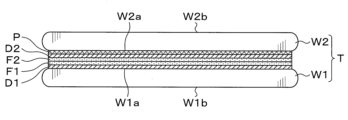
- FIG. 2 is a side view schematically showing the configuration of a polymerized wafer to be processed.
- FIG. 1 is a plan view schematically showing the configuration of a wafer processing system.
- FIG. 1 is a perspective view schematically showing the configuration of a wafer transfer device.
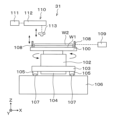
- FIG. 2 is a side view schematically showing the configuration of a laser irradiation device.
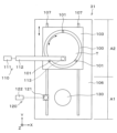
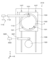
- FIG. 2 is a plan view schematically showing the configuration of a laser irradiation device.
- FIG. 3 is an explanatory diagram showing eccentricity of a first wafer and a second wafer.
- FIG. 3 is a side view showing how the separation device operates.
- FIG. 2 is an explanatory diagram showing how a laser absorption layer is irradiated with laser light.
- FIG. 1 is a plan view schematically showing the configuration of a wafer processing system.
- FIG. 1 is a perspective view schematically showing the configuration of a wafer transfer device.
- FIG. 2 is a side view schematically
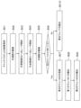
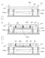
- FIG. 3 is a flow diagram showing the main steps of wafer processing. It is an explanatory view showing an example of irradiation of a laser beam to a laser absorption layer.
- FIG. 3 is an explanatory diagram of an unirradiated area generated in a laser absorption layer.
- FIG. 2 is an explanatory diagram showing an example of irradiating a non-irradiated area with a laser beam.
- FIG. 7 is an explanatory diagram showing another example of irradiating a non-irradiated region with a laser beam.
- FIG. 7 is an explanatory diagram showing another example of irradiating a non-irradiated region with a laser beam.
- FIG. 3 is an explanatory diagram showing the flow of a laser beam irradiation operation on a laser absorption layer.
- FIG. 3 is an explanatory diagram showing how a stacked wafer is transferred between a chuck and a transfer arm.
- FIG. 3 is an explanatory diagram showing how the stacked wafers are carried out from the separation device. It is a side view which shows another example of a structure of a laser irradiation device.
- FIG. 3 is an explanatory diagram showing an example of a region that is not irradiated with laser light and is set on a polymerized wafer.
- FIG. 7 is a plan view showing a configuration example of a laser irradiation device according to another embodiment.
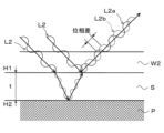
- FIG. 2 is an explanatory diagram that simply shows the operating principle of a spectroscopic interferometer.
- FIG. 7 is an explanatory diagram showing how an unbonded surface is inspected according to another embodiment.
- a device layer formed on the surface of the second wafer is transferred to the first wafer. is being carried out.
- This device layer transfer is performed using, for example, laser lift-off. That is, after reducing the bonding force between the first wafer and the second wafer by irradiating the inside of the polymerized wafer with laser light, the device layer is separated by separating the second wafer from the first wafer. Transfer to the first wafer.
- a laser irradiation device that irradiates a laser beam onto the polymerized wafer and a separation device that separates a first wafer and a second wafer are independently configured.
- the first wafer and the second wafer may be unintentionally separated.
- the second wafer may fall from the first wafer due to inertia caused by the transport operation of the stacked wafers. There is a risk of it getting lost.
- the technology according to the present disclosure has been made in view of the above circumstances, and when separating substrates based on the separation plane formed by irradiation with laser light, the technology according to the present disclosure is performed after irradiation with laser light and before separation of the substrates. To appropriately detect whether or not a substrate is separated. Note that in the following description, "separation" of the substrate to be detected refers to a state in which the second wafer is moving in the horizontal direction with respect to the first wafer.
- a state in which the bonding strength of the second wafer to the first wafer becomes zero and the second wafer can move independently with respect to the first wafer, and a state in which the bonding strength between the first wafer and the second wafer become zero Although the second wafer is still bonded, the bonding strength has decreased and the second wafer is horizontally displaced from the first wafer.
- a wafer processing system 1 In a wafer processing system 1 according to the present embodiment, which will be described later, as shown in FIG. 1, processing is performed on a stacked wafer T as a substrate in which a first wafer W1 and a second wafer W2 are bonded.
- the first wafer W1 the surface to be joined to the second wafer W2 will be referred to as the front surface W1a
- the surface opposite to the front surface W1a will be referred to as the back surface W1b.
- the surface to be bonded to the first wafer W1 is referred to as a front surface W2a
- the surface opposite to the front surface W2a is referred to as a back surface W2b.
- the first wafer W1 as the lower substrate is, for example, a semiconductor wafer such as a silicon substrate.
- the first wafer W1 has a substantially disk shape.
- a device layer D1 and a surface film F1 are laminated in this order from the front surface W1a side.
- Device layer D1 includes multiple devices.
- the surface film F1 include an oxide film (THOX film, SiO 2 film, TEOS film), SiC film, SiCN film, adhesive, and the like.
- the second wafer W2 as the upper substrate is also a semiconductor wafer such as a silicon substrate.
- the second wafer W2 has a substantially disk shape.
- a laser absorption layer P, a device layer D2, and a surface film F2 are laminated in this order from the front surface W2a side.
- the laser absorption layer P absorbs laser light irradiated from the laser irradiation section 110 as described later.
- an oxide film SiO 2 film
- the device layer D2 and the surface film F2 are similar to the device layer D1 and the surface film F1 of the first wafer W1, respectively.
- the wafer processing system 1 has a configuration in which a loading/unloading block 10, a transport block 20, and a processing block 30 are integrally connected.
- the loading/unloading block 10 and the processing block 30 are provided around the transport block 20.
- the carry-in/out block 10 is arranged on the Y-axis negative direction side of the conveyance block 20.
- a laser irradiation device 31 (described later) and a separation device 32 (described later) of the processing block 30 are located on the negative side of the X-axis of the transport block 20, and a first cleaning device 33 (described later) and a second cleaning device 34 (described later) are located on the X-axis negative side of the transport block 20.
- a reversing device 35 which will be described later, is arranged on the positive side of the X-axis and on the positive side of the Y-axis of the transport block 20, respectively.
- cassettes Ct, Cw1, and Cw2 each capable of accommodating a plurality of stacked wafers T, a plurality of first wafers W1, and a plurality of second wafers W2 are carried in and out of the carry-in/out block 10, respectively.
- the loading/unloading block 10 is provided with a cassette mounting table 11 .
- a plurality of cassettes for example, three cassettes Ct, Cw1, and Cw2, can be placed on the cassette mounting table 11 in a line in the X-axis direction. Note that the number of cassettes Ct, Cw1, and Cw2 placed on the cassette mounting table 11 is not limited to this embodiment, and can be arbitrarily determined.
- the three transport arms 23a to 23c are stacked in this order from above.
- the transport arms 23a to 23c are configured to be independently rotatable around vertical axes.
- a plurality of guide pins 25, for example three, are provided on the wafer holding surface of at least one of the three transfer arms 23a to 23c (the middle transfer arm 23b in the illustrated example).
- the guide pins 25 are arranged so as to surround the periphery of the stacked wafer T when the stacked wafer T is held by the transfer arm 23b.
- the guide pins 25 prevent the second wafer W2 from falling from above the first wafer W1 due to inertia or the like accompanying the transport of the stacked wafers T by the wafer transport device 22, as will be described later.
- the laser irradiation device 31 irradiates the inside of the polymerized wafer T, more specifically, the laser absorption layer P of the second wafer W2, with a laser beam to increase the bonding strength at the interface between the second wafer W2 and the laser absorption layer P. lower.
- the interface in this embodiment, the interface between the second wafer W2 and the laser absorption layer P
- the bonding strength is reduced inside the polymerized wafer T may be referred to as a "separation surface" in the technology of the present disclosure.
- a delivery position A1 and a processing position A2 are set inside the laser irradiation device 31.
- the transfer position A1 is a position where a wafer can be transferred between the transport arm 23 and a chuck 100, which will be described later, and a position where an image of the outer end of the stacked wafer T can be captured by an imaging mechanism 120, which will be described later.
- the processing position A2 is a position where the polymerized wafer T (laser absorption layer P) can be irradiated with laser light from a laser irradiation unit 110, which will be described later.
- the laser irradiation device 31 has a chuck 100 as a substrate holder that holds the superposed wafer T on its upper surface.
- the chuck 100 has a wafer holding surface on its upper surface, and holds the entire back surface W1b of the first wafer W1 by suction or a part of the radially inner side of the back surface W1b.
- the chuck 100 is, for example, an electrostatic chuck (ESC) or a vacuum chuck.
- the chuck 100 is provided with a lifting pin 100a (see FIG. 16) for supporting the stacked wafer T from below and lifting it up and down.
- the elevating pin 100a is inserted through a through hole (see FIG. 16) formed through the chuck 100, and is configured to be able to move up and down.
- the chuck 100 is provided with a plurality of, for example three, wafer fall prevention pins 101 as substrate fall prevention pins so as to surround the stacked wafer T on the holding surface along the radial direction.
- the wafer fall prevention pin 101 prevents the second wafer W2 from unintentionally separating from the first wafer W1 during or after laser beam irradiation due to, for example, centrifugal force accompanying the rotation of the chuck 100 or inertia force associated with movement. This prevents the second wafer W2 from falling from above the first wafer W1 when the second wafer W2 separates.
- the wafer fall prevention pin 101 is not particularly limited.
- the wafer fall prevention pin 101 is configured to be rotatable together with the chuck 100 by a rotation mechanism 104 described below, and movable in the Y-axis direction together with the chuck 100 by a drive mechanism 105 described later. Furthermore, it is configured to be able to move up and down in the Z-axis direction integrally with the above-mentioned lifting pin 100a.
- the chuck 100 is supported by a slider table 103 via an air bearing 102.
- a rotation mechanism 104 is provided on the lower surface side of the slider table 103.
- the rotation mechanism 104 has a built-in motor as a drive source, for example.
- the chuck 100 is configured to be rotatable around the ⁇ axis (vertical axis) by a rotation mechanism 104 via an air bearing 102 .
- the slider table 103 is movable between the above-mentioned delivery position A1 and processing position A2 by a drive mechanism 105 provided on the lower surface of the slider table 103 along a rail 107 provided on the base 106 and extending in the Y-axis direction. It is configured.
- the drive source of the drive mechanism 105 is not particularly limited, but a linear motor may be used, for example.
- the laser head 111 includes a laser oscillator (not shown) that oscillates laser light in a pulsed manner.
- This laser light is a so-called pulsed laser.
- the laser beam is a CO 2 laser beam, and the wavelength of the CO 2 laser beam is, for example, 8.9 ⁇ m to 11 ⁇ m.
- the laser head 111 may include equipment other than the laser oscillator, such as an amplifier.
- the lens 113 irradiates the polymerized wafer T held by the chuck 100 with laser light.
- the laser light emitted from the laser irradiation section 110 passes through the second wafer W2 and is irradiated onto the laser absorption layer P.
- the lens 113 may be configured to be movable up and down by a lifting mechanism (not shown).
- an imaging mechanism 120 as a detection mechanism is provided above the chuck 100 at the delivery position A1.
- the imaging mechanism 120 includes, for example, one or more cameras 121 selected from a macro camera, a micro camera, etc., and a calculation unit 122.
- the imaging mechanism 120 may be configured to be movable in the Y-axis direction and the Z-axis direction by a lifting mechanism (not shown) or a moving mechanism (not shown).
- a camera 121 serving as an acquisition unit images the outer end of the stacked wafer T held by the chuck 100.
- the camera 121 includes, for example, a coaxial lens, emits infrared light (IR), and receives reflected light from an object. Then, the camera 121 acquires position information of the stacked wafer T (at least the second wafer W2) on the chuck 100 by imaging the outer end of the stacked wafer T in this manner.
- the calculation unit 122 as a determination unit calculates the amount of eccentricity (horizontal direction (the amount of deviation with respect to the direction along the separation plane: see FIG. 6) is detected. Details of how the imaging mechanism 120 detects the eccentricity of the first wafer W1 and the second wafer W2 will be described later. In FIG.
- the acquisition unit (camera 121 or length measurement sensor) according to the technology of the present disclosure is arranged above the chuck 100 at the delivery position A1.
- the acquisition unit may be placed on the side of the chuck 100.
- a transport pad 130 is further provided above the chuck 100 at the delivery position A1.
- the transport pad 130 is configured to be able to be raised and lowered by a lifting mechanism (not shown). Further, the transport pad 130 has a suction surface on the lower surface side for suctioning and holding the first wafer W1. Then, the transport pad 130 detects that the first wafer W1 and the second wafer W2 are eccentric in the polymerized wafer T after the laser absorption layer P is irradiated with the laser beam by the imaging mechanism 120 described above. In this case, the second wafer W2 is transferred between the chuck 100 and the transfer arm 23. Note that details of the operation of the transport pad 130 will be described later.
- the separation device 32 separates the second wafer W2 from the first wafer W1 based on the interface between the second wafer W2 and the laser absorption layer P, which serves as a separation plane and whose bonding strength has been reduced by the laser irradiation device 31. .
- the separation device 32 includes a suction chuck 200 that suction-holds the back surface W1b of the first wafer W1 from below, and a suction pad 210 that suction-holds the back surface W2b of the second wafer W2 from above. and has.
- the suction chuck 200 is also provided with a lifting pin 200a for supporting the first wafer W1 from below and lifting it up and down.
- the lifting pin 200a is inserted through a through hole formed through the suction chuck 200, and is configured to be able to move up and down.
- the suction pad 210 is raised to separate the second wafer W2 from the laser absorption layer P, with the suction pad 210 suction-holding the second wafer W2, as shown in FIG.
- the first cleaning device 33 cleans the front surface W1a side of the first wafer W1 separated by the separation device 32. For example, a brush is brought into contact with the laser absorption layer P on the front surface W1a side of the first wafer W1 to clean the laser absorption layer P. Note that a pressurized cleaning liquid may be used to clean the first wafer W1. Further, the first cleaning device 33 may be configured to clean the front surface W1a side of the first wafer W1 as well as the back surface W1b.
- the above wafer processing system 1 is provided with a control device 40 as a control mechanism.
- the control device 40 is, for example, a computer, and has a program storage section (not shown).
- the program storage unit stores a program for controlling the processing of the stacked wafers T in the wafer processing system 1.
- the program storage unit also stores programs for controlling the operations of drive systems such as the various processing devices and transport devices described above to realize wafer processing in the wafer processing system 1, which will be described later.
- the above program may be one that has been recorded on a computer-readable storage medium H, and may have been installed in the control device 40 from the storage medium H. Further, the storage medium H may be temporary or non-temporary.
- a cassette Ct containing a plurality of stacked wafers T is placed on the cassette mounting table 11 of the loading/unloading block 10.
- the outer ends of the stacked wafers T (first wafer W1 and second wafer W2) on the chuck 100 that are suction-held by the chuck 100 are imaged using the imaging mechanism 120 (step St2 in FIG. 9). Specifically, while rotating the chuck 100, an image of the outer end of the stacked wafer T (the first wafer W1 and the first wafer W1) on the chuck 100 is captured by the camera 121. The position information of the second wafer W2) is acquired. The imaging result by the camera 121 is output to the calculation unit 122.
- the calculation unit 122 calculates the amount of eccentricity (horizontal deviation) between the rotation center of the chuck 100 and the center of the stacked wafer T (first wafer W1 and/or second wafer W2) based on the image taken by the camera 121. amount) may be calculated. If eccentricity is observed between the rotation center of the chuck 100 and the center of the stacked wafer T, it is desirable to perform eccentricity correction control in consideration of the eccentricity amount calculated when irradiating the laser beam L to the laser absorption layer P, which will be described later.
- the calculated eccentricity between the rotation center of the chuck 100 and the center of the superposed wafer T (second wafer W2) may be output to the control device 40.
- the chuck 100 is moved to the processing position A2 by the drive mechanism 105. Subsequently, irradiation of the laser light L (CO 2 laser light) from the laser irradiation unit 110 to the laser absorption layer P, more specifically, to the interface between the laser absorption layer P and the second wafer W2 is started.
- L CO 2 laser light
- the rotation mechanism 104 rotates the stacked wafer T held on the chuck 100, and the drive mechanism 105 moves the stacked wafer T in the Y-axis direction, while the laser beam is emitted.
- Light L is irradiated in a pulsed manner. Then, the irradiation position of the laser beam L is moved from the outside in the radial direction to the inside of the laser absorption layer P, and as a result, the laser beam L is irradiated spirally in a plan view as shown in FIG.
- the irradiation position of the laser beam L will be from the outside in the radial direction. As it moves inward, more specifically, as it approaches the rotation center of the chuck 100, the circumferential speed of the polymerized wafer T at the irradiation position of the laser beam L decreases, so it is necessary to increase the rotational speed of the polymerized wafer T. There is.
- the second wafer W2 is not displaced (separated) in the horizontal direction due to the centrifugal force associated with the rotation of the chuck 100 or the inertial force associated with the movement, and the second wafer W2 is not displaced (separated) in the horizontal direction by the centrifugal force associated with the rotation of the chuck 100 or the inertial force associated with the movement of the chuck 100. It refers to the bonding strength that can appropriately separate the second wafer W2 from the first wafer W1.
- the irradiation position of the laser light L is scanned in the X-axis direction, and the drive mechanism 105 moves the chuck 100 (polymerized wafer T) in the Y-axis direction. (See FIG. 10).
- a chuck is used for irradiating the central region R1 with the laser beam L.
- the laser light L is concentrically irradiated onto the laser absorption layer P so as to surround the central region R1. More specifically, when irradiating the outer peripheral region R2 with the laser beam L, the chuck 100 (polymerized wafer T) is rotated and moved in the Y-axis direction as described above, so that the laser beam L is spirally formed.
- the spirally processed portion in the outer peripheral region R2 is shown with a broken line and the concentrically processed portion is shown with a dashed line for clarity of illustration, but in reality, the spirally processed portion and the concentrically processed portion are shown with dashed lines.
- the irradiation interval of the laser beam L in the portion is constant.
- a plurality of regions having different conditions for irradiation with the laser beam L may be generated.
- the rotation of the chuck 100 is stopped/restarted every time the irradiation conditions of the laser beam L are changed, in other words, the chuck 100 is stopped when the irradiation conditions of the laser beam L are changed. If the laser processing is performed in a state where the laser processing is stopped, the time required for laser processing increases because acceleration/deceleration related to stopping/resuming the rotation takes time.
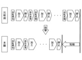
- the laser irradiation device 31 when changing the irradiation conditions of the laser beam L during irradiation of the laser beam L to the outer peripheral region R2, the irradiation of the laser beam L to the polymerized wafer T and the chuck It is desirable to stop only the movement of chuck 100 in the horizontal direction and continue rotation of chuck 100. By continuing to rotate the chuck 100 when the irradiation conditions of the laser beam L are changed in this way, as in the example of the present application shown in FIG. The time involved can be shortened.
- the irradiation restart position of the laser beam L after changing the irradiation conditions is the same as the irradiation end position of the laser beam L before changing the irradiation conditions. It may be the same position as , or it may be a different position as long as at least the irradiation positions of the laser beams L do not overlap.
- the irradiation restart position and the irradiation end position of the laser beam L are the same, after changing the irradiation conditions of the laser beam L, the laser beam L is rotated until the irradiation end position comes directly under the irradiation of the laser beam L.
- the interval at which the laser beam L is irradiated can be controlled to be constant over the entire surface of the laser absorption layer P, and the separation between the second wafer W2 and the laser absorption layer P can be controlled uniformly within the wafer surface.
- the irradiation restart position and the irradiation end position of the laser beam L are different, after changing the irradiation conditions of the laser beam L, immediately irradiate the laser beam L at least at a position where the irradiation positions of the laser beam L do not overlap. resume. In this case, the waiting time until the start of irradiation with the laser beam L can be reduced, and the time required for laser processing can be further shortened.
- the drive mechanism 105 When the central region R1 and the outer peripheral region R2 are irradiated with the laser beam L and the bonding strength is reduced over the entire surface of the second wafer W2 and the laser absorption layer P, the drive mechanism 105 then moves the chuck 100 (polymerized wafer T) is moved to the delivery position A1.
- the outer end of the stacked wafer T held by the chuck 100 is imaged using the imaging mechanism 120 (step St5 in FIG. 9). Specifically, while rotating the chuck 100, an image of the outer end of the stacked wafer T (the first wafer W1 and the first wafer W1) on the chuck 100 is captured by the camera 121. The position information of the second wafer W2) is acquired. The imaging result by the camera 121 is output to the calculation unit 122. The calculation unit 122 calculates the eccentricity of the first wafer W1 and the second wafer W2 after being irradiated with the laser beam L (see FIG. 6) based on the position information obtained from the imaging result by the camera 121. The calculated eccentricity of the first wafer W1 and the second wafer W2 after irradiation with the laser beam L may be output to the control device 40.
- the control device 40 determines the eccentricity of the first wafer W1 and the second wafer W2 before being irradiated with the output laser beam L, and the eccentricity of the first wafer W1 and the second wafer W2 after being irradiated with the laser beam L.
- the difference with the amount of eccentricity is calculated, and based on the difference value, it is determined whether the second wafer W2 is separated from the first wafer W1 (step St6 in FIG. 9).
- the superposed wafer T in which the bonding strength between the second wafer W2 and the laser absorption layer P has decreased is transferred to the first separation device 32 provided outside the laser irradiation device 31.
- the wafer W1 and the second wafer W2 are separated.
- the bonding strength between the second wafer W2 and the laser absorption layer P is reduced by irradiation with the laser beam L, the inertia force when moving the second wafer W2 to the delivery position A1 by the drive mechanism 105 and the chuck 100 Due to the centrifugal force accompanying the rotation, the second wafer W2 may be separated from the laser absorption layer P (first wafer W1) before being transferred to the separation device 32.
- the second wafer W2 is separated before being transferred to the separation device 32 in this way, there is a risk that not only will it not be possible to properly transfer the polymerized wafer T to the separation device 32, but also that the second wafer W2 may not be properly transferred to the separation device 32. There is a risk of the W2 falling and causing problems.
- step St6 it is determined whether or not the second wafer W2 has been separated from the first wafer W1 before transporting the polymerized wafer T to the separation device 32. It can be determined whether This prevents the wafer transfer device 22 from attempting to transfer the superposed wafer T in which the second wafer W2 is separated from the first wafer W1 to the separation device 32, and the second wafer W2 is This reduces the risk of dropping the item.
- a plurality of at least three wafer fall prevention pins 101 are provided so as to surround the overlapping wafer T held by the chuck 100.
- the superimposed wafer T for which it was determined that the second wafer W2 is separated from the first wafer W1 in step St6, is first held by the transfer pad 130 by suction and holding the back surface W2b of the second wafer W2.
- the transfer pad 130 is raised to remove the second wafer W2 from above the first wafer W1 (step St7 in FIG. 9).
- the first wafer W1 on the chuck 100 is transferred to the transfer arm 23c of the wafer transfer device 22, and the first wafer W1 is transferred from the laser irradiation device 31 (step St8 in FIG. 9).
- the first wafer W1 carried out from the laser irradiation device 31 is then transferred to the cassette Cw1 of the cassette mounting table 11 by the wafer transfer device 22. Further, the second wafer W2 carried out from the laser irradiation device 31 is turned upside down in the reversing device 35, that is, with the surface separated from the first wafer W1 facing upward. Thereafter, the wafer is transported by the wafer transport device 22 to the cassette Cw2 on the cassette mounting table 11. At this time, the first wafer W1 and the second wafer W2 are cleaned in the first cleaning device 33 and the second cleaning device 34, respectively, after their separation side surfaces W1a and W2a are cleaned, respectively.
- the cassettes may be transported to the cassettes Cw1 and Cw2 on the cassette mounting table 11, respectively.
- the superposed wafer T for which it is determined in step St6 that the second wafer W2 is not separated from the first wafer W1 is transferred from the chuck 100 to the transfer arm 23b of the wafer transfer device 22, and is transferred to the laser irradiation device. 31 (step St10 in FIG. 9).
- the wafer fall prevention pins 101 arranged so as to surround the periphery of the stacked wafer T held on the chuck 100 are integrated with the lifting pins 100a. It is configured to be able to move up and down in the Z-axis direction.
- the stacked wafer T is supported from below by the lifting pin 100a and raised, and then the holding surface of the chuck 100 and the lower surface of the stacked wafer T (the first This is carried out by inserting the transfer arm 23b between the back surfaces W1b) of the wafers W1, and then lowering the stacked wafers T using the lifting pins 100a.
- the wafer drop prevention pins 101 can surround the stacked wafers T even when the lift pins 100a are rising. This makes it possible to suppress the second wafer W2 from falling during transfer from the chuck 100 to the transfer arm 23b.
- the periphery of the polymerized wafer T is A transport arm 23b having guide pins 25 arranged in a surrounding manner is used. As a result, even if the second wafer W2 is separated from the first wafer W1, the second wafer W2 is can be prevented from falling.
- the polymerized wafer T carried out from the laser irradiation device 31 is then transferred to the separation device 32 by the wafer transfer device 22.
- a suction chuck 200 suction-holds the back surface W1b of the first wafer W1
- a suction pad 210 suction-holds the back surface W2b of the second wafer W2.
- the suction pad 210 is raised to separate the first wafer W1 and the second wafer W2.
- the bonding strength at the interface between the laser absorption layer P and the second wafer W2 is reduced by the irradiation with the laser beam L, so the second wafer W2 can be separated without applying a large load. .
- the separated second wafer W2 is transferred from the suction pad 210 to the transfer arm 23a of the wafer transfer device 22, and then transferred to the reversing device 35, as shown in FIG. Then, after the surface W2a is turned upward in the reversing device 35, it is transported to the second cleaning device 34.
- the front surface W2a which is the side separated from the first wafer W1 is cleaned.
- the second cleaning device 34 may clean both the front surface W2a and the back surface W2b. Further, separate cleaning sections may be provided to clean the front surface W2a and the back surface W2b, respectively. Thereafter, the second wafer W2 that has been cleaned by the second cleaning device 34 is transferred to the cassette Cw2 of the cassette mounting table 11 by the wafer transfer device 22.
- the first wafer W1 held by the suction chuck 200 is transferred to the transfer arm 23c and transferred to the first cleaning device 33, as shown in FIG.
- This transfer by the transfer arm 23c may be performed simultaneously with the transfer of the second wafer W2 by the transfer arm 23a, or may be performed independently.
- the surface W1a side that is the side separated from the second wafer W2, specifically, the surface of the laser absorption layer P is cleaned.
- the back surface W1b of the first wafer W1 may be cleaned together with the front surface of the laser absorption layer P.
- separate cleaning sections may be provided to clean the front surface of the laser absorption layer P and the back surface W1b of the first wafer W1, respectively.
- the first wafer W1 that has been cleaned by the first cleaning device 33 is transferred to the cassette Cw1 of the cassette mounting table 11 by the wafer transfer device 22.
- the amount of eccentricity of the second wafer W2 with respect to the first wafer W1 before and after irradiation of the laser beam L to the polymerized wafer T (laser absorption layer P) Separation of the second wafer W2 was detected based on the difference value.
- the configuration of the second wafer W2 detection mechanism and the detection method using the same are not limited, and may include at least one of the following configurations and methods instead of or in addition to the above configurations and methods. Good too.
- the acceleration required to move the chuck 100 from the processing position A2 to the delivery position A1 after irradiation with the laser beam L is compared to the acceleration of the chuck 100 from the delivery position A1 to the processing position A2 before the irradiation with the laser beam
- the acceleration may be made larger than the acceleration required for movement of the superposed wafer T to apply an inertial force as a load.
- the magnitude of the load applied to the polymerized wafer T after irradiation with the laser beam L is such that the separated second wafer W2 can be shifted on the first wafer W1, and the second wafer W2 is If not separated, the size is controlled to such an extent that the second wafer W2 does not shift on the first wafer W1 (the second wafer W2 is not separated).
- the first wafer W1 and the second wafer W2 are intentionally eccentric (horizontal misalignment). bring about This makes it possible to avoid the situation where eccentricity does not occur even though the second wafer W2 is separated from the first wafer W1, as described above, and as a result, the second wafer The fear that W2 will fall from the first wafer W1 can be further appropriately suppressed.
- both the imaging mechanism 120 as a detection mechanism and the contact sensor 108 may be arranged in the laser irradiation device 31. In this case, both the detection of separation of the first wafer W1 and the second wafer W2 by the imaging mechanism 120 and the detection by the contact sensor 108 may be performed. In this case, when contact between the contact sensor 108 and the second wafer W2 is detected, the imaging mechanism 120 detects the separation of the first wafer W1 and the second wafer W2 (the outer edge of the superimposed wafer T imaging) may be omitted.
- the first wafers before and after irradiation with the laser beam L are obtained by imaging the outer ends of the stacked wafers T (the first wafer W1 and the second wafer W2) by the imaging mechanism 120. Separation of the second wafer W2 was detected based on the difference in eccentricity between the wafer W1 and the second wafer W2.
- the imaging mechanism 120 does not necessarily need to perform imaging of the outer ends of the stacked wafers T (the first wafer W1 and the second wafer W2) before and after the irradiation of the laser beam L, but only after the irradiation of the laser beam L. may be carried out.
- the first images before and after irradiation with the laser beam L are obtained by imaging the outer ends of the stacked wafers T (the first wafer W1 and the second wafer W2) using the imaging mechanism 120. Separation of the second wafer W2 was detected based on the difference in eccentricity between the wafer W1 and the second wafer W2.
- the imaging mechanism 120 may not be able to image the outer end of the first wafer W1 as the lower substrate on the chuck 100.
- the imaging mechanism 120 may image only the outer end of the second wafer W2 as the upper substrate.
- the position information of the second wafer W2 on the chuck 100 before and after the irradiation with the laser beam L is acquired from the imaging result by the imaging mechanism 120, and the position information of the second wafer W2 relative to the center of the chuck 100 before and after the irradiation with the laser beam L is acquired.
- the horizontal eccentricity (shift amount) of the center (more specifically, the rotation center) of the wafer W2 is detected.
- the difference between the amount of eccentricity of the center of the second wafer W2 with respect to the center of the chuck 100 before irradiation with the laser beam and the amount of eccentricity of the center of the second wafer W2 with respect to the center of the chuck 100 after irradiation with the laser beam is calculated.
- the imaging mechanism 120 images the outer ends of the stacked wafers T (the first wafer W1 and the second wafer W2) at 360 degrees in the circumferential direction.
- the eccentricity of the second wafer W2 was calculated, and separation of the second wafer W2 was detected.
- the imaging mechanism 120 does not necessarily need to image the outer ends of the stacked wafers T (the first wafer W1 and the second wafer W2) at 360 degrees in the circumferential direction; Separation of the second wafer W2 can also be detected by capturing images at two locations (for example, a point at the reference position in the circumferential direction of 0 degrees and a point at 90 degrees in the circumferential direction from the reference position).
- the second Separation of wafer W2 can be detected. Therefore, the time required for imaging the outer end portion by the imaging mechanism 120 after irradiation with the laser beam L can be shortened, and thereby the takt time required for processing in the laser irradiation device 31 can be reduced.
- the laser irradiation unit 110 irradiates the central region R1 and the outer peripheral region R2 with the laser beam L to reduce the bonding strength over the entire surface of the second wafer W2 and the laser absorption layer P.
- the bonding strength is reduced across the entire surface of the second wafer W2 and the laser absorption layer P, as described above, there is a risk that the second wafer W2 will fall due to the inertial force when the polymerized wafer T is transported. be.
- the irradiation of the laser beam L is stopped in at least a part of the interface between the second wafer W2 and the laser absorption layer P, and the irradiation of the laser beam L is stopped in at least a part of the interface between the second wafer W2 and the laser absorption layer P.
- the bonding strength between the second wafer W2 and the laser absorption layer P may be maintained in this region. More specifically, in the wafer processing system 1, as shown in FIG. 19, at the interface between the second wafer W2 and the laser absorption layer P, the outermost peripheral region R0 (in FIG. The bonding strength between the second wafer W2 and the laser absorption layer P is increased in the central region R3 (see FIG. 19(b)), which is set near the center position of the central region R1. It is also possible to form a region that does not reduce the
- the "acquisition unit" of the detection mechanism is a length measurement sensor (displacement sensor) instead of the camera 121 as described above. total) can be used.
- the transport arm 23b equipped with the guide pin 25 is used to transport the first wafer W1 and the second wafer W2, as in step St10.
- the first wafer W1 and the second wafer W2 may be unloaded from the laser irradiation device 31.
- the lifting speed of the stacked wafer T by the lifting pin 100a and the transport speed of the stacked wafer T by the wafer transport device 22 are set as normal. It is desirable to control the moving speed to be lower than the specified moving speed (when separation of the second wafer W2 is not detected in step St6).
- the wafer processing method of the present disclosure was applied when performing laser lift-off to separate the second wafer W2 from the laser absorption layer P.
- the technique according to the present disclosure in the polymerized wafer T in which the first wafer W1 and the second wafer W2 are bonded, at least a portion of the first wafer W1 and/or the second wafer W2 is transferred to the polymerized wafer T. It can be applied arbitrarily as long as it is separated from the
- a spectral interferometer is arranged in the laser irradiation device 31, and the interface between the first wafer W1 and the second wafer W2 (more specifically, the second wafer
- the second wafer W2 is separated from the first wafer W1. It may also be determined whether or not they are separated.
- a spectral interferometer 320 is arranged in a laser irradiation device 310 according to another embodiment.
- Spectroscopic interferometer 320 includes a head 321 and an analysis section 322.
- the head 321 includes an irradiation unit (not shown) that irradiates the overlapping wafer T on the chuck 100 with measurement light, and a irradiation unit (not shown) that irradiates the overlapping wafer T on the chuck 100 at different height positions (a first height position H1 and a second height position H2: FIG. and a spectroscopy unit (not shown) that receives the measurement light (reflected light) reflected by the laser beam (refer to FIG. 22) and detects interference between the reflected lights.
- a spectroscopy unit not shown
- As the measurement light irradiated from the irradiation section light that is transparent to the second wafer W (silicon) is arbitrarily selected.
- the central region R1 and the outer peripheral region R2 are irradiated with the laser beam L, and the bonding strength of the second wafer W2 and the laser absorption layer P is reduced over the entire surface of the stacked wafer T. 105 below the spectroscopic interferometer 320.
- the measurement light L2 from the irradiation part of the head 321 is irradiated toward the polymerized wafer T, and the reflected light from the polymerized wafer T enters the spectroscopic unit.
- the spectroscopy unit when interference of reflected light (reflection spectrum) is detected on the entire surface of the superposed wafer T, it is determined that the second wafer W2 is separated from the first wafer W1.
- the spectroscopic interferometer 320 may be moved and rotated relatively above the chuck 100 (polymerized wafer T). Furthermore, for example, by configuring the spectral interferometer 320 side by side with the laser irradiation device 310 or integrally with the laser irradiation device 310, the bonding strength reduction process by the laser irradiation device 310 and the separation determination by the spectral interferometer 320 can be performed simultaneously or sequentially. You may also do so.
- a more specific method of determining separation between the second wafer W2 and the first wafer W1 using the spectroscopic interferometer 320 will be described.
- the bonding strength at the interface between the second wafer W2 and the laser absorption layer P decreases due to irradiation with the laser beam L, and the second wafer W2 is separated from the first wafer W1, as shown in FIGS. 21 and 22.
- a space S which is a gap between the two, is formed.
- the analysis unit 322 calculates the thickness t of the space S (the first height position H1 and the second height position H2) based on this. Calculate the distance between The calculated thickness t of the space S is output to the control device 40.
- the control device 40 can determine whether the space S is formed at the interface between the second wafer W2 and the laser absorption layer P based on the output thickness t. When it is determined that the space S is formed over the entire surface of the polymerized wafer T (laser absorption layer P), the second wafer W2 and the laser absorption layer P have completely separated, and this means that the second wafer W2 and the laser absorption layer P have completely separated. It can be determined that wafer W2 is separated from first wafer W1.
- the calculated thickness t of the space S can be used as the value used as the first threshold value.
- the first threshold value is a value at which it is determined that the space S has been formed, and is a value greater than t>0, which is the thickness at which it is determined that the space S has been formed.
- the first threshold used for comparison may be set to a value greater than zero.
- the detection of reflected light from the polymerized wafer T using the spectroscopic interferometer 320 is performed using the polymerized wafer T (laser absorption layer P) in order to appropriately detect separation of the second wafer W2 from the first wafer W1. It is desirable that this be carried out across the board. However, for the purpose of shortening the time required for inspection and improving throughput, only a portion of the irradiation pitch of the laser beam L irradiated to the laser absorption layer P (for example, a portion of the radial direction or circumferential direction) is used. only).
- the spectroscopic interferometer 320 for detecting the separation of the first wafer W1 and the second wafer W2 is arranged inside the laser irradiation device 310 has been described as an example.
- the spectral interferometer 320 may be placed outside the laser irradiation device 310. That is, in the technology according to the present disclosure, the wafer processing system 1 includes a laser irradiation device 31 and an inspection device ( (not shown) may be arranged independently.
- the method of inspecting the separation state is not limited to this.
- this region may be at the same height as the optical flat. For example, it is determined that the space S is not formed.
- the space S which is the measurement result used for comparison with the first threshold in the above embodiment, is Instead of the thickness t, the amount of change t2 (see FIG. 22) in the height of the stacked wafer T that changes due to the formation of the space S can be used as the measurement result used for comparison with the first threshold value.
- a displacement meter (not shown) may be provided above the chuck 100, and the distance from the displacement meter to the back surface W2b of the second wafer W2 may be measured. good.
- the amount of change in the distance to the back surface W2b of the second wafer W2 before and after the formation of the space S, or the area where the distance to the back surface W2b and the bonding strength in the region where the space S is formed is not reduced.
- Separation of the first wafer W1 and the second wafer W2 may be determined by detecting the difference between the distance to the back surface W2b and the like (see FIG. 19).
- the device in the configuration of the laser irradiation device 310 shown in FIG. 20, the device can be configured only by changing the spectral interferometer 320 to a displacement meter (length measurement sensor) not shown.
- the laser beam L was sequentially irradiated to the preset central region R1 and outer peripheral region R2 (see FIG. 10) of the chuck 100.
- the determination as to whether or not to irradiate the central region R1 with the laser beam L may be made, for example, prior to irradiating the central region R1 with the laser beam L.
- the irradiation of the laser beam L to the central region R1 is continued. conduct.
- the overlapping wafer T in which the bonding strength between the second wafer W2 and the laser absorption layer P has decreased is then transferred to the separating device 32, where the first wafer W1 and the second wafer W2 are separated.
- the central region R1 is not irradiated with the laser beam L. Therefore, the bonding strength between the second wafer W2 and the laser absorption layer P is maintained in the central region R1.
- the polymerized wafer T is recovered from the laser irradiation device without being transported to the separation device 32. At this time, the polymerized wafer T may be collected into a cassette via a transport device, or may be removed from the laser irradiation device by manual collection by an operator.
- the second wafer W2 including the central region R1 and the laser absorption layer It is possible to suppress complete peeling of the entire surface of the interface between P and safely transport the polymerized wafer T without dropping the second wafer W2 within the laser irradiation device.
- the positional information of the peripheral region R2 is acquired prior to irradiating the peripheral region R2 with the laser beam L, and the positional information before the laser beam L is irradiated and the positional information after the laser beam L is irradiated are obtained.
- the state of peeling was determined by comparison with However, if the peeling state in the outer peripheral region R2 can be determined without comparing the positional information before and after irradiation with the laser beam L, it is not necessarily necessary to acquire the positional information before the irradiation with the laser beam L, and at least the laser beam to the central region R1 Before irradiating the light L, position information and the like may be acquired to check the peeling state.
- the laser absorption layer P, the device layer D2, and the surface film F2 are laminated in this order on the front surface W2a of the second wafer W2, and the interface between the laser absorption layer P and the second wafer W2 is
- the separation plane is set as the separation plane between the first wafer W1 and the second wafer W2
- the position of the separation plane is not limited thereto.
- a peeling process is performed between the second wafer W2 and the laser absorption layer P to promote peeling of the first wafer W1 and the second wafer W2.
- a promoting film (not shown) may be formed and the interface between the peel promoting film and the second wafer W2 may be set as a separation plane.
- the material constituting the peel-promoting film is such that the adhesion between the peel-promoting film and the second wafer W2 (silicon, etc.) It is desirable to select one that is at least smaller than the adhesion force between them.
Landscapes
- Physics & Mathematics (AREA)
- Engineering & Computer Science (AREA)
- Optics & Photonics (AREA)
- Chemical & Material Sciences (AREA)
- General Physics & Mathematics (AREA)
- Biochemistry (AREA)
- Health & Medical Sciences (AREA)
- Analytical Chemistry (AREA)
- Immunology (AREA)
- Pathology (AREA)
- Life Sciences & Earth Sciences (AREA)
- General Health & Medical Sciences (AREA)
- Plasma & Fusion (AREA)
- Mechanical Engineering (AREA)
- Oil, Petroleum & Natural Gas (AREA)
- General Chemical & Material Sciences (AREA)
- Chemical Kinetics & Catalysis (AREA)
- Container, Conveyance, Adherence, Positioning, Of Wafer (AREA)
- Robotics (AREA)
- Laser Beam Processing (AREA)
Priority Applications (5)
| Application Number | Priority Date | Filing Date | Title |
|---|---|---|---|
| JP2024526287A JP7806234B2 (ja) | 2022-06-07 | 2023-04-25 | 基板処理システム及び基板処理方法 |
| KR1020257000117A KR20250021367A (ko) | 2022-06-07 | 2023-04-25 | 기판 처리 시스템 및 기판 처리 방법 |
| CN202380042527.8A CN119256388A (zh) | 2022-06-07 | 2023-04-25 | 基板处理系统和基板处理方法 |
| US18/872,334 US20250316507A1 (en) | 2022-06-07 | 2023-04-25 | Substrate processing system and substrate processing method |
| JP2026004539A JP2026063154A (ja) | 2022-06-07 | 2026-01-14 | 基板処理システム及び基板処理方法 |
Applications Claiming Priority (4)
| Application Number | Priority Date | Filing Date | Title |
|---|---|---|---|
| JP2022092479 | 2022-06-07 | ||
| JP2022-092479 | 2022-06-07 | ||
| JP2022202376 | 2022-12-19 | ||
| JP2022-202376 | 2022-12-19 |
Publications (1)
| Publication Number | Publication Date |
|---|---|
| WO2023238542A1 true WO2023238542A1 (ja) | 2023-12-14 |
Family
ID=89118085
Family Applications (1)
| Application Number | Title | Priority Date | Filing Date |
|---|---|---|---|
| PCT/JP2023/016360 Ceased WO2023238542A1 (ja) | 2022-06-07 | 2023-04-25 | 基板処理システム及び基板処理方法 |
Country Status (6)
| Country | Link |
|---|---|
| US (1) | US20250316507A1 (https=) |
| JP (2) | JP7806234B2 (https=) |
| KR (1) | KR20250021367A (https=) |
| CN (1) | CN119256388A (https=) |
| TW (1) | TW202401554A (https=) |
| WO (1) | WO2023238542A1 (https=) |
Cited By (1)
| Publication number | Priority date | Publication date | Assignee | Title |
|---|---|---|---|---|
| WO2025009324A1 (ja) * | 2023-07-05 | 2025-01-09 | 東京エレクトロン株式会社 | 処理システム及び処理方法 |
Citations (5)
| Publication number | Priority date | Publication date | Assignee | Title |
|---|---|---|---|---|
| WO2020213479A1 (ja) * | 2019-04-19 | 2020-10-22 | 東京エレクトロン株式会社 | 処理装置及び処理方法 |
| WO2021006091A1 (ja) * | 2019-07-10 | 2021-01-14 | 東京エレクトロン株式会社 | 分離装置及び分離方法 |
| JP2021019056A (ja) * | 2019-07-18 | 2021-02-15 | 東京エレクトロン株式会社 | 処理装置及び処理方法 |
| WO2021131711A1 (ja) * | 2019-12-26 | 2021-07-01 | 東京エレクトロン株式会社 | 基板処理方法及び基板処理装置 |
| JP2021106197A (ja) * | 2019-12-26 | 2021-07-26 | 東京エレクトロン株式会社 | 基板処理装置及び基板処理方法 |
Family Cites Families (1)
| Publication number | Priority date | Publication date | Assignee | Title |
|---|---|---|---|---|
| JP2007220749A (ja) | 2006-02-14 | 2007-08-30 | Seiko Epson Corp | 半導体装置の製造方法 |
-
2023
- 2023-04-25 CN CN202380042527.8A patent/CN119256388A/zh active Pending
- 2023-04-25 KR KR1020257000117A patent/KR20250021367A/ko active Pending
- 2023-04-25 US US18/872,334 patent/US20250316507A1/en active Pending
- 2023-04-25 WO PCT/JP2023/016360 patent/WO2023238542A1/ja not_active Ceased
- 2023-04-25 JP JP2024526287A patent/JP7806234B2/ja active Active
- 2023-05-09 TW TW112117062A patent/TW202401554A/zh unknown
-
2026
- 2026-01-14 JP JP2026004539A patent/JP2026063154A/ja active Pending
Patent Citations (5)
| Publication number | Priority date | Publication date | Assignee | Title |
|---|---|---|---|---|
| WO2020213479A1 (ja) * | 2019-04-19 | 2020-10-22 | 東京エレクトロン株式会社 | 処理装置及び処理方法 |
| WO2021006091A1 (ja) * | 2019-07-10 | 2021-01-14 | 東京エレクトロン株式会社 | 分離装置及び分離方法 |
| JP2021019056A (ja) * | 2019-07-18 | 2021-02-15 | 東京エレクトロン株式会社 | 処理装置及び処理方法 |
| WO2021131711A1 (ja) * | 2019-12-26 | 2021-07-01 | 東京エレクトロン株式会社 | 基板処理方法及び基板処理装置 |
| JP2021106197A (ja) * | 2019-12-26 | 2021-07-26 | 東京エレクトロン株式会社 | 基板処理装置及び基板処理方法 |
Cited By (1)
| Publication number | Priority date | Publication date | Assignee | Title |
|---|---|---|---|---|
| WO2025009324A1 (ja) * | 2023-07-05 | 2025-01-09 | 東京エレクトロン株式会社 | 処理システム及び処理方法 |
Also Published As
| Publication number | Publication date |
|---|---|
| US20250316507A1 (en) | 2025-10-09 |
| KR20250021367A (ko) | 2025-02-12 |
| JPWO2023238542A1 (https=) | 2023-12-14 |
| CN119256388A (zh) | 2025-01-03 |
| JP7806234B2 (ja) | 2026-01-26 |
| TW202401554A (zh) | 2024-01-01 |
| JP2026063154A (ja) | 2026-04-10 |
Similar Documents
| Publication | Publication Date | Title |
|---|---|---|
| JP7413468B2 (ja) | 基板処理装置及び基板処理方法 | |
| JP6145415B2 (ja) | 剥離方法、プログラム、コンピュータ記憶媒体、剥離装置及び剥離システム | |
| JP7178491B2 (ja) | 処理装置及び処理方法 | |
| JP7780534B2 (ja) | 処理方法及び処理システム | |
| JP7611350B2 (ja) | 基板処理装置及び基板処理方法 | |
| JP7851390B2 (ja) | 処理方法及び処理システム | |
| KR20190119803A (ko) | 웨이퍼의 에지 영역 검사장치 및 검사방법 | |
| KR102323122B1 (ko) | 접합 시스템 및 접합 방법 | |
| JP2026063154A (ja) | 基板処理システム及び基板処理方法 | |
| JP7129549B2 (ja) | 処理装置及び処理方法 | |
| WO2023176519A1 (ja) | 基板処理装置及び基板処理方法 | |
| JP2017139492A (ja) | 基板処理方法および基板処理装置 | |
| JP6120791B2 (ja) | 剥離方法、プログラム、コンピュータ記憶媒体、剥離装置及び剥離システム | |
| JP2021012950A (ja) | 支持体剥離方法及び支持体剥離システム | |
| JP7843650B2 (ja) | 基板処理装置及び位置調整方法 | |
| WO2025009324A1 (ja) | 処理システム及び処理方法 | |
| KR20250110463A (ko) | 비접촉 웨이퍼 에지 검사 장치 | |
| WO2026004649A1 (ja) | 基板処理システム、基板処理方法、プログラム及び記憶媒体 | |
| WO2026004650A1 (ja) | 基板処理システム、基板処理方法、プログラム及び記憶媒体 |
Legal Events
| Date | Code | Title | Description |
|---|---|---|---|
| 121 | Ep: the epo has been informed by wipo that ep was designated in this application |
Ref document number: 23819529 Country of ref document: EP Kind code of ref document: A1 |
|
| WWE | Wipo information: entry into national phase |
Ref document number: 202380042527.8 Country of ref document: CN |
|
| WWE | Wipo information: entry into national phase |
Ref document number: 2024526287 Country of ref document: JP |
|
| WWE | Wipo information: entry into national phase |
Ref document number: 18872334 Country of ref document: US |
|
| ENP | Entry into the national phase |
Ref document number: 20257000117 Country of ref document: KR Kind code of ref document: A |
|
| WWE | Wipo information: entry into national phase |
Ref document number: 1020257000117 Country of ref document: KR |
|
| WWP | Wipo information: published in national office |
Ref document number: 202380042527.8 Country of ref document: CN |
|
| NENP | Non-entry into the national phase |
Ref country code: DE |
|
| WWP | Wipo information: published in national office |
Ref document number: 1020257000117 Country of ref document: KR |
|
| 122 | Ep: pct application non-entry in european phase |
Ref document number: 23819529 Country of ref document: EP Kind code of ref document: A1 |
|
| WWP | Wipo information: published in national office |
Ref document number: 18872334 Country of ref document: US |