WO2023238391A1 - 太陽電池およびその製造方法 - Google Patents
太陽電池およびその製造方法 Download PDFInfo
- Publication number
- WO2023238391A1 WO2023238391A1 PCT/JP2022/023471 JP2022023471W WO2023238391A1 WO 2023238391 A1 WO2023238391 A1 WO 2023238391A1 JP 2022023471 W JP2022023471 W JP 2022023471W WO 2023238391 A1 WO2023238391 A1 WO 2023238391A1
- Authority
- WO
- WIPO (PCT)
- Prior art keywords
- solar cell
- layer
- cell according
- base material
- electrode
- Prior art date
- Legal status (The legal status is an assumption and is not a legal conclusion. Google has not performed a legal analysis and makes no representation as to the accuracy of the status listed.)
- Ceased
Links
Images




Classifications
-
- H—ELECTRICITY
- H10—SEMICONDUCTOR DEVICES; ELECTRIC SOLID-STATE DEVICES NOT OTHERWISE PROVIDED FOR
- H10F—INORGANIC SEMICONDUCTOR DEVICES SENSITIVE TO INFRARED RADIATION, LIGHT, ELECTROMAGNETIC RADIATION OF SHORTER WAVELENGTH OR CORPUSCULAR RADIATION
- H10F77/00—Constructional details of devices covered by this subclass
- H10F77/30—Coatings
Definitions
- Embodiments of the present invention relate to a solar cell and a method for manufacturing the same.
- thin-film solar cells have been attracting attention in recent years.
- thin-film solar cells we used thin-film silicon solar cells using Si thin films, CIGS solar cells using copper-indium-gallium-selenium (CIGS)-based thin films, and copper-indium-sulfur (CIS)-based thin films.
- CIGS solar cells using copper-indium-gallium-selenium (CIGS)-based thin films
- CIS solar cells and the like are being researched, and all of these solar cells are attracting attention as solar cells that can be expected to have high conversion efficiency.
- the above-mentioned thin film solar cells are also called flexible thin film solar cells because they can be formed on resin films or metal thin films.
- Flexible thin-film solar cells are lightweight and have excellent flexibility, so there are fewer restrictions on where they can be installed than conventional solar cells; for example, they can be installed freely on the roof of large equipment or on curved surfaces. I can do it.
- thin-film solar cells with a protective cover containing a photocatalyst on the light-receiving surface are also being considered.
- the conventional thin film solar cells described above are extremely lightweight, they have insufficient weather resistance and fire resistance, and are desired to have durability that can withstand long-term use. Further, when a photocatalyst layer is provided on the surface of a thin film solar cell to prevent pollution, there is a problem in that other layers (particularly organic films, etc.) adjacent to the photocatalyst layer are deteriorated by the photocatalyst. Furthermore, when layers according to required characteristics are laminated on a thin film solar cell, there is also a problem that each layer tends to peel off.
- the problem to be solved by the present invention is to provide a solar cell that has excellent weather resistance and fire resistance, whose surface is resistant to dirt and peeling, and a method for manufacturing the same.
- the solar cell of the embodiment includes a flexible solar cell sheet and a laminate provided on the light-receiving surface of the flexible solar cell sheet.
- the laminate includes a base material, a base layer, and a photocatalyst layer in this order.
- the base material is disposed on the light-receiving surface of the flexible solar cell sheet and has a negative zeta potential in pH 7 water.
- the underlayer is disposed on the substrate and has a positive zeta potential in pH 7 water.
- the photocatalytic layer is disposed on the base layer, contains a photocatalytic material, and has a negative or zero zeta potential in pH 7 water.
- FIG. 1 is a cross-sectional view showing the solar cell of the first embodiment.
- FIG. 2 is a cross-sectional view showing a solar cell according to a second embodiment.
- FIG. 3 is a cross-sectional view showing the laminate of Example 1.
- FIG. 3 is a cross-sectional view showing a laminate of Example 2.
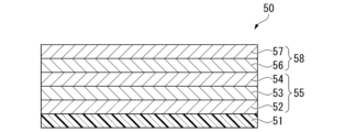
- FIG. 3 is a cross-sectional view showing a laminate of Example 3.
- FIG. 4 is a cross-sectional view showing a solar cell of Example 4.
- FIG. 3 is a cross-sectional view showing a solar cell of Example 5.
- FIG. 6 is a cross-sectional view showing a solar cell of Example 6.
- the first embodiment relates to a flexible thin film solar cell having optical transparency.
- the configuration of the flexible thin-film solar cell (hereinafter sometimes simply referred to as a solar cell) of this embodiment will be described below.
- FIG. 1 shows a conceptual cross-sectional diagram of a solar cell 1 according to a first embodiment.
- the solar cell 1 according to the present embodiment includes a flexible solar cell sheet 10 and a laminate 20 provided on the light-receiving surface of the flexible solar cell sheet 10.
- the laminate 20 includes a base material 21, a base layer 22, and a photocatalyst layer 23 in this order.
- the "light-receiving surface” as used in this specification means the surface of the flexible solar cell sheet 10 on the side where sunlight is incident.
- the upper surface of flexible solar cell sheet 10 is the "light-receiving surface.”
- the details of the laminate 20 will be explained below. Note that the flexible solar cell sheet 10 will be detailed later.
- a laminate 20 including a base material 21, a base layer 22, and a photocatalyst layer 23 is provided on the light-receiving surface of the flexible solar cell sheet 10 in order to improve weather resistance, fire resistance, and prevent pollution.
- Base material 21 is placed on the light-receiving surface of flexible solar cell sheet 10 .
- the base material 21 may contain a resin containing a halogen element, or may be composed only of a resin containing a halogen element.
- the resin constituting the base material 21 is preferably a flame-retardant resin. It is more preferable to use a resin having flame retardancy of grade "V-0" or higher according to the UL94 standard, such as polyvinyl chloride (PVC), polyvinylidene chloride (PVDC), polyvinylidene fluoride (PVDF), and polycarbonate (PC). ).
- PVC polyvinyl chloride
- PVDC polyvinylidene chloride
- PVDF polyvinylidene fluoride
- PC polycarbonate
- the base material 21 has a negative zeta potential in water with a pH of 7.
- the bonding strength (peeling resistance) with the base layer 22 having a positive zeta potential can be increased, and the bonding strength between the base material 21 and the base layer 22 can be increased. Peeling can be prevented.
- the reason for specifying "underwater with a pH of 7" here is that it is assumed that the device will be used in the normal atmosphere, and for example, it is assumed that the device will be wet with dew or rainwater.
- the zeta potential fluctuates somewhat when the pH changes, but it does not change rapidly.
- the pH of the base material 21 is preferably negative within the range of 4 to 7. It is known that polymers containing a halogen element or a carbonyl group tend to have a negative zeta potential because the negative polarity is on the outside.
- the thickness of the base material 21 is not particularly limited, but from the viewpoint of handling, it may be in the range of 10 to 100 ⁇ m. Preferably it is 30 to 80 ⁇ m.
- Base layer 22 is placed on base material 21 .
- Underlayer 22 has a positive zeta potential in water with a pH of 7. Thereby, the bonding strength with the base material 21 and the photocatalyst layer 23, each of which has a negative zeta potential, can be increased. If there is no base layer 22, the photocatalytic layer 23, which has a negative or zero (neutral) zeta potential, and the base material 21, which has a negative zeta potential, repel each other, so that the photocatalytic layer 23 is likely to peel off.
- a base layer 22 having a different zeta potential is provided between the base material 21 and the photocatalyst layer 23. It is effective to provide Further, by providing the base layer 22 between the photocatalytic layer 23 and the base material 21, direct contact between the photocatalytic layer 23 and the base material 21 can be avoided, thereby preventing deterioration of the base material 21 due to photocatalytic action. can.
- the underlying layer 22 preferably has a positive pH within the range of 4 to 7.
- the base layer 22 contains an inorganic compound.
- the inorganic compound include inorganic oxides such as aluminum oxide and zirconium oxide, and inorganic nitrides such as silicon nitride.
- inorganic oxides such as aluminum oxide and zirconium oxide
- inorganic nitrides such as silicon nitride.
- aluminum oxide and silicon nitride are preferred.
- Aluminum oxide and silicon nitride have positive zeta potential over a wide pH range and have the effect of preventing moisture from entering from the outside. Therefore, it is more suitable as a material for the base layer 22.
- the base layer 22 containing aluminum oxide or silicon nitride it becomes difficult for water vapor to pass through, and it is possible to prevent deterioration of the photoelectric conversion layer 13 (see FIG. 2) of the solar cell.
- These films may be used as laminated films or composite films. Note that when an aluminum oxide film (AlOx film) is used as the base layer 22, the AlOx film may be out of chemical equivalence or may contain an alkyl group.
- Alumina hydrate can be used as the aluminum oxide.
- the base layer 22 may have a laminated structure of the aforementioned inorganic compound and organic polymer, or a laminated structure of the aforementioned inorganic compound and inorganic oxide. In these cases, a structure in which the organic polymer or inorganic oxide is sandwiched between the inorganic compound and the inorganic compound is preferable. As a result, the base layer 22 can be formed to be easily positively charged at pH 7. When organic polymers and inorganic oxides tend to be negatively charged at pH 7, the laminated structure is stabilized and the barrier performance is also likely to be improved.
- the thickness of the base layer 23 is not particularly limited, but from the viewpoint of uniformity, it may be in the range of 0.1 to 10 ⁇ m. Preferably it is 0.2 to 2 ⁇ m.
- the photocatalyst layer 23 contains a photocatalyst material and is arranged on the base layer 22.
- the photocatalytic material contained in the photocatalytic layer 23 includes titanium oxide or tungsten oxide from the viewpoint of enhancing photocatalytic action.
- photocatalytic action refers to the decomposition of harmful substances such as ammonia and aldehydes, antibacterial action, antiviral action, and antifouling action that prevents dirt from adhering.
- Titanium oxide and tungsten oxide are preferably used because they have excellent photocatalytic action. Since titanium oxide is more effective against ultraviolet rays, it is more preferable to use titanium oxide when the solar cell 1 is used outdoors.
- the photocatalyst layer 23 may be composed only of titanium oxide or tungsten oxide, but these materials may be laminated or composited. Moreover, the photocatalyst layer 23 may further contain a promoter material.
- the photocatalyst layer 23 has a negative or zero zeta potential in water with a pH of 7.
- a photocatalytic material whose zeta potential is negative or zero as the base material 21
- the bonding force (peeling resistance) with the base layer 22 having a positive zeta potential can be increased, and the photocatalytic layer 23 and the base layer 22 can be prevented from peeling off.
- zero zeta potential means a state in which the photocatalytic material is electrically neutral.
- the photocatalyst layer 23 preferably has a negative or zero pH within the pH range of 4 to 7.
- the promoter material preferably has a positive zeta potential.
- the promoter material having a positive zeta potential include iron oxide, nickel oxide, copper oxide, and composite oxides thereof.
- the photocatalytic layer 23 When the photocatalytic layer 23 includes a photocatalytic material and a promoter material having different zeta potentials, the photocatalytic activity of the photocatalytic layer 23 tends to increase. This is because if the zeta potential of the promoter material is positively charged, the bond with the photocatalyst material having a negative or zero zeta potential becomes stronger. In addition, since the base layer 22 is positively charged with a zeta potential, the cocatalyst material with a positively charged zeta potential repels the base layer 22, making it easier to combine with the photocatalyst material, and as a result, the photocatalyst Can improve activity.
- photocatalyst particles having a volume average particle diameter of 4 nm to 200 nm can be used.
- the volume average particle diameter is more preferably from 10 nm to 100 nm, and even more preferably from 20 nm to 50 nm.
- the arithmetic mean roughness Ra of the surface of the photocatalyst layer 23 may be 0.1 to 1.0 ⁇ m. In order to increase the efficiency of solar cells, it is effective to reduce the reflectance on the surface of the solar cell. As a method for reducing the reflectance, for example, there is a method of providing an antireflection film on the cell surface, but a method of providing unevenness on the cell surface is also effective. By providing unevenness on the cell surface, reflection of sunlight can be suppressed and more sunlight can be taken into the cell. In order to fully obtain this effect, the arithmetic mean roughness Ra of the surface of the photocatalyst layer 23 is preferably set to 0.1 to 1.0 ⁇ m.
- the arithmetic mean roughness Ra of the surface of the photocatalyst layer 23 is too small, there is a possibility that the effect of suppressing reflection of sunlight cannot be sufficiently obtained.
- the arithmetic mean roughness Ra of the surface of the photocatalyst layer 23 is too large, there is a possibility that contamination attached to the cell surface cannot be removed.
- it is more preferable that the arithmetic mean roughness Ra of the surface of the photocatalyst layer 23 is 0.2 to 0.8 ⁇ m.
- the irregularities on the surface of the photocatalyst layer 23 it is preferable to form the irregularities on the base material 21 provided below the photocatalyst layer 23 in advance by sandblasting or the like.
- the surface of the photocatalyst layer 23 provided above the base material 21 will also be provided with irregularities.
- the maximum height Rmax of the surface of the photocatalyst layer 23 may be 1 to 10 ⁇ m. By setting the maximum height Rmax of the surface of the photocatalyst layer 23 within the range, reflection of sunlight can be suppressed and more sunlight can be taken into the cell.
- the maximum height Rmax of the surface of the photocatalyst layer 23 is more preferably 2 to 8 ⁇ m.
- the arithmetic mean roughness Ra and maximum height Rmax of the surface of the photocatalyst layer 23 can be determined by the following method.
- Both the arithmetic surface roughness Ra and the maximum height Rmax can be measured by a stylus scanning method in which a diamond needle is brought into contact and swept.
- the thickness of the photocatalyst layer 23 is not particularly limited, but from the viewpoint of activity, it may be in the range of 20 to 1000 nm. Preferably it is 40 to 800 nm.
- the zeta potential of the base material 21, base layer 22, and photocatalyst layer 23 in this embodiment can be measured by electrophoretic light scattering (ELS) using "Zetasizer Nano ZS" (manufactured by Malvern). Specifically, the measurement is performed using a flat plate zeta potential measurement cell using polystyrene latex as tracer particles.
- ELS electrophoretic light scattering
- the pH when measuring the zeta potential of the base material 21, underlayer 22, and photocatalyst layer 23 can be adjusted by adding dilute hydrochloric acid and dilute aqueous potassium hydroxide solution to pure water.
- the zeta potential of the object to be measured can be determined by electrophoretic light using "Zetasizer Nano ZS" (manufactured by Malvern). It can be measured by scattering method (ELS).
- ELS scattering method
- the cell used at this time is a capillary cell.
- the pH when measuring the zeta potential can be adjusted, for example, by adding dilute hydrochloric acid and dilute potassium hydroxide aqueous solution to pure water in which the photocatalyst material (or promoter material) is dispersed. .
- the solar cell 1 of the first embodiment has a configuration in which the above-described laminate 20 is provided on a flexible solar cell sheet 10.
- the form of the flexible solar cell sheet 10 is not particularly limited, and various solar cells are applicable.
- the above-mentioned laminate 20 can be provided without any restrictions on the type or form of the solar cell.
- the zeta potential of the base material 21 is negatively charged, the zeta potential of the base layer 22 is positively charged, and the zeta potential of the photocatalyst layer 23 is negative or zero.
- each layer is firmly fixed, making it difficult for peeling to occur.
- the solar cell 1 of the first embodiment has the base material 21, the base layer 22, and the photocatalyst layer 23 in order from the flexible solar cell sheet 1 side, deterioration of the base material 21 (for example, resin) due to the photocatalytic material is prevented.
- weather resistance and fire resistance can be improved. Therefore, it is possible to provide a solar cell that can withstand long-term use outdoors.
- the overall shape of the laminate 20 constituting the solar cell 1 of the first embodiment is preferably sheet-like (film-like). Thereby, a flexible thin film solar cell with excellent flexibility can be obtained.
- each layer constituting the laminate 20 of the first embodiment is not particularly limited, and may be formed by a CVD method, a vacuum evaporation method, a sputtering method, an ion plating method, a plating method, a coating method, a sol-gel method, etc. It's okay to be.
- the CVD (Chemical Vapor Deposition) method is preferred in that it can form a layer with high water vapor barrier properties.
- the base layer 22 and the photocatalyst layer 23 may be formed by applying a particle dispersion liquid or a precursor liquid of a sol-gel method. Thereby, each layer constituting the laminate 20 can be manufactured inexpensively and stably.
- a particle dispersion water or a water-alcohol mixture can be used as the solvent.
- a surfactant may be added to the dispersion.
- FIG. 2 shows a conceptual cross-sectional diagram of a solar cell 1A according to the second embodiment.
- the solar cell 1A according to the present embodiment includes a flexible solar cell sheet 10A and a laminate 20 provided on the light-receiving surface of the flexible solar cell sheet 10A.
- the flexible solar cell sheet 10A includes, in order from the side opposite to the light-receiving surface, a substrate 11, a first electrode 12, a photoelectric conversion layer 13, and a second electrode 14. Note that an unillustrated intermediate layer (for example, a hole transport layer, an electron injection layer, etc.) is included between the first electrode 12 and the photoelectric conversion layer 13 and between the photoelectric conversion layer 13 and the second electrode 14. It may be Further, a protective layer or another substrate (not shown) may be provided on the second electrode 14 (that is, between the second electrode 14 and the laminate 20).
- the flexible solar cell sheet (hereinafter also referred to as solar cell sheet) 10A will be described in detail.
- the substrate 11 is not particularly limited, but in order to ensure flexibility, polyethylene terephthalate (PET), polyethylene naphthalate (PEN), polyvinyl chloride (PVC), polycarbonate (PC), polyvinylidene fluoride (PVDF) can be used. It is preferable to use resins such as polyvinylidene chloride (PVDC), polyimide, and acrylic.
- the thickness of the substrate 1 is, for example, 50 ⁇ m to 200 ⁇ m.
- the first electrode 12 is provided between the substrate 11 and the photoelectric conversion layer 13.
- the first electrode 12 may be a metal film or a transparent electrode.
- a laminated film is preferable.
- a transparent conductive oxide film containing Sn as a main component may be provided as the first layer on the photoelectric conversion layer 13 side, and a transparent conductive film with lower resistance than the first layer may be provided as the second layer on the substrate 11 side.
- the reason why a laminated film is preferable is that the resistivity of the first layer, an oxide transparent conductive film whose main component is Sn, is higher than that of the second layer. This is because the power generation loss is large.
- an oxide containing Sn as a main component such as SnO 2
- additives may be included in the first layer. Additives include, but are not limited to, Zn, Al, Ga, In, Si, Ge, Ti, Cu, Sb, Nb, F, Ta, and the like.
- Examples of the second layer include indium tin oxide (ITO), aluminum-doped zinc oxide (AZO), boron-doped zinc oxide (BZO), and gallium-doped zinc oxide.
- ITO indium tin oxide
- AZO aluminum-doped zinc oxide
- BZO boron-doped zinc oxide
- gallium-doped zinc oxide examples of the second layer include indium tin oxide (ITO), aluminum-doped zinc oxide (AZO), boron-doped zinc oxide (BZO), and gallium-doped zinc oxide.
- GZO Gadium-doped Zinc Oxide
- IZO Indium-doped Zinc Oxide
- ITiO Titanium-doped Indium Oxide
- IIGZO Indium Gallium Oxide Zinc
- Hydrogen-doped indium oxide (In 2 O 3 ) or the like can be used, and is not particularly limited.
- the transparent conductive film may be a laminated film, and
- the first electrode 12 may be a layered structure of a transparent conductive film and a metal film.
- the metal film By setting the metal film to a thickness of 4 nm to 20 nm, it can be used as a transparent electrode.
- the transparent conductive film is as described above, but the metal film is not particularly limited, such as Al, Ag, stainless steel, Mo, Au, or W films.
- the first electrode 12 is formed by a vacuum evaporation method, a sputtering method, an ion plating method, a plating method, a coating method, or the like.
- the thickness of the first electrode 12 may be determined as appropriate depending on the material used, but is preferably 50 nm to 250 nm, for example.
- the photoelectric conversion layer 13 is not particularly limited as long as it generates electricity due to incident sunlight, but a material having a perovskite structure (perovskite compound) can be used. Preferably, it is a perovskite compound having a halogen element.
- the perovskite structure consists of, for example, ion A1, ion A2, and ion X, and can be expressed as A1A2X3 .
- ion A2 When ion A2 is smaller than ion A1, it may have a perovskite structure.
- a perovskite structure has, for example, a cubic unit cell. Ion A1 is placed at each vertex of the cubic crystal, and ion A2 is placed at the center of the body. Ions X are arranged at each face center of the cubic crystal with the body center ion A2 as the center.
- ion A1 is CH 3 NH 3 .
- the ion A2 is at least one of Pb and Sn.
- the ion X is at least one of Cl, Br, and I.
- Each of the materials constituting ions A1, ions A2, and ions X may be a single material or a mixture of materials.
- the thickness of the photoelectric conversion layer 13 is, for example, 200 nm to 800 nm.
- the photoelectric conversion layer it is preferable to adopt a coating method in which the material is dissolved in a solvent and applied onto the electrode (or intermediate layer).
- the solvent used include unsaturated hydrocarbon solvents, halogenated aromatic hydrocarbon solvents, halogenated saturated hydrocarbon solvents, and ethers.
- the unsaturated hydrocarbon solvent include toluene, xylene, tetralin, decalin, mesitylene, n-butylbenzene, sec-butylbenzene, and tert-butylbenzene.
- the halogenated aromatic hydrocarbon solvent include chlorobenzene, dichlorobenzene, trichlorobenzene, and the like.
- halogenated saturated hydrocarbon solvent examples include carbon tetrachloride, chloroform, dichloromethane, dichloroethane, chlorobutane, bromobutane, chloropentane, chlorohexane, bromohexane, chlorocyclohexane, and the like.
- ethers include tetrahydrofuran and tetrahydropyran. It is more preferable to use a halogen-based aromatic solvent.
- DMF N,N-dimethylformamide
- DMSO dimethyl sulfoxide
- 2-propanol and ⁇ -butyrolactone
- Methods for applying a solution to form a photoelectric conversion layer include spin coating, dip coating, casting, bar coating, roll coating, wire bar coating, spraying, screen printing, gravure printing, and flexography.
- Examples include printing method, offset printing method, gravure offset printing, dispenser coating, nozzle coating method, capillary coating method, inkjet method, meniscus coating method, and the like. These coating methods can be used alone or in combination.
- the second electrode 14 preferably includes a transparent conductive material.
- the second electrode 14 of this embodiment can be made of the same material as the first electrode 12.
- the second electrode 14, like the first electrode 12, is formed by a vacuum evaporation method, a sputtering method, an ion plating method, a plating method, a coating method, or the like.
- the solar cell 1A according to the second embodiment has been described above. According to the solar cell 1A according to the second embodiment, similarly to the first embodiment, a flexible thin film solar cell with excellent weather resistance and fire resistance and high durability can be provided.
- each layer constituting the solar cell sheet 10A according to the second embodiment may be changed as appropriate within a range that does not inhibit the above effects.
- a protective film or the like may be provided between the solar cell sheet 10A and the laminate 20, or the solar cell sheet 10A and the laminate 20 may be in direct contact. That is, as shown in FIG. 2, the solar cell 1A may be configured such that the base material 21 and the second electrode 14 are in contact with each other.
- the solar cell includes a flexible solar cell sheet and a laminate provided on the light-receiving surface of the flexible solar cell sheet.
- the laminate includes a base material that is placed on the light-receiving surface of the flexible solar cell sheet and has a negative zeta potential in water at pH 7, and a base layer that is placed on the base material and has a positive zeta potential in water at pH 7. , a photocatalytic layer disposed on the base layer, containing a photocatalytic material, and having a negative or zero zeta potential in pH 7 water.
- Example 1 A laminate 30 having the structure shown in FIG. 3 is created.
- a polyvinyl chloride (PVC) film with a thickness of 50 ⁇ m is prepared as the base material 31, and the surface of this base material 31 is sandblasted with an arithmetic mean roughness Ra of 0.2 ⁇ m and a maximum height Rmax of 3 ⁇ m. Create unevenness.
- an isopropanol solution of triisopropoxyaluminum is applied onto the base material 31 made of this PVC film, and further heat-dried at 80° C. to form an AlOx film 32 of 100 nm.
- the zeta potential of the AlOx film 32 in water at pH 7 is positive.
- a DMF (N,N-dimethylformamide) solution of polyvinylidene fluoride (PVDF) is applied onto the AlOx film 32, and a polyvinylidene fluoride (PVDF) film 33 having a thickness of 100 nm is laminated.
- PVDF polyvinylidene fluoride
- an AlOx film 34 is formed on the PVDF film 33, and a base layer 35 consisting of the AlOx film 32, the PVDF film 33, and the AlOx film 34 is formed.
- an ethanol solution of tetraethoxytitanium is applied, and a photocatalyst layer 36 made of TiOx with a thickness of 40 nm is formed to form a laminate 30.
- the zeta potential of TiOx at pH 7 is slightly negative.
- Example 2 A laminate 40 having the structure shown in FIG. 4 is created.
- a polycarbonate (PC) film with a thickness of 60 ⁇ m is prepared as the base material 41, and irregularities with an arithmetic mean roughness Ra of 0.3 ⁇ m and a maximum height Rmax of 5 ⁇ m are formed on the surface of the base material 41 by sandblasting.
- a silicon nitride film 42 with a thickness of 200 nm is formed on the base material 41 made of this PC film by the CVD method.
- the zeta potential of the silicon nitride film 42 in water with a pH of 7 is positive.
- PVDF polyvinylidene fluoride
- PVDF polyvinylidene fluoride
- a silicon nitride film 44 is formed on the PVDF film 43, and a base layer 45 consisting of the silicon nitride film 42, the PVDF film 43, and the silicon nitride film 44 is formed.
- a dispersion containing anatase-type titanium oxide fine particles (average diameter 8 nm) is applied onto the base layer 45 to form a photocatalyst layer 46 with a thickness of 80 nm, thereby creating the laminate 40.
- the zeta potential of the photocatalyst layer 46 made of titanium oxide fine particles in water at pH 7 is 0 to slightly positive.
- the burning time was 8 to 10 seconds, indicating that it has excellent fire resistance.
- a laminate 50 having the structure shown in FIG. 5 is created.
- a polyvinylidene fluoride (PVDF) film with a thickness of 50 ⁇ m is prepared as the base material 51, and the surface of this base material 51 is coated with an arithmetic surface roughness Ra of 0.1 ⁇ m and a maximum height Rmax of 1 ⁇ m. Create unevenness.
- a silicon nitride film 52 with a thickness of 200 nm is formed on the base material 51 made of this PVDF film by the CVD method.
- an ethanol solution of tetraethoxysilane is applied onto the silicon nitride film 52, and an 80 nm thick SiOx film 53 is laminated thereon.
- a silicon nitride film 54 is formed on the SiOx film 53, and a base layer 55 consisting of the silicon nitride film 52, the SiOx film 53, and the silicon nitride film 54 is formed.
- a dispersion containing tungsten oxide fine particles (average diameter 10 nm) is applied onto the base layer 55 to create a 50 nm thick tungsten oxide layer 56, and anatase type titanium oxide fine particles are further applied on the tungsten oxide layer 56.
- a titanium oxide layer 57 with a thickness of 70 nm is formed, a photocatalyst layer 58 consisting of a tungsten oxide layer 56 and a titanium oxide layer 57 is formed, and a laminate 50 is obtained.
- the fire resistance of the obtained laminate 50 was evaluated by the UL94V test, the burning time was 4 to 6 seconds, indicating that it has excellent fire resistance.
- Example 4 A solar battery (solar battery cell) 60 shown in FIG. 6 is created.
- a transparent electrode (second electrode) 61 of indium tin oxide (ITO) (200 nm) is created by sputtering.
- a toluene solution of C60-PCBM is applied onto the transparent electrode 61 using a bar coater and dried to form an electron injection layer 62.
- a solution in which lead iodide and methylammonium iodide are dissolved in a solvent is applied onto the electron injection layer 62, and then dried to form the photoelectric conversion layer 63.
- Spiro-OMeTAD 2,2',7,7'-Tetrakis[N,N-di(4-methoxyphenyl)amino]-9,9'-spirobifluorene
- a graphene oxide aqueous solution is applied using a bar coater to form a graphene oxide film.
- the graphene oxide film was dried at 90°C for 20 minutes and then treated with hydrated hydrazine vapor at 110°C for 1 hour to form a two-layer N-graphene film in which some of the carbon atoms in graphene oxide were replaced with nitrogen atoms.
- a shielding layer 66 is formed.
- An aqueous solution of poly(3,4-ethylenedioxythiophene)-poly(styrene sulfonate) (PEDOT/PSS) containing sorbitol was applied on the shielding layer 66 made of N-graphene film, and heated at 100° C.
- the obtained solar cell 60 exhibits an energy conversion efficiency of 10 to 12% for 1 SUN of sunlight, and the efficiency deteriorates by less than 3% even if it is left outdoors for a month. Furthermore, when fire resistance was evaluated using the UL94V test, the combustion time was 5 to 8 seconds, indicating that it has excellent fire resistance.
- Example 5 A solar cell (solar cell) 70 shown in FIG. 7 is created.
- a transparent electrode (second electrode) 71 of ITO (200 nm) is created by sputtering.
- an electron injection layer 72 made of tin oxide is formed by sputtering.
- a solution in which lead iodide and methylammonium iodide are dissolved in a solvent is applied onto the electron injection layer 72, and then dried to form the photoelectric conversion layer 73.
- a solution of Spiro-OMeTAD is applied onto the photoelectric conversion layer 73 and then dried to form a hole transport layer 74.
- a counter transparent electrode (first electrode) 75 of ITO is formed on the hole transport layer 74 by sputtering.
- a resin layer (substrate) 76 is formed by sealing the surface of the opposing transparent electrode 75 made of ITO with transparent polyimide, thereby creating a solar cell 70 having optical transparency.
- the resulting solar cell 70 exhibits an energy conversion efficiency of 8 to 10% for 1 SUN of sunlight, and the efficiency deteriorates by less than 3% even if left outdoors for a month. Furthermore, when fire resistance was evaluated using the UL94V test, the combustion time was 3 to 5 seconds, indicating that it has excellent fire resistance.
- a solar battery (solar battery cell) 80 shown in FIG. 8 is created.
- a transparent electrode (second electrode) 82 of ITO (200 nm) is formed by sputtering on a PVC substrate 81 with a thickness of 100 ⁇ m.
- an electron injection layer 83 of tin oxide is formed by sputtering.
- a solution in which lead iodide and methylammonium iodide are dissolved in a solvent is applied onto the electron injection layer 83, and then dried to form the photoelectric conversion layer 84.
- a solution of Spiro-OMeTAD is applied onto the photoelectric conversion layer 84 and then dried to form a hole transport layer 85.
- a molybdenum (Mo) counter electrode (first electrode) 86 is formed on the hole transport layer 85 by sputtering.
- the surface of the Mo counter electrode 86 is sealed with transparent polyimide to form a resin layer (substrate) 87.
- the laminate 30 obtained in Example 1 is pasted on the surface of the PVC substrate 81 opposite to the transparent electrode 82 (that is, the light receiving side) to create the solar cell 80.
- the obtained solar cell 80 exhibits an energy conversion efficiency of 12 to 15% for 1 SUN of sunlight, and the efficiency deteriorates by less than 3% even if it is left outdoors for a month. Furthermore, when fire resistance was evaluated using the UL94V test, the combustion time was 3 to 5 seconds, indicating that it has excellent fire resistance.
- silicon nitride film 53...SiOx film, 56...Tungsten oxide layer, 57...Titanium oxide layer, 61, 71, 82...transparent electrode (second electrode), 62,72,83...electron injection layer, 64,74,85...hole transport layer, 65...Stainless steel foil electrode (first electrode), 66...shielding layer, 67...adhesive layer, 75... Opposing transparent electrode (first electrode) 76, 87...resin layer (substrate), 81...Substrate 86...Counter electrode (first electrode).
Landscapes
- Catalysts (AREA)
Priority Applications (2)
| Application Number | Priority Date | Filing Date | Title |
|---|---|---|---|
| JP2024526201A JPWO2023238391A1 (https=) | 2022-06-10 | 2022-06-10 | |
| PCT/JP2022/023471 WO2023238391A1 (ja) | 2022-06-10 | 2022-06-10 | 太陽電池およびその製造方法 |
Applications Claiming Priority (1)
| Application Number | Priority Date | Filing Date | Title |
|---|---|---|---|
| PCT/JP2022/023471 WO2023238391A1 (ja) | 2022-06-10 | 2022-06-10 | 太陽電池およびその製造方法 |
Publications (1)
| Publication Number | Publication Date |
|---|---|
| WO2023238391A1 true WO2023238391A1 (ja) | 2023-12-14 |
Family
ID=89117860
Family Applications (1)
| Application Number | Title | Priority Date | Filing Date |
|---|---|---|---|
| PCT/JP2022/023471 Ceased WO2023238391A1 (ja) | 2022-06-10 | 2022-06-10 | 太陽電池およびその製造方法 |
Country Status (2)
| Country | Link |
|---|---|
| JP (1) | JPWO2023238391A1 (https=) |
| WO (1) | WO2023238391A1 (https=) |
Cited By (1)
| Publication number | Priority date | Publication date | Assignee | Title |
|---|---|---|---|---|
| WO2026083486A1 (ja) * | 2024-10-15 | 2026-04-23 | 株式会社東芝 | 太陽電池 |
Citations (9)
| Publication number | Priority date | Publication date | Assignee | Title |
|---|---|---|---|---|
| JP2000031509A (ja) * | 1998-07-16 | 2000-01-28 | Dainippon Printing Co Ltd | 太陽電池モジュール |
| JP2000208791A (ja) * | 1999-01-13 | 2000-07-28 | Dainippon Printing Co Ltd | 太陽電池モジュ―ル用表面保護シ―トおよびそれを使用した太陽電池モジュ―ル |
| JP2001328201A (ja) * | 2000-03-14 | 2001-11-27 | Toshiba Lighting & Technology Corp | 光触媒体、光触媒体の製造方法、光触媒体の下地層用塗布液、光触媒膜用塗布液および機能体 |
| JP2002316837A (ja) * | 2001-04-12 | 2002-10-31 | Nippon Sheet Glass Co Ltd | ガラス板およびそれを用いた太陽電池 |
| JP2003234483A (ja) * | 2002-02-08 | 2003-08-22 | Toppan Printing Co Ltd | 太陽電池モジュール |
| JP2005306617A (ja) * | 2004-04-16 | 2005-11-04 | Matsushita Electric Ind Co Ltd | ダイヤモンド薄膜およびその製造方法 |
| CN203827248U (zh) * | 2014-03-22 | 2014-09-10 | 烟台斯坦普精工建设有限公司 | 一种建筑外墙光伏发电系统 |
| JP2019103990A (ja) * | 2017-12-14 | 2019-06-27 | 株式会社東芝 | 光触媒付基材およびその製造方法及び光触媒装置 |
| WO2019239810A1 (ja) * | 2018-06-11 | 2019-12-19 | 富士フイルム株式会社 | 光触媒複合材、サイネージ用ディスプレイ保護部材、タッチパネル用保護部材、太陽電池用保護部材、センサカバー用保護部材、サイネージ用ディスプレイ、タッチパネル、太陽電池、及び、センサカバー |
Family Cites Families (4)
| Publication number | Priority date | Publication date | Assignee | Title |
|---|---|---|---|---|
| JP2001007363A (ja) * | 1999-06-18 | 2001-01-12 | Nippon Sheet Glass Co Ltd | 太陽電池用透明電極付きガラス |
| JP2003266685A (ja) * | 2002-03-14 | 2003-09-24 | Seiko Epson Corp | インクジェット記録装置 |
| AU2003230910A1 (en) * | 2003-02-06 | 2004-09-06 | Dow Global Technologies Inc. | Halogen free ignition resistant thermoplastic resin compositions |
| JP2008112705A (ja) * | 2006-10-31 | 2008-05-15 | Kubota Matsushitadenko Exterior Works Ltd | 色素増感型太陽電池及び太陽電池付き建築板 |
-
2022
- 2022-06-10 JP JP2024526201A patent/JPWO2023238391A1/ja active Pending
- 2022-06-10 WO PCT/JP2022/023471 patent/WO2023238391A1/ja not_active Ceased
Patent Citations (9)
| Publication number | Priority date | Publication date | Assignee | Title |
|---|---|---|---|---|
| JP2000031509A (ja) * | 1998-07-16 | 2000-01-28 | Dainippon Printing Co Ltd | 太陽電池モジュール |
| JP2000208791A (ja) * | 1999-01-13 | 2000-07-28 | Dainippon Printing Co Ltd | 太陽電池モジュ―ル用表面保護シ―トおよびそれを使用した太陽電池モジュ―ル |
| JP2001328201A (ja) * | 2000-03-14 | 2001-11-27 | Toshiba Lighting & Technology Corp | 光触媒体、光触媒体の製造方法、光触媒体の下地層用塗布液、光触媒膜用塗布液および機能体 |
| JP2002316837A (ja) * | 2001-04-12 | 2002-10-31 | Nippon Sheet Glass Co Ltd | ガラス板およびそれを用いた太陽電池 |
| JP2003234483A (ja) * | 2002-02-08 | 2003-08-22 | Toppan Printing Co Ltd | 太陽電池モジュール |
| JP2005306617A (ja) * | 2004-04-16 | 2005-11-04 | Matsushita Electric Ind Co Ltd | ダイヤモンド薄膜およびその製造方法 |
| CN203827248U (zh) * | 2014-03-22 | 2014-09-10 | 烟台斯坦普精工建设有限公司 | 一种建筑外墙光伏发电系统 |
| JP2019103990A (ja) * | 2017-12-14 | 2019-06-27 | 株式会社東芝 | 光触媒付基材およびその製造方法及び光触媒装置 |
| WO2019239810A1 (ja) * | 2018-06-11 | 2019-12-19 | 富士フイルム株式会社 | 光触媒複合材、サイネージ用ディスプレイ保護部材、タッチパネル用保護部材、太陽電池用保護部材、センサカバー用保護部材、サイネージ用ディスプレイ、タッチパネル、太陽電池、及び、センサカバー |
Cited By (1)
| Publication number | Priority date | Publication date | Assignee | Title |
|---|---|---|---|---|
| WO2026083486A1 (ja) * | 2024-10-15 | 2026-04-23 | 株式会社東芝 | 太陽電池 |
Also Published As
| Publication number | Publication date |
|---|---|
| JPWO2023238391A1 (https=) | 2023-12-14 |
Similar Documents
| Publication | Publication Date | Title |
|---|---|---|
| US11387375B2 (en) | Graphene-containing membrane, process for producing the same, graphene-containing membrane laminate and photoelectric conversion device | |
| JP2021099997A (ja) | 透明電極、およびその製造方法、ならびにその透明電極を用いた電子デバイス | |
| US20220181569A1 (en) | Transparent electrode, method of producing transparent electrode, and electronic device | |
| CN101952973A (zh) | 具有用纳米颗粒形成的透明电极的光伏装置 | |
| CN112582543A (zh) | 一种钙钛矿太阳能电池 | |
| US11563129B2 (en) | Process for producing electrode and process for producing photoelectric conversion device | |
| JP6383807B2 (ja) | 金属ナノ構造体再結合層を含むタンデム型有機光起電力装置 | |
| JP6072586B2 (ja) | 遮断熱機能を有する太陽光発電フィルム | |
| CN110291647A (zh) | 光电箔和光电箔的制造方法 | |
| CN102110723A (zh) | 用于光学系统或太阳能电池表面的防带电灰尘的装置 | |
| WO2024105715A1 (ja) | 太陽電池シート | |
| JP2003188394A (ja) | 太陽電池用フィルムおよび太陽電池モジュール | |
| BRPI0616268A2 (pt) | substrato transparente, utilizaÇço do substrato, e, cÉlula solar | |
| WO2023238391A1 (ja) | 太陽電池およびその製造方法 | |
| CN102683594B (zh) | 有机薄膜太阳能电池组件和子组件 | |
| US11710797B2 (en) | Transparent electrode, device employing the same, and manufacturing method of the device | |
| WO2014045748A1 (ja) | 有機薄膜太陽電池 | |
| JP7482240B2 (ja) | 透明電極およびその作製方法、ならびに透明電極を用いた電子デバイス | |
| US10043939B2 (en) | Top to bottom solution deposition of metal oxides | |
| US20250344552A1 (en) | Barrier film and solar cell including same | |
| WO2026083486A1 (ja) | 太陽電池 | |
| KR101976918B1 (ko) | 구조체 배열을 이용한 무손실 대면적 태양광 발전 시스템 및 그 제조 방법 | |
| WO2025239020A1 (ja) | ペロブスカイト太陽電池及びカーボン液 | |
| JPWO2025079168A5 (https=) | ||
| US20210012973A1 (en) | Optoelectronic module |
Legal Events
| Date | Code | Title | Description |
|---|---|---|---|
| WWE | Wipo information: entry into national phase |
Ref document number: 2024526201 Country of ref document: JP |
|
| NENP | Non-entry into the national phase |
Ref country code: DE |
|
| 122 | Ep: pct application non-entry in european phase |
Ref document number: 22945890 Country of ref document: EP Kind code of ref document: A1 |