WO2023238391A1 - 太陽電池およびその製造方法 - Google Patents
太陽電池およびその製造方法 Download PDFInfo
- Publication number
- WO2023238391A1 WO2023238391A1 PCT/JP2022/023471 JP2022023471W WO2023238391A1 WO 2023238391 A1 WO2023238391 A1 WO 2023238391A1 JP 2022023471 W JP2022023471 W JP 2022023471W WO 2023238391 A1 WO2023238391 A1 WO 2023238391A1
- Authority
- WO
- WIPO (PCT)
- Prior art keywords
- solar cell
- layer
- cell according
- base material
- electrode
- Prior art date
Links
- 238000000034 method Methods 0.000 title claims description 26
- 239000000463 material Substances 0.000 claims abstract description 92
- 230000001699 photocatalysis Effects 0.000 claims abstract description 28
- XLYOFNOQVPJJNP-UHFFFAOYSA-N water Substances O XLYOFNOQVPJJNP-UHFFFAOYSA-N 0.000 claims abstract description 27
- 239000011941 photocatalyst Substances 0.000 claims description 53
- 238000006243 chemical reaction Methods 0.000 claims description 24
- 229910052581 Si3N4 Inorganic materials 0.000 claims description 17
- 239000011347 resin Substances 0.000 claims description 17
- 229920005989 resin Polymers 0.000 claims description 17
- HQVNEWCFYHHQES-UHFFFAOYSA-N silicon nitride Chemical compound N12[Si]34N5[Si]62N3[Si]51N64 HQVNEWCFYHHQES-UHFFFAOYSA-N 0.000 claims description 17
- 239000000758 substrate Substances 0.000 claims description 17
- 239000002033 PVDF binder Substances 0.000 claims description 16
- 229920002981 polyvinylidene fluoride Polymers 0.000 claims description 16
- GWEVSGVZZGPLCZ-UHFFFAOYSA-N Titan oxide Chemical compound O=[Ti]=O GWEVSGVZZGPLCZ-UHFFFAOYSA-N 0.000 claims description 13
- OGIDPMRJRNCKJF-UHFFFAOYSA-N titanium oxide Inorganic materials [Ti]=O OGIDPMRJRNCKJF-UHFFFAOYSA-N 0.000 claims description 12
- 150000002484 inorganic compounds Chemical class 0.000 claims description 11
- 229910010272 inorganic material Inorganic materials 0.000 claims description 11
- 238000004519 manufacturing process Methods 0.000 claims description 11
- 238000004544 sputter deposition Methods 0.000 claims description 11
- QGLKJKCYBOYXKC-UHFFFAOYSA-N nonaoxidotritungsten Chemical compound O=[W]1(=O)O[W](=O)(=O)O[W](=O)(=O)O1 QGLKJKCYBOYXKC-UHFFFAOYSA-N 0.000 claims description 9
- 229910001930 tungsten oxide Inorganic materials 0.000 claims description 9
- 239000006185 dispersion Substances 0.000 claims description 8
- 239000002245 particle Substances 0.000 claims description 8
- 229910052736 halogen Inorganic materials 0.000 claims description 7
- 150000002367 halogens Chemical class 0.000 claims description 7
- TWNQGVIAIRXVLR-UHFFFAOYSA-N oxo(oxoalumanyloxy)alumane Chemical compound O=[Al]O[Al]=O TWNQGVIAIRXVLR-UHFFFAOYSA-N 0.000 claims description 7
- 239000004800 polyvinyl chloride Substances 0.000 claims description 7
- 229910052809 inorganic oxide Inorganic materials 0.000 claims description 6
- 229920000515 polycarbonate Polymers 0.000 claims description 6
- 239000004417 polycarbonate Substances 0.000 claims description 6
- 229920000620 organic polymer Polymers 0.000 claims description 5
- 239000007788 liquid Substances 0.000 claims description 4
- 229920000915 polyvinyl chloride Polymers 0.000 claims description 4
- 150000001875 compounds Chemical class 0.000 claims description 3
- 239000005033 polyvinylidene chloride Substances 0.000 claims description 3
- 238000003980 solgel method Methods 0.000 claims description 3
- 239000004020 conductor Substances 0.000 claims description 2
- 239000002243 precursor Substances 0.000 claims description 2
- 229920001328 Polyvinylidene chloride Polymers 0.000 claims 1
- 239000010410 layer Substances 0.000 description 153
- 210000004027 cell Anatomy 0.000 description 103
- 239000010408 film Substances 0.000 description 68
- 239000010409 thin film Substances 0.000 description 18
- 150000002500 ions Chemical class 0.000 description 16
- 239000002904 solvent Substances 0.000 description 15
- 238000000576 coating method Methods 0.000 description 14
- 239000000243 solution Substances 0.000 description 13
- ZMXDDKWLCZADIW-UHFFFAOYSA-N N,N-Dimethylformamide Chemical compound CN(C)C=O ZMXDDKWLCZADIW-UHFFFAOYSA-N 0.000 description 12
- XLOMVQKBTHCTTD-UHFFFAOYSA-N Zinc monoxide Chemical compound [Zn]=O XLOMVQKBTHCTTD-UHFFFAOYSA-N 0.000 description 12
- 229910017107 AlOx Inorganic materials 0.000 description 9
- 230000005525 hole transport Effects 0.000 description 8
- 238000002347 injection Methods 0.000 description 8
- 239000007924 injection Substances 0.000 description 8
- 230000000694 effects Effects 0.000 description 7
- YXFVVABEGXRONW-UHFFFAOYSA-N Toluene Chemical compound CC1=CC=CC=C1 YXFVVABEGXRONW-UHFFFAOYSA-N 0.000 description 6
- 239000011248 coating agent Substances 0.000 description 6
- 229910021389 graphene Inorganic materials 0.000 description 6
- 239000011787 zinc oxide Substances 0.000 description 6
- KFZMGEQAYNKOFK-UHFFFAOYSA-N Isopropanol Chemical compound CC(C)O KFZMGEQAYNKOFK-UHFFFAOYSA-N 0.000 description 5
- 238000005229 chemical vapour deposition Methods 0.000 description 5
- 229910052751 metal Inorganic materials 0.000 description 5
- 239000002184 metal Substances 0.000 description 5
- XDXWNHPWWKGTKO-UHFFFAOYSA-N 207739-72-8 Chemical compound C1=CC(OC)=CC=C1N(C=1C=C2C3(C4=CC(=CC=C4C2=CC=1)N(C=1C=CC(OC)=CC=1)C=1C=CC(OC)=CC=1)C1=CC(=CC=C1C1=CC=C(C=C13)N(C=1C=CC(OC)=CC=1)C=1C=CC(OC)=CC=1)N(C=1C=CC(OC)=CC=1)C=1C=CC(OC)=CC=1)C1=CC=C(OC)C=C1 XDXWNHPWWKGTKO-UHFFFAOYSA-N 0.000 description 4
- OKTJSMMVPCPJKN-UHFFFAOYSA-N Carbon Chemical compound [C] OKTJSMMVPCPJKN-UHFFFAOYSA-N 0.000 description 4
- LFQSCWFLJHTTHZ-UHFFFAOYSA-N Ethanol Chemical compound CCO LFQSCWFLJHTTHZ-UHFFFAOYSA-N 0.000 description 4
- KWYUFKZDYYNOTN-UHFFFAOYSA-M Potassium hydroxide Chemical compound [OH-].[K+] KWYUFKZDYYNOTN-UHFFFAOYSA-M 0.000 description 4
- VYPSYNLAJGMNEJ-UHFFFAOYSA-N Silicium dioxide Chemical compound O=[Si]=O VYPSYNLAJGMNEJ-UHFFFAOYSA-N 0.000 description 4
- 238000002485 combustion reaction Methods 0.000 description 4
- 230000006866 deterioration Effects 0.000 description 4
- 239000010419 fine particle Substances 0.000 description 4
- -1 polyethylene terephthalate Polymers 0.000 description 4
- 229910052814 silicon oxide Inorganic materials 0.000 description 4
- YMWUJEATGCHHMB-UHFFFAOYSA-N Dichloromethane Chemical compound ClCCl YMWUJEATGCHHMB-UHFFFAOYSA-N 0.000 description 3
- VEXZGXHMUGYJMC-UHFFFAOYSA-N Hydrochloric acid Chemical compound Cl VEXZGXHMUGYJMC-UHFFFAOYSA-N 0.000 description 3
- 239000004642 Polyimide Substances 0.000 description 3
- 229920009405 Polyvinylidenefluoride (PVDF) Film Polymers 0.000 description 3
- 239000012790 adhesive layer Substances 0.000 description 3
- PNEYBMLMFCGWSK-UHFFFAOYSA-N aluminium oxide Inorganic materials [O-2].[O-2].[O-2].[Al+3].[Al+3] PNEYBMLMFCGWSK-UHFFFAOYSA-N 0.000 description 3
- 239000007864 aqueous solution Substances 0.000 description 3
- 238000002338 electrophoretic light scattering Methods 0.000 description 3
- XMBWDFGMSWQBCA-UHFFFAOYSA-N hydrogen iodide Chemical compound I XMBWDFGMSWQBCA-UHFFFAOYSA-N 0.000 description 3
- 229910052738 indium Inorganic materials 0.000 description 3
- 238000007733 ion plating Methods 0.000 description 3
- LLWRXQXPJMPHLR-UHFFFAOYSA-N methylazanium;iodide Chemical compound [I-].[NH3+]C LLWRXQXPJMPHLR-UHFFFAOYSA-N 0.000 description 3
- 239000000203 mixture Substances 0.000 description 3
- 238000007747 plating Methods 0.000 description 3
- 229920001467 poly(styrenesulfonates) Polymers 0.000 description 3
- 229920001721 polyimide Polymers 0.000 description 3
- 230000001681 protective effect Effects 0.000 description 3
- 229910001220 stainless steel Inorganic materials 0.000 description 3
- 239000010935 stainless steel Substances 0.000 description 3
- CXWXQJXEFPUFDZ-UHFFFAOYSA-N tetralin Chemical compound C1=CC=C2CCCCC2=C1 CXWXQJXEFPUFDZ-UHFFFAOYSA-N 0.000 description 3
- XOLBLPGZBRYERU-UHFFFAOYSA-N tin dioxide Chemical compound O=[Sn]=O XOLBLPGZBRYERU-UHFFFAOYSA-N 0.000 description 3
- 229910001887 tin oxide Inorganic materials 0.000 description 3
- 238000001771 vacuum deposition Methods 0.000 description 3
- YEJRWHAVMIAJKC-UHFFFAOYSA-N 4-Butyrolactone Chemical compound O=C1CCCO1 YEJRWHAVMIAJKC-UHFFFAOYSA-N 0.000 description 2
- QGZKDVFQNNGYKY-UHFFFAOYSA-N Ammonia Chemical compound N QGZKDVFQNNGYKY-UHFFFAOYSA-N 0.000 description 2
- HEDRZPFGACZZDS-UHFFFAOYSA-N Chloroform Chemical compound ClC(Cl)Cl HEDRZPFGACZZDS-UHFFFAOYSA-N 0.000 description 2
- OAKJQQAXSVQMHS-UHFFFAOYSA-N Hydrazine Chemical compound NN OAKJQQAXSVQMHS-UHFFFAOYSA-N 0.000 description 2
- UQSXHKLRYXJYBZ-UHFFFAOYSA-N Iron oxide Chemical compound [Fe]=O UQSXHKLRYXJYBZ-UHFFFAOYSA-N 0.000 description 2
- 229920001609 Poly(3,4-ethylenedioxythiophene) Polymers 0.000 description 2
- WYURNTSHIVDZCO-UHFFFAOYSA-N Tetrahydrofuran Chemical compound C1CCOC1 WYURNTSHIVDZCO-UHFFFAOYSA-N 0.000 description 2
- 229910003087 TiOx Inorganic materials 0.000 description 2
- 239000000654 additive Substances 0.000 description 2
- 229910052782 aluminium Inorganic materials 0.000 description 2
- VXAUWWUXCIMFIM-UHFFFAOYSA-M aluminum;oxygen(2-);hydroxide Chemical compound [OH-].[O-2].[Al+3] VXAUWWUXCIMFIM-UHFFFAOYSA-M 0.000 description 2
- 150000004945 aromatic hydrocarbons Chemical class 0.000 description 2
- 230000004888 barrier function Effects 0.000 description 2
- 229910001593 boehmite Inorganic materials 0.000 description 2
- OCKPCBLVNKHBMX-UHFFFAOYSA-N butylbenzene Chemical compound CCCCC1=CC=CC=C1 OCKPCBLVNKHBMX-UHFFFAOYSA-N 0.000 description 2
- MVPPADPHJFYWMZ-UHFFFAOYSA-N chlorobenzene Chemical compound ClC1=CC=CC=C1 MVPPADPHJFYWMZ-UHFFFAOYSA-N 0.000 description 2
- 239000002131 composite material Substances 0.000 description 2
- 238000011109 contamination Methods 0.000 description 2
- 239000013078 crystal Substances 0.000 description 2
- NNBZCPXTIHJBJL-UHFFFAOYSA-N decalin Chemical compound C1CCCC2CCCCC21 NNBZCPXTIHJBJL-UHFFFAOYSA-N 0.000 description 2
- 238000010586 diagram Methods 0.000 description 2
- 150000002170 ethers Chemical class 0.000 description 2
- 239000011888 foil Substances 0.000 description 2
- 229910052733 gallium Inorganic materials 0.000 description 2
- FAHBNUUHRFUEAI-UHFFFAOYSA-M hydroxidooxidoaluminium Chemical compound O[Al]=O FAHBNUUHRFUEAI-UHFFFAOYSA-M 0.000 description 2
- APFVFJFRJDLVQX-UHFFFAOYSA-N indium atom Chemical compound [In] APFVFJFRJDLVQX-UHFFFAOYSA-N 0.000 description 2
- 229910003437 indium oxide Inorganic materials 0.000 description 2
- PJXISJQVUVHSOJ-UHFFFAOYSA-N indium(iii) oxide Chemical compound [O-2].[O-2].[O-2].[In+3].[In+3] PJXISJQVUVHSOJ-UHFFFAOYSA-N 0.000 description 2
- AMGQUBHHOARCQH-UHFFFAOYSA-N indium;oxotin Chemical compound [In].[Sn]=O AMGQUBHHOARCQH-UHFFFAOYSA-N 0.000 description 2
- 230000007774 longterm Effects 0.000 description 2
- 230000007935 neutral effect Effects 0.000 description 2
- 238000007645 offset printing Methods 0.000 description 2
- 230000003287 optical effect Effects 0.000 description 2
- 229920000139 polyethylene terephthalate Polymers 0.000 description 2
- 239000005020 polyethylene terephthalate Substances 0.000 description 2
- 239000000843 powder Substances 0.000 description 2
- 238000010248 power generation Methods 0.000 description 2
- 238000005488 sandblasting Methods 0.000 description 2
- 229930195734 saturated hydrocarbon Natural products 0.000 description 2
- 229910052710 silicon Inorganic materials 0.000 description 2
- 239000000126 substance Substances 0.000 description 2
- 230000003746 surface roughness Effects 0.000 description 2
- YTZKOQUCBOVLHL-UHFFFAOYSA-N tert-butylbenzene Chemical compound CC(C)(C)C1=CC=CC=C1 YTZKOQUCBOVLHL-UHFFFAOYSA-N 0.000 description 2
- VZGDMQKNWNREIO-UHFFFAOYSA-N tetrachloromethane Chemical compound ClC(Cl)(Cl)Cl VZGDMQKNWNREIO-UHFFFAOYSA-N 0.000 description 2
- HLLICFJUWSZHRJ-UHFFFAOYSA-N tioxidazole Chemical compound CCCOC1=CC=C2N=C(NC(=O)OC)SC2=C1 HLLICFJUWSZHRJ-UHFFFAOYSA-N 0.000 description 2
- 229930195735 unsaturated hydrocarbon Natural products 0.000 description 2
- 229910052725 zinc Inorganic materials 0.000 description 2
- 239000011701 zinc Substances 0.000 description 2
- SCYULBFZEHDVBN-UHFFFAOYSA-N 1,1-Dichloroethane Chemical compound CC(Cl)Cl SCYULBFZEHDVBN-UHFFFAOYSA-N 0.000 description 1
- RELMFMZEBKVZJC-UHFFFAOYSA-N 1,2,3-trichlorobenzene Chemical compound ClC1=CC=CC(Cl)=C1Cl RELMFMZEBKVZJC-UHFFFAOYSA-N 0.000 description 1
- OCJBOOLMMGQPQU-UHFFFAOYSA-N 1,4-dichlorobenzene Chemical compound ClC1=CC=C(Cl)C=C1 OCJBOOLMMGQPQU-UHFFFAOYSA-N 0.000 description 1
- MPPPKRYCTPRNTB-UHFFFAOYSA-N 1-bromobutane Chemical compound CCCCBr MPPPKRYCTPRNTB-UHFFFAOYSA-N 0.000 description 1
- MNDIARAMWBIKFW-UHFFFAOYSA-N 1-bromohexane Chemical compound CCCCCCBr MNDIARAMWBIKFW-UHFFFAOYSA-N 0.000 description 1
- VFWCMGCRMGJXDK-UHFFFAOYSA-N 1-chlorobutane Chemical compound CCCCCl VFWCMGCRMGJXDK-UHFFFAOYSA-N 0.000 description 1
- MLRVZFYXUZQSRU-UHFFFAOYSA-N 1-chlorohexane Chemical compound CCCCCCCl MLRVZFYXUZQSRU-UHFFFAOYSA-N 0.000 description 1
- SQCZQTSHSZLZIQ-UHFFFAOYSA-N 1-chloropentane Chemical compound CCCCCCl SQCZQTSHSZLZIQ-UHFFFAOYSA-N 0.000 description 1
- RNFJDJUURJAICM-UHFFFAOYSA-N 2,2,4,4,6,6-hexaphenoxy-1,3,5-triaza-2$l^{5},4$l^{5},6$l^{5}-triphosphacyclohexa-1,3,5-triene Chemical compound N=1P(OC=2C=CC=CC=2)(OC=2C=CC=CC=2)=NP(OC=2C=CC=CC=2)(OC=2C=CC=CC=2)=NP=1(OC=1C=CC=CC=1)OC1=CC=CC=C1 RNFJDJUURJAICM-UHFFFAOYSA-N 0.000 description 1
- QPLDLSVMHZLSFG-UHFFFAOYSA-N Copper oxide Chemical compound [Cu]=O QPLDLSVMHZLSFG-UHFFFAOYSA-N 0.000 description 1
- 239000005751 Copper oxide Substances 0.000 description 1
- FBPFZTCFMRRESA-FSIIMWSLSA-N D-Glucitol Natural products OC[C@H](O)[C@H](O)[C@@H](O)[C@H](O)CO FBPFZTCFMRRESA-FSIIMWSLSA-N 0.000 description 1
- IAZDPXIOMUYVGZ-UHFFFAOYSA-N Dimethylsulphoxide Chemical compound CS(C)=O IAZDPXIOMUYVGZ-UHFFFAOYSA-N 0.000 description 1
- GYHNNYVSQQEPJS-UHFFFAOYSA-N Gallium Chemical compound [Ga] GYHNNYVSQQEPJS-UHFFFAOYSA-N 0.000 description 1
- ZOKXTWBITQBERF-UHFFFAOYSA-N Molybdenum Chemical compound [Mo] ZOKXTWBITQBERF-UHFFFAOYSA-N 0.000 description 1
- CTQNGGLPUBDAKN-UHFFFAOYSA-N O-Xylene Chemical compound CC1=CC=CC=C1C CTQNGGLPUBDAKN-UHFFFAOYSA-N 0.000 description 1
- 239000004793 Polystyrene Substances 0.000 description 1
- XUIMIQQOPSSXEZ-UHFFFAOYSA-N Silicon Chemical compound [Si] XUIMIQQOPSSXEZ-UHFFFAOYSA-N 0.000 description 1
- 229910006404 SnO 2 Inorganic materials 0.000 description 1
- BOTDANWDWHJENH-UHFFFAOYSA-N Tetraethyl orthosilicate Chemical compound CCO[Si](OCC)(OCC)OCC BOTDANWDWHJENH-UHFFFAOYSA-N 0.000 description 1
- DHXVGJBLRPWPCS-UHFFFAOYSA-N Tetrahydropyran Chemical compound C1CCOCC1 DHXVGJBLRPWPCS-UHFFFAOYSA-N 0.000 description 1
- HCHKCACWOHOZIP-UHFFFAOYSA-N Zinc Chemical compound [Zn] HCHKCACWOHOZIP-UHFFFAOYSA-N 0.000 description 1
- NIXOWILDQLNWCW-UHFFFAOYSA-N acrylic acid group Chemical group C(C=C)(=O)O NIXOWILDQLNWCW-UHFFFAOYSA-N 0.000 description 1
- 150000001299 aldehydes Chemical class 0.000 description 1
- 125000000217 alkyl group Chemical group 0.000 description 1
- SMZOGRDCAXLAAR-UHFFFAOYSA-N aluminium isopropoxide Chemical compound [Al+3].CC(C)[O-].CC(C)[O-].CC(C)[O-] SMZOGRDCAXLAAR-UHFFFAOYSA-N 0.000 description 1
- 229910021529 ammonia Inorganic materials 0.000 description 1
- 230000000844 anti-bacterial effect Effects 0.000 description 1
- 230000003373 anti-fouling effect Effects 0.000 description 1
- 230000000840 anti-viral effect Effects 0.000 description 1
- 229910052787 antimony Inorganic materials 0.000 description 1
- 239000003849 aromatic solvent Substances 0.000 description 1
- 239000012298 atmosphere Substances 0.000 description 1
- 229910052794 bromium Inorganic materials 0.000 description 1
- 125000004432 carbon atom Chemical group C* 0.000 description 1
- 125000002915 carbonyl group Chemical group [*:2]C([*:1])=O 0.000 description 1
- 238000005266 casting Methods 0.000 description 1
- 239000000919 ceramic Substances 0.000 description 1
- 230000008859 change Effects 0.000 description 1
- 229910052801 chlorine Inorganic materials 0.000 description 1
- 239000000805 composite resin Substances 0.000 description 1
- 229910052802 copper Inorganic materials 0.000 description 1
- 239000010949 copper Substances 0.000 description 1
- 229910000431 copper oxide Inorganic materials 0.000 description 1
- LCUOIYYHNRBAFS-UHFFFAOYSA-N copper;sulfanylideneindium Chemical compound [Cu].[In]=S LCUOIYYHNRBAFS-UHFFFAOYSA-N 0.000 description 1
- 229910052593 corundum Inorganic materials 0.000 description 1
- 238000000354 decomposition reaction Methods 0.000 description 1
- 230000002950 deficient Effects 0.000 description 1
- 229910003460 diamond Inorganic materials 0.000 description 1
- 239000010432 diamond Substances 0.000 description 1
- 229940117389 dichlorobenzene Drugs 0.000 description 1
- AJNVQOSZGJRYEI-UHFFFAOYSA-N digallium;oxygen(2-) Chemical compound [O-2].[O-2].[O-2].[Ga+3].[Ga+3] AJNVQOSZGJRYEI-UHFFFAOYSA-N 0.000 description 1
- 238000003618 dip coating Methods 0.000 description 1
- 238000001035 drying Methods 0.000 description 1
- 230000005611 electricity Effects 0.000 description 1
- 230000002708 enhancing effect Effects 0.000 description 1
- XGZNHFPFJRZBBT-UHFFFAOYSA-N ethanol;titanium Chemical compound [Ti].CCO.CCO.CCO.CCO XGZNHFPFJRZBBT-UHFFFAOYSA-N 0.000 description 1
- 239000000284 extract Substances 0.000 description 1
- 239000003063 flame retardant Substances 0.000 description 1
- 238000007647 flexography Methods 0.000 description 1
- 229910052731 fluorine Inorganic materials 0.000 description 1
- 229910001195 gallium oxide Inorganic materials 0.000 description 1
- 229910052732 germanium Inorganic materials 0.000 description 1
- 239000011521 glass Substances 0.000 description 1
- 238000007646 gravure printing Methods 0.000 description 1
- 230000003993 interaction Effects 0.000 description 1
- 229910052740 iodine Inorganic materials 0.000 description 1
- 239000004816 latex Substances 0.000 description 1
- 229920000126 latex Polymers 0.000 description 1
- 229910052745 lead Inorganic materials 0.000 description 1
- 238000005259 measurement Methods 0.000 description 1
- 239000012528 membrane Substances 0.000 description 1
- 230000005499 meniscus Effects 0.000 description 1
- AUHZEENZYGFFBQ-UHFFFAOYSA-N mesitylene Substances CC1=CC(C)=CC(C)=C1 AUHZEENZYGFFBQ-UHFFFAOYSA-N 0.000 description 1
- 125000001827 mesitylenyl group Chemical group [H]C1=C(C(*)=C(C([H])=C1C([H])([H])[H])C([H])([H])[H])C([H])([H])[H] 0.000 description 1
- 229910052750 molybdenum Inorganic materials 0.000 description 1
- 239000011733 molybdenum Substances 0.000 description 1
- UNFUYWDGSFDHCW-UHFFFAOYSA-N monochlorocyclohexane Chemical compound ClC1CCCCC1 UNFUYWDGSFDHCW-UHFFFAOYSA-N 0.000 description 1
- 229910000480 nickel oxide Inorganic materials 0.000 description 1
- 229910052758 niobium Inorganic materials 0.000 description 1
- 150000004767 nitrides Chemical class 0.000 description 1
- 125000004433 nitrogen atom Chemical group N* 0.000 description 1
- GNRSAWUEBMWBQH-UHFFFAOYSA-N oxonickel Chemical compound [Ni]=O GNRSAWUEBMWBQH-UHFFFAOYSA-N 0.000 description 1
- RVTZCBVAJQQJTK-UHFFFAOYSA-N oxygen(2-);zirconium(4+) Chemical compound [O-2].[O-2].[Zr+4] RVTZCBVAJQQJTK-UHFFFAOYSA-N 0.000 description 1
- 239000011112 polyethylene naphthalate Substances 0.000 description 1
- 229920000642 polymer Polymers 0.000 description 1
- 229920002223 polystyrene Polymers 0.000 description 1
- 238000007639 printing Methods 0.000 description 1
- 239000011241 protective layer Substances 0.000 description 1
- 239000000700 radioactive tracer Substances 0.000 description 1
- 238000000790 scattering method Methods 0.000 description 1
- 238000007650 screen-printing Methods 0.000 description 1
- 238000007789 sealing Methods 0.000 description 1
- ZJMWRROPUADPEA-UHFFFAOYSA-N sec-butylbenzene Chemical compound CCC(C)C1=CC=CC=C1 ZJMWRROPUADPEA-UHFFFAOYSA-N 0.000 description 1
- 239000010703 silicon Substances 0.000 description 1
- 229910052709 silver Inorganic materials 0.000 description 1
- 239000000600 sorbitol Substances 0.000 description 1
- 238000004528 spin coating Methods 0.000 description 1
- 238000005507 spraying Methods 0.000 description 1
- 239000004094 surface-active agent Substances 0.000 description 1
- 229910052715 tantalum Inorganic materials 0.000 description 1
- YLQBMQCUIZJEEH-UHFFFAOYSA-N tetrahydrofuran Natural products C=1C=COC=1 YLQBMQCUIZJEEH-UHFFFAOYSA-N 0.000 description 1
- 229910052718 tin Inorganic materials 0.000 description 1
- 229910052719 titanium Inorganic materials 0.000 description 1
- 239000010936 titanium Substances 0.000 description 1
- 230000007704 transition Effects 0.000 description 1
- PXXNTAGJWPJAGM-UHFFFAOYSA-N vertaline Natural products C1C2C=3C=C(OC)C(OC)=CC=3OC(C=C3)=CC=C3CCC(=O)OC1CC1N2CCCC1 PXXNTAGJWPJAGM-UHFFFAOYSA-N 0.000 description 1
- 238000010792 warming Methods 0.000 description 1
- 239000008096 xylene Substances 0.000 description 1
- 229910001845 yogo sapphire Inorganic materials 0.000 description 1
- 238000000733 zeta-potential measurement Methods 0.000 description 1
- 229910001928 zirconium oxide Inorganic materials 0.000 description 1
Images


Classifications
-
- H—ELECTRICITY
- H01—ELECTRIC ELEMENTS
- H01L—SEMICONDUCTOR DEVICES NOT COVERED BY CLASS H10
- H01L31/00—Semiconductor devices sensitive to infrared radiation, light, electromagnetic radiation of shorter wavelength or corpuscular radiation and specially adapted either for the conversion of the energy of such radiation into electrical energy or for the control of electrical energy by such radiation; Processes or apparatus specially adapted for the manufacture or treatment thereof or of parts thereof; Details thereof
- H01L31/02—Details
- H01L31/0216—Coatings
Definitions
- Embodiments of the present invention relate to a solar cell and a method for manufacturing the same.
- thin-film solar cells have been attracting attention in recent years.
- thin-film solar cells we used thin-film silicon solar cells using Si thin films, CIGS solar cells using copper-indium-gallium-selenium (CIGS)-based thin films, and copper-indium-sulfur (CIS)-based thin films.
- CIGS solar cells using copper-indium-gallium-selenium (CIGS)-based thin films
- CIS solar cells and the like are being researched, and all of these solar cells are attracting attention as solar cells that can be expected to have high conversion efficiency.
- the above-mentioned thin film solar cells are also called flexible thin film solar cells because they can be formed on resin films or metal thin films.
- Flexible thin-film solar cells are lightweight and have excellent flexibility, so there are fewer restrictions on where they can be installed than conventional solar cells; for example, they can be installed freely on the roof of large equipment or on curved surfaces. I can do it.
- thin-film solar cells with a protective cover containing a photocatalyst on the light-receiving surface are also being considered.
- the conventional thin film solar cells described above are extremely lightweight, they have insufficient weather resistance and fire resistance, and are desired to have durability that can withstand long-term use. Further, when a photocatalyst layer is provided on the surface of a thin film solar cell to prevent pollution, there is a problem in that other layers (particularly organic films, etc.) adjacent to the photocatalyst layer are deteriorated by the photocatalyst. Furthermore, when layers according to required characteristics are laminated on a thin film solar cell, there is also a problem that each layer tends to peel off.
- the problem to be solved by the present invention is to provide a solar cell that has excellent weather resistance and fire resistance, whose surface is resistant to dirt and peeling, and a method for manufacturing the same.
- the solar cell of the embodiment includes a flexible solar cell sheet and a laminate provided on the light-receiving surface of the flexible solar cell sheet.
- the laminate includes a base material, a base layer, and a photocatalyst layer in this order.
- the base material is disposed on the light-receiving surface of the flexible solar cell sheet and has a negative zeta potential in pH 7 water.
- the underlayer is disposed on the substrate and has a positive zeta potential in pH 7 water.
- the photocatalytic layer is disposed on the base layer, contains a photocatalytic material, and has a negative or zero zeta potential in pH 7 water.
- FIG. 1 is a cross-sectional view showing the solar cell of the first embodiment.
- FIG. 2 is a cross-sectional view showing a solar cell according to a second embodiment.
- FIG. 3 is a cross-sectional view showing the laminate of Example 1.
- FIG. 3 is a cross-sectional view showing a laminate of Example 2.
- FIG. 3 is a cross-sectional view showing a laminate of Example 3.
- FIG. 4 is a cross-sectional view showing a solar cell of Example 4.
- FIG. 3 is a cross-sectional view showing a solar cell of Example 5.
- FIG. 6 is a cross-sectional view showing a solar cell of Example 6.
- the first embodiment relates to a flexible thin film solar cell having optical transparency.
- the configuration of the flexible thin-film solar cell (hereinafter sometimes simply referred to as a solar cell) of this embodiment will be described below.
- FIG. 1 shows a conceptual cross-sectional diagram of a solar cell 1 according to a first embodiment.
- the solar cell 1 according to the present embodiment includes a flexible solar cell sheet 10 and a laminate 20 provided on the light-receiving surface of the flexible solar cell sheet 10.
- the laminate 20 includes a base material 21, a base layer 22, and a photocatalyst layer 23 in this order.
- the "light-receiving surface” as used in this specification means the surface of the flexible solar cell sheet 10 on the side where sunlight is incident.
- the upper surface of flexible solar cell sheet 10 is the "light-receiving surface.”
- the details of the laminate 20 will be explained below. Note that the flexible solar cell sheet 10 will be detailed later.
- a laminate 20 including a base material 21, a base layer 22, and a photocatalyst layer 23 is provided on the light-receiving surface of the flexible solar cell sheet 10 in order to improve weather resistance, fire resistance, and prevent pollution.
- Base material 21 is placed on the light-receiving surface of flexible solar cell sheet 10 .
- the base material 21 may contain a resin containing a halogen element, or may be composed only of a resin containing a halogen element.
- the resin constituting the base material 21 is preferably a flame-retardant resin. It is more preferable to use a resin having flame retardancy of grade "V-0" or higher according to the UL94 standard, such as polyvinyl chloride (PVC), polyvinylidene chloride (PVDC), polyvinylidene fluoride (PVDF), and polycarbonate (PC). ).
- PVC polyvinyl chloride
- PVDC polyvinylidene chloride
- PVDF polyvinylidene fluoride
- PC polycarbonate
- the base material 21 has a negative zeta potential in water with a pH of 7.
- the bonding strength (peeling resistance) with the base layer 22 having a positive zeta potential can be increased, and the bonding strength between the base material 21 and the base layer 22 can be increased. Peeling can be prevented.
- the reason for specifying "underwater with a pH of 7" here is that it is assumed that the device will be used in the normal atmosphere, and for example, it is assumed that the device will be wet with dew or rainwater.
- the zeta potential fluctuates somewhat when the pH changes, but it does not change rapidly.
- the pH of the base material 21 is preferably negative within the range of 4 to 7. It is known that polymers containing a halogen element or a carbonyl group tend to have a negative zeta potential because the negative polarity is on the outside.
- the thickness of the base material 21 is not particularly limited, but from the viewpoint of handling, it may be in the range of 10 to 100 ⁇ m. Preferably it is 30 to 80 ⁇ m.
- Base layer 22 is placed on base material 21 .
- Underlayer 22 has a positive zeta potential in water with a pH of 7. Thereby, the bonding strength with the base material 21 and the photocatalyst layer 23, each of which has a negative zeta potential, can be increased. If there is no base layer 22, the photocatalytic layer 23, which has a negative or zero (neutral) zeta potential, and the base material 21, which has a negative zeta potential, repel each other, so that the photocatalytic layer 23 is likely to peel off.
- a base layer 22 having a different zeta potential is provided between the base material 21 and the photocatalyst layer 23. It is effective to provide Further, by providing the base layer 22 between the photocatalytic layer 23 and the base material 21, direct contact between the photocatalytic layer 23 and the base material 21 can be avoided, thereby preventing deterioration of the base material 21 due to photocatalytic action. can.
- the underlying layer 22 preferably has a positive pH within the range of 4 to 7.
- the base layer 22 contains an inorganic compound.
- the inorganic compound include inorganic oxides such as aluminum oxide and zirconium oxide, and inorganic nitrides such as silicon nitride.
- inorganic oxides such as aluminum oxide and zirconium oxide
- inorganic nitrides such as silicon nitride.
- aluminum oxide and silicon nitride are preferred.
- Aluminum oxide and silicon nitride have positive zeta potential over a wide pH range and have the effect of preventing moisture from entering from the outside. Therefore, it is more suitable as a material for the base layer 22.
- the base layer 22 containing aluminum oxide or silicon nitride it becomes difficult for water vapor to pass through, and it is possible to prevent deterioration of the photoelectric conversion layer 13 (see FIG. 2) of the solar cell.
- These films may be used as laminated films or composite films. Note that when an aluminum oxide film (AlOx film) is used as the base layer 22, the AlOx film may be out of chemical equivalence or may contain an alkyl group.
- Alumina hydrate can be used as the aluminum oxide.
- the base layer 22 may have a laminated structure of the aforementioned inorganic compound and organic polymer, or a laminated structure of the aforementioned inorganic compound and inorganic oxide. In these cases, a structure in which the organic polymer or inorganic oxide is sandwiched between the inorganic compound and the inorganic compound is preferable. As a result, the base layer 22 can be formed to be easily positively charged at pH 7. When organic polymers and inorganic oxides tend to be negatively charged at pH 7, the laminated structure is stabilized and the barrier performance is also likely to be improved.
- the thickness of the base layer 23 is not particularly limited, but from the viewpoint of uniformity, it may be in the range of 0.1 to 10 ⁇ m. Preferably it is 0.2 to 2 ⁇ m.
- the photocatalyst layer 23 contains a photocatalyst material and is arranged on the base layer 22.
- the photocatalytic material contained in the photocatalytic layer 23 includes titanium oxide or tungsten oxide from the viewpoint of enhancing photocatalytic action.
- photocatalytic action refers to the decomposition of harmful substances such as ammonia and aldehydes, antibacterial action, antiviral action, and antifouling action that prevents dirt from adhering.
- Titanium oxide and tungsten oxide are preferably used because they have excellent photocatalytic action. Since titanium oxide is more effective against ultraviolet rays, it is more preferable to use titanium oxide when the solar cell 1 is used outdoors.
- the photocatalyst layer 23 may be composed only of titanium oxide or tungsten oxide, but these materials may be laminated or composited. Moreover, the photocatalyst layer 23 may further contain a promoter material.
- the photocatalyst layer 23 has a negative or zero zeta potential in water with a pH of 7.
- a photocatalytic material whose zeta potential is negative or zero as the base material 21
- the bonding force (peeling resistance) with the base layer 22 having a positive zeta potential can be increased, and the photocatalytic layer 23 and the base layer 22 can be prevented from peeling off.
- zero zeta potential means a state in which the photocatalytic material is electrically neutral.
- the photocatalyst layer 23 preferably has a negative or zero pH within the pH range of 4 to 7.
- the promoter material preferably has a positive zeta potential.
- the promoter material having a positive zeta potential include iron oxide, nickel oxide, copper oxide, and composite oxides thereof.
- the photocatalytic layer 23 When the photocatalytic layer 23 includes a photocatalytic material and a promoter material having different zeta potentials, the photocatalytic activity of the photocatalytic layer 23 tends to increase. This is because if the zeta potential of the promoter material is positively charged, the bond with the photocatalyst material having a negative or zero zeta potential becomes stronger. In addition, since the base layer 22 is positively charged with a zeta potential, the cocatalyst material with a positively charged zeta potential repels the base layer 22, making it easier to combine with the photocatalyst material, and as a result, the photocatalyst Can improve activity.
- photocatalyst particles having a volume average particle diameter of 4 nm to 200 nm can be used.
- the volume average particle diameter is more preferably from 10 nm to 100 nm, and even more preferably from 20 nm to 50 nm.
- the arithmetic mean roughness Ra of the surface of the photocatalyst layer 23 may be 0.1 to 1.0 ⁇ m. In order to increase the efficiency of solar cells, it is effective to reduce the reflectance on the surface of the solar cell. As a method for reducing the reflectance, for example, there is a method of providing an antireflection film on the cell surface, but a method of providing unevenness on the cell surface is also effective. By providing unevenness on the cell surface, reflection of sunlight can be suppressed and more sunlight can be taken into the cell. In order to fully obtain this effect, the arithmetic mean roughness Ra of the surface of the photocatalyst layer 23 is preferably set to 0.1 to 1.0 ⁇ m.
- the arithmetic mean roughness Ra of the surface of the photocatalyst layer 23 is too small, there is a possibility that the effect of suppressing reflection of sunlight cannot be sufficiently obtained.
- the arithmetic mean roughness Ra of the surface of the photocatalyst layer 23 is too large, there is a possibility that contamination attached to the cell surface cannot be removed.
- it is more preferable that the arithmetic mean roughness Ra of the surface of the photocatalyst layer 23 is 0.2 to 0.8 ⁇ m.
- the irregularities on the surface of the photocatalyst layer 23 it is preferable to form the irregularities on the base material 21 provided below the photocatalyst layer 23 in advance by sandblasting or the like.
- the surface of the photocatalyst layer 23 provided above the base material 21 will also be provided with irregularities.
- the maximum height Rmax of the surface of the photocatalyst layer 23 may be 1 to 10 ⁇ m. By setting the maximum height Rmax of the surface of the photocatalyst layer 23 within the range, reflection of sunlight can be suppressed and more sunlight can be taken into the cell.
- the maximum height Rmax of the surface of the photocatalyst layer 23 is more preferably 2 to 8 ⁇ m.
- the arithmetic mean roughness Ra and maximum height Rmax of the surface of the photocatalyst layer 23 can be determined by the following method.
- Both the arithmetic surface roughness Ra and the maximum height Rmax can be measured by a stylus scanning method in which a diamond needle is brought into contact and swept.
- the thickness of the photocatalyst layer 23 is not particularly limited, but from the viewpoint of activity, it may be in the range of 20 to 1000 nm. Preferably it is 40 to 800 nm.
- the zeta potential of the base material 21, base layer 22, and photocatalyst layer 23 in this embodiment can be measured by electrophoretic light scattering (ELS) using "Zetasizer Nano ZS" (manufactured by Malvern). Specifically, the measurement is performed using a flat plate zeta potential measurement cell using polystyrene latex as tracer particles.
- ELS electrophoretic light scattering
- the pH when measuring the zeta potential of the base material 21, underlayer 22, and photocatalyst layer 23 can be adjusted by adding dilute hydrochloric acid and dilute aqueous potassium hydroxide solution to pure water.
- the zeta potential of the object to be measured can be determined by electrophoretic light using "Zetasizer Nano ZS" (manufactured by Malvern). It can be measured by scattering method (ELS).
- ELS scattering method
- the cell used at this time is a capillary cell.
- the pH when measuring the zeta potential can be adjusted, for example, by adding dilute hydrochloric acid and dilute potassium hydroxide aqueous solution to pure water in which the photocatalyst material (or promoter material) is dispersed. .
- the solar cell 1 of the first embodiment has a configuration in which the above-described laminate 20 is provided on a flexible solar cell sheet 10.
- the form of the flexible solar cell sheet 10 is not particularly limited, and various solar cells are applicable.
- the above-mentioned laminate 20 can be provided without any restrictions on the type or form of the solar cell.
- the zeta potential of the base material 21 is negatively charged, the zeta potential of the base layer 22 is positively charged, and the zeta potential of the photocatalyst layer 23 is negative or zero.
- each layer is firmly fixed, making it difficult for peeling to occur.
- the solar cell 1 of the first embodiment has the base material 21, the base layer 22, and the photocatalyst layer 23 in order from the flexible solar cell sheet 1 side, deterioration of the base material 21 (for example, resin) due to the photocatalytic material is prevented.
- weather resistance and fire resistance can be improved. Therefore, it is possible to provide a solar cell that can withstand long-term use outdoors.
- the overall shape of the laminate 20 constituting the solar cell 1 of the first embodiment is preferably sheet-like (film-like). Thereby, a flexible thin film solar cell with excellent flexibility can be obtained.
- each layer constituting the laminate 20 of the first embodiment is not particularly limited, and may be formed by a CVD method, a vacuum evaporation method, a sputtering method, an ion plating method, a plating method, a coating method, a sol-gel method, etc. It's okay to be.
- the CVD (Chemical Vapor Deposition) method is preferred in that it can form a layer with high water vapor barrier properties.
- the base layer 22 and the photocatalyst layer 23 may be formed by applying a particle dispersion liquid or a precursor liquid of a sol-gel method. Thereby, each layer constituting the laminate 20 can be manufactured inexpensively and stably.
- a particle dispersion water or a water-alcohol mixture can be used as the solvent.
- a surfactant may be added to the dispersion.
- FIG. 2 shows a conceptual cross-sectional diagram of a solar cell 1A according to the second embodiment.
- the solar cell 1A according to the present embodiment includes a flexible solar cell sheet 10A and a laminate 20 provided on the light-receiving surface of the flexible solar cell sheet 10A.
- the flexible solar cell sheet 10A includes, in order from the side opposite to the light-receiving surface, a substrate 11, a first electrode 12, a photoelectric conversion layer 13, and a second electrode 14. Note that an unillustrated intermediate layer (for example, a hole transport layer, an electron injection layer, etc.) is included between the first electrode 12 and the photoelectric conversion layer 13 and between the photoelectric conversion layer 13 and the second electrode 14. It may be Further, a protective layer or another substrate (not shown) may be provided on the second electrode 14 (that is, between the second electrode 14 and the laminate 20).
- the flexible solar cell sheet (hereinafter also referred to as solar cell sheet) 10A will be described in detail.
- the substrate 11 is not particularly limited, but in order to ensure flexibility, polyethylene terephthalate (PET), polyethylene naphthalate (PEN), polyvinyl chloride (PVC), polycarbonate (PC), polyvinylidene fluoride (PVDF) can be used. It is preferable to use resins such as polyvinylidene chloride (PVDC), polyimide, and acrylic.
- the thickness of the substrate 1 is, for example, 50 ⁇ m to 200 ⁇ m.
- the first electrode 12 is provided between the substrate 11 and the photoelectric conversion layer 13.
- the first electrode 12 may be a metal film or a transparent electrode.
- a laminated film is preferable.
- a transparent conductive oxide film containing Sn as a main component may be provided as the first layer on the photoelectric conversion layer 13 side, and a transparent conductive film with lower resistance than the first layer may be provided as the second layer on the substrate 11 side.
- the reason why a laminated film is preferable is that the resistivity of the first layer, an oxide transparent conductive film whose main component is Sn, is higher than that of the second layer. This is because the power generation loss is large.
- an oxide containing Sn as a main component such as SnO 2
- additives may be included in the first layer. Additives include, but are not limited to, Zn, Al, Ga, In, Si, Ge, Ti, Cu, Sb, Nb, F, Ta, and the like.
- Examples of the second layer include indium tin oxide (ITO), aluminum-doped zinc oxide (AZO), boron-doped zinc oxide (BZO), and gallium-doped zinc oxide.
- ITO indium tin oxide
- AZO aluminum-doped zinc oxide
- BZO boron-doped zinc oxide
- gallium-doped zinc oxide examples of the second layer include indium tin oxide (ITO), aluminum-doped zinc oxide (AZO), boron-doped zinc oxide (BZO), and gallium-doped zinc oxide.
- GZO Gadium-doped Zinc Oxide
- IZO Indium-doped Zinc Oxide
- ITiO Titanium-doped Indium Oxide
- IIGZO Indium Gallium Oxide Zinc
- Hydrogen-doped indium oxide (In 2 O 3 ) or the like can be used, and is not particularly limited.
- the transparent conductive film may be a laminated film, and
- the first electrode 12 may be a layered structure of a transparent conductive film and a metal film.
- the metal film By setting the metal film to a thickness of 4 nm to 20 nm, it can be used as a transparent electrode.
- the transparent conductive film is as described above, but the metal film is not particularly limited, such as Al, Ag, stainless steel, Mo, Au, or W films.
- the first electrode 12 is formed by a vacuum evaporation method, a sputtering method, an ion plating method, a plating method, a coating method, or the like.
- the thickness of the first electrode 12 may be determined as appropriate depending on the material used, but is preferably 50 nm to 250 nm, for example.
- the photoelectric conversion layer 13 is not particularly limited as long as it generates electricity due to incident sunlight, but a material having a perovskite structure (perovskite compound) can be used. Preferably, it is a perovskite compound having a halogen element.
- the perovskite structure consists of, for example, ion A1, ion A2, and ion X, and can be expressed as A1A2X3 .
- ion A2 When ion A2 is smaller than ion A1, it may have a perovskite structure.
- a perovskite structure has, for example, a cubic unit cell. Ion A1 is placed at each vertex of the cubic crystal, and ion A2 is placed at the center of the body. Ions X are arranged at each face center of the cubic crystal with the body center ion A2 as the center.
- ion A1 is CH 3 NH 3 .
- the ion A2 is at least one of Pb and Sn.
- the ion X is at least one of Cl, Br, and I.
- Each of the materials constituting ions A1, ions A2, and ions X may be a single material or a mixture of materials.
- the thickness of the photoelectric conversion layer 13 is, for example, 200 nm to 800 nm.
- the photoelectric conversion layer it is preferable to adopt a coating method in which the material is dissolved in a solvent and applied onto the electrode (or intermediate layer).
- the solvent used include unsaturated hydrocarbon solvents, halogenated aromatic hydrocarbon solvents, halogenated saturated hydrocarbon solvents, and ethers.
- the unsaturated hydrocarbon solvent include toluene, xylene, tetralin, decalin, mesitylene, n-butylbenzene, sec-butylbenzene, and tert-butylbenzene.
- the halogenated aromatic hydrocarbon solvent include chlorobenzene, dichlorobenzene, trichlorobenzene, and the like.
- halogenated saturated hydrocarbon solvent examples include carbon tetrachloride, chloroform, dichloromethane, dichloroethane, chlorobutane, bromobutane, chloropentane, chlorohexane, bromohexane, chlorocyclohexane, and the like.
- ethers include tetrahydrofuran and tetrahydropyran. It is more preferable to use a halogen-based aromatic solvent.
- DMF N,N-dimethylformamide
- DMSO dimethyl sulfoxide
- 2-propanol and ⁇ -butyrolactone
- Methods for applying a solution to form a photoelectric conversion layer include spin coating, dip coating, casting, bar coating, roll coating, wire bar coating, spraying, screen printing, gravure printing, and flexography.
- Examples include printing method, offset printing method, gravure offset printing, dispenser coating, nozzle coating method, capillary coating method, inkjet method, meniscus coating method, and the like. These coating methods can be used alone or in combination.
- the second electrode 14 preferably includes a transparent conductive material.
- the second electrode 14 of this embodiment can be made of the same material as the first electrode 12.
- the second electrode 14, like the first electrode 12, is formed by a vacuum evaporation method, a sputtering method, an ion plating method, a plating method, a coating method, or the like.
- the solar cell 1A according to the second embodiment has been described above. According to the solar cell 1A according to the second embodiment, similarly to the first embodiment, a flexible thin film solar cell with excellent weather resistance and fire resistance and high durability can be provided.
- each layer constituting the solar cell sheet 10A according to the second embodiment may be changed as appropriate within a range that does not inhibit the above effects.
- a protective film or the like may be provided between the solar cell sheet 10A and the laminate 20, or the solar cell sheet 10A and the laminate 20 may be in direct contact. That is, as shown in FIG. 2, the solar cell 1A may be configured such that the base material 21 and the second electrode 14 are in contact with each other.
- the solar cell includes a flexible solar cell sheet and a laminate provided on the light-receiving surface of the flexible solar cell sheet.
- the laminate includes a base material that is placed on the light-receiving surface of the flexible solar cell sheet and has a negative zeta potential in water at pH 7, and a base layer that is placed on the base material and has a positive zeta potential in water at pH 7. , a photocatalytic layer disposed on the base layer, containing a photocatalytic material, and having a negative or zero zeta potential in pH 7 water.
- Example 1 A laminate 30 having the structure shown in FIG. 3 is created.
- a polyvinyl chloride (PVC) film with a thickness of 50 ⁇ m is prepared as the base material 31, and the surface of this base material 31 is sandblasted with an arithmetic mean roughness Ra of 0.2 ⁇ m and a maximum height Rmax of 3 ⁇ m. Create unevenness.
- an isopropanol solution of triisopropoxyaluminum is applied onto the base material 31 made of this PVC film, and further heat-dried at 80° C. to form an AlOx film 32 of 100 nm.
- the zeta potential of the AlOx film 32 in water at pH 7 is positive.
- a DMF (N,N-dimethylformamide) solution of polyvinylidene fluoride (PVDF) is applied onto the AlOx film 32, and a polyvinylidene fluoride (PVDF) film 33 having a thickness of 100 nm is laminated.
- PVDF polyvinylidene fluoride
- an AlOx film 34 is formed on the PVDF film 33, and a base layer 35 consisting of the AlOx film 32, the PVDF film 33, and the AlOx film 34 is formed.
- an ethanol solution of tetraethoxytitanium is applied, and a photocatalyst layer 36 made of TiOx with a thickness of 40 nm is formed to form a laminate 30.
- the zeta potential of TiOx at pH 7 is slightly negative.
- Example 2 A laminate 40 having the structure shown in FIG. 4 is created.
- a polycarbonate (PC) film with a thickness of 60 ⁇ m is prepared as the base material 41, and irregularities with an arithmetic mean roughness Ra of 0.3 ⁇ m and a maximum height Rmax of 5 ⁇ m are formed on the surface of the base material 41 by sandblasting.
- a silicon nitride film 42 with a thickness of 200 nm is formed on the base material 41 made of this PC film by the CVD method.
- the zeta potential of the silicon nitride film 42 in water with a pH of 7 is positive.
- PVDF polyvinylidene fluoride
- PVDF polyvinylidene fluoride
- a silicon nitride film 44 is formed on the PVDF film 43, and a base layer 45 consisting of the silicon nitride film 42, the PVDF film 43, and the silicon nitride film 44 is formed.
- a dispersion containing anatase-type titanium oxide fine particles (average diameter 8 nm) is applied onto the base layer 45 to form a photocatalyst layer 46 with a thickness of 80 nm, thereby creating the laminate 40.
- the zeta potential of the photocatalyst layer 46 made of titanium oxide fine particles in water at pH 7 is 0 to slightly positive.
- the burning time was 8 to 10 seconds, indicating that it has excellent fire resistance.
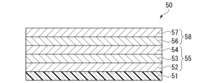
- a laminate 50 having the structure shown in FIG. 5 is created.
- a polyvinylidene fluoride (PVDF) film with a thickness of 50 ⁇ m is prepared as the base material 51, and the surface of this base material 51 is coated with an arithmetic surface roughness Ra of 0.1 ⁇ m and a maximum height Rmax of 1 ⁇ m. Create unevenness.
- a silicon nitride film 52 with a thickness of 200 nm is formed on the base material 51 made of this PVDF film by the CVD method.
- an ethanol solution of tetraethoxysilane is applied onto the silicon nitride film 52, and an 80 nm thick SiOx film 53 is laminated thereon.
- a silicon nitride film 54 is formed on the SiOx film 53, and a base layer 55 consisting of the silicon nitride film 52, the SiOx film 53, and the silicon nitride film 54 is formed.
- a dispersion containing tungsten oxide fine particles (average diameter 10 nm) is applied onto the base layer 55 to create a 50 nm thick tungsten oxide layer 56, and anatase type titanium oxide fine particles are further applied on the tungsten oxide layer 56.
- a titanium oxide layer 57 with a thickness of 70 nm is formed, a photocatalyst layer 58 consisting of a tungsten oxide layer 56 and a titanium oxide layer 57 is formed, and a laminate 50 is obtained.
- the fire resistance of the obtained laminate 50 was evaluated by the UL94V test, the burning time was 4 to 6 seconds, indicating that it has excellent fire resistance.
- Example 4 A solar battery (solar battery cell) 60 shown in FIG. 6 is created.
- a transparent electrode (second electrode) 61 of indium tin oxide (ITO) (200 nm) is created by sputtering.
- a toluene solution of C60-PCBM is applied onto the transparent electrode 61 using a bar coater and dried to form an electron injection layer 62.
- a solution in which lead iodide and methylammonium iodide are dissolved in a solvent is applied onto the electron injection layer 62, and then dried to form the photoelectric conversion layer 63.
- Spiro-OMeTAD 2,2',7,7'-Tetrakis[N,N-di(4-methoxyphenyl)amino]-9,9'-spirobifluorene
- a graphene oxide aqueous solution is applied using a bar coater to form a graphene oxide film.
- the graphene oxide film was dried at 90°C for 20 minutes and then treated with hydrated hydrazine vapor at 110°C for 1 hour to form a two-layer N-graphene film in which some of the carbon atoms in graphene oxide were replaced with nitrogen atoms.
- a shielding layer 66 is formed.
- An aqueous solution of poly(3,4-ethylenedioxythiophene)-poly(styrene sulfonate) (PEDOT/PSS) containing sorbitol was applied on the shielding layer 66 made of N-graphene film, and heated at 100° C.
- the obtained solar cell 60 exhibits an energy conversion efficiency of 10 to 12% for 1 SUN of sunlight, and the efficiency deteriorates by less than 3% even if it is left outdoors for a month. Furthermore, when fire resistance was evaluated using the UL94V test, the combustion time was 5 to 8 seconds, indicating that it has excellent fire resistance.
- Example 5 A solar cell (solar cell) 70 shown in FIG. 7 is created.
- a transparent electrode (second electrode) 71 of ITO (200 nm) is created by sputtering.
- an electron injection layer 72 made of tin oxide is formed by sputtering.
- a solution in which lead iodide and methylammonium iodide are dissolved in a solvent is applied onto the electron injection layer 72, and then dried to form the photoelectric conversion layer 73.
- a solution of Spiro-OMeTAD is applied onto the photoelectric conversion layer 73 and then dried to form a hole transport layer 74.
- a counter transparent electrode (first electrode) 75 of ITO is formed on the hole transport layer 74 by sputtering.
- a resin layer (substrate) 76 is formed by sealing the surface of the opposing transparent electrode 75 made of ITO with transparent polyimide, thereby creating a solar cell 70 having optical transparency.
- the resulting solar cell 70 exhibits an energy conversion efficiency of 8 to 10% for 1 SUN of sunlight, and the efficiency deteriorates by less than 3% even if left outdoors for a month. Furthermore, when fire resistance was evaluated using the UL94V test, the combustion time was 3 to 5 seconds, indicating that it has excellent fire resistance.
- a solar battery (solar battery cell) 80 shown in FIG. 8 is created.
- a transparent electrode (second electrode) 82 of ITO (200 nm) is formed by sputtering on a PVC substrate 81 with a thickness of 100 ⁇ m.
- an electron injection layer 83 of tin oxide is formed by sputtering.
- a solution in which lead iodide and methylammonium iodide are dissolved in a solvent is applied onto the electron injection layer 83, and then dried to form the photoelectric conversion layer 84.
- a solution of Spiro-OMeTAD is applied onto the photoelectric conversion layer 84 and then dried to form a hole transport layer 85.
- a molybdenum (Mo) counter electrode (first electrode) 86 is formed on the hole transport layer 85 by sputtering.
- the surface of the Mo counter electrode 86 is sealed with transparent polyimide to form a resin layer (substrate) 87.
- the laminate 30 obtained in Example 1 is pasted on the surface of the PVC substrate 81 opposite to the transparent electrode 82 (that is, the light receiving side) to create the solar cell 80.
- the obtained solar cell 80 exhibits an energy conversion efficiency of 12 to 15% for 1 SUN of sunlight, and the efficiency deteriorates by less than 3% even if it is left outdoors for a month. Furthermore, when fire resistance was evaluated using the UL94V test, the combustion time was 3 to 5 seconds, indicating that it has excellent fire resistance.
- silicon nitride film 53...SiOx film, 56...Tungsten oxide layer, 57...Titanium oxide layer, 61, 71, 82...transparent electrode (second electrode), 62,72,83...electron injection layer, 64,74,85...hole transport layer, 65...Stainless steel foil electrode (first electrode), 66...shielding layer, 67...adhesive layer, 75... Opposing transparent electrode (first electrode) 76, 87...resin layer (substrate), 81...Substrate 86...Counter electrode (first electrode).
Landscapes
- Physics & Mathematics (AREA)
- Condensed Matter Physics & Semiconductors (AREA)
- Electromagnetism (AREA)
- General Physics & Mathematics (AREA)
- Engineering & Computer Science (AREA)
- Computer Hardware Design (AREA)
- Microelectronics & Electronic Packaging (AREA)
- Power Engineering (AREA)
- Catalysts (AREA)
Abstract
実施形態の太陽電池(1)は、フレキシブル太陽電池シート(10)と、フレキシブル太陽電池シート(10)の受光面上に設けられた積層体(20)と、を備える。積層体(20)は、フレキシブル太陽電池シート(10)の受光面上に配置され、pH7の水中で負のゼータ電位を有する基材(21)と、基材(21)上に配置され、pH7の水中で正のゼータ電位を有する下地層(22)と、下地層(22)上に配置され、光触媒材料を含有し、pH7の水中で負もしくはゼロのゼータ電位を有する光触媒層(23)と、を順に含む。
Description
本発明の実施形態は、太陽電池およびその製造方法に関する。
近年、環境保護及び地球温暖化の防止のために、太陽光発電を利用した太陽電池への期待が高まっている。
従来の太陽電池は、基板や保護膜として比較的厚い(例えば、数mm程度)ガラス板などが使用されていた。そのため、太陽電池自体の重量が重く、耐荷重による制約によって設置可能な場所や設備が限られていた。
そこで近年注目されているのが、薄膜太陽電池である。薄膜太陽電池としては、Si薄膜を用いた薄膜シリコン太陽電池や、銅-インジウム-ガリウム-セレン(CIGS)系薄膜を用いたCIGS系太陽電池、銅-インジウム-硫黄(CIS)系薄膜を用いたCIS系太陽電池などが研究されており、これら太陽電池はいずれも、高い変換効率が期待できる太陽電池として注目されている。
また、上記のような薄膜太陽電池は、樹脂フィルムや金属薄膜上に形成できることから、フレキシブル薄膜太陽電池とも呼ばれている。フレキシブル薄膜太陽電池は、軽量で、且つ、可撓性に優れるため、従来の太陽電池よりも設置場所の制約が少なく、例えば、大型設備の屋根上や曲面を有する場所などに自由に設置することができる。
また、電池セル表面の汚染対策の観点から、受光面に光触媒を含む保護カバーを設けた薄膜太陽電池も検討されている。
しかし、上記のような従来の薄膜太陽電池は、軽量である点で非常に優れる一方、耐候性および耐火性が不十分であり、長時間の利用に耐えうる耐久性が望まれていた。
また、薄膜太陽電池の表面に、汚染対策のために光触媒層を設けた場合、当該光触媒層に隣接する他の層(特に有機膜など)が光触媒によって劣化してしまう問題があった。
さらに、薄膜太陽電池上に、求められる特性に応じた層を積層した場合、各層が剥離しやすいという問題もあった。
また、薄膜太陽電池の表面に、汚染対策のために光触媒層を設けた場合、当該光触媒層に隣接する他の層(特に有機膜など)が光触媒によって劣化してしまう問題があった。
さらに、薄膜太陽電池上に、求められる特性に応じた層を積層した場合、各層が剥離しやすいという問題もあった。
本発明が解決しようとする課題は、耐候性および耐火性に優れ、表面が汚れにくく、かつ、剥がれにくい太陽電池およびその製造方法を提供することである。
実施形態の太陽電池は、フレキシブル太陽電池シートと、前記フレキシブル太陽電池シートの受光面上に設けられた積層体と、を備える。前記積層体は、基材と、下地層と、光触媒層と、を順に含む。前記基材は、前記フレキシブル太陽電池シートの前記受光面上に配置され、pH7の水中で負のゼータ電位を有する。前記下地層は、前記基材上に配置され、pH7の水中で正のゼータ電位を有する。前記光触媒層は、前記下地層上に配置され、光触媒材料を含有し、pH7の水中で負もしくはゼロのゼータ電位を有する。
以下、実施形態の太陽電池およびその製造方法を、図面を参照して説明する。以下の説明では、同一又は類似の機能を有する構成に同一の符号を付す。そして、それら構成の重複する説明は省略する場合がある。図面は模式的又は概念的なものであり、各部分の厚みと幅との関係、部分間の大きさの比率等は、必ずしも現実のものと同一とは限らない。
[第1実施形態]
第1実施形態は、光透過性を有するフレキシブル薄膜太陽電池に関する。
以下、本実施形態のフレキシブル薄膜太陽電池(以下、単に太陽電池と称する場合がある)の構成について説明する。
第1実施形態は、光透過性を有するフレキシブル薄膜太陽電池に関する。
以下、本実施形態のフレキシブル薄膜太陽電池(以下、単に太陽電池と称する場合がある)の構成について説明する。
図1は、第1実施形態に係る太陽電池1の断面概念図を示す。図1に示すように、本実施形態に係る太陽電池1は、フレキシブル太陽電池シート10と、フレキシブル太陽電池シート10の受光面上に設けられた積層体20と、を備える。積層体20は、基材21と、下地層22と、光触媒層23と、を順に含む。なお、本明細書でいう「受光面」とは、フレキシブル太陽電池シート10の表面のうち、太陽光が入射される側の表面を意味する。図1の太陽電池1の場合、フレキシブル太陽電池シート10の上側の表面が「受光面」である。
以下、積層体20の詳細について説明する。なお、フレキシブル太陽電池シート10については、後に詳述する。
以下、積層体20の詳細について説明する。なお、フレキシブル太陽電池シート10については、後に詳述する。
<積層体>
フレキシブル太陽電池シート10の受光面上には、耐候性、耐火性、および汚染を防止するために、基材21と下地層22と光触媒層23とを含む積層体20が設けられる。
フレキシブル太陽電池シート10の受光面上には、耐候性、耐火性、および汚染を防止するために、基材21と下地層22と光触媒層23とを含む積層体20が設けられる。
(基材)
基材21は、フレキシブル太陽電池シート10の受光面上に配置される。基材21は、耐候性および耐火性の観点から、ハロゲン元素を有する樹脂を含んでよく、ハロゲン元素を有する樹脂のみから構成されてもよい。基材21を構成する樹脂としては、難燃性の樹脂であることが好ましい。UL94規格の等級「V-0」以上の難燃性を有する樹脂を用いることがより好ましく、例えば、ポリ塩化ビニル(PVC)、ポリ塩化ビニリデン(PVDC)、ポリフッ化ビニリデン(PVDF)およびポリカーボネート(PC)が挙げられる。これら樹脂を基材21として用いることで、可撓性に優れ、かつ、優れた耐候性と耐火性を有する太陽電池を得ることができる。なお、基材21は、複数の樹脂を組み合わせた複合樹脂であってもよい。
基材21は、フレキシブル太陽電池シート10の受光面上に配置される。基材21は、耐候性および耐火性の観点から、ハロゲン元素を有する樹脂を含んでよく、ハロゲン元素を有する樹脂のみから構成されてもよい。基材21を構成する樹脂としては、難燃性の樹脂であることが好ましい。UL94規格の等級「V-0」以上の難燃性を有する樹脂を用いることがより好ましく、例えば、ポリ塩化ビニル(PVC)、ポリ塩化ビニリデン(PVDC)、ポリフッ化ビニリデン(PVDF)およびポリカーボネート(PC)が挙げられる。これら樹脂を基材21として用いることで、可撓性に優れ、かつ、優れた耐候性と耐火性を有する太陽電池を得ることができる。なお、基材21は、複数の樹脂を組み合わせた複合樹脂であってもよい。
基材21は、pH7の水中で負のゼータ電位を有する。基材21として、ゼータ電位が負である材料を用いることで、正のゼータ電位を有する下地層22との結合力(耐剥離性)を高めることができ、基材21と下地層22との剥離を防止することができる。
ここで「pH7の水中」と規定したのは、通常の大気中での使用を想定しているためであり、例えば、結露や雨水に濡れた場合を想定している。ゼータ電位は、pHを変えると多少は変動するが、急激には変化しにくい。基材21は、pH4~7の範囲内で、負であることが好ましい。なお、ハロゲン元素やカルボニル基を有するポリマーは、負の極性が外側にあるためゼータ電位が負になりやすいことが知られている。
ここで「pH7の水中」と規定したのは、通常の大気中での使用を想定しているためであり、例えば、結露や雨水に濡れた場合を想定している。ゼータ電位は、pHを変えると多少は変動するが、急激には変化しにくい。基材21は、pH4~7の範囲内で、負であることが好ましい。なお、ハロゲン元素やカルボニル基を有するポリマーは、負の極性が外側にあるためゼータ電位が負になりやすいことが知られている。
基材21の膜厚は、特に限定されないが、取り扱い上の観点から、10~100μmの範囲としてよい。好ましくは、30~80μmである。
(下地層)
下地層22は、基材21上に配置される。下地層22は、pH7の水中で正のゼータ電位を有する。これにより、ゼータ電位が負である基材21および光触媒層23それぞれとの結合力を高めることができる。もし、下地層22がない場合、ゼータ電位が負もしくはゼロ(中性)である光触媒層23とゼータ電位が負である基材21とが反発するため、光触媒層23は剥離しやすくなる。つまり、積層体20を構成する各要素の剥離を防止し、より安定した耐久性を得るためには、基材21と光触媒層23との間に、これらとがゼータ電位が異なる下地層22を設けることが効果的である。また、光触媒層23と基材21との間に下地層22を設けることで、光触媒層23と基材21との直接の接触を回避できるため、光触媒作用による基材21の劣化を防ぐことができる。下地層22は、pH4~7の範囲内で、正であることが好ましい。
下地層22は、基材21上に配置される。下地層22は、pH7の水中で正のゼータ電位を有する。これにより、ゼータ電位が負である基材21および光触媒層23それぞれとの結合力を高めることができる。もし、下地層22がない場合、ゼータ電位が負もしくはゼロ(中性)である光触媒層23とゼータ電位が負である基材21とが反発するため、光触媒層23は剥離しやすくなる。つまり、積層体20を構成する各要素の剥離を防止し、より安定した耐久性を得るためには、基材21と光触媒層23との間に、これらとがゼータ電位が異なる下地層22を設けることが効果的である。また、光触媒層23と基材21との間に下地層22を設けることで、光触媒層23と基材21との直接の接触を回避できるため、光触媒作用による基材21の劣化を防ぐことができる。下地層22は、pH4~7の範囲内で、正であることが好ましい。
下地層22は、無機化合物を含むことが好ましい。無機化合物としては、アルミニウム酸化物、ジルコニウム酸化物などの無機酸化物、もしくは、窒化ケイ素等の無機窒化物が挙げられる。下地層22としてこれら無機化合物を用いることで、光触媒作用による基材21の劣化を防ぎ、かつ、下地層23のゼータ電位を正に調整することができる。これら無機化合物の中でも、アルミニウム酸化物および窒化ケイ素が好ましい。アルミニウム酸化物および窒化ケイ素は、広いpH範囲でゼータ電位が正であり、かつ、外部からの水分の侵入を防止する作用を有する。そのため、下地層22の材料としてより好適である。つまり、アルミニウム酸化物もしくは窒化ケイ素を含む下地層22を設けることで、水蒸気を透過させにくくなり、太陽電池の光電変換層13(図2参照)の劣化を防止することができる。これらの膜を積層膜や複合膜として用いてもよい。なお、下地層22としてアルミニウム酸化物の膜(AlOx膜)を用いる場合、AlOx膜は化学当量から外れていてもよいしアルキル基が含まれていれもよい。
アルミニウム酸化物としては、アルミナ水和物を使用することができる。アルミナ水和物はAl2O3・(H2O)x(0<x<=3)で表わされる水和物であり、種々の形態がある。中でも、ベーマイト(x=1)もしくは擬ベーマイト(1<x<2)であることが好ましい。ベーマイトおよび擬ベーマイトは、塗布乾燥により容易に丈夫な塗布膜を形成でき、かつ、pH7の水中で正に帯電しやすい。
下地層22は、前述の無機化合物と有機ポリマーの積層構造、または前述の無機化合物と無機酸化物との積層構造であってもよい。これらの場合、有機ポリマーまたは無機酸化物は、無機化合物との間に挟まれた構造が好ましい。これにより下地層22は、pH7で正に帯電しやすい形態とできる。有機ポリマーや無機酸化物はpH7で負に帯電しやすいと、積層構造が安定化するとともに、バリア性能も向上しやすい。
下地層23の膜厚は、特に限定されないが、均一性の観点から、0.1~10μmの範囲としてよい。好ましくは、0.2~2μmである。
(光触媒層)
光触媒層23は、光触媒材料を含有し、下地層22上に配置される。光触媒層23は、光触媒層23に含まれる光触媒材料は、光触媒作用を高める観点から、酸化チタンもしくは酸化タングステンが挙げられる。
光触媒層23は、光触媒材料を含有し、下地層22上に配置される。光触媒層23は、光触媒層23に含まれる光触媒材料は、光触媒作用を高める観点から、酸化チタンもしくは酸化タングステンが挙げられる。
本実施形態における「光触媒作用」とは、アンモニア、アルデヒド類等の有害物質の分解、抗菌作用、抗ウイルス作用、また汚れが付着しにくい防汚作用をいう。酸化チタンおよび酸化タングステンは、この光触媒作用に優れることから、好適に用いられる。耐紫外線に対しては、酸化チタンがより有効であるため、太陽電池1の使用環境が屋外である場合には、酸化チタンを用いることがより好ましい。
なお、光触媒層23は、酸化チタンもしくは酸化タングステンのみから構成されてもよいが、これら材料が積層されたり、複合されたりしてもよい。また、光触媒層23は、助触媒材料をさらに含んでもよい。
光触媒層23は、pH7の水中で負もしくはゼロのゼータ電位を有する。基材21として、ゼータ電位が負もしくはゼロである光触媒材料を用いることで、正のゼータ電位を有する下地層22との結合力(耐剥離性)を高めることができ、光触媒層23と下地層22との剥離を防止することができる。なお、「ゼロのゼータ電位」とは、光触媒材料が電気的に中性である状態を意味する。光触媒層23は、pH4~7の範囲内で、負もしくはゼロであることが好ましい。
光触媒層23に助触媒材料をさらに含む場合は、助触媒材料は、正のゼータ電位を有することが好ましい。正のゼータ電位を有する助触媒材料は、例えば、酸化鉄、酸化ニッケル、酸化銅、これらの複合酸化物等が挙げられる。
光触媒層23が、異なるゼータ電位を有する光触媒材料と助触媒材料とを含むことにより、光触媒層23の光触媒活性が上がる傾向がある。これは、助触媒材料のゼータ電位が正に帯電していると、ゼータ電位が負もしくはゼロの光触媒材料との結合が強くなるためである。また、下地層22はゼータ電位が正に帯電しているため、ゼータ電位が正に帯電している助触媒材料が下地層22と反発することで、光触媒材料と結合しやすくなり、結果、光触媒活性を向上できる。
光触媒材料として、4nm~200nmの体積平均粒子径を有する光触媒粒子を使用することができる。体積平均粒子径がこの範囲内であると、分散液の安定性、下地層22に塗布する際の加工性、及び光触媒機能が良好となる傾向がある。体積平均粒子径はより好ましくは10nmから100nmであり、さらに好ましくは20nmから50nmである。
光触媒層23の表面の算術平均粗さRaは、0.1~1.0μmとしてもよい。太陽電池の効率を高めるには、太陽電池(セル)表面での反射率を低減することが有効である。当該反射率を低減させる方法として、例えば、セル表面に反射防止膜を設ける方法があるが、セル表面に凹凸を付与する方法も有効である。セル表面に凹凸を付与することで、太陽光の反射を抑制でき、より多くの太陽光をセル内に取り込むことができる。この効果を十分に得るためには、光触媒層23の表面の算術平均粗さRaは、0.1~1.0μmとするとよい。光触媒層23の表面の算術平均粗さRaが小さすぎると、太陽光の反射抑制効果を十分に得られないおそれがある。一方、光触媒層23の表面の算術平均粗さRaが大きすぎると、セル表面に付着した汚染が取れなくなるおそれがある。これらのことから、光触媒層23の表面の算術平均粗さRaは、0.2~0.8μmとすることがより好ましい。光触媒層23の表面に凹凸を形成するためには、光触媒層23の下方に設ける基材21にあらかじめサンドブラスト等で凹凸をつけることが好ましい。予め基材21に凹凸を設けておくことで、基材21の上方に設ける光触媒層23の表面も付随的に凹凸が設けられることとなる。
上記と同様の観点から、光触媒層23の表面の最大高さRmaxは、1~10μmとしてもよい。光触媒層23の表面の最大高さRmaxを当該範囲内とすることで、太陽光の反射を抑制でき、より多くの太陽光をセル内に取り込むことができる。光触媒層23の表面の最大高さRmaxは、2~8μmとすることがより好ましい。
光触媒層23の表面の算術平均粗さRaおよび最大高さRmaxは、以下の方法により求めることができる。
算術表面粗さRaおよび最大高さRmaxはいずれも、ダイヤモンド針を接触させて掃引する触針走査法で測定することができる。
まず、粗さ曲線(長さ4mm程度)からその平均線の方向に基準長さ(0.8mm)を抜き取り、この抜き取り部分の平均線の方向をX軸、縦倍率の方向をY軸と設定する。粗さ曲線をy=f(x)で表したとき、以下の式(1)によって求められる値をマイクロメートル(μm)で表したものを算術平均粗さRaとする。

また、粗さ曲線(長さ4mm程度)から傷等の欠陥部分を除いた基準長さ(0.8mm)を抜き取り、この抜き取り部分の平均線に平行な2直線で抜き取り部分をはさんだとき、2直線の間隔を断面曲線の縦倍率の方向に計測して、その値をマイクロメートル単位(μm)で表したものを抜き取り部分の最大高さRmaxとする。つまり、抜き取り部分のうち、縦倍率の方向(Y軸方向)における最も高い部分と最も低い部分の高さの差を最大高さRmaxとする。
光触媒層23の膜厚は、特に限定されないが、活性の観点から、20~1000nmの範囲としてよい。好ましくは、40~800nmである。
以上、第1実施形態に係る積層体20について説明した。
ここで、本実施形態における基材21、下地層22および光触媒層23のゼータ電位は、「ゼータサイザーナノZS」(マルバーン社製)を用い、電気泳動光散乱法(ELS)により測定できる。具体的には、平板ゼータ電位測定用セルによって、トレーサー粒子としてポリスチレンラテックスを用いて測定する。
ここで、本実施形態における基材21、下地層22および光触媒層23のゼータ電位は、「ゼータサイザーナノZS」(マルバーン社製)を用い、電気泳動光散乱法(ELS)により測定できる。具体的には、平板ゼータ電位測定用セルによって、トレーサー粒子としてポリスチレンラテックスを用いて測定する。
基材21、下地層22および光触媒層23のゼータ電位を測定するときのpHは、純水に希塩酸と希水酸化カリウム水溶液を添加することで調整できる。
また、用いる材料が粉末状(例えば、光触媒材料や助触媒材料など)である場合も同様に、測定対象物のゼータ電位は、「ゼータサイザーナノZS」(マルバーン社製)を用い、電気泳動光散乱法(ELS)により測定できる。このとき用いるセルは、キャピラリーセルとする。
用いる材料が粉末状である場合、ゼータ電位を測定するときのpHは、例えば、光触媒材料(もしくは助触媒材料)を分散させた純水に希塩酸と希水酸化カリウム水溶液を添加することで調整できる。
以上、本実施形態に係る積層体20の詳細を説明した。
図1に示すように、第1実施形態の太陽電池1は、フレキシブル太陽電池シート10上に上記の積層体20が設けられた構成を有する。本実施形態では、フレキシブル太陽電池シート10の形態は特に限定されず、種々の太陽電池が適用可能である。つまり、太陽電池の種類や形態が制限されることなく、上記の積層体20を設けることができる。
以上説明した第1実施形態の太陽電池1によれば、基材21のゼータ電位が負に帯電し、下地層22のゼータ電位が正に帯電し、かつ光触媒層23のゼータ電位が負もしくはゼロに帯電することにより、各層の間が強固に固定され、剥離等が起きにくい。
また、第1実施形態の太陽電池1は、フレキシブル太陽電池シート1側から順に、基材21、下地層22および光触媒層23を有するため、光触媒材料による基材21(例えば樹脂)の劣化を防ぎながら、耐候性および耐火性を高めることができる。そのため、屋外での長時間の利用にも耐えうる太陽電池を提供することができる。
また、第1実施形態の太陽電池1は、フレキシブル太陽電池シート1側から順に、基材21、下地層22および光触媒層23を有するため、光触媒材料による基材21(例えば樹脂)の劣化を防ぎながら、耐候性および耐火性を高めることができる。そのため、屋外での長時間の利用にも耐えうる太陽電池を提供することができる。
また、第1実施形態の太陽電池1を構成する積層体20の全体形状は、シート状(フィルム状)であることが好ましい。これにより、可撓性に優れたフレキシブル薄膜太陽電池を得ることができる。
また、第1実施形態の積層体20を構成する各層の形成方法は、特に限定されず、CVD法、真空蒸着法、スパッタリング法、イオンプレーティング法、メッキ法、塗布法、ゾルゲル法等で形成されてよい。中でも、CVD(Chemical Vapor Deposition)法は、水蒸気バリア性の高い層を形成できる点で好ましい。また、下地層22および光触媒層23は、粒子分散液やゾルゲル法の前駆体液を塗布することにより形成されてもよい。これにより、安価でかつ安定して積層体20を構成する各層を製造することができる。なお、粒子分散液を用いる場合、溶媒として、水、もしくは水-アルコール混合液が適用可能である。溶媒として水を用いた水分散液の場合は、分散液に界面活性材を加えてもよい。
[第2実施形態]
次に、第1実施形態の積層体20が設けられるフレキシブル太陽電池シートの好ましい形態を説明する。
次に、第1実施形態の積層体20が設けられるフレキシブル太陽電池シートの好ましい形態を説明する。
図2は、第2実施形態に係る太陽電池1Aの断面概念図を示す。図2に示すように、本実施形態に係る太陽電池1Aは、フレキシブル太陽電池シート10Aと、フレキシブル太陽電池シート10Aの受光面上に設けられた積層体20と、を備える。
<フレキシブル太陽電池シート>
フレキシブル太陽電池シート10Aは、受光面とは反対側から順に、基板11と、第1電極12と、光電変換層13と、第2電極14と、を備える。なお、第1電極12と光電変換層13との間や、光電変換層13と第2電極14との間には、図示しない中間層(例えば、正孔輸送層および電子注入層など)が含まれていてもよい。また、第2電極14上(つまり、第2電極14と積層体20との間)に、図示しない保護層または他の基板が設けられていてもよい。
以下、フレキシブル太陽電池シート(以下、太陽電池シートとも称する)10Aについて詳述する。
フレキシブル太陽電池シート10Aは、受光面とは反対側から順に、基板11と、第1電極12と、光電変換層13と、第2電極14と、を備える。なお、第1電極12と光電変換層13との間や、光電変換層13と第2電極14との間には、図示しない中間層(例えば、正孔輸送層および電子注入層など)が含まれていてもよい。また、第2電極14上(つまり、第2電極14と積層体20との間)に、図示しない保護層または他の基板が設けられていてもよい。
以下、フレキシブル太陽電池シート(以下、太陽電池シートとも称する)10Aについて詳述する。
(基板)
基板11としては、特に限定されないが、可撓性を確保するために、ポリエチレンテレフタレート(PET)、ポリエチレンナフタレート(PEN)、ポリ塩化ビニル(PVC)、ポリカーボネート(PC)、ポリフッ化ビニリデン(PVDF)、ポリ塩化ビニリデン(PVDC)、ポリイミド、アクリル等の樹脂を用いることが好ましい。基板1の厚みは、例えば、50μm~200μmである。
基板11としては、特に限定されないが、可撓性を確保するために、ポリエチレンテレフタレート(PET)、ポリエチレンナフタレート(PEN)、ポリ塩化ビニル(PVC)、ポリカーボネート(PC)、ポリフッ化ビニリデン(PVDF)、ポリ塩化ビニリデン(PVDC)、ポリイミド、アクリル等の樹脂を用いることが好ましい。基板1の厚みは、例えば、50μm~200μmである。
(第1電極)
第1電極12は、基板11と光電変換層13の間に設けられる。第1電極12は金属膜であってもよいし、透明電極であってもよい。透明電極の場合は積層膜であることが好ましい。例えば、光電変換層13側の第1層としてSnを主成分とする酸化物透明導電膜を設け、基板11側の第2層として、第1層よりも低抵抗な透明導電膜を設けることが好ましい。積層膜が好ましい理由は、第1層であるSnを主成分とする酸化物透明導電膜の抵抗率が、第2層と比較して高いため、第1層を単独で用いると、抵抗成分による発電損失が大きいためである。
第1電極12は、基板11と光電変換層13の間に設けられる。第1電極12は金属膜であってもよいし、透明電極であってもよい。透明電極の場合は積層膜であることが好ましい。例えば、光電変換層13側の第1層としてSnを主成分とする酸化物透明導電膜を設け、基板11側の第2層として、第1層よりも低抵抗な透明導電膜を設けることが好ましい。積層膜が好ましい理由は、第1層であるSnを主成分とする酸化物透明導電膜の抵抗率が、第2層と比較して高いため、第1層を単独で用いると、抵抗成分による発電損失が大きいためである。
第1層としては、SnO2など、Snを主成分とする酸化物が好ましい。必要に応じて、第1層に添加物が含まれてもよい。添加物は限定されないが、Zn、Al、Ga、In、Si、Ge、Ti、Cu、Sb、Nb、FおよびTaなどが挙げられる。
第2層としては、例えば、酸化インジウムスズ(Indium Tin Oxide:ITO)、アルミニウムドープ酸化亜鉛(Al-doped Zinc Oxide:AZO)、ボロンドープ酸化亜鉛(Boron-doped Zinc Oxide:BZO)、ガリウムドープ酸化亜鉛(Gallium-doped Zinc Oxide:GZO)、インジウムドープ酸化亜鉛(Indium-doped Zinc Oxide:IZO)、チタンドープ酸化インジウム(Titanium-doped Indium Oxide:ITiO)や酸化インジウムガリウム亜鉛(IndiumGallium Zinc Oxide:IGZO)、水素ドープ酸化インジウム(Hydrogen-doped Indium Oxide:In2O3)などを用いることができ、特に限定されない。透明導電膜は、積層膜であってもよく、上記酸化物の他に酸化スズなどの膜が積層膜に含まれていてもよい。また、第1電極12は、透明導電膜、金属膜を積層したものを用いることもできる。金属膜を4nm~20nmの厚さにすることにより透明電極として用いることができる。透明導電膜については先述したとおりだが、金属膜としては、Al、Ag、ステンレス、Mo、AuやWの膜など特に限定されない。
第1電極12は、真空蒸着法、スパッタリング法、イオンプレーティング法、メッキ法、塗布法等で形成される。第1電極12の厚みは、用いる材料に応じて適宜決定されてよいが、例えば、50nm~250nmであることが好ましい。
(光電変換層)
光電変換層13は、入射した太陽光により起電するものであれば特に限定されないが、ペロブスカイト構造を有する材料(ペロブスカイト系化合物)を用いることができる。好ましくは、ハロゲン元素を有するペロブスカイト系化合物である。
光電変換層13は、入射した太陽光により起電するものであれば特に限定されないが、ペロブスカイト構造を有する材料(ペロブスカイト系化合物)を用いることができる。好ましくは、ハロゲン元素を有するペロブスカイト系化合物である。
ペロブスカイト構造は、例えばイオンA1、イオンA2、およびイオンXからなり、A1A2X3と表すことができる。イオンA2がイオンA1に比べて小さい場合にペロブスカイト構造を有する場合がある。ペロブスカイト構造は、例えば立方晶系の単位格子をもつ。立方晶の各頂点にイオンA1が配置され、体心にイオンA2が配置される。体心のイオンA2を中心として立方晶の各面心にイオンXが配置される。
A2X6八面体の向きは、イオンA1との相互作用によって、歪みやすい。対称性の低下により、モット転移が生じ、イオンMに局在していた価電子がバンドとして広がることができる。イオンA1は、CH3NH3であることが好ましい。イオンA2は、PbおよびSnの少なくともいずれかであることが好ましい。イオンXは、Cl、Br、およびIの少なくともいずれかであることが好ましい。イオンA1、イオンA2、およびイオンXを構成する材料のそれぞれは、単一の材料であっても混合された材料であっても良い。光電変換層13の厚さは、例えば、200nm~800nmである。
光電変換層を形成する際は、材料を溶媒に溶解し、電極(または中間層)上に塗布する塗布法を採用するとよい。用いる溶媒としては、例えば、不飽和炭化水素系溶媒、ハロゲン化芳香族炭化水素系溶媒、ハロゲン化飽和炭化水素系溶媒、エーテル類等が挙げられる。不飽和炭化水素系溶媒としては、トルエン、キシレン、テトラリン、デカリン、メシチレン、n-ブチルベンゼン、sec-ブチルベンゼン、tert-ブチルベンゼン等が挙げられる。ハロゲン化芳香族炭化水素系溶媒としては、クロロベンゼン、ジクロロベンゼン、トリクロロベンゼン等が挙げられる。ハロゲン化飽和炭化水素系溶媒としては、四塩化炭素、クロロホルム、ジクロロメタン、ジクロロエタン、クロロブタン、ブロモブタン、クロロペンタン、クロロヘキサン、ブロモヘキサン、クロロシクロヘキサン等が挙げられる。エーテル類としては、テトラヒドロフラン、テトラヒドロピラン等が挙げられる。ハロゲン系の芳香族溶剤を用いることが、より好ましい。さらにDMF(N,N-ジメチルホルムアミド)、DMSO(ジメチルスルホキシド)、2-プロパノール、γ-ブチロラクトンを用いることもできる。これらの溶剤を単独、もしくは混合して使用することが可能である。材料を溶解できる溶媒であれば特に制約されない。
溶液を塗布し、光電変換層を形成する方法としては、スピンコート法、ディップコート法、キャスティング法、バーコート法、ロールコート法、ワイアーバーコート法、スプレー法、スクリーン印刷、グラビア印刷法、フレキソ印刷法、オフセット印刷法、グラビア・オフセット印刷、ディスペンサー塗布、ノズルコート法、キャピラリーコート法、インクジェット法、メニスカス塗布法等が挙げられる。これらの塗布法を単独で、もしくは組み合わせて用いることができる。
(第2電極)
第2電極14は、透明導電材料を含むことが好ましい。本実施形態の第2電極14は、第1電極12と同様の材料を用いることができる。第2電極14は、第1電極12と同様に、真空蒸着法、スパッタリング法、イオンプレーティング法、メッキ法、塗布法等で形成される。
第2電極14は、透明導電材料を含むことが好ましい。本実施形態の第2電極14は、第1電極12と同様の材料を用いることができる。第2電極14は、第1電極12と同様に、真空蒸着法、スパッタリング法、イオンプレーティング法、メッキ法、塗布法等で形成される。
以上、第2実施形態に係る太陽電池1Aを説明した。
第2実施形態に係る太陽電池1Aによれば、第1実施形態と同様に、耐候性および耐火性に優れ、耐久性の高いフレキシブル薄膜太陽電池を提供できる。
第2実施形態に係る太陽電池1Aによれば、第1実施形態と同様に、耐候性および耐火性に優れ、耐久性の高いフレキシブル薄膜太陽電池を提供できる。
なお、第2実施形態に係る太陽電池シート10Aを構成する各層の構成、厚みおよび組成などは、上記効果を阻害しない範囲内で、適宜変更されても構わない。
また、上述したように、太陽電池シート10Aと積層体20との間には保護膜等が設けられてもよいし、太陽電池シート10Aと積層体20とが直接接触されてもよい。つまり、図2に示すように、太陽電池1Aは、基材21と第2電極14とが接するように構成されても構わない。
以上説明した少なくともひとつの実施形態によれば、太陽電池は、フレキシブル太陽電池シートと、フレキシブル太陽電池シートの受光面上に設けられた積層体と、をもつ。積層体は、フレキシブル太陽電池シートの受光面上に配置され、pH7の水中で負のゼータ電位を有する基材と、基材上に配置され、pH7の水中で正のゼータ電位を有する下地層と、下地層上に配置され、光触媒材料を含有し、pH7の水中で負もしくはゼロのゼータ電位を有する光触媒層と、を順に含む。このような構成によれば、耐候性および耐火性に優れ、表面が汚れにくく、かつ、剥がれにくい太陽電池を提供できる。
以下、実施例によって本実施形態をより具体的に説明するが、実施例での条件は本実施形態の実施可能性および効果を確認するために採用した例に過ぎず、本実施形態はこの条件例に限定されるものではない。本実施形態は、本実施形態の要旨を逸脱せず、本実施形態の目的を達成する限りにおいて、種々の条件を採用し得るものである。
(実施例1)
図3に示す構造を有する積層体30を作成する。
まず、基材31として、厚さ50μmのポリ塩化ビニル(PVC)フィルムを準備し、この基材31表面に、サンドブラスト法で、算術平均粗さRaが0.2μm、最大高さRmaxが3μmの凹凸をつける。
次いで、このPVCフィルムからなる基材31上に、トリイソプロポキシアルミニウムのイソプロパノール溶液を塗布し、さらに80℃で加熱乾燥することで100nmのAlOx膜32を作成する。AlOx膜32のpH7の水中でのゼータ電位は正である。
次に、AlOx膜32上に、ポリフッ化ビニリデン(PVDF)のDMF(N,N-ジメチルホルムアミド)溶液を塗布し、膜厚100nmのポリフッ化ビニリデン(PVDF)膜33を積層する。
さらにPVDF膜33の上にAlOx膜34を作成し、AlOx膜32、PVDF膜33およびAlOx膜34からなる下地層35を作成する。
下地層35の上に、テトラエトキシチタンのエタノール溶液を塗布し、厚さ40nmのTiOxからなる光触媒層36を成膜し、積層体30を作成する。TiOxのpH7のゼータ電位は若干負である。
得られる積層体30について、UL94V試験(垂直燃焼性試験)によって耐火性を評価すると、燃焼時間は5~7秒であり、優れた耐火性を示す。
(実施例2)
図4に示す構造を有する積層体40を作成する。
まず、基材41として、厚さ60μmのポリカーボネート(PC)フィルムを準備し、この基材41表面に、サンドブラスト法で、算術平均粗さRaが0.3μm、最大高さRmaxが5μmの凹凸をつける。
次いで、このPCフィルムからなる基材41上に、CVD法で厚さ200nmの窒化ケイ素膜42を作成する。窒化ケイ素膜42のpH7の水中でのゼータ電位は正である。
次に、窒化ケイ素膜42上に、ポリフッ化ビニリデン(PVDF)のDMF溶液を塗布し、膜厚100nmのポリフッ化ビニリデン(PVDF)膜43を積層する。
さらにPVDF膜43の上に窒化ケイ素膜44を作成し、窒化ケイ素膜42、PVDF膜43および窒化ケイ素膜44からなる下地層45を作成する。
下地層45の上に、アナターゼ型の酸化チタンの微粒子(平均径8nm)を含む分散液を塗布し、厚さ80nmの光触媒層46を成膜し、積層体40を作成する。酸化チタン微粒子からなる光触媒層46のpH7の水中でのゼータ電位は0から若干正である。
得られる積層体40について、UL94V試験によって耐火性を評価すると、燃焼時間は8~10秒であり、耐火性に優れる。
(実施例3)
図5に示す構造を有する積層体50を作成する。
まず、基材51として、厚さ50μmのポリフッ化ビニリデン(PVDF)フィルムを準備し、この基材51表面に、サンドブラスト法で、算術表面粗さRaが0.1μm、最大高さRmaxが1μmの凹凸をつける。
次いで、このPVDFフィルムからなる基材51上に、CVD法で厚さ200nmの窒化ケイ素膜52を作成する。
次に、窒化ケイ素膜52上に、テトラエトキシシランのエタノール溶液を塗布し、膜厚80nmのSiOx膜53を積層する。
さらにSiOx膜53の上に窒化ケイ素膜54を作成し、窒化ケイ素膜52、SiOx膜53および窒化ケイ素膜54からなる下地層55を作成する。
下地層55の上に、酸化タングステン微粒子(平均径10nm)を含む分散液を塗布し、厚さ50nmの酸化タングステン層56を作成し、さらに、酸化タングステン層56の上にアナターゼ型の酸化チタン微粒子(平均径8nm)を含む分散液を塗布し、厚さ70nmの酸化チタン層57を成膜し、酸化タングステン層56と酸化チタン層57とからなる光触媒層58を形成し、積層体50を得る。
得られる積層体50について、UL94V試験によって耐火性を評価すると、燃焼時間は4~6秒であり、耐火性に優れる。
(実施例4)
図6に示す太陽電池(太陽電池セル)60を作成する。
実施例2で得られた積層体40のPCフィルム(基材41)上に、酸化インジウムスズ(Indium Tin Oxide:ITO)(200nm)の透明電極(第2電極)61をスパッタで作成する。この透明電極61の上にC60-PCBMのトルエン溶液をバーコーターで塗布して乾燥させ、電子注入層62を形成する。
次に、電子注入層62上に、ヨウ化鉛とメチルアンモニウムヨウ化物を溶媒に溶解させた溶液を塗布し、その後、乾燥させて光電変換層63を作製する。次いで、光電変換層63の上に、2,2’,7,7’-Tetrakis[N,N-di(4-methoxyphenyl)amino]-9,9’-spirobifluorene(以下、Spiro-OMeTADという)の溶液を塗布し、その後乾燥させて正孔輸送層64を作製する。
次に、絶縁性セラミックス膜が反対面(受光面とは反対側の面)に形成されたステンレス箔電極(第1電極)65の受光側の表面に、当該表面を希塩酸で処理して表面酸化膜を除去してから、酸化グラフェンの水溶液をバーコーターで塗布して酸化グラフェン膜を形成させる。次いで、酸化グラフェン膜を90℃で20分乾燥した後、110℃の水和ヒドラジン蒸気で1時間処理し、酸化グラフェンの炭素原子の一部が窒素原子に置換された2層N-グラフェン膜からなる遮蔽層66を形成する。
N-グラフェン膜からなる遮蔽層66の上に、ソルビトールを含有したポリ(3,4-エチレンジオキシチオフェン)-ポリ(スチレンスルホネート)(PEDOT・PSS)の水溶液を塗布し、100℃で30分乾燥して、PEDOT・PSSを含む接着層67(50nm厚)を形成させる。
その後、接着層67と正孔輸送層64を貼り合わせて太陽電池セル60を得る。
得られた太陽電池60は、1SUNの太陽光に対して10~12%のエネルギー変換効率を示し、室外で一か月放置しても効率の劣化は3%未満である。またUL94V試験によって耐火性を評価すると、燃焼時間は5~8秒であり、耐火性にも優れる。
(実施例5)
図7に示す太陽電池(太陽電池セル)70を作成する。
実施例3で得られた積層体50のPVDFフィルム(基材51)上に、ITO(200nm)の透明電極(第2電極)71をスパッタで作成する。この透明電極71の上に、スパッタで酸化スズからなる電子注入層72を形成する。
次に、電子注入層72上に、ヨウ化鉛とメチルアンモニウムヨウ化物を溶媒に溶解させた溶液を塗布し、その後乾燥させて、光電変換層73を作製する。次いで、光電変換層73の上に、Spiro-OMeTADの溶液を塗布し、その後乾燥させて正孔輸送層74を作製する。
次に、正孔輸送層74の上に、ITOの対向透明電極(第1電極)75をスパッタで作成する。ITOの対向透明電極75の表面を透明ポリイミドで封止して樹脂層(基板)76を形成させて、光透過性を有する太陽電池70を作成する。
得られる太陽電池70は、1SUNの太陽光に対して8~10%のエネルギー変換効率を示し、室外で一か月放置しても効率の劣化は3%未満である。またUL94V試験によって耐火性を評価すると、燃焼時間は3~5秒であり、耐火性にも優れる。
(実施例6)
図8に示す太陽電池(太陽電池セル)80を作成する。
まず、厚さ100μmのPVCの基板81上に、ITO(200nm)の透明電極(第2電極)82をスパッタで作成する。この透明電極82の上に、スパッタで酸化スズの電子注入層83を形成する。
次に、電子注入層83上に、ヨウ化鉛とメチルアンモニウムヨウ化物を溶媒に溶解させた溶液を塗布し、その後乾燥させて、光電変換層84を作製する。次いで、光電変換層84の上に、Spiro-OMeTADの溶液を塗布し、その後乾燥させて正孔輸送層85を作製する。
次に、正孔輸送層85の上に、スパッタでモリブデン(Mo)の対向電極(第1電極)86を作成する。Moの対向電極86の表面を透明ポリイミドで封止して樹脂層(基板)87を形成させる。
PVCの基板81の透明電極82とは反対側(つまり受光側)の表面上に、実施例1で得られた積層体30を貼り付けて太陽電池80を作成する。
得られた太陽電池80は、1SUNの太陽光に対して12~15%のエネルギー変換効率を示し、室外で一か月放置しても効率の劣化は3%未満である。またUL94V試験によって耐火性を評価すると、燃焼時間は3~5秒であり、耐火性にも優れる。
1,1A,60,70,80…太陽電池、
10…フレキシブル太陽電池シート、
11…基板、
12…第1電極、
13,63,73,84…光電変換層、
14…第2電極、
20,30,40,50…積層体、
21,31,41,51…基材、
22,35,45,55…下地層、
23,36,46,58…光触媒層、
32,34…AlOx膜、
33,43…PVDF膜、
42,44,52,54…窒化ケイ素膜、
53…SiOx膜、
56…酸化タングステン層、
57…酸化チタン層、
61,71,82…透明電極(第2電極)、
62,72,83…電子注入層、
64,74,85…正孔輸送層、
65…ステンレス箔電極(第1電極)、
66…遮蔽層、
67…接着層、
75…対向透明電極(第1電極)
76,87…樹脂層(基板)、
81…基板
86…対向電極(第1電極)。
Claims (20)
- フレキシブル太陽電池シートと、
前記フレキシブル太陽電池シートの受光面上に設けられた積層体と、
を備え、
前記積層体は、
前記フレキシブル太陽電池シートの前記受光面上に配置され、pH7の水中で負のゼータ電位を有する基材と、
前記基材上に配置され、pH7の水中で正のゼータ電位を有する下地層と、
前記下地層上に配置され、光触媒材料を含有し、pH7の水中で負もしくはゼロのゼータ電位を有する光触媒層と、
を順に含む、太陽電池。 - 前記積層体の形状がフィルム状である、請求項1に記載の太陽電池。
- 前記基材は、樹脂を含む、請求項1または2に記載の太陽電池。
- 前記基材は、ハロゲン元素を有する樹脂を含む、請求項1または2に記載の太陽電池。
- 前記樹脂は、ポリ塩化ビニル、ポリ塩化ビニリデンもしくはポリフッ化ビニリデンである、請求項4に記載の太陽電池。
- 前記樹脂は、ポリカーボネートである、請求項3に記載の太陽電池。
- 前記下地層は、無機化合物を含む、請求項1~3の何れか一項に記載の太陽電池。
- 前記無機化合物は、酸化アルミニウムもしくは窒化ケイ素である、請求項7に記載の太陽電池。
- 前記下地層は、前記無機化合物に挟持された有機ポリマーもしくは無機酸化物を有する請求項7または8に記載の太陽電池。
- 前記有機ポリマーもしくは前記無機酸化物が、pH7の水中で負のゼータ電位を有する請求項9に記載の太陽電池。
- 前記光触媒層は、酸化チタンもしくは酸化タングステンを含む、請求項1~10の何れか一項に記載の太陽電池。
- 前記光触媒層の表面の算術平均粗さRaが、0.1~1.0μmである、請求項1~11の何れか一項に記載の太陽電池。
- 前記光触媒層の表面の最大高さRmaxが、1~10μmである、請求項1~12の何れか一項に記載の太陽電池。
- 前記フレキシブル太陽電池シートは、前記受光面とは反対側から順に、
基板と、
第1電極と、
光電変換層と、
第2電極と、
を備え、
前記光電変換層は、ハロゲン元素を有するペロブスカイト化合物を含む、請求項1から13の何れか一項に記載の太陽電池。 - 前記第2電極は、透明導電材料を含む、請求項14に記載の太陽電池。
- 前記基材と前記第2電極とが接している、請求項14または15に記載の太陽電池。
- 請求項1に記載の太陽電池を製造する方法であって、
前記光触媒層および/もしくは前記下地層を、粒子分散液を塗布することにより形成する、太陽電池の製造方法。 - 請求項1に記載の太陽電池を製造する方法であって、
前記光触媒層および/もしくは前記下地層を、ゾルゲル法の前駆体液を塗布することにより形成する、太陽電池の製造方法。 - 請求項1に記載の太陽電池を製造する方法であって、
前記光触媒層および/もしくは前記下地層を、スパッタにより形成する、太陽電池の製造方法。 - 請求項14に記載の太陽電池を製造する方法であって、
前記下地層とは反対側の前記基材上に前記第2電極を形成する、太陽電池の製造方法。
Priority Applications (1)
| Application Number | Priority Date | Filing Date | Title |
|---|---|---|---|
| PCT/JP2022/023471 WO2023238391A1 (ja) | 2022-06-10 | 2022-06-10 | 太陽電池およびその製造方法 |
Applications Claiming Priority (1)
| Application Number | Priority Date | Filing Date | Title |
|---|---|---|---|
| PCT/JP2022/023471 WO2023238391A1 (ja) | 2022-06-10 | 2022-06-10 | 太陽電池およびその製造方法 |
Publications (1)
| Publication Number | Publication Date |
|---|---|
| WO2023238391A1 true WO2023238391A1 (ja) | 2023-12-14 |
Family
ID=89117860
Family Applications (1)
| Application Number | Title | Priority Date | Filing Date |
|---|---|---|---|
| PCT/JP2022/023471 WO2023238391A1 (ja) | 2022-06-10 | 2022-06-10 | 太陽電池およびその製造方法 |
Country Status (1)
| Country | Link |
|---|---|
| WO (1) | WO2023238391A1 (ja) |
Citations (9)
| Publication number | Priority date | Publication date | Assignee | Title |
|---|---|---|---|---|
| JP2000031509A (ja) * | 1998-07-16 | 2000-01-28 | Dainippon Printing Co Ltd | 太陽電池モジュール |
| JP2000208791A (ja) * | 1999-01-13 | 2000-07-28 | Dainippon Printing Co Ltd | 太陽電池モジュ―ル用表面保護シ―トおよびそれを使用した太陽電池モジュ―ル |
| JP2001328201A (ja) * | 2000-03-14 | 2001-11-27 | Toshiba Lighting & Technology Corp | 光触媒体、光触媒体の製造方法、光触媒体の下地層用塗布液、光触媒膜用塗布液および機能体 |
| JP2002316837A (ja) * | 2001-04-12 | 2002-10-31 | Nippon Sheet Glass Co Ltd | ガラス板およびそれを用いた太陽電池 |
| JP2003234483A (ja) * | 2002-02-08 | 2003-08-22 | Toppan Printing Co Ltd | 太陽電池モジュール |
| JP2005306617A (ja) * | 2004-04-16 | 2005-11-04 | Matsushita Electric Ind Co Ltd | ダイヤモンド薄膜およびその製造方法 |
| CN203827248U (zh) * | 2014-03-22 | 2014-09-10 | 烟台斯坦普精工建设有限公司 | 一种建筑外墙光伏发电系统 |
| JP2019103990A (ja) * | 2017-12-14 | 2019-06-27 | 株式会社東芝 | 光触媒付基材およびその製造方法及び光触媒装置 |
| WO2019239810A1 (ja) * | 2018-06-11 | 2019-12-19 | 富士フイルム株式会社 | 光触媒複合材、サイネージ用ディスプレイ保護部材、タッチパネル用保護部材、太陽電池用保護部材、センサカバー用保護部材、サイネージ用ディスプレイ、タッチパネル、太陽電池、及び、センサカバー |
-
2022
- 2022-06-10 WO PCT/JP2022/023471 patent/WO2023238391A1/ja unknown
Patent Citations (9)
| Publication number | Priority date | Publication date | Assignee | Title |
|---|---|---|---|---|
| JP2000031509A (ja) * | 1998-07-16 | 2000-01-28 | Dainippon Printing Co Ltd | 太陽電池モジュール |
| JP2000208791A (ja) * | 1999-01-13 | 2000-07-28 | Dainippon Printing Co Ltd | 太陽電池モジュ―ル用表面保護シ―トおよびそれを使用した太陽電池モジュ―ル |
| JP2001328201A (ja) * | 2000-03-14 | 2001-11-27 | Toshiba Lighting & Technology Corp | 光触媒体、光触媒体の製造方法、光触媒体の下地層用塗布液、光触媒膜用塗布液および機能体 |
| JP2002316837A (ja) * | 2001-04-12 | 2002-10-31 | Nippon Sheet Glass Co Ltd | ガラス板およびそれを用いた太陽電池 |
| JP2003234483A (ja) * | 2002-02-08 | 2003-08-22 | Toppan Printing Co Ltd | 太陽電池モジュール |
| JP2005306617A (ja) * | 2004-04-16 | 2005-11-04 | Matsushita Electric Ind Co Ltd | ダイヤモンド薄膜およびその製造方法 |
| CN203827248U (zh) * | 2014-03-22 | 2014-09-10 | 烟台斯坦普精工建设有限公司 | 一种建筑外墙光伏发电系统 |
| JP2019103990A (ja) * | 2017-12-14 | 2019-06-27 | 株式会社東芝 | 光触媒付基材およびその製造方法及び光触媒装置 |
| WO2019239810A1 (ja) * | 2018-06-11 | 2019-12-19 | 富士フイルム株式会社 | 光触媒複合材、サイネージ用ディスプレイ保護部材、タッチパネル用保護部材、太陽電池用保護部材、センサカバー用保護部材、サイネージ用ディスプレイ、タッチパネル、太陽電池、及び、センサカバー |
Similar Documents
| Publication | Publication Date | Title |
|---|---|---|
| Jung et al. | Flexible perovskite solar cells | |
| US10644172B2 (en) | Transparent electrode, manufacturing method thereof and electronic device employing the transparent electrode | |
| JP2007005620A (ja) | 有機薄膜太陽電池 | |
| BRPI0616268A2 (pt) | substrato transparente, utilizaÇço do substrato, e, cÉlula solar | |
| US11387375B2 (en) | Graphene-containing membrane, process for producing the same, graphene-containing membrane laminate and photoelectric conversion device | |
| US20220181569A1 (en) | Transparent electrode, method of producing transparent electrode, and electronic device | |
| US11710797B2 (en) | Transparent electrode, device employing the same, and manufacturing method of the device | |
| Chiang et al. | The utilization of IZO transparent conductive oxide for tandem and substrate type perovskite solar cells | |
| Shin et al. | Silver nanowires network encapsulated by low temperature sol–gel ZnO for transparent flexible electrodes with ambient stability | |
| TW201535704A (zh) | 包含金屬奈米結構複合層之串聯式有機光伏打裝置 | |
| JP2003188394A (ja) | 太陽電池用フィルムおよび太陽電池モジュール | |
| JP6072586B2 (ja) | 遮断熱機能を有する太陽光発電フィルム | |
| WO2023238391A1 (ja) | 太陽電池およびその製造方法 | |
| CN102082190B (zh) | 太阳能电池及其制造方法 | |
| JPWO2020054018A1 (ja) | グラフェン含有膜の陰イオン透過性評価方法および光電変換素子 | |
| US10043939B2 (en) | Top to bottom solution deposition of metal oxides | |
| WO2024105715A1 (ja) | 太陽電池シート | |
| CN112582543A (zh) | 一种钙钛矿太阳能电池 | |
| US11563129B2 (en) | Process for producing electrode and process for producing photoelectric conversion device | |
| WO2022190336A1 (ja) | 透明電極およびその作製方法、ならびに透明電極を用いた電子デバイス | |
| US20220209151A1 (en) | Transparent electrode, process for producing transparent electrode, and photoelectric conversion device comprising transparent electrode | |
| KR101976918B1 (ko) | 구조체 배열을 이용한 무손실 대면적 태양광 발전 시스템 및 그 제조 방법 | |
| US20230025098A1 (en) | Transparent electrode, method for producing the same, and electronic device using transparent electrode | |
| US20210012973A1 (en) | Optoelectronic module | |
| WO2022185485A1 (ja) | 透明電極およびその作製方法、ならびに透明電極を用いた電子デバイス |